KR101768010B1 - Light emissive ceramic laminate and making same - Google Patents
Light emissive ceramic laminate and making sameDownload PDFInfo
- Publication number
- KR101768010B1 KR101768010B1KR1020127021243AKR20127021243AKR101768010B1KR 101768010 B1KR101768010 B1KR 101768010B1KR 1020127021243 AKR1020127021243 AKR 1020127021243AKR 20127021243 AKR20127021243 AKR 20127021243AKR 101768010 B1KR101768010 B1KR 101768010B1
- Authority
- KR
- South Korea
- Prior art keywords
- light emitting
- layer
- ceramic
- yag
- light
- Prior art date
- Legal status (The legal status is an assumption and is not a legal conclusion. Google has not performed a legal analysis and makes no representation as to the accuracy of the status listed.)
- Expired - Fee Related
Links
Images


Classifications
- C—CHEMISTRY; METALLURGY
- C09—DYES; PAINTS; POLISHES; NATURAL RESINS; ADHESIVES; COMPOSITIONS NOT OTHERWISE PROVIDED FOR; APPLICATIONS OF MATERIALS NOT OTHERWISE PROVIDED FOR
- C09K—MATERIALS FOR MISCELLANEOUS APPLICATIONS, NOT PROVIDED FOR ELSEWHERE
- C09K11/00—Luminescent, e.g. electroluminescent, chemiluminescent materials
- C09K11/08—Luminescent, e.g. electroluminescent, chemiluminescent materials containing inorganic luminescent materials
- C09K11/77—Luminescent, e.g. electroluminescent, chemiluminescent materials containing inorganic luminescent materials containing rare earth metals
- C09K11/7766—Luminescent, e.g. electroluminescent, chemiluminescent materials containing inorganic luminescent materials containing rare earth metals containing two or more rare earth metals
- C09K11/7774—Aluminates
- B—PERFORMING OPERATIONS; TRANSPORTING
- B32—LAYERED PRODUCTS
- B32B—LAYERED PRODUCTS, i.e. PRODUCTS BUILT-UP OF STRATA OF FLAT OR NON-FLAT, e.g. CELLULAR OR HONEYCOMB, FORM
- B32B18/00—Layered products essentially comprising ceramics, e.g. refractory products
- C—CHEMISTRY; METALLURGY
- C04—CEMENTS; CONCRETE; ARTIFICIAL STONE; CERAMICS; REFRACTORIES
- C04B—LIME, MAGNESIA; SLAG; CEMENTS; COMPOSITIONS THEREOF, e.g. MORTARS, CONCRETE OR LIKE BUILDING MATERIALS; ARTIFICIAL STONE; CERAMICS; REFRACTORIES; TREATMENT OF NATURAL STONE
- C04B35/00—Shaped ceramic products characterised by their composition; Ceramics compositions; Processing powders of inorganic compounds preparatory to the manufacturing of ceramic products
- C04B35/01—Shaped ceramic products characterised by their composition; Ceramics compositions; Processing powders of inorganic compounds preparatory to the manufacturing of ceramic products based on oxide ceramics
- C04B35/44—Shaped ceramic products characterised by their composition; Ceramics compositions; Processing powders of inorganic compounds preparatory to the manufacturing of ceramic products based on oxide ceramics based on aluminates
- C—CHEMISTRY; METALLURGY
- C04—CEMENTS; CONCRETE; ARTIFICIAL STONE; CERAMICS; REFRACTORIES
- C04B—LIME, MAGNESIA; SLAG; CEMENTS; COMPOSITIONS THEREOF, e.g. MORTARS, CONCRETE OR LIKE BUILDING MATERIALS; ARTIFICIAL STONE; CERAMICS; REFRACTORIES; TREATMENT OF NATURAL STONE
- C04B35/00—Shaped ceramic products characterised by their composition; Ceramics compositions; Processing powders of inorganic compounds preparatory to the manufacturing of ceramic products
- C04B35/622—Forming processes; Processing powders of inorganic compounds preparatory to the manufacturing of ceramic products
- C04B35/626—Preparing or treating the powders individually or as batches ; preparing or treating macroscopic reinforcing agents for ceramic products, e.g. fibres; mechanical aspects section B
- C04B35/62605—Treating the starting powders individually or as mixtures
- C04B35/62645—Thermal treatment of powders or mixtures thereof other than sintering
- C04B35/62665—Flame, plasma or melting treatment
- C—CHEMISTRY; METALLURGY
- C04—CEMENTS; CONCRETE; ARTIFICIAL STONE; CERAMICS; REFRACTORIES
- C04B—LIME, MAGNESIA; SLAG; CEMENTS; COMPOSITIONS THEREOF, e.g. MORTARS, CONCRETE OR LIKE BUILDING MATERIALS; ARTIFICIAL STONE; CERAMICS; REFRACTORIES; TREATMENT OF NATURAL STONE
- C04B35/00—Shaped ceramic products characterised by their composition; Ceramics compositions; Processing powders of inorganic compounds preparatory to the manufacturing of ceramic products
- C04B35/622—Forming processes; Processing powders of inorganic compounds preparatory to the manufacturing of ceramic products
- C04B35/626—Preparing or treating the powders individually or as batches ; preparing or treating macroscopic reinforcing agents for ceramic products, e.g. fibres; mechanical aspects section B
- C04B35/62605—Treating the starting powders individually or as mixtures
- C04B35/62645—Thermal treatment of powders or mixtures thereof other than sintering
- C04B35/62675—Thermal treatment of powders or mixtures thereof other than sintering characterised by the treatment temperature
- C—CHEMISTRY; METALLURGY
- C04—CEMENTS; CONCRETE; ARTIFICIAL STONE; CERAMICS; REFRACTORIES
- C04B—LIME, MAGNESIA; SLAG; CEMENTS; COMPOSITIONS THEREOF, e.g. MORTARS, CONCRETE OR LIKE BUILDING MATERIALS; ARTIFICIAL STONE; CERAMICS; REFRACTORIES; TREATMENT OF NATURAL STONE
- C04B35/00—Shaped ceramic products characterised by their composition; Ceramics compositions; Processing powders of inorganic compounds preparatory to the manufacturing of ceramic products
- C04B35/622—Forming processes; Processing powders of inorganic compounds preparatory to the manufacturing of ceramic products
- C04B35/626—Preparing or treating the powders individually or as batches ; preparing or treating macroscopic reinforcing agents for ceramic products, e.g. fibres; mechanical aspects section B
- C04B35/62605—Treating the starting powders individually or as mixtures
- C04B35/62645—Thermal treatment of powders or mixtures thereof other than sintering
- C04B35/6268—Thermal treatment of powders or mixtures thereof other than sintering characterised by the applied pressure or type of atmosphere, e.g. in vacuum, hydrogen or a specific oxygen pressure
- C—CHEMISTRY; METALLURGY
- C04—CEMENTS; CONCRETE; ARTIFICIAL STONE; CERAMICS; REFRACTORIES
- C04B—LIME, MAGNESIA; SLAG; CEMENTS; COMPOSITIONS THEREOF, e.g. MORTARS, CONCRETE OR LIKE BUILDING MATERIALS; ARTIFICIAL STONE; CERAMICS; REFRACTORIES; TREATMENT OF NATURAL STONE
- C04B35/00—Shaped ceramic products characterised by their composition; Ceramics compositions; Processing powders of inorganic compounds preparatory to the manufacturing of ceramic products
- C04B35/622—Forming processes; Processing powders of inorganic compounds preparatory to the manufacturing of ceramic products
- C04B35/626—Preparing or treating the powders individually or as batches ; preparing or treating macroscopic reinforcing agents for ceramic products, e.g. fibres; mechanical aspects section B
- C04B35/63—Preparing or treating the powders individually or as batches ; preparing or treating macroscopic reinforcing agents for ceramic products, e.g. fibres; mechanical aspects section B using additives specially adapted for forming the products, e.g.. binder binders
- C04B35/632—Organic additives
- C04B35/634—Polymers
- C04B35/63448—Polymers obtained otherwise than by reactions only involving carbon-to-carbon unsaturated bonds
- C04B35/63488—Polyethers, e.g. alkylphenol polyglycolether, polyethylene glycol [PEG], polyethylene oxide [PEO]
- C—CHEMISTRY; METALLURGY
- C04—CEMENTS; CONCRETE; ARTIFICIAL STONE; CERAMICS; REFRACTORIES
- C04B—LIME, MAGNESIA; SLAG; CEMENTS; COMPOSITIONS THEREOF, e.g. MORTARS, CONCRETE OR LIKE BUILDING MATERIALS; ARTIFICIAL STONE; CERAMICS; REFRACTORIES; TREATMENT OF NATURAL STONE
- C04B35/00—Shaped ceramic products characterised by their composition; Ceramics compositions; Processing powders of inorganic compounds preparatory to the manufacturing of ceramic products
- C04B35/622—Forming processes; Processing powders of inorganic compounds preparatory to the manufacturing of ceramic products
- C04B35/626—Preparing or treating the powders individually or as batches ; preparing or treating macroscopic reinforcing agents for ceramic products, e.g. fibres; mechanical aspects section B
- C04B35/63—Preparing or treating the powders individually or as batches ; preparing or treating macroscopic reinforcing agents for ceramic products, e.g. fibres; mechanical aspects section B using additives specially adapted for forming the products, e.g.. binder binders
- C04B35/638—Removal thereof
- C—CHEMISTRY; METALLURGY
- C09—DYES; PAINTS; POLISHES; NATURAL RESINS; ADHESIVES; COMPOSITIONS NOT OTHERWISE PROVIDED FOR; APPLICATIONS OF MATERIALS NOT OTHERWISE PROVIDED FOR
- C09K—MATERIALS FOR MISCELLANEOUS APPLICATIONS, NOT PROVIDED FOR ELSEWHERE
- C09K11/00—Luminescent, e.g. electroluminescent, chemiluminescent materials
- C09K11/08—Luminescent, e.g. electroluminescent, chemiluminescent materials containing inorganic luminescent materials
- C09K11/77—Luminescent, e.g. electroluminescent, chemiluminescent materials containing inorganic luminescent materials containing rare earth metals
- C09K11/7715—Luminescent, e.g. electroluminescent, chemiluminescent materials containing inorganic luminescent materials containing rare earth metals containing cerium
- C09K11/7721—Aluminates
- H—ELECTRICITY
- H10—SEMICONDUCTOR DEVICES; ELECTRIC SOLID-STATE DEVICES NOT OTHERWISE PROVIDED FOR
- H10H—INORGANIC LIGHT-EMITTING SEMICONDUCTOR DEVICES HAVING POTENTIAL BARRIERS
- H10H20/00—Individual inorganic light-emitting semiconductor devices having potential barriers, e.g. light-emitting diodes [LED]
- H10H20/80—Constructional details
- H10H20/85—Packages
- H10H20/851—Wavelength conversion means
- H10H20/8511—Wavelength conversion means characterised by their material, e.g. binder
- H10H20/8512—Wavelength conversion materials
- H—ELECTRICITY
- H10—SEMICONDUCTOR DEVICES; ELECTRIC SOLID-STATE DEVICES NOT OTHERWISE PROVIDED FOR
- H10H—INORGANIC LIGHT-EMITTING SEMICONDUCTOR DEVICES HAVING POTENTIAL BARRIERS
- H10H20/00—Individual inorganic light-emitting semiconductor devices having potential barriers, e.g. light-emitting diodes [LED]
- H10H20/80—Constructional details
- H10H20/85—Packages
- H10H20/851—Wavelength conversion means
- H10H20/8514—Wavelength conversion means characterised by their shape, e.g. plate or foil
- C—CHEMISTRY; METALLURGY
- C04—CEMENTS; CONCRETE; ARTIFICIAL STONE; CERAMICS; REFRACTORIES
- C04B—LIME, MAGNESIA; SLAG; CEMENTS; COMPOSITIONS THEREOF, e.g. MORTARS, CONCRETE OR LIKE BUILDING MATERIALS; ARTIFICIAL STONE; CERAMICS; REFRACTORIES; TREATMENT OF NATURAL STONE
- C04B2235/00—Aspects relating to ceramic starting mixtures or sintered ceramic products
- C04B2235/02—Composition of constituents of the starting material or of secondary phases of the final product
- C04B2235/30—Constituents and secondary phases not being of a fibrous nature
- C04B2235/32—Metal oxides, mixed metal oxides, or oxide-forming salts thereof, e.g. carbonates, nitrates, (oxy)hydroxides, chlorides
- C04B2235/3224—Rare earth oxide or oxide forming salts thereof, e.g. scandium oxide
- C04B2235/3225—Yttrium oxide or oxide-forming salts thereof
- C—CHEMISTRY; METALLURGY
- C04—CEMENTS; CONCRETE; ARTIFICIAL STONE; CERAMICS; REFRACTORIES
- C04B—LIME, MAGNESIA; SLAG; CEMENTS; COMPOSITIONS THEREOF, e.g. MORTARS, CONCRETE OR LIKE BUILDING MATERIALS; ARTIFICIAL STONE; CERAMICS; REFRACTORIES; TREATMENT OF NATURAL STONE
- C04B2235/00—Aspects relating to ceramic starting mixtures or sintered ceramic products
- C04B2235/02—Composition of constituents of the starting material or of secondary phases of the final product
- C04B2235/30—Constituents and secondary phases not being of a fibrous nature
- C04B2235/32—Metal oxides, mixed metal oxides, or oxide-forming salts thereof, e.g. carbonates, nitrates, (oxy)hydroxides, chlorides
- C04B2235/3224—Rare earth oxide or oxide forming salts thereof, e.g. scandium oxide
- C04B2235/3229—Cerium oxides or oxide-forming salts thereof
- C—CHEMISTRY; METALLURGY
- C04—CEMENTS; CONCRETE; ARTIFICIAL STONE; CERAMICS; REFRACTORIES
- C04B—LIME, MAGNESIA; SLAG; CEMENTS; COMPOSITIONS THEREOF, e.g. MORTARS, CONCRETE OR LIKE BUILDING MATERIALS; ARTIFICIAL STONE; CERAMICS; REFRACTORIES; TREATMENT OF NATURAL STONE
- C04B2235/00—Aspects relating to ceramic starting mixtures or sintered ceramic products
- C04B2235/02—Composition of constituents of the starting material or of secondary phases of the final product
- C04B2235/30—Constituents and secondary phases not being of a fibrous nature
- C04B2235/34—Non-metal oxides, non-metal mixed oxides, or salts thereof that form the non-metal oxides upon heating, e.g. carbonates, nitrates, (oxy)hydroxides, chlorides
- C04B2235/3418—Silicon oxide, silicic acids or oxide forming salts thereof, e.g. silica sol, fused silica, silica fume, cristobalite, quartz or flint
- C—CHEMISTRY; METALLURGY
- C04—CEMENTS; CONCRETE; ARTIFICIAL STONE; CERAMICS; REFRACTORIES
- C04B—LIME, MAGNESIA; SLAG; CEMENTS; COMPOSITIONS THEREOF, e.g. MORTARS, CONCRETE OR LIKE BUILDING MATERIALS; ARTIFICIAL STONE; CERAMICS; REFRACTORIES; TREATMENT OF NATURAL STONE
- C04B2235/00—Aspects relating to ceramic starting mixtures or sintered ceramic products
- C04B2235/02—Composition of constituents of the starting material or of secondary phases of the final product
- C04B2235/30—Constituents and secondary phases not being of a fibrous nature
- C04B2235/44—Metal salt constituents or additives chosen for the nature of the anions, e.g. hydrides or acetylacetonate
- C04B2235/441—Alkoxides, e.g. methoxide, tert-butoxide
- C—CHEMISTRY; METALLURGY
- C04—CEMENTS; CONCRETE; ARTIFICIAL STONE; CERAMICS; REFRACTORIES
- C04B—LIME, MAGNESIA; SLAG; CEMENTS; COMPOSITIONS THEREOF, e.g. MORTARS, CONCRETE OR LIKE BUILDING MATERIALS; ARTIFICIAL STONE; CERAMICS; REFRACTORIES; TREATMENT OF NATURAL STONE
- C04B2235/00—Aspects relating to ceramic starting mixtures or sintered ceramic products
- C04B2235/02—Composition of constituents of the starting material or of secondary phases of the final product
- C04B2235/30—Constituents and secondary phases not being of a fibrous nature
- C04B2235/44—Metal salt constituents or additives chosen for the nature of the anions, e.g. hydrides or acetylacetonate
- C04B2235/443—Nitrates or nitrites
- C—CHEMISTRY; METALLURGY
- C04—CEMENTS; CONCRETE; ARTIFICIAL STONE; CERAMICS; REFRACTORIES
- C04B—LIME, MAGNESIA; SLAG; CEMENTS; COMPOSITIONS THEREOF, e.g. MORTARS, CONCRETE OR LIKE BUILDING MATERIALS; ARTIFICIAL STONE; CERAMICS; REFRACTORIES; TREATMENT OF NATURAL STONE
- C04B2235/00—Aspects relating to ceramic starting mixtures or sintered ceramic products
- C04B2235/02—Composition of constituents of the starting material or of secondary phases of the final product
- C04B2235/30—Constituents and secondary phases not being of a fibrous nature
- C04B2235/44—Metal salt constituents or additives chosen for the nature of the anions, e.g. hydrides or acetylacetonate
- C04B2235/444—Halide containing anions, e.g. bromide, iodate, chlorite
- C—CHEMISTRY; METALLURGY
- C04—CEMENTS; CONCRETE; ARTIFICIAL STONE; CERAMICS; REFRACTORIES
- C04B—LIME, MAGNESIA; SLAG; CEMENTS; COMPOSITIONS THEREOF, e.g. MORTARS, CONCRETE OR LIKE BUILDING MATERIALS; ARTIFICIAL STONE; CERAMICS; REFRACTORIES; TREATMENT OF NATURAL STONE
- C04B2235/00—Aspects relating to ceramic starting mixtures or sintered ceramic products
- C04B2235/02—Composition of constituents of the starting material or of secondary phases of the final product
- C04B2235/50—Constituents or additives of the starting mixture chosen for their shape or used because of their shape or their physical appearance
- C04B2235/54—Particle size related information
- C04B2235/5409—Particle size related information expressed by specific surface values
- C—CHEMISTRY; METALLURGY
- C04—CEMENTS; CONCRETE; ARTIFICIAL STONE; CERAMICS; REFRACTORIES
- C04B—LIME, MAGNESIA; SLAG; CEMENTS; COMPOSITIONS THEREOF, e.g. MORTARS, CONCRETE OR LIKE BUILDING MATERIALS; ARTIFICIAL STONE; CERAMICS; REFRACTORIES; TREATMENT OF NATURAL STONE
- C04B2235/00—Aspects relating to ceramic starting mixtures or sintered ceramic products
- C04B2235/02—Composition of constituents of the starting material or of secondary phases of the final product
- C04B2235/50—Constituents or additives of the starting mixture chosen for their shape or used because of their shape or their physical appearance
- C04B2235/54—Particle size related information
- C04B2235/5418—Particle size related information expressed by the size of the particles or aggregates thereof
- C04B2235/5445—Particle size related information expressed by the size of the particles or aggregates thereof submicron sized, i.e. from 0,1 to 1 micron
- C—CHEMISTRY; METALLURGY
- C04—CEMENTS; CONCRETE; ARTIFICIAL STONE; CERAMICS; REFRACTORIES
- C04B—LIME, MAGNESIA; SLAG; CEMENTS; COMPOSITIONS THEREOF, e.g. MORTARS, CONCRETE OR LIKE BUILDING MATERIALS; ARTIFICIAL STONE; CERAMICS; REFRACTORIES; TREATMENT OF NATURAL STONE
- C04B2235/00—Aspects relating to ceramic starting mixtures or sintered ceramic products
- C04B2235/60—Aspects relating to the preparation, properties or mechanical treatment of green bodies or pre-forms
- C04B2235/602—Making the green bodies or pre-forms by moulding
- C04B2235/6025—Tape casting, e.g. with a doctor blade
- C—CHEMISTRY; METALLURGY
- C04—CEMENTS; CONCRETE; ARTIFICIAL STONE; CERAMICS; REFRACTORIES
- C04B—LIME, MAGNESIA; SLAG; CEMENTS; COMPOSITIONS THEREOF, e.g. MORTARS, CONCRETE OR LIKE BUILDING MATERIALS; ARTIFICIAL STONE; CERAMICS; REFRACTORIES; TREATMENT OF NATURAL STONE
- C04B2235/00—Aspects relating to ceramic starting mixtures or sintered ceramic products
- C04B2235/65—Aspects relating to heat treatments of ceramic bodies such as green ceramics or pre-sintered ceramics, e.g. burning, sintering or melting processes
- C04B2235/652—Reduction treatment
- C—CHEMISTRY; METALLURGY
- C04—CEMENTS; CONCRETE; ARTIFICIAL STONE; CERAMICS; REFRACTORIES
- C04B—LIME, MAGNESIA; SLAG; CEMENTS; COMPOSITIONS THEREOF, e.g. MORTARS, CONCRETE OR LIKE BUILDING MATERIALS; ARTIFICIAL STONE; CERAMICS; REFRACTORIES; TREATMENT OF NATURAL STONE
- C04B2235/00—Aspects relating to ceramic starting mixtures or sintered ceramic products
- C04B2235/65—Aspects relating to heat treatments of ceramic bodies such as green ceramics or pre-sintered ceramics, e.g. burning, sintering or melting processes
- C04B2235/656—Aspects relating to heat treatments of ceramic bodies such as green ceramics or pre-sintered ceramics, e.g. burning, sintering or melting processes characterised by specific heating conditions during heat treatment
- C04B2235/6562—Heating rate
- C—CHEMISTRY; METALLURGY
- C04—CEMENTS; CONCRETE; ARTIFICIAL STONE; CERAMICS; REFRACTORIES
- C04B—LIME, MAGNESIA; SLAG; CEMENTS; COMPOSITIONS THEREOF, e.g. MORTARS, CONCRETE OR LIKE BUILDING MATERIALS; ARTIFICIAL STONE; CERAMICS; REFRACTORIES; TREATMENT OF NATURAL STONE
- C04B2235/00—Aspects relating to ceramic starting mixtures or sintered ceramic products
- C04B2235/65—Aspects relating to heat treatments of ceramic bodies such as green ceramics or pre-sintered ceramics, e.g. burning, sintering or melting processes
- C04B2235/656—Aspects relating to heat treatments of ceramic bodies such as green ceramics or pre-sintered ceramics, e.g. burning, sintering or melting processes characterised by specific heating conditions during heat treatment
- C04B2235/6567—Treatment time
- C—CHEMISTRY; METALLURGY
- C04—CEMENTS; CONCRETE; ARTIFICIAL STONE; CERAMICS; REFRACTORIES
- C04B—LIME, MAGNESIA; SLAG; CEMENTS; COMPOSITIONS THEREOF, e.g. MORTARS, CONCRETE OR LIKE BUILDING MATERIALS; ARTIFICIAL STONE; CERAMICS; REFRACTORIES; TREATMENT OF NATURAL STONE
- C04B2235/00—Aspects relating to ceramic starting mixtures or sintered ceramic products
- C04B2235/65—Aspects relating to heat treatments of ceramic bodies such as green ceramics or pre-sintered ceramics, e.g. burning, sintering or melting processes
- C04B2235/658—Atmosphere during thermal treatment
- C04B2235/6581—Total pressure below 1 atmosphere, e.g. vacuum
- C—CHEMISTRY; METALLURGY
- C04—CEMENTS; CONCRETE; ARTIFICIAL STONE; CERAMICS; REFRACTORIES
- C04B—LIME, MAGNESIA; SLAG; CEMENTS; COMPOSITIONS THEREOF, e.g. MORTARS, CONCRETE OR LIKE BUILDING MATERIALS; ARTIFICIAL STONE; CERAMICS; REFRACTORIES; TREATMENT OF NATURAL STONE
- C04B2235/00—Aspects relating to ceramic starting mixtures or sintered ceramic products
- C04B2235/65—Aspects relating to heat treatments of ceramic bodies such as green ceramics or pre-sintered ceramics, e.g. burning, sintering or melting processes
- C04B2235/658—Atmosphere during thermal treatment
- C04B2235/6582—Hydrogen containing atmosphere
- C—CHEMISTRY; METALLURGY
- C04—CEMENTS; CONCRETE; ARTIFICIAL STONE; CERAMICS; REFRACTORIES
- C04B—LIME, MAGNESIA; SLAG; CEMENTS; COMPOSITIONS THEREOF, e.g. MORTARS, CONCRETE OR LIKE BUILDING MATERIALS; ARTIFICIAL STONE; CERAMICS; REFRACTORIES; TREATMENT OF NATURAL STONE
- C04B2235/00—Aspects relating to ceramic starting mixtures or sintered ceramic products
- C04B2235/65—Aspects relating to heat treatments of ceramic bodies such as green ceramics or pre-sintered ceramics, e.g. burning, sintering or melting processes
- C04B2235/658—Atmosphere during thermal treatment
- C04B2235/6587—Influencing the atmosphere by vaporising a solid material, e.g. by using a burying of sacrificial powder
- C—CHEMISTRY; METALLURGY
- C04—CEMENTS; CONCRETE; ARTIFICIAL STONE; CERAMICS; REFRACTORIES
- C04B—LIME, MAGNESIA; SLAG; CEMENTS; COMPOSITIONS THEREOF, e.g. MORTARS, CONCRETE OR LIKE BUILDING MATERIALS; ARTIFICIAL STONE; CERAMICS; REFRACTORIES; TREATMENT OF NATURAL STONE
- C04B2235/00—Aspects relating to ceramic starting mixtures or sintered ceramic products
- C04B2235/65—Aspects relating to heat treatments of ceramic bodies such as green ceramics or pre-sintered ceramics, e.g. burning, sintering or melting processes
- C04B2235/66—Specific sintering techniques, e.g. centrifugal sintering
- C04B2235/661—Multi-step sintering
- C04B2235/662—Annealing after sintering
- C04B2235/663—Oxidative annealing
- C—CHEMISTRY; METALLURGY
- C04—CEMENTS; CONCRETE; ARTIFICIAL STONE; CERAMICS; REFRACTORIES
- C04B—LIME, MAGNESIA; SLAG; CEMENTS; COMPOSITIONS THEREOF, e.g. MORTARS, CONCRETE OR LIKE BUILDING MATERIALS; ARTIFICIAL STONE; CERAMICS; REFRACTORIES; TREATMENT OF NATURAL STONE
- C04B2235/00—Aspects relating to ceramic starting mixtures or sintered ceramic products
- C04B2235/70—Aspects relating to sintered or melt-casted ceramic products
- C04B2235/96—Properties of ceramic products, e.g. mechanical properties such as strength, toughness, wear resistance
- C04B2235/9646—Optical properties
- C04B2235/9653—Translucent or transparent ceramics other than alumina
- C—CHEMISTRY; METALLURGY
- C04—CEMENTS; CONCRETE; ARTIFICIAL STONE; CERAMICS; REFRACTORIES
- C04B—LIME, MAGNESIA; SLAG; CEMENTS; COMPOSITIONS THEREOF, e.g. MORTARS, CONCRETE OR LIKE BUILDING MATERIALS; ARTIFICIAL STONE; CERAMICS; REFRACTORIES; TREATMENT OF NATURAL STONE
- C04B2235/00—Aspects relating to ceramic starting mixtures or sintered ceramic products
- C04B2235/70—Aspects relating to sintered or melt-casted ceramic products
- C04B2235/96—Properties of ceramic products, e.g. mechanical properties such as strength, toughness, wear resistance
- C04B2235/9646—Optical properties
- C04B2235/9661—Colour
- C—CHEMISTRY; METALLURGY
- C04—CEMENTS; CONCRETE; ARTIFICIAL STONE; CERAMICS; REFRACTORIES
- C04B—LIME, MAGNESIA; SLAG; CEMENTS; COMPOSITIONS THEREOF, e.g. MORTARS, CONCRETE OR LIKE BUILDING MATERIALS; ARTIFICIAL STONE; CERAMICS; REFRACTORIES; TREATMENT OF NATURAL STONE
- C04B2237/00—Aspects relating to ceramic laminates or to joining of ceramic articles with other articles by heating
- C04B2237/30—Composition of layers of ceramic laminates or of ceramic or metallic articles to be joined by heating, e.g. Si substrates
- C04B2237/32—Ceramic
- C04B2237/34—Oxidic
- C04B2237/343—Alumina or aluminates
- C—CHEMISTRY; METALLURGY
- C04—CEMENTS; CONCRETE; ARTIFICIAL STONE; CERAMICS; REFRACTORIES
- C04B—LIME, MAGNESIA; SLAG; CEMENTS; COMPOSITIONS THEREOF, e.g. MORTARS, CONCRETE OR LIKE BUILDING MATERIALS; ARTIFICIAL STONE; CERAMICS; REFRACTORIES; TREATMENT OF NATURAL STONE
- C04B2237/00—Aspects relating to ceramic laminates or to joining of ceramic articles with other articles by heating
- C04B2237/50—Processing aspects relating to ceramic laminates or to the joining of ceramic articles with other articles by heating
- C04B2237/56—Using constraining layers before or during sintering
- C04B2237/565—Using constraining layers before or during sintering made of refractory metal oxides, e.g. zirconia
- C—CHEMISTRY; METALLURGY
- C04—CEMENTS; CONCRETE; ARTIFICIAL STONE; CERAMICS; REFRACTORIES
- C04B—LIME, MAGNESIA; SLAG; CEMENTS; COMPOSITIONS THEREOF, e.g. MORTARS, CONCRETE OR LIKE BUILDING MATERIALS; ARTIFICIAL STONE; CERAMICS; REFRACTORIES; TREATMENT OF NATURAL STONE
- C04B2237/00—Aspects relating to ceramic laminates or to joining of ceramic articles with other articles by heating
- C04B2237/50—Processing aspects relating to ceramic laminates or to the joining of ceramic articles with other articles by heating
- C04B2237/58—Forming a gradient in composition or in properties across the laminate or the joined articles
- C04B2237/582—Forming a gradient in composition or in properties across the laminate or the joined articles by joining layers or articles of the same composition but having different additives
- C—CHEMISTRY; METALLURGY
- C04—CEMENTS; CONCRETE; ARTIFICIAL STONE; CERAMICS; REFRACTORIES
- C04B—LIME, MAGNESIA; SLAG; CEMENTS; COMPOSITIONS THEREOF, e.g. MORTARS, CONCRETE OR LIKE BUILDING MATERIALS; ARTIFICIAL STONE; CERAMICS; REFRACTORIES; TREATMENT OF NATURAL STONE
- C04B2237/00—Aspects relating to ceramic laminates or to joining of ceramic articles with other articles by heating
- C04B2237/50—Processing aspects relating to ceramic laminates or to the joining of ceramic articles with other articles by heating
- C04B2237/64—Forming laminates or joined articles comprising grooves or cuts
- C—CHEMISTRY; METALLURGY
- C04—CEMENTS; CONCRETE; ARTIFICIAL STONE; CERAMICS; REFRACTORIES
- C04B—LIME, MAGNESIA; SLAG; CEMENTS; COMPOSITIONS THEREOF, e.g. MORTARS, CONCRETE OR LIKE BUILDING MATERIALS; ARTIFICIAL STONE; CERAMICS; REFRACTORIES; TREATMENT OF NATURAL STONE
- C04B2237/00—Aspects relating to ceramic laminates or to joining of ceramic articles with other articles by heating
- C04B2237/50—Processing aspects relating to ceramic laminates or to the joining of ceramic articles with other articles by heating
- C04B2237/70—Forming laminates or joined articles comprising layers of a specific, unusual thickness
- C04B2237/704—Forming laminates or joined articles comprising layers of a specific, unusual thickness of one or more of the ceramic layers or articles
- C—CHEMISTRY; METALLURGY
- C04—CEMENTS; CONCRETE; ARTIFICIAL STONE; CERAMICS; REFRACTORIES
- C04B—LIME, MAGNESIA; SLAG; CEMENTS; COMPOSITIONS THEREOF, e.g. MORTARS, CONCRETE OR LIKE BUILDING MATERIALS; ARTIFICIAL STONE; CERAMICS; REFRACTORIES; TREATMENT OF NATURAL STONE
- C04B2237/00—Aspects relating to ceramic laminates or to joining of ceramic articles with other articles by heating
- C04B2237/50—Processing aspects relating to ceramic laminates or to the joining of ceramic articles with other articles by heating
- C04B2237/76—Forming laminates or joined articles comprising at least one member in the form other than a sheet or disc, e.g. two tubes or a tube and a sheet or disc
Landscapes
- Chemical & Material Sciences (AREA)
- Engineering & Computer Science (AREA)
- Ceramic Engineering (AREA)
- Manufacturing & Machinery (AREA)
- Materials Engineering (AREA)
- Organic Chemistry (AREA)
- Inorganic Chemistry (AREA)
- Structural Engineering (AREA)
- Physics & Mathematics (AREA)
- Thermal Sciences (AREA)
- Chemical Kinetics & Catalysis (AREA)
- Plasma & Fusion (AREA)
- Luminescent Compositions (AREA)
- Led Device Packages (AREA)
- Compositions Of Oxide Ceramics (AREA)
- Optical Filters (AREA)
Abstract
Translated fromKoreanDescription
Translated fromKorean본 발명은 적층형 반투명 및 투명 세라믹 소자와 같은 발광 장치에 적합한발광층 및 이를 제조하는 방법에 관한 것이다The present invention relates to a light emitting layer suitable for a light emitting device such as a stacked translucent and transparent ceramic element and a method of manufacturing the same
발광 다이오드 (LED), 유기 전계발광 장치라고도 하는 유기 발광 다이오드 (OLED) 및 무기 전계발광 장치와 같은 고상의 발광 장치는 평판 디스플레이, 다양한 기구의 표시기, 간판, 장식용 조명 등과 같은 다양한 용도로 사용되고 있다. 이러한 발광 장치의 발광 효율이 지속적으로 향상됨에 따라, 차량의 헤드라이트나 일반 조명과 같이 보다 더 높은 휘도를 필요로 하는 분야에서의 응용이 곧 가능할 것이다. 이러한 응용에 있어서 백색 LED는 유망한 후보 중 하나로 많은 주목을 받고 있다.Solid-state light emitting devices such as light emitting diodes (LEDs), organic light emitting diodes (OLEDs) also referred to as organic electroluminescent devices, and inorganic electroluminescent devices are used for various purposes such as flat panel displays, indicators for various apparatuses, signboards, As the luminous efficiency of such a light emitting device is continuously improved, application in a field requiring a higher luminance, such as a headlight of a vehicle or general illumination, will be possible soon. In these applications, white LEDs are attracting much attention as one of the promising candidates.
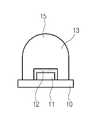
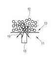
종래의 백색 LED는 청색 LED와 에폭시 및 실리콘과 같은 봉합수지에 분산된 파장 변환 물질로 사용되는 황색광을 방출하는 YAG:Ce 형광 분말을 조합하여 제조되며, 이는 미국 특허 5,998,925 및 6,069,440에 개시되어 있다. 이러한 파장 변환 물질은 청색 LED가 방출하는 광의 일부를 흡수하여 다른 파장에서 황색이나 황록색 광으로 재방출하기 위해 마련된다. 이러한 LED의 청색 광 및 형광체의 황록색 광이 조합되어 백색의 광이 인지된다. 도 1a 및 1b에는 일반적인 장치의 구조가 도시되어 있다. 도 1a에서, 부기판(10) 상에는 청색 LED(11)가 장착되어 있고, 이는 YAG:Ce 형광 분말(12)이 분산된 투명 매트릭스(13)로 덮여 있고, 보호 수지(15)에 의해 밀봉되어 있다. 도 1b에 도시된 바와 같이, 청색 LED(11)는 YAG:Ce 형광 분말(12)이 배치된 투명 매트릭스(13)로 둘러싸여 있다. 그러나, 이러한 시스템에서 사용되는 YAG:Ce 형광 분말의 입자크기는 대략 1-10㎛이기 때문에, 상기 투명 매트릭스(13) 내에 분산되어 있는 YAG:Ce 분말(12)은 강한 광 산란을 야기할 수 있다. 그 결과, 도 2에 도시된 바와 같이, 상기 청색 LED(11)로부터의 입사광(18) 및 YAG:Ce 분말로부터 나오는 황색 광(19) 모두 상당 부분 후방 산란되어 소멸되어 백색광 발광에 있어서 큰 손실을 일으킨다.Conventional white LEDs are fabricated by combining a blue LED and a YAG: Ce fluorescent powder that emits yellow light, which is used as a wavelength conversion material dispersed in a sealing resin such as epoxy and silicone, as disclosed in U.S. Patent Nos. 5,998,925 and 6,069,440 . Such a wavelength converting material is provided for absorbing a part of the light emitted by the blue LED and re-emitting it as yellow or yellow-green light at another wavelength. The blue light of the LED and the yellow green light of the phosphor are combined to recognize white light. 1A and 1B show the structure of a general device. 1A, a
이러한 문제를 해결하기 위한 방법 중 하나로, 파장 변환 물질로서 단일 세라믹 부재를 형성하는 방법이 있다. 이러한 세라믹 부재는 단일 혹은 복수의 형광체로 이루어진 복수의 세라믹층이나 투명층으로 구성될 수 있다. 이러한 투명 세라믹층은, 예를 들면 파장 변환 물질과 동일한 호스트 물질로 구성될 수 있으나 도핑물질은 전혀 포함하지 않을 수도 있다 (미국 특허 7,361,938). 이렇게 적층된 층은 또한 발광 세라믹 캐스트 테이프 형태일 수 있으며, 이들은 적층되어 함께 소성될 수 있다 (미국 특허 7,514,721 및 미국 공개공보 2009/0108507). 그러나, 이렇게 적층된 층은 일반적으로 고상 반응이나 공동 침전반응을 통해 제조된 내부 양자 효율 (IQE)이 낮은 가넷 분말로 형성되기 때문에, 본 발명자들은 이러한 발광층이 제조비용은 저렴하지만 발광성이 좋지 않다는 것을 인식하게 되었다. 액체 전구체를 고주파 열 플라즈마 처리하여 제조한 형광 나노입자는 높은 파장 변환 효율을 나타내고 (WO/2008/112710) 화학량론의 조절이 매우 용이하지만, 일반적으로 생산비용이 높다. 그 결과, 모두 플라즈마 나노입자로만 구성된 단일 세라믹판은 생산비를 증가시키게 될 것이다.As a method for solving such a problem, there is a method of forming a single ceramic member as a wavelength conversion material. Such a ceramic member may be composed of a plurality of ceramic layers or transparent layers made of a single phosphor or a plurality of phosphors. Such a transparent ceramic layer may, for example, consist of the same host material as the wavelength converting material, but may not contain any doping material (US Pat. No. 7,361,938). The laminated layer may also be in the form of a light-emitting ceramic cast tape, which may be laminated and fired together (U. S. Patent No. 7,514, 721 and U.S. Publication No. 2009/0108507). However, since the laminated layer is generally formed of a garnet powder having low internal quantum efficiency (IQE) produced through a solid-phase reaction or a coprecipitation reaction, the present inventors have found that such a luminescent layer is inexpensive to manufacture, It was recognized. Fluorescent nanoparticles prepared by high-frequency thermal plasma treatment of liquid precursors exhibit high wavelength conversion efficiency (WO / 2008/112710) and are easily controlled in stoichiometry, but generally have high production costs. As a result, a single ceramic plate consisting entirely of plasma nanoparticles will increase production costs.
또한, IQE가 높은 나노입자들이 세라믹으로 형성되는 경우, 반드시 높은 파장 변환 효율(wavelength conversion efficiency: WCE)을 지닌 세라믹 층으로 형성되는 것은 아니다. IQE는 발광물질에 부딪히는 광자가 발광물질에 의해 방출되는 광자로 변환되는 변환 효율 값이다. WCE는 청색광이 백색광으로 변하는 변환 효율 값을 말한다. 따라서, 백색광을 방출하는 장치에서, WCE는 특히 중요하다.In addition, when nanoparticles having high IQE are formed of ceramics, they are not necessarily formed of a ceramic layer having a high wavelength conversion efficiency (WCE). IQE is a conversion efficiency value at which a photon impinging on a luminescent material is converted into a photon emitted by the luminescent material. WCE is a conversion efficiency value at which blue light changes into white light. Thus, in devices emitting white light, WCE is particularly important.
본 발명자들은 두께가 수십 미크론/마이크로미터인 활성제 함량이 충분히 높은 형광 세라믹으로 이루어진 박막이 생산비를 현저하게 줄일 수 있다는 것을 인지하게 되었다. 그러나, 이러한 형광 박막은 색 변환에는 적합하지만, 약하고 취급이 어렵다. 따라서, 본 발명자들은 형광 분말의 발광 강도 감소 없이도 후방 산란으로 인한 손실을 최소화하면서 백색 LED의 광출력을 향상시킬 수 있는 효과적인 방법이 필요하다는 것을 인식하게 되었다.The present inventors have recognized that a thin film made of a fluorescent ceramic material having a sufficiently high activator content having a thickness of several tens of microns / micrometer can remarkably reduce the production cost. However, such a fluorescent thin film is suitable for color conversion, but is weak and difficult to handle. Therefore, the present inventors have recognized that there is a need for an effective method for improving the light output of a white LED while minimizing the loss due to back scattering without reducing the emission intensity of the fluorescent powder.
본 발명의 실시예에 따른 발광 세라믹 복합 적층체는 발광 물질을 포함하는 적어도 하나의 파장 변환 세라믹층 (발광층이라고도 함) 및 실질적으로 투명한 세라믹 물질로 이루어진 적어도 하나의 비발광층을 포함하며, 상기 파장 변환 세라믹층 및 상기 비발광층은 두께 방향으로 적층되어 있고, 상기 세라믹 복합 적층체의 파장 변환 효율 (WCE)은 목적하는 광 입사를 위해 적어도 약 0.650 (다른 실시예에 따르면 적어도 약 0.700)인 것을 특징으로 한다. 상기 비발광 투명층의 두께는 선택적으로 파장 변환 세라믹층의 두께보다 두껍다. 또한, 상기 파장 변환 세라믹층 및 비발광층은 선택적으로 소결 처리된 세라믹 테이프 캐스트층의 형상이다. 상기 발광층 자체의 파장 변환 효율 적어도 약 0.650이며, 선택적으로 (800nm 광에서 측정한) 투과율이 약 50% 내지 약 80%이다.A light emitting ceramic composite laminate according to an embodiment of the present invention includes at least one non-light emitting layer composed of at least one wavelength converting ceramic layer (also referred to as a light emitting layer) including a light emitting material and a substantially transparent ceramic material, Emitting layer is laminated in the thickness direction, and the wavelength conversion efficiency (WCE) of the ceramic composite laminate is at least about 0.650 (in other embodiments, at least about 0.700) for the desired light incidence do. The thickness of the non-emission transparent layer is optionally thicker than the thickness of the wavelength conversion ceramic layer. Further, the wavelength converting ceramic layer and the non-light emitting layer are in the form of a selectively sintered ceramic tape cast layer. The wavelength conversion efficiency of the light emitting layer itself is at least about 0.650, and the transmittance (measured at 800 nm light) is from about 50% to about 80%.
본 발명의 실시예에 따른 발광 세라믹 복합 적층체는 발광 물질 및 산란 물질을 포함하는 적어도 하나의 파장 변환 세라믹층 (발광층이라고도 함), 및 실질적으로 투명한 세라믹 물질로 이루어진 적어도 하나의 비발광층을 포함하며, 상기 파장 변환 세라믹층 및 비발광층은 두께 방향으로 적층되어 있고, 상기 세라믹 복합 적층체의 전투과율은 약 40% 내지 약 85%인 것을 특징으로 한다. 일 실시예에 따르면, 상기 발광 물질은 YAG:Ce이다. 일 실시예에 따르면, 상기 산란 물질은 산화 알루미늄을 포함한다.A light emitting ceramic composite laminate according to an embodiment of the present invention includes at least one wavelength converting ceramic layer (also referred to as a light emitting layer) including a light emitting material and a scattering material, and at least one non-light emitting layer made of a substantially transparent ceramic material The wavelength conversion ceramic layer and the non-emission layer are laminated in the thickness direction, and the total transmittance of the ceramic composite laminate is about 40% to about 85%. According to one embodiment, the luminescent material is YAG: Ce. According to one embodiment, the scattering material comprises aluminum oxide.
본 발명의 실시예에 따른 발광 장치는 (a) 경로를 갖는 광을 방출하기 위한 반도체 발광 소스 및 (b) 상기 반도체 발광 소스로부터 방출되는 광을 수신하기 위해 광의 경로 내에서 반도체 발광 소스에 인접하게 배치되어 있는 발광 세라믹 복합 적층체를 특징으로 하며, 상기 복합 적층체는 (b1) 발광 물질로 이루어지며 파장 변환 효율이 적어도 약 0.650인 파장 변환 세라믹층 및 (b2) 실질적으로 투명한 세라믹 비발광 물질로 이루어진 비발광층 포함한다. 일 실시예에 따르면, 상기 비발광 투명층은 선택적으로 상기 발광층보다 두께가 두꺼운 것을 특징으로 한다. 일 실시예에 따르면, 상기 파장 변환층 및 비발광층은 선택적으로 소결 처리된 세라믹 테이프 캐스트층의 형상이다.A light emitting device according to an embodiment of the present invention includes: (a) a semiconductor light emitting source for emitting light having a path and (b) a semiconductor light emitting source adjacent to a semiconductor light emitting source in the path of light for receiving light emitted from the semiconductor light emitting source (B1) a wavelength-converting ceramic layer having a wavelength conversion efficiency of at least about 0.650 and (b2) a substantially transparent ceramic non-luminescent material composed of a luminescent material, Emitting layer. According to one embodiment, the non-emission transparent layer is optionally thicker than the light emission layer. According to one embodiment, the wavelength conversion layer and the non-emission layer are in the form of a selectively sintered ceramic tape cast layer.
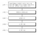
도 10에 도시된 바와 같이, 본 발명에 따른 발광 YAG:Ce 복합 적층체를 제조하는 방법은 (i) 비발광 물질로 이루어진 적어도 하나의 캐스트 테이프 및 파장 변환 효율이 적어도 약 0.650 이상인 발광 물질로 이루어진 적어도 하나의 캐스트 테이프를 마련하는 단계 (단계 1), (ii) 상기 캐스트 테이프의 일부를 적층하여 조립체를 형성하는 단계 (단계 2), (iii) 상기 조립체를 가압하여 프리폼(preform)을 제조하는 단계 (단계 3), (iv) 상기 프리폼을 가열하여 그린 프리폼을 제조하는 단계 (단계 4), 및 (v) 상기 그린 프리폼을 소결하여 발광 YAG:Ce 복합 적층체를 제조하는 단계 (단계 5)를 포함하는 것을 특징으로 한다.10, a method for fabricating a light emitting YAG: Ce composite laminate according to the present invention comprises the steps of: (i) providing at least one cast tape made of a non-luminescent material and a luminescent material having a wavelength conversion efficiency of at least about 0.650 or more (Ii) forming an assembly by laminating a part of the cast tape (step 2); (iii) pressing the assembly to produce a preform (Step 4) of preparing a green preform by heating the preform; and (v) sintering the green preform to produce a light emitting YAG: Ce composite laminate (step 5) And a control unit.
이상의 실시예 및 다른 실시예들은 하기에서 보다 상세히 설명하기로 한다.The above embodiments and other embodiments will be described in more detail below.
본 발명의 특징 및 이점을 요약하기 위해, 본 명세서에서는 본 발명의 특정한 목적 및 이점에 대해 기재한다. 물론 모든 목적 및 이점이 본 발명의 특정 실시예에 따라 구현될 수 있는 것은 아니다. 따라서, 예를 들면, 본 기술 분야의 통상의 기술자는 본 발명이 본 명세서에서 제시된 하나 또는 복수의 이점을 성취하고 최적화함으로써 여기서 제시된 그 밖의 목적이나 이점을 반드시 실현하지 않고도 구현되거나 실행될 수 있음을 인지해야 할 것이다.In order to summarize the features and advantages of the present invention, certain objects and advantages of the present invention are described herein. Of course, not all objects and advantages may be realized in accordance with any particular embodiment of the invention. Thus, for example, one of ordinary skill in the art will recognize that the present invention can be implemented or practiced without necessarily realizing other objects or advantages presented herein by accomplishing and optimizing one or more of the advantages set forth herein I will.
본 발명의 추가적인 측면, 특징 및 이점은 하기에 설명된 상세한 설명을 통해 분명해질 것이다.Further aspects, features and advantages of the present invention will become apparent from the following detailed description.
본 발명의 이러한 특징 및 그 밖의 특징은 바람직한 실시예를 도시한 도면을 참조하여 설명될 것이며, 이는 본 발명을 한정하기 위함이 아니라 예시하기 위함이다. 도면은 예시적인 목적을 위해 간단하게 도시되었다.
도 1a 및 1b는 종래의 백색 LED 장치의 단면도를 도시하며,
도 2는 종래의 백색 LED 장치 내에서 청색 LED에서 방출된 광이 미크론 크기의 황색 형광 분말에 의해 후방 산란되는 방법을 도시하며,
도 3은 본 발명의 일 실시예에 따른 파장 변환 세라믹 적층 구조의 단면도를 도시하며,
도 4는 본 발명의 다른 실시예에 따른 파장 변환 세라믹 적층 구조의 단면도를 도시하며,
도 5는 본 발명의 일 실시예에 따른 발광 장치의 단면도를 도시하며,
도 6은 본 발명의 일 실시예에 따른 발광 장치의 단면도를 도시하며,
도 7a은 본 발명의 일 실시예에 따른 발광 장치의 단면도를 도시하며,
도 7b는 본 발명의 일 실시예에 따른 발광 장치의 단면도를 도시하며,
도 7c는 본 발명의 일 실시예에 따른 발광 장치의 단면도를 도시하며,
도 8은 유동 기반 열화학적 합성(예를 들면 고주파 열 플라즈마)에 의한 YAG:Ce 분말, 고상 합성에 의한 분말 및 습식 용액(공동 침전)으로 합성한 분말의 내부 양자 효율(%)을 보여주는 그래프를 도시하며,
도 9는 유동 기반 열화학적 합성에 의한 YAG:Ce 분말로 형성되는 발광층, 고상 합성에 의한 분말로 형성되는 발광층 및 습식 용액(공동 침전)으로 합성한 분말로 형성되는 발광층의 파장 변환 효율 (mW/mW)과 투과율(%)의 관계를 보여주는 그래프를 도시하며,
도 10은 본 발명의 일 실시예 따른 발광층을 제조하는 방법을 도시하며,
도 11은 고상 합성에 의해 형성된 YAG:Ce로부터 제조된 세라믹 파장 변환판을 사용하는 발광 장치와 본 명세서에 개시된 실시예에 따라 제조한 두 구조의 파장 변환 효율(WCE)을 비교하는 그래프를 도시하며,
도 12는 본 명세서에 개시된 실시예에 따라 제조된 다른 예를 도시하며,
도 12a는 본 발명의 일 실시예에 따른 "실질적으로 반구형 구조"를 설명하며,
도 12b는 본 발명의 다른 실시예에 따른 "실질적으로 반구형 구조"를 도시하며,
도 12d는 본 발명의 다른 실시예에 따른 "실질적으로 반구형 구조"를 도시하며,
도 12d는 본 발명의 다른 실시예에 따른 "실질적으로 반구형 구조"를 도시하며,
도 12e는 본 발명의 일 실시예에 따른 "실질적으로 반구형 구조"의 높이와직경을 도시하며,
도 12f는 본 발명의 일 실시예에 따른 "실질적으로 반구형 구조"의 높이와직경을 도시하며,
도 13은 본 명세서에 개시된 실시예에 따라 제조된 다른 예를 도시하며
도 14는 본 명세서에 개시된 실시예를 제조하기 위한 과정 중 하나를 도시하며
도 15는 본 명세서에 개시된 다른 실시예를 제조하기 위한 과정 중 하나를 도시한다.These and other features of the present invention will now be described with reference to the drawings illustrating preferred embodiments, which are intended to be illustrative rather than limiting. The drawings are simplified for illustrative purposes.
1A and 1B show a cross-sectional view of a conventional white LED device,
Figure 2 shows how light emitted from a blue LED in a conventional white LED device is backscattered by a micron-sized yellow fluorescent powder,
3 shows a cross-sectional view of a wavelength conversion ceramic laminate structure according to an embodiment of the present invention,
Figure 4 shows a cross-sectional view of a wavelength-shifting ceramic laminate structure according to another embodiment of the present invention,
5 is a cross-sectional view of a light emitting device according to an embodiment of the present invention,
6 is a cross-sectional view of a light emitting device according to an embodiment of the present invention,
7A is a cross-sectional view of a light emitting device according to an embodiment of the present invention,
7B is a cross-sectional view of a light emitting device according to an embodiment of the present invention,
7C shows a cross-sectional view of a light emitting device according to an embodiment of the present invention,
8 is a graph showing the internal quantum efficiency (%) of powders synthesized by YAG: Ce powder, solid phase synthesis and wet solution (co-precipitation) by flow-based thermochemical synthesis (e.g., high frequency thermal plasma) Respectively,
9 is a graph showing the wavelength conversion efficiency (mW / cm 2) of a light emitting layer formed of a powder synthesized from a light emitting layer formed of a YAG: Ce powder by a flow-based thermochemical synthesis, a light emitting layer formed of powder by solid phase synthesis, mW) and transmittance (%), and FIG.
10 illustrates a method of manufacturing a light emitting layer according to an embodiment of the present invention,
11 shows a graph comparing a wavelength conversion efficiency (WCE) of a light emitting device using a ceramic waveguide plate made of YAG: Ce formed by solid phase synthesis and two structures manufactured according to the embodiment disclosed herein ,
Figure 12 shows another example made in accordance with the embodiments disclosed herein,
12A illustrates a " substantially hemispherical structure "according to one embodiment of the present invention,
Figure 12B shows "a substantially hemispherical structure" according to another embodiment of the present invention,
12D shows a " substantially hemispherical structure "according to another embodiment of the present invention,
12D shows a " substantially hemispherical structure "according to another embodiment of the present invention,
Figure 12E illustrates the height and diameter of a "substantially hemispherical structure" according to one embodiment of the present invention,
Figure 12f illustrates the height and diameter of a "substantially hemispherical structure" according to an embodiment of the present invention,
Figure 13 shows another example made according to the embodiments disclosed herein
Figure 14 shows one of the processes for manufacturing the embodiments disclosed herein
FIG. 15 illustrates one of the processes for manufacturing another embodiment disclosed herein.
형광체용 발광물질을 제조하는데 있어서 다양한 방법이 이용될 수 있는데, 여기에는 습식 화학 공동침전, 열수 합성, 초임계 합성, 고상 반응, 연소법, 레이저 열분해, 화염 스프레이, 스프레이 열분해 및 플라즈마 합성법이 포함된다. 이 중에서도, 특히 레이저 열분해, 화염 스프레이, 스프레이 열분해 및 플라즈마 합성법과 같은 유동 기반 열화학적 합성 방법이 고순도, 결정 불량 방지 및 효율이 높은 형광체형성의 측면에서 적절하다. 이러한 방법 중, 플라즈마 합성법, 특히 무선 주파수 유도 결합 열 플라스마 합성법은 가연성 가스(화염 스프레이 내의 메탄과 같은 연료)를 사용하지 않고, 합성 중 생성물이 전극과 전혀 접촉하지 않기 때문에 최종 생산물의 순도가 매우 높아진다. 공개특허 WO2008/112710에 개시된 바와 같이, 원자화 형태의 전구체 용액을 고주파 열 플라즈마 화염에 통과시켜 형광입자로 응집하도록 함으로써 크기 조절가능하고, 높은 순도 및 높은 발광 효율을 특징으로 하는 형광입자를 제조할 수 있다. 이러한 입자는 적절한 필터를 사용하여 수거될 수 있다. 예를 들면, 화학양론적으로 질산 이트륨, 질산 알루미늄 및 질산 세륨을 포함하는 수용액을 사용하여 이 용액을 고주파 플라즈마 화염의 중심에서 이액 원자화를 통해 원자화하여, 전구체를 증발 및 분해시킨 후 Y-Al-O 입자를 응집함으로써 세륨이 도핑된 산환 이트륨 알루미늄 입자를 합성할 수 있다. 이러한 입자는 적절한 여과 방법을 통해 폐기가스로부터 추출할 수 있다. 이렇게 수거된 입자는 1000도 이상의 온도의 적절한 용광로에서 열 어닐링하면 완벽하게 또는 거의 완벽하게 순수한 세륨이 도핑된 이트륨 알루미늄 가넷 입자 상태로 변화되며, 이러한 가넷 입자의 파장변환 효율은 세라믹 층이나 시트 형태에서 적어도 0.65의 값을 갖는다. 도핑물질의 값은 바람직한 목적에 따라 결정되며, 본 기술 분야의 통상의 기술자는 본 발명의 기본적인 의도를 벗어나지 않는 범위 내에서 도핑물질 값을 변형할 수 있다. 본 발명의 발명자는 도 8 및 9에 도시된 바와 같이, 형광체를 합성하는 다른 방법에 의해 얻어진 물질을 포함하는 세라믹과 비교했을 때 고주파 플라즈마 합성 형광체를 포함하는 세라믹층이 최고의 파장변환 효율을 갖는다는 것을 발견하게 되었고, 이러한 사실은 하기의 실시예를 참조하여 설명한다.Various methods can be used in the production of the luminescent material for the phosphor, including wet chemical co-precipitation, hydrothermal synthesis, supercritical synthesis, solid phase reaction, combustion method, laser pyrolysis, flame spraying, spray pyrolysis and plasma synthesis. Particularly, a flow-based thermochemical synthesis method such as laser pyrolysis, flame spraying, spray pyrolysis and plasma synthesis is suitable in terms of high purity, prevention of crystal defect, and formation of phosphor with high efficiency. Among these methods, the plasma synthesis method, particularly the radio frequency inductively coupled thermal plasma synthesis method, does not use a combustible gas (fuel such as methane in a flame spray), and the product in the synthesis does not contact the electrode at all, . Fluorescent particles can be prepared which are size-adjustable and characterized by high purity and high luminous efficiency by allowing the precursor solution in atomized form to pass through a high-frequency thermal plasma flame to aggregate into fluorescent particles, as disclosed in published patent application WO2008 / 112710 have. These particles can be collected using an appropriate filter. For example, the solution may be atomically atomized at the center of a high-frequency plasma flame using an aqueous solution comprising yttrium nitrate, aluminum nitrate and cerium nitrate, stoichiometrically, evaporating and decomposing the precursor, O particles can be agglomerated to synthesize oxalated yttrium aluminum particles doped with cerium. These particles can be extracted from the waste gas by suitable filtration methods. The particles thus collected are thermally annealed in an appropriate furnace at a temperature of 1000 ° C or higher and are transformed into completely or almost completely pure cerium-doped yttrium aluminum garnet particles. The wavelength conversion efficiency of such garnet particles is in the form of a ceramic layer or sheet At least 0.65. The value of the doping material is determined according to the desired purpose, and a person skilled in the art can modify the value of the doping material within the scope of the basic intention of the present invention. As shown in FIGS. 8 and 9, the inventors of the present invention have found that a ceramic layer including a high-frequency plasma-synthesized phosphor has the highest wavelength conversion efficiency as compared with a ceramic including a material obtained by another method of synthesizing a phosphor And this fact will be explained with reference to the following embodiments.
본 명세서에서는 조건 및/또는 구조를 구체적으로 명시하지 않으며, 본 기술 분야의 통상의 기술자는 본 명세서를 고려하여 정기적인 실험을 통해 이러한 조건 및/또는 구조 및 필요에 따라 본 명세서에 참고로 모두 포함되는 WO2008/112710에 개시된 고주파 열 플라즈마 합성에 의한 세륨이 도핑된 YAG 분말을 제조하는 방법을 용이하게 제공할 수 있다. 예를 들면, 세륨이 도핑된 YAG 분말로 이루어진 세라믹층을 얻기 위해, 파장 변환 효율이 적어도 0.65인 세라믹 복합 적층체를 제공하는 경우, 세라믹 내의 도핑물질이나 활성제의 분산을 조절 변수로 이용할 수 있다. 분산 정도가 증가하면, 상기 적층체의 파장 변환 효율은 0.65이상으로, 세라믹 적층체는 파장 변환 효율이 0.65보다 작은 것에 비해 대단히 향상된다. 본 기술 분야에서는 WCE값의 중요성이 인식되지 않고 있으며, WCE값을 조절할 수 없고, WCE값이 적어도 0.65인 세라믹 적층체를 지속적으로 생산할 수 없다.In this specification, conditions and / or structures are not specifically described, and a person skilled in the art will, in view of this specification, include all of these conditions and / or structures, and if necessary, A method for producing cerium-doped YAG powder by the high-frequency thermal plasma synthesis disclosed in WO2008 / 112710 can be easily provided. For example, in the case of providing a ceramic composite laminate having a wavelength conversion efficiency of at least 0.65 in order to obtain a ceramic layer composed of cerium-doped YAG powder, the dispersion of the doping material or the activator in the ceramic can be used as a control parameter. When the degree of dispersion is increased, the wavelength conversion efficiency of the laminate is 0.65 or more, and the ceramic laminate is greatly improved as compared with the case where the wavelength conversion efficiency is less than 0.65. The importance of the WCE value is not recognized in the art, the WCE value can not be controlled, and the ceramic laminate having a WCE value of at least 0.65 can not be continuously produced.
도 3에 도시된 바와 같이, 본 발명의 일 실시예에서는 파장 변환 효율이 적어도 약 0.650이며 발광물질을 포함하는 적어도 하나의 파장 변환 세라믹 층(22)과 실질적으로 투명한 물질로 이루어진 적어도 하나의 비발광 층(24) (본 실시예에서는 세 개의 층(24a, 24b 및 24c))을 포함하는 복합 적층체(20)를 제공하며, 상기 비발광 층(24)의 두께는 선택적으로 상기 파장변환층(22)의 두께보다 두꺼울 수 있다. 상기 파장변환층 및 비발광층은 선택적으로 소결된 세라믹 테이프 캐스트층의 형태가 될 수 있다. 일 실시예에 따르면, 각각의 비발광층(24)은 YAG분말 뿐 아니라 산화 알루미늄(Al2O3) 분말, 산화 이트륨(Y2O3) 분말 및 그 밖의 산화물 분말로 형성될 수 있으며, 고체상 반응(solid state reaction: SSR) 합성과 같은 저렴한 방법으로 제조할 수 있다. 일 실시예에서는 비발광층은 다른 성분으로 도핑되지 않거나 비발광 특징을 나타낼 수 있을 정도로만 도핑될 수 있다. 일 실시예에서는 각각의 파장변환 세라믹층(22)은 세륨이 도핑된 YAG분말로 이루어지는 것이 바람직하며, 이는 발광층에 효과적으로 높은 파장 변환 효율(예를 들면, 0.70, 0.75와 같이 0.65 이상)을 부여하기 위해 고주파 열 플라즈마 합성에 의해 제조될 수 있다. 다른 실시예에 따르면, 각각의 파장변환 세라믹층(22)과 각각의 비발광층(24)은 소결 처리된 세라믹 테이프 캐스트층의 형태이다. 일 실시예에 따르면, 상기 발광 물질은 유동 기반 열화학적 합성에 의해 형성된 물질이다. 다른 실시예에 따르면, 상기 발광물질은 고주파 유도결합 열 플라즈마 합성으로 형성된 세륨(Cerium) 도핑 이트륨 알루미늄 가닛(Yttrium aluminum garnet, 이하 YAG:Ce로 표시함)을 포함한다.3, in an embodiment of the present invention, at least one wavelength
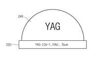
일 실시예에 따르면, 상기 파장변환 세라믹층(22)의 두께는 약 10 내지 약1000μm 이다. 다른 실시예에 따르면, 상기 파장변환 세라믹층(22)의 두께는 약 15 내지 100μm 이다. 또 다른 실시예에 따르면, 상기 파장변환 세라믹층(22)의 두께는 약 20 내지 80μm 이다. 또 다른 실시예에 따르면, 상기 파장변환 세라믹층(22)의 두께는 약 30 내지 70μm 이다. 또 다른 실시예에 따르면, 상기 파장변환 세라믹층(22)의 두께는 상기에서 언급한 수치 중 어느 두 개의 값 사이에 있는 값일 수 있다. 일 실시예에서는, 상기 파장변환 세라믹층(22)은 파장변환 세라믹층을 이루는 주요 성분에 대해 농도가 약 0.5 내지 약 10.0몰%인 활성 도핑물질을 포함하며, 상기 실질적으로 투명한 세라믹 물질은 도핑되지 않은 가넷 물질이다. 일 실시예에 따르면, (이트늄 함량에 대한) 상기 도핑물질의 농도(몰%)는 약 35μm 두께 YAG:Ce층에 대해 약 1.75%이다. 일 실시예에 따르면, 상기 도핑물질의 농도는 약 65 내지 약 325μm 두께 YAG:Ce층에 대해 약 1.75%이다. 상기 파장변환 세라믹층(22)은 단일층이거나 각 층이 상기에서 언급된 두께를 갖는 복수의 층일 수 있다. 일 실시예에 따르면, 상기 도핑물질의 농도(1.75%)는 5% 내지 50%만큼, 예를 들면 바람직한 발광 특성을 나타낼 수 있는 정도의 범위 내에서 변경할 수 있다. 일 실시예에 따르면, 상기 도핑물질의 농도는 약 35 내지 약 40μm 두께의 YAG:Ce층에 대해 약 1.75 내지 2.0%이며, 상기 비발광층은 약 350 내지 약 600μm이다.According to one embodiment, the thickness of the wavelength converting
일 실시예에 따르면, 상기 비발광층(24)은 약 30 내지 약 1000μm이다. 다른 실시예에 따르면, 상기 비발광층의 두께는 약 50 내지 750μm이다. 또 다른 실시예에 따르면, 상기 비발광층의 두께는 약 300 내지 500μm이다. 또 다른 실시예에 따르면, 상기 비발광층의 두께는 상기에서 언급한 수치 중 어느 두 개의 값 사이에 있는 값일 수 있다. 상기 비발광층(24)은 단일층이거나 각 층이 상기에서 언급된 바와 같은 두께를 갖는 복수의 층으로 이루어질 수 있다. 일 실시예에 따르면, 도 3에 도시된 각 층 24a, 24b 및 24c의 두께를 합한 총 두께는 상기에서 언급한 범위의 두께일 수 있다. 다른 실시예에서 상기 비발광층의 총 두께는 상기 (복수의) 파장변환 세라믹층의 총 두께보다 클 수 있다. 일 실시예에 따르면, 각각의 비발광층 두께는 각각의 파장변환 세라믹층 두께보다 클 수 있다. 다른 실시예에 따르면, 각각의 비발광층은 두께가 약 50μm 내지 약 200μm, 약 60μm 내지 175μm, 85μm 내지 155μm, 또는 상기에서 언급된 수치 중 어느 두 개의 값 사이의 두께를 갖는 (도핑되지 않은 호스트 물질을 포함하는) 캐스트 테이프 형태이다. 일 실시예에 따르면, 상기 비발광층(24)에 대한 상기 파장변환 세라믹층(22)의 두께 비율은 선택적으로 대략 1/1 이하 내지 대략 1/250 이하이다. 다른 실시예에 따르면, 상기 비발광층(24)에 대한 상기 파장변환 세라믹층(22)의 두께 비율은 대략 1/5 이하 내지 대략 1/20 이하이다. 또 다른 실시예에 따르면, 상기 비발광층(24)에 대한 상기 파장변환 세라믹층(22)의 두께 비율은 대략 35/420이며, 다른 실시예에서는 약 40/450이다. 또한, 일 실시예에 따르면, 상기 비발광층(24)에 대한 상기 파장변환 세라믹층(22)의 두께 비율은 약 1/3 이하이다. 다른 실시예에 따르면, 상기 비발광층(24)에 대한 상기 파장변환 세라믹층(22)의 두께 비율은 약 1/10 이하이다. 다른 실시예에 따르면, 상기 비발광층(24)에 대한 상기 파장변환 세라믹층(22)의 두께 비율은 상기에서 언급된 수치 중 어느 두 개의 값 사이의 값일 수 있다.According to one embodiment, the
일 실시예에 따르면, 선택된 물질로 이루어진 파장변환 세라믹층(22)은 높은 파장변환 효율을 나타낸다. 상기 파장변환 효율은 상기 물질이 하나 이상의 파장에서 방사선을 흡수하여 하나 이상의 다른 파장에서 다시 방출하는 효율로 정의할 수 있다. 상기 파장변환 효율은 하기에 설명되는 바와 같이 산출할 수 있다.According to one embodiment, the wavelength
도 7b에 도시된 바와 같이, 본 발명의 일 실시예에 따르면, 발광 물질 및 산란 물질을 포함하는 적어도 하나의 파장변환 세라믹층(22a) 및 실질적으로 투명한 물질로 이루어진 적어도 하나의 비발광층(24, 여기서는 세 개 (24a, 24b, 24c))을 포함하는 발광 세라믹 복합 적층체(20)가 제공된다. 여기서 사용되는 용어 "산란 물질"은 상기 발광 물질과 다른 굴절률을 갖고 실질적으로 투명한 물질을 의미한다. 일 실시예에 따르면, 상기 산란 물질은 발광 물질 전반에 걸쳐 분산되어 있는 서로 분리되어 있는 복수의 산란 센터 내에 배치되어 있다. 일 실시예에 따르면, 상기 산란 물질은 이에 제한되지는 않으나 Al2O3, Y2O3, CaO, TiO2, MgO, La2O3, CeO2, Nd2O3, Tb4O7, Eu2O3, BaO, Gd2O3, 등을 포함한다. 일 실시예에 따르면, 상기 발광 물질은 적어도 하나의 형광 물질을 포함하며, 상기 산란 물질은 상기 형광 발광 물질에 대응하는 적어도 하나의 금속 산화물을 포함한다. 일 실시예에 따르면, 상기 발광 물질은 희토류로 도핑된 Y3Al5O12 (예를 들면, Y3Al5O12:Ce)를 포함하며, 상기 산란 물질은 Y3Al5O12:Ce에 대응하는 적어도 하나의 금속 산화물, 예를 들면, Y2O3, Al2O3, YAlO3 (Yttrium Aluminum Perovskite or YAP)와 Y4Al12O9 (Yttrium Aluminum Monoclinic or YAM) 중 적어도 하나를 포함한다.7B, according to an embodiment of the present invention, at least one wavelength
일 실시예에 따르면, 상기 발광 물질의 부피는 파장변환 세라믹층의 총 부피의 약 85% 내지 99.99%이다. 일 실시예에 따르면, 상기 산란 물질의 부피는 파장변환 세라믹층 내의 발광 물질 및 산란 물질을 합한 총 부피의 약 15% 내지 약 0.01%이다. 일 실시예에 따르면, 상기 발광 물질의 부피비 (volume%)는 약 90% 내지 약 99.99%, 약 95% 내지 약 99%, 또는 약 98% 내지 약 99%이며, 상기 산란 물질의 부피비는 약 10% 내지 약 0.01%, 약 7% 내지 약 0.01%, 약 5% 내지 약 0.01%, 약 3% 내지 약 0.01%, 약 2% 내지 약 0.01%, 또는 약 1% 내지 약 0.01%이다.According to one embodiment, the volume of the luminescent material is about 85% to 99.99% of the total volume of the wavelength converting ceramic layer. According to one embodiment, the volume of the scattering material is from about 15% to about 0.01% of the total volume of luminescent material and scattering material in the wavelength converting ceramic layer. According to one embodiment, the volume percentage of the luminescent material is about 90% to about 99.99%, about 95% to about 99%, or about 98% to about 99%, and the volume ratio of the scattering material is about 10 % To about 0.01%, about 7% to about 0.01%, about 5% to about 0.01%, about 3% to about 0.01%, about 2% to about 0.01%, or about 1% to about 0.01%.
일 실시예에 따르면, 상기 발광 물질 및 산란 물질을 포함하는 복합 적층체는 산란 물질에 대한 발광 물질의 비가 발광 물질 내에서 매우 우세한 경우, 예를 들면, 발광 물질이 약 85%이고 산란 물질이 약 15%인 경우이거나, 발광 물질이 약 90%이고 산란 물질이 약 10%인 경우이거나, 발광 물질이 약 95%이고 산란 물질이 약 5%인 경우이거나, 발광 물질이 약 98%이고 산란 물질이 약 2%인 경우 및 발광 물질이 약 99%이고 산란 물질이 약 1%인 경우에, 높은 투명성 및 제한적인 후방산란의 균형을 조절하는데 있어 특히 효과적이다.According to one embodiment, when the ratio of the light emitting material to the scattering material is very high in the light emitting material, for example, when the light emitting material is about 85% and the scattering material is about 15%, or about 90% of the luminescent material and about 10% of the scattering material, or about 95% of the luminescent material and about 5% of the scattering material, or about 98% Especially about 2%, and when the luminescent material is about 99% and the scattering material is about 1%, it is particularly effective in controlling the balance of high transparency and limited backscattering.
일 실시예에 따르면, 상기 파장변환 세라믹층은 부피비로 약 85% 내지 약 99.99%의 발광 물질 및 약 15% 내지 약 0.01%의 산란 물질을 포함한다. 상기 적어도 하나의 소결 세라믹 적층체는 상기 발광 성분으로부터 방출되는 빛의 적어도 일부를 흡수하여 제2 피크 파장의 빛을 방출할 수 있으며, 상기 소결 세라믹 적층체는 제2 피크 파장에서의 총 광투과율이 약 40%를 초과한다.According to one embodiment, the wavelength converting ceramic layer comprises from about 85% to about 99.99% luminescent material and from about 15% to about 0.01% scattering material by volume. The at least one sintered ceramic laminate may absorb at least a part of light emitted from the light emitting component and emit light of a second peak wavelength. The sintered ceramic laminate may have a total light transmittance at a second peak wavelength ≪ / RTI > exceeds about 40%.
일 실시예에 따르면, 상기 복합 적층체는 산란 물질에 대한 발광 물질의 부피비가 산란 물질 내에서 매우 우세한데, 예를 들면, 산란 물질이 약 85%이고 발광 물질이 약 15%, 산란 물질이 약 90%이고 발광 물질이 약 10%, 산란 물질이 약 95%이고 발광 물질이 약 5%, 산란 물질이 약 98%이고 발광 물질이 약 2%인 경우 및 산란 물질이 약 99%이고 발광 물질이 약 1%일 수 있다.According to one embodiment, the composite laminate is characterized in that the volume ratio of the luminescent material to the luminescent material is very predominant in the luminescent material, for example, about 85% of the luminescent material, about 15% of the luminescent material, 90%, the luminescent material is about 10%, the scattering material is about 95%, the luminescent material is about 5%, the scattering material is about 98%, the luminescent material is about 2% About 1%.
일 실시예에 따르면, 상기 파장변환 세라믹 층 내에서의 산란 물질에 대한 발광 물질의 부피비는 약 85% 내지 약 99.99%의 산란 물질 및 약 15% 내지 약 0.01%의 발광 물질로 이루어진다. 상기 적어도 하나의 소결 세라믹 판은 상기 발광 성분으로부터 방출되는 빛의 적어도 일부를 흡수하여 제2 피크 파장의 빛을 방출할 수 있으며, 상기 소결 세라믹 적층체는 제2 피크 파장에서의 총 광투과율이 약 40%를 초과한다.According to one embodiment, the volume ratio of the luminescent material to the scattering material in the wavelength converting ceramic layer is about 85% to about 99.99% of the scattering material and about 15% to about 0.01% of the luminescent material. The at least one sintered ceramic laminate may absorb at least a part of light emitted from the light emitting component and emit light of a second peak wavelength. The sintered ceramic laminate may have a total light transmittance at a second peak wavelength of about ≪ / RTI >
이론적으로 한정되는 것은 아니지만, 본 발명자들은 파장 변환 세라믹층 내에 산란 물질 및/또는 산란 센터를 포함시킴으로써, 산란 물질에 입사하며 발광상 물질 및 예를 들면, 대기와 같은 주변 환경 사이의 중간 정도의 동일한 굴절률을 갖는 광이 파장 변환 세라믹층 및/또는 비발광층 및 주변 환경 사이의 광학적 간섭에 의해 덜 지연되도록 할 수 있다고 판단하였다. 일단 발광 물질에 의해 방출된 광은 산란 물질로 입사하고, 이는 굴절률 및 굴절각으로 인한 파장 변환 세라믹층 및 공기 사이의 굴절률 차에 의해 보다 덜 지연되어 방출된 광을 더 추출할 수 있다고 생각한 것이다.By including the scattering material and / or the scattering center in the wavelength converting ceramic layer, theoretically, the present inventors have found that by introducing scattering material and / or scattering center into the scattering material, It was determined that the light having the refractive index could be less delayed by the optical interference between the wavelength converting ceramic layer and / or the non-light emitting layer and the surrounding environment. Once the light emitted by the luminescent material is incident as a scattering material, it is thought that it is possible to further extract the emitted light due to the retardation due to the refractive index difference between the wavelength converting ceramic layer and the air due to the refractive index and refraction angle.
일 실시예에 따르면, 도 7c에 도시된 바와 같이 상기 복합 적층체(20)는 상기 적어도 하나의 비발광층(24j)에 대향하는 상기 적어도 하나의 파장변환 세라믹층에 적층된 적어도 하나의 추가적인 비발광층(24i)을 더 포함한다. 일 실시예에 따르면, 상기 비발광층은 상기 발광층보다는 작지만 공기 공극이나 주변 환경보다는 큰 굴절률을 갖는 물질을 포함한다. 일 실시예에 따르면, 상기 비발광층은 굴절률이 약 1.63인 산화 알루미늄(Al2O3)을 포함한다. 이론적으로 제한되지는 않지만, 본 실시예에서는 굴절률의 차이가 상기 발광층 내에서 방출된 광을 안내하여, 산란 물질로 향하는 광을 증가시킴으로써, 상기에서 언급한 바와 같이 광 추출을 향상시킨다고 생각하였다. 다른 실시예에 따르면, 상기 비발광층은 도핑물질 차단 성분을 포함하며, 이러한 도핑물질 차단 성분은 상기 발광층으로부터 비발광층으로 산란되는 세륨과 같은 도핑물질의 양을 실질적으로 감소시킨다. 일 실시예에 따르면, 상기 도핑물질 차단 물질 및 비발광물질은 동일한 것일 수 있다. 일 실시예에 따르면, 도핑물질 차단 물질 및 비발광 물질로 사용될 수 있는 물질은 산화 알루미늄(Al2O3)을 포함한다.According to one embodiment, as shown in FIG. 7C, the
실시예를 통해 하기에서 설명되는 도 9를 참조하면, 플라즈마에 의해 생성된 YAG:Ce와 같은 유동 기반 열화학적 합성 물질로부터 제조된 발광층을 포함하는 세라믹 적층 복합체의 파장 변환 효율은 적어도 0.600, 바람직하게는 0.650 이상이며, 일 실시예에서는 적어도 0.675, 다른 실시예에서는 적어도 0.700 값을 갖는다. 이론적으로 제한되지는 않지만, 본 발명자들은 적어도 원자 수준의 전구체 분산의 불균질성을 제어 및/또는 상기 파장 변환 세라믹층(22) 내의 세륨의 분산을 증가시킴으로써 플라즈마에 의해 생성된 YGA:Ce을 포함하는 세라믹 적층 복합체의 파장 변환 효율은 항상 0.650 이상으로 유지할 수 있다 (도 9를 참고하면, 플라즈마에 의해 생성된 YGA:Ce 중 일부의 파장 변환 효율은 0.650 미만이며, 이는 전구체, 특히 세륨과 같은 도핑물질이나 활성 성분이 발광 물질 전반에 걸쳐 충분히 균일하게 분산되어 있지 않기 때문이다). 이와 반대로, 고체상 반응으로 합성된 YAG:Ce로 이루어진 발광층의 파장 변환 효율은 약 0.625 이하이다. 또한, 공동 침전에 의해 합성된 형광체로 이루어진 발광층의 파장 변환 효율은 0.200 이하이다.9, described below, the wavelength conversion efficiency of a ceramic laminated composite comprising a light emitting layer made from a flow-based thermochemical synthesis material such as YAG: Ce produced by plasma is at least 0.600, preferably Is at least 0.650, in one embodiment at least 0.675, in other embodiments at least 0.700. Although not intending to be bound by theory, the inventors have found that by controlling the inhomogeneity of at least atomic level precursor dispersion and / or increasing the dispersion of cerium in the wavelength converting
일 실시예에 따르면, 도 3에 도시된 바와 같이, 상기 파장 변환 세라믹층(22)은 비발광층(24) 하부에 배치된다. "하부"라는 표현은 비발광층 및 발광장치 에 대한 발광층의 상대적인 위치를 의미하는 것으로, 예를 들어 상기 발광층이 비발광층 "하부"에 있다는 것은 상기 발광층이 비발광층에 비해 광원에 가깝게 위치한다는 것을 의미하며 (상기 발광층은 비발광층과 광원 사이에 위치한다), "상부"라는 표현은 비발광층에 비해 광원에 먼쪽에 위치한다는 것을 의미한다 (상기 비발광층은 발광층과 광원 사이에 위치한다). 이러한 상대적인 위치는 발광특성적인 면에서 두 개의 층이 물리적으로 서로 접하고 있는 경우 및 두 개의 층이 기능적으로 서로 접하고 있는 경우를 포함한다.According to one embodiment, as shown in FIG. 3, the wavelength converting
일 실시예에 따르면, 도 4에 도시된 바와 같이, 상기 파장 변환 세라믹층(22)은 적어도 두 개의 비발광층(24d, 24e) 사이에 개재된다. 일 실시예에 따르면, 상기 적층 복합체 적어도 하나의 파장 변환 세라믹층(22) 위에 적층된 적어도 하나의 추가 비발광층(24e)을 더 제공하며, 이는 상기 적어도 하나의 제1 비발광층(24d)의 반대 방향에 위치한다.According to one embodiment, as shown in Fig. 4, the wavelength converting
도 5에 도시된 바와 같이, 일 실시예에 따르면, 상기 파장 변환 세라믹층(22)은 비발광층(24) 및 광원 (26, 예를 들면, 발광 반도체) 인접에 배치된다. 일 실시예에 따르면, 상기 적층 복합체(20)은 광원(26)으로부터 방출되는 광(28)의 경로 상에 위치한다. 일 실시예에 따르면, 상기 광원(26)은 n형 영역 및 p형 영역 사이에 위치한 발광층을 포함하는 반도체 발광장치이다. 다른 실시예에 따르면, 상기 광원(26)은 애노드, 캐소드 및 그 사이에 위치하는 유기 발광층 또는 발광층을 포함하는 유기 발광장치이다. 다른 실시예에 따르면, 상기 발광 변환 세라믹층(22)은 비발광층(24) 상부에 위치한다. 즉, 상기 비발광층(24)은 도 6에 도시된 바와 같이 파장 변환 세라믹층(22)과 광원(26)이 방출하는 광(28)의 경로 사이에 위치한다. 다른 실시예에 따르면, 상기 비발광층(24f)은 파장 변환 세라믹층(22) 및 광원(26) 사이에 위치한다. 다른 실시예에 따르면, 도 7a에 도시된 바와 같이, 상기 파장 변환 세라믹층(22)은 비발광층(24f, 24g) 사이에 위치하며 (상기 광원(26)에 대해 각각의 비발광층(24g, 24f)에 가깝게 및 멀게 위치하며) 광원(26)에서 방출하는 광(28)의 경로 상에 위치한다. 일례에서 상기 발광층은 용광로 물질로부터 발생하는 오염물질을 포함하는 소결 환경에 매우 취약할 수 있다. 예를 들면, 이론적으로 제한되지는 않지만, 오염을 일으킬 수 있는 물질이 층 표면에 퇴적될 수 있고, 역조반응이 일어나 이에 따라 부분적으로는 불순물에 취약한 YAG 결정체 내의 세륨과 같은 희토류 도핑 물질로 인해 발광 효율이 떨어질 수 있다. 발광층을 보호하기 위해서, 비발광층/발광층/발광층으로 이루어지는 개재 구조가 적절하게 선택될 수 있으며, 이에 따라 원치 않는 효율 감소를 방지할 수 있다. 다른 실시예에 따르면, 상기 발광층은 두 개 이상의 비발광 투명층 사이에 개재됨으로써 수분이나 열과 같은 동작 시의 위험요소로부터 보호될 수 있다. 비발광층(240)이 파장 변환 세라믹층(220) 상부에 위치한 경우, 상기 비발광층(240)은 실질적으로 반구형의 볼록 세라믹 부재를 포함하며, 이러한 예가 도 12에 도시되어 있다. 본 기술 분야의 통상의 기술자는 본 발명에서 예시한 실시예를 산란 센터를 포함하는 발광층을 포함하는 적층 복합체를 제공하는데 있어서도 적용할 수 있다.As shown in FIG. 5, according to one embodiment, the wavelength converting
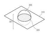
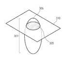
도 12를 다시 참조하면, 일 실시예에서 비발광층(240)은 "실질적으로 반구형상"인데, 이는 비발광층(240)의 표면이 도 12a 내지 12c에 도시된 바와 같이 회전타원체(301)가 평면(310)에 의해 절단될 때 얻어지는 작은 형상(305)에 의해 형성된 것을 의미한다. 상기 회전타원체는 도 12a에 도시된 바와 같은 구체일 수 있고, 도 12b에 도시된 바와 같은 장축 타원체이거나, 도 12c에 도시된 바와 같은 회전 타원체 등일 수 있다. 또는, 도 12d에 도시된 바와 같이 "커버"라고도 하는 상기 비발광층은 원통(315)의 상부에 작은 형상(305)을 갖는 원통(315)을 포함하는 경우 "실질적으로 반구형상"이다. 이러한 비발광층은 일반적인 형태 이외에도 다양한 형상으로 이루어질 수 있다. 예를 들면, 당해 기술 분야에서 일반적인 형태라고 인식되는 범위 내에서 일반적인 실질적으로 반구형상이 표면 거칠기, 편평도 또는 질감을 변경할 수 있고, 개구부나 함몰부를 배열하는 것과 같이 부차적인 구조를 표면에 추가 할 수 있다. 일 실시예에 따르면, 상기 실질적으로 반구형상인 커버는 원형 기저를 포함하며, 이는 도 12e를 참조하면, 상기 타원체(301)를 사용하여 평면에 교차함으로써 형성된 형상(320)을 의미한다.12, in one embodiment, the
일 실시예에 따르면, 도 12e에 도시된 바와 같이 "높이"라는 용어는 상기 타원체를 절단하는 평면으로부터 작은 형상(305)의 상부까지의 거리(340)를 의미한다. 일 실시예에 따르면, "직경"이라는 용어는 형상(320)을 가로지르는 가장 긴 거리를 의미한다. 일 실시예에 따르면, "높이"이란 용어는 거리(345)를 의미하며, 이는 원통(325)의 기저의 평면으로부터 작은 형상(305)의 상부까지의 거리를 말한다. 일 실시예에 따르면, "직경"이란 용어는 원통(523)의 기저의 직경(337)을 의미한다. 일 실시예에 따르면, 상기 실질적으로 구형상의 커버의 높이/직경 비율은 약 0.2 내지 약 2, 약 0.3 내지 약 0.8 또는 약 0.4 내지 약 0.6 범위이거나 약 0.5이다. 일 실시예에 따르면, 상기 실질적으로 반구형상인 커버의 직경은 약 4mm 내지 약 9mm 범위 내에 있다.According to one embodiment, the term "height" as shown in FIG. 12E refers to the
도 13에 도시된 다른 실시예에 따르면, 상기 비발광층(240)의 표면(250, 모든 표면 경계면)은 공기와 투명 세라믹층(240) 경계면에서의 전반사 효과를 감소시키기 위해 질감을 부여할 수 있다 (도 13참조). 일 실시예에 따르면, 상기 발광 장치의 외부층은 외부표면을 포함하며, 상기 외부표면 중 적어도 일부는 질감을 갖는다. 예를 들면, 일 실시예에 따르면, 이러한 질감은 약 0.5μm 내지 약 100μm 범위로 형성된 깊이일 수 있다. 일 실시예에 따르면, 질감을 갖는 외부표면은 외부층에 의한 전반사로 인한 광 손실을 줄이는 데 유용하다. 일 실시예에 따르면, 상기 질감은 규칙적이거나 무늬가 있는 미세구조를 포함한다. 일 실시예에 따르면, 상기 규칙적이거나 무늬가 있는 무늬구조는 약 100μm 또는 약 10μm 또는 그 이하의 반복 간격을 갖는다. 일 실시예에 따르면, 상기 세라믹 형광체의 표면 질감은 약 표준 내지 반구형상의 표면일 수 있는 마이크로 표면을 형성할 수 있다. 일 실시예에 따르면, 상기 표면의 질감은 전반사가 중단되도록 반구형상의 표면에 각이 형성되어 있는 인 마이크로 표면을 형성한다. 일 실시예에 따르면, 상기 질감은 외부층이나 세라믹 형광체의 외부 표면에 형성된 오목 및/또는 볼록부를 포함한다. 일 실시예에 따르면, 이러한 오목 또는 볼록부는 상기 외부 표면에 걸쳐 무작위로 분산배치 될 수 있다. 또는 이러한 오목 또는 볼록부는 상기 외부 표면에 걸쳐 주기적으로 또는 규칙적으로 분산배치 될 수 있다. 일 실시예에 따르면, 이러한 오목부 및 볼록부는 평균적으로 약 100μm 이하, 또는 10μm 이하의 간격으로 배치될 수 있다.According to another embodiment shown in FIG. 13, the surface 250 (all surface interfaces) of the
외부 표면에 형성된 상기 오목부 및 볼록부는 돌출 형상이라면 어떠한 모양이든 관계없이 적용될 수 있다. 일 실시예에 따르면, 이러한 돌출 형상은 원형, 타원형, 파형, 부등변 사각형, 직사각형, 삼각형 등을 포함할 수 있다. 일 실시예에 따르면 복수의 형상이 조합되어 사용될 수도 있다. 외부 표면에 형성된 상기 오목부 및 볼록부의 단면은 어떠한 형상이라도 관계없이 적용될 수 있다. 일 실시예에 다르면, 이러한 단면 형상은 파형, 부등변 사각형, 직사각형, 삼각형 등일 수 있다. 일 실시예에 따르면, 복수의 형상이 조합된 모양일 수도 있다. 또한 제조 시 금형 외부에 입자가 덩어리를 형성하도록 함으로써 거친 표면을 형성하는 구조를 사용할 수도 있다. 본 기술 분야의 통상의 기술자는 여기서 설명한 실시예가 산란 센터를 포함하는 발광층을 갖는 적층 복합체를 제공하기 위해서 적용할 수 있다. 통상의 기술자는 일반적인 실험이나, 예를 들면 본 출원인이 소유한 미국 가출원 61/183,025에 개시된 방법으로 본 발명을 변형할 수 있으며, 이에 대한 개시는 모두 본 명세서에 참고로 포함된다.The concave portion and the convex portion formed on the outer surface can be applied irrespective of any shape as long as it is a protruding shape. According to one embodiment, such protruding features may include circular, elliptical, wavy, quadrilateral, rectangular, triangular, and the like. According to one embodiment, a plurality of shapes may be used in combination. The cross section of the concave and convex portions formed on the outer surface can be applied regardless of any shape. In one embodiment, such a cross-sectional shape may be a corrugated, semicircular rectangle, rectangular, triangular, or the like. According to one embodiment, a plurality of shapes may be a combined shape. It is also possible to use a structure which forms a rough surface by forming a lump of particles on the outside of the mold during manufacture. One of ordinary skill in the art can apply the embodiment described herein to provide a laminate composite having a light emitting layer comprising a scattering center. The ordinary skilled artisan can modify the invention by common experimentation, for example, the method disclosed in U.S. Provisional Patent Application No. 61 / 183,025, the disclosure of which is incorporated herein by reference in its entirety.
도 5에 도시된 바와 같이, 일 실시예에 따른 발광장치(21)는 n형 영역 및 p형 영역 사이에 위치한 발광층을 포함하는 반도체 발광 소스(26)와 상기 발광 소스(26)가 방출하는 광(28)의 경로 상에 발광 소스(26)에 인접하게 배치된 적층 파장 변환 세라믹 복합체(20)를 포함하며, 상기 적층 파장 변환 세라믹 복합체(20)는 발광 물질로 이루어진 파장 변환 세라믹층(22) (복합 적층체, 파장 변환 세라믹층 포함, 파장 변환 효율이 적어도 약 0.650) 및 실질적으로 투명한 물질로 이루어진 비발광층(24)을 포함하며 상기 비발광 투명층의 두께는 상기 파장 변환 세라믹층의 두께보다 두껍고, 상기 파장 변환 세라믹층 및 비발광층은 소결 처리된 세라믹 테이프 캐스트층의 형태로 구성된다. 본 실시예에서 상기 파장 변환 세라믹층(22)은 상기 반도체 발광 소스(26)에 인접하게 위치하며, 예를 들면 상기 비발광층(24) 하부 및 상기 반도체 발광 소스(26) 상부에 위치한다.5, the
도 6에 도시된 바와 같이, 일 실시예에 따르면, 발광장치(21)는 n형 영역 및 p형 영역 사이에 위치한 발광층을 포함하는 반도체 발광 소스(26)와 상기 발광 소스(26)가 방출하는 광(28)의 경로 상에 발광 소스(26)에 인접하게 배치된 적층 파장 변환 세라믹 복합체(20) (파장 변환 효율이 적어도 약 0.650인 적층 파장 변환 세라믹 복합체)를 포함하며, 상기 적층 파장 변환 세라믹 복합체(20)는 발광 물질로 이루어진 파장 변환 세라믹층(22) 및 실질적으로 투명한 물질로 이루어진 비발광층(24)을 포함하며 상기 비발광 투명층의 두께는 상기 발광층 두께보다 두껍고, 상기 발광층 및 비발광층은 소결 처리된 세라믹 테이프 캐스트층의 형태로 구성된다. 본 실시예에서 상기 비발광층(24)은 상기 반도체 발광 소스(26)에 인접하게 위치하며, 예를 들면 상기 파장 변환 세라믹층(22) 하부 및 상기 반도체 발광 소스(26) 상부에 위치한다.6, the
도 7a에 도시된 바와 같이, 일 실시예에 따르면, 발광장치(21)는 n형 영역 및 p형 영역 사이에 위치한 발광층을 포함하는 반도체 발광 소스(26)와 상기 발광 소스(26)가 방출하는 광(28)의 경로 상에 발광 소스(26)에 인접하게 배치된 적층 파장 변환 복합체(20) (파장 변환 효율이 적어도 약 0.650인 파장 변환 복합 적층체)를 포함하며, 상기 적층 파장 변환 복합체(20)는 발광 물질로 이루어진 파장 변환 세라믹층(22), 실질적으로 투명한 물질로 이루어진 비발광층(24f) 및 적어도 하나의 추가 비발광층(24g)을 포함하며, 상기 추가 비발광층(24g)는 상기 비발광층(24f)에 대향하도록 파장변환 세라믹층(22)에 적층된다. 선택적으로, 상기 비발광층(24f, 24g)의 두께는 상기 파장 변환 세라믹층(22)의 두께보다 두껍고, 상기 파장 변환 세라믹층(22) 및 비발광층(24f, 24g)은 소결 처리된 세라믹 테이프 캐스트층의 형태로 구성된다.7A, according to one embodiment, the
다른 실시예에 따르면, 발광 복합 적층체는 본 발명에서 설명한 방법 중 어느 하나에 의해 제조될 수 있다.According to another embodiment, the light emitting composite stack can be produced by any of the methods described in the present invention.
또한, 발광 장치는 본 발명에서 설명한 어느 하나의 방법에 의해 제조된 발광 복합 적층체를 포함한다.Further, the light emitting device includes the light emitting composite stacked body manufactured by any one of the methods described in the present invention.
도 10에 도시된 바와 같이, 본 발명의 실시예에 따른 발광 YAG:Ce 복합 적층체를 제조하는 방법은 (i) 비발광 물질로 이루어진 적어도 하나의 캐스트 테이프 및 파장 변환 효율이 적어도 약 0.650 이상인 발광 물질로 이루어진 적어도 하나의 캐스트 테이프를 마련하는 단계 (단계 1), (ii) 상기 캐스트 테이프의 일부를 적층하여 조립체를 형성하는 단계 (단계 2), (iii) 상기 조립체를 가압하여 프리폼(preform)을 제조하는 단계 (단계 3), (iv) 상기 프리폼을 가열하여 그린 프리폼을 제조하는 단계 (단계 4), 및 (v) 상기 그린 프리폼을 소결하여 발광 YAG:Ce 복합 적층체를 제조하는 단계 (단계 5)를 포함한다. 일 실시예에 따르면, 소결 후 측정한 상기 복합 적층체의 파장 효율은 적어도 약 0.650이다. 일 실시예에 따르면, 단계 (i)은 비발광 물질로 이루어진 적어도 하나의 캐스트 테이프 및 발광 물질과 산란 물질로 이루어진 적어도 하나의 캐스트 테이프를 마련하는 단계를 포함한다. 일 실시예에 따르면, 상기 복합 적층체는 전투과율이 약 40% 내지 약 85%이다. 또는 상기 복합 적층체의 전투과율은 약 50% 내지 약 70%이다. 일 실시예에 따르면, 상기 비발광 물질로 이루어진 캐스트 테이프를 마련하는 단계는 Y2O3 약 3 몰부 (parts by molarity), Al2O3 5 몰부, 분산제, 소결조제 및 유기 용매를 혼합하는 단계; 상기 혼합물을 실질적으로 이트륨, 알루미늄 및 세륨을 포함하지 않는 물질로 이루어진 볼을 사용하여 볼 밀링하여 제1 밀링 슬러리를 제조하는 단계; 상기 제1 슬러리에 제1 및 2형 가소제와 유기 바인더를 혼합하여 제2 슬러리를 제조하는 단계; 상기 제2 슬러리를 밀링하여 제2 밀링 슬러리를 제조하는 단계; 상기 제2 밀링 슬러리를 테이프 캐스팅하여 상기 비발광 캐스트 테이프를 제조하는 단계; 상기 비발광 캐스트 테이프를 건조하여 건조 테이프를 제조하는 단계; 상기 건조 테이프로 이루어진 복수의 층을 가열, 가압하여 적층 그린 시트를 형성하는 단계; 상기 적층 그린시트를 가열하여 유기 성분을 제거하는 단계; 및 상기 그린 시트를 소결하여 상기 캐스트 테이프로 사용되는 투명 또는 반투명 비발광 세라믹 시트를 형성하는 단계를 포함한다. 일 실시예에 따르면, 상기 상기 비발광물질로 이루어진 캐스트 테이프를 마련하는 단계는 산화 이트륨 약 3몰부 이상이나 산화 알루미늄 약 5몰부 이상 또는 두 가지 모두를 혼합하는 단계를 포함한다. 일 실시예에 따르면, 상기 비발광 캐스트 테이프는 YAG분말을 포함하며, 캐스트 테이프 각 층의 두께는 약 100 내지 약 200μm이다. 일 실시예에 따르면, 상기 캐스트 테이프를 제공하는 단계는 입자 크기가 약 30nm 내지 약 500nm인 화학량론적으로 적합한 형광 나노입자를 유동 기반의 열화학적 방법에 의해 합성하는 단계; 상기 형광 나노입자가 입자크기의 증가와 함께 모두 실질적으로 가넷 상태이거나 거의 가넷 상태가 되도록 실질적으로 변화시킬 수 있는 충분한 온도에서 형광 나노입자를 예비 어닐링하는 단계; 상기 예비 어닐링한 형광 나노입자, 분산제, 소결 조제 및 유기 용매를 혼합하는 단계; 상기 혼합물을 밀링된 물질에 대해 무산소 성분이나 잠재적 도핑 물질을 포함하지 않는 물질로 이루어진 볼을 사용하여 볼 밀링하여 제1 밀링 슬러리를 제조하는 단계; 상기 제1 슬러리에 제1 및 2형 가소제와 유기 바인더를 혼합하여 제2 슬러리를 제조하는 단계; 상기 제2 슬러리를 밀링하여 제2 밀링 슬러리를 제조하는 단계; 상기 제2 밀링 슬러리를 테이프 캐스팅하여 캐스트 테이프를 제조하는 단계; 상기 캐스트 테이프를 건조하여 건조 테이프를 제조하는 단계; 상기 건조 테이프로 이루어진 복수의 층을 가열, 가압하여 적층 그린 시트를 형성하는 단계; 상기 적층 그린시트를 가열하여 유기 성분을 제거하는 단계; 및 상기 그린 시트를 소결하여 상기 캐스트 테이프로 사용되는 투명 또는 반투명 발광 세라믹 시트를 형성하는 단계를 포함한다. 일 실시예에 따르면, 상기 캐스트 테이프를 마련하는 단계는 비화학량론적으로 적합한 형광 나노입자를 유동 기반 열화학적 방법에 의해 합성하는 단계를 포함한다. 일 실시예에 따르면, 상기 캐스트 테이프를 마련하는 단계는 화학량론적으로 적합한 형광 나노입자를 유동 기반 열화학적 방법에 의해 합성하는 단계 및 상기 혼합물에 추가적으로 제2상 물질을 첨가는 단계를 포함한다. 일 실시예에 따르면, 상기 나노입자는 유동 기반 열화학적 합성에 의해 형성된 세륨이 도핑된 산화 이트륨 알루미늄을 포함한다. 일 실시예에 따르면, 상기 나노입자는 고주파 유도 결합 열 플라즈마를 사용하여 합성된 세륨이 도핑된 산화 이트륨 알루미늄을 포함한다. 일 실시예에 따르면, 상기 방법은 상기 복합 적층체 내의 부피 또는 표면 특성을 정의하는 단계를 더 포함한다. 일 실시예에 따르면, 상기 방법은 상기 복합 적층체 내의 공동(void) 특성을 정의하는 단계를 더 포함하며, 상기 공동 특성은 상기 복합 적층체를 완전히 관통하여 연장되는 개구부 또는 상기 복합 적층체 내로 불완전하게 연장되는 개구부 중에서 선택된다. 일 실시예에 따르면, 상기 방법은 상기 복합 적층체의 표면 상에 바깥쪽으로 연장된 표면 특성을 형성하는 단계를 더 포함한다.
10, a method of fabricating a light emitting YAG: Ce composite laminate according to an embodiment of the present invention includes the steps of (i) providing at least one cast tape comprising a non-luminescent material, and at least one cast tape having a wavelength conversion efficiency of at least about 0.650 (Ii) forming an assembly by laminating a part of the cast tape (step 2); (iii) pressing the assembly to form a preform, (Iv) preparing a green preform by heating the preform (step 4), and (v) sintering the green preform to prepare a light emitting YAG: Ce composite laminate Step 5). According to one embodiment, the wavelength efficiency of the composite laminate measured after sintering is at least about 0.650. According to one embodiment, step (i) comprises providing at least one cast tape made of a non-luminescent material and at least one cast tape made of a luminescent material and a scattering material. According to one embodiment, the composite laminate has an overall transmissivity of about 40% to about 85%. Or the total permeability of the composite laminate is from about 50% to about 70%. According to one embodiment, the step of providing the cast tape made of the non-luminescent material may include mixing about 3 parts by mole of Y2 O3 , 5 parts by mole of Al2 O3 , a dispersant, a sintering aid, and an organic solvent ; Ball milling the mixture using a ball consisting essentially of yttrium, aluminum and cerium-free material to produce a first milling slurry; Mixing the first and second plasticizers with an organic binder in the first slurry to prepare a second slurry; Milling the second slurry to produce a second milling slurry; Casting said second milling slurry to produce said non-emitting cast tape; Drying the non-emitting cast tape to produce a dried tape; Heating and pressurizing the plurality of layers of the dried tape to form a laminated green sheet; Heating the laminated green sheet to remove organic components; And sintering the green sheet to form a transparent or translucent non-light emitting ceramic sheet used as the cast tape. According to one embodiment, the step of providing a cast tape of the non-derivatized material comprises mixing at least about 3 moles of yttrium, at least about 5 moles of aluminum oxide, or both. According to one embodiment, the non-emitting cast tape comprises YAG powder and the thickness of each layer of cast tape is about 100 to about 200 microns. According to one embodiment, providing the cast tape comprises: synthesizing stoichiometrically compatible fluorescent nanoparticles having a particle size of from about 30 nm to about 500 nm by a flow-based thermochemical method; Pre-annealing the fluorescent nanoparticles at a temperature sufficient to substantially change the fluorescent nanoparticles so that they are all substantially garnetted or nearly garnetted with increasing particle size; Mixing the pre-annealed fluorescent nanoparticles, a dispersant, a sintering aid, and an organic solvent; Milling the mixture to a milled material using a ball made of an anoxic component or a material that does not contain a potentially doping material to produce a first milling slurry; Mixing the first and second plasticizers with an organic binder in the first slurry to prepare a second slurry; Milling the second slurry to produce a second milling slurry; Tape casting the second milling slurry to produce a cast tape; Drying the cast tape to produce a dry tape; Heating and pressurizing the plurality of layers of the dried tape to form a laminated green sheet; Heating the laminated green sheet to remove organic components; And sintering the green sheet to form a transparent or translucent light-emitting ceramic sheet used as the cast tape. According to one embodiment, the step of providing the cast tape comprises synthesizing non-stoichiometrically suitable fluorescent nanoparticles by a flow-based thermochemical method. According to one embodiment, the step of providing the cast tape comprises synthesizing fluorescent nanoparticles that are stoichiometrically suitable by a flow-based thermochemical method and further adding a second phase material to the mixture. According to one embodiment, the nanoparticles comprise cerium-doped yttrium aluminum oxide formed by flow-based thermochemical synthesis. According to one embodiment, the nanoparticles include cerium-doped yttrium aluminum oxide synthesized using a high frequency inductively coupled thermal plasma. According to one embodiment, the method further comprises defining volume or surface properties in the composite laminate. According to one embodiment, the method further comprises defining void properties in the composite laminate, wherein the void properties are selected from the group consisting of openings extending completely through the composite laminate, As shown in FIG. According to one embodiment, the method further comprises forming outwardly extending surface properties on the surface of the composite laminate.
물질matter
일 실시예에 따르면, 상기 발광 물질은 형광체를 포함한다. 본 발명에서 개시된 내용을 참고하면, 본 기술 분야의 통상의 기술자는 서로 다른 종류의 형광체가 서로 다른 흡수 및 방출 스펙트럼을 갖는다는 것을 고려함으로써 바람직한 백색점 (즉, 색 온도)와 같은 여러 가지 요소들을 기반으로 소결 처리된 세라믹 판의 발광 상태를 위해 형광체 종류를 선택할 수 있을 것이다. 일 실시예에서는 반투명 소결 처리된 세라믹 판은 가넷(garnet)을 포함한다. 가넷의 구성 성분은 A3B5O12으로, 여기서 A와 B는 각각 독립적으로 3가 금속에서 선택될 수 있다. 일 실시예에서 A는 Y, Gd, La, Lu 및 Tb에서 선택될 수 있고, B는 Al, Ga, Si 및 In 중에서 선택될 수 있으나 이에 제한되지 않는다. 일 실시예에 따르면 가넷은 적어도 하나의 원소, 바람직하게는 희토류로 도핑된다. 일 실시예에 따르면, 희토류는 Ce, Gd, La, Tb, Pr, Sm 및 Eu로 이루어진 군에서 선택되며, 이에 제한되지는 않는다. 유용한 형광체의 예로는 Y3Al5O12:Ce, (Y, Tb)3Al5O12:Ce, 및 (Y, Gd)3(Al, Ga)5O12:Ce가 있으며, 일 실시예에 따르면 상기 형광 물질은 고주파 열 플라즈마 합성 Y3Al5O12:Ce3+(YAG:Ce)을 포함한다. 일 실시예에 따르면, 상기 형광 물질은 비가넷 물질, 예를 들면 (Sr, Ca, Ba)2SiO4:Eu, Ca3Sc2Si3O12:Ce, Ba3MgSi2O8:Eu, BaMgAl10O17:Eu, La2O2S:Eu, SrGa2S4:Eu, CaAlSiN3:Eu, Ca2Si5N8:Eu 및 CaSiAlON:Eu일 수 있다.According to one embodiment, the luminescent material includes a phosphor. With reference to the disclosure herein, one of ordinary skill in the art will recognize that various factors such as the desired white point (i.e., color temperature) can be obtained by considering that different types of phosphors have different absorption and emission spectra The phosphor type can be selected for the light emitting state of the sintered ceramic plate. In one embodiment, the semitransparent sintered ceramic plate comprises garnet. Garnet components are A3 B5 O12 , where A and B can each independently be selected from a trivalent metal. In one embodiment A may be selected from Y, Gd, La, Lu and Tb, and B may be selected from Al, Ga, Si and In, but not limited thereto. According to one embodiment garnet is doped with at least one element, preferably rare earth. According to one embodiment, the rare earth is selected from the group consisting of Ce, Gd, La, Tb, Pr, Sm and Eu, but is not limited thereto. Examples of useful phosphors include Y3 Al5 O12 : Ce, (Y, Tb)3 Al5 O12 : Ce and (Y, Gd)3 (Al, Ga)5 O12 : Ce, The fluorescent material includes a high-frequency thermal plasma synthesized Y3 Al5 O12 : Ce3+ (YAG: Ce). According to one embodiment, the phosphor may include a non-metallic material such as (Sr, Ca, Ba)2 SiO4 : Eu, Ca3 Sc2 Si3 O12 : Ce, Ba3 MgSi2 O8 : Eu, BaMgAl10 O17: it may be anEu: Eu, La 2 O 2 S: Eu, SrGa 2 S 4: Eu, CaAlSiN 3: Eu, Ca 2 Si 5 N 8: Eu and CaSiAlON.
일 실시예에 따르면, 상기 파장 변환 세라믹층은 0.050몰% 내지 약 10.000몰% 농도의 활성 물질 또는 도핑 물질을 포함한다. 다른 실시예에 따르면, 상기 파장 변환 세라믹층의 도핑 물질 농도는 0.125몰% 내지 약 5.000몰%이다. 다른 실시예에 따르면, 상기 파장 변환 세라믹층의 도핑 물질 농도는 0.125몰% 내지 약 3.000몰%이다. 다른 실시예에 따르면, 상기 파장 변환 세라믹층의 도핑 물질 농도는 1.000몰% 내지 약 2.750몰%이며, 0.100, 0.200, 0.500, 1.000, 1.250, 1.500, 1.750, 2.000몰% 또는 상기에서 언급한 수치 중 두 개의 값 사이일 수 있으며, 이에 제한되는 것은 아니다.According to one embodiment, the wavelength converting ceramic layer comprises from 0.050 mol% to about 10.000 mol% of the active material or doping material. According to another embodiment, the doping material concentration of the wavelength converting ceramic layer is from 0.125 mol% to 5.000 mol%. According to another embodiment, the doping material concentration of the wavelength converting ceramic layer is from 0.125 mol% to 3.000 mol%. According to another embodiment, the doping material concentration of the wavelength converting ceramic layer is from 1.000 mol% to 2.750 mol%, and 0.100, 0.200, 0.500, 1.000, 1.250, 1.500, 1.750, 2.000 mol% But is not limited to, between two values.
일 실시예에 따르면, 소결 조제는 TEOS, 이산화규소 (SiO2), 지르코늄 (Zr), 또는 테트라에톡시실란 (TEOS), 콜로이드 규산 및 이들의 혼합물과 같은 규산 및 불화 마그네슘 또는 칼슘; 및 산화 리튬, 산화 티타늄, 산화 지르코늄, 산화 바륨, 산화 칼슘, 산화 마그네슘, 산화 스트론튬, 산화 붕소, 불화 칼슘 및 이의 혼합물과 같은 산화물 및 불화물을 사용할 수 있으며, 바람직하게는 테트라에톡시실란이 사용될 수 있으나, 이에 제한되지는 않는다.According to one embodiment, the sintering aid is TEOS, silicon dioxide (SiO2), zirconium (Zr), or tetraethoxysilane (TEOS), colloidal silicic acid and silicic acid and magnesium fluoride or calcium, such as the mixtures thereof in Tetra; And oxides and fluorides such as lithium oxide, titanium oxide, zirconium oxide, barium oxide, calcium oxide, magnesium oxide, strontium oxide, boron oxide, calcium fluoride and mixtures thereof, preferably tetraethoxysilane But is not limited thereto.
일 실시예에 따르면, 분산제는 플로렌 (Flowlen), 어유 (fish oil), 장쇄 폴리머, 스테아르산(stearic acid); 산화 멘헤이든유(Menhaden fish oil) 및 숙신산, 에탄이산, 프로판이산, 펜탄이산, 헥산이산, 헵탄이산, 옥탄이산, 노난이산, 데칸이산, o-프탈산, p-프탈산 및 이의 혼합물과 같은 디카르복시산을 사용할 수 있다. 그 밖의 사용 가능한 분산제로는 소르바이탄 모노올리에이트(sorbitan monooleate)를 포함할 수 있으며, 바람직하게는 산화 메헤이든유 (MFO)를 사용할 수 있다.According to one embodiment, the dispersing agent is selected from the group consisting of Flowlen, fish oil, long chain polymer, stearic acid; Such as dicarboxylic acids, such as, for example, Menhaden fish oil and succinic acid, ethanedic acid, propanedic acid, pentanedic acid, hexanedic acid, heptanedic acid, octanedic acid, nonanedic acid, decanedic acid, o- Can be used. Other usable dispersing agents may include sorbitan monooleate, and preferably oxidized meehyden oil (MFO).
일 실시예에 따르면, 유기 바인더가 사용될 수 있으며, 예를 들면, PVB; 폴리비닐부티랄, 폴리비닐알코올(PVA), 폴리염화비닐(PVC), 폴리비닐아세테이트(PVAc), 폴리비닐아크릴로니트릴, 이들의 혼합물 및 공중합체, 폴리에틸렌이민, 폴리메틸메타크릴레이트 (PMMA), 폴리염화초산비닐(vinyl chloride-acetate) 및 이들의 혼합물과 같은 비닐 폴리머가 사용될 수 있으며, 바람직하게는 PVB가 사용될 수 있으나, 이에 제한되는 것은 아니다.According to one embodiment, organic binders can be used, for example PVB; Polyvinyl butyral, polyvinyl alcohol (PVA), polyvinyl chloride (PVC), polyvinyl acetate (PVAc), polyvinyl acrylonitrile, mixtures and copolymers thereof, polyethyleneimine, polymethylmethacrylate (PMMA) , Vinyl chloride-acetate, and mixtures thereof. Preferably, PVB may be used, but is not limited thereto.
일 실시예에 따르면, 가소제가 사용될 수 있는데, 이와 같은 가소제로는 일반적으로 유리전이온도(Tg)를 감소시킬 수 있는, 예를 들면 유리전이온도를 유연하게 조절할 수 있는 프탈레이트 (n-부틸, 디부틸, 디옥틸, 부틸벤질, 혼합(mixed) 에스테르 및 디메틸)과 같은 제1형 가소제와; 보다 유연하고 변형 가능한 층을 형성하고 적층 시 발생하는 공동의 양을 감소 가능하도록 하는 제2형 가소제, 예를 들면 글리콜류(폴리에틸렌, 폴리알킬렌, 폴리프로필렌, 트리에틸렌, 디프로필글리콜 디벤조에이트 또는 폴리에틸렌 글리콜; 폴리알킬렌 글리콜; 폴리프로필렌 글리콜; 트리에틸렌 글리콜; 디프로필글리콜 디벤조에이트)를 포함한다.According to one embodiment, a plasticizer may be used. Such a plasticizer generally includes a phthalate (n-butyl, di (meth) acrylate, etc.) capable of reducing the glass transition temperature (Tg) Butyl, dioctyl, butyl benzyl, mixed ester and dimethyl); A second type of plasticizer that forms a more flexible and deformable layer and reduces the amount of voids generated during lamination, such as glycols (polyethylene, polyalkylene, polypropylene, triethylene, dipropyl glycol dibenzoate Or polyethyleneglycol; polyalkylene glycol; polypropylene glycol; triethylene glycol; dipropyl glycol dibenzoate).
제1형 가소제는 투명 YAG를 포함하는 투명 세라믹 물질 제조 시 사용될 수 있으며, 비스(2-에틸헥실)프탈레이트, 이디소노닐 프탈레이트, 비스(n-부틸)프탈레이트, 부틸벤질 프탈레이트, 디이소데실 프탈레이트, 디-n-옥틸 프탈레이트, 디이소옥틸 프탈레이트, 디에틸 프탈레이트, 디이소부틸 프탈레이트, 디-n-헥실 프탈레이트 및 이들의 혼합물과 같은 프탈레이트계 가소제와 같은 부틸벤질프탈레이트, 디카르복시/트리카르복시 에스테르계 가소제; 및 비스(2-에틸헥실)아디페이트, 디메틸 아디페이트, 모노메틸 아디페이트, 디옥틸 아디페이트 및 이의 혼합물과 같은 아디페이트계 가소제; 디부틸 세바신산염과 같은 세바신산염계 가소제 및 말레인산염을 포함하나, 이에 제한되는 것은 아니다.The first type plasticizer may be used in the production of a transparent ceramic material containing transparent YAG, and may be selected from the group consisting of bis (2-ethylhexyl) phthalate, idisononylphthalate, bis (n-butyl) phthalate, butylbenzylphthalate, diisodecylphthalate, Butyl benzyl phthalate such as phthalate plasticizer such as di-n-octyl phthalate, diisooctyl phthalate, diethyl phthalate, diisobutyl phthalate, di-n-hexyl phthalate and mixtures thereof, dicarboxy / tricarboxyl ester plasticizer ; And adipate plasticizers such as bis (2-ethylhexyl) adipate, dimethyl adipate, monomethyl adipate, dioctyl adipate and mixtures thereof; But are not limited to, sebacate-based plasticizers such as dibutyl sebacate, and maleate salts.
삭제delete
제2형 가소제는 디부틸 말레인산염, 디이소부틸 말레인산염 및 이들의 혼합물, 폴리에틸렌 글리콜, 폴리프로필렌 글리콜 및 이들의 혼합물과 같은 폴리알킬렌 글리콜류를 포함할 수 있으나, 이에 제한되지 않는다. 그 밖의 사용 가능한 가소제로는 벤조산염, 엑포시화 식물성 유지, N-에틸 톨루엔 술포아미드, N-(2-하이드록시프로필)벤젠 술포아미드, N-(n-부틸)벤젠 술포아미드와 같은 술폰아미드류, 인산트리크레질, 트리부틸포스페이트와 같은 유기인산화합물, 트리에틸렌 글리콜 디헥사노에이트, 테트라에틸렌 글리콜 디헵타노에이트 및 이들의 혼합물과 같은 글리콜/폴리에스테르; 트리에틸 시트레이트, 아세틸트리에틸 시트레이트, 트리부틸 시트레이트, 아세틸트리부틸 시트레이트, 트리옥틸 시트레이트, 아세틸트리옥틸 시트레이트, 트리헥실 시트레이트, 아세틸트리헥실 시트레이트, 부티릴트리헥실 시트레이트, 트리메틸 시트레이트, 알킬술폰산 페닐 에스테르 및 이들의 혼합물과 같은 알킬 시트레이트를 포함하나, 이에 제한되는 것은 아니다.The Type 2 plasticizer may include, but is not limited to, polyalkylene glycols such as dibutyl maleate, diisobutyl maleate and mixtures thereof, polyethylene glycol, polypropylene glycol, and mixtures thereof. Other usable plasticizers include sulfonamides such as benzoic acid salts, plantated vegetable oils, N-ethyltoluenesulfoamide, N- (2-hydroxypropyl) benzenesulfoamide and N- (n-butyl) Glycols / polyesters such as organic phosphoric acid compounds such as dew, phosphate tricresyl, tributyl phosphate, triethylene glycol dihexanoate, tetraethylene glycol deptanoate, and mixtures thereof; But are not limited to, triethyl citrate, acetyl triethyl citrate, tributyl citrate, acetyl tributyl citrate, trioctyl citrate, acetyl trioctyl citrate, trihexyl citrate, acetyl trihexyl citrate, But are not limited to, alkyl citrates such as trimethyl citrate, alkylsulfonic acid phenyl ester, and mixtures thereof.
상기 발광층 및 비발광층 제조 시 사용되는 용매로는 물과 에탄올, 메탄올, 이소프로필 알코올, 크실렌, 시클로헥사논, 아세톤, 톨루엔, 메틸 에틸 케톤 및 이들의 혼합물과 같은 저급 알칸올이 사용될 수 있으며, 바람직하게는 크실렌과 에탄올의 혼합물이 사용되나, 이에 제한되는 것은 아니다.
Examples of the solvent used in preparing the light emitting layer and the non-light emitting layer include water and a lower alkanol such as ethanol, methanol, isopropyl alcohol, xylene, cyclohexanone, acetone, toluene, methyl ethyl ketone, A mixture of xylene and ethanol is used, but is not limited thereto.
제조방법Manufacturing method
도 6에 도시된 바와 같이 다른 실시예에 따르면, 발광 YAG:Ce 복합 적층체를 제조하는 방법은 비발광 물질로 이루어진 캐스트 테이프를 마련하는 단계, 발광 물질로 이루어진 캐스트 테이프를 마련하는 단계, 상기 캐스트 테이프의 일부를 적층하여 조립체를 형성하는 단계, 상기 조립체를 가압하여 프리폼을 제조하는 단계, 상기 프리폼을 가열하여 그린 프리폼을 제조하는 단계 및 상기 그린 프리폼을 소결하여 발광 YAG:Ce 복합 적층체를 제조하는 단계를 포함한다. 다른 실시예에 따르면, 상기 발광 물질의 파장 변환 효율은 적어도 약 0.650이다. 일 실시예에 따르면, 캐스트 테이프를 마련하는 단계는 비화학량론적으로 적합한 형광 나노입자를 유동 기반 열화학적 방법에 의해 합성하는 단계를 포함한다. 또한, 상기 발광 물질은 제조 과정 중, 예를 들면 소결 단계에 의해 파장 변환 효율이 적어도 약 0.650인 물질로 변환된다. 또 다른 실시예에 따르면, 상기 발광물질로 이루어진 캐스트 테이프를 마련하는 단계는 그 내부에 산란 센터(scattering centers)를 제공하는 단계를 더 포함한다.According to another embodiment, as shown in FIG. 6, a method of manufacturing a light emitting YAG: Ce composite laminate includes the steps of providing a cast tape made of a non-luminescent material, providing a cast tape made of a luminescent material, A step of forming an assembly by laminating a part of the tape, a step of producing a preform by pressurizing the assembly, a step of producing a green preform by heating the preform, and a step of sintering the green preform to produce a light emitting YAG: Ce composite laminate . According to another embodiment, the wavelength conversion efficiency of the luminescent material is at least about 0.650. According to one embodiment, the step of providing a cast tape comprises synthesizing non-stoichiometrically suitable fluorescent nanoparticles by a flow-based thermochemical method. Further, the light emitting material is converted into a material having a wavelength conversion efficiency of at least about 0.650 by, for example, a sintering step during the manufacturing process. According to another embodiment, the step of providing the cast tape made of the light emitting material further includes providing scattering centers therein.
일 실시예에 따르면, 비발광 물질로 이루어진 적어도 하나의 캐스트 건조 테이프를 마련하는 단계는 산화 이트륨 약 3몰부 (molar part) 에 대해 산화 알루미늄 5몰부, 분산제, 소결조제 및 유기용매를 혼합하는 단계, 상기 혼합물을 이트륨이나 알루미늄과는 다른 물질로 이루어진 밀링 볼을 사용하여 밀링하여 제1 밀링 슬러리를 제조하는 단계, 상기 제1 슬러리에 제1 및 2형 가소제와 유기 바인더를 혼합하여 제2 슬러리를 제조하는 단계, 비발광 캐스트 테이프를 만들기 위해 상기 제2 슬러리를 밀링하여 제2 밀링 슬러리를 제조하는 단계, 상기 제2 밀링 슬러리를 테이프 캐스팅하여 비발광 캐스트 테이프를 제조하는 단계, 상기 비발광 캐스트 테이프를 건조하여 비발광 건조 테이프를 제조하는 단계를 포함한다. 상기 테이프 캐스팅 단계는 상기 건조 테이프로 이루어진 복수의 층을 가열, 가압하여 적층 그린 시트를 형성하는 단계, 상기 적층 그린시트를 가열하여 유기 성분을 제거하는 단계 및 상기 그린 시트를 소결하여 투명 또는 반투명 비발광 세라믹 시트를 형성하는 단계를 포함한다.According to one embodiment, the step of providing at least one casting dry tape of non-luminescent material comprises mixing 5 molar parts of aluminum oxide, a dispersant, a sintering aid and an organic solvent with respect to about 3 molar parts of yttrium oxide, Preparing a first milling slurry by milling the mixture using a milling ball made of a material different from yttrium or aluminum, mixing the first and second type plasticizers with the organic binder in the first slurry to prepare a second slurry Milling the second slurry to produce a non-emitting cast tape to produce a second milling slurry; tape casting the second milling slurry to produce a non-emitting cast tape; Followed by drying to produce a non-luminescent drying tape. The tape casting step comprises heating and pressing a plurality of layers of the dried tape to form a laminated green sheet, heating the laminated green sheet to remove organic components, and sintering the green sheet to form a transparent or translucent non- And forming a light emitting ceramic sheet.
일 실시예에 따르면, 발광 물질로 이루어진 건조 캐스트 테이프를 마련하는 단계는 (i) 입자 크기가 약 30nm 내지 약 500nm인 화학량론적으로 적합한 형광 나노입자를 유동 기반의 열화학적 방법을 이용하여 합성하는 단계, (ii) 상기 형광 나노입자가 실질적으로 가넷 상태이거나 거의 가넷 상태가 되도록 실질적으로 변화시킬 수 있는 충분한 온도에서 형광 나노입자를 예비 어닐링하는 단계, (iii) 상기 예비 어닐링한 형광 나노입자, 분산제, 소결 조제 및 유기 용매를 혼합하는 단계, (iv) 상기 혼합물을 이트륨이나 알루미늄이나 포함하지 않는 물질로 이루어진 밀링 볼을 사용하여 볼 밀링하여 제1 밀링 슬러리를 제조하는 단계, (v) 상기 제1 슬러리에 제1 및 2형 가소제와 유기 바인더를 혼합하여 제2 슬러리를 제조하는 단계, (vi) 상기 제2 슬러리를 밀링하여 제2 밀링 슬러리를 제조하는 단계, (vii) 상기 제2 밀링 슬러리를 테이프 캐스팅하여 파장 변환 효율이 적어도 약 0.650이며 가넷 상태의 형광 나노입자로부터 유래한 발광 물질로 이루어진 캐스트 테이프를 제조하는 단계, (viii) 상기 발광 물질을 포함하는 캐스트 테이프를 건조하여 발광 건조 테이프를 제조하는 단계, (ix) 상기 건조 테이프로 이루어진 복수의 층을 가열, 가압하여 적층 그린 시트를 형성하는 단계, (x) 상기 적층 그린시트를 가열하여 유기 성분을 제거하는 단계 및 (xi) 상기 그린 시트를 소결하여 상기 캐스트 테이프로 사용되는 투명 또는 반투명 발광 세라믹 시트를 형성하는 단계를 포함한다. 다른 실시예에 따르면, 상기 유동 기반 열화학적 합성 방법은 고주파 열 플라즈마를 사용하여 상기 나노입자를 합성하는 것을 포함한다. 일 실시예에 따르면, 이와 동일한 방법으로 입자 크기가 약 30nm 내지 약 500nm인 비화학량론적으로 적합한 형광 나노입자를 유동 기반 열화학적 방법으로 합성하여 발광 물질 및 산란 물질을 포함하는 발광층을 제조할 수 있다. 또는, 이와 동일한 방법으로 입자 크기가 약 30nm 내지 약 500nm인 화학량론적으로 적합한 형광 나노입자를 유동 기반 열화학적 방법으로 합성하고, 추가적으로 제2상 물질을 첨가하여 발광 물질 및 산란 물질을 포함하는 발광층을 제조할 수 있다.According to one embodiment, the step of providing a dry cast tape of luminescent material comprises (i) synthesizing stoichiometrically suitable fluorescent nanoparticles having a particle size of from about 30 nm to about 500 nm using a flow-based thermochemical method (ii) pre-annealing the fluorescent nanoparticles at a temperature sufficient to substantially change the fluorescent nanoparticles to a substantially garnet state or a substantially garnet state; (iii) pre-annealing the fluorescent nanoparticles, (Iv) ball milling the mixture using a milling ball made of yttrium or aluminum or a material not containing aluminum to produce a first milling slurry, (v) mixing the first slurry Mixing the first and second plasticizers with an organic binder to prepare a second slurry, (vi) milling the second slurry (Vii) tape-casting the second milling slurry to produce a cast tape comprising a luminescent material derived from fluorescent nanoparticles having a wavelength conversion efficiency of at least about 0.650 and in a garnet state; viii) drying the cast tape containing the light emitting material to produce a light emitting dry tape, (ix) heating and pressing a plurality of layers of the dry tape to form a laminated green sheet, (x) Heating the green sheet to remove the organic component, and (xi) sintering the green sheet to form a transparent or translucent light-emitting ceramic sheet used as the cast tape. According to another embodiment, the flow-based thermochemical synthesis method comprises synthesizing the nanoparticles using a high-frequency thermal plasma. According to one embodiment, non-stoichiometrically suitable fluorescent nanoparticles having a particle size of about 30 nm to about 500 nm can be synthesized by a flow-based thermochemical method in the same manner to produce a light emitting layer containing a light emitting material and a scattering material . Alternatively, stoichiometrically compatible fluorescent nanoparticles having a particle size of about 30 nm to about 500 nm may be synthesized by a flow-based thermochemical method in the same manner, and additionally a second phase material is added to form a light emitting layer containing a light emitting material and a scattering material Can be manufactured.
일 실시예에 따르면, 상기 나노입자의 입자크기는 30nm 내지 약 5μm이다. 다른 실시예에 따르면, 상기 입자크기는 30nm 내지 1μm이다. 또는 상기 입자크기는 30μm 내지 500nm이다. 또 다른 실시예에 따르면, 상기 입자크기는 상기에서 언급된 수치 중 어느 두 개의 값 사이에 있는 수치일 수 있다.
According to one embodiment, the particle size of the nanoparticles is from 30 nm to about 5 μm. According to another embodiment, the particle size is between 30 nm and 1 mu m. Or the particle size is 30 to 500 nm. According to another embodiment, the particle size may be a number between any two of the above mentioned values.
예비Spare어닐링Annealing/입자크기 조절 단계/ Particle size adjustment step
일 실시예에서는, 상기 나노입자가 입자크기의 증가와 함께 모두 실질적으로 가넷 상태이거나 거의 가넷 상태가 되도록 실질적으로 변화될 수 있도록 나노입자를 예비 어닐링한다. 모든 나노입자가 실질적으로 가넷 상태이거나 거의 가넷 상태가 된다는 것은 적어도 90%, 적어도 95%, 적어도 97% 또는 적어도 99%의 나노입자가 가넷 상태인 것을 의미하며, 또는 의도한 목적에 부합하는 모든 가넷 형광 나노입자와 기능적으로 동일한 정도를 의미한다. 실질적 또는 거의 가넷 상태라는 것은 공지된 기준에 따라 XRD 스펙트럼을 비교함으로써 확인할 수 있다. 일부의 경우, 테이프 캐스팅용 원료 입자는 나노미터 범위이다. 용매가 증발되는 과정에서 모세관력에 의해 발생되는 캐스트 테이프의 균열을 줄이기 위해, 산화 이트륨 및 산화 알루미늄 입자의 크기는 모두 서로 부합되도록 하고, 적절한 범위 내에서 선택될 수 있다. 이트륨 알루미늄 가넷 (YAG)의 입자 크기는 800℃ 내지 1800℃, 바람직하게는 900℃ 내지 1500℃, 보다 바람직하게는 1000℃ 내지 1400℃ 온도 범위에서 O2, H2, H2/N2 및/또는 대기와 같은 분위기 내 진공 상태에서 입자를 예비 어닐링함으로써 조절할 수 있으나, 이에 제한되지는 않는다. 어닐링한 입자의 BET 표면적은 0.5~20m2/g, 바람직하게는 1~10m2/g, 보다 바람직하게는 3~6m2/g이다.
In one embodiment, the nanoparticles pre-anneal the nanoparticles so that they can be substantially varied so that they are all substantially garnetted or nearly garnetted with increasing grain size. At least 90%, at least 95%, at least 97%, or at least 99% of the nanoparticles are garnetted, meaning that all nanoparticles are substantially garnetted or nearly garnetted, or that all of the garnets that meet the intended purpose Which means functionally equivalent to fluorescent nanoparticles. A substantial or nearly garnet state can be identified by comparing the XRD spectrum according to known criteria. In some cases, the raw material particles for tape casting are in the nanometer range. In order to reduce cracking of the cast tape caused by the capillary force during the evaporation of the solvent, the sizes of yttrium oxide and aluminum oxide particles are all matched and can be selected within a suitable range. The particle size of the yttrium aluminum garnet (YAG) is in the range of from 800 ° C to 1800 ° C, preferably from 900 ° C to 1500 ° C, more preferably from 1000 ° C to 1400 ° C in the range of O2 , H2 , H2 / N2 and / Or by pre-annealing the particles in a vacuum in an atmosphere such as the atmosphere, but is not limited thereto. The BET surface area of the annealed particles is 0.5 to 20 m2 / g, preferably 1 to 10 m2 / g, and more preferably 3 to 6 m2 / g.
슬러리Slurry 제조( Produce(혼련Kneading) 단계) step
일 실시예에 따르면, 상기 방법은 상기 예비 어닐링한 형광 나노입자, 분산제, 소결 조제 및 유기 용매를 혼합하는 단계, 상기 혼합물을 상기 나노입자의 비산화물 성분과는 다른 물질, 예를 들면 이트륨이나 알루미늄을 포함하지 않는 물질로 이루어진 밀링 볼을 사용하여 볼 밀링하여 제1 밀링 슬러리를 제조하는 단계, 상기 제1 슬러리에 제1 및 2형 가소제와 유기 바인더를 혼합하여 제2 슬러리를 제조하는 단계 및 상기 제2 슬러리를 밀링하여 제2 밀링 슬러리를 제조하는 단계를 포함한다. 일 예에서는, 상기 방법은 예비 어닐링한 형광 나노입자와 추가적인 제2상 물질을 혼합하는 단계를 포함한다.According to one embodiment, the method comprises the steps of mixing the pre-annealed fluorescent nanoparticles, dispersant, sintering aid and organic solvent, mixing the mixture with a material different from the non-oxide component of the nanoparticles, such as yttrium or aluminum Preparing a second slurry by mixing the first and second plasticizers with an organic binder in the first slurry; and mixing the first and second plasticizers with an organic binder to prepare a second slurry, And milling the second slurry to produce a second milling slurry. In one example, the method comprises mixing the pre-annealed fluorescent nanoparticles with an additional second phase material.
본 발명에서는 테이프 캐스팅에 의해 YAG 그린 시트를 제조하기 위한 슬러리를 만드는 방법이 예시된다. 3가 세륨 이온이나 화학량론 기반의 산화 이트륨과 산화 알루미늄의 혼합물과 같은 활성제를 포함하는 플라즈마에 의해 합성된 YAG 입자는 분산제, 활성제, 소결 조제 및 용제와 혼합한 후 0.5 내지 100 시간, 바람직하게는 6 내지 48 시간, 보다 바람직하게는 12 내지 24 시간 동안 볼 밀링으로 혼합한다. 이렇게 볼 밀링한 슬러리는 폴리(비닐부티랄-코-비닐알코올-코-비닐아세테이트) (PVK)와 같은 중합 바인더, 벤질 n-부틸프탈레이트 (BBP) 및 폴리에틸렌 글리콜 (PEG)와 같은 가소제와 혼합한다. PEG의 평균 분자량은 바람직하게는100 내지 50000, 보다 바람직하게는 400 내지 4000 범위이다. 바인더 및 가소제는 직접 첨가하여 슬러리와 혼합하거나, 미리 용매에 용해한 후 슬러리에 첨가할 수 있다.In the present invention, a method of making a slurry for producing a YAG green sheet by tape casting is exemplified. YAG particles synthesized by a plasma containing an activator such as a trivalent cerium ion or a mixture of yttria and aluminum oxide based on a stoichiometric amount are mixed with the dispersant, the activator, the sintering auxiliary agent and the solvent for 0.5 to 100 hours, And mixed by ball milling for 6 to 48 hours, more preferably for 12 to 24 hours. The ball milled slurry is then mixed with a plasticizer such as poly (vinyl butyral-co-vinyl alcohol-co-vinyl acetate) (PVK), a plasticizer such as benzyl n-butyl phthalate (BBP) and polyethylene glycol . The average molecular weight of PEG is preferably in the range of 100 to 50000, more preferably in the range of 400 to 4000. The binder and plasticizer may be added directly to the slurry, or they may be added to the slurry after previously dissolved in the solvent.
이러한 혼합물은 약 0.5 내지 100 시간, 바람직하게는 6 내지 48 시간, 보다 바람직하게는 12 내지 24 시간 동안 볼 밀링할 수 있다. 일 실시예에 따르면, 밀링 볼은 호스트 물질의 성분과는 다른 물질로 구성될 수 있는데, 예를 들어 호스트 물질이 YAG이 경우, 상기 볼은 산화 지르코늄을 포함할 수 있다. 상기 슬러리는 여과장치를 통과시켜 볼과 슬러리로 분리한다. 슬러리의 점도는 10 내지 5000cP, 바람직하게는 100 내지 3000cP, 보다 바람직하게는 400 내지 1000cP 범위로 조절한다.
Such a mixture may be ball milled for about 0.5 to 100 hours, preferably for 6 to 48 hours, more preferably for 12 to 24 hours. According to one embodiment, the milling balls may be comprised of a different material than the components of the host material, for example if the host material is YAG, the balls may comprise zirconium oxide. The slurry is passed through a filtration apparatus and separated into balls and slurry. The viscosity of the slurry is adjusted in the range of 10 to 5000 cP, preferably 100 to 3000 cP, and more preferably 400 to 1000 cP.
테이프 캐스팅 단계Tape casting step
일 실시예에 따르면, 상기 방법은 제2 밀링 슬러리를 테이프 캐스팅하여 파장 변환 효율이 적어도 약 0.650인 발광 물질로 이루어진 캐스트 테이프를 제조하는 단계를 포함한다.According to one embodiment, the method comprises tape casting a second milling slurry to produce a cast tape comprising a light emitting material having a wavelength conversion efficiency of at least about 0.650.
본 발명에서는 테이프 캐스팅 방법이 예시된다. 조절 가능한 갭을 포함하는 독터 블레이드(doctor blade)를 사용하여 적절한 점도를 갖는 슬러리를 이형 기판, 예를 들면 실리콘이 코팅된 마일라(Mylar○R,폴리에틸렌 테레프탈레이트) 기판에 캐스트한다. 캐스트 테이프의 두께는 독터 블러이드 갭, 슬러리 점도 및 캐스팅 속도를 변화시킴으로써 조절할 수 있다. 이렇게 형성한 캐스트 테이프는 기판을 가열 또는 비가열하면서 대기 중에서 건조한다. 캐스트 테이프에서 용매가 증발되면, 다양한 두께의 그린 시트가 제조된다. 독터 블레이드의 갭은 0.125~1.25mm, 바람직하게는 0.25~1mm, 보다 바람직하게는 0.375~0.75mm 범위 내에서 변경될 수 있다. 캐스팅 속도는 바람직하게 약 10 내지 약 150cm/min, 보다 바람직하게는 30 내지 100cm/min, 보다 더 바람직하게는 40 내지 60cm/min 범위이다. 이러한 방식으로, 그린 시트의 두께는 20~300 나노미터 범위 내로 조절 가능하다. 본 기술 분야의 통상의 기술자는 본 발명의 실시예의 영역을 벗어나지 않는 범위 내에서 특정 두께의 그린 시트를 제조하기 위해 적절한 파라미터 값을 선택할 것이다.
In the present invention, a tape casting method is exemplified. A slurry having an appropriate viscosity is cast on a release substrate, for example a Mylar R (polyethylene terephthalate) substrate coated with silicon, using a doctor blade with an adjustable gap. The thickness of the cast tape can be controlled by varying the doctor blind gap, the slurry viscosity and the casting speed. The cast tape thus formed is dried in the air while heating or non-heating the substrate. When the solvent evaporates from the cast tape, green sheets of various thicknesses are produced. The gap of the doctor blade may be varied within the range of 0.125 to 1.25 mm, preferably 0.25 to 1 mm, more preferably 0.375 to 0.75 mm. The casting speed is preferably in the range of about 10 to about 150 cm / min, more preferably in the range of 30 to 100 cm / min, even more preferably in the range of 40 to 60 cm / min. In this manner, the thickness of the green sheet is adjustable within the range of 20 to 300 nanometers. One of ordinary skill in the art will select appropriate parameter values to produce a particular thickness of green sheet within the scope of an embodiment of the present invention.
적층단계Lamination step
일 실시예에 따르면, 상기 방법은 건조 테이프로 이루어진 복수의 층을 가열, 가압하여 적층 그린 시트를 형성하는 단계를 포함한다.According to one embodiment, the method includes heating and pressing a plurality of layers of a dry tape to form a laminated green sheet.
본 발명에서는 적층에 의해 발광 및 비발광 그린 시트로 이루어진 복합체를 제조하는 방법이 예시된다. 발광 및 비발광 물질을 포함하는 캐스트 테이프를 적절한 모양과 크기로 절단한 후 각각의 그린 시트를 적층하여 조립한다. 적층 시, 그린 시트의 총 개수는 각 그린 시트의 두께, 발광층 내의 활성제의 농도 및 본 소성 단계 후 원하는 복합체의 두께에 따라 2 내지 100개의 범위 내에서 마련될 수 있다. 적층된 캐스트 테이프를 스테인리스 스틸과 같은 금속으로 형성된 금속 다이 사이에 배치한다. 적층 그린 시트와 접촉하는 금속 다이의 표면을 박리가 용이하도록 경면처리와 같이 연마한다. 그 후, 적층된 캐스트 테이프를 바인더의 유리전이온도보다 높은 온도에서 가열하고, 1 내지 500MPa (메가 파스칼), 바람직하게는 30 내지 60MPa 범위의 압력에서 일축 가압한다. 상기 적층된 그린 시트에 가해진 압력과 열을 1 내지 60분, 바람직하게는 30분간 유지한다. 그 후, 압력을 해제한다. 또 다른 측면에 따르면, 그린 시트 내의 패턴은 이에 제한되지는 않지만, 하나의 표면에서 다른 표면까지 완전히 연장되어 관통하는 개구부나, 부분적으로 그린 시트 내부로 연장되나 관통하지는 않는 개구부를 포함한다. 그린 시트(20)의 적층이 이루어지는 동안, 그린 시트 상에는 도 15와 같이 적층 시 혹은 적층 후 설계 패턴을 포함하는 다이를 사용하여 테이퍼 형태의 개구부를 형성하는데, 표면(30)을 갖는 그린 시트(20)는 다이 롤러(40) 사이를 관통하고, 이들 다이 롤러 중 하나는 원하는 함몰구조를 형성하기 위한 돌기(42)를 포함한다. 표면 조도 증진 패턴은 이에 제한되지는 않지만 외측으로 연장된 형태의 기둥, 피라미드 또는 규칙적인 혹은 비규칙적인 연장부나 돌기를 포함하는데, 그린 시트(20)의 적층이 이루어지는 동안, 이러한 패턴 또한 도 14에 도시된 바와 같이 적층 시 혹은 적층 후 설계 패턴을 포함하는 다이를 사용하여 그린 시트에 형성될 수 있으며, 표면(30)을 갖는 그린 시트(20)는 다이 롤러(40)를 사이를 관통하고, 이들 다이 롤러 중 하나는 표면(30)에 형성될 표면 조도 증진 패턴(43)을 포함한다. 이러한 패턴은 도파관 효과 및 측면 광 전파 감소에 의해 출력되는 광의 바람직한 방향으로 광 결합 및 추출을 향상시킬 수 있다.
In the present invention, a method of producing a composite comprising a light-emitting and non-luminescent green sheet by lamination is exemplified. The cast tape containing the light-emitting and non-luminescent materials is cut into a suitable shape and size, and then the respective green sheets are laminated and assembled. In lamination, the total number of green sheets may be set within a range of 2 to 100, depending on the thickness of each green sheet, the concentration of the activator in the light emitting layer, and the thickness of the desired composite after the firing step. The laminated cast tape is placed between metal dies formed of a metal such as stainless steel. The surface of the metal die in contact with the laminated green sheet is polished such that it is easily peeled off, such as a mirror surface treatment. Thereafter, the laminated cast tape is heated at a temperature higher than the glass transition temperature of the binder and uniaxially pressed at a pressure in the range of 1 to 500 MPa (megapascals), preferably 30 to 60 MPa. The pressure and heat applied to the laminated green sheets are maintained for 1 to 60 minutes, preferably 30 minutes. Thereafter, the pressure is released. According to another aspect, the pattern in the green sheet includes, but is not limited to, openings that extend completely from one surface to another surface, or openings that partially extend into the green sheet but do not penetrate. While a
소성단계Firing step
일 실시예에 따르면, 상기 방법은 상기 적층 그린 시트를 가열하여 유기 성분을 제거하고 상기 그린 시트를 소결하여 투명 및 불투명 발광 세라믹 시트를 형성하는 단계를 포함한다. "투명" 또는 "불투명"이란 용어는 일 실시예에 따라 800nm에서 측정한 상기 적층체의 전투과율이 적어도 약 40%, 적어도 약 50%, 적어도 약 60%, 적어도 약 70%, 적어도 약 80% 또는 적어도 약 90%라는 것을 의미하며, 또는 상기 적층체가 색깔에 관계없이 의도한 목적대로 사용되는 광을 통과시키는 것을 의미한다.According to one embodiment, the method includes heating the laminated green sheet to remove organic components and sintering the green sheet to form a transparent and opaque luminescent ceramic sheet. The term "transparent" or "opaque" means that the total transmittance of the laminate measured at 800 nm is at least about 40%, at least about 50%, at least about 60%, at least about 70% Or at least about 90%, or means that the laminate passes through the light used for the intended purpose, regardless of color.
본 발명에서는 적층 그린 시트를 소결하여 밀도가 높은 세라믹 시트를 제조하는 방법을 예시한다. 우선, 적층 그린 시트를 탈결합 및 소결 중 그린 시트의 뒤틀림, 솟음 및 굴곡을 줄이기 위해 다공성 약 40%인 산화 지르코늄으로 형성한 (이에 제한되지는 않는다) 커버 플레이트 사이에 배치한다. 탈결합이라 함은 일 실시예에 따라 적절한 온도에서 가열함으로써 유기 바인더 및 용매를 제거하는 것을 의미한다. 복수의 그린 시트는 다공성 산화 지르코늄 커버 플레이트 사이에 선택적으로 적층될 수 있다. 커버 시트 물질은 그린 시트 물질과 실질적으로 다른 물질을 포함하도록, 예를 들면 그린 시트를 구성하는 금속 산화물과 동일한 금속 성분을 포함하지 않도록 선택될 수 있고, 처리 온도에서 그린 시트와 동일한 상태, 단계 또는 구성을 견디고 유지할 수 있다. 상기 그린 시트는 대기 중에서 가열하여 바인더와 가소제 같은 유기 성분을 분해한다. 상기 그린 시트는 300℃ 내지 1000℃, 바람직하게는 500℃ 내지 800℃, 보다 바람직하게는 600℃에서 0.01 내지 10℃/min, 바람직하게는 0.01 내지 5℃/min, 보다 바람직하게는 1.5 내지 1.0℃/min 속도로 가열하고, 적층 그린 시트의 두께에 따라 최고 온도에서 30 내지 300분간 방치한다.In the present invention, a method of producing a ceramic sheet having a high density by sintering a laminated green sheet is exemplified. First, a laminated green sheet is disposed between cover plates formed of zirconium oxide having a porosity of about 40% to reduce twisting, shearing and bending of the green sheet during debonding and sintering. By debinding is meant removing the organic binder and solvent by heating at an appropriate temperature in accordance with one embodiment. The plurality of green sheets may be selectively stacked between the porous zirconium oxide cover plates. The cover sheet material may be selected to include, for example, a metal component that is substantially the same as the metal oxide constituting the green sheet so as to include a material substantially different from the green sheet material, The configuration can be sustained and maintained. The green sheet is heated in the air to decompose organic components such as binders and plasticizers. The green sheet is heated at a temperature of 300 to 1000 占 폚, preferably 500 to 800 占 폚, more preferably at a temperature of 600 占 폚 of 0.01 to 10 占 폚 / min, preferably 0.01 to 5 占 폚 / min, more preferably 1.5 to 1.0 Deg.] C / min, and left at a maximum temperature for 30 to 300 minutes in accordance with the thickness of the laminated green sheet.
탈결합 후, 상기 그린 시트는 진공, H2/N2, H2 및/또는 Ar/H2에서 1200℃ 내지 1900℃, 바람직하게는 1500℃ 내지 1800℃, 보다 바람직하게는 1600℃ 내지 1700℃에서 1시간 내지 100시간, 바람직하게는 2 내지 10시간 동안 소결된다. 탈결합 및 소결 단계는 독립적으로 또는 함께 수행될 수 있으며, 바람직한 분위기 조건에서 수행될 수 있다. 환원성 분위기에서 소결된 상기 적층 그린 시트는 소결하는 동안 무산소 상태와 같은 결격 요인으로 인해 보통 갈색을 띠거나 짙은 갈색이다. 따라서, 세라믹 시트가 가시광선 파장 범위 내에서 높은 투명도를 나타내도록 하기 위해 대기 중이나 산소 분위기 내의 재산화 과정(re-oxidation)이 일반적으로 필요하다. 재산화 과정은 1000℃ 내지 1500℃에서 30 내지 300분 동안 1 내지 20℃/min 속도, 바람직하게는 1400℃에서 2시간 동안 5℃/min의 속도로 수행된다.
De After binding, the green sheet is vacuum, H2 / N2, H2 and / or Ar / in H2 1200 ℃ to 1900 ℃, preferably preferably from 1600 ℃ to 1700 ℃ than 1500 ℃ to 1800 ℃, For 1 hour to 100 hours, preferably for 2 to 10 hours. The debonding and sintering steps can be carried out independently or together and can be carried out under the preferred atmospheric conditions. The laminated green sheet sintered in a reducing atmosphere is usually brownish or dark brown due to dislocation factors such as anoxic state during sintering. Therefore, re-oxidation in the atmosphere or in an oxygen atmosphere is generally required to allow the ceramic sheet to exhibit high transparency within the visible light wavelength range. The reoxidization process is carried out at a rate of 1 to 20 占 폚 / min at 1000 占 폚 to 1500 占 폚 for 30 to 300 minutes, preferably at a rate of 5 占 폚 / min for 2 hours at 1400 占 폚.
적층 복합체의 표면 개질 단계The surface modification step of the laminated composite
다른 실시예에 따르면, 상기 방법은 개구부를 정의하거나 적층 복합체 표면, 바람직하게는 적층 복합체 말단 표면에 텍스쳐링하는 단계를 선택적으로 더 포함할 수 있다. 도 14 및 15에 도시된 바와 같이, 롤러(40) 중 하나는 반복적인 또는 무늬가 형성된 접촉표면 (도 15의 42 또는 도 14의 43)을 포함하고, 적층 복합체(20)의 표면(30)과 접촉하고 있다.
According to another embodiment, the method may optionally further comprise the step of defining the opening or texturing the laminate composite surface, preferably the laminate composite end surface. As shown in Figures 14 and 15, one of the
분말의 내부 양자 효율 (The internal quantum efficiency of powder (IQEIQE) 평가 방법) Assessment Methods
형광체 분말의 발광 효율은 소정의 세기를 갖는 표준 여기 광을 조사함에 따라 발생하는 형광체 분말의 발광을 측정함으로써 내부 양자 효율(IQE)로 평가할 수 있다. 이러한 분말의 IQE 값은 파장 변환층의 효율에 있어 매우 유용한 지표가 될 수 있다. 형광체의 내부 양자 효율은 형광체가 실질적으로 흡수하는 여기 광의 광자의 수에 대한 형광체로부터 발생하는 광자의 수 비율이다.The luminescence efficiency of the phosphor powder can be evaluated by the internal quantum efficiency (IQE) by measuring the luminescence of the phosphor powder generated by irradiating standard excitation light having a predetermined intensity. The IQE values of these powders can be a very useful indicator of the efficiency of the wavelength conversion layer. The internal quantum efficiency of the phosphor is the ratio of the number of photons generated from the phosphor to the number of photons of the excitation light that the phosphor substantially absorbs.
형광체의 내부 양자 효율은 다음과 같은 식으로 나타낼 수 있다.The internal quantum efficiency of the phosphor can be expressed by the following equation.


여기서, 파장 λ에서, E(λ)는 형광체에 입사하는 여기 스펙트럼 내의 광자의 수를 나타내고, R(λ)는 반사된 여기 광의 스펙트럼 내 광자의 수를 나타내며, P(λ)는 형광체의 발광 스펙트럼 내의 광자의 수를 나타낸다. 이러한 내부 양자 효율 측정 방법은 또한 Ohkubo et al., "Absolute Fluorescent Quantum Efficiency of NBS Phosphor Standard Samples," 87-93, J. Illum Eng Inst. Jpn. Vol. 83, No. 2, 1999에도 개시되어 있고, 이는 모두 본 명세서에 참조로서 포함된다. 이러한 방법에서는 반사되지 않는 모든 여기 광이 전적으로 상기 형광체에 의해 흡수된다고 가정한다.
Here, R (?) Represents the number of photons in the spectrum of the reflected excited light, and P (?) Represents the number of photons in the excitation spectrum incident on the phosphor. Lt; / RTI > Such internal quantum efficiency measurement methods are also described in Ohkubo et al., &Quot; Absolute Fluorescent Quantum Efficiency of NBS Phosphor Standard Samples, "87-93, J. Illum Eng Inst. Jpn. Vol. 83, No. 2, 1999, both of which are incorporated herein by reference. In this method, it is assumed that all the excitation light that is not reflected is completely absorbed by the phosphor.
복합complex적층체의Of the laminate 파장 변환 효율( Wavelength conversion efficiency (WCEWCE) 평가 방법) Assessment Methods
형광 세라믹층을 포함하는 복합 적층체의 발광 효율은 또한 소정의 세기를 갖는 여기 광을 조사함에 따라 상기 복합 적층체 또는 형광층으로부터 방출되는 광발광을 측정함으로써 파장 변환 효율(WCE)로 평가할 수 있다.The luminous efficiency of the composite laminate including the fluorescent ceramic layer can also be evaluated by the wavelength conversion efficiency (WCE) by measuring the photoluminescence emitted from the composite laminate or the fluorescent layer by irradiating excitation light having a predetermined intensity .
상기 복합체 또는 형광층의 파장 변환 효율(WCE)은 다음과 같은 식으로 나타낼 수 있다.The wavelength conversion efficiency (WCE) of the composite or fluorescent layer can be expressed by the following equation.

여기서, 임의의 파장 λ에서, PExc(λ)는 상기 복합 적층체 또는 형광층에 입사하는 여기 스펙트럼의 방사 전력을 나타내고, PEmi(λ)는 상기 복합 적층체 또는 형광체에서 방출한 광 및 여기 광의 조합 스펙트럼 내의 방사 전력을 나타낸다.Here, Pexc (λ) represents a radiated power of the excitation spectrum incident on the composite laminate or fluorescent layer, PEmi (λ) represents light emitted from the composite laminate or phosphor, Represents the radiation power in the combined spectrum of light.
본 명세서에서는 조건 및/또는 구조를 구체적으로 명시하지 않으며, 본 기술 분야의 통상의 기술자는 본 명세서를 고려하여 정기적인 실험에 따라 이러한 조건 및/또는 구조를 용이하게 제공할 수 있다. 또한, 본 명세서에서 특정 실시예에 적용되는 수치들은 적어도 ±0% 범위 내에서 다른 실시예에 변경, 적용할 수 있으며, 실시예에서 적용되는 이러한 범위에서 종료점은 포함될 수도 있고 제외될 수도 있다.
In this specification, conditions and / or structures are not specifically described, and those skilled in the art can easily provide such conditions and / or structures in accordance with periodic experiments in view of the present specification. Further, the numerical values applied to specific embodiments in this specification can be changed and applied to other embodiments within the range of at least +/- 0%, and in such a range to which the embodiment is applied, the end point may be included or excluded.
실험예Experimental Example: 분말의: Of powderIQEIQE 측정 및 비교 Measurement and comparison
이하, 실시예를 통해 본 발명을 보다 상세히 설명하나, 본 발명의 내용이 이에 한정되지는 않는다.
Hereinafter, the present invention will be described in more detail with reference to Examples, but the present invention is not limited thereto.
1. 분말 합성1. Powder Synthesis
1.11.1플라즈마에On the plasma 의한 byYAGYAG::CeCe 분말 합성 Powder synthesis
질산이트륨 6수화물 (순도 99.9%, Sigma-Aldrich) 56.50g, 질산알루미늄 9수화물 (순도 98% 초과, Sigma-Aldrich) 94.92g 및 질산세륨(III) 6수화물 (순도 99.99%, Sigma-Aldrich) 1.14g를 탈염수에 용해한 후, 약 30분 동안 초음파처리하여 실질적으로 투명한 용액을 제조하였다.(Purity 99.99%, Sigma-Aldrich), 94.92 g of aluminum nitrate nonahydrate (purity greater than 98%, Sigma-Aldrich) and 94.92 g of cerium nitrate hexahydrate (purity 99.99%, Sigma-Aldrich) g was dissolved in demineralized water and sonicated for about 30 minutes to prepare a substantially transparent solution.
이렇게 제조한 농도 2M의 전구체 용액을 플라즈마 반응 챔버에 투입한다.플라즈마 반응 챔버는 특허 공개 WO2008/112710에 개시된 액펌프를 이용한 원자화 탐침을 통한 방법에 도시된 것과 유사하다. 특허 공개 WO2008/112710에서 언급한 원리, 기술 및 범위는 모두 본 명세서에서 참조로서 포함된다.The thus prepared precursor solution having a concentration of 2M is introduced into the plasma reaction chamber. The plasma reaction chamber is similar to that shown in the method through the atomization probe using the liquid pump disclosed in Patent Publication No. WO2008 / 112710. The principles, techniques and scope mentioned in patent publication WO2008 / 112710 are all incorporated herein by reference.
상기 합성 실험은 3.3MHz에서 동작하는 레펠 고주파 파워 서플라이(Lepel Corp., Edgewood, NY, USA)로부터 전원을 공급받는 고주파 유도 플라즈마 토치(TEKNA Plasma System, Inc PL-35, Sherbrooke, Quebec, CAN)를 이용하여 수행하였다. 합성을 위해, 상기 챔버의 압력은 25kPa 내지 75kPa 수준을 유지하였고, 상기 고주파 발전기 플레이트 전원은 10 내지 30kW 범위 내로 하였다. 플레이트 전원 및 챔버 압력은 모두 사용자에 의해 조절되는 변수이다. 스웰링 피복 가스(20~100 slm) 및 주요한 플라즈마 가스 (10~40 slm)로서 모두 아르곤 가스를 사용하여 플라즈마 토치 내로 도입하였다. 피복 가스의 흐름을 보완하기 위해 수소(1~10 slm)를 첨가하였다. 반응물질의 투입은 이유체(two-fluid) 원자화 원리에 따라 동작하는 방사상의 원자화 탐침(TEKNA Plasma System, Inc SDR-792-230)을 사용하여 수행하였다. 탐침은 반응물이 투입되는 동안 플라즈마 토치의 중앙에 위치한다. 합성 시, 반응물을 1 내지 50ml/min의 액체 전달 속도로 원상(in-situ) 원자화에 의해 플라즈마 내로 공급된다. 액체상 반응물질의 원자화는 원자화 가스로 1 내지 30 slm 유속으로 전달되는 아르곤을 사용하여 실시하였다. 이러한 반응 물질은 고주파 열 플라즈마의 핫 존을 통과한 후 증발, 분해 및 핵형성 단계가 복합적으로 이루어진다. 핵 형성된 입자는 액체의 흐름 줄기로부터 적절한 다공성 세라믹 또는 유리 필터 상으로 수거된다. 여기서 합성된 입자는 평균 입자 크기가 약 300nm 내지 약 600nm 이며, 세륨 함량이 1.75몰%인 세륨이 도핑된 YAG 분말로 구성된다.
The synthesis experiment was conducted using a high frequency induction plasma torch (TEKNA Plasma System, Inc. PL-35, Sherbrooke, Quebec, CAN) supplied from a Rebel high frequency power supply (Lepel Corp., Edgewood, NY, USA) . For synthesis, the pressure in the chamber was maintained at a level of 25 kPa to 75 kPa and the power of the high frequency generator plate was in the range of 10 to 30 kW. The plate power and chamber pressure are both user controlled variables. Was introduced into the plasma torch using both argon gas as a swelling coating gas (20-100 slm) and the main plasma gas (10-40 slm). Hydrogen (1 to 10 slm) was added to supplement the flow of the coating gas. The introduction of the reactants was carried out using a radial atomization probe (TEKNA Plasma System, Inc SDR-792-230) operating according to the two-fluid atomization principle. The probe is located in the center of the plasma torch while the reactant is introduced. During synthesis, the reactants are fed into the plasma by in-situ atomization at a liquid delivery rate of 1 to 50 ml / min. The atomization of the liquid phase reaction material was carried out using argon delivered at a flow rate of 1 to 30 slm with atomizing gas. These reactants are passed through a hot zone of a high-frequency thermal plasma, followed by a combination of evaporation, decomposition and nucleation. The nucleated particles are collected from a stream of liquid onto a suitable porous ceramic or glass filter. Wherein the synthesized particles consist of a cerium-doped YAG powder having an average particle size of about 300 nm to about 600 nm and a cerium content of 1.75 mol%.
1.2 고상 반응에 의한1.2 Solid phase reactionYAGYAG::CeCe 분말 합성 Powder synthesis
산화 이트륨 분말(99.99%, Nippon Yttrium Company Ltd.) 3.9142g, 산화 알루미늄 분말(99.99%, AKP-30 등급, Sumitomo Chemicals Company Ltd.) 2.998g 및 질산세륨(III) 6수화물(순도 99.99%, Sigma-Aldrich) 0.1341g을 볼 밀링용 병에 첨가하였다. 산화 알루미늄, 산화 이트륨 및 질산세륨 6수화물의 비율은 화학량론비 2.09:5:0.06으로 유지하였다. 그 후, 24시간 동안 볼 밀링하여 산화 이트륨 분말, 산화 알루미늄 분말 및 질산세륨 6수화물을 메탄올과 혼합하여 슬러리를 제조하였다. 이렇게 제조된 슬러리를 메탄올이 완전히 증발할 때까지 70℃ 마노 모르타르(agate mortar)에서 건조하였다. 분말로 이루어진 건조된 혼합물을 대기 중 또는 3% H2 및 97% N2 로 이루어진 혼합기체 분위기하 1400℃에서 10시간 동안 어닐링하였다.3.9914 g of yttrium oxide powder (99.99%, Nippon Yttrium Company Ltd.), 2.998 g of aluminum oxide powder (99.99%, AKP-30 grade, Sumitomo Chemicals Company Ltd.) and cerium nitrate hexahydrate (purity 99.99%, Sigma -Aldrich) was added to the ball mill bottle. The proportions of aluminum oxide, yttrium oxide and cerium nitrate hexahydrate were maintained at a stoichiometric ratio of 2.09: 5: 0.06. Thereafter, ball milling was performed for 24 hours to prepare a slurry by mixing yttrium oxide powder, aluminum oxide powder, and cerium nitrate hexahydrate with methanol. The slurry thus prepared was dried in an agate mortar at 70 ° C until the methanol completely evaporated. Powder was annealed at 1400 캜 for 10 hours in an atmosphere or a mixed gas atmosphere of 3% H2 and 97% N2 .
여기서 합성된 입자는 평균 입자 크기가 0.2 내지 0.5μm 이며, 세륨 함량이 1.75몰%인 세륨이 도핑된 YAG 분말로 구성된다.
The synthesized particles are composed of cerium-doped YAG powder having an average particle size of 0.2 to 0.5 탆 and a cerium content of 1.75 mol%.
1.3 공동침전법에 의한1.3 By co-precipitation methodYAGYAG::CeCe 분말 합성 Powder synthesis
최종 생산되는 세륨이 도핑된 이트륨 알루미늄 가넷 (YAG:Ce) 입자 내 예를 들면 Y:Ce 비율이 1.75%가 되도록, (수분 흡수로 인해) 화학량론적으로 혼합 시 발생하는 측정 오차를 줄이기 위해 염화이트륨(순도 99.9%, VWR) 3.537몰 및 염화세륨(순도 99.9%, Aldrich) 0.063몰을 질소 분위기하, 글러브 박스 내에서 정확하게 측정하였다. 격렬한 가수분해로 인해 순간적으로 물이 끓는 것을 방지하기 위해, 계속 교반하면서 상기 두 종류의 염화물 분말을 탈염수 3.6L에 아주 적은 양씩 천천히 한 번에 첨가하였다. 또한 염화알루미늄(순도 99.9% 이상, Aldrich) 6.0몰을 질소 분위기하, 글러브 박스 내에서 정확하게 측정한 후, 상기에서 설명한 이트륨 및 세륨 전구체 물질과 동일한 방법으로 별도의 탈염수 6.0L에 용해하였다. 그 후, 두 수용액을 40L 삼각 플라스크에서 계속 교반하면서 혼합하였다. 금속 염화물 용액을 철저하게 정량 이송하여 혼합하기 위해 YCl3/CeCl3 용액 및 AlCl3용액을 담았던 두 개의 용기를 탈염수로 철저하게 헹구고, 헹군 물을 40L 플라스크에 담았다. 계속 교반하면서 36N 농도의 황산(H2SO4, 순도 95-98%, Aldrich) 0.4L를 천천히 혼합 용액에 첨가하여 이트륨-알루미늄-세륨 모액을 제조하였다. 그 후, 전자 pH 미터로 측정하면서 용액의 pH가 4.8이 될 때까지 탄산수소 암모늄 포화 수용액(NH4HCO3, 순도 99%, Aldrich) 약 12L를 모액에 적하하였다. 이렇게 얻어진 백색 침전을 포함하는 용액을 실온에서 밤새도록 계속 교반하였다. 그 후, pH가 7.8이 될 때까지 수산화암모늄 용액(NH4OH, NH3농도 29-30%, Aldrich)을 혼합용액에 적하한 후, 생성된 용액을 2시간 더 교반하였다. 마지막으로 진공여과를 이용하여 용액을 여과하여 백색의 고체를 수거하였다. 수거한 백색의 고체를 진공여과를 이용하여 탈염수로 6번 반복하여 세척하였다. 세척한 백색의 고체를 120℃에서 48시간 동안 건조하여 YAG:Ce 전구체 입자를 얻었다.In order to reduce the measurement error caused by stoichiometric mixing (due to moisture absorption), for example, Y: Ce ratio in the finally produced cerium-doped yttrium aluminum garnet (YAG: Ce) (Purity 99.9%, VWR) and 0.063 mole of cerium chloride (purity 99.9%, Aldrich) were precisely measured in a glove box under a nitrogen atmosphere. To prevent instant boiling of water due to intense hydrolysis, the two types of chloride powders were slowly added to 3.6 L of demineralized water at a time, slowly, with continued stirring. 6.0 mol of aluminum chloride (purity: 99.9% or higher, Aldrich) was precisely measured in a glove box under a nitrogen atmosphere and then dissolved in 6.0 L of demineralized water in the same manner as the above-described yttrium and cerium precursor materials. The two aqueous solutions were then mixed in a 40 L Erlenmeyer flask with continued stirring. To thoroughly transfer and mix the metal chloride solution thoroughly, a solution of YCl3 / CeCl3 and AlCl3 The two containers containing the solution were thoroughly rinsed with demineralized water and the rinsed water was placed in a 40 L flask. 0.4 L of 36 N sulfuric acid (H2 SO4 , purity 95-98%, Aldrich) was slowly added to the mixed solution while stirring continuously to prepare a yttrium-aluminum-cerium mother liquor. Thereafter, about 12 L of a saturated aqueous ammonium hydrogen carbonate solution (NH4 HCO3 , purity 99%, Aldrich) was added dropwise to the mother liquor until the pH of the solution reached 4.8 as measured by an electronic pH meter. The solution containing the white precipitate thus obtained was continuously stirred at room temperature overnight. Thereafter, ammonium hydroxide solution (NH4 OH, NH3 concentration 29-30%, Aldrich) was added dropwise to the mixed solution until the pH reached 7.8, and the resulting solution was further stirred for 2 hours. Finally, the solution was filtered using vacuum filtration to collect a white solid. The collected white solid was washed 6 times with demineralized water using vacuum filtration. The washed white solid was dried at 120 < 0 > C for 48 hours to give YAG: Ce precursor particles.
여기서 합성된 입자는 평균 입자 크기가 0.1 내지 0.2μm 이며, 세륨 함량이 1.75몰%인 세륨이 도핑된 YAG 분말로 구성된다.
The synthesized particles are composed of cerium-doped YAG powder having an average particle size of 0.1 to 0.2 탆 and a cerium content of 1.75 mol%.
1.41.4IQEIQE 측정을 위한 분말 소결 Powder sintering for measurement
상기 1.1 내지 1.3에서 합성된 형광입자(5g)를 각각 독립적으로 고순도 알루미나 연소 보트에서 3% H2 및 97% N2 로 이루어진 혼합기체를 흘리면서 1500℃ 관로(tube furnace, MTI GSL 1600) 내에서 5시간 동안 어닐링하였다.
Wherein 1.1 the fluorescent particles (5g) prepared in to 1.3 each independently sloppy a mixed gas made in high purity alumina combustion boat with 3% H2 and 97% N2 in the 1500 ℃ conduit (tube furnace, MTI GSL 1600) 5 Annealed for a period of time.
1.5 형광 분말의1.5 of fluorescent powderIQEIQE 측정 결과 Measurement result
IQE 측정은 적분구, 광원, 단색화장치, 광섬유 및 샘플홀더와 같이 필수 광학 구성요소와 함께 오츠카 일렉트로닉스의 MCPD 7000 멀티채널 광검출기 시스템 (Osaka, JPN)을 사용하여 다음과 같이 수행된다.IQE measurements are performed using Otsuka Electronics' MCPD 7000 multichannel photodetector system (Osaka, JPN) along with integral optical components such as integrating sphere, light source, monochromator, fiber optics and sample holder as follows.
제조된 형광 분말을 면적 15mm x 15mm, 두께 약 1mm인 사각형으로 정제하였다. 정제한 YAG:Ce 샘플을 단색화장치에 통과시킨 후, 크세논 램프((150W, Otsuka Electronics L2274)를 사용하여 450nm에서 조사하였다. 상기 샘플을 적분구에 넣어 발광 스펙트럼을 획득하였다. 다음으로, 반사율이 50%인 확산반사 표준(Labsphere, Spectalon?을 적분구 내에 참조로서 배치하였다. 그 후, (450nm에서의) 여기 광의 스펙트럼을 획득하였다. 할로겐 램프(150W, Otsuka Electronics MC2563)의 연속 스펙트럼 광을 이용하여 정제샘플에 조사한 후, 반사 스펙트럼을 획득하였다. 50% 확산반사 표준을 다시 참조하여 반사 스펙트럼 측정에 사용하였다.The prepared fluorescent powder was purified into a square having an area of 15 mm x 15 mm and a thickness of about 1 mm. The purified YAG: Ce sample was passed through a monochromator and then irradiated at 450 nm using a xenon lamp (150 W, Otsuka Electronics L2274). The sample was placed in an integrating sphere to obtain an emission spectrum. The spectrum of the excitation light (at 450 nm) was then obtained by reference to a diffuse reflection standard (Labsphere, Spectalon?) Of 50% as reference in the integrating sphere using a continuous spectrum light of a halogen lamp (150 W, Otsuka Electronics MC2563) The reflection spectra were obtained after refining the purified sample. The 50% diffuse reflection standard was referred to again and used for the reflection spectrum measurement.
IQE는 상기에서 제시한 IQE식에 따라 얻어진 데이터를 이용하여 계산하였다. 분말 샘플의 IQE는 도 8에 도시된 바와 같이 79.8% (플라즈마에 의해 생성된 YAG), 69.2% (고상반응의 경우), 39.7% (공동 침전법에 의해 생성된 YAG)로 확인되었다. 이에 따라 고주파 플라즈마에 의해 합성된 형광체가 다른 방법에 의해 생성된 형광체에 비해 내부 양자 효율이 가장 높다는 것이 확인되었다.
IQE was calculated using the data obtained according to the above IQE equation. The IQE of the powder sample was identified as 79.8% (YAG produced by plasma), 69.2% (for solid phase reaction) and 39.7% (YAG produced by the co-precipitation method) as shown in FIG. It was confirmed that the phosphor synthesized by the high frequency plasma has the highest internal quantum efficiency as compared with the phosphor produced by other methods.
2. 세라믹 정제의2. Ceramic TabletsWCEWCE 측정 및 비교 Measurement and comparison
2.12.1플라즈마에On the plasma 의해 합성된 분말의 세라믹 정제 Ceramic tablets of powder synthesized by
1.1의 방법과 유사한 방법으로, 이트륨에 대해 세륨 0.125 내지 0.20몰%를 포함하는 플라즈마에 의해 합성된 YAG 파우더(5g)을 획득하여 고순도 알루미나 연소 보트에 넣고 3% H2 및 97% N2로 이루어진 혼합기체를 흘리면서 1200℃ 관로(MTI GSL 1600) 내에서 2시간 동안 어닐링하였다. 어닐링한 YAG:Ce 분말의 BET 표면적은 약 5.5m2/g로 측정되었다.YAG powder (5 g) synthesized by a plasma containing 0.125 to 0.20 mol% of cerium to yttrium was obtained in a similar manner to the method of 1.1 and placed in a high purity alumina combustion boat to obtain a mixture of 3% H2 and 97% N2 And then annealed in a 1200 占 폚 tube (MTI GSL 1600) for 2 hours while flowing the mixed gas. The BET surface area of the annealed YAG: Ce powder was measured to be about 5.5 m2 / g.
상기 어닐링한 플라즈마 합성 YAG 분말(5g)을 직경 3mm인 산화지르코늄 볼 15g을 포함하는 고순도 알루미나 볼 밀링 단지에 첨가하였다. 폴리(비닐 부티랄-코-비닐 알코올-코-비닐 아세테이트)(0.25g) 및 테트라에톡시실란 (TEOS, 0.2g)을 에탄올(20ml)와 함께 볼 밀링 단지에 첨가하였다. 상기 혼합물을 4시간 동안 볼 밀링하여 슬러리를 제조한 후, 에탄올이 완전히 증발할 때까지 70℃ 마노 모르타르 내에서 건조하였다.
The annealed plasma synthesized YAG powder (5 g) was added to a high purity alumina ball milling jar containing 15 g of zirconium oxide balls having a diameter of 3 mm. Poly (vinyl butyral-co-vinyl alcohol-co-vinyl acetate) (0.25 g) and tetraethoxysilane (TEOS, 0.2 g) were added to the ball milling jar together with ethanol (20 ml). The mixture was ball milled for 4 hours to produce a slurry, which was then dried in agate mortar at 70 占 폚 until the ethanol completely evaporated.
2.2 고체상 반응에 의해 합성된 분말의 세라믹 정제2.2 Ceramic refining of powders synthesized by solid phase reaction
산화 이트륨 분말(2.8428g, 99.99%, Nippon Yttrium Company Ltd.) 및 산화 알루미늄 분말(2,1414g, 99.99%, AKP-30 등급, Sumitomo Chemicals Company Ltd.)을 직경 3mm인 산화지르코늄 볼 15g을 포함하는 고순도 알루미나 볼 밀링 단지에 첨가하였다. 또한 질산세륨(III) 6수화물 (0.0109g, 순도 99.99%, Sigma-Aldrich), 즉 이트륨에 대해 0.2몰% 세륨을 동일한 단지에 추가하였다. 그리고, 폴리(비닐 부티랄-코-비닐 알코올-코-비닐 아세테이트)(0.25g), 테트라에톡시실란 (0.2g) 및 에탄올(20ml)을 볼 밀링 단지에 첨가하였다. 상기 혼합물을 상기에서 언급한 바와 같은 방식으로 볼 밀링, 건조한다. 이에 따라 소결 반응용 Y-Al-Ce 분말 혼합물이 얻어졌다.
15 g of a zirconium oxide ball having a diameter of 3 mm was mixed with yttrium oxide powder (2.8428 g, 99.99%, Nippon Yttrium Company Ltd.) and aluminum oxide powder (2,1414 g, 99.99%, AKP-30 grade, Sumitomo Chemicals Company Ltd.) High purity alumina ball milling complex. In addition, cerium (III) nitrate hexahydrate (0.0109 g, purity 99.99%, Sigma-Aldrich), ie 0.2 mol% cerium to yttrium was added to the same jar. Then, poly (vinyl butyral-co-vinyl alcohol-co-vinyl acetate) (0.25 g), tetraethoxysilane (0.2 g) and ethanol (20 ml) were added to the ball milling jar. The mixture is ball-milled and dried in the manner described above. Thus, a Y-Al-Ce powder mixture for sintering reaction was obtained.
2.3 공동침전(습식용액)법에 의해 형성된 분말의 세라믹 정제2.3 Ceramic refining of powders formed by co-precipitation (wet solution) method
상기 1.3에서 설명한 것과 유사한 방식으로, 이트륨에 대해 0.175몰% 세륨을 포함하는 공동침전법에 의해 합성된 YAG 분말(5g)을 취득하여 고순도 알루미나 연소 보트에 넣고 3% H2 및 97% N2 로 이루어진 혼합기체를 흘리면서 1250℃ 관로(MTI GSL 1600) 내에서 2시간 동안 어닐링하였다. 어닐링한 YAG 분말의 BET 표면적은 약 5.7m2/g로 측정되었다. 상기 어닐링한 공동침전법에 의해 합성된 YAG 분말(5g)을 직경 3mm인 산화지르코늄 볼 15g을 포함하는 고순도 알루미나 볼 밀링 단지에 첨가하였다. 폴리(비닐 부티랄-코-비닐 알코올-코-비닐 아세테이트)(0.25g) 및 테트라에톡시실란 (0.2g)을 에탄올(20ml)와 함께 볼 밀링 단지에 첨가하였다. 상기 혼합물을 4시간 동안 볼 밀링하여 슬러리를 제조한 후, 에탄올이 완전히 증발할 때까지 70℃ 마노 모르타르 내에서 건조하였다.
YAG powder (5 g) synthesized by the coprecipitation method containing 0.175 mol% cerium to yttrium was obtained in a similar manner to that described in 1.3 above and placed in a high-purity alumina combustion boat and washed with 3% H2 and 97% N2 (MTI GSL 1600) for 2 hours while flowing the resulting mixed gas. The BET surface area of the annealed YAG powder was measured to be about 5.7 m2 / g. The YAG powder (5 g) synthesized by the annealed coprecipitation method was added to a high purity alumina ball milling jar containing 15 g of zirconium oxide balls having a diameter of 3 mm. Poly (vinyl butyral-co-vinyl alcohol-co-vinyl acetate) (0.25 g) and tetraethoxysilane (0.2 g) were added to the ball milling jar together with ethanol (20 ml). The mixture was ball milled for 4 hours to produce a slurry, which was then dried in agate mortar at 70 占 폚 until the ethanol completely evaporated.
2.4 세라믹 정제의2.4 Ceramic TabletsWCEWCE 비교 compare
상기 2.1의 과정을 거친 후, 직경이 13mm인 금속 다이를 사용, 수압 프레스 내에서 5미터톤의 단축의 힘으로 가압하여 플라즈마 합성 YAG:Ce 분말을 80mg, 100mg, 120mg 그리고 140mg씩 사용한 서로 다른 4개의 정제를 마련하였다. 마찬가지로, 상기 2.2와 2.3에서 제조된 소결 반응용 Y-Al-Ce 분말 혼합물 및 공동침전법에 의해 생성된 YAG:Ce 분말을 사용하여 각각 4개의 정제를 제조하였고, 각각의 정제는 상기에서 설명한 플라즈마 합성 YAG:Ce 분말과 비슷한 양으로 분말을 포함한다. 개시 분말의 양을 각각 다르게 사용하면 가압 후 다양한 두께를 갖는 정제가 제조된다. 탈결합을 위해, 예비 형성된 정제를 박스로에서 1℃/min의 램프(ramp) 속도로 800℃까지 가열한 후, 유기 성분을 제거하기 위해 대기 중에서 2시간 동안 방치하였다. 탈결합 후, 예비 형성된 정제를 10-3 Torr의 진공 상태, 1550℃에서 5시간 동안 가열 속도 5℃/min 및 실온까지 냉각 속도 10℃/min로 소결하였다. 얻어진 갈색을 띠는 소결 세라믹 시트를 진공의 관로에서 1400℃, 2시간 동안 각각 가열 및 냉각 속도 10℃/min 및 20℃/min로 재어닐링하였다.After step 2.1, a metal die with a diameter of 13 mm was used to pressurize in a hydraulic press with a shortening force of 5 metric tons to produce four
소결하여 얻어진 YAG 플레이트에 대해 고감도 멀티채널 광검출기(MCPD 7000, Otsuka Electronics, Inc)를 사용하여 투과율을 측정하였다. 우선, 할로겐 램프(150W, Otsuka Electronics MC2563)의 연속 스펙트럼 광으로 유리판을 조사하여 기준 투과율 데이터를 획득한다. 다음, 각 YAG 세라믹 플레이트를 기준 유리판에 올려 놓은 후, 조사한다. 투과 스펙트럼은 각 샘플에 대해 광검출기에 의해 얻어진다. 이러한 측정 과정에서, 유리판 위의 YAG 플레이트를 유리판과 동일한 굴절률을 갖는 파라핀유로 코팅하였다. 광 파장 800nm에서의 투과율이 YAG 세라믹 플레이트의 투명성에 대한 정량적 측정 기준으로 사용되었다.The transmittance of the YAG plate obtained by sintering was measured using a high-sensitivity multi-channel optical detector (MCPD 7000, Otsuka Electronics, Inc). First, the glass plate is irradiated with continuous spectrum light of a halogen lamp (150 W, Otsuka Electronics MC2563) to obtain reference transmittance data. Next, each YAG ceramic plate is placed on a reference glass plate, and then irradiated. The transmission spectrum is obtained by a photodetector for each sample. In this measurement process, the YAG plate on the glass plate was coated with a paraffin channel having the same refractive index as the glass plate. The transmittance at an optical wavelength of 800 nm was used as a quantitative measurement criterion for the transparency of the YAG ceramic plate.
각각의 형광판을 절단기(MTI, EC400)를 사용하여 2mm x 2mm 크기의 주사위 모양으로 절단한 후, 광섬유 (Otsuka Electronics), 직경이 12인치인 적분구(Gamma Scientific, GS0IS12-TLS), 총 플럭스(flux)를 측정하기 위한 교정용 광원 (Gamma Scientific, GS-IS12-OP1) 및 여기 광원 (Cree 청색 LED 칩, 기본파장 455nm, C455EZ1000-S2001)과 같은 필수 광학 구성요소와 함께 오츠카 일렉트로닉스의 MCPD 7000 멀티채널 광검출기 시스템을 사용하여 4개의 플레이트 각각에 대해 두 번의 WCE 측정을 수행하였다.Each fluorescent plate was cut into a 2 mm x 2 mm dice shape using a cutter (MTI, EC400), and then the optical fiber (Otsuka Electronics), an integrating sphere with a diameter of 12 inches (Gamma Scientific, GS0IS12-TLS) OTSUKA ELECTRONICS 'MCPD 7000 multi-wavelength light source with essential optical components such as a calibration light source (Gamma Scientific, GS-IS12-OP1) and an excitation light source (Cree blue LED chip, fundamental wavelength 455 nm, C455EZ1000-S2001) A channel photodetector system was used to perform two WCE measurements on each of the four plates.
피크 파장이 455nm인 청색 LED는 적분구의 중앙에 위치하고 25mA의 구동전원으로 동작하였다. 우선, 여기광으로서 청색 LED 칩 자체로부터의 방사 전력이 획득되었다. 다음으로, 에폭시와 같은 일반적인 봉합수지와 비슷한 굴절률을 갖는 파라핀유로 코팅된 절단한 형광층을 상기 LED 칩 상에 장착한다. 그러면, YAG 형광층 및 청색 LED 조합으로 이루어진 방사 분말이 얻어진다.The blue LED with a peak wavelength of 455 nm is located at the center of the integrating sphere and operated with a driving power of 25 mA. First, the emission power from the blue LED chip itself as the excitation light was obtained. Next, a cut fluorescent film coated with a paraffin channel having a refractive index similar to a general sealing resin such as epoxy is mounted on the LED chip. Then, a spinning powder composed of a combination of a YAG fluorescent layer and a blue LED is obtained.
WCE는 상기에서 설명한 WCE식에 따라 얻어진 데이터를 이용하여 계산하였다. 플라즈마 합성 YAG:Ce, 공동침전에 의해 생성된 YAG:Ce 및 소결 반응(고상 반응)에 의한 YAG:Ce로부터 형성된 투명 또는 반투명 세라믹 정제에 대한 파장 변환 효율은 (제조 방법 및 플레이트의 두께에 따라) 다양한 값의 플레이트 투과율, 예를 들면 5% 내지 95%의 투과율에 대해 측정된다. WCE 계산 결과는 도 9에 도시된다 (WCE 값은 측정오차가 아니라 대개 생산오차로 인해 다소 변동된다). 플라즈마 합성 YAG:Ce로부터 형성된 대부분의 세라믹 정제의 파장 변환 효율은 0.650를 초과하는 값이며, 이는 많아야 WCE가 0.625인 세륨을 포함하는 산화 이트륨 및 산화 알루미늄을 소결하여 얻은 세라믹 정제와 WCE가 0.200 미만인 공동침전에 의해 생성된 분말로부터 제조된 YAG:Ce와 비교된다. 플라즈마 합성 YAG:Ce로부터 형성된 일부 세라믹 정제의 WCE는 0.650 이하이며, 이론적으로 제한되지는 않지만, 이는 세륨 분산의 균질성이 고상 반응이나 공동침전에 의해 생성된 물질 내에서보다 플라즈마에 의해 생성된 물질 내에서 더 높기 (이질성은 더 낮기) 때문으로 생각된다. 동작 변수로서 파장 변환층 내에서 적어도 도핑물질의 분산 이질성을 조절하면, WCE가 적어도 0.650인 필름 형태의 세라믹 정제가 플라즈마 합성 YAG:Ce로부터 계속해서 얻어질 수 있다. 일 실시예에 따르면, 도 9에 도시된 바와 같이, 발광층은 WCE가 적어도 0.650, (800nm 광에서 측정한) 투과율은 50% 내지 80%이며, 실직적으로 또는 거의 유일한 발광 물질이 내부에 포함된 플라즈마 합성 YAG:Ce으로 구성된다.
The WCE was calculated using the data obtained according to the WCE equation described above. The wavelength conversion efficiency (depending on the manufacturing method and the thickness of the plate) of the plasma-synthesized YAG: Ce, YAG: Ce produced by the co-precipitation and the transparent or translucent ceramic tablets formed from YAG: Ce by the sintering reaction (solid phase reaction) And is measured for various values of plate transmittance, for example, 5% to 95% transmittance. The WCE calculation result is shown in Fig. 9 (the WCE value is not a measurement error but rather fluctuates somewhat due to production error). The plasma conversion efficiency of most ceramic tablets formed from plasma-synthesized YAG: Ce is greater than 0.650, which means that ceramic tablets obtained by sintering yttrium oxide and aluminum oxide containing cerium having a WCE of at most 0.625 and co- Compared with YAG: Ce prepared from powder produced by precipitation. The WCE of some ceramic tablets formed from plasma-synthesized YAG: Ce is 0.650 or less and theoretically is not limited, however, because the homogeneity of the cerium dispersion is higher in the material produced by the plasma than in the material produced by the solid- (Heterogeneity is lower). By controlling the dispersion heterogeneity of at least the doping material in the wavelength conversion layer as the operating parameter, a film-like ceramic tablet with a WCE of at least 0.650 can be continuously obtained from the plasma synthesized YAG: Ce. According to one embodiment, as shown in Fig. 9, the emissive layer has a WCE of at least 0.650, a transmittance (as measured at 800 nm light) of 50% to 80%, and an emissive material that is substantially Plasma synthesized YAG: Ce.
3. 적층 복합3. Laminated composite발광층The light-
3.1 적층3.1 Lamination복합체용For composite비발광층Non-light emitting layer
50ml 고순도 산화알루미늄 볼 밀링 단지에 산화이트륨으로 안정화시킨 직경이 3mm인 산화지르코늄 볼 55g을 채웠다. 그 다음, 20ml 유리병에 분산제(Flowlen G-700. Kyoeisha) 0.153g, 크실렌(Fisher Scientific, Laboratory grade) 2 ml 및 에탄올(Fisher Scientific, 시약용 알코올) 2ml를 섞어 분산제를 완전히 용해시켰다. 분산제 용액 및 소결 조제로 TEO(0.038g, Fluka)를 볼 밀링 단지에 첨가하였다.A 50 ml high purity aluminum oxide ball milling jar was charged with 55 g of zirconium oxide balls having a diameter of 3 mm stabilized with yttrium oxide. Then, 0.153 g of a dispersant (Flowlen G-700, Kyoeisha), 2 ml of xylene (Fisher Scientific, Laboratory grade) and 2 ml of ethanol (Fisher Scientific, reagent alcohol) were added to a 20 ml glass bottle to completely dissolve the dispersant. TEO (0.038 g, Fluka) was added to the ball milling jar as a dispersant solution and sintering aids.
BET 표면적이 4.6 m2/g인 산화이트륨 분말(3.984g, 99.99%, lot N-YT4CP, Nippon Yttrium Company Ltd.)과 BET 표면적이 6.6 m2/g인 산화 알루미늄 분말(2.998 g, 99.99%, AKP-30 등급, Sumitomo Chemicals Company Ltd.)을 볼 밀링 단지에 첨가하였다. 총 분말 무게는 7.0g이었고, 산화이트륨과 산화알루미늄의 비율은 화학량론적 비율로 3:5였다. 산화이트륨 분말, 산화알루미늄 분말, 분산제, TEOS, 크실렌 및 에탄올을 24시간 동안 볼밀링하여 혼합함으로써 제1 슬러리를 제조하였다.(2.998 g, 99.99%, lot N-YT4CP, Nippon Yttrium Company Ltd.) having a BET surface area of 4.6 m2 / g and aluminum oxide powder (2.998 g, 99.99%, BET surface area of 6.6 m2 / AKP-30 grade, Sumitomo Chemicals Company Ltd.) was added to the ball milling complex. The total powder weight was 7.0 g, and the ratio of yttrium oxide to aluminum oxide was 3: 5 in stoichiometric ratio. A first slurry was prepared by ball milling yttrium oxide powder, aluminum oxide powder, dispersant, TEOS, xylene and ethanol for 24 hours.
폴리(비닐부티랄-코-비닐알코올-코-비닐아세테이트)(Aldrich) 3.5g, 벤질 n-부틸프탈레이트(98%, Alfa Aesar) 1.8g 및 폴리에틸렌 글리콜(Mn=400, Aldrich) 1.8g을 크실렌(Fisher Scientific, 실험용 등급) 12ml 및 에탄올(Fisher Scientific, 시약용 알코올) 12 ml 에 용해하여 바인더와 가소제 용액을 제조하였다. 제1 슬러리에 바이더 용액 4g을 첨가한 후 24시간 동안 밀링하여 제2 슬러리를 제조하였다. 볼밀링이 완료되면, 제2 슬러리를 공극 크기가 0.05mm인 시린지를 사용한 금속 스크린 필터를 통과시킨다. 실온에서 교반하면서 슬러리 내의 용매를 증발시켜 제2 슬러리의 점도를 400c로 조절하였다. 그 후, 슬러리를 이형 기판, 예를 들면 실리콘이 코팅된 마일라(Mylar○R) 캐리어 기판(Tape Casting Warehouse)에 조절 가능한 필름 어플리케이터(Paul N. Gardner Company, Inc.)를 사용하여 30cm/min의 캐스트 속도로 캐스트하였다. 필름 어플리케이터의 블레이드 갭은 0.508mm (20mil)로 설정하였다. 이후, 캐스트 테이프를 대기 분위기에서 밤새 건조하여 약 140μm 두께의 그린시트를 제조하였다.
3.5 g of poly (vinyl butyral-co-vinyl alcohol-co-vinyl acetate) (Aldrich), 1.8 g of benzyl n-butyl phthalate (98%, Alfa Aesar) and 1.8 g of polyethylene glycol (Mn = 400, Aldrich) (Fisher Scientific, experimental grade) and 12 ml of ethanol (Fisher Scientific, reagent alcohol) to prepare a binder and a plasticizer solution. 4 g of a vidual solution was added to the first slurry and then milled for 24 hours to prepare a second slurry. When the ball milling is completed, the second slurry is passed through a metal screen filter using a syringe having a pore size of 0.05 mm. The solvent in the slurry was evaporated while stirring at room temperature to adjust the viscosity of the second slurry to 400c. The slurry was then applied to a release substrate, for example a silicon coated Mylar R Tape Casting Warehouse, using an adjustable film applicator (Paul N. Gardner Company, Inc.) at 30 cm / min Of cast speed. The blade gap of the film applicator was set at 20 mil. Thereafter, the cast tape was dried overnight in an air atmosphere to prepare a green sheet having a thickness of about 140 탆.
3.23.2발광층The light-
3.2.13.2.1플라즈마plasma 적층 Lamination
BET 표면적이 약 20 m2/g인, 이트륨에 대해 세륨 2몰%를 포함하는 플라즈마에 의해 생성된 이트륨 알루미늄 산화물(화학량론 비율로 Y:Al:O = 3:5:12) 분말(5g)을 고순도 알루미나 연소보트 넣고, 관로(MTI GSL 1600)에서 공기 중 또는 3% H2/97% N2 분위기에서 3 내지 5℃/min의 가열 램프(ramp) 속도로 1250℃까지 2시간 동안 어닐링하였다. 그 후, 램프 속도 5℃/min로 실온까지 냉각시켰다. 어닐링 후, BET 표면적이 4.6 m2/g인 황색의 분말이 얻어졌다.(5 g) of yttrium aluminum oxide (Y: Al: O = 3: 5: 12 in stoichiometric ratio) produced by a plasma containing 2 mol% of cerium to yttrium, with a BET surface area of about 20 m2 / g, Was poured into a high purity alumina combustion boat and annealed in a duct (MTI GSL 1600) in air or in a 3% H2 /97% N2 atmosphere at a heating ramp rate of 3 to 5 ° C / min for 2 hours to 1250 ° C . Thereafter, it was cooled to room temperature at a ramp rate of 5 deg. C / min. After annealing, a yellow powder with a BET surface area of 4.6 m <2 > / g was obtained.
50ml 고순도 산화알루미늄 볼 밀링 단지에 산화이트륨으로 안정화시킨 직경이 3mm인 산화지르코늄 볼 24g을 채웠다. 그 다음, 20ml 유리병에 분산제(Flowlen G-700. Kyoeisha) 0.084g, 크실렌(Fisher Scientific, Laboratory grade) 2 ml 및 에탄올(Fisher Scientific, 시약용 알코올) 2ml를 섞어 분산제를 완전히 용해시켰다. 분산제 용액 및 소결 조제로 TEO(0.045g, 순도 99%, Fluka)를 볼 밀링 단지에 첨가하였다. BET 표면적이 4.6 m2/g인 상기 어닐링한 플라즈마 YAG 분말(3.0g)을 볼 밀링 단지에 첨가하였다. YAG 분말, 분산제, TEOS, 크실렌 및 에탄올을 24시간 동안 볼밀링하여 혼합함으로써 제1 슬러리를 제조하였다.A 50 ml high purity aluminum oxide ball milling jar was charged with 24 g of zirconium oxide balls having a diameter of 3 mm stabilized with yttrium oxide. Then, 0.084 g of a dispersant (Flowlen G-700, Kyoeisha), 2 ml of xylene (Fisher Scientific, Laboratory grade) and 2 ml of ethanol (Fisher Scientific, reagent alcohol) were added to a 20 ml glass bottle to completely dissolve the dispersant. TEO (0.045 g, purity 99%, Fluka) was added to the ball milling jar as a dispersant solution and sintering aids. The annealed plasma YAG powder (3.0 g) with a BET surface area of 4.6 m <2 > / g was added to the ball milling jar. YAG powder, dispersant, TEOS, xylene and ethanol were ball milled for 24 hours and mixed to prepare a first slurry.
폴리(비닐부티랄-코-비닐알코올-코-비닐아세테이트)(Aldrich) 5.25g, 벤질 n-부틸프탈레이트(98%, Alfa Aesar) 2.6g 및 폴리에틸렌 글리콜(Mn=400, Aldrich) 2.6g을 크실렌(Fisher Scientific, 실험용 등급) 18ml 및 에탄올(Fisher Scientific, 시약용 알코올) 18 ml 에 용해하여 바인더와 가소제 용액을 제조하였다. 제1 슬러리에 바이더 용액 1.2g을 첨가한 후 24시간 동안 밀링하여 제2 슬러리를 제조하였다. 볼밀링이 완료되면, 제2 슬러리를 공극 크기가 0.05mm인 시린지를 사용한 금속 스크린 필터를 통과시킨다. 실온에서 교반하면서 슬러리 내의 용매를 증발시켜 제2 슬러리의 점도를 400c로 조절하였다. 그 후, 슬러리를 이형 기판, 예를 들면 실리콘이 코팅된 마일라(Mylar○R) 캐리어 기판(Tape Casting Warehouse)에 조절 가능한 필름 어플리케이터(Paul N. Gardner Company, Inc.)를 사용하여 30cm/min의 캐스트 속도로 캐스트하였다. 필름 어플리케이터의 블레이드 갭은 0.254mm (10mil)로 설정하였다. 이후, 캐스트 테이프를 대기 분위기에서 밤새 건조하여 약 35μm 두께의 황색그린시트를 제조하였다.
2.6 g of poly (vinyl butyral-co-vinyl alcohol-co-vinyl acetate) (Aldrich), 2.6 g of benzyl n-butyl phthalate (98%, Alfa Aesar) and 2.6 g of polyethylene glycol (Mn = 400, Aldrich) (Fisher Scientific, experimental grade) and 18 ml of ethanol (Fisher Scientific, reagent alcohol) to prepare a binder and a plasticizer solution. 1.2 g of a vidual solution was added to the first slurry and then milled for 24 hours to prepare a second slurry. When the ball milling is completed, the second slurry is passed through a metal screen filter using a syringe having a pore size of 0.05 mm. The solvent in the slurry was evaporated while stirring at room temperature to adjust the viscosity of the second slurry to 400c. The slurry was then applied to a release substrate, for example a silicon coated Mylar R Tape Casting Warehouse, using an adjustable film applicator (Paul N. Gardner Company, Inc.) at 30 cm / min Of cast speed. The blade gap of the film applicator was set to 10 mil. Thereafter, the cast tape was dried overnight in an air atmosphere to produce a yellow green sheet having a thickness of about 35 탆.
3.33.3실험예Experimental Example: 적층 복합체: Laminated composite
산화이트륨 및 산화알루미늄 분말을 포함하는 비발광(예를 들면, 도핑되지 않은) 물질(두께 95 또는 140μm)로 이루어진 건조 캐스트 테이프와 어닐링한 플라즈마 YAG:Ce 분말(두께 65 또는 35μm) 또는 어닐링한 고상반응에 의한 분말을 포함하는 건조 캐스트 테이프 (3개의 총 두께는 약 290μm)를 금속 펀치를 사용하여 직경이 13mm인 원형으로 잘랐다. 원형으로 자른 도핑되지 않은 비발광 테이프의 개수 및 발광 캐스트 테이프의 개수를 변경하면서, 여러 개의 적층 복합체를 표 1에 도시된 바와 같이 구성하였다.A plasma YAG: Ce powder (thickness 65 or 35 m) or an annealed solid phase annealed with a dry cast tape consisting of a non-luminescent (e.g., undoped) material (
도 1에 도시된 바와 같이, [3-1]은 세 개의 비발광층과 하나의 발광층으로 구성된 적층체를 의미하고, A(3-1-3)는 세 개의 비발광층, 하나의 발광층 및 세 개의 비발광층으로 이루어진 적층체를 의미한다. B 내지 E는 A와 유사한 방식으로 정의된 적층체를 나타낸다.As shown in FIG. 1, [3-1] means a laminate composed of three non-light emitting layers and one light emitting layer, A (3-1-3) denotes three non-light emitting layers, Emitting layer and a non-light-emitting layer. B to E represent stacks defined in a manner similar to A.
원형으로 자른 도핑되지 않은 테이프 및 플라즈마 YAG:Ce 캐스트 테이프를 각각 경면 처리된 표면을 갖는 원형 다이 사이에 놓고, 80℃까지 핫 플레이트를 가열한 후, 수압 프레스 내에서 5미터톤의 단축의 힘으로 가압하고 동일한 압력에서 5분간 방치하였다. 이에 따라 발광 및 비발광층으로 이루어진 적층 복합체가 제조되고, 이러한 복합체는 발광 및 비발광면이 각각 황색 및 백색으로 나타난다.A circularly cut undoped tape and a plasma YAG: Ce cast tape were placed between circular dies each having a mirror finished surface and the hot plate heated to 80 DEG C and then pressed in a hydraulic press with a shortening force of 5 metric tons And then left at the same pressure for 5 minutes. Thus, a laminated composite composed of a light-emitting layer and a non-light-emitting layer is produced. In such a composite, the light-emitting and non-light-emitting surfaces are shown as yellow and white, respectively.
탈결합을 위해, 적층 그린 시트를 산화 지르코늄 커버 플레이트(두께 1mm, 42510-X 등급, ESL Electroscience Inc.) 사이에 개재한 후 5mm 두께 산화알루미늄판에 놓고, 대기 중의 관로에서 0.5℃/min의 램프 속도로 600℃까지 가열한 후, 상기 그린 시트로부터 유기 성분을 제거하여 프리폼을 형성하기 위해 2시간 동안 방치하였다.For the debonding, the laminated green sheet was interposed between zirconium oxide cover plates (1 mm thick, 42510-X grade, ESL Electroscience Inc.) and placed on a 5 mm thick aluminum oxide plate, After heating to 600 ° C at a speed, organic components were removed from the green sheet and allowed to stand for 2 hours to form a preform.
탈결합 후, 상기 프리폼을 10-1 Torr의 진공 상태, 1500℃에서 5시간 동안 가열 속도 1℃/min로 어닐링 하여, 이에 제한되지는 않지만 무정형 산화이트륨, YAP, YAM or Y2O3 및 Al2O3을 포함하는 비발광층 내의 Y-Al-O 비가넷 상태로부터 YAG 상태로 완전히 변환시키고 최종 YAG 입자 크기를 증가시켰다.After de-coupled, the
1차 어닐링에 이어, 상기 프리폼을 10-3 Torr의 진공 상태, 약 1650℃에서 2시간 동안 가열 속도 5℃/min 및 실온까지 냉각 속도 10℃/min로 소결하여 두께가 약 0.45mm인 투명한 YAG 세라믹 시트를 얻었다. 상기 적층 그린 시트가 흑연 히터 및 카본 펠트 내벽으로 이루어진 용광로 내에서 어닐링하는 경우, 상기 프리폼은 상기 샘플이 강한 환원성 분위기에 의해 부분적으로 구성 금속으로 환원되는 것을 방지하기 위해 입자 크기가 1 내지 5μm인 도핑되지 않은 희생 YAG 분말 내에 매립되어 있다. 갈색을 띠는 소결 세라믹 시트는 1400℃의 진공상태의 용광로에서 2시간 동안 가열 속도 10℃/min 및 냉각 속도 20℃/min로 재산화시켰다. 상기 소결 처리된 적층 복합체는 800nm에서 70%보다 큰 투과율을 나타낸다. 최고 방출 파장이 455nm인 청색 LED를 사용하여 조사하는 경우, 발광층 및 비발광층 사이에서 뚜렷한 경계선을 관찰할 수 있는데, 이는 도핑된 플라즈마 YAG층으로부터 도핑되지 않은 YAG층으로 세륨의 분산이 현저하게 발생하지 않는다는 것을 의미한다.
Following the primary annealing, the preform was sintered at a heating rate of 5 DEG C / min for 2 hours at about 1650 DEG C in a vacuum of 10 <-3 > Torr and at a cooling rate of 10 DEG C / min to room temperature to obtain a transparent YAG To obtain a ceramic sheet. When the laminated green sheet is annealed in a furnace composed of a graphite heater and a carbon felt inner wall, the preform is doped with a doping of 1 to 5 [mu] m in particle size to prevent the sample from being partially reduced to a constituent metal by a strong reducing atmosphere Lt; RTI ID = 0.0 > YAG < / RTI > The brown sintered ceramic sheet was reoxidized at a heating rate of 10 DEG C / min and a cooling rate of 20 DEG C / min in a 1400 DEG C vacuum furnace for 2 hours. The sintered laminated composite exhibits a transmittance of greater than 70% at 800 nm. When irradiated using a blue LED having a maximum emission wavelength of 455 nm, a clear boundary line between the light emitting layer and the non-light emitting layer can be observed because the dispersion of cerium from the doped plasma YAG layer to the undoped YAG layer .
3.43.4비교예Comparative Example (고상 반응에 의해 합성된 발광 물질) (Luminescent material synthesized by solid phase reaction)
산화이트륨 분말 (99.99%, Nippon Yttrium Company Ltd.) 3.976g, 산화알루미늄 분말 (99.99%, AKP-30 등급, Sumitomo Chemicals Company Ltd.) 3.014g, 질산세륨(III) 6수화물 (순도 99.99%, Sigma-Aldrich) 0.0793g, TEOS (0.0405g) 및 and 분산제 0.141g을 볼 밀링 단지에 첨가하는 것을 제외하고는 3.2에 사용된 방법과 동일한 방법으로 비교예에 따른 (고상 반응에 의해 합성된 발광 물질로 이루어진) 발광층을 제조하였다.3.996 g of yttrium oxide powder (99.99%, Nippon Yttrium Company Ltd.), 3.014 g of aluminum oxide powder (99.99%, AKP-30 grade, Sumitomo Chemicals Company Ltd.), cerium (III) nitrate hexahydrate (purity 99.99%, Sigma -Aldrich), 0.0405 g of TEOS (0.0405 g) and 0.141 g of and dispersant were added to the ball milling jar. Lt; / RTI >
세 장의 발광 SSR 그린 시트로 이루어진 적층 복합체 (0-3-0, 즉 3층의 SSR 발광층을 포함하고 비발광층은 포함하지 않는 복합체로, 3층의 발광층의 소결 전 총 두께는 약 290μm이고, 총 소결 후 총 두께는 약 227μm이다)를 샘플 [3-1]에 대응하도록 3.3 단계와 같이 형성하였다. 그 후, 2.5 및 3.5 단계에서 사용한 동일한 방법으로 광학 특성을 평가하였다. 평과 결과는 도 11에 "SSR"로 표시되어 도시되어 있으며, 복수의 파장 변환 세라믹층(22)이 적층되어 있고, 상기 파장 변환 세라믹층(22)은 부기판(10) 상에 형성된 광원(26)으로부터의 광로 상에 위치한다.
(0-3-0, that is, a composite including 3 SSR light emitting layers and no non-light emitting layer), the total thickness of the three light emitting layers before sintering is about 290 m, And the total thickness after sintering was about 227 m) was formed as in step 3.3 in correspondence with sample [3-1]. Thereafter, optical properties were evaluated in the same manner as in steps 2.5 and 3.5. The results are shown in Figure 11 as "SSR ", wherein a plurality of wavelength converting
3.53.5WCEWCE 평가 evaluation
상기 2.5에서 설명한 과정에 따라 파장 변환 효율을 평가하였다. 도 11에 도시된 바와 같이, 샘플 SSR (0-3-0, [세륨 농도가 약 1.0몰%이며 2차 소결 후 두께가 약 227μm])의 파장 변환 효율은 약 0.60이었다. 도 11에 도시된 바와 같이, 샘플 [3-1]의 파장 변환 효율은 0.682이며, 상기 파장 변환 세라믹층(22) 및 비발광층(24)이 적층되어 있고, 파장 변환 세라믹층(22)은 부기판(10) 상에 형성된 광원(26)에 가깝게 위치한다. 파장 변환 세라믹층(22)이 광원(26)으로부터 멀게 위치하는 경우 (이는 샘플[3-1]의 반대, 즉 1-3의 경우), 샘플 [1-3]의 파장 변환 효율은 도 11에 도시된 바와 같이 약 0.55이다.
The wavelength conversion efficiency was evaluated according to the procedure described in Section 2.5 above. As shown in Fig. 11, the wavelength conversion efficiency of the sample SSR (0-3-0 (the cerium concentration was about 1.0 mol%, and the thickness after the second sintering was about 227 m) was about 0.60. 11, the wavelength conversion efficiency of the sample [3-1] is 0.682, and the wavelength
4. 변형 구조4. Deformation structure
4.1 구조 14.1 Structure 1
적층 시 기둥 구조를 포함하는 다이를 사용한 것을 제외하고는 상기 단계 3의 과정에 따라 그린 시트를 관통 또는 부분적으로 관통하는 개구부가 배열된 적층 그린 시트를 제조하였다.A laminated green sheet having openings penetrating or partially penetrating the green sheet was prepared according to the procedure of the above step 3 except that a die including a columnar structure was used in the lamination.
탈결합, 제1 소결 및 제2 소결 단계를 위해 단계 1의 과정에 따라 YAG 세라믹 시트를 제조하였다.
YAG ceramic sheets were prepared according to the procedure of Step 1 for debonding, first sintering and second sintering steps.
4.2 구조 24.2 Structure 2
적층 시 스크린 다이를 사용한 것을 제외하고는 상기 단계 3의 과정에 따라 서로 다른 가로, 세로비를 갖는 기둥을 포함하는 적층 그린 시트를 제조하였다. 탈결합, 제1 소결 및 제2 소결 단계를 위해 단계 1의 과정에 따라 YAG 세라믹 시트를 제조하였다.
A laminated green sheet including columns having different transverse and longitudinal ratios was prepared according to the procedure of the above step 3 except that a screen die was used in the lamination. YAG ceramic sheets were prepared according to the procedure of Step 1 for debonding, first sintering and second sintering steps.
4.3 구조 34.3 Structure 3
단계 1의 과정에 따라 이트륨에 대해 활성제로 2.0몰%의 Ce3+를 포함하는 플라즈마 YAG 분말로 형성된 35μm 그린시트 하나를 제조하였다. 활성제를 포함하는 그린 시트로 구성된 적층 그린 시트는 단계 1에서 사용한 과정에 따라 제조된 후, 주입성형, 진공주조, 원심주조, 건식 가압 성형법, 겔 캐스팅, 열 압력주조, 열 사출성형, 압출, 등압 성형 등으로 형성한 만곡 형상의 벌크 반구형 세라믹 렌즈에 결합한 후, 상승 온도 및 조절된 분위기에서 탈결합 및 소결 과정을 거친다. 결합 물질로는 폴리머, 낮은 녹는점을 갖는 유리, 세라믹을 포함한다.
According to the procedure of step 1, one 35 mu m green sheet formed of a plasma YAG powder containing 2.0 mol% Ce3+ as an activator for yttrium was prepared. A laminated green sheet composed of a green sheet comprising an activator is prepared according to the procedure used in Step 1 and then subjected to a heat treatment such as injection molding, vacuum casting, centrifugal casting, dry pressing, gel casting, heat pressure casting, Bonded to a curved bulk semi-spherical ceramic lens formed by molding or the like, and then subjected to debinding and sintering in an elevated temperature and controlled atmosphere. Bonding materials include polymers, glasses with low melting points, and ceramics.
4.4 구조 44.4 Structure 4
단계 3에서 제시한 과정에 따라 (활성제 없이) 두께가 140μm인 산화알루미늄 및 산화이트륨을 포함하는 복수의 그린 시트를 각각 제조하였다.A plurality of green sheets each containing aluminum oxide and yttrium oxide having a thickness of 140 mu m (without activator) were prepared according to the procedure given in Step 3.
단계 1의 과정에 따라 이트륨에 대해 활성제로 2.0몰%의 Ce3+를 포함하는 플라즈마 YAG 분말로 형성된 35μm 그린시트 하나를 제조하였다. 남성 및 여성의 얼굴과 만곡형상을 갖는 다이를 사용하는 것을 제외하고는 단계 1에서 사용한 과정에 따라 활성제를 포함 혹은 미포함하는 그린 시트로 구성된 적층 그린 시트를 제조한다. 탈결합, 제1 소결 및 제2 소결 단계를 위해 단계 1의 과정에 따라 이렇게 돔 형상의 세라믹 시트를 제조한다. 복수의 돔 형상을 포함하는 복합 세라믹 시트는 동일한 과정에 따라 복수의 남성 및 여성의 얼굴 형상을 포함하는 다이를 사용하여 제조된다.
According to the procedure of step 1, one 35 mu m green sheet formed of a plasma YAG powder containing 2.0 mol% Ce3+ as an activator for yttrium was prepared. A laminated green sheet composed of a green sheet containing or not containing an activator is prepared according to the procedure used in Step 1, except that a die having male and female faces and curved shapes is used. This dome-shaped ceramic sheet is produced according to the procedure of step 1 for the debinding, first sintering and second sintering steps. A composite ceramic sheet including a plurality of dome shapes is manufactured using a die including a plurality of male and female face shapes according to the same procedure.
4.5 구조 54.5
도 14에 도시된 바와 같이 그린 시트의 적층 시 한 쌍의 롤러를 사용한 것을 제외하고는 상기 단계 3의 과정에 따라 적층 그린 시트를 제조하였다. 적층 그린 시트의 두께는 롤러 사이의 갭을 조절함으로써 변경될 수 있다. 탈결합, 제1 소결 및 제2 소결 단계를 위해 단계 1의 과정에 따라 YAG 세라믹 시트를 제조하였다.
As shown in Fig. 14, a laminated green sheet was produced according to the procedure of step 3 except that a pair of rollers was used in laminating the green sheet. The thickness of the laminated green sheet can be changed by adjusting the gap between the rollers. YAG ceramic sheets were prepared according to the procedure of Step 1 for debonding, first sintering and second sintering steps.
4.6 구조 64.6 Structure 6
도 15에 도시된 바와 같이 하나 또는 두 개의 롤러 모두 패턴이 형성된 표면을 포함하는 것을 제외하고는 상기 단계 3 및 9의 과정에 따라 적층 그린 시트를 제조하였다. 탈결합, 제1 소결 및 제2 소결 단계를 위해 단계 1의 과정에 따라 YAG 세라믹 시트를 제조하였다.
A laminated green sheet was produced in accordance with the process of steps 3 and 9 except that one or both of the rollers included a patterned surface as shown in Fig. YAG ceramic sheets were prepared according to the procedure of Step 1 for debonding, first sintering and second sintering steps.
4.5 다른4.5 Other실시예Example
다상의(multiphasic) 소결 발광층/테이프: 고주파 플라즈마 방법을 사용하여 단계 1에서 설명한 방법에 따라 샘플이 제조될 것이다. 질산이트륨 6수화물 (순도 99.9%, Sigma-Aldrich), 질산알루미늄 9수화물 (순도 99.97%, Sigma-Aldrich) 및 질산세륨(III) 6수화물 (순도 99.99%, Sigma-Aldrich)를 250ml 탈염수에 용해한 후, 30분 동안 초음파처리하여 전구체 용액을 제조한다. 이러한 전구체 용액을 사용하여 제조한 나노입자는 제2 상태를 형성하기 위해 추가 성분인 산화알루미늄을 포함할 것이다. 상기 나노입자를 H2/N2=3%/97% 분위기, 약 1200℃에서 2시간 동안 어닐링할 것이다. 승온 속도는 약 5℃/min이다. 어닐링 후, 황색을 띠는 분말을 획득할 것으로 기대하며, YAG 결정상이 XRD에 의해 평가될 것이다. 산화알루미늄상의 작은 XRD 피크 또한 알루미늄이 풍부한 구성 내의 제2상 물질 양에 따라 검출될 것이다.A sample will be prepared according to the method described in Step 1 using a multiphasic sintered light emitting layer / tape: high frequency plasma method. After dissolving yttrium nitrate hexahydrate (purity 99.9%, Sigma-Aldrich), aluminum nitrate 9 hydrate (purity 99.97%, Sigma-Aldrich) and cerium nitrate hexahydrate (purity 99.99%, Sigma-Aldrich) in 250 ml of demineralized water , And sonicated for 30 minutes to prepare a precursor solution. The nanoparticles prepared using this precursor solution will contain aluminum oxide as an additional component to form the second state. The nanoparticles will be annealed in a H2 / N2 = 3% / 97% atmosphere at about 1200 ° C. for 2 hours. The rate of temperature rise is about 5 ° C / min. After annealing, it is expected to obtain a yellowish powder, and the YAG crystal phase will be evaluated by XRD. Small XRD peaks on the aluminum oxide will also be detected according to the amount of the second phase material in the aluminum-rich configuration.
단계 3에서 설명한 것과 동일한 소결 세라믹층을 제조하기 위한 방법에 따라 제조될 것이다. Y/Al 비율을 변경함으로써 산화알루미늄의 양이 서로 다른 추가 샘플이 제조될 것이다.Will be produced according to the method for producing the same sintered ceramic layer as described in step 3. By changing the Y / Al ratio, additional samples with different amounts of aluminum oxide will be produced.
가속 전압 10,000kv, 배율 5000X, 작업 거리 10.5mm, BSED 디텍터 사용, 선택 모드 A + B 및 진공 압력 9.07 e-5Pa 조건에서 FEI 사(Hillsboro, Ore, USA)의 주사형 전자현미경 (SEM) 모델 Inspect F를 사용할 것이다. 산화알루미늄과 같은 다양한 레벨의 제2상 물질을 포함하는 적층 복합체의 단면 표면을 관찰하기 위해 절단될 수 있다. SEM에 의해 서로 다른 콘트라스트를 갖는 결정 입자 구조를 관찰할 수 있고, 원소 분석을 이용하면 밝은 콘트라스트로 나타나는 결정 입자는 YAG 결정상으로 판단되고, 어두운 것은 알루미나상으로 판단된다. 영상처리 기술을 이용하여, YAG상에서 알루미나상의 점유비는 수치상으로 계산되어 요약될 것이다. 알루미나 제2상의 계산치는 1% 내지 약 10%일 것으로 기대된다.Scanning electron microscope (SEM) model of FEI (Hillsboro, Ore, USA) under accelerating voltage 10,000kv, magnification 5000X, working distance 10.5mm, using BSED detector, selection mode A + B and vacuum pressure 9.07 e-5Pa Inspect F will be used. Sectional surface of a laminate composite comprising various levels of second phase material such as aluminum oxide. The crystal grain structure having different contrast can be observed by the SEM. When the elemental analysis is used, the crystal grains appearing as a bright contrast are judged to be the YAG crystal phase, and the dark grain is judged to be the alumina phase. Using the image processing technique, the occupancy ratio on alumina on the YAG will be numerically calculated and summarized. The calculated value of the alumina second phase is expected to be from 1% to about 10%.
이와 같은 결과는 발광층 내의 산화알루미늄으로 이루어진 산란 센터가 투명한 비발광층과 결합하여 산란센터가 제공되지 않은 발광층에 비해 더 높은 투과율을 부여할 것이라는 점을 증명할 것으로 기대된다.This result is expected to demonstrate that a scattering center made of aluminum oxide in the light emitting layer will combine with a transparent non-light emitting layer to give a higher transmittance than a light emitting layer not provided with a scattering center.
상기한 실시예는 예시적인 것에 불과한 것으로, 당해 기술 분야의 통상의 지식을 가진 자라면 다양한 변형 및 균등한 타 실시예가 가능하다. 따라서, 본 발명의 진정한 기술적 보호범위는 하기의 특허청구범위에 기재된 발명의 기술적 사상에 의해 정해져야 할 것이다.The above-described embodiments are merely illustrative, and various modifications and equivalents may be made by those skilled in the art. Accordingly, the true scope of protection of the present invention should be determined by the technical idea of the invention described in the following claims.
Claims (36)
Translated fromKorean발광 물질을 포함하는 적어도 하나의 파장 변환 세라믹층; 및
투명한 세라믹 물질로 이루어진 적어도 하나의 비발광층을 포함하며,
상기 파장 변환 세라믹층 및 상기 비발광층은 두께 방향으로 적층되어 있고,
상기 발광 세라믹 복합 적층체의 파장 변환 효율 (Wavelength Conversion Efficiency : WCE)은 적어도 0.650인 것을 특징으로 하는 발광 세라믹 복합 적층체.In the light emitting ceramic composite laminate,
At least one wavelength converting ceramic layer comprising a luminescent material; And
At least one non-emission layer made of a transparent ceramic material,
The wavelength conversion ceramic layer and the non-emission layer are laminated in the thickness direction,
Wherein the light-emitting-ceramic composite laminate has a Wavelength Conversion Efficiency (WCE) of at least 0.650.
각각의 비발광층의 두께는 각각의 파장 변환 세라믹층의 두께보다 두꺼운 것을 특징으로 하는 발광 세라믹 복합 적층체.The method according to claim 1,
And the thickness of each non-emission layer is thicker than the thickness of each wavelength-converting ceramic layer.
상기 적어도 하나의 비발광층에 대한 상기 적어도 하나의 파장 변환 세라믹층의 총 두께비는 1/3 이하인 것을 특징으로 하는 발광 세라믹 복합 적층체.3. The method of claim 2,
Wherein the total thickness ratio of the at least one wavelength converting ceramic layer to the at least one non-emitting layer is 1/3 or less.
상기 적어도 하나의 비발광층에 대한 상기 적어도 하나의 파장 변환 세라믹층의 총 두께비는 1/10 이하인 것을 특징으로 하는 발광 세라믹 복합 적층체.3. The method of claim 2,
Wherein the total thickness ratio of the at least one wavelength converting ceramic layer to the at least one non-emitting layer is 1/10 or less.
각각의 파장 변환 세라믹층 및 각각의 비발광층은 소결 처리된 세라믹 테이프 캐스트층의 형상인 것을 특징으로 하는 발광 세라믹 복합 적층체.The method according to claim 1,
Wherein each of the wavelength converting ceramic layers and each of the non-light emitting layers is in the form of a sintered ceramic tape cast layer.
상기 발광 물질은 유동 기반의 열화학적 합성에 의해 형성된 물질인 것을 특징으로 하는 발광 세라믹 복합 적층체.The method according to claim 1,
Wherein the light emitting material is a material formed by flow-based thermochemical synthesis.
상기 발광 물질은 고주파 유도 결합 열 플라즈마 합성에 의해 형성된YAG:Ce인 것을 특징으로 하는 발광 세라믹 복합 적층체.The method according to claim 1,
Wherein the light emitting material is YAG: Ce formed by high frequency inductively coupled thermal plasma synthesis.
상기 적어도 하나의 비발광층에 대향하도록 상기 적어도 하나의 파장 변환 세라믹층에 적층된 적어도 하나의 추가 비발광층을 더 포함하는 것을 특징으로 하는 발광 세라믹 복합 적층체.The method according to claim 1,
Further comprising at least one additional non-light emitting layer laminated on the at least one wavelength converting ceramic layer so as to face the at least one non-light emitting layer.
상기 발광물질은 상기 발광물질의 기본 성분에 대해 농도가 0.05몰% 내지 10.0몰%인 활성 도핑 물질을 포함하며, 상기 투명한 세라믹 물질은 도핑되지 않은 가넷 물질인 것을 특징으로 하는 발광 세라믹 복합 적층체.The method according to claim 1,
Wherein the light emitting material comprises an active doping material having a concentration of 0.05 mol% to 10.0 mol% with respect to a basic component of the light emitting material, and the transparent ceramic material is an undoped garnet material.
경로를 갖는 광을 방출하기 위한 발광 소스; 및
상기 발광 소스로부터 방출되는 광을 수신하기 위해 광의 경로 내에서 발광 소스에 인접하게 배치되어 있는 제1항에 따른 발광 세라믹 복합 적층체를 포함하는 것을 특징으로 하는 발광 장치.In the light emitting device,
A light emitting source for emitting light having a path; And
And a light emitting ceramic composite laminate according to claim 1, which is disposed adjacent to an emission source in a path of light for receiving light emitted from the light emission source.
각각의 비발광층의 두께는 각각의 파장 변환 세라믹층의 두께보다 두꺼운 것을 특징으로 하는 발광 장치.11. The method of claim 10,
Wherein the thickness of each of the non-emission layers is thicker than the thickness of each of the wavelength conversion ceramic layers.
각각의 파장 변환 세라믹층 및 각각의 비발광층은 소결 처리된 세라믹 테이프 캐스트층의 형상인 것을 특징으로 하는 발광장치.11. The method of claim 10,
Wherein each of the wavelength converting ceramic layers and each of the non-light emitting layers has a shape of a sintered ceramic tape cast layer.
상기 발광물질은 상기 발광물질의 기본 성분에 대해 농도가 0.05몰% 내지 10.0몰%인 활성 도핑 물질을 포함하며, 상기 비발광 물질은 도핑되지 않은 가넷 물질인 것을 특징으로 하는 발광 장치.11. The method of claim 10,
Wherein the light emitting material comprises an active doping material having a concentration of 0.05 mol% to 10.0 mol% with respect to a basic component of the light emitting material, and the non-light emitting material is an undoped garnet material.
상기 적어도 하나의 비발광층에 대한 상기 적어도 하나의 파장 변환 세라믹층의 총 두께비는 1/3 이하인 것을 특징으로 하는 발광 장치.11. The method of claim 10,
Wherein the total thickness ratio of the at least one wavelength converting ceramic layer to the at least one non-emitting layer is 1/3 or less.
상기 적어도 하나의 비발광층에 대한 상기 적어도 하나의 파장 변환 세라믹층의 총 두께비는 1/10 이하인 것을 특징으로 하는 발광 장치.19. The method of claim 18,
Wherein the total thickness ratio of the at least one wavelength converting ceramic layer to the at least one non-emitting layer is 1/10 or less.
비발광 물질로 이루어진 적어도 하나의 캐스트 테이프 및 발광 물질로 이루어진 적어도 하나의 캐스트 테이프를 마련하는 단계;
상기 캐스트 테이프의 일부를 적층하여 조립체를 형성하는 단계;
상기 조립체를 가압하여 프리폼을 제조하는 단계;
상기 프리폼을 가열하여 그린 프리폼을 제조하는 단계; 및
상기 그린 프리폼을 소결하여 발광 YAG:Ce 복합 적층체를 제조하는 단계를 포함하며,
상기 소결 후, 상기 발광 YAG:Ce 복합 적층체의 파장 변환 효율은 적어도 0.650인 것을 특징으로 하는 발광 YAG:Ce 복합 적층체를 제조하는 방법.A method for producing a light emitting YAG: Ce composite laminate,
Providing at least one cast tape made of a non-luminescent material and at least one cast tape made of a luminescent material;
Laminating a part of the cast tape to form an assembly;
Pressing the assembly to produce a preform;
Heating the preform to produce a green preform; And
And sintering the green preform to produce a light emitting YAG: Ce composite laminate,
Wherein after the sintering, the wavelength conversion efficiency of the light emitting YAG: Ce composite laminate is at least 0.650.
상기 발광물질로 이루어진 캐스트 테이프를 마련하는 단계는 소결 후 측정된 파장 변환 효율이 적어도 0.650인 발광 캐스트 테이프를 제공하는 단계를 포함하는 것을 특징으로 하는 발광 YAG:Ce 복합 적층체를 제조하는 방법.21. The method of claim 20,
Wherein the step of providing a cast tape comprising the light emitting material comprises providing a light emitting cast tape having a measured wavelength conversion efficiency of at least 0.650 after sintering.
상기 비발광물질로 이루어진 캐스트 테이프를 마련하는 단계는,
산화 이트륨 3몰부 (part by molarity), 산화 알루미늄 5몰부, 분산제, 소결조제 및 유기용매를 혼합하는 단계;
상기 혼합물을 이트륨, 알루미늄 및 세륨을 포함하지 않는 물질로 이루어진 볼을 사용하여 볼 밀링하여 제1 밀링 슬러리를 제조하는 단계;
상기 제1 슬러리에 제1 및 2형 가소제와 유기 바인더를 혼합하여 제2 슬러리를 제조하는 단계;
상기 제2 슬러리를 밀링하여 제2 밀링 슬러리를 제조하는 단계;
상기 제2 밀링 슬러리를 테이프 캐스팅하여 상기 비발광 캐스트 테이프를 제조하는 단계;
상기 비발광 캐스트 테이프를 건조하여 건조 테이프를 제조하는 단계;
상기 건조 테이프로 이루어진 복수의 층을 가열, 가압하여 적층 그린 시트를 형성하는 단계;
상기 적층 그린시트를 가열하여 유기 성분을 제거하는 단계; 및
상기 그린 시트를 소결하여 상기 캐스트 테이프로 사용되는 투명 또는 반투명 비발광 세라믹 시트를 형성하는 단계를 포함하는 것을 특징으로 하는 발광 YAG:Ce 복합 적층체를 제조하는 방법.21. The method of claim 20,
The step of providing the cast tape made of the non-
Mixing three parts by mol of yttrium oxide, five parts by mol of aluminum oxide, a dispersant, a sintering aid, and an organic solvent;
Milling the mixture using a ball made of a material not including yttrium, aluminum and cerium to produce a first milling slurry;
Mixing the first and second plasticizers with an organic binder in the first slurry to prepare a second slurry;
Milling the second slurry to produce a second milling slurry;
Casting said second milling slurry to produce said non-emitting cast tape;
Drying the non-emitting cast tape to produce a dried tape;
Heating and pressurizing the plurality of layers of the dried tape to form a laminated green sheet;
Heating the laminated green sheet to remove organic components; And
And sintering the green sheet to form a transparent or translucent non-light emitting ceramic sheet used as the cast tape.
상기 비발광 캐스트 테이프는 YAG 분말을 포함하며, 상기 캐스트 테이프의 각 층의 두께는 100μm 내지 200μm인 것을 특징으로 하는 발광 YAG:Ce 복합 적층체를 제조하는 방법.23. The method of claim 22,
Wherein the non-emitting cast tape comprises YAG powder, and the thickness of each layer of the cast tape is 100 m to 200 m.
상기 파장 변환 효율이 적어도 0.650인 캐스트 테이프를 제공하는 단계는,
입자 크기가 30nm 내지 500nm인 화학양론적으로 정확한 형광 나노입자를 유동 기반의 열화학적 방법에 의해 합성하는 단계;
상기 형광 나노입자가 입자크기의 증가와 함께 적어도 90% 이상 가넷 상태가 되도록 섭씨 800도 내지 1800도 온도에서 형광 나노입자를 예비 어닐링하는 단계;
상기 예비 어닐링한 형광 나노입자, 분산제, 소결 조제 및 유기 용매를 혼합하는 단계;
상기 혼합물을 밀링된 물질에 대해 무산소 성분이나 잠재적 도핑 물질을 포함하지 않는 물질로 이루어진 볼을 사용하여 볼 밀링하여 제1 밀링 슬러리를 제조하는 단계;
상기 제1 슬러리에 제1 및 2형 가소제와 유기 바인더를 혼합하여 제2 슬러리를 제조하는 단계;
상기 제2 슬러리를 밀링하여 제2 밀링 슬러리를 제조하는 단계;
상기 제2 밀링 슬러리를 테이프 캐스팅하여 캐스트 테이프를 제조하는 단계;
상기 캐스트 테이프를 건조하여 건조 테이프를 제조하는 단계;
상기 건조 테이프로 이루어진 복수의 층을 가열, 가압하여 적층 그린 시트를 형성하는 단계;
상기 적층 그린시트를 가열하여 유기 성분을 제거하는 단계; 및
상기 그린 시트를 소결하여 상기 캐스트 테이프로 사용되는 투명 또는 반투명 발광 세라믹 시트를 형성하는 단계를 포함하는 것을 특징으로 하는 발광 YAG:Ce 복합 적층체를 제조하는 방법.24. The method of claim 23,
Providing a cast tape having a wavelength conversion efficiency of at least 0.650,
Synthesizing stoichiometrically accurate fluorescent nanoparticles having a particle size of 30 nm to 500 nm by a flow-based thermochemical method;
Pre-annealing the fluorescent nanoparticles at a temperature of 800 to 1800 degrees Celsius so that the fluorescent nanoparticles are at least 90% or more garnetted with increasing particle size;
Mixing the pre-annealed fluorescent nanoparticles, a dispersant, a sintering aid, and an organic solvent;
Milling the mixture to a milled material using a ball made of an anoxic component or a material that does not contain a potentially doping material to produce a first milling slurry;
Mixing the first and second plasticizers with an organic binder in the first slurry to prepare a second slurry;
Milling the second slurry to produce a second milling slurry;
Tape casting the second milling slurry to produce a cast tape;
Drying the cast tape to produce a dry tape;
Heating and pressurizing the plurality of layers of the dried tape to form a laminated green sheet;
Heating the laminated green sheet to remove organic components; And
And sintering the green sheet to form a transparent or semi-transparent luminescent ceramic sheet used as the cast tape.
상기 나노입자는 유동 기반 열화학적 합성에 의해 형성된 세륨이 도핑된 산화 이트륨 알루미늄을 포함하는 것을 특징으로 하는 발광 YAG:Ce 복합 적층체를 제조하는 방법.25. The method of claim 24,
Wherein the nanoparticles comprise cerium-doped yttrium aluminum oxide formed by flow-based thermochemical synthesis. ≪ RTI ID = 0.0 > 11. < / RTI >
상기 나노입자는 고주파 유도 결합 열 플라즈마를 사용하여 합성된 세륨이 도핑된 산화 이트륨 알루미늄인 것을 특징으로 하는 발광 YAG:Ce 복합 적층체를 제조하는 방법.25. The method of claim 24,
Wherein the nanoparticles are cerium-doped yttrium aluminum synthesized using a high frequency inductively coupled thermal plasma. ≪ RTI ID = 0.0 > 11. < / RTI >
상기 복합 적층체 내의 부피 또는 표면 특성을 정의하는 단계를 더 포함하는 것을 특징으로 하는 발광 YAG:Ce 복합 적층체를 제조하는 방법.21. The method of claim 20,
Lt; RTI ID = 0.0 > YAG: Ce < / RTI > composite laminate.
상기 복합 적층체 내의 공동(void) 특성을 정의하는 단계를 더 포함하며, 상기 공동 특성은 상기 복합 적층체를 완전히 관통하여 연장되는 개구부 또는 상기 복합 적층체를 부분적으로 관통하여 연장되는 개구부 중에서 선택되는 것을 특징으로 하는 발광 YAG:Ce 복합 적층체를 제조하는 방법.21. The method of claim 20,
Further comprising defining void properties in the composite laminate wherein the void properties are selected from openings that extend completely through the composite laminate or openings that extend partially through the composite laminate Wherein the light-emitting YAG: Ce composite laminate is a light-emitting YAG: Ce composite laminate.
상기 복합 적층체의 표면 상에 바깥쪽으로 돌출된 표면 특성을 형성하는 단계를 더 포함하는 것을 특징으로 하는 발광 YAG:Ce 복합 적층체를 제조하는 방법.21. The method of claim 20,
Further comprising the step of forming an outwardly protruding surface characteristic on the surface of said composite laminate. ≪ Desc / Clms Page number 20 >
제20항의 방법에 의해 제조된 것을 특징으로 하는 발광 세라믹 복합 적층체.In the light emitting ceramic composite laminate,
A light-emitting ceramic composite laminate produced by the method of claim 20.
제20항의 방법에 의해 제조된 상기 발광 세라믹 복합 적층체를 포함하는 발광장치.In the light emitting device,
A light emitting device comprising the above-mentioned light emitting ceramic composite laminate manufactured by the method of claim 20.
발광 물질 및 산란 물질을 포함하는 적어도 하나의 파장 변환 세라믹층; 및
투명한 세라믹 물질로 이루어진 적어도 하나의 비발광층을 포함하며,
상기 파장 변환 세라믹층 및 비발광층은 두께 방향으로 적층되어 있고, 상기 적층 복합체의 전투과율은 800nm 광에서 측정한 경우 40% 내지 85%인 것을 특징으로 하는 발광 세라믹 복합 적층체.In the light emitting ceramic composite laminate,
At least one wavelength converting ceramic layer comprising a luminescent material and a scattering material; And
At least one non-emission layer made of a transparent ceramic material,
Wherein the wavelength converting ceramic layer and the non-light emitting layer are laminated in the thickness direction, and the total transmittance of the laminated composite is 40% to 85% when measured at 800 nm light.
상기 발광물질은 YAG:Ce인 것을 특징으로 하는 발광 세라믹 복합 적층체.33. The method of claim 32,
Wherein the light emitting material is YAG: Ce.
상기 산란물질은 Al2O3, Y2O3및 MgO 중에서 선택되는 금속 산화물을 포함하는 것을 특징으로 하는 발광 세라믹 복합 적층체.33. The method of claim 32,
The scattering material may be Al2 O3 , Y2 O3 And MgO. ≪ RTI ID = 0.0 > 11. < / RTI >
상기 적어도 하나의 비발광층에 대향하도록 상기 적어도 하나의 파장 변환 세라믹층에 적층된 적어도 하나의 추가 비발광층을 더 포함하는 것을 특징으로 하는 발광 세라믹 복합 적층체.33. The method of claim 32,
Further comprising at least one additional non-light emitting layer laminated on the at least one wavelength converting ceramic layer so as to face the at least one non-light emitting layer.
상기 비발광층의 굴절율은 상기 파장 변환 세라믹층의 굴절율보다 작은 것을 특징으로 하는 발광 세라믹 복합 적층체.33. The method of claim 32,
Wherein the refractive index of the non-emission layer is smaller than the refractive index of the wavelength conversion ceramic layer.
Applications Claiming Priority (3)
| Application Number | Priority Date | Filing Date | Title |
|---|---|---|---|
| US30151510P | 2010-02-04 | 2010-02-04 | |
| US61/301,515 | 2010-02-04 | ||
| PCT/US2011/023026WO2011097137A1 (en) | 2010-02-04 | 2011-01-28 | Light emissive ceramic laminate and method of making same |
Publications (2)
| Publication Number | Publication Date |
|---|---|
| KR20130008525A KR20130008525A (en) | 2013-01-22 |
| KR101768010B1true KR101768010B1 (en) | 2017-08-14 |
Family
ID=43836790
Family Applications (1)
| Application Number | Title | Priority Date | Filing Date |
|---|---|---|---|
| KR1020127021243AExpired - Fee RelatedKR101768010B1 (en) | 2010-02-04 | 2011-01-28 | Light emissive ceramic laminate and making same |
Country Status (7)
| Country | Link |
|---|---|
| US (1) | US8283843B2 (en) |
| EP (1) | EP2531571A1 (en) |
| JP (1) | JP5763683B2 (en) |
| KR (1) | KR101768010B1 (en) |
| CN (1) | CN102782089B (en) |
| TW (1) | TWI532224B (en) |
| WO (1) | WO2011097137A1 (en) |
Families Citing this family (103)
| Publication number | Priority date | Publication date | Assignee | Title |
|---|---|---|---|---|
| WO2009105581A1 (en)* | 2008-02-21 | 2009-08-27 | Nitto Denko Corporation | Light emitting device with translucent ceramic plate |
| WO2011115820A1 (en) | 2010-03-19 | 2011-09-22 | Nitto Denko Corporation | Garnet-based phosphor ceramic sheets for light emitting device |
| TWI486254B (en)* | 2010-09-20 | 2015-06-01 | Nitto Denko Corp | Luminous ceramic laminate and manufacturing method thereof |
| CN103347982B (en) | 2010-12-01 | 2016-05-25 | 日东电工株式会社 | There is emissivity ceramic material and manufacture method and the using method of doping content gradient |
| US9617469B2 (en) | 2011-01-06 | 2017-04-11 | Shin-Etsu Chemical Co., Ltd. | Phosphor particles, making method, and light-emitting diode |
| US8895157B2 (en) | 2011-02-01 | 2014-11-25 | Nitto Denko Corporation | Host material for lighting devices |
| DE102011010118A1 (en)* | 2011-02-02 | 2012-08-02 | Osram Opto Semiconductors Gmbh | Ceramic conversion element, semiconductor chip with a ceramic conversion element and method for producing a ceramic conversion element |
| WO2012116114A1 (en) | 2011-02-24 | 2012-08-30 | Nitto Denko Corporation | Light emitting composite with phosphor components |
| WO2013025713A1 (en) | 2011-08-16 | 2013-02-21 | Nitto Denko Corporation | Phosphor compositions and methods of making the same |
| KR101967496B1 (en)* | 2011-09-14 | 2019-04-09 | 엠테크스마트 가부시키가이샤 | Led manufacturing method, led manufacturing device, and led |
| DE102011113777A1 (en)* | 2011-09-19 | 2013-03-21 | Osram Opto Semiconductors Gmbh | Wavelength conversion element and light-emitting semiconductor component with wavelength conversion element |
| DE102011114641B4 (en)* | 2011-09-30 | 2021-08-12 | OSRAM Opto Semiconductors Gesellschaft mit beschränkter Haftung | Optoelectronic semiconductor component and method for producing an optoelectronic semiconductor component |
| DE102012005654B4 (en)* | 2011-10-25 | 2021-03-04 | Schott Ag | Optical converter for high luminance levels |
| EP2607449B1 (en)* | 2011-12-22 | 2014-04-02 | Shin-Etsu Chemical Co., Ltd. | Preparation of yttrium-cerium-aluminum garnet phosphor |
| JP5712916B2 (en)* | 2011-12-22 | 2015-05-07 | 信越化学工業株式会社 | Yttrium cerium aluminum garnet phosphor and light emitting device |
| DE102012101892B4 (en)* | 2012-03-06 | 2021-05-12 | OSRAM Opto Semiconductors Gesellschaft mit beschränkter Haftung | Wavelength conversion element, light-emitting semiconductor component and display device therewith as well as method for producing a wavelength conversion element |
| EP2823017B1 (en)* | 2012-03-06 | 2017-04-19 | Nitto Denko Corporation | Ceramic body for light emitting devices |
| JP2013203762A (en)* | 2012-03-27 | 2013-10-07 | Shin-Etsu Chemical Co Ltd | Wavelength converting member and method for producing the same and light-emitting device |
| JP5842701B2 (en)* | 2012-03-27 | 2016-01-13 | 信越化学工業株式会社 | Oxide ceramic fluorescent material diffused with rare earth elements |
| US9205571B2 (en)* | 2012-04-18 | 2015-12-08 | Nitto Denko Corporation | Method and apparatus for sintering flat ceramics |
| US20150132585A1 (en) | 2012-04-18 | 2015-05-14 | Nitto Denko Corporation | Phosphor Ceramics and Methods of Making the Same |
| CH705175B1 (en)* | 2012-05-29 | 2016-03-15 | René Mathys | Luminous element, equipped with this display unit and method of manufacturing the luminous element and the display unit. |
| DE102012107797A1 (en)* | 2012-08-23 | 2014-02-27 | Osram Opto Semiconductors Gmbh | A method of manufacturing a semiconductor light emitting device and light emitting semiconductor device |
| KR20140077408A (en)* | 2012-12-14 | 2014-06-24 | 엘지전자 주식회사 | Method for manufacturing phosphor film and the phosphor film manufactured by the same |
| US9362546B1 (en) | 2013-01-07 | 2016-06-07 | Quantumscape Corporation | Thin film lithium conducting powder material deposition from flux |
| CN103968332B (en)* | 2013-01-25 | 2015-10-07 | 深圳市光峰光电技术有限公司 | A kind of Wavelength converter, light-emitting device and optical projection system |
| WO2014122888A1 (en)* | 2013-02-06 | 2014-08-14 | 株式会社小糸製作所 | Light-emitting module |
| US9326350B2 (en)* | 2013-02-07 | 2016-04-26 | Everlight Electronics Co., Ltd. | Light-emitting device with multi-color temperature and multi-loop configuration |
| JP6075712B2 (en)* | 2013-03-25 | 2017-02-08 | ウシオ電機株式会社 | Light emitting device |
| CN104332539B (en)* | 2013-07-22 | 2017-10-24 | 中国科学院福建物质结构研究所 | GaN base LED epitaxial structure and its manufacture method |
| HUE056765T2 (en) | 2013-10-07 | 2022-03-28 | Quantumscape Battery Inc | Bilayers and trilayers comprising lithium-stuffed garnet films and a method for sintering a thin an free standing lithium-stuffed garnet film |
| EP3058364B1 (en)* | 2013-10-14 | 2021-12-29 | Raytheon Technologies Corporation | Method of detecting conversion quality of green matrix composite material |
| US20160296199A1 (en) | 2013-11-12 | 2016-10-13 | Nitto Denko Corporation | Acoustically transparent antimicrobial surfaces |
| WO2015077357A1 (en) | 2013-11-22 | 2015-05-28 | Nitto Denko Corporation | Light extraction element |
| US10488566B2 (en) | 2014-01-27 | 2019-11-26 | Osram Sylvania Inc. | Ceramic wavelength converter having a high reflectivity reflector |
| DE112015000511B4 (en) | 2014-01-27 | 2023-01-05 | Osram Sylvania Inc. | Ceramic wavelength converter with a highly reflective reflector |
| MY177277A (en)* | 2014-03-03 | 2020-09-10 | Covalent Mat Corporation | Wavelength converting member |
| DE102014105470A1 (en)* | 2014-04-16 | 2015-10-22 | Schott Ag | Layer composite, process for its preparation, and its uses |
| WO2015185469A1 (en)* | 2014-06-05 | 2015-12-10 | Koninklijke Philips N.V. | Luminescence concentrator with increased efficiency |
| EP3189549B1 (en)* | 2014-09-02 | 2019-06-12 | Lumileds Holding B.V. | A light emitting device |
| WO2016077376A1 (en) | 2014-11-10 | 2016-05-19 | Nitto Denko Corporation | Acoustically transparent antimicrobial surfaces |
| CN107002978B (en)* | 2014-11-11 | 2020-03-31 | 亮锐控股有限公司 | Lighting device with ceramic garnet |
| US20160190406A1 (en) | 2014-12-24 | 2016-06-30 | Epistar Corporation | Light-emitting device and manufacturing method thereof |
| US9580650B1 (en)* | 2014-12-25 | 2017-02-28 | DM Lighting Technologies Inc. | Method of manufacturing Ce:YAG polycrystalline phosphor |
| EP3252126B1 (en) | 2015-01-28 | 2021-01-13 | NGK Insulators, Ltd. | Fine fluorescent particles, process for producing fine fluorescent particles, thin fluorescent film, wavelength conversion film, wavelength conversion device, and solar cell |
| KR102643560B1 (en) | 2015-04-16 | 2024-03-07 | 퀀텀스케이프 배터리, 인코포레이티드 | Setter plates for solid electrolyte fabrication and methods of using the same to prepare dense solid electrolytes |
| US10910529B2 (en)* | 2015-07-02 | 2021-02-02 | Koninklijke Philips N.V. | Wavelength converted light emitting device |
| CN107851774A (en) | 2015-07-21 | 2018-03-27 | 昆腾斯科普公司 | Methods and materials for casting and sintering green garnet films |
| KR102475228B1 (en)* | 2015-07-29 | 2022-12-07 | 엘지이노텍 주식회사 | composition using phosphor plate and phosphor plate using the same for head lamp of vehicle |
| RU2018122059A (en) | 2015-11-19 | 2019-12-19 | Конинклейке Филипс Н.В. | Scintillating nanocomposites |
| US9966630B2 (en) | 2016-01-27 | 2018-05-08 | Quantumscape Corporation | Annealed garnet electrolyte separators |
| TWI642755B (en)* | 2016-02-12 | 2018-12-01 | Materion Corporation | Enhancement of output of optically pumped phosphor by use of surface nanostructures |
| CN105742420A (en)* | 2016-04-13 | 2016-07-06 | 厦门大学 | Method for reducing color temperature of prepared cold white LED by light emitting sheet |
| EP3455892B1 (en) | 2016-05-13 | 2024-02-07 | QuantumScape Battery, Inc. | Solid electrolyte separator bonding agent |
| JP2017202962A (en)* | 2016-05-13 | 2017-11-16 | 宇部興産株式会社 | CERAMIC COMPOSITE MATERIAL FOR LIGHT CONVERSION, ITS MANUFACTURING METHOD, AND LIGHT EMITTING DEVICE EQUIPPED WITH THE SAME |
| KR102600473B1 (en)* | 2016-06-09 | 2023-11-13 | 삼성디스플레이 주식회사 | Lighting device |
| MY199345A (en)* | 2016-07-08 | 2023-10-24 | Coorstek Kk | Ceramic composite, phosphor for projector including the same, and light emitting device for projector including the same |
| JP6989307B2 (en)* | 2016-07-08 | 2022-01-05 | クアーズテック株式会社 | Ceramic complexes, as well as fluorescent and light-emitting devices for projectors containing them |
| EP3491679B1 (en) | 2016-07-26 | 2023-02-22 | CreeLED, Inc. | Light emitting diodes, components and related methods |
| US11158880B2 (en) | 2016-08-05 | 2021-10-26 | Quantumscape Battery, Inc. | Translucent and transparent separators |
| CN108300473A (en)* | 2016-08-10 | 2018-07-20 | 深圳市光峰光电技术有限公司 | A kind of Wavelength converter and preparation method thereof, light-emitting device and projection arrangement |
| CN107797312B (en)* | 2016-09-07 | 2024-04-16 | 深圳光峰科技股份有限公司 | Ceramic composite material, preparation method thereof and wavelength converter |
| TWI630740B (en)* | 2016-10-21 | 2018-07-21 | 財團法人工業技術研究院 | Organic electroluminescent light emitting device |
| US11916200B2 (en) | 2016-10-21 | 2024-02-27 | Quantumscape Battery, Inc. | Lithium-stuffed garnet electrolytes with a reduced surface defect density and methods of making and using the same |
| JP6449963B2 (en)* | 2016-10-28 | 2019-01-09 | 日本特殊陶業株式会社 | Light wavelength conversion member and light emitting device |
| CN108069710A (en)* | 2016-11-15 | 2018-05-25 | 深圳市光峰光电技术有限公司 | A kind of luminescent ceramic and light-emitting device |
| CN110036089B (en)* | 2016-12-07 | 2022-08-30 | 神岛化学工业株式会社 | Ceramic composition |
| JP2018141035A (en)* | 2017-02-27 | 2018-09-13 | 日本特殊陶業株式会社 | Wavelength conversion member and light-emitting device |
| CN108535797A (en)* | 2017-03-03 | 2018-09-14 | 日亚化学工业株式会社 | Optical component and manufacturing method of optical component |
| CN108930919B (en)* | 2017-05-19 | 2022-08-12 | 深圳光峰科技股份有限公司 | A wavelength conversion device, preparation method thereof, and light source |
| EP4369453A3 (en) | 2017-06-23 | 2024-10-02 | QuantumScape Battery, Inc. | Lithium-stuffed garnet electrolytes with secondary phase inclusions |
| US10347937B2 (en) | 2017-06-23 | 2019-07-09 | Quantumscape Corporation | Lithium-stuffed garnet electrolytes with secondary phase inclusions |
| CN109143745B (en)* | 2017-06-27 | 2021-02-26 | 深圳光峰科技股份有限公司 | Light-emitting concentrator, light-emitting device and projection light source |
| JP7011548B2 (en) | 2017-07-14 | 2022-01-26 | キヤノン株式会社 | Powder for ceramic molding, ceramic molding, and its manufacturing method |
| WO2019013334A1 (en)* | 2017-07-14 | 2019-01-17 | キヤノン株式会社 | Powder for ceramic shaping, ceramic shaped article, and method for manufacturing same |
| JP6853140B2 (en)* | 2017-08-09 | 2021-03-31 | 日本特殊陶業株式会社 | Wavelength conversion member and light emitting device |
| WO2019090360A1 (en) | 2017-11-06 | 2019-05-09 | Quantumscape Corporation | Lithium-stuffed garnet thin films and pellets having an oxyfluorinated and/or fluorinated surface and methods of making and using the thin films and pellets |
| US11121298B2 (en) | 2018-05-25 | 2021-09-14 | Creeled, Inc. | Light-emitting diode packages with individually controllable light-emitting diode chips |
| KR20210018419A (en) | 2018-06-06 | 2021-02-17 | 콴텀스케이프 코포레이션 | Solid-state battery |
| JP7089175B2 (en)* | 2018-06-20 | 2022-06-22 | 日亜化学工業株式会社 | Ceramic complex, light emitting device using it, and method for manufacturing ceramic complex |
| KR102525727B1 (en)* | 2018-07-31 | 2023-04-25 | 니뽄 도쿠슈 도교 가부시키가이샤 | Light wavelength conversion member and light emitting device |
| US12327871B2 (en) | 2018-08-31 | 2025-06-10 | The Regents Of The University Of Michigan | Polymer precursors for solid state electrolytes |
| US20200161506A1 (en)* | 2018-11-21 | 2020-05-21 | Osram Opto Semiconductors Gmbh | Method for Producing a Ceramic Converter Element, Ceramic Converter Element, and Optoelectronic Component |
| DE102018131605A1 (en)* | 2018-12-10 | 2020-06-10 | Tdk Electronics Ag | Substrate and method of making the substrate |
| CN109678475A (en)* | 2018-12-11 | 2019-04-26 | 中国科学院上海硅酸盐研究所 | A kind of laser lighting high thermal conductivity Al2O3/ YAG:Ce complex phase fluorescence ceramics and preparation method thereof |
| US20220380260A1 (en)* | 2019-08-06 | 2022-12-01 | 3M Innovative Properties Company | Continuous Additive Manufacturing Method for Making Ceramic Articles, and Ceramic Articles |
| WO2021062094A1 (en)* | 2019-09-27 | 2021-04-01 | Thomas Jefferson University | Persistent luminescent nanoparticle and articles comprising the same |
| JP2021075408A (en) | 2019-11-05 | 2021-05-20 | セイコーエプソン株式会社 | Producing method of solid composition and functional ceramic |
| CN113024251A (en)* | 2019-12-09 | 2021-06-25 | 上海航空电器有限公司 | Fluorescent ceramic with plano-concave structure film for high-color-rendering laser lighting and preparation method thereof |
| KR102307653B1 (en)* | 2019-12-11 | 2021-10-05 | 한국산업기술대학교산학협력단 | Method of manufacturing phosphor ceramics plate and phosphor ceramics plate manufactured therefrom |
| JP2021155304A (en) | 2020-03-30 | 2021-10-07 | セイコーエプソン株式会社 | Manufacturing method of solid composition and manufacturing method of functional ceramics |
| CN112174668B (en)* | 2020-10-17 | 2022-04-01 | 江苏师范大学 | A kind of preparation method of multilayer composite structure transparent ceramic and its application |
| CN112624752A (en)* | 2020-12-22 | 2021-04-09 | 新沂市锡沂高新材料产业技术研究院有限公司 | Composite fluorescent ceramic and high-brightness LED (light-emitting diode) lighting source |
| CN113488596B (en)* | 2021-06-30 | 2022-05-20 | 华中科技大学 | A Ce3+-based halide electroluminescent device |
| CN115806822B (en)* | 2021-09-14 | 2024-01-02 | 深圳先进技术研究院 | Perovskite core-shell structure composite material with stable environment and preparation method and application thereof |
| CN113979739A (en)* | 2021-10-27 | 2022-01-28 | 中国科学院上海硅酸盐研究所 | Composite fluorescent ceramic, preparation method and light-emitting device |
| CN115093213A (en)* | 2022-07-01 | 2022-09-23 | 江苏锡沂高新材料产业技术研究院有限公司 | Preparation method of composite fluorescent ceramic |
| CN115180948B (en)* | 2022-07-12 | 2023-08-18 | 江苏师范大学 | High-efficiency multi-phase fluorescent ceramics for laser lighting and preparation method thereof |
| CN115925399B (en)* | 2022-11-01 | 2023-12-12 | 南充三环电子有限公司 | Thermal shock resistant ceramic substrate and preparation method thereof |
| US20240213401A1 (en)* | 2022-12-21 | 2024-06-27 | Creeled, Inc. | Textured lumiphore layer to improve light extraction for light-emitting diode chips and related methods |
| WO2024215403A2 (en)* | 2023-03-02 | 2024-10-17 | Slt Technologies, Inc. | Improved aluminum-containing nitride ceramic matrix composite, method of making, and method of use |
| CN116768628B (en)* | 2023-03-24 | 2024-04-09 | 河南工业大学 | Fluorescent ceramic with composite structure and preparation method and application thereof |
| CN117602938A (en)* | 2023-12-07 | 2024-02-27 | 江苏师范大学 | Lens type fluorescent composite ceramic for laser illumination and preparation method thereof |
Citations (6)
| Publication number | Priority date | Publication date | Assignee | Title |
|---|---|---|---|---|
| US20050269582A1 (en) | 2004-06-03 | 2005-12-08 | Lumileds Lighting, U.S., Llc | Luminescent ceramic for a light emitting device |
| JP2007035885A (en) | 2005-07-26 | 2007-02-08 | Kyocera Corp | LIGHT EMITTING DEVICE AND LIGHTING DEVICE USING THE SAME |
| WO2007063460A1 (en) | 2005-11-29 | 2007-06-07 | Philips Intellectual Property & Standards Gmbh | Luminescent ceramic layer for a light emitting device |
| WO2008025723A1 (en) | 2006-08-29 | 2008-03-06 | Osram Sylvania Inc. | Enhanced emission from phosphor-converted leds using interferometric filters |
| WO2009105581A1 (en) | 2008-02-21 | 2009-08-27 | Nitto Denko Corporation | Light emitting device with translucent ceramic plate |
| WO2010010484A1 (en) | 2008-07-22 | 2010-01-28 | Koninklijke Philips Electronics N.V. | An optical element for a light emitting device and a method of manufacturing thereof |
Family Cites Families (5)
| Publication number | Priority date | Publication date | Assignee | Title |
|---|---|---|---|---|
| TW383508B (en) | 1996-07-29 | 2000-03-01 | Nichia Kagaku Kogyo Kk | Light emitting device and display |
| US6844285B1 (en)* | 2003-09-03 | 2005-01-18 | Osram Sylvania Inc. | Transparent polycrystalline yttrium aluminum garnet |
| WO2008112710A1 (en) | 2007-03-12 | 2008-09-18 | Nitto Denko Corporation | Nanoscale phosphor particles with high quantum efficiency and method for synthesizing the same |
| US7799267B2 (en)* | 2007-09-14 | 2010-09-21 | The Penn State Research Foundation | Method for manufacture of transparent ceramics |
| WO2010061592A1 (en)* | 2008-11-28 | 2010-06-03 | 株式会社小糸製作所 | Light emission module, light emission module manufacturing method, and lamp unit |
- 2011
- 2011-01-28CNCN201180008530.5Apatent/CN102782089B/ennot_activeExpired - Fee Related
- 2011-01-28KRKR1020127021243Apatent/KR101768010B1/ennot_activeExpired - Fee Related
- 2011-01-28USUS13/016,665patent/US8283843B2/ennot_activeExpired - Fee Related
- 2011-01-28EPEP11704884Apatent/EP2531571A1/ennot_activeCeased
- 2011-01-28JPJP2012552014Apatent/JP5763683B2/ennot_activeExpired - Fee Related
- 2011-01-28TWTW100103358Apatent/TWI532224B/ennot_activeIP Right Cessation
- 2011-01-28WOPCT/US2011/023026patent/WO2011097137A1/enactiveApplication Filing
Patent Citations (7)
| Publication number | Priority date | Publication date | Assignee | Title |
|---|---|---|---|---|
| US20050269582A1 (en) | 2004-06-03 | 2005-12-08 | Lumileds Lighting, U.S., Llc | Luminescent ceramic for a light emitting device |
| JP2008502131A (en) | 2004-06-03 | 2008-01-24 | コーニンクレッカ フィリップス エレクトロニクス エヌ ヴィ | Luminescent ceramics for light emitting devices |
| JP2007035885A (en) | 2005-07-26 | 2007-02-08 | Kyocera Corp | LIGHT EMITTING DEVICE AND LIGHTING DEVICE USING THE SAME |
| WO2007063460A1 (en) | 2005-11-29 | 2007-06-07 | Philips Intellectual Property & Standards Gmbh | Luminescent ceramic layer for a light emitting device |
| WO2008025723A1 (en) | 2006-08-29 | 2008-03-06 | Osram Sylvania Inc. | Enhanced emission from phosphor-converted leds using interferometric filters |
| WO2009105581A1 (en) | 2008-02-21 | 2009-08-27 | Nitto Denko Corporation | Light emitting device with translucent ceramic plate |
| WO2010010484A1 (en) | 2008-07-22 | 2010-01-28 | Koninklijke Philips Electronics N.V. | An optical element for a light emitting device and a method of manufacturing thereof |
Also Published As
| Publication number | Publication date |
|---|---|
| US20110210658A1 (en) | 2011-09-01 |
| TWI532224B (en) | 2016-05-01 |
| WO2011097137A1 (en) | 2011-08-11 |
| KR20130008525A (en) | 2013-01-22 |
| EP2531571A1 (en) | 2012-12-12 |
| US8283843B2 (en) | 2012-10-09 |
| CN102782089A (en) | 2012-11-14 |
| CN102782089B (en) | 2015-07-22 |
| JP2013518797A (en) | 2013-05-23 |
| JP5763683B2 (en) | 2015-08-12 |
| TW201135985A (en) | 2011-10-16 |
Similar Documents
| Publication | Publication Date | Title |
|---|---|---|
| KR101768010B1 (en) | Light emissive ceramic laminate and making same | |
| TWI486254B (en) | Luminous ceramic laminate and manufacturing method thereof | |
| JP5631745B2 (en) | Light emitting device having translucent ceramic plate | |
| JP5749327B2 (en) | Garnet phosphor ceramic sheet for light emitting devices | |
| KR102045349B1 (en) | Phosphor compositions and methods of making the same | |
| JP6133791B2 (en) | Luminescent composite material having phosphor component | |
| JP6140766B2 (en) | Ceramic body for light emitting devices | |
| US8846172B2 (en) | Light emissive ceramic laminate and method of making same |
Legal Events
| Date | Code | Title | Description |
|---|---|---|---|
| PA0105 | International application | St.27 status event code:A-0-1-A10-A15-nap-PA0105 | |
| P11-X000 | Amendment of application requested | St.27 status event code:A-2-2-P10-P11-nap-X000 | |
| P11-X000 | Amendment of application requested | St.27 status event code:A-2-2-P10-P11-nap-X000 | |
| P13-X000 | Application amended | St.27 status event code:A-2-2-P10-P13-nap-X000 | |
| P11-X000 | Amendment of application requested | St.27 status event code:A-2-2-P10-P11-nap-X000 | |
| P13-X000 | Application amended | St.27 status event code:A-2-2-P10-P13-nap-X000 | |
| PE0801 | Dismissal of amendment | St.27 status event code:A-2-2-P10-P12-nap-PE0801 | |
| PG1501 | Laying open of application | St.27 status event code:A-1-1-Q10-Q12-nap-PG1501 | |
| A201 | Request for examination | ||
| PA0201 | Request for examination | St.27 status event code:A-1-2-D10-D11-exm-PA0201 | |
| P22-X000 | Classification modified | St.27 status event code:A-2-2-P10-P22-nap-X000 | |
| P22-X000 | Classification modified | St.27 status event code:A-2-2-P10-P22-nap-X000 | |
| PE0902 | Notice of grounds for rejection | St.27 status event code:A-1-2-D10-D21-exm-PE0902 | |
| P11-X000 | Amendment of application requested | St.27 status event code:A-2-2-P10-P11-nap-X000 | |
| P13-X000 | Application amended | St.27 status event code:A-2-2-P10-P13-nap-X000 | |
| E701 | Decision to grant or registration of patent right | ||
| PE0701 | Decision of registration | St.27 status event code:A-1-2-D10-D22-exm-PE0701 | |
| GRNT | Written decision to grant | ||
| PR0701 | Registration of establishment | St.27 status event code:A-2-4-F10-F11-exm-PR0701 | |
| PR1002 | Payment of registration fee | St.27 status event code:A-2-2-U10-U12-oth-PR1002 Fee payment year number:1 | |
| PG1601 | Publication of registration | St.27 status event code:A-4-4-Q10-Q13-nap-PG1601 | |
| PN2301 | Change of applicant | St.27 status event code:A-5-5-R10-R11-asn-PN2301 | |
| PN2301 | Change of applicant | St.27 status event code:A-5-5-R10-R14-asn-PN2301 | |
| PR1001 | Payment of annual fee | St.27 status event code:A-4-4-U10-U11-oth-PR1001 Fee payment year number:4 | |
| PR1001 | Payment of annual fee | St.27 status event code:A-4-4-U10-U11-oth-PR1001 Fee payment year number:5 | |
| PR1001 | Payment of annual fee | St.27 status event code:A-4-4-U10-U11-oth-PR1001 Fee payment year number:6 | |
| P22-X000 | Classification modified | St.27 status event code:A-4-4-P10-P22-nap-X000 | |
| PC1903 | Unpaid annual fee | St.27 status event code:A-4-4-U10-U13-oth-PC1903 Not in force date:20230809 Payment event data comment text:Termination Category : DEFAULT_OF_REGISTRATION_FEE | |
| R18-X000 | Changes to party contact information recorded | St.27 status event code:A-5-5-R10-R18-oth-X000 | |
| R18-X000 | Changes to party contact information recorded | St.27 status event code:A-5-5-R10-R18-oth-X000 | |
| PC1903 | Unpaid annual fee | St.27 status event code:N-4-6-H10-H13-oth-PC1903 Ip right cessation event data comment text:Termination Category : DEFAULT_OF_REGISTRATION_FEE Not in force date:20230809 | |
| P22-X000 | Classification modified | St.27 status event code:A-4-4-P10-P22-nap-X000 | |
| P22-X000 | Classification modified | St.27 status event code:A-4-4-P10-P22-nap-X000 |