KR101760245B1 - Method for manufacturing a semiconductor device - Google Patents
Method for manufacturing a semiconductor deviceDownload PDFInfo
- Publication number
- KR101760245B1 KR101760245B1KR1020150009080AKR20150009080AKR101760245B1KR 101760245 B1KR101760245 B1KR 101760245B1KR 1020150009080 AKR1020150009080 AKR 1020150009080AKR 20150009080 AKR20150009080 AKR 20150009080AKR 101760245 B1KR101760245 B1KR 101760245B1
- Authority
- KR
- South Korea
- Prior art keywords
- layer
- oxide semiconductor
- thin film
- film transistor
- semiconductor layer
- Prior art date
- Legal status (The legal status is an assumption and is not a legal conclusion. Google has not performed a legal analysis and makes no representation as to the accuracy of the status listed.)
- Active
Links
Images


Classifications
- H01L29/7869—
- H—ELECTRICITY
- H01—ELECTRIC ELEMENTS
- H01L—SEMICONDUCTOR DEVICES NOT COVERED BY CLASS H10
- H01L21/00—Processes or apparatus adapted for the manufacture or treatment of semiconductor or solid state devices or of parts thereof
- H01L21/02—Manufacture or treatment of semiconductor devices or of parts thereof
- H01L21/02104—Forming layers
- H01L21/02365—Forming inorganic semiconducting materials on a substrate
- H01L21/02518—Deposited layers
- H01L21/02521—Materials
- H01L21/02565—Oxide semiconducting materials not being Group 12/16 materials, e.g. ternary compounds
- H—ELECTRICITY
- H10—SEMICONDUCTOR DEVICES; ELECTRIC SOLID-STATE DEVICES NOT OTHERWISE PROVIDED FOR
- H10K—ORGANIC ELECTRIC SOLID-STATE DEVICES
- H10K59/00—Integrated devices, or assemblies of multiple devices, comprising at least one organic light-emitting element covered by group H10K50/00
- H10K59/10—OLED displays
- H10K59/12—Active-matrix OLED [AMOLED] displays
- H10K59/131—Interconnections, e.g. wiring lines or terminals
- H—ELECTRICITY
- H01—ELECTRIC ELEMENTS
- H01L—SEMICONDUCTOR DEVICES NOT COVERED BY CLASS H10
- H01L21/00—Processes or apparatus adapted for the manufacture or treatment of semiconductor or solid state devices or of parts thereof
- H01L21/02—Manufacture or treatment of semiconductor devices or of parts thereof
- H01L21/02104—Forming layers
- H01L21/02365—Forming inorganic semiconducting materials on a substrate
- H01L21/02612—Formation types
- H01L21/02614—Transformation of metal, e.g. oxidation, nitridation
- H—ELECTRICITY
- H01—ELECTRIC ELEMENTS
- H01L—SEMICONDUCTOR DEVICES NOT COVERED BY CLASS H10
- H01L21/00—Processes or apparatus adapted for the manufacture or treatment of semiconductor or solid state devices or of parts thereof
- H01L21/02—Manufacture or treatment of semiconductor devices or of parts thereof
- H01L21/02104—Forming layers
- H01L21/02365—Forming inorganic semiconducting materials on a substrate
- H01L21/02612—Formation types
- H01L21/02617—Deposition types
- H01L21/0262—Reduction or decomposition of gaseous compounds, e.g. CVD
- H—ELECTRICITY
- H01—ELECTRIC ELEMENTS
- H01L—SEMICONDUCTOR DEVICES NOT COVERED BY CLASS H10
- H01L21/00—Processes or apparatus adapted for the manufacture or treatment of semiconductor or solid state devices or of parts thereof
- H01L21/02—Manufacture or treatment of semiconductor devices or of parts thereof
- H01L21/02104—Forming layers
- H01L21/02365—Forming inorganic semiconducting materials on a substrate
- H01L21/02612—Formation types
- H01L21/02617—Deposition types
- H01L21/02631—Physical deposition at reduced pressure, e.g. MBE, sputtering, evaporation
- H—ELECTRICITY
- H01—ELECTRIC ELEMENTS
- H01L—SEMICONDUCTOR DEVICES NOT COVERED BY CLASS H10
- H01L21/00—Processes or apparatus adapted for the manufacture or treatment of semiconductor or solid state devices or of parts thereof
- H01L21/02—Manufacture or treatment of semiconductor devices or of parts thereof
- H01L21/04—Manufacture or treatment of semiconductor devices or of parts thereof the devices having potential barriers, e.g. a PN junction, depletion layer or carrier concentration layer
- H01L21/18—Manufacture or treatment of semiconductor devices or of parts thereof the devices having potential barriers, e.g. a PN junction, depletion layer or carrier concentration layer the devices having semiconductor bodies comprising elements of Group IV of the Periodic Table or AIIIBV compounds with or without impurities, e.g. doping materials
- H01L21/30—Treatment of semiconductor bodies using processes or apparatus not provided for in groups H01L21/20 - H01L21/26
- H01L21/324—Thermal treatment for modifying the properties of semiconductor bodies, e.g. annealing, sintering
- H—ELECTRICITY
- H01—ELECTRIC ELEMENTS
- H01L—SEMICONDUCTOR DEVICES NOT COVERED BY CLASS H10
- H01L21/00—Processes or apparatus adapted for the manufacture or treatment of semiconductor or solid state devices or of parts thereof
- H01L21/02—Manufacture or treatment of semiconductor devices or of parts thereof
- H01L21/04—Manufacture or treatment of semiconductor devices or of parts thereof the devices having potential barriers, e.g. a PN junction, depletion layer or carrier concentration layer
- H01L21/34—Manufacture or treatment of semiconductor devices or of parts thereof the devices having potential barriers, e.g. a PN junction, depletion layer or carrier concentration layer the devices having semiconductor bodies not provided for in groups H01L21/18, H10D48/04 and H10D48/07, with or without impurities, e.g. doping materials
- H01L21/46—Treatment of semiconductor bodies using processes or apparatus not provided for in groups H01L21/428
- H01L21/477—Thermal treatment for modifying the properties of semiconductor bodies, e.g. annealing, sintering
- H01L29/78618—
- H—ELECTRICITY
- H10—SEMICONDUCTOR DEVICES; ELECTRIC SOLID-STATE DEVICES NOT OTHERWISE PROVIDED FOR
- H10D—INORGANIC ELECTRIC SEMICONDUCTOR DEVICES
- H10D30/00—Field-effect transistors [FET]
- H10D30/01—Manufacture or treatment
- H10D30/021—Manufacture or treatment of FETs having insulated gates [IGFET]
- H10D30/031—Manufacture or treatment of FETs having insulated gates [IGFET] of thin-film transistors [TFT]
- H10D30/0312—Manufacture or treatment of FETs having insulated gates [IGFET] of thin-film transistors [TFT] characterised by the gate electrodes
- H10D30/0316—Manufacture or treatment of FETs having insulated gates [IGFET] of thin-film transistors [TFT] characterised by the gate electrodes of lateral bottom-gate TFTs comprising only a single gate
- H—ELECTRICITY
- H10—SEMICONDUCTOR DEVICES; ELECTRIC SOLID-STATE DEVICES NOT OTHERWISE PROVIDED FOR
- H10D—INORGANIC ELECTRIC SEMICONDUCTOR DEVICES
- H10D30/00—Field-effect transistors [FET]
- H10D30/01—Manufacture or treatment
- H10D30/021—Manufacture or treatment of FETs having insulated gates [IGFET]
- H10D30/031—Manufacture or treatment of FETs having insulated gates [IGFET] of thin-film transistors [TFT]
- H10D30/0321—Manufacture or treatment of FETs having insulated gates [IGFET] of thin-film transistors [TFT] comprising silicon, e.g. amorphous silicon or polysilicon
- H—ELECTRICITY
- H10—SEMICONDUCTOR DEVICES; ELECTRIC SOLID-STATE DEVICES NOT OTHERWISE PROVIDED FOR
- H10D—INORGANIC ELECTRIC SEMICONDUCTOR DEVICES
- H10D30/00—Field-effect transistors [FET]
- H10D30/60—Insulated-gate field-effect transistors [IGFET]
- H10D30/67—Thin-film transistors [TFT]
- H10D30/6704—Thin-film transistors [TFT] having supplementary regions or layers in the thin films or in the insulated bulk substrates for controlling properties of the device
- H10D30/6713—Thin-film transistors [TFT] having supplementary regions or layers in the thin films or in the insulated bulk substrates for controlling properties of the device characterised by the properties of the source or drain regions, e.g. compositions or sectional shapes
- H—ELECTRICITY
- H10—SEMICONDUCTOR DEVICES; ELECTRIC SOLID-STATE DEVICES NOT OTHERWISE PROVIDED FOR
- H10D—INORGANIC ELECTRIC SEMICONDUCTOR DEVICES
- H10D30/00—Field-effect transistors [FET]
- H10D30/60—Insulated-gate field-effect transistors [IGFET]
- H10D30/67—Thin-film transistors [TFT]
- H10D30/6729—Thin-film transistors [TFT] characterised by the electrodes
- H10D30/673—Thin-film transistors [TFT] characterised by the electrodes characterised by the shapes, relative sizes or dispositions of the gate electrodes
- H10D30/6732—Bottom-gate only TFTs
- H—ELECTRICITY
- H10—SEMICONDUCTOR DEVICES; ELECTRIC SOLID-STATE DEVICES NOT OTHERWISE PROVIDED FOR
- H10D—INORGANIC ELECTRIC SEMICONDUCTOR DEVICES
- H10D30/00—Field-effect transistors [FET]
- H10D30/60—Insulated-gate field-effect transistors [IGFET]
- H10D30/67—Thin-film transistors [TFT]
- H10D30/6729—Thin-film transistors [TFT] characterised by the electrodes
- H10D30/6737—Thin-film transistors [TFT] characterised by the electrodes characterised by the electrode materials
- H10D30/6739—Conductor-insulator-semiconductor electrodes
- H—ELECTRICITY
- H10—SEMICONDUCTOR DEVICES; ELECTRIC SOLID-STATE DEVICES NOT OTHERWISE PROVIDED FOR
- H10D—INORGANIC ELECTRIC SEMICONDUCTOR DEVICES
- H10D30/00—Field-effect transistors [FET]
- H10D30/60—Insulated-gate field-effect transistors [IGFET]
- H10D30/67—Thin-film transistors [TFT]
- H10D30/674—Thin-film transistors [TFT] characterised by the active materials
- H10D30/6741—Group IV materials, e.g. germanium or silicon carbide
- H10D30/6743—Silicon
- H10D30/6745—Polycrystalline or microcrystalline silicon
- H—ELECTRICITY
- H10—SEMICONDUCTOR DEVICES; ELECTRIC SOLID-STATE DEVICES NOT OTHERWISE PROVIDED FOR
- H10D—INORGANIC ELECTRIC SEMICONDUCTOR DEVICES
- H10D30/00—Field-effect transistors [FET]
- H10D30/60—Insulated-gate field-effect transistors [IGFET]
- H10D30/67—Thin-film transistors [TFT]
- H10D30/674—Thin-film transistors [TFT] characterised by the active materials
- H10D30/6741—Group IV materials, e.g. germanium or silicon carbide
- H10D30/6743—Silicon
- H10D30/6746—Amorphous silicon
- H—ELECTRICITY
- H10—SEMICONDUCTOR DEVICES; ELECTRIC SOLID-STATE DEVICES NOT OTHERWISE PROVIDED FOR
- H10D—INORGANIC ELECTRIC SEMICONDUCTOR DEVICES
- H10D30/00—Field-effect transistors [FET]
- H10D30/60—Insulated-gate field-effect transistors [IGFET]
- H10D30/67—Thin-film transistors [TFT]
- H10D30/674—Thin-film transistors [TFT] characterised by the active materials
- H10D30/6755—Oxide semiconductors, e.g. zinc oxide, copper aluminium oxide or cadmium stannate
- H10D30/6756—Amorphous oxide semiconductors
- H—ELECTRICITY
- H10—SEMICONDUCTOR DEVICES; ELECTRIC SOLID-STATE DEVICES NOT OTHERWISE PROVIDED FOR
- H10D—INORGANIC ELECTRIC SEMICONDUCTOR DEVICES
- H10D30/00—Field-effect transistors [FET]
- H10D30/60—Insulated-gate field-effect transistors [IGFET]
- H10D30/67—Thin-film transistors [TFT]
- H10D30/6757—Thin-film transistors [TFT] characterised by the structure of the channel, e.g. transverse or longitudinal shape or doping profile
- H—ELECTRICITY
- H10—SEMICONDUCTOR DEVICES; ELECTRIC SOLID-STATE DEVICES NOT OTHERWISE PROVIDED FOR
- H10D—INORGANIC ELECTRIC SEMICONDUCTOR DEVICES
- H10D30/00—Field-effect transistors [FET]
- H10D30/60—Insulated-gate field-effect transistors [IGFET]
- H10D30/67—Thin-film transistors [TFT]
- H10D30/6758—Thin-film transistors [TFT] characterised by the insulating substrates
- H—ELECTRICITY
- H10—SEMICONDUCTOR DEVICES; ELECTRIC SOLID-STATE DEVICES NOT OTHERWISE PROVIDED FOR
- H10D—INORGANIC ELECTRIC SEMICONDUCTOR DEVICES
- H10D62/00—Semiconductor bodies, or regions thereof, of devices having potential barriers
- H10D62/80—Semiconductor bodies, or regions thereof, of devices having potential barriers characterised by the materials
- H—ELECTRICITY
- H10—SEMICONDUCTOR DEVICES; ELECTRIC SOLID-STATE DEVICES NOT OTHERWISE PROVIDED FOR
- H10D—INORGANIC ELECTRIC SEMICONDUCTOR DEVICES
- H10D64/00—Electrodes of devices having potential barriers
- H10D64/60—Electrodes characterised by their materials
- H10D64/62—Electrodes ohmically coupled to a semiconductor
- H—ELECTRICITY
- H10—SEMICONDUCTOR DEVICES; ELECTRIC SOLID-STATE DEVICES NOT OTHERWISE PROVIDED FOR
- H10D—INORGANIC ELECTRIC SEMICONDUCTOR DEVICES
- H10D86/00—Integrated devices formed in or on insulating or conducting substrates, e.g. formed in silicon-on-insulator [SOI] substrates or on stainless steel or glass substrates
- H10D86/01—Manufacture or treatment
- H10D86/021—Manufacture or treatment of multiple TFTs
- H—ELECTRICITY
- H10—SEMICONDUCTOR DEVICES; ELECTRIC SOLID-STATE DEVICES NOT OTHERWISE PROVIDED FOR
- H10D—INORGANIC ELECTRIC SEMICONDUCTOR DEVICES
- H10D86/00—Integrated devices formed in or on insulating or conducting substrates, e.g. formed in silicon-on-insulator [SOI] substrates or on stainless steel or glass substrates
- H10D86/40—Integrated devices formed in or on insulating or conducting substrates, e.g. formed in silicon-on-insulator [SOI] substrates or on stainless steel or glass substrates characterised by multiple TFTs
- H10D86/421—Integrated devices formed in or on insulating or conducting substrates, e.g. formed in silicon-on-insulator [SOI] substrates or on stainless steel or glass substrates characterised by multiple TFTs having a particular composition, shape or crystalline structure of the active layer
- H10D86/423—Integrated devices formed in or on insulating or conducting substrates, e.g. formed in silicon-on-insulator [SOI] substrates or on stainless steel or glass substrates characterised by multiple TFTs having a particular composition, shape or crystalline structure of the active layer comprising semiconductor materials not belonging to the Group IV, e.g. InGaZnO
- H—ELECTRICITY
- H10—SEMICONDUCTOR DEVICES; ELECTRIC SOLID-STATE DEVICES NOT OTHERWISE PROVIDED FOR
- H10D—INORGANIC ELECTRIC SEMICONDUCTOR DEVICES
- H10D86/00—Integrated devices formed in or on insulating or conducting substrates, e.g. formed in silicon-on-insulator [SOI] substrates or on stainless steel or glass substrates
- H10D86/40—Integrated devices formed in or on insulating or conducting substrates, e.g. formed in silicon-on-insulator [SOI] substrates or on stainless steel or glass substrates characterised by multiple TFTs
- H10D86/441—Interconnections, e.g. scanning lines
- H—ELECTRICITY
- H10—SEMICONDUCTOR DEVICES; ELECTRIC SOLID-STATE DEVICES NOT OTHERWISE PROVIDED FOR
- H10D—INORGANIC ELECTRIC SEMICONDUCTOR DEVICES
- H10D86/00—Integrated devices formed in or on insulating or conducting substrates, e.g. formed in silicon-on-insulator [SOI] substrates or on stainless steel or glass substrates
- H10D86/40—Integrated devices formed in or on insulating or conducting substrates, e.g. formed in silicon-on-insulator [SOI] substrates or on stainless steel or glass substrates characterised by multiple TFTs
- H10D86/451—Integrated devices formed in or on insulating or conducting substrates, e.g. formed in silicon-on-insulator [SOI] substrates or on stainless steel or glass substrates characterised by multiple TFTs characterised by the compositions or shapes of the interlayer dielectrics
- H—ELECTRICITY
- H10—SEMICONDUCTOR DEVICES; ELECTRIC SOLID-STATE DEVICES NOT OTHERWISE PROVIDED FOR
- H10D—INORGANIC ELECTRIC SEMICONDUCTOR DEVICES
- H10D86/00—Integrated devices formed in or on insulating or conducting substrates, e.g. formed in silicon-on-insulator [SOI] substrates or on stainless steel or glass substrates
- H10D86/40—Integrated devices formed in or on insulating or conducting substrates, e.g. formed in silicon-on-insulator [SOI] substrates or on stainless steel or glass substrates characterised by multiple TFTs
- H10D86/481—Integrated devices formed in or on insulating or conducting substrates, e.g. formed in silicon-on-insulator [SOI] substrates or on stainless steel or glass substrates characterised by multiple TFTs integrated with passive devices, e.g. auxiliary capacitors
- H—ELECTRICITY
- H10—SEMICONDUCTOR DEVICES; ELECTRIC SOLID-STATE DEVICES NOT OTHERWISE PROVIDED FOR
- H10D—INORGANIC ELECTRIC SEMICONDUCTOR DEVICES
- H10D86/00—Integrated devices formed in or on insulating or conducting substrates, e.g. formed in silicon-on-insulator [SOI] substrates or on stainless steel or glass substrates
- H10D86/40—Integrated devices formed in or on insulating or conducting substrates, e.g. formed in silicon-on-insulator [SOI] substrates or on stainless steel or glass substrates characterised by multiple TFTs
- H10D86/60—Integrated devices formed in or on insulating or conducting substrates, e.g. formed in silicon-on-insulator [SOI] substrates or on stainless steel or glass substrates characterised by multiple TFTs wherein the TFTs are in active matrices
- H—ELECTRICITY
- H10—SEMICONDUCTOR DEVICES; ELECTRIC SOLID-STATE DEVICES NOT OTHERWISE PROVIDED FOR
- H10D—INORGANIC ELECTRIC SEMICONDUCTOR DEVICES
- H10D99/00—Subject matter not provided for in other groups of this subclass
- H—ELECTRICITY
- H10—SEMICONDUCTOR DEVICES; ELECTRIC SOLID-STATE DEVICES NOT OTHERWISE PROVIDED FOR
- H10K—ORGANIC ELECTRIC SOLID-STATE DEVICES
- H10K50/00—Organic light-emitting devices
- H10K50/80—Constructional details
- H10K50/805—Electrodes
- H—ELECTRICITY
- H10—SEMICONDUCTOR DEVICES; ELECTRIC SOLID-STATE DEVICES NOT OTHERWISE PROVIDED FOR
- H10K—ORGANIC ELECTRIC SOLID-STATE DEVICES
- H10K59/00—Integrated devices, or assemblies of multiple devices, comprising at least one organic light-emitting element covered by group H10K50/00
- H10K59/10—OLED displays
- H10K59/12—Active-matrix OLED [AMOLED] displays
- H10K59/121—Active-matrix OLED [AMOLED] displays characterised by the geometry or disposition of pixel elements
- H10K59/1213—Active-matrix OLED [AMOLED] displays characterised by the geometry or disposition of pixel elements the pixel elements being TFTs
- H—ELECTRICITY
- H10—SEMICONDUCTOR DEVICES; ELECTRIC SOLID-STATE DEVICES NOT OTHERWISE PROVIDED FOR
- H10K—ORGANIC ELECTRIC SOLID-STATE DEVICES
- H10K59/00—Integrated devices, or assemblies of multiple devices, comprising at least one organic light-emitting element covered by group H10K50/00
- H10K59/10—OLED displays
- H10K59/12—Active-matrix OLED [AMOLED] displays
- H10K59/121—Active-matrix OLED [AMOLED] displays characterised by the geometry or disposition of pixel elements
- H10K59/1216—Active-matrix OLED [AMOLED] displays characterised by the geometry or disposition of pixel elements the pixel elements being capacitors
- H—ELECTRICITY
- H10—SEMICONDUCTOR DEVICES; ELECTRIC SOLID-STATE DEVICES NOT OTHERWISE PROVIDED FOR
- H10K—ORGANIC ELECTRIC SOLID-STATE DEVICES
- H10K59/00—Integrated devices, or assemblies of multiple devices, comprising at least one organic light-emitting element covered by group H10K50/00
- H10K59/10—OLED displays
- H10K59/12—Active-matrix OLED [AMOLED] displays
- H10K59/123—Connection of the pixel electrodes to the thin film transistors [TFT]
- H—ELECTRICITY
- H01—ELECTRIC ELEMENTS
- H01L—SEMICONDUCTOR DEVICES NOT COVERED BY CLASS H10
- H01L21/00—Processes or apparatus adapted for the manufacture or treatment of semiconductor or solid state devices or of parts thereof
- H01L21/02—Manufacture or treatment of semiconductor devices or of parts thereof
- H01L21/02104—Forming layers
- H01L21/02365—Forming inorganic semiconducting materials on a substrate
- H01L21/02518—Deposited layers
- H01L21/02521—Materials
- H01L21/02551—Group 12/16 materials
- H01L21/02554—Oxides
- H—ELECTRICITY
- H10—SEMICONDUCTOR DEVICES; ELECTRIC SOLID-STATE DEVICES NOT OTHERWISE PROVIDED FOR
- H10K—ORGANIC ELECTRIC SOLID-STATE DEVICES
- H10K59/00—Integrated devices, or assemblies of multiple devices, comprising at least one organic light-emitting element covered by group H10K50/00
- H10K59/10—OLED displays
- H10K59/12—Active-matrix OLED [AMOLED] displays
Landscapes
- Engineering & Computer Science (AREA)
- Microelectronics & Electronic Packaging (AREA)
- Physics & Mathematics (AREA)
- Manufacturing & Machinery (AREA)
- Condensed Matter Physics & Semiconductors (AREA)
- General Physics & Mathematics (AREA)
- Computer Hardware Design (AREA)
- Power Engineering (AREA)
- Geometry (AREA)
- Optics & Photonics (AREA)
- Thin Film Transistor (AREA)
- Liquid Crystal (AREA)
- Electroluminescent Light Sources (AREA)
- Devices For Indicating Variable Information By Combining Individual Elements (AREA)
- Chemical & Material Sciences (AREA)
- Crystallography & Structural Chemistry (AREA)
- Electrodes Of Semiconductors (AREA)
- Metal-Oxide And Bipolar Metal-Oxide Semiconductor Integrated Circuits (AREA)
- Electrochromic Elements, Electrophoresis, Or Variable Reflection Or Absorption Elements (AREA)
- Mechanical Treatment Of Semiconductor (AREA)
- Bipolar Transistors (AREA)
- Noodles (AREA)
Abstract
Translated fromKoreanDescription
Translated fromKorean본 발명은, 산화물 반도체층을 사용하여 형성되는 박막 트랜지스터 및 그 제작 방법에 관한 것이다. 또한, 상기 박막 트랜지스터를 사용하여 제작되는 반도체 장치에 관한 것이다.The present invention relates to a thin film transistor formed using an oxide semiconductor layer and a manufacturing method thereof. Further, the present invention relates to a semiconductor device manufactured using the thin film transistor.
또한, 본 명세서에 있어서, 반도체 장치란, 반도체 특성을 활용함으로써 기능할 수 있는 장치 전반을 가리키며, 전기 광학 장치, 반도체 회로 및 전기기기는 모두 반도체 장치이다.In the present specification, a semiconductor device refers to the entire device that can function by utilizing semiconductor characteristics, and the electro-optical device, the semiconductor circuit, and the electric device are all semiconductor devices.
금속 산화물은 다양하게 존재하여 다양한 용도로 사용된다. 산화 인듐은 잘 알려진 재료이고, 액정 디스플레이 등으로 필요하게 되는 투명 전극 재료로서 사용된다.The metal oxide exists in various forms and is used for various purposes. Indium oxide is a well-known material and is used as a transparent electrode material required for a liquid crystal display or the like.
금속 산화물 중에는 반도체 특성을 나타내는 것이 있다. 반도체 특성을 나타내는 금속 산화물로서는, 예를 들어, 산화 텅스텐, 산화 주석, 산화 인듐, 산화 아연 등이 있고, 이러한 반도체 특성을 나타내는 금속 산화물을 채널 형성 영역으로 하는 박막 트랜지스터가 이미 알려져 있다(특허 문헌 1 내지 특허 문헌 4, 비특허 문헌 1).Some metal oxides exhibit semiconductor properties. As a metal oxide showing semiconductor characteristics, for example, tungsten oxide, tin oxide, indium oxide, zinc oxide, or the like, and a thin film transistor having a metal oxide which exhibits such a semiconductor property as a channel forming region are already known (see
그런데, 금속 산화물은 일원계 산화물만이 아니라 다원계 산화물도 알려져 있다. 예를 들어, 동족계열(homologous series)을 갖는 InGaO3(ZnO)m(m: 자연수)는, In, Ga 및 Zn을 갖는 다원계 산화물 반도체로서 알려져 있다(비특허 문헌 2 내지 비특허 문헌 4).However, not only a single-system oxide but also a multi-element oxide are known as metal oxides. For example, InGaO3 (ZnO)m (m: natural number) having a homologous series is known as a multi-component oxide semiconductor having In, Ga and Zn (
그리고, 상기와 같은 In-Ga-Zn계 산화물로 구성되는 산화물 반도체를 박막 트랜지스터의 채널층으로서 적용할 수 있다는 것이 확인된다(특허 문헌 5, 비특허 문헌 5 및 비특허 문헌 6).It is also confirmed that an oxide semiconductor composed of the above In-Ga-Zn-based oxide can be applied as a channel layer of a thin film transistor (
[특허 문헌1][Patent Document 1]
특개소60-198861호 공보Japanese Patent Application Laid-Open No. 60-198861
[특허 문헌2][Patent Document 2]
특개평8-264794호 공보Japanese Patent Application Laid-Open No. 8-264794
[특허 문헌3][Patent Document 3]
특개평11-505377호 공보Japanese Patent Application Laid-Open No. 11-505377
[특허 문헌4][Patent Document 4]
특개2000-150900호 공보Japanese Unexamined Patent Publication No. 2000-150900
[특허 문헌5][Patent Document 5]
특개2004-103957호 공보Japanese Patent Application Laid-Open No. 2004-103957
[비특허 문헌 1][Non-Patent Document 1]
M.W.Prins, K.O.Grosse-Holz, G.Muller, J.F.M.Cillessen, J.B.Giesbers, R.P.Weening, and R.M.Wolf, "A ferroelectric transparent thin-film transistor", Appl.Phys.Lett., 17 June 1996, Vol.68 p.3650MWPrins, KOGrosse-Holz, G. Muller, JFMCillessen, JB Giesbers, RP Weening, and RMWolf, "A Ferroelectric Transparent Thin-Film Transistor", Appl. Phys. Lett., 17 June 1996, Vol. .3650
[비특허 문헌 2][Non-Patent Document 2]
M.Nakamura, N.Kimizuka, and T.Mohri, "The Phase Relations in the In2O3-Ga2ZnO4-ZnO System at 1350℃", J.Solid State Chem., 1991, Vol.93 p.298M. Nakamura, N. Kimizuka, and T. Morri, "Phase Relations in the In2 O3 -Ga2 ZnO4 -ZnO System at 1350 ° C.", J. Solid State Chem., 1991, Vol. 298
[비특허 문헌 3][Non-Patent Document 3]
N.Kimizuka, M.Isobe, and M.Nakamura, "Syntheses and Single-Crystal Data of Homologous Compounds, In2O3(ZnO)m(m=3,4, and 5), InGaO3(ZnO)3, and Ga2O3(ZnO)m(m=7,8,9 and 16) in the In2O3-ZnGa2O4-ZnO System", J, Solid State Chem., 1995, Vol.116, p.170N.Kimizuka, M.Isobe, and M.Nakamura, " Syntheses and Single-Crystal Data of Homologous Compounds, In 2 O 3 (ZnO) m (m = 3,4, and 5), InGaO 3 (ZnO) 3, and Ga2 O3 (ZnO)m (m = 7,8,9 and 16) in the In2 O3 -ZnGa2 O4 -ZnO System ", J, Solid State Chem., 1995, Vol. .170
[비특허 문헌 4][Non-Patent Document 4]
M.Nakamura, N.Kimizuka, T.Mohri, M.Isobe, "동족계열, InFeO3(ZnO)m(m: 자연수)와 그 동형 화합물의 합성 및 결정 구조", 고체 물리, 1993년, Vol.28, No.5, p.317M. Nakamura, N. Kimizuka, T. Mohri, M. Isobe, "Synthesis and crystal structure of homologous series, InFeO3 (ZnO)m (m: natural number) and its homologous compounds", Solid State Physics, Vol. 28, No.5, p.317
[비특허 문헌 5][Non-Patent Document 5]
K.Nomura, H.Ohta, K.Ueda, T.Kamiya, M.Hirano, and H.Hosono, "Thin-film transistor fabricated in single-crystalline transparent oxide semiconductor", SCIENCE, 2003, Vol.300, p.1269K. Nomura, H. Ohta, K. Ueda, T. Kamiya, M. Hirano, and H. Hosono, "Thin-film transistor fabricated in single-crystalline transparent oxide semiconductor", SCIENCE, 2003, Vol. 1269
[비특허 문헌 6][Non-Patent Document 6]
K.Nomura, H.Ohta, A.Takagi, T.Kamiya, M.Hirano, and H.Hosono, "Room-temperature fabrication of transparent flexible thin-film transistors using amorphous oxide semiconductors", NATURE, 2004, Vol.432, p.488K. Nomura, H. Ohta, A. Takagi, T. Kamiya, M. Hirano, and H. Hosono, "Room-temperature fabrication of transparent flexible thin-film transistors using amorphous oxide semiconductors", NATURE, 2004, , p.488
본 발명의 일 형태는, 박막 트랜지스터의 오프 전류의 증가, 또는 임계값의 마이너스 시프트를 예방하는 것을 과제의 하나로 한다.One of the problems of the present invention is to prevent the increase of the off current of the thin film transistor or the minus shift of the threshold value.
또한, 본 발명의 일 형태는, 박막 트랜지스터의 소스 전극층 및 드레인 전극층과, 산화물 반도체층의 접합을 오믹 접합으로 하는 것을 과제의 하나로 한다.One of the problems of the present invention is to provide ohmic contact between the source electrode layer and the drain electrode layer of the thin film transistor and the oxide semiconductor layer.
또한, 본 발명의 일 형태는, 박막 트랜지스터의 오프 전류의 증가, 또는 임계값 전압의 마이너스 시프트가 예방된 고성능의 박막 트랜지스터를 효율 좋게 제작하는 것을 과제의 하나로 한다.In addition, one of the problems of the present invention is to efficiently manufacture a high-performance thin film transistor in which the off current of the thin film transistor or the negative shift of the threshold voltage is prevented.
또한, 본 발명의 일 형태는, 박막 트랜지스터의 오프 전류의 증가, 또는 임계값 전압의 마이너스 시프트가 예방되어, 또는 박막 트랜지스터의 소스 전극층 및 드레인 전극층과, 산화물 반도체층의 접합이 오믹 접합인 고성능의 박막 트랜지스터를 효율 좋게 제작하는 것을 과제의 하나로 한다.According to an aspect of the present invention, there is provided a method of manufacturing a thin film transistor, the method comprising: forming a thin film transistor on a semiconductor substrate, the thin film transistor including a source electrode layer and a drain electrode layer, One of the problems is to manufacture a thin film transistor efficiently.
또한, 본 발명의 일 형태는, 고품질, 또는 고신뢰성의 반도체 장치를 제공하는 것을 과제의 하나로 한다.It is another object of the present invention to provide a high-quality or highly reliable semiconductor device.
본 발명의 일 형태는, 산화물 반도체층 위에 버퍼층이 형성되어, 상기 버퍼층 위에 소스 전극층 및 드레인 전극층이 형성된 역 스태거형의 박막 트랜지스터이다. 또한, 상기 버퍼층은, 산화물 반도체층의 양단부 위에 형성된 한 쌍의 도전층과, 산화물 반도체층의 중앙부 위에 형성되어, 한 쌍의 도전층과 같은 금속 원소를 갖고, 또한, 한 쌍의 도전층보다도 산소 농도가 높은, 상기 한 쌍의 도전층에 끼운 절연체 또는 반도체인 금속 산화물층을 갖는다.One aspect of the present invention is a reverse stagger-type thin film transistor having a buffer layer formed on an oxide semiconductor layer, and a source electrode layer and a drain electrode layer formed on the buffer layer. The buffer layer includes a pair of conductive layers formed on both ends of the oxide semiconductor layer and a pair of conductive layers formed on the central portion of the oxide semiconductor layer and having a metal element such as a pair of conductive layers, And a metal oxide layer which is a semiconductor or an insulator interposed between the pair of conductive layers.
또한, 상기 구성에 더하여, 상기 버퍼층이 산화물 반도체층의 양단부 위에 형성된 한 쌍의 산소 농도가 저하된 산화물 반도체층과, 상기 한 쌍의 산소 농도가 저하된 산화물 반도체층 위에 형성된 한 쌍의 고농도로 산소를 함유하는 도전층을 갖는 박막 트랜지스터도 본 발명의 일 형태이다.In addition to the above structure, the buffer layer may include a pair of oxide semiconductor layers formed on both ends of the oxide semiconductor layer, the oxygen semiconductor layer having a reduced oxygen concentration, and a pair of high concentration oxygen Is also an aspect of the present invention.
또한, 본 명세서에 있어서, 절연체란 그 전기 저항율이 106(Ω·m) 이상인 물질을 가리키며, 반도체란 그 전기 저항율이 10-3(Ω·m) 이상, 106(Ω·m) 미만인 물질을 가리키며, 도전체란 그 전기 저항율이 10-3(Ω·m) 미만인 물질을 가리키는 것으로 한다.In this specification, an insulator refers to a material having an electrical resistivity of 106 (Ω · m) or more, and a semiconductor is a material having an electric resistivity of 10-3 (Ω · m) or more and less than 106 (Ω · m) , And a conductor is a material whose electrical resistivity is less than 10-3 (Ω · m).
또한, 본 발명의 일 형태는, 금속 산화물층이 산화물 반도체층과 동일 공정에 있어서 형성된 도전층에 대해, 산화 처리를 행함으로써 형성되는 박막 트랜지스터의 제작 방법이다. 또한, 상기 산화 처리는, 소스 전극층 및 드레인 전극층의 형성에 사용되는 레지스트를 마스크로서 전용한다. 따라서, 상기 도전층의 양단부는, 상기 산화 처리로는 산화되지 않고, 잔존된다. 결과적으로, 상기 산화 처리에 의하여, 한 쌍의 도전층과, 상기 한 쌍의 도전층에 끼워진 금속 산화물층이 형성된다.An embodiment of the present invention is a method of manufacturing a thin film transistor in which a metal oxide layer is formed by performing an oxidation process on a conductive layer formed in the same step as the oxide semiconductor layer. Further, the above-described oxidation treatment is performed by using the resist used for forming the source electrode layer and the drain electrode layer as a mask. Therefore, both ends of the conductive layer are not oxidized by the oxidation treatment, and remain. As a result, by the oxidation treatment, a pair of conductive layers and a metal oxide layer sandwiched between the pair of conductive layers are formed.
또한, 본 발명의 일 형태는, 금속 산화물층이, 산화물 반도체층과 동일 공정으로 형성된 도전층에 대해, 산화 처리를 행함으로써 형성되고, 이어서, 한 쌍의 고농도로 산소를 함유하는 도전층 및 한 쌍의 산소 농도가 저하된 산화물 반도체층이, 열처리에 의하여 산소가 확산되는 것으로써 형성되는 박막 트랜지스터의 제작 방법이다.The metal oxide layer is formed by performing an oxidation treatment on the conductive layer formed in the same step as the oxide semiconductor layer, and then a pair of a conductive layer containing oxygen at a high concentration and a Wherein the oxide semiconductor layer in which the oxygen concentration of the pair is lowered is formed by diffusing oxygen by heat treatment.
또한, 본 발명의 일 형태는, 금속 산화물층, 한 쌍의 고농도로 산소를 함유하는 도전층, 및 한 쌍의 산소 농도가 저하된 산화물 반도체층이, 열 산화 처리를 행함으로써 형성되는 박막 트랜지스터의 제작 방법이다.An embodiment of the present invention is a thin film transistor in which a metal oxide layer, a pair of a conductive layer containing oxygen at a high concentration, and an oxide semiconductor layer in which a pair of oxygen concentrations are lowered are formed by thermal oxidation It is a production method.
또한, 본 발명의 일 형태는, 금속 산화물층, 한 쌍의 고농도로 산소를 함유하는 도전층, 및 한 쌍의 산소 농도가 저하된 산화물 반도체층이, 산화 처리 및 열 산화 처리를 행함으로써 형성되는 박막 트랜지스터의 제작 방법이다.Further, an aspect of the present invention is a method of manufacturing a semiconductor device, which includes forming a metal oxide layer, a pair of a conductive layer containing oxygen at a high concentration, and an oxide semiconductor layer having a pair of oxygen concentration lowered by performing oxidation treatment and thermal oxidation treatment A method of manufacturing a thin film transistor.
또한, 본 발명의 일 형태는, 상기 박막 트랜지스터와, 상기 박막 트랜지스터 위에 형성된 층간 절연층을 갖는 반도체 장치이다.An embodiment of the present invention is a semiconductor device having the thin film transistor and an interlayer insulating layer formed on the thin film transistor.
본 발명의 일 형태는 역 스태거형의 박막 트랜지스터에 있어서, 산화물 반도체층의 중앙부 위에, 절연체 또는 반도체인 금속 산화물층을 갖는다. 상기 금속 산화물층은, 산화물 반도체층으로 불순물(수소 또는 물 등)의 침입을 억제하는 보호층으로서 기능한다. 따라서, 박막 트랜지스터의 오프 전류의 증가, 또는 임계값 전압의 마이너스 시프트를 예방할 수 있다.One aspect of the present invention is a reverse stagger type thin film transistor having a metal oxide layer which is an insulator or a semiconductor on a central portion of an oxide semiconductor layer. The metal oxide layer functions as a protective layer for suppressing the intrusion of impurities (hydrogen or water, etc.) into the oxide semiconductor layer. Therefore, an increase in the off current of the thin film transistor or a minus shift of the threshold voltage can be prevented.
또한, 본 발명의 일 형태는, 역 스태거형의 박막 트랜지스터에 있어서, 산화물 반도체층의 양단부와 상기 산화물 반도체층의 양단부 위에 형성된 한 쌍의 도전층 사이에, 항 쌍의 고농도로 산소를 함유하는 도전층 및 한 쌍의 산소 농도가 저하된 산화물 반도체층을 갖는다. 한 쌍의 산소 농도가 저하된 산화물 반도체층은, 산화물 반도체층과 비교하여 저항이 낮다. 따라서, 소스 전극층 및 드레인 전극층과, 산화물 반도체층의 접합을 오믹 접합으로 할 수 있다.According to an aspect of the present invention, there is provided a reverse stagger type thin film transistor, comprising: a pair of conductive layers formed on opposite ends of an oxide semiconductor layer and both ends of the oxide semiconductor layer, A conductive layer, and an oxide semiconductor layer in which a pair of oxygen concentrations are lowered. The oxide semiconductor layer in which a pair of oxygen concentrations are lowered has a lower resistance than the oxide semiconductor layer. Therefore, the ohmic junction can be formed between the source electrode layer and the drain electrode layer and the oxide semiconductor layer.
또한, 본 발명의 일 형태는, 상기 금속 산화물층이, 산화물 반도체층과 동일 공정으로 형성되는 도전층을 기초하여 형성된다. 따라서, 효율 좋게 고성능의 박막 트랜지스터를 형성할 수 있다.According to an aspect of the present invention, the metal oxide layer is formed based on a conductive layer formed in the same process as the oxide semiconductor layer. Therefore, a high-performance thin film transistor can be formed efficiently.
또한, 본 발명의 일 형태는, 상기 금속 산화물층이 산화물 반도체층과 동일 공정으로 형성되는 도전층을 기초하여 형성되고, 또는 상기 항 쌍의 산소 농도가 저하된 산화물 반도체층이, 상기 도전층에 산소가 확산되는 것으로써 형성된다. 따라서, 효율 좋게 고성능의 박막 트랜지스터를 형성할 수 있다.According to an aspect of the present invention, an oxide semiconductor layer is formed on the basis of a conductive layer in which the metal oxide layer is formed in the same process as the oxide semiconductor layer, or the oxide semiconductor layer in which the oxygen concentration of the anti- And is formed by diffusion of oxygen. Therefore, a high-performance thin film transistor can be formed efficiently.
또한, 본 발명의 일 형태는, 반도체 장치가 갖는 박막 트랜지스터로서, 산화물 반도체층에의 불순물(수소 또는 물 등)의 침입을 억제하는 보호층을 갖는 박막 트랜지스터를 적용한다. 따라서, 박막 트랜지스터 위에 형성된 층간 절연층을, 목적에 따라 각종 재료, 제작 방법으로부터 선택할 수 있다. 즉, 고품질, 또는 고신뢰성의 반도체 장치를 제공할 수 있다.According to an aspect of the present invention, a thin film transistor having a protective layer for suppressing the penetration of impurities (hydrogen or water) into the oxide semiconductor layer is applied as the thin film transistor of the semiconductor device. Therefore, the interlayer insulating layer formed on the thin film transistor can be selected from various materials and fabrication methods according to the purpose. That is, a semiconductor device of high quality or high reliability can be provided.
도 1a 및 도 1b는 실시형태 1에서 설명하는 박막 트랜지스터의 단면도.
도 2a 내지 도 2d는 실시형태 2에서 설명하는 박막 트랜지스터의 제작 공정을 도시하는 단면도.
도 3a 내지 도 3d는 실시형태 2에서 설명하는 박막 트랜지스터의 제작 공정을 도시하는 단면도.
도 4는 실시형태 3에서 설명하는 액정 표시 장치의 화소를 도시하는 상면도.
도 5는 실시형태 3에서 설명하는 액정 표시 장치의 화소를 도시하는 단면도.
도 6은 실시형태 3에서 설명하는 액정 표시 장치의 화소를 도시하는 등가 회로도.
도 7은 실시형태 4에서 설명하는 발광 표시 장치의 화소를 도시하는 상면도.
도 8은 실시형태 4에서 설명하는 발광 표시 장치의 화소를 도시하는 단면도.
도 9는 실시형태 4에서 설명하는 발광 표시 장치의 화소를 도시하는 등가 회로도.
도 10은 실시형태 5에서 설명하는 전자 페이퍼의 단면도.
도 11a 내지 도 11c는 실시예 1에서 설명하는 계산에 의하여 구한 상태 밀도도.
도 12a 내지 도 12c는 실시예 1에서 설명하는 계산에 의하여 구한 상태 밀도도.
도 13a 및 조 13b는 실시예 1에서 설명하는 계산에 의하여 구한 상태 밀도도.
도 14a 및 도 14b는 실시예 1에서 설명하는 계산에 의하여 구한 티타늄막과 In-Ga-Zn-O계 산화물 반도체층의 접합 계면에 있어서의 열처리 전후의 원자 배치를 도시하는 도면.
도 15는 실시예 1에서 설명하는 계산에 의하여 구한 티타늄막과 In-Ga-Zn-O계 산화물 반도체층의 접합 계면에 있어서의 열처리 전후의 티타늄 농도 및 산소 농도를 도시하는 도면.
도 16a 및 도 16b는 실시예 1에서 설명하는 계산에 의하여 구한 티탄산화물층과 In-Ga-Zn-O계 산화물 반도체층의 접합 계면에 있어서의 열처리 전후의 원자 배치를 도시하는 도면.
도 17은 실시예 1에서 설명하는 계산에 의하여 구한 티탄산화물층과 In-Ga-Zn-O계 산화물 반도체층의 접합 계면에 있어서의 열처리 전후의 티타늄 농도 및 산소 농도를 도시하는 도면.1A and 1B are cross-sectional views of a thin film transistor described in
FIGS. 2A to 2D are cross-sectional views showing steps of manufacturing a thin film transistor described in
FIGS. 3A to 3D are cross-sectional views showing a manufacturing process of a thin film transistor described in
4 is a top view showing a pixel of the liquid crystal display device described in
5 is a cross-sectional view showing pixels of a liquid crystal display device described in
6 is an equivalent circuit diagram showing a pixel of a liquid crystal display device described in
7 is a top view showing a pixel of a light emitting display device described in
8 is a cross-sectional view showing a pixel of a light emitting display device described in
9 is an equivalent circuit diagram showing pixels of a light emitting display device described in
10 is a sectional view of the electronic paper described in
11A to 11C are state densities obtained by the calculation described in Example 1. Fig.
12A to 12C are state densities obtained by the calculation described in the first embodiment.
13A and 13B are state densities obtained by calculation described in Example 1. Fig.
FIG. 14A and FIG. 14B are diagrams showing the atomic arrangement before and after the heat treatment at the bonding interface between the titanium film and the In-Ga-Zn-O-based oxide semiconductor layer obtained by the calculation described in Example 1. FIG.
15 is a diagram showing the titanium concentration and the oxygen concentration before and after the heat treatment at the bonding interface between the titanium film and the In-Ga-Zn-O-based oxide semiconductor layer obtained by the calculation described in Example 1. Fig.
FIGS. 16A and 16B are diagrams showing the atomic arrangement before and after the heat treatment at the bonding interface between the titanium oxide layer and the In-Ga-Zn-O-based oxide semiconductor layer obtained by the calculation described in Example 1. FIG.
17 is a graph showing the titanium concentration and the oxygen concentration before and after the heat treatment at the bonding interface between the titanium oxide layer and the In-Ga-Zn-O-based oxide semiconductor layer obtained by the calculation described in Example 1. Fig.
이하에서는, 본 실시형태에 대해서 도면을 사용하여 상세하게 설명한다. 다만, 본 발명은 이하의 설명에 한정되지 않고, 본 발명의 취지 및 그 범위에서 일탈하지 않고 그 형태 및 상세한 내용을 다양하게 변경할 수 있다는 것은, 당업자라면 용이하게 이해할 수 있다. 따라서, 본 발명은 이하에 나타내는 실시형태의 기재 내용에 한정되어 해석되는 것이 아니다.Hereinafter, this embodiment will be described in detail with reference to the drawings. It should be understood, however, by those skilled in the art that the present invention is not limited to the following description, and that various changes in form and detail may be made without departing from the spirit and scope of the present invention. Therefore, the present invention is not construed as being limited to the description of the embodiments described below.
또한, 각 실시형태의 도면 등에 있어서 도시하는 각 구성의 크기, 층의 두께, 또는 영역은, 명료화를 위해서 과장되어 표기하는 경우가 있다. 따라서, 반드시 그 스케일에 한정되지 않는다. 또한, 본 명세서에 있어서 사용하는 "제 1", "제 2", "제 3" 등의 서수는, 구성 요소의 혼동을 피하기 위해서 붙인 것이고 수치적으로 한정하는 것이 아님을 부기한다.In addition, the size of each structure, the thickness of the layer, or the area shown in the drawings of each embodiment may be exaggerated for clarity. Therefore, it is not necessarily limited to the scale. It should be noted that the ordinal numbers such as " first, "" second, "and " third" used in the present specification are added to avoid confusion of components and are not numerically limited.
(실시형태 1)(Embodiment 1)
본 실시형태에서는, 본 발명의 일 형태의 박막 트랜지스터의 구조에 대해서, 도 1a 및 도 1b를 사용하여 설명한다. 이어서, 상기 박막 트랜지스터가 갖는 특성에 대해서 설명한다.In the present embodiment, the structure of a thin film transistor of one embodiment of the present invention will be described with reference to Figs. 1A and 1B. Next, characteristics of the thin film transistor will be described.
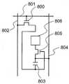
도 1a는, 기판(100) 위에 형성된 박막 트랜지스터(150)의 단면도를 도시한다. 박막 트랜지스터(150)는, 기판(100) 위에 형성된 게이트 전극층(101)과, 게이트 전극층(101) 위에 형성된 게이트 절연층(102)과, 게이트 절연층(102) 위에 형성된 산화물 반도체층(103)과, 산화물 반도체층(103) 위에 형성된 도전체인 한 쌍의 도전층(104a, 104b), 및 절연체 또는 반도체인 금속 산화물층(105)을 갖는 버퍼층(106)과, 도전층(104a)(한 쌍의 도전층(104a, 104b)의 한 쪽) 위에 형성된 소스 전극층(107a)과, 도전층(104b)(한 쌍의 도전층(104a, 104b)의 다른 쪽) 위에 형성된 드레인 전극층(107b)을 갖는다. 또한, 한 쌍의 도전층(104a, 104b)은, 산화물 반도체층(103)의 양단부 위에 형성되고, 금속 산화물층(105)은, 산화물 반도체층(103)의 중앙부 위에 형성된다.1A shows a cross-sectional view of a
바꾸어 말하면, 도 1a의 박막 트랜지스터(150)는, 산화물 반도체층(103)과 소스 전극층(107a) 및 드레인 전극층(107b) 사이에, 한 쌍의 도전층(104a, 104b) 및 금속 산화물층(105)이 형성된 버퍼층(106)을 갖는 역 스태거형의 박막 트랜지스터이다.1A includes a pair of
도 1b는, 기판 위에 형성된 박막 트랜지스터(151)의 단면도를 도시한다. 박막 트랜지스터(151)는, 도 1a에 도시한 박막 트랜지스터(150)의 구성에 더하여, 산화물 반도체층(103)의 양단부에 형성된 한 쌍의 산소 농도가 저하된 산화물 반도체층(108a, 108b)과, 한 쌍의 산소 농도가 저하된 산화물 반도체층(108a, 108b) 위에 형성된 한 쌍의 고농도로 산소를 함유하는 도전층(109a, 109b)을 갖는다.1B shows a cross-sectional view of a
바꾸어 말하면, 도 1b의 박막 트랜지스터(151)는, 산화물 반도체층(103)과 소스 전극층(107a) 및 드레인 전극층(107b) 사이에, 한 쌍의 도전층(104a, 104b), 금속 산화물층(105), 한 쌍의 산소 농도가 저하된 산화물 반도체층(108a, 108b), 및 한 쌍의 고농도로 산소를 함유하는 도전층(109a, 109b)이 형성된 버퍼층(110)을 갖는 역 스태거형의 박막 트랜지스터이다.1B includes a pair of
기판(100)으로서는, 바륨 보로실리케이트 유리나, 알루미노 보로실리케이트 유리 등의 유리 기판 등을 사용할 수 있다.As the
게이트 전극층(101)으로서는, 알루미늄(Al), 구리(Cu), 티타늄(Ti), 탄탈(Ta), 텅스텐(W), 몰리브덴(Mo), 크롬(Cr), 네오디뮴(Nd), 스칸듐(Sc)으로부터 선택된 원소, 상술한 원소를 성분으로 하는 합금, 또는 상술한 원소를 성분으로 하는 질화물을 적용할 수 있다. 또한, 이들의 재료의 적층 구조를 적용할 수도 있다.The
게이트 절연층(102)으로서는, 산화실리콘, 질화실리콘, 산화질화실리콘, 질화산화실리콘, 산화알루미늄, 산화탄탈 등의 절연체를 적용할 수 있다. 또한, 이들의 절연체로 이루어지는 적층 구조를 적용하여도 좋다. 또한, 산화질화실리콘이란 그 소성으로서, 질소보다도 산소의 함유량이 많은 것이고, 농도 범위로서 산소가 55at.% 내지 65at.%, 질소가 1at.% 내지 20at.%, 실리콘이 25at.% 내지 35at.%, 수소가 0.1at.% 내지 10at.% 범위에 있어서, 합계 100at.%가 되도록 각 원소를 임의의 농도로 포함하는 것을 가리킨다. 또한, 질화산화실리콘이란, 그 소성으로서 산소보다도 질소의 함유량이 많은 것이고, 농도 범위로서 산소가 15at.% 내지 30at.%, 질소가 20at.% 내지 30at.%, 실리콘이 25at.% 내지 35at.%, 수소가 15at.% 내지 25at.%의 범위에 있어서, 합계 100at.%가 되도록 각 원소를 임의의 농도로 포함하는 것을 가리킨다.As the
산화물 반도체층(103)으로서는, In-Ga-Zn-O계 산화물 반도체, In-Sn-Zn-O계 산화물 반도체, In-Zn-O계 산화물 반도체, Sn-Zn-O계 산화물 반도체, In-Sn-O계 산화물 반도체, Ga-Zn-O계 산화물 반도체, 또는, Zn-O계 산화물 반도체 등의 산화물 반도체를 적용할 수 있다. 또한, 이들의 산화물 반도체에 질소(N), 실리콘(Si)을 첨가한 산화물 반도체를 적용할 수도 있다. 또한, 이들의 재료의 적층 구조를 적용할 수도 있다.Zn-O-based oxide semiconductors, Sn-Zn-O-based oxide semiconductors, In-Zn-O-based oxide semiconductors, In- Sn-O-based oxide semiconductors, Ga-Zn-O-based oxide semiconductors, or Zn-O-based oxide semiconductors. An oxide semiconductor in which nitrogen (N) and silicon (Si) are added to these oxide semiconductors may also be applied. A laminated structure of these materials may also be applied.
한 쌍의 도전층(104a, 104b)으로서는, 티타늄(Ti), 구리(Cu), 아연(Zn), 알루미늄(Al) 등을 적용할 수 있다. 또한, 상술한 금속 원소를 갖는 합금을 적용할 수도 있다. 또한, 이들의 재료의 적층 구조를 적용할 수도 있다.As the pair of
금속 산화물(105)로서는, 한 쌍의 도전층(104a, 104b)과 같은 재료를 적용할 수 있다. 다만, 금속 산화물층(105)은, 한 쌍의 도전층(104a, 104b)보다도 산소 농도가 높다. 즉, 금속 산화물층(105)은, 한 쌍의 도전층(104a, 104b)과 같은 금속 원소를 갖고, 또한 도전층(104a, 104b)보다도 산소 농도가 높다.As the
소스 전극층(107a) 및 드레인 전극층(107b)으로서는, 알루미늄(Al), 구리(Cu), 티타늄(Ti), 탄탈(Ta), 텅스텐(W), 몰리브덴(Mo), 크롬(Cr), 네오디뮴(Nd), 스칸듐(Sc)으로부터 선택된 원소, 상술한 원소를 성분으로 하는 합금, 또는 상술한 원소를 성분으로 하는 질화물을 적용할 수 있다. 또한, 이들의 재료의 적층 구조를 적용할 수 있다.The
한 쌍의 산소 농도가 저하된 산화물 반도체층(108a, 108b)으로서는, 산화물 반도체층(103)과 같은 재료를 적용할 수 있다. 다만, 한 쌍의 산소 농도가 저하된 산화물 반도체층(108a, 108b)은, 산화물 반도체층(103)보다도 산소 농도가 낮다. 즉, 한 쌍의 산소 농도가 저하된 산화물 반도체층(108a, 108b)은, 산화물 반도체층(103)과 같은 금속 원소를 갖고, 또한, 산화물 반도체층(103)보다도 산소 농도가 낮다.As the
한 쌍의 고농도로 산소를 함유하는 도전층(109a, 109b)으로서는, 한 쌍의 도전층(104a, 104b) 및 금속 산화물층(105)과 같은 재료를 적용할 수 있다. 다만, 한 쌍의 고농도로 산소를 함유하는 도전층(109a, 109b)은, 한 쌍의 도전층(104a, 104b)보다도 산소 농도가 높고, 금속 산화물층(105)보다도 산소 농도가 낮다. 즉, 한 쌍의 고농도로 산소를 함유하는 도전층(109a, 109b)은, 한 쌍의 도전층(104a, 104b) 및 금속 산화물층(105)과 같은 금속 원소를 갖고, 또한, 도전층(104a, 104b)보다도 산소 농도가 높고, 금속 산화물층(105)보다도 산소 농도가 낮다.A material such as a pair of
도 1a에 도시한 박막 트랜지스터(150)는, 소스 전극층(107a) 및 드레인 전극층(107b)과 산화물 반도체층(103) 사이에 버퍼층(106)이 형성된다. 버퍼층(106)은, 산화물 반도체층(103)의 중앙부 위에, 절연체 또는 반도체인 금속 산화물층(105)을 갖는다. 금속 산화물층(105)은, 산화물 반도체층(103)의 불순물(수소 또는 물 등)에의 침입을 억제하는 보호층으로서 기능한다. 따라서, 박막 트랜지스터(150)의 오프 전류의 증가, 또는 임계값 전압의 마이너스 시프트를 예방할 수 있다.1A, the
도 1b에 도시한 박막 트랜지스터(151)의 버퍼층(110)은, 오프 전류의 증가, 또는 임계값 전압의 마이너스 시프트를 예방하는 금속 산화물층(105)과 함께, 산화물 반도체층(103)의 양단부 위에, 한 쌍의 산소 농도가 저하된 산화물 반도체층(108a, 108b)을 갖는다. 한 쌍의 산소 농도가 저하된 산화물 반도체층(108a, 108b)은, 산화물 반도체층(103)과 비교하여 저항이 낮다. 따라서, 소스 전극층(107a) 및 드레인 전극층(107b)과 산화물 반도체층(103)의 접합을 오믹 접합으로 할 수 있다.The
(실시형태 2)(Embodiment 2)
본 실시형태에서는, 실시형태 1에서 설명한 박막 트랜지스터의 제작 방법의 일례에 대해서 도 2a 내지 도 2d 및 도 3a 내지 도 3d를 사용하여 설명한다.In this embodiment mode, an example of a method of manufacturing a thin film transistor described in
또한, 본 실시형태에 있어서, "막"이란, 기판 전체면에 형성된 것이고, 후에 포토리소그래피 공정에 의하여 원하는 형상으로 가공되는 것이, 가공 전의 상태인 것을 가리킨다. 그리고, "층"이란, "막"으로부터 포토리소그래피 공정 등에 의하여 원하는 형상으로 가공, 형성된 것, 및 기판 전체면에 형성하는 것을 목적으로 한 것을 가리킨다.In the present embodiment, the term "film " means that the film is formed on the entire surface of the substrate and is processed beforehand by a photolithography process to a desired shape. The term "layer " refers to a process in which a film is processed and formed into a desired shape from a film, such as a photolithography process, and is formed on the entire surface of the substrate.
기판(200) 위에 제 1 도전막(201)을 형성한다. 제 1 도전막(201)의 형성에는, 스퍼터링법, 진공 증착법, 펄스 레이저 퇴적법, 이온 플레이팅(plating)법, 유기 금속 기상 성장법 등에 대표되는 박막 퇴적법을 사용할 수 있다. 이어서, 제 1 도전막(201) 위에 제 1 레지스트(202)를 형성한다. 여기까지의 공정을 마친 단계의 단면도가 도 2a에 상당한다.A first
이어서, 제 2 레지스트(202)를 마스크서, 제 1 도전막(201)을 선택적으로 에칭함으로써 게이트 전극층(203)을 형성한다. 또한, 기판(200) 및 제 1 도전막(201)(게이트 전극층(203))의 재료는, 실시형태 1에서 예를 든 재료를 사용할 수 있기 때문에, 여기서는 상술의 설명을 원용한다. 또한, 제 1 레지스트(202)는, 게이트 전극층(203) 형성 후에 제거한다. 여기까지의 공정을 마친 단계의 단면도가 도 2b에 상당한다.Then, the
이어서, 기판(200) 및 게이트 전극층(203) 위에 게이트 절연층(204)을 형성한다. 게이트 절연층(204)의 형성에는, 스퍼터링법, 진공 증착법, 펄스 레이저 퇴적법, 이온 플레이팅법, 유기 금속 기상 성장법, 플라즈마CVD법 등에 대표되는 박막 퇴적법을 사용할 수 있다.Then, a
이어서, 산화물 반도체막(205)을 형성한다. 산화물 반도체막(205)의 형성에는, 스퍼터링법, 진공 증착법, 펄스 레이저 퇴적법, 이온 플레이팅법, 유기 금속 기상 성장법 등에 대표되는 박막 퇴적법을 사용할 수 있다. In-Ga-Zn-O계 산화물 반도체를 스퍼터링법으로서 형성하는 경우, In2O3, Ga2O3, ZnO를 소결한 타깃을 사용하는 것이 바람직하다. 스퍼터 가스에는 아르곤에 대표되는 희 가스를 사용한다. 스퍼터링법에 의한 성막 조건의 하나는, In2O3: Ga2O3: ZnO=1: 1: 1을 혼합, 소결한 타깃을 사용하여, 압력 0.4Pa, 직류(DC) 전원 500W, 아르곤 가스 유량 30sccm, 산소 가스 유량을 15sccm로 하는 것이다. 또한, 산화물 반도체막(205) 성막 후에, 100℃ 내지 600℃, 대표적으로는 200℃ 내지 400℃의 열처리를 행하는 것이 바람직하다. 상기 열처리에 의하여 산화물 반도체의 원자 레벨의 재배치가 행해진다. 상기 열처리(광 어닐링 등도 포함함)는, 산화물 반도체막(205) 중에 있어서의 캐리어의 이동을 저해하는 변형을 해방할 수 있는 관점에서 중요하다.Then, an
이어서, 산화물 반도체막(205) 위에 제 2 도전막(206)을 형성한다. 제 2 도전막(206)의 형성에는, 스퍼터링법, 진공 증착법, 펄스 레이저 퇴적법, 이온 플레이팅법, 유기 금속 기상 성장법 등에 대표되는 박막 퇴적법을 사용한다. 제 2 도전막(206)의 재료로서는 티타늄(Ti), 구리(Cu), 아연(Zn), 알루미늄(Al) 등을 사용할 수 있다. 또한, 상술한 금속 원소를 갖는 합금을 사용할 수도 있다. 또한, 이들의 재료의 적층 구조를 사용할 수도 있다. 이어서, 제 2 도전막(206) 위에 제 2 레지스트(207)를 형성한다. 여기까지의 공정을 마친 단계의 단면도가 도 2c에 상당한다.Subsequently, a second
이어서, 제 2 레지스트(207)를 마스크로서, 산화물 반도체막(205) 및 제 2 도전막(206)을 선택적으로 에칭함으로써 산화물 반도체층(208) 및 도전층(209)을 형성한다. 또한, 게이트 절연층(204) 및 산화물 반도체막(205)(산화물 반도체층(208))의 재료는, 실시형태 1에서 예를 든 재료를 사용할 수 있기 때문에, 여기서는 상술의 설명을 원용한다. 또한, 제 2 레지스트(207)는, 산화물 반도체층(208) 및 도전층(209)을 형성 후에 제거한다. 여기까지의 공정을 마친 단면도가 도 2d에 상당한다.The
이어서, 게이트 절연층(204) 및 도전층(209) 위에 제 3의 도전막(210)을 형성한다. 제 3 도전막(210)의 형성에는, 스퍼터링법, 진공 증착법, 펄스 레이저 퇴적법, 이온 플레이팅법, 유기 금속 기상 성장법 등에 대표되는 박막 퇴적법을 사용할 수 있다. 이어서, 제 3 도전막(210) 위에 제 3의 레지스트(211a, 211b)를 형성한다. 여기까지의 공정을 마친 단면도가 도 3a에 상당한다.Then, a third
이어서, 제 3 레지스트(211a, 211b)를 마스크로서 제 3 도전막(210)을 선택적으로 에칭함으로써 소스 전극층(212a) 및 드레인 전극층(212b)을 형성한다. 또한, 상기 에칭 공정에 있어서, 소스 전극층(212a) 및 드레인 전극층(212b)과 중첩하지 않는 영역(노출부)의 도전층(209)도 일부 에칭되어, 소스 전극층(212a) 및 드레인 전극층(212b)과 중첩하지 않는 영역(노출부)에 오목부를 갖는 도전층(231)이 형성된다. 또한, 제 3 도전막(210)(소스 전극층(212a) 및 드레인 전극층(212b)의 재료는, 실시형태 1에서 예를 든 재료를 사용할 수 있기 때문에, 여기서는 상술의 설명을 원용한다. 여기까지의 공정을 마친 단계의 단면도가 도 3b에 상당한다.The
이어서, 제 3 레지스트(211a, 211b)를 마스크로서 산화 처리를 행한다. 상기 산화 처리로서는, 산화 분위기하에서의 열 산화 처리, 플라즈마 산화 처리, 산소 이온 주입 등을 사용할 수 있다. 또한, 산화 분위기하에서의 산화 처리를 행한 후에, 플라즈마 산화 처리를 행하는 등, 복수의 처리를 조합할 수도 있다. 또한, 열 산화 처리를 행하는 산화 분위기로서는, 전조 산소 분위기, 산소 및 희 가스의 혼합 분위기, 대기 분위기 등을 적용할 수 있다. 상기 산화 처리에 의하여, 산화물 반도체층(208) 위에 형성된 도전층(213)의 중앙부(노출부)가 산화되어, 절연체 또는 반도체인 금속 산화물층(214)이 형성된다. 또한, 금속 산화물층(214)의 형성에 따라, 한 쌍의 도전층(215a, 215b)이 산화물 반도체층(208)의 양단부 위에 형성된다. 구체적으로는, 소스 전극층(212a) 및 드레인 전극층(212b)과 중첩하는 영역(비노출부)의 도전층(213)은, 소스 전극층(212a) 및 드레인 전극층(212b) 및 제 3 레지스트(212a, 212b)에 의하여, 산화로부터 보호된다. 결과적으로, 한 쌍의 도전층(215a, 215b)가 잔존된다. 또한, 상기 산화 처리에 의하여 산화되는 영역의 체적은 증대한다. 즉, 금속 산화물층(214)의 체적은, 산화되기 전의 도전층(213)의 중앙부의 체적보다도 크다. 여기까지의 공정을 마친 단면도가 도 3c에 상당한다. 또한, 여기까지의 공정을 마친 단계에서 도 1a에 도시하는 박막 트랜지스터(150)가 완성된다.Then, an oxidation process is performed using the third resists 211a and 211b as masks. The oxidation treatment may be thermal oxidation treatment in an oxidizing atmosphere, plasma oxidation treatment, oxygen ion implantation, or the like. It is also possible to combine a plurality of treatments such as a plasma oxidation treatment after an oxidation treatment in an oxidizing atmosphere. As the oxidizing atmosphere for performing the thermal oxidation treatment, a precursor oxygen atmosphere, a mixed atmosphere of oxygen and diluent gas, an atmospheric atmosphere, and the like can be applied. The central portion (exposed portion) of the
또한, 본 실시형태의 박막 트랜지스터는, 도 1a, 도 3c에 도시한 구성에 한정되지 않는다. 구체적으로는, 도 1a, 도 3c에서는, 상기 산화 처리에 의하여, 소스 전극층(212a) 및 드레인 전극층(212b)과 중첩하지 않는 영역(중앙부)의 도전층(213)만이 산화되어, 금속 산화물층(214)이 형성된 박막 트랜지스터를 도시하지만, 그 이외의 영역이 산화된 박막 트랜지스터도 본 실시형태의 박막 트랜지스터에는 포함된다. 예를 들어, 상기 산화 처리에 의하여, 제 3 레지스트(211a, 211b)로 덮이지 않는 소스 전극층(212a) 및 드레인 전극층(212b)의 측부가 산화된 박막 트랜지스터도 본 실시형태의 박막 트랜지스터에 포함된다. 또한, 소스 전극층(212a) 및 드레인 전극층(212b)의 측부가 산화되는 경우, 상기 산화를 측부 표면 영역에 고정시킴으로써, 소스 전극층(212a) 및 드레인 전극층(212b)을 전극으로서 기능시킬 수 있다. 마찬가지로, 상기 산화 처리에 의하여, 소스 전극층(212a) 및 드레인 전극층(212b)과 중첩하는 영역(비노출부)의 도전층(213)의 일부가 내부 산화된 박막 트랜지스터도 본 실시형태의 박막 트랜지스터에 포함된다.The thin film transistor of the present embodiment is not limited to the structure shown in Figs. 1A and 3C. Specifically, in FIG. 1A and FIG. 3C, only the
또한, 도 1a, 도 3c에서는, 상기 산화 처리에 의하여 형성된, 금속 산화물층(214)의 막 두께가 한 쌍의 도전층(215a, 215b)의 막 두께보다도 두꺼운 박막 트랜지스터를 도시하지만, 금속 산화물층(214)의 막 두께가 한 쌍의 도전층(215a, 215b)의 막 두께보다도 얇은 박막 트랜지스터도 본 실시형태의 박막 트랜지스터에 포함된다. 또한, 금속 산화물층(214)은, 오목부를 갖는 도전층(213)에 대해서 산화 처리를 행함으로써 형성된다. 또한, 상기 오목부는, 소스 전극층(212a) 및 드레인 전극층(212b)을 형성하는 에칭 공정시에, 형성된다. 즉, 소스 전극층(212a) 및 드레인 전극층(212b)을 형성하는 에칭 공정의 조건을 제어함으로써, 금속 산화물층(214)의 막 두께를 제어할 수 있다. 구체적으로는, 소스 전극층(212a) 및 드레인 전극층(212b)의 형성시의 오버 에칭 시간을 길게 함으로써, 상기 오목부를 깊게 할 수 있다. 따라서, 금속 산화물층(214)의 막 두께를 한 쌍의 도전층(215a, 215b)의 막 두께보다 얇게 할 수 있다.1A and 3B show a thin film transistor formed by the oxidation treatment, in which the film thickness of the
도 1b에 도시한 박막 트랜지스터(151)를 제작하는 경우는, 이어서, 100℃ 내지 600℃, 대표적으로는 200℃ 내지 400℃의 열처리를 행한다. 상기 열처리에 의하여, 산화물 반도체층(208) 중의 산소가 한 쌍의 도전층(215a, 215b)으로 확산된다. 또한, 상기 산소의 한 쌍의 도전층(215a, 215b)의 확산과, 금속 산화물층(214)의 확산을 비교한 경우, 한 쌍의 도전층(215a, 215b)으로 확산하는 산소량이 더 많다. 따라서, 산화물 반도체층(208)의 양단부 위에 한 쌍의 산소 농도가 저하된 산화물 반도체층(216a, 216b)이 형성되고, 한 쌍의 산소 농도가 저하된 산화물 반도체층(216a, 216b) 위에 한 쌍의 고농도로 산소를 함유하는 도전층(217a, 217b)이 형성된다. 그 후, 제 3 레지스트(211a, 212b)를 제거한다. 여기까지의 공정을 마친 단면도가 도 3d에 상당한다.In the case of fabricating the
여기서는, 도 1b에 도시한 박막 트랜지스터(151)를 제작하는 경우에 행하는 열처리를 산화 처리 후에 행하는 제작 공정을 나타냈지만, 상기 열처리의 타이밍은, 제 2 도전막(206) 형성 후라면, 어느 타이밍이라도 행하는 것이 가능하다. 또한, 상기 열처리는, 상술한 산화물 반도체층(208)의 원자 레벨의 재배치를 위한 열처리를 겸할 수 있다.Here, the fabrication process of performing the heat treatment performed in the case of fabricating the
또한, 형성되는 박막 트랜지스터의 특성이라는 관점에서 보면, 산화 처리 후에 열처리를 행하는 것이 바람직하다. 산화 처리를 행하기 전(금속 산화물층(214) 형성하기 전)에 열처리를 행하면, 산화물 반도체층(208)의 상방 양단부만이 아니라, 상부 전체에 산소 농도가 저하된 산화물 반도체층이 형성되고, 형성되는 박막 트랜지스터의 오프 전류가 증가하기 때문이다.From the viewpoint of the characteristics of the thin film transistor to be formed, it is preferable to perform the heat treatment after the oxidation treatment. When the heat treatment is performed before the oxidation treatment (before the formation of the metal oxide layer 214), an oxide semiconductor layer whose oxygen concentration is lowered is formed not only on both the upper and opposite ends of the
또한, 제작 공정이라는 관점에서 보면, 상술한 산화 처리로서, 한 쌍의 산소 농도가 저하된 산화물 반도체층(216a, 216b), 및 한 쌍의 고농도로 산소를 함유하는 도전층(217a, 217b)이 형성되는 온도에서의 산화 분위기하에서의 열 산화 처리를 행하는 것이 바람직하다. 금속 산화물층(214), 산소 농도가 저하된 산화물 반도체층(216a, 216b), 및 고농도로 산소를 함유하는 도전층(217a, 217b)를 동일 공정으로 형성할 수 있기 때문이다. 상기 산화 처리 및 상기 열처리를 겸하는 처리 조건의 하나는, 건조 산소 분위기하에서 350℃, 1시간의 열 산화 처리이다.In view of the fabrication process, the
또한, 형성되는 박막 트랜지스터의 신뢰성이라는 관점에서 보면, 열 산화 처리와 산화 처리를 조합하여 행하는 것이 바람직하다. 금속 산화물층(214)의 막 두께를 두껍게 함으로써, 산화물 반도체층(208)으로 불순물(수소 또는 물 등)의 침입을 억제하는 보호층으로서의 기능을 향상시킬 수 있기 때문이다.From the viewpoint of the reliability of the thin film transistor to be formed, it is preferable to perform the thermal oxidation treatment and the oxidation treatment in combination. This is because, by increasing the thickness of the
박막 트랜지스터(150)는, 산화물 반도체층(208)과 동일 공정으로 형성되는 도전층(209)(도전층(213))을 기초하여, 오프 전류의 증가, 또는 임계값 전압의 마이너스 시프트를 예방하는 기능을 갖는 금속 산화물층(214)이 형성되기 때문에, 효율 좋게 고성능의 박막 트랜지스터를 형성할 수 있다. 마찬가지로, 박막 트랜지스터(151)는, 산화물 반도체층(208)과 동일 공정으로 형성되는 도전층(209)(도전층(213))을 기초하여, 오프 전류의 증가, 또는 임계값 전압의 마이너스 시프트를 예방하는 기능을 갖는 금속 산화물층(214)이 형성되어, 또는 산화물 반도체층(208)과, 소스 전극층(212a) 및 드레인 전극층(212b)을 오믹 접합으로 하는 기능을 갖는 한 쌍의 산소 농도가 저하된 산화물 반도체층(216a, 216b)이, 한 쌍의 도전층(215a, 215b)으로 산소가 확산됨으로써 형성되기 때문에, 효율 좋게 고성능의 박막 트랜지스터를 형성할 수 있다.The
(실시형태 3)(Embodiment 3)
본 실시형태에서는, 실시형태 1에서 설명한 박막 트랜지스터를 사용한 반도체 장치의 일례를 나타낸다. 구체적으로는, 상기 박막 트랜지스터를 액티브 매트릭스 기판의 화소부에 형성되는 박막 트랜지스터에 적용한 액정 표시 장치에 대해서 도 4 내지 도 6에 도시한다. 이어서, 상기 액정 표시 장치에 대해서 설명한다.This embodiment shows an example of a semiconductor device using the thin film transistor described in the first embodiment. Specifically, a liquid crystal display device in which the thin film transistor is applied to a thin film transistor formed in a pixel portion of an active matrix substrate is shown in Figs. 4 to 6. Fig. Next, the liquid crystal display device will be described.
또한, 반도체 장치 내에 있어서, 박막 트랜지스터의 소스 및 드레인은, 동작 조건 등에 의하여 서로 바꾸기 때문에, 어느 것이 소스 또는 드레인인지를 특정하는 것이 어렵다. 그래서, 본 실시형태 이후에 있어서는, 소스 전극층 및 드레인 전극층의 한쪽을 제 1 전극층, 소스 전극층 및 드레인 전극층의 다른 쪽을 제 2 전극층이라고 표기하여, 구별하도록 한다.Further, in the semiconductor device, since the source and the drain of the thin film transistor change depending on operating conditions and the like, it is difficult to specify which is the source or the drain. Therefore, after this embodiment mode, one of the source electrode layer and the drain electrode layer is referred to as a first electrode layer, and the other of the source electrode layer and the drain electrode layer is referred to as a second electrode layer.
도 4는, 액티브 매트릭스 기판의 1화소를 도시하는 상면도이다. 본 실시형태의 액정 표시 장치의 화소는, 3개의 부화소에 의하여 구성된다. 각각 부화소에는, 박막 트랜지스터(300) 및 액정층에 전압을 인가하는 화소 전극(301)이 형성된다. 실시형태 1에서 나타낸 박막 트랜지스터는, 도 4 중의 박막 트랜지스터(300)에 적용할 수 있다. 화소부에는, 상술한 화소가 복수 형성된다. 또한, 복수의 게이트 배선(302), 복수의 소스 배선(303), 복수의 용량 배선(304)이 형성된다.4 is a top view showing one pixel of the active matrix substrate. The pixel of the liquid crystal display device of this embodiment is constituted by three sub-pixels. In each sub-pixel, a
도 5는, 도 4의 A-B선에 대응하는 단면도이다. 도 5에 포함되는 박막 트랜지스터(450)는, 도 1a에 도시한 박막 트랜지스터이다. 즉, 박막 트랜지스터(450)는, 기판(400) 위에 형성된 게이트 전극층(401)과, 게이트 전극층(401) 위에 형성된 게이트 절연층(402)과, 게이트 절연층(402) 위에 형성된 산화물 반도체층(403)과, 산화물 반도체층(403) 위에 형성된 한 쌍의 도전층(404a, 404b) 및 금속 산화물층(405)을 갖는 버퍼층(406)과, 도전층(404a) 위에 형성된 제 1 전극층(407a)과, 도전층(404b) 위에 형성된 제 2 전극층(407b)을 갖는 박막 트랜지스터이다.5 is a cross-sectional view corresponding to line A-B in Fig. The
기판(400) 내지 제 1 전극층(407a) 및 제 2 전극층(407b)에 적용 가능한 재료 및 제작 방법은, 실시형태 1에서 설명한 재료 및 실시형태 2에서 설명한 제작 방법을 사용할 수 있기 때문에, 여기서는 상술의 설명을 원용한다.The material and the manufacturing method applicable to the
또한, 부화소는 용량 소자(451)를 갖는다. 용량 소자(451)는, 박막 트랜지스터(450)의 게이트 전극층(401)과 동일 재료인 용량 배선(408)과, 게이트 절연층(402)과, 부화소에 연재하는 박막 트랜지스터(450)의 제 2 전극층(407b)에 의하여 구성된다.In addition, the sub-pixel has a
박막 트랜지스터(450) 및 용량 소자(451) 위에는, 층간 절연층(409)이 형성된다. 도 5에 도시하는 박막 트랜지스터(450)에는, 산화물 반도체층(403)으로 불순물(수소 또는 물 등)의 침입을 억제하는 금속 산화물층(405)이 형성되기 때문에, 층간 절연층(409)으로서 각종 재료, 제작 방법을 적용할 수 있다. 예를 들어, 층간 절연층(409)으로서, 플라즈마 CVD법이나 스퍼터링법을 사용하여, 산화실리콘층, 산화질화실리콘층, 질화실리콘층, 또는 질화산화실리콘층 등을 형성할 수 있다. 또한, 폴리이미드, 폴리아미드, 폴리비닐페놀, 벤조시클로부텐, 아크릴 또는 에폭시 등의 유기 재료, 실록산 수지 등의 실록산 재료, 또는 옥사졸 수지 등을 사용하여, 스핀 코팅법 등의 도포법에 의하여 형성할 수 있다. 또한, 실록산 재료란, Si-O-Si결합을 포함하는 재료에 상당한다. 실록산은, 실리콘(Si)과 산소(O)의 결합으로 골격 구조가 구성된다. 치환기로서, 유기기(예를 들어 알킬기, 방향족 탄화수소)나 플루오르기를 사용하여도 좋다. 유기기는, 플루오르기를 가져도 좋다. 또한, 층간 절연층(409)에 형성된 콘택트 홀(410)에 있어서, 박막 트랜지스터(450)의 제 2 전극층(407b)이 화소 전극(411)과 전기적으로 접속된다.On the
도 6은, 도 4의 부화소에 대응하는 등가 회로도이다. 박막 트랜지스터(500)의 게이트 전극은 게이트 배선(501)에 전기적으로 접속되고, 제 1 전극은 소스 배선(502)에 전기적으로 접속된다. 용량 소자(503)의 한쪽의 전극은 박막 트랜지스터(500)의 제 2 전극에 전기적으로 접속되고, 다른 전극은 용량 배선(504)에 전기적으로 접속된다. 화소 전극을 통하여 전압이 인가되는 액정층(505)은, 박막 트랜지스터(500)의 제 2 전극 및 용량 소자(503)의 한쪽 전극에 전기적으로 접속된다.6 is an equivalent circuit diagram corresponding to the sub-pixel of Fig. The gate electrode of the
액정 표시 장치는, 액티브 매트릭스 기판과, 표면에 대향 전극이 형성된 대향 기판에 의하여 협지된 액정층을 갖는다. 액정층을 구성하는 액정 분자는, 액티브 매트릭스 기판의 화소 전극 및 대향 기판의 대향 전극 사이에 인가되는 전압에 의하여 배향이 제어된다. 액정 표시 장치는, 상기 액정층이 배향함으로써, 백 라이트로부터의 광을 투과 또는 차광함으로써, 화상의 표시를 행한다. 액정 표시 장치에 있어서, 액티브 매트릭스 기판의 화소부의 박막 트랜지스터는, 액정층에 인가되는 전압을 제어하는 스위칭 소자이다.The liquid crystal display device has an active matrix substrate and a liquid crystal layer sandwiched by an opposing substrate on which a counter electrode is formed. The orientation of the liquid crystal molecules constituting the liquid crystal layer is controlled by the voltage applied between the pixel electrode of the active matrix substrate and the opposing electrode of the counter substrate. The liquid crystal display device displays an image by orienting the liquid crystal layer so as to transmit or shield light from the backlight. In the liquid crystal display device, the thin film transistor in the pixel portion of the active matrix substrate is a switching element for controlling the voltage applied to the liquid crystal layer.
본 실시형태의 액정 표시 장치는, 산화물 반도체층(403) 위에 금속 산화물층(405)이 형성된 박막 트랜지스터(450)를 액티브 매트릭스 기판의 화소부의 박막 트랜지스터로서 사용한다. 금속 산화물층(405)은, 산화물 반도체층(403)으로 불순물(수소 또는 물 등)의 침입을 억제하는 보호층으로서 기능한다. 따라서, 목적에 따라, 층간 절연막(409)의 재료, 제작 방법을 선택할 수 있다. 결과적으로, 고품질, 또는 고신뢰성의 액정 표시 장치를 제공할 수 있다. 또한 여기서는 도 1a에 도시한 박막 트랜지스터를 적용한 액정 표시 장치에 대해서 나타냈지만, 도 1b에 도시한 박막 트랜지스터를 적용한 경우도 같은 효과를 나타낸다.The liquid crystal display device of this embodiment uses the
(실시형태 4)(Fourth Embodiment)
본 실시형태에서는, 실시형태 1에서 설명한 박막 트랜지스터를 사용한 반도체 장치의 일례를 나타낸다. 구체적으로는, 상기 박막 트랜지스터를 액티브 매트릭스 기판의 화소부에 형성되는 박막 트랜지스터에 적용한 발광 표시 장치에 대해서 도 7 내지 도 9에 도시한다. 이어서, 본 실시형태의 발광 표시 장치에 대해서 설명한다. 또한, 본 실시형태의 발광 표시 장치가 갖는 표시 소자로서 여기서는 일렉트로 루미네선스를 활용하는 발광 소자를 사용하여 나타낸다. 일렉트로 루미네선스를 활용하는 발광 소자는, 발광 재료가 유기 화합물인지 무기 화합물인지에 따라 구별되고, 일반적으로 전자는 유기 EL소자, 후자는 무기 EL소자라고 불린다.This embodiment shows an example of a semiconductor device using the thin film transistor described in the first embodiment. Specifically, a light emitting display device in which the thin film transistor is applied to a thin film transistor formed in a pixel portion of an active matrix substrate is shown in FIGS. 7 to 9. FIG. Next, the light emitting display device of the present embodiment will be described. Here, as a display element of the light emitting display device of the present embodiment, here, a light emitting element utilizing electroluminescence is used. The light emitting element utilizing the electroluminescence is classified according to whether the light emitting material is an organic compound or an inorganic compound, and the former is generally called an organic EL element and the latter is called an inorganic EL element.
유기 EL 소자는 발광 소자에 전압을 인가함으로써, 한 쌍의 전극으로부터 전자 및 정공이 각각 발광성의 유기 화합물을 함유한 층에 주입되어 전류가 흐른다. 그리고, 이들 캐리어(전자 및 정공)가 재결합함으로써, 발광성의 유기 화합물이 여기 상태를 형성하고, 그 여기 상태가 기저 상태로 되돌아올 때 발광한다. 이러한 메커니즘에 의하여, 이러한 발광 소자는 전류 여기형의 발광 소자라고 불린다.In the organic EL element, electrons and holes from a pair of electrodes are injected into a layer containing a luminescent organic compound by applying a voltage to the luminescent element, and a current flows. These carriers (electrons and holes) are recombined to emit light when the organic compound of luminescence forms an excited state and the excited state returns to the ground state. By such a mechanism, such a light-emitting element is called a current-excited light-emitting element.
무기 EL 소자는 그 소자 구성에 의하여, 분산형 무기 EL 소자와 박막형 무기 EL 소자로 분류된다. 분산형 무기 EL 소자는 발광 재료의 입자를 바인더 중에 분산시킨 발광층을 갖는 것이고, 발광 메커니즘은 도너 준위와 억셉터 준위를 활용하는 도너-억셉터 재결합형 발광이다. 박막형 무기 EL 소자는 발광층을 유전체층으로 끼우고, 또한 그것을 전극으로 끼운 구조이며, 발광 메커니즘은 금속 이온의 내각(內殼) 전자 천이를 활용하는 국재(局在)형 발광이다. 또한, 여기서는, 발광 소자로서 유기 EL 소자를 사용하여 설명한다.The inorganic EL element is classified into a dispersion type inorganic EL element and a thin film inorganic EL element by its element structure. The dispersion-type inorganic EL device has a light-emitting layer in which particles of a light-emitting material are dispersed in a binder, and the light-emitting mechanism is a donor-acceptor recombination-type light-emitting utilizing a donor level and an acceptor level. The thin film type inorganic EL device is a structure in which a light emitting layer is sandwiched between dielectric layers and sandwiched therebetween, and the light emitting mechanism is localized light emission utilizing the internal transition of metal ions. Here, an organic EL element is used as a light emitting element.
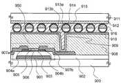
도 7은, 액티브 매트릭스 기판의 1화소에 도시하는 상면도이다. 본 실시형태의 발광 표시 장치의 화소는, 3개의 부화소에 의하여 구성된다. 각각 부화소에는, 박막 트랜지스터(600, 601), 발광 소자에 전압을 인가하는 화소 전극(602)이 형성되다(편의상 화소 전극(602)의 일부는 도시하지 않음). 실시형태 1에서 나타낸 박막 트랜지스터는, 도 6 중의 박막 트랜지스터(600, 601)에 적용할 수 있다. 화소부에는, 상술한 화소가 복수 형성된다. 또한, 복수의 게이트 배선(603), 복수의 소스 배선(604), 복수의 전원선(605)이 형성된다. 또한, 전원선(605) 위에는, 고전원 전위 VDD가 설정된다.7 is a top view of one pixel of the active matrix substrate. The pixel of the light emitting display device of the present embodiment is composed of three sub-pixels. In each sub-pixel,
도 8은, 도 7의 C-D선, E-F선에 대응하는 단면도이다. 박막 트랜지스터(750, 751)는, 도 1a에 도시한 박막 트랜지스터이다. 즉, 박막 트랜지스터(750, 751)는, 기판(700) 위에 형성된 게이트 전극층(701)과, 게이트 전극층(701) 위에 형성된 게이트 절연층(702)과, 게이트 절연층(702) 위에 형성된 산화물 반도체층(703)과, 산화물 반도체층(703) 위에 형성된, 도전층(704a, 704b) 및 금속 산화물층(705)을 갖는 버퍼층(706)과, 도전층(704a) 위에 형성된 제 1 전극층(707a)과, 도전층(704b) 위에 형성된 제 2 전극층(707b)을 갖는 박막 트랜지스터이다.8 is a cross-sectional view corresponding to line C-D and line E-F in Fig. The
기판(700) 내지 제 1 전극층(707a) 및 제 2 전극층(707b)에 적용 가능한 재료 및 제작 방법은, 실시형태 1에서 설명한 재료 및 실시형태 2에서 설명한 제작 방법을 사용할 수 있기 때문에 여기서는 상술한 설명을 원용한다.The material and the manufacturing method applicable to the
또한, 부화소는 용량 소자(752)를 갖는다. 용량 소자(752)는, 박막 트랜지스터(750, 751)의 게이트 전극층(701)과 동일 재료인 용량 배선(708)과, 게이트 절연층(702)과, 부화소에 연재하는 박막 트랜지스터(751)의 제 1 전극층(707a)에 의하여 구성된다.In addition, the sub-pixel has the
박막 트랜지스터(750, 751) 및 용량 소자(752) 위에는, 층간 절연층(709)이 형성된다. 도 8에 도시하는 박막 트랜지스터(750, 751)에는, 산화물 반도체층(703)으로 불순물(수소 또는 물 등)의 침입을 억제하는 금속 산화물층(705)이 형성되기 때문에, 층간 절연층(709)으로서 각종 재료, 제작 방법을 적용할 수 있다. 예를 들어, 층간 절연층(709)으로서, 플라즈마 CVD법이나 스퍼터링법을 사용하여, 산화실리콘층, 산화질화실리콘층, 질화실리콘층, 또는 질화산화실리콘층 등을 형성할 수 있다. 또한, 폴리이미드, 폴리아미드, 폴리비닐페놀, 벤조시클로부텐, 아크릴 또는 에폭시 등의 유기 재료, 실록산 수지 등의 실록산 재료, 또는 옥사졸 수지 등을 사용하여, 스핀 코팅법 등의 도포법에 의하여 형성할 수 있다. 또한, 실록산 재료란, Si-O-Si결합을 포함하는 재료에 상당한다. 실록산은, 실리콘(Si)과 산소(O)의 결합으로 골격 구조가 구성된다. 치환기로서, 유기기(예를 들어 알킬기, 방향족 탄화수소)나 플루오르기를 사용하여도 좋다. 유기기는, 플루오르기를 가져도 좋다. 또한, 층간 절연층(709)에는, 복수의 콘택트 홀(710a, 710b, 710c)이 형성된다. 박막 트랜지스터(751)의 제 2 전극층(707b)는, 콘택트 홀(710c)에 있어서, 화소 전극(711)과 전기적으로 접속된다.An interlayer insulating
도 9는, 도 7의 부화소에 대응하는 등가 회로도이다. 박막 트랜지스터(800)의 게이트 전극은 게이트 배선(801)에 전기적으로 접속되고, 제 1 전극은 소스 배선(802)에 전기적으로 접속된다. 용량 소자(803)의 한쪽의 전극은 박막 트랜지스터(800)의 제 2 전극에 전기적으로 접속되고, 다른 전극은 전원선(804)에 전기적으로 접속된다. 박막 트랜지스터(805)의 게이트 전극은 박막 트랜지스터(800)의 제 2 전극에 전기적으로 접속되고, 제 1 전극은 전원선(804) 및 용량 소자(803)의 다른 측의 전원에 접속된다. 화소 전극을 통하여 전압이 인가되는 유기 EL소자(806)는, 박막 트랜지스터(805)의 제 2 전극에 전기적으로 접속된다.9 is an equivalent circuit diagram corresponding to the sub-pixel of FIG. The gate electrode of the
발광 표시 장치는, 액티브 매트릭스 기판의 화소 전극 위에 형성된 유기 EL소자와, 상기 유기 EL소자 위에 형성된 공통 전극을 갖는다. 또한, 공통 전극에는 저전원 전위 VSS가 설정된다. 상기 유기 EL소자는, 박막 트랜지스터를 통하여 화소 전극에 주어지는 고전원 전위 VDD와, 공통 전극에 주어지는 저전원 전위 VSS의 전위 차분의 전압이 인가되었을 때 전류가 흘러, 발광한다. 발광 표시 장치에 있어서, 액티브 매트릭스 기판의 화소부의 박막 트랜지스터는, 유기 EL소자에 흐르는 전류를 제어하는 스위칭 소자이다.The light emitting display device has an organic EL element formed on the pixel electrode of the active matrix substrate and a common electrode formed on the organic EL element. Also, a low power supply electric potential VSS is set to the common electrode. The organic EL element emits light when a voltage of a potential difference between a high power supply potential VDD applied to the pixel electrode through the thin film transistor and a low power supply potential VSS applied to the common electrode flows. In the light emitting display, the thin film transistor in the pixel portion of the active matrix substrate is a switching element that controls the current flowing in the organic EL element.
본 실시형태의 발광 표시 장치는, 산화물 반도체층(703) 위에 금속 산화물층(705)이 형성된 박막 트랜지스터(750, 751)를 액티브 매트릭스 기판의 화소부의 박막 트랜지스터로서 사용한다. 금속 산화물층(705)은, 산화물 반도체층(703)으로 불순물(수소 또는 물 등)의 침입을 억제하는 보호층으로서 기능한다. 따라서, 목적에 따라, 층간 절연막(709)의 재료, 제작 방법을 선택할 수 있다. 결과적으로, 고품질, 또는 고신뢰성의 발광 표시 장치를 제공할 수 있다. 또한 여기서는 도 1a에 도시한 박막 트랜지스터를 적용한 발광 표시 장치에 대해서 나타냈지만, 도 1b에 도시한 박막 트랜지스터를 적용한 경우도 같은 효과를 나타낸다.The light emitting display device of the present embodiment uses the
(실시형태 5)(Embodiment 5)
본 실시형태에서는, 실시형태 1에서 설명한 박막 트랜지스터를 사용한 반도체 장치의 일례를 나타낸다. 구체적으로는, 상기 박막 트랜지스터를 액티브 매트릭스 기판에 형성되는 박막 트랜지스터에 적용한 전자 페이퍼에 대해서 도 10에 도시한다. 이어서, 본 실시형태의 전자 페이퍼에 대해서 설명한다.This embodiment shows an example of a semiconductor device using the thin film transistor described in the first embodiment. Specifically, FIG. 10 shows an electronic paper in which the thin film transistor is applied to a thin film transistor formed on an active matrix substrate. Next, the electronic paper of this embodiment will be described.
도 10은, 액티브 매트릭스형의 전자 페이퍼의 단면도이다. 제 1 기판(액티브 매트릭스 기판)(900) 위에 형성된 박막 트랜지스터(950)는, 도 1a에 도시한 박막 트랜지스터이다. 즉, 박막 트랜지스터(950)는, 제 1 기판(900) 위에 형성된 게이트 전극층(901)과, 게이트 전극층(901) 위에 형성된 게이트 절연층(902)과, 게이트 절연층(902) 위에 형성된 산화물 반도체층(903)과, 산화물 반도체층(903) 위에 형성된, 한 쌍의 도전층(904a, 904b) 및 금속 산화물층(905)을 갖는 버퍼층(906)과, 도전층(904a) 위에 형성된 제 1 전극층(907a)과, 도전층(904a) 위에 형성된 제 2 전극층(907b)을 갖는 박막 트랜지스터이다.10 is a cross-sectional view of an active matrix type electronic paper. The
기판(900) 내지 제 1 전극층(907a) 및 제 2 전극층(907b)에 적용 가능한 재료 및 제작 방법은, 실시형태 1에서 설명한 재료 및 실시형태 2에서 설명한 제작 방법을 사용할 수 있기 때문에, 여기서는 상술한 설명을 원용한다.Materials and fabrication methods applicable to the
박막 트랜지스터(950) 위에는, 층간 절연층(908)이 형성된다. 도 10에 도시하는 박막 트랜지스터(950)에는, 산화물 반도체층(903)의 불순물(수소 또는 물 등)의 침입을 억제하는 금속 산화물층(905)이 형성되기 때문에, 층간 절연층(908)으로서 각종 재료, 제작 방법을 적용할 수 있다. 예를 들어, 층간 절연층(908)으로서, 플라즈마 CVD법이나 스퍼터링법을 사용하여, 산화실리콘층, 산화질화실리콘층, 질화실리콘층, 또는 질화산화실리콘층 등을 형성할 수 있다. 또한, 폴리이미드, 폴리아미드, 폴리비닐페놀, 벤조시클로부텐, 아크릴 또는 에폭시 등의 유기 재료, 실록산 수지 등의 실록산 재료, 또는 옥사졸 수지 등을 사용하여, 스핀 코팅법 등의 도포법에 의하여 형성할 수 있다. 또한, 실록산 재료란, Si-O-Si결합을 포함하는 재료에 상당한다. 실록산은, 실리콘(Si)과 산소(O)의 결합으로 골격 구조가 구성된다. 치환기로서, 유기기(예를 들어 알킬기, 방향족 탄화수소)나 플루오르기를 사용하여도 좋다. 유기기는, 플루오르기를 가져도 좋다. 또한, 층간 절연층(908)에는 콘택트 홀(909)이 형성된다. 박막 트랜지스터(950)의 제 2 전극층(907b)는, 콘택트 홀(909)에 있어서, 화소 전극(910)과 전기적으로 접속된다.On the
화소 전극(910)과 제 2 기판(911) 위에 형성된 공통 전극(912) 사이에는, 흑색 영역(913a) 및 백색 영역(913b)을 갖고, 주위에 액체로 채워져 있는 캐비티(914)를 포함하는 트위스트 볼(915)이 형성된다. 또한, 트위스트 볼(915)의 주위는 수지 등의 충전재(916)로 충전된다.A
본 실시형태의 전자 페이퍼는, 트위스트 볼 표시방식을 사용한다. 상기 전자 페이퍼는, 백색과 흑색으로 나누어 칠해진 트위스트 볼을 화소 전극 및 공통 전극 사이에 갖는다. 트위스트 볼은, 제 1 기판의 화소 전극 및 제 2 기판의 공통 전극 사이에 인가되는 전압에 의하여 방향이 제어됨으로써, 표시를 행한다. 전자 페이퍼에 있어서, 액티브 매트릭스 기판의 박막 트랜지스터는, 트위스트 볼에 인가되는 전압을 제어하는 스위칭 소자이다.The electronic paper of this embodiment uses a twisted ball display system. The electronic paper has a twisted ball divided into a white color and a black color between the pixel electrode and the common electrode. The direction of the twisted ball is controlled by the voltage applied between the pixel electrode of the first substrate and the common electrode of the second substrate, thereby performing display. In the electronic paper, the thin film transistor of the active matrix substrate is a switching element for controlling the voltage applied to the twist ball.
본 실시형태의 발광 표시 장치는, 산화물 반도체층(903) 위에 금속 산화물층(905)이 형성된 박막 트랜지스터(950)를 액티브 매트릭스 기판의 박막 트랜지스터로서 사용한다. 금속 산화물층(905)은, 산화물 반도체층(903)으로 불순물(수소 또는 물 등)의 침입을 억제하는 보호층으로서 기능한다. 따라서, 목적에 따라, 층간 절연층(908)의 재료, 제작 방법을 선택할 수 있다. 결과적으로, 고품질, 또는 고신뢰성의 전자 페이퍼를 제공할 수 있다. 또한, 여기서는 도 1a에 도시한 박막 트랜지스터를 적용한 전자 페이퍼에 대해서 나타냈지만, 도 1b에 도시한 박막 트랜지스터를 적용한 경우도 같은 효과를 나타낸다.The light emitting display device of this embodiment uses the
여기서는, 산소 함유량의 차이에 의한 티타늄 및 티탄산화물의 전자 형상의 변화, 산화물 반도체층의 산소 결손에 따른 전자 상태의 변화, 열처리를 하는 데에 있어서의 티타늄층 및 산화물 반도체층의 접합 계면 근방에 있어서의 산소의 거동, 및 열처리를 하는 데에 있어서의 티탄산화물층 및 산화물 반도체층의 접합 계면 근방에 있어서의 산소의 거동에 관한 계산 결과를 나타낸다. 이어서, 버퍼층의 구성 재료에 티타늄을 적용한 실시형태 1의 박막 트랜지스터에 대해서 검증한다.Here, in the vicinity of the junction interface between the titanium layer and the oxide semiconductor layer in the change of the electron shape of the titanium and titanium oxide due to the difference in the oxygen content, the change of the electron state due to the oxygen deficiency of the oxide semiconductor layer, And the behavior of oxygen in the vicinity of the bonding interface between the titanium oxide layer and the oxide semiconductor layer in the heat treatment. Then, the thin film transistor of
우선, 산소 함유량의 차이에 의한 티타늄 및 티탄산화물의 전자 상태의 변화를 검증한다. 여기서는, 티타늄 및 복수의 티탄산화물의 결정 구조의 에너지 상태 밀도를 밀도 범함수(密度汎函數) 이론(Density Functional Theory: DFT)에 의거하는 평면파-의사포텐셜법(plane wave-pseudopotential method)을 사용한 제 1 원리 계산에 의한 구조 최적화에 의하여 구한 결과에 대해서 나타낸다. 구체적으로는, Ti, TiO(NaCl형), Ti2O3(Al2O3형), TiO2(Anatase형), TiO2(Rutile형), 및 TiO2(Brookite형)의 구조를 최적화한 후의 상태 밀도도를 나타낸다. 또한, 계산 프로그램으로서는 CASTEP를, 교환상관 범함수로서는 GGA-PBE를 사용하였다.First, the change in the electronic state of titanium and titanium oxide due to the difference in oxygen content is verified. Here, the energy state density of the crystal structure of titanium and a plurality of titanium oxides is determined by using a plane wave-pseudopotential method based on the density function theory (DFT) theory (Density Functional Theory) 1 shows the result obtained by the structural optimization by the principle calculation. Specifically, the structure of Ti, TiO (NaCl type), Ti2 O3 (Al2 O3 type), TiO2 (Anatase type), TiO2 (Rutile type) and TiO2 (Brookite type) And shows the state density after that. In addition, CASTEP was used as the calculation program and GGA-PBE was used as the exchange correlation function.
도 11a 내지 도 11c는, 각각 Ti, TiO(NaCl형), Ti2O3(Al2O3형)의 상태 밀도도이다. 11a 내지 도 11c에는 밴드 갭이 없다. 즉, Ti, TiO(NaCl형), Ti2O3(Al2O3형)는 유도체이다.11A to 11C are state density diagrams of Ti, TiO (NaCl type) and Ti2 O3 (Al2 O3 type), respectively. 11A to 11C, there is no band gap. That is, Ti, TiO (NaCl type) and Ti2 O3 (Al2 O3 type) are derivatives.
도 12a 내지 도 12c는 각각 TiO2(Anatase형), TiO2(Rutile형), TiO2(Brookite형)의 상태 밀도도이다. 도 12a 내지 도 12c의 페르미 준위(0eV)는, 가전자대의 상단에 존재하여, 밴드 갭이 있다. 즉, TiO2(Anatase형), TiO2(Rutile형), 및 TiO2(Brookite형)는, 절연체 또는 반도체이다.12A to 12C are state density diagrams of TiO2 (Anatase type), TiO2 (Rutile type) and TiO2 (Brookite type), respectively. The Fermi level (0 eV) in Figs. 12A to 12C exists at the top of the valence band, and has a band gap. That is, TiO2 (Anatase type), TiO2 (Rutile type), and TiO2 (Brookite type) are insulators or semiconductors.
도 11a 내지 도 11c, 도 12a 내지 도 12c에 의거하여, 티타늄은, 어느 양 이하의 산소를 함유하여도 도전체인 것, 어느 양 이상의 산소를 함유하면 절연체화 또는 반도체화하는 것을 알 수 있다.According to Figs. 11A to 11C and Figs. 12A to 12C, it can be seen that when titanium contains any amount of oxygen or less, or contains any amount of oxygen, it becomes insulator or semiconducting.
이어서, 산화물 반도체층의 산소 결손에 따른 전자 상태의 변화를 검증한다. 여기서는, 산화물 반도체층으로서 In-Ga-Zn-O계의 산화물 반도체 재료(In: Ga: Zn: O=1: 1: 1: 4)를 사용하는 경우에 대해서 계산을 행한다.Next, the change of the electron state due to the oxygen deficiency of the oxide semiconductor layer is verified. Here, calculations are performed in the case of using an In-Ga-Zn-O-based oxide semiconductor material (In: Ga: Zn: O = 1: 1: 1: 4) as the oxide semiconductor layer.
우선, 고전 분자 동역학(Classical Molecular Dynamics) 계산에 의한 melt-quench법을 사용하여 In-Ga-Zn-O계의 산화물 반도체의 비정질 구조를 작성하였다. 또한, 여기서 작성한 비정질 구조는, 총 원자수가 84개, 밀도가 5.9g/cm3의 구조이다. 또한, 원자간 포텐셜은 금속-산소 사이 및 산소-산소 사이에 대해서는 Born-Mayer-Huggins형의 포텐셜을, 금속-금속 사이에 대해서는 Lennard-Jones형의 포텐셜을 사용하여, NVT 앙상블로 계산을 행하였다. 계산 프로그램으로서는, Materials Explorer를 사용하였다.First, the amorphous structure of the In-Ga-Zn-O-based oxide semiconductors was prepared by using the melt-quench method by calculation of Classical Molecular Dynamics. The amorphous structure prepared here has a total number of atoms of 84 and a density of 5.9 g / cm3 . In addition, the interatomic potential was calculated using the NVT ensemble using the Born-Mayer-Huggins type potential between metal-oxygen and oxygen-oxygen and the Lennard-Jones type potential between metal-metal . As a calculation program, Materials Explorer was used.
그 후, 상기 계산에 의하여 얻어진 구조에 대해서, 밀도 범함수(密度汎函數) 이론(Density Functional Theory: DFT)에 의거하는 평면파-의사포텐셜법을 사용한 제 1 원리 분자 동역학법(First Principle Molecular Dynamics: 이하, 제 1 원리 MD라고 함)에 의한 어닐링을 실온(298K)으로 행한 후에 구조의 최적화를 행하여, 상태 밀도를 구했다. 또한, 랜덤으로 산소 원자를 하나 제거한 구조(산소 결손 구조)에 대해서도 제 1 원리 MD와 구조 최적화를 행하여, 상태 밀도를 계산을 행하였다. 또한, 계산 프로그램으로서는 CASTEP를, 교환상관 범함수로서는 GGA-PBE를 사용하여, 제 1 원리 MD는 NVT 앙상블에 대해서 행하였다.Thereafter, the structure obtained by the above calculation is subjected to a first principle molecular dynamics (DFT) method using a plane wave-pseudopotential method based on a density functional function theory (DFT) Hereinafter referred to as first principle MD) at room temperature 298K, the structure was optimized to obtain the state density. In addition, the structure was optimized with respect to the first principle MD for a structure in which oxygen atoms were randomly removed (oxygen vacancy structure), and the state density was calculated. CASTEP was used as the calculation program, GGA-PBE was used as the exchange correlation function, and the first principle MD was performed on the NVT ensemble.
도 13a 및 도 13b는, 상기 계산에 의하여 얻어진 In-Ga-Zn-O계 산화물 반도체의 상태 밀도도이다. 도 13a는, 산소 결손이 없는 구조의 상태 밀도도이고, 도 13b는, 산소 결손 구조의 상태 밀도도이다. 도 13a에 있어서, 페르미 준위(0eV)는 가전자대의 상단에 존재하여, 밴드 갭이 있는 것에 대해, 도 13b에 있어서는, 페르미 준위(0eV)는 전도대에 숨어 들어가 있다. 즉, 산소 결손 구조는, 산소 결손이 없는 구조와 비교하여, 보다 저항이 낮은 구조인 것을 알 수 있다.13A and 13B are state density diagrams of the In-Ga-Zn-O-based oxide semiconductor obtained by the above calculation. Fig. 13A is a state density diagram of a structure free from oxygen deficiency, and Fig. 13B is a state density diagram of an oxygen deficiency structure. In FIG. 13A, the Fermi level (0 eV) exists at the upper end of the valence band and has a bandgap. In FIG. 13B, the Fermi level (0 eV) is hidden in the conduction band. That is, it can be seen that the oxygen deficiency structure is a structure having a lower resistance as compared with the structure without oxygen deficiency.
이어서, 열처리에 있어서의 티타늄층 및 산화물 반도체층의 접합 계면 근방에 있어서의 산소의 거동에 대해서 검증한다. 여기서는, 상술한 제 1 원리 계산에 의하여 얻어진 In-Ga-Zn-O계의 산화물 반도체의 비정질 구조 위에 티타늄을 적층하여, 상기 구조에 대해서 구조의 최적화를 행한 후에, NVT 앙상블로 제 1 원리 MD 계산을 행하였다. 계산 프로그램으로서는 CASTEP를, 교환상관 범함수로서는 GGA-PBE를 사용하였다. 또한, 온도 조건은 350℃(623K)로 하였다.Next, the behavior of oxygen near the bonding interface between the titanium layer and the oxide semiconductor layer in the heat treatment is verified. Here, titanium is laminated on the amorphous structure of the In-Ga-Zn-O-based oxide semiconductor obtained by the above-described first principle calculation, and the structure is optimized for the above structure. Thereafter, the first principle MD calculation . CASTEP was used as the calculation program, and GGA-PBE was used as the exchange correlation function. The temperature condition was set at 350 ° C (623K).
도 14a 및 도 14b에 제 1 원리 MD 전후의 구조를 도시한다. 도 14a는, 제 1 원리 MD 전의 구조이고, 도 14b는, 제 1 원리 MD 후의 구조이다. 또한, 도 15에 제 1 원리 MD 전후에 있어서의, 티타늄 및 산소의 c축 방향의 밀도를 도시한다. 도 15는, 도 14a 및 도 14b의 각 원자에 가우스 분포형의 밀도를 할당하고, 모든 원자의 합으로 구해진 밀도 분포이다. 또한, 도 15의 가로 축은 원자 밀도, 세로 축은 c축을 도시한다. 도 15 중의 곡선은 각각, 제 1 원리 MD 전의 티타늄 밀도(Ti_before), 제 1 원리 MD 후의 티타늄 밀도(Ti_after), 제 1 원리 MD 전의 산소 밀도(O_before), 제 1 원리 MD 후의 산소 밀도(O_after)를 나타낸다. 도 15에 의거하여 O_after가 O_before보다도 c축의 플라스 방향에 있고, 제 1 원리 MD 전후에서 티타늄 중에 함유되는 산소 농도가 증가하는 것을 알 수 있다. 즉, 350℃(623K)의 열처리에 의하여, 산화물 반도체층 중의 산소가 티타늄층으로 확산되는 것을 알 수 있다.14A and 14B show the structures before and after the first principle MD. Fig. 14A shows the structure before the first principle MD, and Fig. 14B shows the structure after the first principle MD. 15 shows the densities of titanium and oxygen in the c-axis direction before and after the first principle MD. 15 is a density distribution obtained by assigning a density of a Gaussian distribution type to each atom in FIG. 14A and FIG. 14B and summing the sum of all atoms. In Fig. 15, the horizontal axis indicates the atom density and the vertical axis indicates the c axis. The curves in FIG. 15 indicate the titanium density (Ti_before) before the first principle MD, the titanium density Ti_after after the first principle MD, the oxygen density O_before before the first principle MD, the oxygen density O_after after the first principle MD, . It can be seen from FIG. 15 that O_after is in the plast direction of c-axis rather than O_before, and the oxygen concentration contained in titanium is increased before and after the first principle MD. That is, it can be seen that oxygen in the oxide semiconductor layer is diffused into the titanium layer by the heat treatment at 350 ° C (623K).
이어서, 열처리에 있어서의 티타늄 산화물(여기서는, TiO2(Rutile형)을 사용했음)층 및 산화물 반도체층의 접합 계면 근방에 있어서의 산소의 거동에 대해서 검증한다. 여기서는 상술한 제 1 원리 계산에 의하여 얻어진 In-Ga-Zn-O계의 산화물 반도체의 비정질 구조 위에 TiO2(Rutile형)를 적층하여, 상기 구조에 대해서 구조의 최적화를 행한 후에, NVT 앙상블로 제 1 원리 MD 계산을 행하였다. 계산 프로그램으로서는 CASTEP를, 교환상관 범함수로서는 GGA-PBE를 사용하였다. 또한, 온도 조건은 700℃(973K)로 하였다.Next, the behavior of oxygen near the bonding interface of the titanium oxide (here, TiO2 (Rutile type) is used) and the oxide semiconductor layer in the heat treatment is verified. Here, TiO2 (Rutile type) is laminated on the amorphous structure of the In-Ga-Zn-O-based oxide semiconductor obtained by the above-described first principle calculation, and the structure is optimized for the above structure. 1-principle MD calculation was performed. CASTEP was used as the calculation program, and GGA-PBE was used as the exchange correlation function. The temperature condition was set at 700 캜 (973 K).
도 16a 및 도 16b에 제 1 원리 MD 전후의 구조를 도시한다. 도 16a는, 제 1 원리 MD 전의 구조이고, 도 16b는, 제 1 원리 MD 후의 구조이다. 또한, 도 17에 제 1 원리 MD 전후에 있어서의, 티타늄 및 탄소의 c축 방향의 밀도를 도시한다. 도 17은, 도 16a 및 도 16b의 각 원자에 가우스 분포형의 밀도를 할당하고, 모든 원자의 합으로 구해진 밀도 분포이다. 또한, 도 17의 가로 축은 원자 밀도, 세로 축은 c축을 나타낸다. 도 17 중의 곡선은 각각, 제 1 원리 MD 전의 티타늄 밀도(Ti_before), 제 1 원리 MD 후의 티타늄 밀도(Ti_after), 제 1 원리 MD 전의 산소 밀도(O_before), 제 1 원리 MD 후의 산소 밀도(O_after)를 도시한다. 도 17에는, 도 15에서 나타내는 바와 같은 O_after와 O_before 사이에 큰 차이는 없다. 즉, 700℃(973K)의 열처리를 행하여도, 산화물 반도체층과 TiO2(Rutile형)층 사이에서의 산소의 확산은, 350℃에서의 산화물 반도체층과 티타늄층 사에의 확장보다 활발하지 않다는 것을 알 수 있다.16A and 16B show the structures before and after the first principle MD. Fig. 16A shows the structure before the first principle MD, and Fig. 16B shows the structure after the first principle MD. Fig. 17 shows the density in the c-axis direction of titanium and carbon before and after the first principle MD. 17 is a density distribution obtained by assigning a density of a Gaussian distribution type to each atom in Figs. 16A and 16B and summing all the atoms. In Fig. 17, the abscissa represents the atom density and the ordinate represents the c axis. The curves in FIG. 17 indicate the titanium density (Ti_before) before the first principle MD, the titanium density Ti_after after the first principle MD, the oxygen density O_before before the first principle MD, the oxygen density O_after after the first principle MD, / RTI > In Fig. 17, there is no large difference between O_after and O_before as shown in Fig. That is, even when the heat treatment at 700 ° C (973K) is performed, diffusion of oxygen between the oxide semiconductor layer and the TiO2 (rutile type) layer is less active than expansion to the oxide semiconductor layer and the titanium layer at 350 ° C .
본 실시예에서 행한 계산 결과에 대해서 이하에 나타낸다.The calculation results in this embodiment are shown below.
도 11a 내지 도 11c 및 도 12a 내지 도 12c에 의거하여, 복수의 티탄산화물은 각각 전자 상태가 상이하고, 산소 농도가 높아지면 절연체화, 또는 반도체화하는 것을 알았다. 구체적으로는, TiO(NaCl형), Ti2O3(Al2O3)형은 도전체이고, TiO2(Anatase형), TiO2(Rutile형), TiO2(Brookite형)는 절연체 또는 반도체인 것을 알았다. 즉, 티탄산화물은, 산화 함유량이 많으면 절연체화 또는 반도체화하고, 그 전자 상태는, 산소의 비율에 따라 변화하는 것을 알았다.Based on Figs. 11A to 11C and Figs. 12A to 12C, it has been found that the plurality of titanium oxides are made different in their electronic states and become insulator or semiconductor when the oxygen concentration becomes high. Specifically, TiO 2 (NaCl type) and Ti2 O3 (Al2 O3 ) type are conductors and TiO2 (Anatase type), TiO2 (Rutile type) and TiO2 (Brookite type) . In other words, it was found that the titanium oxide becomes insulator or semiconductor when the content of the oxide is large, and its electronic state changes with the ratio of oxygen.
도 13a 및 도 13b에 의거하여, In-Ga-Zn-O계 산화물 반도체는, 산소 결함 구조가 됨으로써, 전자 상태가 변화하여, 저저항화하는 것을 알았다. 또한, 도 13a 및 도 13b에서는, 총 원자수 84(In: Ga: Zn: O=1: 1: 1: 4)를 갖는 비정질 구조와, 상기 구조로부터 산소 원자를 하나 제거한 구조의 전자 상태를 비교한다. 바꾸어 말하면, 산소 농도가 57.1at.%(산소 원자수 48/모든 원자수 84)의 구조와, 산소 농도가 약 56.6at.%(산소 원자수 47/모든 원자수 83)의 구조를 비교한다. 따라서, In-Ga-Zn-O계 산화물 반도체는, 상술한 티타늄과 비교하여, 산소 농도의 변화가 전자 상태에 주는 영향이 큰 재료라고 말할 수 있다.13A and 13B, it has been found that the In-Ga-Zn-O based oxide semiconductor has an oxygen-deficient structure, thereby changing the electron state and reducing the resistance. 13A and 13B, the amorphous structure having the total number of atoms of 84 (In: Ga: Zn: O = 1: 1: 1: 4) and the electronic state of the structure obtained by removing one oxygen atom from the structure are compared do. In other words, the structure of the oxygen concentration is 57.1 at.% (The number of oxygen atoms is 48 / the total number of atoms is 84) and the structure of the oxygen concentration is about 56.6 at.% (The number of oxygen atoms is 47 / the total number of atoms is 83). Therefore, the In-Ga-Zn-O-based oxide semiconductor can be said to be a material having a greater influence on the electron state due to the change in the oxygen concentration, as compared with the titanium described above.
도 14a 및 도 14b 및 도 15에 의거하여, 티타늄층 및 In-Ga-Zn-O계 산화물 반도체층의 적층에 대해, 350℃의 열처리를 행하면, In-Ga-Zn-O계 산화물 반도체층 중의 산소가 티타늄층으로 확산하는 것을 알았다. 바꾸어 말하면, 열처리에 의하여, 열처리 전의 티타늄층보다도 고농도로 산소를 함유하는 티타늄층과, 열처리 전의 산화물 반도체층보다도 산소 농도가 저하된 산화물 반도체층이 형성되는 것을 알았다. 또한, 상술한 티타늄 및 In-Ga-Zn-O계 산화물 반도체의 산소 농도의 변화가, 각각의 전자 상태에 주는 영향을 감안하면, 고농도로 산소를 함유하는 티타늄층은, 티타늄층과 비교하여, 저항이 그다지 증가하지 않는 것에 대해, 산소 농도가 저하된 산화물 반도체층은, 산화물 반도체층과 비교하여, 저항이 저하된다고 생각된다.14A and 14B and FIG. 15, when the Ti layer and the In-Ga-Zn-O-based oxide semiconductor layer are laminated by heat treatment at 350 DEG C, Oxygen was diffused into the titanium layer. In other words, it was found that, by the heat treatment, the titanium layer containing oxygen at a higher concentration than the titanium layer before the heat treatment and the oxide semiconductor layer having the oxygen concentration lower than that of the oxide semiconductor layer before the heat treatment were formed. Considering the influence of changes in the oxygen concentration of the titanium and In-Ga-Zn-O-based oxide semiconductors on the respective electronic states, the titanium layer containing oxygen at a high concentration is, It is considered that the resistance of the oxide semiconductor layer in which the oxygen concentration is lowered is lowered as compared with the oxide semiconductor layer because the resistance does not increase so much.
도 16a 및 도 16b 및 도 17에 의거하여, TiO2(Rutile형)층 및 In-Ga-Zn-O계 산화물 반도체층의 적층에 대해서, 700℃라는 고온에서의 열처리를 행하여도, 350℃에서의 산화물 반도체층과 티타늄층에 있어서의 확산보다도, 확산이 일어나기 어렵다는 것을 알았다. 바꾸어 말하면, 열처리를 행하여도, 산화물 반도체층과 티타늄층의 적층보다도 산소 농도가 저하된 산화물 반도체층이 형성되기 어렵다는 것을 알았다.On the basis of Fig. 16a and 16b and 17, TiO2 (Rutile type) layer and for the lamination of the In-Ga-Zn-O-based oxide semiconductor layer, be subjected to a heat treatment at a high temperature of 700 ℃, at 350 ℃ Diffusion is less likely to occur than the diffusion in the oxide semiconductor layer and the titanium layer. In other words, it has been found that even when the heat treatment is performed, it is difficult to form an oxide semiconductor layer whose oxygen concentration is lower than that of the lamination of the oxide semiconductor layer and the titanium layer.
이어서, 실시형태 1의 박막 트랜지스터의 버퍼층에 티타늄을 적용한 경우에 대해서 검증한다. 티타늄층에 산화 처리를 행하여, 절연체 또는 반도체인 TiO2(Anatase형), TiO2(Rutile형), TiO2(Brookite형)라는 티타늄 산화물을 형성함으로써, 버퍼층의 금속 산화물로서 적용할 수 있다. 또한, 350℃의 열처리를 행함으로써, 산화물 반도체층으로부터의 산소가 티타늄층에 확산되어, 고농도로 산소를 함유하는 티타늄층 및 산소 농도가 저하된 산화물 반도체층이 형성된다. 따라서, 산화물 반도체층을 효과적으로 저저항화하고, 버퍼층을 사이에 둔 소스 전극층 및 드레인 전극층과, 산화물 반도체층의 접합을 오믹 접합으로 할 수 있다. 더하여, 산화물 반도체층과 금속 산화물층의 계면에 있어서는, 산화물 반도체층과 도전층의 계면과 비교하여, 산소의 확산이 일어나기 어렵다. 따라서, 상기 계면에 있어서, 저저항의 산소 농도가 저하된 산화물 반도체층이 형성되기 어렵고, 박막 트랜지스터의 오프 전류의 증가를 억제할 수 있다.Next, the case where titanium is applied to the buffer layer of the thin film transistor of
이상으로 티타늄은, 실시형태 1의 박막 트랜지스터의 버퍼층에 적용하는 재료로서 바람직한 재료라는 것을 알았다.It has been found out that titanium is a preferable material as a material to be applied to the buffer layer of the thin film transistor of the first embodiment.
100: 기판101: 게이트 전극층
102: 게이트 절연층103: 산화물 반도체층
104a: 도전층104b: 도전층
105: 금속 산화물층106: 버퍼층
107a: 소스 전극층107b: 드레인 전극층
108a: 산소 농도가 저하된 산화물 반도체층
108b: 산소 농도가 저하된 산화물 반도체층
109a: 고농도로 산소를 함유하는 도전층
109b: 고농도로 산소를 함유하는 도전층
110: 버퍼층150: 박막 트랜지스터
151: 박막 트랜지스터100: substrate 101: gate electrode layer
102: gate insulating layer 103: oxide semiconductor layer
104a:
105: metal oxide layer 106: buffer layer
107a:
108a: An oxide semiconductor layer
108b: oxide semiconductor layer with reduced oxygen concentration
109a: conductive layer containing oxygen at a high concentration
109b: conductive layer containing oxygen at a high concentration
110: buffer layer 150: thin film transistor
151: Thin film transistor
Claims (7)
Translated fromKorean상기 게이트 전극 위에 게이트 절연층을 형성하는 단계와;
상기 게이트 절연층 위에 산화물 반도체층을 형성하는 단계와;
상기 산화물 반도체층의 상면 전체를 덮도록, 티타늄을 포함하는 도전층을 형성하는 단계와;
티타늄을 포함하는 상기 도전층 위에 도전막을 형성하는 단계와;
상기 도전막을 선택적으로 에칭하여, 소스 전극층 및 드레인 전극층을 형성하고 상기 도전층의 상면을 노출시키는 단계와;
산화 처리를 행하여, 상기 도전층의 노출된 부분이 산화되게 하는 단계와;
열처리를 행하여, 상기 산화물 반도체층 중의 산소가 상기 도전층으로 확산되게 하는 단계를 포함하는, 반도체 장치를 제조하기 위한 방법.Forming a gate electrode including copper on the substrate;
Forming a gate insulating layer on the gate electrode;
Forming an oxide semiconductor layer on the gate insulating layer;
Forming a conductive layer including titanium so as to cover the entire upper surface of the oxide semiconductor layer;
Forming a conductive film on the conductive layer including titanium;
Selectively etching the conductive film to form a source electrode layer and a drain electrode layer, and exposing an upper surface of the conductive layer;
Performing an oxidation treatment to cause the exposed portion of the conductive layer to be oxidized;
And performing a heat treatment so that oxygen in the oxide semiconductor layer is diffused into the conductive layer.
상기 게이트 전극 위에 게이트 절연층을 형성하는 단계와;
상기 게이트 절연층 위에 산화물 반도체층을 형성하는 단계와;
상기 산화물 반도체층의 상면 전체를 덮도록, 티타늄 및 구리를 포함하는 도전층을 형성하는 단계와;
티타늄 및 구리를 포함하는 상기 도전층 위에 도전막을 형성하는 단계와;
상기 도전막을 선택적으로 에칭하여, 소스 전극층 및 드레인 전극층을 형성하고 상기 도전층의 상면을 노출시키는 단계와;
산화 처리를 행하여, 상기 도전층의 노출된 부분이 산화되게 하는 단계와;
열처리를 행하여, 상기 산화물 반도체층 중의 산소가 상기 도전층으로 확산되게 하는 단계를 포함하는, 반도체 장치를 제조하기 위한 방법.Forming a gate electrode including copper on the substrate;
Forming a gate insulating layer on the gate electrode;
Forming an oxide semiconductor layer on the gate insulating layer;
Forming a conductive layer including titanium and copper so as to cover the entire upper surface of the oxide semiconductor layer;
Forming a conductive film on the conductive layer including titanium and copper;
Selectively etching the conductive film to form a source electrode layer and a drain electrode layer, and exposing an upper surface of the conductive layer;
Performing an oxidation treatment to cause the exposed portion of the conductive layer to be oxidized;
And performing a heat treatment so that oxygen in the oxide semiconductor layer is diffused into the conductive layer.
상기 게이트 전극 위에 게이트 절연층을 형성하는 단계와;
상기 게이트 절연층 위에 산화물 반도체층을 형성하는 단계와;
상기 산화물 반도체층의 상면 전체를 덮도록, 티타늄 및 구리를 포함하는 도전층을 형성하는 단계와;
티타늄 및 구리를 포함하는 상기 도전층 위에 도전막을 형성하는 단계와;
상기 도전막을 선택적으로 에칭하여, 소스 전극층 및 드레인 전극층을 형성하고 상기 도전층의 상면을 노출시키는 단계와;
산화 처리를 행하여, 상기 도전층의 노출된 부분이 산화되게 하는 단계와;
열처리를 행하여, 상기 산화물 반도체층 중의 산소가 상기 도전층으로 확산되게 하는 단계를 포함하는, 반도체 장치를 제조하기 위한 방법.Forming a gate electrode comprising titanium and copper on the substrate;
Forming a gate insulating layer on the gate electrode;
Forming an oxide semiconductor layer on the gate insulating layer;
Forming a conductive layer including titanium and copper so as to cover the entire upper surface of the oxide semiconductor layer;
Forming a conductive film on the conductive layer including titanium and copper;
Selectively etching the conductive film to form a source electrode layer and a drain electrode layer, and exposing an upper surface of the conductive layer;
Performing an oxidation treatment to cause the exposed portion of the conductive layer to be oxidized;
And performing a heat treatment so that oxygen in the oxide semiconductor layer is diffused into the conductive layer.
상기 산화물 반도체층은 인듐, 갈륨, 및 아연을 포함하는, 반도체 장치를 제조하기 위한 방법.4. The method according to any one of claims 1 to 3,
Wherein the oxide semiconductor layer comprises indium, gallium, and zinc.
Applications Claiming Priority (2)
| Application Number | Priority Date | Filing Date | Title |
|---|---|---|---|
| JPJP-P-2009-037912 | 2009-02-20 | ||
| JP2009037912 | 2009-02-20 |
Related Parent Applications (1)
| Application Number | Title | Priority Date | Filing Date |
|---|---|---|---|
| KR1020140053442ADivisionKR101577615B1 (en) | 2009-02-20 | 2014-05-02 | Thin film transistor |
Related Child Applications (1)
| Application Number | Title | Priority Date | Filing Date |
|---|---|---|---|
| KR1020170087588ADivisionKR101943817B1 (en) | 2009-02-20 | 2017-07-11 | Semiconductor device |
Publications (2)
| Publication Number | Publication Date |
|---|---|
| KR20150027181A KR20150027181A (en) | 2015-03-11 |
| KR101760245B1true KR101760245B1 (en) | 2017-07-21 |
Family
ID=42621713
Family Applications (12)
| Application Number | Title | Priority Date | Filing Date |
|---|---|---|---|
| KR20100014522AExpired - Fee RelatedKR101479917B1 (en) | 2009-02-20 | 2010-02-18 | Thin film transistor, method for manufacturing the same, and semiconductor device |
| KR1020140053442AActiveKR101577615B1 (en) | 2009-02-20 | 2014-05-02 | Thin film transistor |
| KR1020150009081AExpired - Fee RelatedKR101681918B1 (en) | 2009-02-20 | 2015-01-20 | Semiconductor device |
| KR1020150009080AActiveKR101760245B1 (en) | 2009-02-20 | 2015-01-20 | Method for manufacturing a semiconductor device |
| KR1020170087588AActiveKR101943817B1 (en) | 2009-02-20 | 2017-07-11 | Semiconductor device |
| KR1020190004971AActiveKR102129237B1 (en) | 2009-02-20 | 2019-01-15 | Semiconductor device |
| KR1020200077638AActiveKR102258878B1 (en) | 2009-02-20 | 2020-06-25 | Semiconductor device |
| KR1020210066225AActiveKR102388864B1 (en) | 2009-02-20 | 2021-05-24 | Semiconductor device |
| KR1020220046218AActiveKR102435087B1 (en) | 2009-02-20 | 2022-04-14 | Semiconductor device |
| KR1020220102583AActiveKR102611561B1 (en) | 2009-02-20 | 2022-08-17 | Semiconductor device |
| KR1020230172588AActiveKR102660552B1 (en) | 2009-02-20 | 2023-12-01 | Semiconductor device |
| KR1020240051899APendingKR20240056696A (en) | 2009-02-20 | 2024-04-18 | Semiconductor device |
Family Applications Before (3)
| Application Number | Title | Priority Date | Filing Date |
|---|---|---|---|
| KR20100014522AExpired - Fee RelatedKR101479917B1 (en) | 2009-02-20 | 2010-02-18 | Thin film transistor, method for manufacturing the same, and semiconductor device |
| KR1020140053442AActiveKR101577615B1 (en) | 2009-02-20 | 2014-05-02 | Thin film transistor |
| KR1020150009081AExpired - Fee RelatedKR101681918B1 (en) | 2009-02-20 | 2015-01-20 | Semiconductor device |
Family Applications After (8)
| Application Number | Title | Priority Date | Filing Date |
|---|---|---|---|
| KR1020170087588AActiveKR101943817B1 (en) | 2009-02-20 | 2017-07-11 | Semiconductor device |
| KR1020190004971AActiveKR102129237B1 (en) | 2009-02-20 | 2019-01-15 | Semiconductor device |
| KR1020200077638AActiveKR102258878B1 (en) | 2009-02-20 | 2020-06-25 | Semiconductor device |
| KR1020210066225AActiveKR102388864B1 (en) | 2009-02-20 | 2021-05-24 | Semiconductor device |
| KR1020220046218AActiveKR102435087B1 (en) | 2009-02-20 | 2022-04-14 | Semiconductor device |
| KR1020220102583AActiveKR102611561B1 (en) | 2009-02-20 | 2022-08-17 | Semiconductor device |
| KR1020230172588AActiveKR102660552B1 (en) | 2009-02-20 | 2023-12-01 | Semiconductor device |
| KR1020240051899APendingKR20240056696A (en) | 2009-02-20 | 2024-04-18 | Semiconductor device |
Country Status (5)
| Country | Link |
|---|---|
| US (13) | US8247276B2 (en) |
| JP (13) | JP5604130B2 (en) |
| KR (12) | KR101479917B1 (en) |
| CN (4) | CN104733515B (en) |
| TW (4) | TWI613827B (en) |
Families Citing this family (101)
| Publication number | Priority date | Publication date | Assignee | Title |
|---|---|---|---|---|
| US8247276B2 (en)* | 2009-02-20 | 2012-08-21 | Semiconductor Energy Laboratory Co., Ltd. | Thin film transistor, method for manufacturing the same, and semiconductor device |
| KR101213708B1 (en)* | 2009-06-03 | 2012-12-18 | 엘지디스플레이 주식회사 | Array substrate and method of fabricating the same |
| KR20220127372A (en)* | 2009-09-24 | 2022-09-19 | 가부시키가이샤 한도오따이 에네루기 켄큐쇼 | Oxide semiconductor film and semiconductor device |
| KR102393447B1 (en) | 2009-11-13 | 2022-05-03 | 가부시키가이샤 한도오따이 에네루기 켄큐쇼 | Semiconductor device and manufacturing method thereof |
| WO2011065210A1 (en)* | 2009-11-28 | 2011-06-03 | Semiconductor Energy Laboratory Co., Ltd. | Stacked oxide material, semiconductor device, and method for manufacturing the semiconductor device |
| KR20110060479A (en) | 2009-11-30 | 2011-06-08 | 삼성모바일디스플레이주식회사 | A thin film transistor having an oxide semiconductor layer as an ohmic contact layer and a method of manufacturing the same |
| WO2011105268A1 (en) | 2010-02-26 | 2011-09-01 | Semiconductor Energy Laboratory Co., Ltd. | Method for manufacturing semiconductor device |
| US20130037807A1 (en)* | 2010-03-11 | 2013-02-14 | Sharp Kabushiki Kaisha | Semiconductor device and method for manufacturing the same |
| CN102822980B (en) | 2010-03-26 | 2015-12-16 | 株式会社半导体能源研究所 | Manufacturing method of semiconductor device |
| US9147768B2 (en) | 2010-04-02 | 2015-09-29 | Semiconductor Energy Laboratory Co., Ltd. | Semiconductor device having an oxide semiconductor and a metal oxide film |
| US9190522B2 (en) | 2010-04-02 | 2015-11-17 | Semiconductor Energy Laboratory Co., Ltd. | Semiconductor device having an oxide semiconductor |
| US9196739B2 (en) | 2010-04-02 | 2015-11-24 | Semiconductor Energy Laboratory Co., Ltd. | Semiconductor device including oxide semiconductor film and metal oxide film |
| KR102436902B1 (en) | 2010-04-02 | 2022-08-25 | 가부시키가이샤 한도오따이 에네루기 켄큐쇼 | Semiconductor device |
| JP2011222767A (en)* | 2010-04-09 | 2011-11-04 | Sony Corp | Thin film transistor, display device, and electronic device |
| US8629438B2 (en) | 2010-05-21 | 2014-01-14 | Semiconductor Energy Laboratory Co., Ltd. | Semiconductor device and manufacturing method thereof |
| US8835917B2 (en)* | 2010-09-13 | 2014-09-16 | Semiconductor Energy Laboratory Co., Ltd. | Semiconductor device, power diode, and rectifier |
| US8871565B2 (en)* | 2010-09-13 | 2014-10-28 | Semiconductor Energy Laboratory Co., Ltd. | Method for manufacturing semiconductor device |
| TWI670711B (en) | 2010-09-14 | 2019-09-01 | 日商半導體能源研究所股份有限公司 | Memory device and semiconductor device |
| JP2012094853A (en)* | 2010-09-30 | 2012-05-17 | Kobe Steel Ltd | Wiring structure |
| TWI541981B (en)* | 2010-11-12 | 2016-07-11 | 半導體能源研究所股份有限公司 | Semiconductor device |
| CN103500712B (en)* | 2010-12-03 | 2016-05-25 | 株式会社半导体能源研究所 | Semiconductor device |
| WO2012081591A1 (en) | 2010-12-17 | 2012-06-21 | Semiconductor Energy Laboratory Co., Ltd. | Oxide material and semiconductor device |
| US9911858B2 (en) | 2010-12-28 | 2018-03-06 | Semiconductor Energy Laboratory Co., Ltd. | Semiconductor device and method for manufacturing the same |
| KR101942701B1 (en)* | 2011-01-20 | 2019-01-29 | 가부시키가이샤 한도오따이 에네루기 켄큐쇼 | Oxide semiconductor element and semiconductor device |
| TWI602303B (en)* | 2011-01-26 | 2017-10-11 | 半導體能源研究所股份有限公司 | Semiconductor device and method of manufacturing same |
| TWI624878B (en) | 2011-03-11 | 2018-05-21 | 半導體能源研究所股份有限公司 | Semiconductor device manufacturing method |
| US8797303B2 (en) | 2011-03-21 | 2014-08-05 | Qualcomm Mems Technologies, Inc. | Amorphous oxide semiconductor thin film transistor fabrication method |
| JP5490314B2 (en)* | 2011-04-18 | 2014-05-14 | シャープ株式会社 | Thin film transistor, display panel, and method of manufacturing thin film transistor |
| CN105931967B (en) | 2011-04-27 | 2019-05-03 | 株式会社半导体能源研究所 | Manufacturing method of semiconductor device |
| US8709922B2 (en)* | 2011-05-06 | 2014-04-29 | Semiconductor Energy Laboratory Co., Ltd. | Semiconductor device |
| TWI444742B (en)* | 2011-07-08 | 2014-07-11 | Au Optronics Corp | Electrophoretic display panel |
| US20130087784A1 (en)* | 2011-10-05 | 2013-04-11 | Semiconductor Energy Laboratory Co., Ltd. | Semiconductor device and manufacturing method thereof |
| US9379254B2 (en) | 2011-11-18 | 2016-06-28 | Qualcomm Mems Technologies, Inc. | Amorphous oxide semiconductor thin film transistor fabrication method |
| CN102646699B (en)* | 2012-01-13 | 2014-12-10 | 京东方科技集团股份有限公司 | Oxide TFT (thin film transistor) and manufacturing method thereof |
| CN103247532B (en)* | 2012-02-14 | 2016-07-06 | 群康科技(深圳)有限公司 | Thin film transistor (TFT) and preparation method thereof and display |
| CN102651322A (en)* | 2012-02-27 | 2012-08-29 | 京东方科技集团股份有限公司 | Thin film transistor and manufacturing method thereof, array substrate and display device |
| WO2013128577A1 (en)* | 2012-02-28 | 2013-09-06 | 富士通株式会社 | Semiconductor device, and production method therefor |
| KR101951260B1 (en)* | 2012-03-15 | 2019-02-25 | 삼성디스플레이 주식회사 | Thin Film Transistor, display apparatus comprising the thin film transistor, and organic light emitting display apparatus comprising the thin film transistor |
| JP5636392B2 (en) | 2012-05-24 | 2014-12-03 | 株式会社東芝 | Display device |
| CN104380473B (en)* | 2012-05-31 | 2017-10-13 | 株式会社半导体能源研究所 | Semiconductor device |
| JP5983163B2 (en)* | 2012-08-07 | 2016-08-31 | 日立金属株式会社 | Oxide semiconductor target, oxide semiconductor material, and semiconductor device manufacturing method using the same |
| KR102220279B1 (en) | 2012-10-19 | 2021-02-24 | 가부시키가이샤 한도오따이 에네루기 켄큐쇼 | Method for forming multilayer film including oxide semiconductor film and method for manufacturing semiconductor device |
| CN102931091A (en)* | 2012-10-25 | 2013-02-13 | 深圳市华星光电技术有限公司 | Driving matrix type flat panel display device, thin film transistor and manufacturing method of driving matrix type flat panel display device and thin film transistor |
| TWI624949B (en) | 2012-11-30 | 2018-05-21 | 半導體能源研究所股份有限公司 | Semiconductor device |
| KR101980196B1 (en)* | 2012-12-10 | 2019-05-21 | 삼성전자주식회사 | Transistor, method of manufacturing the same and electronic device including transistor |
| US8981359B2 (en)* | 2012-12-21 | 2015-03-17 | Lg Display Co., Ltd. | Organic light emitting diode display device and method of fabricating the same |
| CN103208526B (en)* | 2012-12-28 | 2016-04-13 | 南京中电熊猫液晶显示科技有限公司 | A kind of semiconductor device and manufacture method thereof |
| KR102109166B1 (en)* | 2013-01-15 | 2020-05-12 | 삼성디스플레이 주식회사 | Thin film transistor and display substrate having the same |
| US9076825B2 (en) | 2013-01-30 | 2015-07-07 | Semiconductor Energy Laboratory Co., Ltd. | Semiconductor device and method for manufacturing the semiconductor device |
| KR102069192B1 (en) | 2013-02-08 | 2020-01-23 | 삼성디스플레이 주식회사 | Method for forming nano crystalline and manufacturing of organic light emitting display device including the same |
| US9276125B2 (en)* | 2013-03-01 | 2016-03-01 | Semiconductor Energy Laboratory Co., Ltd. | Semiconductor device and method for manufacturing the same |
| KR102153110B1 (en) | 2013-03-06 | 2020-09-07 | 가부시키가이샤 한도오따이 에네루기 켄큐쇼 | Semiconductor film and semiconductor device |
| KR102290247B1 (en) | 2013-03-14 | 2021-08-13 | 가부시키가이샤 한도오따이 에네루기 켄큐쇼 | Semiconductor device and manufacturing method thereof |
| CN103199114B (en)* | 2013-03-25 | 2016-11-16 | 合肥京东方光电科技有限公司 | Thin film transistor and manufacturing method thereof, array substrate and display device |
| US10304859B2 (en) | 2013-04-12 | 2019-05-28 | Semiconductor Energy Laboratory Co., Ltd. | Semiconductor device having an oxide film on an oxide semiconductor film |
| US9893192B2 (en) | 2013-04-24 | 2018-02-13 | Semiconductor Energy Laboratory Co., Ltd. | Semiconductor device |
| KR102089314B1 (en) | 2013-05-14 | 2020-04-14 | 엘지디스플레이 주식회사 | Oxide thin film transistor and method of fabricating the same |
| JP6345023B2 (en)* | 2013-08-07 | 2018-06-20 | 株式会社半導体エネルギー研究所 | Semiconductor device and manufacturing method thereof |
| JP2015079946A (en) | 2013-09-13 | 2015-04-23 | 株式会社半導体エネルギー研究所 | Semiconductor device manufacturing method |
| US9805952B2 (en) | 2013-09-13 | 2017-10-31 | Semiconductor Energy Laboratory Co., Ltd. | Method for manufacturing semiconductor device |
| TWI677989B (en) | 2013-09-19 | 2019-11-21 | 日商半導體能源研究所股份有限公司 | Semiconductor device and manufacturing method thereof |
| CN103500764B (en)* | 2013-10-21 | 2016-03-30 | 京东方科技集团股份有限公司 | A kind of thin-film transistor and preparation method thereof, array base palte, display |
| EP2874187B1 (en) | 2013-11-15 | 2020-01-01 | Evonik Operations GmbH | Low contact resistance thin film transistor |
| JP6444714B2 (en) | 2013-12-20 | 2018-12-26 | 株式会社半導体エネルギー研究所 | Method for manufacturing semiconductor device |
| KR102841877B1 (en) | 2013-12-27 | 2025-08-05 | 가부시키가이샤 한도오따이 에네루기 켄큐쇼 | Light-emitting device |
| TWI536464B (en)* | 2014-01-15 | 2016-06-01 | 友達光電股份有限公司 | Transistor and manufacturing method thereof |
| US9887291B2 (en)* | 2014-03-19 | 2018-02-06 | Semiconductor Energy Laboratory Co., Ltd. | Semiconductor device, display device including the semiconductor device, display module including the display device, and electronic device including the semiconductor device, the display device, or the display module |
| JP6580863B2 (en) | 2014-05-22 | 2019-09-25 | 株式会社半導体エネルギー研究所 | Semiconductor devices, health management systems |
| TW201601220A (en)* | 2014-06-20 | 2016-01-01 | 中華映管股份有限公司 | Thin film transistor and method of manufacturing same |
| CN104299915B (en)* | 2014-10-21 | 2017-03-22 | 北京大学深圳研究生院 | Method for manufacturing metallic oxide thin-film transistor |
| JP6519073B2 (en) | 2014-12-03 | 2019-05-29 | 株式会社Joled | THIN FILM TRANSISTOR, METHOD FOR MANUFACTURING THE SAME, AND DISPLAY DEVICE |
| US9768317B2 (en) | 2014-12-08 | 2017-09-19 | Semiconductor Energy Laboratory Co., Ltd. | Semiconductor device, manufacturing method of semiconductor device, and electronic device |
| KR102334986B1 (en) | 2014-12-09 | 2021-12-06 | 엘지디스플레이 주식회사 | Crystallization Method for Oxide Semiconductor Layer, Semiconductor Device and Method for Manufacturing the Same, Applying thereof |
| KR102260886B1 (en)* | 2014-12-10 | 2021-06-07 | 삼성디스플레이 주식회사 | Thin film transistor |
| US20160240563A1 (en)* | 2015-02-13 | 2016-08-18 | Electronics And Telecommunications Research Institute | Semiconductor device and method of fabricating the same |
| KR102549926B1 (en) | 2015-05-04 | 2023-06-29 | 가부시키가이샤 한도오따이 에네루기 켄큐쇼 | Semiconductor device, method for manufacturing the same, and electronic device |
| CN104934330A (en)* | 2015-05-08 | 2015-09-23 | 京东方科技集团股份有限公司 | Film transistor and preparation method thereof, array substrate and display panel |
| KR102517127B1 (en) | 2015-12-02 | 2023-04-03 | 삼성디스플레이 주식회사 | Thin film transistor array panel and organic light emitting diode display including the same |
| US10083991B2 (en)* | 2015-12-28 | 2018-09-25 | Semiconductor Energy Laboratory Co., Ltd. | Display device, display module, and electronic device |
| JP2017143135A (en)* | 2016-02-09 | 2017-08-17 | 株式会社ジャパンディスプレイ | Thin film transistor |
| JP6970511B2 (en)* | 2016-02-12 | 2021-11-24 | 株式会社半導体エネルギー研究所 | Transistor |
| KR102567716B1 (en)* | 2016-06-01 | 2023-08-17 | 삼성디스플레이 주식회사 | Organic light emitting diode display and method for manufacturing the same |
| TWI713004B (en)* | 2016-09-16 | 2020-12-11 | 日商半導體能源研究所股份有限公司 | Display device, display module and electronic device |
| CN117116946A (en)* | 2017-05-19 | 2023-11-24 | 株式会社半导体能源研究所 | Semiconductor device, display device, and method for manufacturing semiconductor device |
| CN107464848B (en)* | 2017-06-21 | 2020-08-25 | 北京大学深圳研究生院 | Bottom gate oxide semiconductor thin film transistor and preparation method thereof |
| CN109148592B (en)* | 2017-06-27 | 2022-03-11 | 乐金显示有限公司 | Thin film transistor including oxide semiconductor layer, method for manufacturing the same, and display device including the same |
| KR102155331B1 (en) | 2017-07-06 | 2020-09-11 | 주식회사 엘지화학 | Wireless battery manamement system and a battery pack including the same |
| CN107658345B (en)* | 2017-09-22 | 2020-12-01 | 京东方科技集团股份有限公司 | Oxide thin film transistor and preparation method thereof, array substrate and display device |
| JP2019169660A (en)* | 2018-03-26 | 2019-10-03 | 三菱電機株式会社 | Thin-film transistor substrate, display device, and method for manufacturing thin-film transistor substrate |
| CN109103140B (en)* | 2018-08-03 | 2020-10-16 | 深圳市华星光电半导体显示技术有限公司 | A method of making an array substrate |
| CN109103113B (en)* | 2018-08-17 | 2022-05-31 | 京东方科技集团股份有限公司 | Thin film transistor manufacturing method, thin film transistor, display substrate and display panel |
| CN109473448A (en)* | 2018-11-06 | 2019-03-15 | 深圳市华星光电半导体显示技术有限公司 | Array substrate and preparation method thereof, liquid crystal display panel, and display device |
| CN109659355B (en)* | 2018-12-06 | 2020-11-24 | 中国电子科技集团公司第十三研究所 | Normally-off Gallium Oxide Field Effect Transistor Structure |
| KR102605621B1 (en)* | 2019-01-25 | 2023-11-23 | 삼성전자주식회사 | Method for manufacturing semiconductor device having buried gate electrodes |
| CN110729250A (en)* | 2019-10-23 | 2020-01-24 | 成都中电熊猫显示科技有限公司 | Array substrate manufacturing method and array substrate |
| CN110854204B (en)* | 2019-11-26 | 2023-10-20 | 京东方科技集团股份有限公司 | Thin film transistor, preparation method thereof, pixel circuit and display panel |
| CN111508836B (en)* | 2020-04-20 | 2022-12-23 | Tcl华星光电技术有限公司 | Method for preventing material diffusion and thin film transistor device |
| JP2023007092A (en)* | 2021-07-01 | 2023-01-18 | シャープディスプレイテクノロジー株式会社 | Active matrix substrate and method of manufacturing the same |
| CN115000177B (en)* | 2022-04-07 | 2025-10-03 | 广州华星光电半导体显示技术有限公司 | Method for preparing array substrate, array substrate, and display panel |
| CN114823915A (en)* | 2022-04-15 | 2022-07-29 | 广州华星光电半导体显示技术有限公司 | Oxide semiconductor thin film transistor and method for manufacturing the same |
| JP2024111434A (en)* | 2023-02-06 | 2024-08-19 | 株式会社ジャパンディスプレイ | Display device |
Citations (3)
| Publication number | Priority date | Publication date | Assignee | Title |
|---|---|---|---|---|
| JP2008042088A (en)* | 2006-08-09 | 2008-02-21 | Nec Corp | Thin film device and manufacturing method thereof |
| JP2008140984A (en)* | 2006-12-01 | 2008-06-19 | Sharp Corp | Semiconductor device, method for manufacturing semiconductor device, and display device |
| JP5698431B2 (en) | 2007-02-28 | 2015-04-08 | 三星電子株式会社Samsung Electronics Co.,Ltd. | Thin film transistor and manufacturing method thereof |
Family Cites Families (248)
| Publication number | Priority date | Publication date | Assignee | Title |
|---|---|---|---|---|
| JPS5698431U (en) | 1979-12-27 | 1981-08-04 | ||
| JPS60198861A (en) | 1984-03-23 | 1985-10-08 | Fujitsu Ltd | Thin film transistor |
| JPH0244256B2 (en) | 1987-01-28 | 1990-10-03 | Kagaku Gijutsucho Mukizaishitsu Kenkyushocho | INGAZN2O5DESHIMESARERUROTSUHOSHOKEINOSOJOKOZOOJUSURUKAGOBUTSUOYOBISONOSEIZOHO |
| JPH0244260B2 (en) | 1987-02-24 | 1990-10-03 | Kagaku Gijutsucho Mukizaishitsu Kenkyushocho | INGAZN5O8DESHIMESARERUROTSUHOSHOKEINOSOJOKOZOOJUSURUKAGOBUTSUOYOBISONOSEIZOHO |
| JPS63210023A (en) | 1987-02-24 | 1988-08-31 | Natl Inst For Res In Inorg Mater | Compound having a hexagonal layered structure represented by InGaZn↓4O↓7 and its manufacturing method |
| JPH0244258B2 (en) | 1987-02-24 | 1990-10-03 | Kagaku Gijutsucho Mukizaishitsu Kenkyushocho | INGAZN3O6DESHIMESARERUROTSUHOSHOKEINOSOJOKOZOOJUSURUKAGOBUTSUOYOBISONOSEIZOHO |
| JPH0244262B2 (en) | 1987-02-27 | 1990-10-03 | Kagaku Gijutsucho Mukizaishitsu Kenkyushocho | INGAZN6O9DESHIMESARERUROTSUHOSHOKEINOSOJOKOZOOJUSURUKAGOBUTSUOYOBISONOSEIZOHO |
| JPH0244263B2 (en) | 1987-04-22 | 1990-10-03 | Kagaku Gijutsucho Mukizaishitsu Kenkyushocho | INGAZN7O10DESHIMESARERUROTSUHOSHOKEINOSOJOKOZOOJUSURUKAGOBUTSUOYOBISONOSEIZOHO |
| JP2585118B2 (en) | 1990-02-06 | 1997-02-26 | 株式会社半導体エネルギー研究所 | Method for manufacturing thin film transistor |
| EP0445535B1 (en) | 1990-02-06 | 1995-02-01 | Sel Semiconductor Energy Laboratory Co., Ltd. | Method of forming an oxide film |
| JPH04218926A (en)* | 1990-12-19 | 1992-08-10 | Fujitsu Ltd | Manufacturing method of thin film transistor |
| US5352907A (en) | 1991-03-29 | 1994-10-04 | Casio Computer Co., Ltd. | Thin-film transistor |
| JPH04302438A (en)* | 1991-03-29 | 1992-10-26 | Casio Comput Co Ltd | Thin-film transistor |
| JPH05251705A (en) | 1992-03-04 | 1993-09-28 | Fuji Xerox Co Ltd | Thin-film transistor |
| JP3537854B2 (en) | 1992-12-29 | 2004-06-14 | エルジー フィリップス エルシーディー カンパニー リミテッド | Method for manufacturing thin film transistor |
| CN1033252C (en)* | 1992-12-29 | 1996-11-06 | 株式会社金星社 | Method of Manufacturing Thin Film Transistor |
| JP3479375B2 (en) | 1995-03-27 | 2003-12-15 | 科学技術振興事業団 | Metal oxide semiconductor device in which a pn junction is formed with a thin film transistor made of a metal oxide semiconductor such as cuprous oxide, and methods for manufacturing the same |
| KR100394896B1 (en) | 1995-08-03 | 2003-11-28 | 코닌클리케 필립스 일렉트로닉스 엔.브이. | A semiconductor device including a transparent switching element |
| US5847410A (en) | 1995-11-24 | 1998-12-08 | Semiconductor Energy Laboratory Co. | Semiconductor electro-optical device |
| JP3625598B2 (en) | 1995-12-30 | 2005-03-02 | 三星電子株式会社 | Manufacturing method of liquid crystal display device |
| JP4170454B2 (en) | 1998-07-24 | 2008-10-22 | Hoya株式会社 | Article having transparent conductive oxide thin film and method for producing the same |
| JP2000171834A (en)* | 1998-10-02 | 2000-06-23 | Hitachi Ltd | Liquid crystal display device and manufacturing method thereof |
| KR100356452B1 (en) | 1998-10-02 | 2002-10-18 | 가부시키가이샤 히타치세이사쿠쇼 | Liquid crystal display device and method of manufacturing the same |
| JP2000150861A (en) | 1998-11-16 | 2000-05-30 | Tdk Corp | Oxide thin film |
| JP3276930B2 (en) | 1998-11-17 | 2002-04-22 | 科学技術振興事業団 | Transistor and semiconductor device |
| EP1063693B1 (en) | 1998-12-14 | 2016-06-29 | LG Display Co., Ltd. | Method for manufacturing a wiring member on a thin-film transistor substate suitable for a liquid crystal display |
| US6287899B1 (en) | 1998-12-31 | 2001-09-11 | Samsung Electronics Co., Ltd. | Thin film transistor array panels for a liquid crystal display and a method for manufacturing the same |
| TW459301B (en) | 1999-05-20 | 2001-10-11 | Nippon Electric Co | Thin-film transistor and fabrication method thereof |
| JP3356159B2 (en)* | 1999-05-20 | 2002-12-09 | 日本電気株式会社 | Method for manufacturing thin film transistor |
| US6380559B1 (en) | 1999-06-03 | 2002-04-30 | Samsung Electronics Co., Ltd. | Thin film transistor array substrate for a liquid crystal display |
| TW460731B (en) | 1999-09-03 | 2001-10-21 | Ind Tech Res Inst | Electrode structure and production method of wide viewing angle LCD |
| US6828587B2 (en)* | 2000-06-19 | 2004-12-07 | Semiconductor Energy Laboratory Co., Ltd. | Semiconductor device |
| JP4089858B2 (en) | 2000-09-01 | 2008-05-28 | 国立大学法人東北大学 | Semiconductor device |
| KR20020038482A (en) | 2000-11-15 | 2002-05-23 | 모리시타 요이찌 | Thin film transistor array, method for producing the same, and display panel using the same |
| TW466700B (en)* | 2000-12-04 | 2001-12-01 | United Microelectronics Corp | Manufacturing method of salicide |
| JP3997731B2 (en) | 2001-03-19 | 2007-10-24 | 富士ゼロックス株式会社 | Method for forming a crystalline semiconductor thin film on a substrate |
| JP2002289859A (en) | 2001-03-23 | 2002-10-04 | Minolta Co Ltd | Thin film transistor |
| KR100792466B1 (en) | 2001-05-21 | 2008-01-08 | 엘지.필립스 엘시디 주식회사 | Array substrate for liquid crystal display device and manufacturing method thereof |
| KR100806891B1 (en) | 2001-07-10 | 2008-02-22 | 삼성전자주식회사 | Thin film transistor substrate for liquid crystal display |
| JP4090716B2 (en)* | 2001-09-10 | 2008-05-28 | 雅司 川崎 | Thin film transistor and matrix display device |
| JP3925839B2 (en) | 2001-09-10 | 2007-06-06 | シャープ株式会社 | Semiconductor memory device and test method thereof |
| JP4164562B2 (en) | 2002-09-11 | 2008-10-15 | 独立行政法人科学技術振興機構 | Transparent thin film field effect transistor using homologous thin film as active layer |
| WO2003040441A1 (en) | 2001-11-05 | 2003-05-15 | Japan Science And Technology Agency | Natural superlattice homologous single crystal thin film, method for preparation thereof, and device using said single crystal thin film |
| US7521366B2 (en)* | 2001-12-12 | 2009-04-21 | Lg Display Co., Ltd. | Manufacturing method of electro line for liquid crystal display device |
| JP4250893B2 (en) | 2001-12-21 | 2009-04-08 | セイコーエプソン株式会社 | Manufacturing method of electronic device |
| JP4083486B2 (en) | 2002-02-21 | 2008-04-30 | 独立行政法人科学技術振興機構 | Method for producing LnCuO (S, Se, Te) single crystal thin film |
| CN1445821A (en) | 2002-03-15 | 2003-10-01 | 三洋电机株式会社 | Forming method of ZnO film and ZnO semiconductor layer, semiconductor element and manufacturing method thereof |
| JP3933591B2 (en) | 2002-03-26 | 2007-06-20 | 淳二 城戸 | Organic electroluminescent device |
| US7256421B2 (en)* | 2002-05-17 | 2007-08-14 | Semiconductor Energy Laboratory, Co., Ltd. | Display device having a structure for preventing the deterioration of a light emitting device |
| US7339187B2 (en)* | 2002-05-21 | 2008-03-04 | State Of Oregon Acting By And Through The Oregon State Board Of Higher Education On Behalf Of Oregon State University | Transistor structures |
| US7189992B2 (en) | 2002-05-21 | 2007-03-13 | State Of Oregon Acting By And Through The Oregon State Board Of Higher Education On Behalf Of Oregon State University | Transistor structures having a transparent channel |
| JP2004022625A (en) | 2002-06-13 | 2004-01-22 | Murata Mfg Co Ltd | Semiconductor device and method of manufacturing the semiconductor device |
| US7105868B2 (en) | 2002-06-24 | 2006-09-12 | Cermet, Inc. | High-electron mobility transistor with zinc oxide |
| US7067843B2 (en) | 2002-10-11 | 2006-06-27 | E. I. Du Pont De Nemours And Company | Transparent oxide semiconductor thin film transistors |
| JP4502585B2 (en) | 2003-03-03 | 2010-07-14 | 三洋電機株式会社 | Electroluminescence display device |
| JP4166105B2 (en) | 2003-03-06 | 2008-10-15 | シャープ株式会社 | Semiconductor device and manufacturing method thereof |
| JP2004273732A (en) | 2003-03-07 | 2004-09-30 | Sharp Corp | Active matrix substrate and manufacturing method thereof |
| WO2004090853A1 (en)* | 2003-04-07 | 2004-10-21 | Samsung Electronics Co., Ltd. | Display panel |
| JP2004327809A (en) | 2003-04-25 | 2004-11-18 | Semiconductor Energy Lab Co Ltd | Semiconductor device and manufacturing method thereof |
| JP4108633B2 (en) | 2003-06-20 | 2008-06-25 | シャープ株式会社 | THIN FILM TRANSISTOR, MANUFACTURING METHOD THEREOF, AND ELECTRONIC DEVICE |
| US7262463B2 (en) | 2003-07-25 | 2007-08-28 | Hewlett-Packard Development Company, L.P. | Transistor including a deposited channel region having a doped portion |
| WO2005048223A1 (en) | 2003-11-14 | 2005-05-26 | Semiconductor Energy Laboratory Co., Ltd. | Light-emitting device and method for manufacturing the same |
| CN1272664C (en)* | 2003-12-03 | 2006-08-30 | 吉林北方彩晶数码电子有限公司 | Producing method for thin-membrane transistor liquid-crystal displaying device |
| US7145174B2 (en) | 2004-03-12 | 2006-12-05 | Hewlett-Packard Development Company, Lp. | Semiconductor device |
| CN1998087B (en) | 2004-03-12 | 2014-12-31 | 独立行政法人科学技术振兴机构 | Amorphous oxide and thin film transistor |
| US7297977B2 (en) | 2004-03-12 | 2007-11-20 | Hewlett-Packard Development Company, L.P. | Semiconductor device |
| US7282782B2 (en) | 2004-03-12 | 2007-10-16 | Hewlett-Packard Development Company, L.P. | Combined binary oxide semiconductor device |
| JP4461873B2 (en)* | 2004-03-29 | 2010-05-12 | カシオ計算機株式会社 | Zinc oxide processing method and thin film transistor manufacturing method |
| EP1732054A4 (en) | 2004-03-30 | 2009-03-18 | Idemitsu Kosan Co | ORGANIC ELECTROLUMINESCENCE DISPLAY DEVICE |
| KR101054341B1 (en)* | 2004-04-30 | 2011-08-04 | 삼성전자주식회사 | Organic light emitting display device and manufacturing method thereof |
| US7211825B2 (en) | 2004-06-14 | 2007-05-01 | Yi-Chi Shih | Indium oxide-based thin film transistors and circuits |
| EP1624333B1 (en)* | 2004-08-03 | 2017-05-03 | Semiconductor Energy Laboratory Co., Ltd. | Display device, manufacturing method thereof, and television set |
| JP4877873B2 (en)* | 2004-08-03 | 2012-02-15 | 株式会社半導体エネルギー研究所 | Display device and manufacturing method thereof |
| KR100669720B1 (en)* | 2004-08-06 | 2007-01-16 | 삼성에스디아이 주식회사 | Flat panel display device |
| JP2006100760A (en) | 2004-09-02 | 2006-04-13 | Casio Comput Co Ltd | Thin film transistor and manufacturing method thereof |
| US7285501B2 (en) | 2004-09-17 | 2007-10-23 | Hewlett-Packard Development Company, L.P. | Method of forming a solution processed device |
| WO2006031017A1 (en) | 2004-09-17 | 2006-03-23 | Jae-Sang Ro | Method for annealing silicon thin films using conductive layerand polycrystalline silicon thin films prepared therefrom |
| US7298084B2 (en) | 2004-11-02 | 2007-11-20 | 3M Innovative Properties Company | Methods and displays utilizing integrated zinc oxide row and column drivers in conjunction with organic light emitting diodes |
| US7453065B2 (en) | 2004-11-10 | 2008-11-18 | Canon Kabushiki Kaisha | Sensor and image pickup device |
| US7863611B2 (en) | 2004-11-10 | 2011-01-04 | Canon Kabushiki Kaisha | Integrated circuits utilizing amorphous oxides |
| US7791072B2 (en) | 2004-11-10 | 2010-09-07 | Canon Kabushiki Kaisha | Display |
| AU2005302964B2 (en) | 2004-11-10 | 2010-11-04 | Canon Kabushiki Kaisha | Field effect transistor employing an amorphous oxide |
| KR100953596B1 (en) | 2004-11-10 | 2010-04-21 | 캐논 가부시끼가이샤 | Light emitting device |
| US7829444B2 (en) | 2004-11-10 | 2010-11-09 | Canon Kabushiki Kaisha | Field effect transistor manufacturing method |
| EP2453481B1 (en) | 2004-11-10 | 2017-01-11 | Canon Kabushiki Kaisha | Field effect transistor with amorphous oxide |
| US7579224B2 (en) | 2005-01-21 | 2009-08-25 | Semiconductor Energy Laboratory Co., Ltd. | Method for manufacturing a thin film semiconductor device |
| TWI505473B (en) | 2005-01-28 | 2015-10-21 | Semiconductor Energy Lab | Semiconductor device, electronic device, and method of manufacturing semiconductor device |
| TWI445178B (en) | 2005-01-28 | 2014-07-11 | Semiconductor Energy Lab | Semiconductor device, electronic device, and method of manufacturing semiconductor device |
| JP4761981B2 (en) | 2005-01-28 | 2011-08-31 | 株式会社半導体エネルギー研究所 | Method for manufacturing semiconductor device |
| JP2006237542A (en)* | 2005-01-28 | 2006-09-07 | Toppan Printing Co Ltd | Manufacturing method of semiconductor device |
| US7858451B2 (en) | 2005-02-03 | 2010-12-28 | Semiconductor Energy Laboratory Co., Ltd. | Electronic device, semiconductor device and manufacturing method thereof |
| US7948171B2 (en) | 2005-02-18 | 2011-05-24 | Semiconductor Energy Laboratory Co., Ltd. | Light emitting device |
| US20060197092A1 (en) | 2005-03-03 | 2006-09-07 | Randy Hoffman | System and method for forming conductive material on a substrate |
| US8681077B2 (en) | 2005-03-18 | 2014-03-25 | Semiconductor Energy Laboratory Co., Ltd. | Semiconductor device, and display device, driving method and electronic apparatus thereof |
| JP4780986B2 (en) | 2005-03-23 | 2011-09-28 | シャープ株式会社 | Circuit board manufacturing method |
| US7544967B2 (en) | 2005-03-28 | 2009-06-09 | Massachusetts Institute Of Technology | Low voltage flexible organic/transparent transistor for selective gas sensing, photodetecting and CMOS device applications |
| EP1729280B1 (en)* | 2005-03-31 | 2013-10-30 | Semiconductor Energy Laboratory Co., Ltd. | Display device, display module, electronic apparatus and driving method of the display device |
| US7645478B2 (en) | 2005-03-31 | 2010-01-12 | 3M Innovative Properties Company | Methods of making displays |
| US8300031B2 (en) | 2005-04-20 | 2012-10-30 | Semiconductor Energy Laboratory Co., Ltd. | Semiconductor device comprising transistor having gate and drain connected through a current-voltage conversion element |
| KR101219036B1 (en) | 2005-05-02 | 2013-01-07 | 삼성디스플레이 주식회사 | Organic light emitting diode display |
| JP5386060B2 (en) | 2005-05-20 | 2014-01-15 | 株式会社半導体エネルギー研究所 | Display device |
| US7636078B2 (en) | 2005-05-20 | 2009-12-22 | Semiconductor Energy Laboratory Co., Ltd. | Display device and electronic device |
| US8059109B2 (en) | 2005-05-20 | 2011-11-15 | Semiconductor Energy Laboratory Co., Ltd. | Display device and electronic apparatus |
| JP5386059B2 (en) | 2005-05-20 | 2014-01-15 | 株式会社半導体エネルギー研究所 | Display device |
| JP2006344849A (en) | 2005-06-10 | 2006-12-21 | Casio Comput Co Ltd | Thin film transistor |
| US7691666B2 (en) | 2005-06-16 | 2010-04-06 | Eastman Kodak Company | Methods of making thin film transistors comprising zinc-oxide-based semiconductor materials and transistors made thereby |
| US7402506B2 (en) | 2005-06-16 | 2008-07-22 | Eastman Kodak Company | Methods of making thin film transistors comprising zinc-oxide-based semiconductor materials and transistors made thereby |
| US7507618B2 (en) | 2005-06-27 | 2009-03-24 | 3M Innovative Properties Company | Method for making electronic devices using metal oxide nanoparticles |
| JP4455427B2 (en)* | 2005-06-29 | 2010-04-21 | 株式会社東芝 | Semiconductor device and manufacturing method thereof |
| US8629819B2 (en) | 2005-07-14 | 2014-01-14 | Semiconductor Energy Laboratory Co., Ltd. | Semiconductor device and driving method thereof |
| JP5132097B2 (en)* | 2005-07-14 | 2013-01-30 | 株式会社半導体エネルギー研究所 | Display device |
| KR20070009329A (en) | 2005-07-15 | 2007-01-18 | 삼성전자주식회사 | Contact hole formation method and thin film transistor substrate manufacturing method using the same |
| KR100711890B1 (en) | 2005-07-28 | 2007-04-25 | 삼성에스디아이 주식회사 | OLED display and manufacturing method thereof |
| US7280782B2 (en)* | 2005-07-28 | 2007-10-09 | Kyocera Mita Corporation | Image forming apparatus with a document identical size mode and outputting a document image having a size conforming to the document |
| JP2007059128A (en) | 2005-08-23 | 2007-03-08 | Canon Inc | Organic EL display device and manufacturing method thereof |
| JP2007073705A (en) | 2005-09-06 | 2007-03-22 | Canon Inc | Oxide semiconductor channel thin film transistor and method for manufacturing the same |
| JP4850457B2 (en) | 2005-09-06 | 2012-01-11 | キヤノン株式会社 | Thin film transistor and thin film diode |
| JP4280736B2 (en) | 2005-09-06 | 2009-06-17 | キヤノン株式会社 | Semiconductor element |
| JP5116225B2 (en) | 2005-09-06 | 2013-01-09 | キヤノン株式会社 | Manufacturing method of oxide semiconductor device |
| JP5078246B2 (en) | 2005-09-29 | 2012-11-21 | 株式会社半導体エネルギー研究所 | Semiconductor device and manufacturing method of semiconductor device |
| JP5064747B2 (en) | 2005-09-29 | 2012-10-31 | 株式会社半導体エネルギー研究所 | Semiconductor device, electrophoretic display device, display module, electronic device, and method for manufacturing semiconductor device |
| EP1770788A3 (en) | 2005-09-29 | 2011-09-21 | Semiconductor Energy Laboratory Co., Ltd. | Semiconductor device having oxide semiconductor layer and manufacturing method thereof |
| JP5037808B2 (en) | 2005-10-20 | 2012-10-03 | キヤノン株式会社 | Field effect transistor using amorphous oxide, and display device using the transistor |
| JP2007134482A (en)* | 2005-11-10 | 2007-05-31 | Toppan Printing Co Ltd | THIN FILM TRANSISTOR DEVICE, ITS MANUFACTURING METHOD, AND THIN FILM TRANSISTOR ARRAY AND THIN FILM TRANSISTOR DISPLAY USING THE SAME |
| CN101577231B (en) | 2005-11-15 | 2013-01-02 | 株式会社半导体能源研究所 | Semiconductor device and method of manufacturing the same |
| JP2007157916A (en) | 2005-12-02 | 2007-06-21 | Idemitsu Kosan Co Ltd | TFT substrate and manufacturing method of TFT substrate |
| CN101866085B (en) | 2005-12-26 | 2012-07-25 | 夏普株式会社 | Active matrix substrate, display device, television receiver, and method for repairing defects of active matrix substrate |
| TWI292281B (en) | 2005-12-29 | 2008-01-01 | Ind Tech Res Inst | Pixel structure of active organic light emitting diode and method of fabricating the same |
| US7867636B2 (en) | 2006-01-11 | 2011-01-11 | Murata Manufacturing Co., Ltd. | Transparent conductive film and method for manufacturing the same |
| JP4977478B2 (en) | 2006-01-21 | 2012-07-18 | 三星電子株式会社 | ZnO film and method of manufacturing TFT using the same |
| JP5250960B2 (en) | 2006-01-24 | 2013-07-31 | セイコーエプソン株式会社 | LIGHT EMITTING DEVICE AND ELECTRONIC DEVICE |
| JP2007258675A (en) | 2006-02-21 | 2007-10-04 | Idemitsu Kosan Co Ltd | TFT substrate, reflective TFT substrate, and manufacturing method thereof |
| CN102244103A (en) | 2006-01-31 | 2011-11-16 | 出光兴产株式会社 | TFT substrate |
| US7576394B2 (en) | 2006-02-02 | 2009-08-18 | Kochi Industrial Promotion Center | Thin film transistor including low resistance conductive thin films and manufacturing method thereof |
| JP2007212699A (en) | 2006-02-09 | 2007-08-23 | Idemitsu Kosan Co Ltd | Reflective TFT substrate and manufacturing method of reflective TFT substrate |
| US7977169B2 (en) | 2006-02-15 | 2011-07-12 | Kochi Industrial Promotion Center | Semiconductor device including active layer made of zinc oxide with controlled orientations and manufacturing method thereof |
| JP5016953B2 (en) | 2006-03-10 | 2012-09-05 | キヤノン株式会社 | Display element drive circuit and image display device |
| US8599111B2 (en) | 2006-03-10 | 2013-12-03 | Canon Kabushiki Kaisha | Driving circuit of display element and image display apparatus |
| JP4930704B2 (en)* | 2006-03-14 | 2012-05-16 | セイコーエプソン株式会社 | Organic electroluminescence device and electronic device |
| JP5110803B2 (en) | 2006-03-17 | 2012-12-26 | キヤノン株式会社 | FIELD EFFECT TRANSISTOR USING OXIDE FILM FOR CHANNEL AND METHOD FOR MANUFACTURING THE SAME |
| US20070229408A1 (en)* | 2006-03-31 | 2007-10-04 | Eastman Kodak Company | Active matrix display device |
| KR20070101595A (en) | 2006-04-11 | 2007-10-17 | 삼성전자주식회사 | ZnO TFT |
| JP2007286150A (en)* | 2006-04-13 | 2007-11-01 | Idemitsu Kosan Co Ltd | Electro-optical device, current control TFT substrate, and manufacturing method thereof |
| CN101060139A (en)* | 2006-04-17 | 2007-10-24 | 三星电子株式会社 | Amorphous zinc oxide thin film transistor and method of manufacturing the same |
| KR100785038B1 (en) | 2006-04-17 | 2007-12-12 | 삼성전자주식회사 | Amorphous ZnO based Thin Film Transistor |
| KR101206033B1 (en) | 2006-04-18 | 2012-11-28 | 삼성전자주식회사 | Fabrication method of ZnO Thin Film and ZnO Transistor, and Thin Film Transistor adopting the same |
| KR101240652B1 (en) | 2006-04-24 | 2013-03-08 | 삼성디스플레이 주식회사 | Thin film transistor array panel for display and manufacturing method of the same |
| US20070252928A1 (en) | 2006-04-28 | 2007-11-01 | Toppan Printing Co., Ltd. | Structure, transmission type liquid crystal display, reflection type display and manufacturing method thereof |
| JP2007311453A (en)* | 2006-05-17 | 2007-11-29 | Nec Lcd Technologies Ltd | Thin film transistor and manufacturing method thereof |
| JP5028033B2 (en) | 2006-06-13 | 2012-09-19 | キヤノン株式会社 | Oxide semiconductor film dry etching method |
| JP4999400B2 (en) | 2006-08-09 | 2012-08-15 | キヤノン株式会社 | Oxide semiconductor film dry etching method |
| JP5127183B2 (en) | 2006-08-23 | 2013-01-23 | キヤノン株式会社 | Thin film transistor manufacturing method using amorphous oxide semiconductor film |
| JP4332545B2 (en) | 2006-09-15 | 2009-09-16 | キヤノン株式会社 | Field effect transistor and manufacturing method thereof |
| JP5164357B2 (en) | 2006-09-27 | 2013-03-21 | キヤノン株式会社 | Semiconductor device and manufacturing method of semiconductor device |
| JP4274219B2 (en) | 2006-09-27 | 2009-06-03 | セイコーエプソン株式会社 | Electronic devices, organic electroluminescence devices, organic thin film semiconductor devices |
| US7622371B2 (en) | 2006-10-10 | 2009-11-24 | Hewlett-Packard Development Company, L.P. | Fused nanocrystal thin film semiconductor and method |
| US7968453B2 (en)* | 2006-10-12 | 2011-06-28 | Semiconductor Energy Laboratory Co., Ltd. | Method for manufacturing display device, and etching apparatus |
| JP2008134625A (en) | 2006-10-26 | 2008-06-12 | Semiconductor Energy Lab Co Ltd | Semiconductor device, display device and electronic apparatus |
| TWI442368B (en) | 2006-10-26 | 2014-06-21 | Semiconductor Energy Lab | Electronic device, display device, and semiconductor device, and driving method thereof |
| CN100435199C (en) | 2006-11-03 | 2008-11-19 | 友达光电股份有限公司 | Organic Light Emitting Display and Its Related Pixel Circuits |
| US8022401B2 (en) | 2006-11-14 | 2011-09-20 | Idemitsu Kosan, Co., Ltd. | Organic thin film transistor and organic thin film light-emitting transistor |
| JP5116290B2 (en) | 2006-11-21 | 2013-01-09 | キヤノン株式会社 | Thin film transistor manufacturing method |
| US7772021B2 (en) | 2006-11-29 | 2010-08-10 | Samsung Electronics Co., Ltd. | Flat panel displays comprising a thin-film transistor having a semiconductive oxide in its channel and methods of fabricating the same for use in flat panel displays |
| JP2008140684A (en) | 2006-12-04 | 2008-06-19 | Toppan Printing Co Ltd | Color EL display and manufacturing method thereof |
| JP4285533B2 (en) | 2006-12-04 | 2009-06-24 | エプソンイメージングデバイス株式会社 | Liquid crystal display device and manufacturing method thereof |
| JP5305630B2 (en)* | 2006-12-05 | 2013-10-02 | キヤノン株式会社 | Manufacturing method of bottom gate type thin film transistor and manufacturing method of display device |
| KR101363555B1 (en) | 2006-12-14 | 2014-02-19 | 삼성디스플레이 주식회사 | Thin film transistor substrate and method of manufacturig the same |
| JP5138927B2 (en) | 2006-12-25 | 2013-02-06 | 共同印刷株式会社 | Flexible TFT substrate, manufacturing method thereof and flexible display |
| KR101303578B1 (en) | 2007-01-05 | 2013-09-09 | 삼성전자주식회사 | Etching method of thin film |
| US8207063B2 (en) | 2007-01-26 | 2012-06-26 | Eastman Kodak Company | Process for atomic layer deposition |
| JP4934599B2 (en)* | 2007-01-29 | 2012-05-16 | キヤノン株式会社 | Active matrix display device |
| US7968382B2 (en) | 2007-02-02 | 2011-06-28 | Semiconductor Energy Laboratory Co., Ltd. | Method of manufacturing semiconductor device |
| KR101312259B1 (en) | 2007-02-09 | 2013-09-25 | 삼성전자주식회사 | Thin film transistor and method for forming the same |
| JP2008235871A (en)* | 2007-02-20 | 2008-10-02 | Canon Inc | Thin film transistor forming method and display device |
| WO2008105347A1 (en) | 2007-02-20 | 2008-09-04 | Canon Kabushiki Kaisha | Thin-film transistor fabrication process and display device |
| JP5196870B2 (en)* | 2007-05-23 | 2013-05-15 | キヤノン株式会社 | Electronic device using oxide semiconductor and method for manufacturing the same |
| US8436349B2 (en) | 2007-02-20 | 2013-05-07 | Canon Kabushiki Kaisha | Thin-film transistor fabrication process and display device |
| JP5121254B2 (en) | 2007-02-28 | 2013-01-16 | キヤノン株式会社 | Thin film transistor and display device |
| JP4910779B2 (en)* | 2007-03-02 | 2012-04-04 | 凸版印刷株式会社 | Organic EL display and manufacturing method thereof |
| KR100851215B1 (en) | 2007-03-14 | 2008-08-07 | 삼성에스디아이 주식회사 | Thin film transistor and organic light emitting display device using same |
| JP5286826B2 (en) | 2007-03-28 | 2013-09-11 | 凸版印刷株式会社 | Thin film transistor array, method for manufacturing thin film transistor array, and active matrix display |
| JP2008276211A (en)* | 2007-04-05 | 2008-11-13 | Fujifilm Corp | Organic electroluminescent display device and patterning method |
| JP2009031742A (en)* | 2007-04-10 | 2009-02-12 | Fujifilm Corp | Organic electroluminescence display |
| JP5343325B2 (en)* | 2007-04-12 | 2013-11-13 | ソニー株式会社 | Self-luminous display panel driving method, self-luminous display panel, and electronic device |
| US7795613B2 (en) | 2007-04-17 | 2010-09-14 | Toppan Printing Co., Ltd. | Structure with transistor |
| KR101325053B1 (en) | 2007-04-18 | 2013-11-05 | 삼성디스플레이 주식회사 | Thin film transistor substrate and manufacturing method thereof |
| KR20080094300A (en) | 2007-04-19 | 2008-10-23 | 삼성전자주식회사 | Thin film transistors and methods of manufacturing the same and flat panel displays comprising thin film transistors |
| KR101334181B1 (en) | 2007-04-20 | 2013-11-28 | 삼성전자주식회사 | Thin Film Transistor having selectively crystallized channel layer and method of manufacturing the same |
| JPWO2008136505A1 (en) | 2007-05-08 | 2010-07-29 | 出光興産株式会社 | Semiconductor device, thin film transistor, and manufacturing method thereof |
| JP5261979B2 (en)* | 2007-05-16 | 2013-08-14 | 凸版印刷株式会社 | Image display device |
| JP2008310312A (en)* | 2007-05-17 | 2008-12-25 | Fujifilm Corp | Organic electroluminescence display |
| KR101345376B1 (en) | 2007-05-29 | 2013-12-24 | 삼성전자주식회사 | Fabrication method of ZnO family Thin film transistor |
| EP2153468B1 (en) | 2007-05-31 | 2010-12-01 | Canon Kabushiki Kaisha | Manufacturing method of thin film transistor using oxide semiconductor |
| JP2009031750A (en) | 2007-06-28 | 2009-02-12 | Fujifilm Corp | Organic EL display device and manufacturing method thereof |
| US20090001881A1 (en) | 2007-06-28 | 2009-01-01 | Masaya Nakayama | Organic el display and manufacturing method thereof |
| KR20090002841A (en) | 2007-07-04 | 2009-01-09 | 삼성전자주식회사 | Oxide semiconductor, thin film transistor comprising same, and method of manufacturing |
| JP5272342B2 (en)* | 2007-07-13 | 2013-08-28 | 凸版印刷株式会社 | Thin film transistor substrate manufacturing method and image display device |
| JP2009049384A (en)* | 2007-07-20 | 2009-03-05 | Semiconductor Energy Lab Co Ltd | Light emitting device |
| KR101484297B1 (en)* | 2007-08-31 | 2015-01-19 | 가부시키가이샤 한도오따이 에네루기 켄큐쇼 | Display device and method of manufacturing display device |
| JP5395384B2 (en)* | 2007-09-07 | 2014-01-22 | 株式会社半導体エネルギー研究所 | Method for manufacturing thin film transistor |
| US20090090915A1 (en)* | 2007-10-05 | 2009-04-09 | Semiconductor Energy Laboratory Co., Ltd. | Thin film transistor, display device having thin film transistor, and method for manufacturing the same |
| US8030655B2 (en)* | 2007-12-03 | 2011-10-04 | Semiconductor Energy Laboratory Co., Ltd. | Thin film transistor, display device having thin film transistor |
| US8202365B2 (en) | 2007-12-17 | 2012-06-19 | Fujifilm Corporation | Process for producing oriented inorganic crystalline film, and semiconductor device using the oriented inorganic crystalline film |
| KR20090069806A (en)* | 2007-12-26 | 2009-07-01 | 삼성전자주식회사 | Display substrate, display device including same, and method of manufacturing display substrate |
| KR101425131B1 (en)* | 2008-01-15 | 2014-07-31 | 삼성디스플레이 주식회사 | Display substrate and display device comprising the same |
| KR101412761B1 (en)* | 2008-01-18 | 2014-07-02 | 삼성디스플레이 주식회사 | Thin film transistor substrate and manufacturing method thereof |
| WO2009093625A1 (en)* | 2008-01-23 | 2009-07-30 | Idemitsu Kosan Co., Ltd. | Field-effect transistor, method for manufacturing field-effect transistor, display device using field-effect transistor, and semiconductor device |
| JP5319961B2 (en)* | 2008-05-30 | 2013-10-16 | 富士フイルム株式会社 | Manufacturing method of semiconductor device |
| JP2010056541A (en)* | 2008-07-31 | 2010-03-11 | Semiconductor Energy Lab Co Ltd | Semiconductor device and manufacturing method thereof |
| TWI469354B (en) | 2008-07-31 | 2015-01-11 | Semiconductor Energy Lab | Semiconductor device and method of manufacturing same |
| TWI491048B (en) | 2008-07-31 | 2015-07-01 | Semiconductor Energy Lab | Semiconductor device |
| JP5608347B2 (en)* | 2008-08-08 | 2014-10-15 | 株式会社半導体エネルギー研究所 | Semiconductor device and manufacturing method of semiconductor device |
| TWI424506B (en)* | 2008-08-08 | 2014-01-21 | Semiconductor Energy Lab | Semiconductor device manufacturing method |
| TWI511299B (en)* | 2008-09-01 | 2015-12-01 | Semiconductor Energy Lab | Semiconductor device manufacturing method |
| US9082857B2 (en)* | 2008-09-01 | 2015-07-14 | Semiconductor Energy Laboratory Co., Ltd. | Semiconductor device comprising an oxide semiconductor layer |
| KR101542840B1 (en)* | 2008-09-09 | 2015-08-07 | 삼성디스플레이 주식회사 | Thin film transistor substrate and method of fabricating thereof |
| KR101681483B1 (en)* | 2008-09-12 | 2016-12-02 | 삼성디스플레이 주식회사 | Thin film transistor array substrate and method of manufacturing the same |
| KR101657957B1 (en)* | 2008-09-12 | 2016-09-20 | 가부시키가이샤 한도오따이 에네루기 켄큐쇼 | Display device |
| KR101670695B1 (en)* | 2008-09-19 | 2016-10-31 | 가부시키가이샤 한도오따이 에네루기 켄큐쇼 | Semiconductor device |
| EP2180518B1 (en)* | 2008-10-24 | 2018-04-25 | Semiconductor Energy Laboratory Co, Ltd. | Method for manufacturing semiconductor device |
| KR20160072845A (en)* | 2008-10-24 | 2016-06-23 | 가부시키가이샤 한도오따이 에네루기 켄큐쇼 | Semiconductor device and method for manufacturing the same |
| WO2010047288A1 (en)* | 2008-10-24 | 2010-04-29 | Semiconductor Energy Laboratory Co., Ltd. | Method for manufacturing semiconductordevice |
| KR20170021903A (en)* | 2008-11-07 | 2017-02-28 | 가부시키가이샤 한도오따이 에네루기 켄큐쇼 | Method of manufacturing a semiconductor device |
| TWI656645B (en)* | 2008-11-13 | 2019-04-11 | 日商半導體能源研究所股份有限公司 | Semiconductor device and method of manufacturing same |
| JP5123141B2 (en)* | 2008-11-19 | 2013-01-16 | 株式会社東芝 | Display device |
| KR101914404B1 (en)* | 2008-11-21 | 2018-11-01 | 가부시키가이샤 한도오따이 에네루기 켄큐쇼 | Semiconductor device |
| TWI506795B (en)* | 2008-11-28 | 2015-11-01 | Semiconductor Energy Lab | Semiconductor device and method of manufacturing same |
| KR101609727B1 (en)* | 2008-12-17 | 2016-04-07 | 삼성디스플레이 주식회사 | Thin film transistor substrate and method of fabricating thereof |
| KR101182403B1 (en)* | 2008-12-22 | 2012-09-13 | 한국전자통신연구원 | The transparent transistor and the manufacturing method thereof |
| JP4930501B2 (en)* | 2008-12-22 | 2012-05-16 | ソニー株式会社 | Display device and electronic device |
| TWI501319B (en)* | 2008-12-26 | 2015-09-21 | Semiconductor Energy Lab | Semiconductor device and manufacturing method thereof |
| KR101648927B1 (en)* | 2009-01-16 | 2016-08-17 | 가부시키가이샤 한도오따이 에네루기 켄큐쇼 | Semiconductor device and manufacturing method thereof |
| US8436350B2 (en)* | 2009-01-30 | 2013-05-07 | Semiconductor Energy Laboratory Co., Ltd. | Semiconductor device using an oxide semiconductor with a plurality of metal clusters |
| US8247276B2 (en)* | 2009-02-20 | 2012-08-21 | Semiconductor Energy Laboratory Co., Ltd. | Thin film transistor, method for manufacturing the same, and semiconductor device |
| US9312156B2 (en)* | 2009-03-27 | 2016-04-12 | Semiconductor Energy Laboratory Co., Ltd. | Thin film transistor |
| CN102598284B (en)* | 2009-11-06 | 2015-04-15 | 株式会社半导体能源研究所 | Semiconductor device |
| CN102668097B (en)* | 2009-11-13 | 2015-08-12 | 株式会社半导体能源研究所 | Semiconductor device and manufacture method thereof |
| US8879010B2 (en)* | 2010-01-24 | 2014-11-04 | Semiconductor Energy Laboratory Co., Ltd. | Display device |
| KR102135326B1 (en)* | 2010-01-24 | 2020-07-20 | 가부시키가이샤 한도오따이 에네루기 켄큐쇼 | Display device |
| KR101777247B1 (en)* | 2010-09-29 | 2017-09-12 | 삼성디스플레이 주식회사 | Organic light emitting display device and manufacturing method of the same |
| JP5832399B2 (en)* | 2011-09-16 | 2015-12-16 | 株式会社半導体エネルギー研究所 | Light emitting device |
| JP6570825B2 (en)* | 2013-12-12 | 2019-09-04 | 株式会社半導体エネルギー研究所 | Electronics |
| KR102841877B1 (en)* | 2013-12-27 | 2025-08-05 | 가부시키가이샤 한도오따이 에네루기 켄큐쇼 | Light-emitting device |
| WO2015132694A1 (en)* | 2014-03-07 | 2015-09-11 | Semiconductor Energy Laboratory Co., Ltd. | Touch sensor, touch panel, and manufacturing method of touch panel |
| US20160299387A1 (en)* | 2015-04-13 | 2016-10-13 | Semiconductor Energy Laboratory Co., Ltd. | Display panel, data processor, and method for manufacturing display panel |
| WO2021130585A1 (en)* | 2019-12-25 | 2021-07-01 | 株式会社半導体エネルギー研究所 | Display apparatus and electronic equipment |
| KR20220097678A (en)* | 2020-12-30 | 2022-07-08 | 삼성디스플레이 주식회사 | Display apparatus |
| US12009432B2 (en)* | 2021-03-05 | 2024-06-11 | Semiconductor Energy Laboratory Co., Ltd. | Transistor and display device |
- 2010
- 2010-02-03USUS12/699,080patent/US8247276B2/enactiveActive
- 2010-02-08TWTW105105465Apatent/TWI613827B/enactive
- 2010-02-08TWTW099103855Apatent/TWI479655B/ennot_activeIP Right Cessation
- 2010-02-08TWTW104100540Apatent/TWI535036B/enactive
- 2010-02-08TWTW106138802Apatent/TWI661567B/enactive
- 2010-02-10CNCN201510170872.7Apatent/CN104733515B/enactiveActive
- 2010-02-10CNCN201810285306.4Apatent/CN108447775B/enactiveActive
- 2010-02-10CNCN201010116532.3Apatent/CN101814529B/ennot_activeExpired - Fee Related
- 2010-02-10CNCN202211007125.8Apatent/CN115332053A/enactivePending
- 2010-02-11JPJP2010028283Apatent/JP5604130B2/enactiveActive
- 2010-02-18KRKR20100014522Apatent/KR101479917B1/ennot_activeExpired - Fee Related
- 2012
- 2012-07-26USUS13/558,638patent/US8362563B2/enactiveActive
- 2013
- 2013-01-08USUS13/736,344patent/US8629000B2/enactiveActive
- 2013-01-30JPJP2013015723Apatent/JP5269266B2/enactiveActive
- 2013-07-12JPJP2013146398Apatent/JP5671583B2/enactiveActive
- 2013-10-08JPJP2013211193Apatent/JP5679486B2/enactiveActive
- 2014
- 2014-01-06USUS14/148,307patent/US8987822B2/enactiveActive
- 2014-05-02KRKR1020140053442Apatent/KR101577615B1/enactiveActive
- 2014-12-26JPJP2014264128Apatent/JP6023161B2/enactiveActive
- 2015
- 2015-01-20KRKR1020150009081Apatent/KR101681918B1/ennot_activeExpired - Fee Related
- 2015-01-20KRKR1020150009080Apatent/KR101760245B1/enactiveActive
- 2015-02-19USUS14/626,150patent/US9209283B2/enactiveActive
- 2015-11-16USUS14/942,376patent/US9443981B2/enactiveActive
- 2016
- 2016-08-16USUS15/238,010patent/US9859306B2/enactiveActive
- 2016-10-06JPJP2016197729Apatent/JP6271673B2/ennot_activeExpired - Fee Related
- 2017
- 2017-02-16JPJP2017027131Apatent/JP2017143268A/ennot_activeWithdrawn
- 2017-07-11KRKR1020170087588Apatent/KR101943817B1/enactiveActive
- 2017-12-27JPJP2017250539Apatent/JP2018081322A/ennot_activeWithdrawn
- 2017-12-28USUS15/856,685patent/US10096623B2/enactiveActive
- 2018
- 2018-10-04USUS16/151,552patent/US10586811B2/enactiveActive
- 2019
- 2019-01-15KRKR1020190004971Apatent/KR102129237B1/enactiveActive
- 2019-11-05JPJP2019200550Apatent/JP6942168B2/enactiveActive
- 2020
- 2020-03-05USUS16/809,980patent/US11011549B2/enactiveActive
- 2020-06-25KRKR1020200077638Apatent/KR102258878B1/enactiveActive
- 2021
- 2021-05-06USUS17/313,034patent/US11824062B2/enactiveActive
- 2021-05-24KRKR1020210066225Apatent/KR102388864B1/enactiveActive
- 2021-09-07JPJP2021145535Apatent/JP7165796B2/enactiveActive
- 2022
- 2022-04-14KRKR1020220046218Apatent/KR102435087B1/enactiveActive
- 2022-08-17KRKR1020220102583Apatent/KR102611561B1/enactiveActive
- 2022-10-24JPJP2022169987Apatent/JP7376663B2/enactiveActive
- 2023
- 2023-10-26JPJP2023183933Apatent/JP7543518B2/enactiveActive
- 2023-11-15USUS18/509,468patent/US12136629B2/enactiveActive
- 2023-12-01KRKR1020230172588Apatent/KR102660552B1/enactiveActive
- 2024
- 2024-04-18KRKR1020240051899Apatent/KR20240056696A/enactivePending
- 2024-08-21JPJP2024139717Apatent/JP2024160372A/enactivePending
- 2024-10-30USUS18/931,474patent/US20250120178A1/enactivePending
Patent Citations (3)
| Publication number | Priority date | Publication date | Assignee | Title |
|---|---|---|---|---|
| JP2008042088A (en)* | 2006-08-09 | 2008-02-21 | Nec Corp | Thin film device and manufacturing method thereof |
| JP2008140984A (en)* | 2006-12-01 | 2008-06-19 | Sharp Corp | Semiconductor device, method for manufacturing semiconductor device, and display device |
| JP5698431B2 (en) | 2007-02-28 | 2015-04-08 | 三星電子株式会社Samsung Electronics Co.,Ltd. | Thin film transistor and manufacturing method thereof |
Also Published As
Similar Documents
| Publication | Publication Date | Title |
|---|---|---|
| KR102435087B1 (en) | Semiconductor device |
Legal Events
| Date | Code | Title | Description |
|---|---|---|---|
| A107 | Divisional application of patent | ||
| A201 | Request for examination | ||
| PA0107 | Divisional application | Comment text:Divisional Application of Patent Patent event date:20150120 Patent event code:PA01071R01D Filing date:20140502 Application number text:1020140053442 | |
| PA0201 | Request for examination | ||
| PG1501 | Laying open of application | ||
| E902 | Notification of reason for refusal | ||
| PE0902 | Notice of grounds for rejection | Comment text:Notification of reason for refusal Patent event date:20160418 Patent event code:PE09021S01D | |
| AMND | Amendment | ||
| E90F | Notification of reason for final refusal | ||
| PE0902 | Notice of grounds for rejection | Comment text:Final Notice of Reason for Refusal Patent event date:20161026 Patent event code:PE09021S02D | |
| AMND | Amendment | ||
| PE0601 | Decision on rejection of patent | Patent event date:20170315 Comment text:Decision to Refuse Application Patent event code:PE06012S01D Patent event date:20161026 Comment text:Final Notice of Reason for Refusal Patent event code:PE06011S02I Patent event date:20160418 Comment text:Notification of reason for refusal Patent event code:PE06011S01I | |
| AMND | Amendment | ||
| PX0901 | Re-examination | Patent event code:PX09011S01I Patent event date:20170315 Comment text:Decision to Refuse Application Patent event code:PX09012R01I Patent event date:20161222 Comment text:Amendment to Specification, etc. Patent event code:PX09012R01I Patent event date:20160617 Comment text:Amendment to Specification, etc. | |
| PX0701 | Decision of registration after re-examination | Patent event date:20170419 Comment text:Decision to Grant Registration Patent event code:PX07013S01D Patent event date:20170411 Comment text:Amendment to Specification, etc. Patent event code:PX07012R01I Patent event date:20170315 Comment text:Decision to Refuse Application Patent event code:PX07011S01I Patent event date:20161222 Comment text:Amendment to Specification, etc. Patent event code:PX07012R01I Patent event date:20160617 Comment text:Amendment to Specification, etc. Patent event code:PX07012R01I | |
| X701 | Decision to grant (after re-examination) | ||
| PA0107 | Divisional application | Comment text:Divisional Application of Patent Patent event date:20170711 Patent event code:PA01071R01D Filing date:20140502 Application number text:1020140053442 | |
| GRNT | Written decision to grant | ||
| PR0701 | Registration of establishment | Comment text:Registration of Establishment Patent event date:20170717 Patent event code:PR07011E01D | |
| PR1002 | Payment of registration fee | Payment date:20170718 End annual number:3 Start annual number:1 | |
| PG1601 | Publication of registration | ||
| PR1001 | Payment of annual fee | Payment date:20200618 Start annual number:4 End annual number:4 | |
| PR1001 | Payment of annual fee | Payment date:20210617 Start annual number:5 End annual number:5 | |
| PR1001 | Payment of annual fee | Payment date:20220615 Start annual number:6 End annual number:6 | |
| PR1001 | Payment of annual fee | Payment date:20240619 Start annual number:8 End annual number:8 | |
| PR1001 | Payment of annual fee | Payment date:20250616 Start annual number:9 End annual number:9 |