KR101759727B1 - Apodized Gratings for Polymeric Waveguide Tunable Wavelength Filters in the manufacturing method - Google Patents
Apodized Gratings for Polymeric Waveguide Tunable Wavelength Filters in the manufacturing methodDownload PDFInfo
- Publication number
- KR101759727B1 KR101759727B1KR1020150128746AKR20150128746AKR101759727B1KR 101759727 B1KR101759727 B1KR 101759727B1KR 1020150128746 AKR1020150128746 AKR 1020150128746AKR 20150128746 AKR20150128746 AKR 20150128746AKR 101759727 B1KR101759727 B1KR 101759727B1
- Authority
- KR
- South Korea
- Prior art keywords
- lattice
- grating
- forming
- wavelength
- filter
- Prior art date
- Legal status (The legal status is an assumption and is not a legal conclusion. Google has not performed a legal analysis and makes no representation as to the accuracy of the status listed.)
- Expired - Fee Related
Links
Images


Classifications
- G—PHYSICS
- G02—OPTICS
- G02B—OPTICAL ELEMENTS, SYSTEMS OR APPARATUS
- G02B5/00—Optical elements other than lenses
- G02B5/20—Filters
- G02B5/26—Reflecting filters
- H—ELECTRICITY
- H04—ELECTRIC COMMUNICATION TECHNIQUE
- H04J—MULTIPLEX COMMUNICATION
- H04J14/00—Optical multiplex systems
- H04J14/02—Wavelength-division multiplex systems
Landscapes
- Physics & Mathematics (AREA)
- Engineering & Computer Science (AREA)
- Computer Networks & Wireless Communication (AREA)
- Signal Processing (AREA)
- General Physics & Mathematics (AREA)
- Optics & Photonics (AREA)
- Optical Integrated Circuits (AREA)
- Optical Modulation, Optical Deflection, Nonlinear Optics, Optical Demodulation, Optical Logic Elements (AREA)
Abstract
Translated fromKoreanDescription
Translated fromKorean본 발명은 에포다이즈드 격자를 기반으로 한 폴리머 광도파로 가변 파장 필터의 제작방법에 관한 것으로, 좀 더 구체적으로는 반사율이 높고 반사 대역폭이 좁은 가변 파장 필터를 제공하는 폴리머 광도파로 가변 파장 필터의 제작방법 및 그의 제작장치에 관한 것이다.
The present invention relates to a method of fabricating a polymer optical waveguide tunable filter based on an epoxide grid, and more particularly, to a method of manufacturing a polymer optical waveguide tunable filter that provides a variable wavelength filter having a high reflectance and a narrow reflection bandwidth And a manufacturing method thereof.
파장 분할 다중화(Wavelength Division Multiplexing: WDM)방식의 광통신 시스템은 나날이 증대하는 인터넷 트래픽 용량을 처리하기 위하여 매우 중요한 기술적인 해결 방법을 제공하였다. 한 개의 파장으로 초당 10Giga Bit 의 데이터를 전송할 수 있을 때, 40개의 파장을 이용하여 데이터를 생성하고 이를 다중화(Multiplexing)하여서 하나의 광섬유를 통하여 보낼 수 있는 WDM 광통신 시스템에서는 400Giga Bit의 데이터를 1초에 전송 할 수 있는 능력을 가지게 된다. 여러개의 다른 파장을 이용한 WDM 광통신 시스템에서는 파장이 다른 여러개의 광원을 이용하여 데이터 전송 속도를 높이고자 하는데, 서로 다른 파장이 가지고 있는 데이터를 추출하기 위해서는 먼저 하나의 파장만 선택적으로 가려낼 수 있는 파장 필터가 필요하게 된다((D. Sadot and E. Boimovich, “Tunable optical filters for dense WDM networks,” IEEE Commun. Mag., vol. 36, no. 12, pp. 50-55, Dec. 1998).
Wavelength Division Multiplexing (WDM) optical communication systems have provided a very important technical solution for handling ever-increasing Internet traffic capacity. When data of 10 Gigabits per second can be transmitted at one wavelength, data can be generated using 40 wavelengths, multiplexed, and transmitted through one optical fiber. In the WDM optical communication system, 400 Gigabits of data are transmitted in one second And the like. In a WDM optical communication system using several different wavelengths, it is desired to increase the data transmission speed by using a plurality of light sources having different wavelengths. In order to extract data having different wavelengths, a wavelength (D. Sadot and E. Boimovich, " Tunable optical filters for dense WDM networks, " IEEE Commun. Mag., Vol. 36, No. 12, pp. 50-55, Dec. 1998).
WDM 광통신시스템에 적용하기 위한 파장 필터에 관련해서 많은 연구들이 활발하게 진행되고 있고 좋은 특성을 나타내는 몇 가지 필터들이 있다.
A lot of researches about wavelength filters for WDM optical communication systems have been actively conducted, and there are several filters showing good characteristics.
. 열을 이용한 가변 파장 실리콘 링 공진기는 11 nm 인 free spectral range (FSR) 이상 가변이 가능하다 (P. Dong, W. Qian, H. Liang, R. Shafiiha, D. Feng, G. Li, J. E. Cunningham, A. V. Krishnamoorthy, and M. Asghari, “Thermally tunable silicon racetrack resonators with ultralow tuning power,” Opt. Express, vol. 18, no. 19, pp. 20298-20304, Sep. 2010.).
. The tunable tunable silicon ring resonator can be tuned over a free spectral range (FSR) of 11 nm (P. Dong, W. Qian, H. Liang, R. Shafiiha, D. Feng, G. Li, JE Cunningham , AV Krishnamoorthy, and M. Asghari, " Thermally tunable silicon racetrack resonators with ultralow tuning power, " Opt. Express, vol. 18, No. 19, pp. 20298-20304, Sep. 2010.).
이와 같은 링 공진기는 파장 가변 범위를 증가하기 위해 Mach-Zehnder 간섭계에도 적용 되었다([5]P. Orlandi, C. Ferrari, M. J. Strain, A. Canciamilla, F. Morichetti, M. Sorel, P. Bassi, and A. Melloni, “Reconfigurable silicon filter with continuous bandwidth tunability,” Opt. Lett., vol. 37, no. 17, pp. 3669-3671, Sep. 2012.).
[5] P. Orlandi, C. Ferrari, MJ Strain, A. Canciamilla, F. Morichetti, M. Sorel, and P. Bassi, "The effect of the ring resonator on the Mach-Zehnder interferometer" and A. Melloni, " Reconfigurable silicon filter with continuous bandwidth tunability, " Opt. Lett., vol. 37, No. 17, pp. 3669-3671, Sep. 2012.).
세 개의 링 공진기를 이용하여 side-mode suppression ratio (SMSR) 가 40 dB 로 증가하였고 투과스펙트럼에서 평평한 통과대역을 얻을 수 있었다 (T. Hu, W. Wang, C. Qiu, P. Yu, H. Qiu, Y. Zhao, X. Jiang, and J. Yang, “Thermally tunable filters based on third-order microring resonators for WDM applications,” IEEE Photon. Technol. Lett., vol. 24, no. 6, pp. 524-526, Jan. 2012.).
Using three ring resonators, the side-mode suppression ratio (SMSR) was increased to 40 dB and a flat passband was obtained in the transmission spectrum (T. Hu, W. Wang, C. Qiu, P. Yu, H. Qiu, Y. Zhao, X. Jiang, and J. Yang, "Thermally tunable filters based on third order microring resonators for WDM applications," IEEE Photon. Technol. Lett., Vol. 24, no. -526, Jan. 2012.).
집적화된 광 인터컨넥션에 적용하기 위하여 가변범위가 2.5 nm 이고 3-dB 대역폭이 0.4 nm 인 실리콘 포토닉 파장 다중화기가 구현되었다(X. Zheng, I. Shubin, G. Li, T. Pinguet, A. Mekis, J. Yao, H. Thacker, Y. Luo, J. Costa, K. Raj, J. E. Cunningham, and A. V. krishnamoorthy, “A tunable 1x4 silicon CMOS photonic wavelength multiplexer/demultiplexer for dense optical interconnects,” Opt. Express, vol. 18, no. 5, pp. 5151-5160, Mar. 2010.).
A silicon photonic wavelength multiplexer with a variable range of 2.5 nm and a 3-dB bandwidth of 0.4 nm has been implemented for application to integrated optical interconnection (X. Zheng, I. Shubin, G. Li, T. Pinguet, A. Express, Express, Expression, Expression, Expression, Expression, Expression, Expression, Expression, Expression, Expression, Expression, Expression, Expression, Expression, vol. 18, no. 5, pp. 5151-5160, Mar. 2010.).
그리고 넓은 파장영역에서 가변 가능한 MEMS 소자에 대한 연구도 진행되었는데 넓은 대역폭을 가지면서 파장 가변범위가 1000 nm 이상이었다([8]J. S. Milne, J. M. Dell, A. J. Keating, and L. Faraone, “Widely tunable MEMS-based Fabry-Perot filter,” J. Microelectromech. Syst., vol. 18, no. 4, pp. 905-908, Aug. 2009.).
[8] JS Milne, JM Dell, AJ Keating, and L. Faraone, "Widely Tunable MEMS Devices with Wide Bandwidth and Variable Tuning Range" -based Fabry-Perot filter, " J. Microelectromech. Syst., vol. 18, No. 4, pp. 905-908, Aug. 2009.).
이외에도 도파모드 공진기를 이용한 열광학 파장 가변 필터도 구현되었는데 가변범위는 15 nm 이고 대역폭은 수 나노미터였다([9]M. J. Uddin and R. Magnusson, “Guided-mode resonant thermo-optic tunable filters,” IEEE Photon. Technol. Lett., vol. 25, no. 15, pp. 1412-1415, Aug. 2013.).
In addition, a thermo-optic tunable filter using a waveguide mode resonator was also implemented, with a tunable range of 15 nm and a bandwidth of several nanometers ([9] MJ Uddin and R. Magnusson, "Guided-mode resonant thermo-optic tunable filters, Photon. Technol. Lett., Vol. 25, no. 15, pp. 1412-1415, Aug. 2013.).
폴리머 광도파로 브래그 격자로 제작된 비대칭 방향성 결합기는 3-dB 대역폭은 0.5 nm 이지만 가변 범위가 좁은 특성을 보여주고 있다(W.-C. Chuang, A.-C. Lee, C.-K. Chao, and C.-T. Ho, "Fabrication of optical filters based on polymer asymmetric Bragg couplers," Opt. Express, vol. 17, no. 20, pp. 18003-18013, Sep. 2009.).
The asymmetric directional coupler fabricated from the polymer optical waveguide Bragg grating has a narrow bandwidth of 3-dB bandwidth of 0.5 nm (W.-C. Chuang, A.-C. Lee, C.-K. Chao , and C.-T. Ho, "Fabrication of optical filters based on polymeric asymmetric Bragg couplers," Opt. Express, vol.17, no.2, pp. 18003-18013, Sep. 2009.).
위에서 서술한 여러 연구내용들은 WDM 광통신시스템에 적용하기 위한 필터로서 각자의 장단점들을 가지고 있다. 하지만 좁은 대역폭과 넓은 범위의 가변특성을 동시에 만족하기 어려운 문제점이 존재한다.
The various studies described above have advantages and disadvantages as filters for WDM optical communication systems. However, there is a problem that it is difficult to simultaneously satisfy a narrow bandwidth and a wide range of variable characteristics.
따라서, 이와 같은 문제점을 해소하기 위해 에포다이즈드 격자를 기반으로 한 폴리머 광도파로 가변 파장 필터를 제안한다.
Therefore, in order to solve such a problem, a polymer optical waveguide variable wavelength filter based on an epicatech lattice is proposed.
폴리머 광도파로 소자는 광섬유를 통하여 전달 된 빛을 소자의 내부에서 다양한 형태로 제어하고 변형시켜서 출력을 시키는 목적을 훌륭히 달성할 수 있다. 폴리머 광도파로의 도파모드는 기본적으로 광섬유의 도파모드와 동일하게 일치시킬 수 있으며 굴절률까지도 유사하게 맞출 수 있게 되므로 광섬유와 연결 시, 추가적인 손실이 발생하지 않는다.
The polymer optical waveguide device can excellently accomplish the object of controlling and modifying the light transmitted through the optical fiber in various forms within the device to output. The waveguide mode of the polymer optical waveguide can basically be matched with the waveguide mode of the optical fiber and the refractive index can be similarly adjusted, so that no additional loss occurs when the optical fiber is connected.
또한, 폴리머 광도파로 소자는 광스위치, 광감쇠기와 같은 광신호 제어를 위한 기본적인 소자들을 제작하기에 적합하므로 이들과 함께 다양한 기능의 광소자들을 집적화 시켜서 제작하기에도 적합한 플랫폼을 제공한다.
In addition, since the polymer optical waveguide device is suitable for manufacturing basic devices for optical signal control such as an optical switch and an optical attenuator, a polymer optical waveguide device provides a suitable platform for integrating various functional optical devices.
또한, 폴리머 광소자는 우수한 단열성과 높은 열광학 특성으로 인해 열을 이용한 광신호 제어를 하기에 매우 적합한 소자이다.
In addition, polymer optical devices are well suited for optical signal control using heat due to their excellent thermal insulation and high thermo-optic properties.
또한, 열광학 효과의 크기가 실리카나 다른 재료에 비하여 10배 이상 크기 때문에 적은 열을 이용하여 효율적인 광신호 제어를 달성할 수 있다.
In addition, since the size of the thermo-optic effect is 10 times larger than that of silica or other materials, efficient optical signal control can be achieved by using less heat.
이와 같이 폴리머를 이용하여 소형의 파장필터를 제작하기 위해서는 격자의 길이를 짧게 제작해야 한다. 하지만 격자의 길이가 짧아지면 반사율이 떨어지게 된다.
In order to fabricate a small-sized wavelength filter using such a polymer, the length of the lattice must be shortened. However, as the length of the grating becomes shorter, the reflectivity decreases.
반사율을 증가하기 위해서는 격자구조로 인해 발생하는 유효굴절률 차이값을 크게 만들어야한다. 하지만 이때 반사율의 증가와 더불어 반사 대역폭도 넓어지는 문제점을 가진다.
In order to increase the reflectance, the effective refractive index difference value caused by the lattice structure must be made large. However, at this time, there is a problem that the reflection bandwidth increases with the increase of the reflectance.
이러한 문제를 해소하기 위해서는 격자구조 제작과정에서 광파의 진행 방향을 따라가면서 격자 두께를 서서히 변화시키면서 격자를 제작하도록 하며, 이러한 방법으로 제작된 격자를 에포다이즈드 격자라고 한다.
In order to solve this problem, a lattice is fabricated while changing the lattice thickness gradually along the propagation direction of the light wave during the fabrication of the lattice structure, and the lattice fabricated by this method is called an epodized lattice.
격자를 제조하는 방법에는 몰딩, 임보씽, 스탬핑, 전자빔, 두 빔 간섭, 그리고 광화학 공정 등 여러가지 기술이 있는데 집적화 칩에 에포다이즈드 격자 제작이 가능한 UV를 조사하여 격자를 제작하는 방법에 대해 제안되었다 (Method of precision fabrication by light exposure and structure of tunable waveguide bragg grating, US 6,522,812 B1, Feb. 18,2003 공개).
There are various techniques for manufacturing the lattice such as molding, embossing, stamping, electron beam, two-beam interference, and photochemical process. We propose a method of manufacturing grid by irradiating ultraviolet (UV) (Method of precision fabrication by light exposure and structure of tunable waveguide bragg grating, US 6,522,812 B1, Feb. 18,2003).
그 외에 광화학 공정을 이용하여 폴리머 광도파로에 직접 에포다이즈드 격자를 제작하는 방법도 제안 되었다(L. Eldada, R. Blomquist, M. Maxfield, D. Pant, G. Boudoughian, C. Poga, and R. A. Norwood, , “Thermooptic Planar Polymer Bragg Grating OADM’s with Broad Tuning Range,” IEEE Photon. Technol. Lett., vol. 11, no. 4, April. 1999.).
In addition, a method of making a pseudomorphic grating directly on a polymer optical waveguide using a photochemical process has also been proposed (L. Eldada, R. Blomquist, M. Maxfield, D. Pant, G. Boudoughian, C. Poga, and RA Norwood, " Thermooptic Planar Polymer Bragg Grating OADM's with Broad Tuning Range, " IEEE Photon. Technol. Lett.,
그러나 에포다이즈드 격자를 폴리머 광도파로 소자에서 제작하는 방법에 있어서 제안하지 않고 있는 한계점이 있다.
However, there is a limit that is not proposed in a method of fabricating an epitaxial lattice in a polymer optical waveguide device.
또한, 폴리머 광도파로에 브래그 격자를 형성하여 파장필터로 이용하고자 하는 경우에는 일반적으로 격자 구조가 처음부터 끝까지 균일하게 형성된 균일격자 소자를 제작하게 된다. 이는 제작 고정상 편리함으로 인한 것이며 이와 같은 균일 격자의 경우, 브래그 격자의 반사율을 높이기 위해 격자 구조를 깊게 형성하게 되면 브래그 반사 파장 스펙트럼의 반사 대역폭이 증가하는 문제점을 지니고 있다.
In addition, when a Bragg grating is formed in a polymer optical waveguide and used as a wavelength filter, a uniform lattice element in which a lattice structure is uniformly formed from the beginning to the end is generally manufactured. In the case of the uniform grating, if the grating structure is deeply formed to increase the reflectance of the Bragg grating, the reflection bandwidth of the Bragg reflection wavelength spectrum increases.
이는 WDM 광통신 시스템에서 조밀하게 다중화되어 있는 여러 파장 채널 중에서 원하는 하나의 채널을 선택적으로 필터링 해내고자 할 때 인접한 다른 파장도 함께 필터링 되어 인접채널 신호의 누화를 발생 시키는 원인이 된다. 그러므로 인접한 채널간의 신호 누화를 방지하기 위해서는 좁은 대역폭을 가지는 필터가 필요하게 된다.
This is because, when a desired one of the wavelength channels multiplexed in the WDM optical communication system is selectively filtered, adjacent wavelengths are also filtered to cause crosstalk of the adjacent channel signal. Therefore, a filter having a narrow bandwidth is required to prevent signal crosstalk between adjacent channels.
따라서, 본 발명은 이와 같은 문제점을 해소하기 위해 제안된 것으로, 산소 플라즈마 에칭 공정으로 쉐도우 마스크(shadow mask)를 이용하여 에포다이즈드 격자를 형성할 수 있는 에포다이즈드 격자를 기반으로 한 폴리머 광도파로 가변 파장 필터의 제작방법를 제공하는 것을 목적으로 한다.
Accordingly, the present invention has been made in order to solve such a problem, and it is an object of the present invention to provide a polymer based on an epodavalent grating capable of forming an epodized lattice using a shadow mask in an oxygen plasma etching process It is another object of the present invention to provide a manufacturing method of an optical waveguide variable wavelength filter.
또한, 길이가 짧은 격자에서 높은 반사율을 얻으면서도 좁은 대역폭을 가지는 파장가변 필터를 구현하기 위하여 광파의 진행 방향을 따라 가면서 격자의 깊이가 서서히 변하도록 제작된 에포다이즈드 격자를 제작하는 폴리머 광도파로 가변 파장 필터의 제작방법 및 그의 제작장치를 제공하는 것을 목적으로 한다.
In order to realize a tunable filter having a narrow bandwidth while obtaining a high reflectance in a short lattice, a polymer optical waveguide for fabricating an epitaxial lattice fabricated such that the depth of the lattice gradually changes along the traveling direction of the optical wave And a method for manufacturing the variable wavelength filter.
상술한 목적을 달성하기 위한 본 발명의 특징에 의하면, 코팅된 하부클래딩을 기판 위에 형성하는 클래딩 형성 단계; 와 상기 하부클래딩에 레이저 간섭계를 이용하여 브래그 격자를 새기는 브래그 격자 형성단계; 와 상기 브래그 격자 상에 쉐도우 마스크를 격자영역 위에 조정하는 고정 단계; 및 상기 고정 단계 후, 산소 플라즈마로부터 노출된 격자영역의 중심에서 양측으로 가면서 에칭된 격자의 깊이가 서서히 감소하게 되어 격자를 형성하는 에포다이즈드 격자 형성단계; 를 포함하여, 상기 산소 플라즈마로 노출된 격자에 의해 에포다이즈드 격자를 형성하며 에칭 깊이가 방향에 따라 서서히 변화할 수 있다.
According to an aspect of the present invention, there is provided a method of manufacturing a semiconductor device, including: forming a cladding layer on a substrate; And forming a Bragg grating on the lower cladding using a laser interferometer to grasp the Bragg grating; And a shadow mask on the grating region on the Bragg grating; And forming an epitaxial lattice in which, after the fixing step, the depth of the etched lattice is gradually reduced from the center of the lattice region exposed from the oxygen plasma to both sides, thereby forming a lattice; The etch depth can be gradually changed along the direction by forming an epitaxial lattice by the lattice exposed by the oxygen plasma.
이와 같은 폴리머 광도파로 가변 파장 필터의 제작방법에서, 상기 에포다이즈드 격자 형성시, 한개소 이상의 스페이서를 사용하여 상기 산소 플라즈마가 표면으로 침투해 들어가는 것을 막도록 상기 스페이서의 두께를 조절하여 상기 에포다이즈드 격자의 깊이 변화를 조절하도록 하는 조절단계를 더 포함할 수 있다.
In the method of fabricating the polymer optical waveguide tunable filter, the thickness of the spacer is adjusted to prevent penetration of the oxygen plasma into the surface by using one or more spacers at the time of formation of the epitaxial grid, And an adjusting step for adjusting the depth variation of the pseudo-grating.
이와 같은 폴리머 광도파로 가변 파장 필터의 제작방법에서, 상기 에포다이즈드 격자를 코아층 위에 제작하는 소자구조를 갖는다.
The method of fabricating such a polymer optical waveguide tunable filter has an element structure in which the above-described epheded lattice is formed on a core layer.
이와 같은 에포다이즈드 격자를 기반으로 한 폴리머 광도파로 가변 파장 필터의 제작방법에 따르면, 에포다이즈드 격자구조를 가지는 소형의 가변 파장 필터를 구현 하였고 WDM 광통신시스템에 적용할 수 있다. 높은 반사율은 필터로 인한 신호 손실을 감소시키게 되고, 좁은 대역폭은 WDM 광통신시스템에서 인접한 채널의 파장신호로 인한 누화를 방지하는 효과를 볼 수 있다. 또한, 다중화 되어 전송된 신호 중에서 특정 파장신호를 반사시켜 필터링을 할 수 있으며 폴리머 브래그 소자가 지니는 우수한 가변 파장 특성은 넓은 파장 범위에 걸쳐서 특정 파장신호를 선택할 수 있게 한다.
According to the fabrication method of the polymer optical waveguide tunable filter based on the epodayzed grating, a small tunable filter having an epodized lattice structure is implemented, and the present invention can be applied to a WDM optical communication system. The high reflectance reduces the signal loss due to the filter, and the narrow bandwidth can be effective in preventing crosstalk due to the wavelength signal of the adjacent channel in the WDM optical communication system. In addition, it is possible to perform filtering by reflecting a specific wavelength signal among signals multiplexed and transmitted, and an excellent variable wavelength characteristic possessed by a polymer Bragg element enables a specific wavelength signal to be selected over a wide wavelength range.
도 1은 본 발명의 바람직한 실시예에 따른 에포다이즈드 격자를 기반으로 한 폴리머 광도파로 가변 파장 필터의 제작방법의 플로우차트를 도시한 도면;
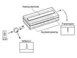
도 2는 본 발명의 바람직한 실시예에 따른 에포다이즈드 브래그 격자를 기반으로 하는 폴리머 가변 파장 필터의 구성도를 도시한 도면;
도 3은 본 발명의 바람직한 실시예에 따른 격자구조에서 여러가지 굴절률 분포에 대한 설계결과의 반사스펙트럼을 도시한 도면;
도 4는 본 발명의 바람직한 실시예에 따른 균일한 격자와 가우시안 격자의 조합으로 반사율, 3-dB 대역폭과 2-dB 대역폭을 계산한 결과를 도시한 도면;
도 5는 본 발명의 바람직한 실시예에 따른 유효굴절률 계산방법을 이용하여 높은 굴절률 차이가 나는 단일 모드 광도파로 설계 그래프를 도시한 도면;
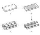
도 6은 본 발명의 바람직한 실시예에 따른 에포다이즈드 격자구조를 가지는 폴리머 광도파로 가변 파장 필터의 제작공정도를 도시한 도면;
도 7은 본 발명의 바람직한 실시예에 따른 에포다이즈드 격자를 제작하기 위해 산소 플라즈마 에칭 시 사용된 쉐도우 마스크 고정도를 도시한 도면;
도 8은 본 발명의 바람직한 실시예에 따른 에포다이즈드 격자구조를 가지는 파장 가변 필터의 투과 및 반사스펙트럼을 도시한 도면;
도 9는 본 발명의 바람직한 실시예에 따른 에포다이즈드 격자길이가 7mm인 필터의 파장가변 특성을 확인한 결과를 도시한 도면이다.BRIEF DESCRIPTION OF THE DRAWINGS FIG. 1 is a flowchart of a method for fabricating a polymer optical waveguide tunable filter based on an epodialized grating according to a preferred embodiment of the present invention; FIG.
FIG. 2 is a block diagram of a polymer variable wavelength filter based on an epodata Bragg grating according to a preferred embodiment of the present invention; FIG.
FIG. 3 illustrates a reflection spectrum of a design result for various refractive index distributions in a lattice structure according to a preferred embodiment of the present invention; FIG.
4 is a graph illustrating a result of calculating reflectance, a 3-dB bandwidth, and a 2-dB bandwidth using a combination of a uniform lattice and a Gaussian lattice according to a preferred embodiment of the present invention;
FIG. 5 illustrates a single mode optical waveguide design graph with a high refractive index difference using an effective refractive index calculation method according to a preferred embodiment of the present invention;
FIG. 6 is a view illustrating a manufacturing process of a polymer optical waveguide tunable filter having an epitaxial lattice structure according to a preferred embodiment of the present invention; FIG.
FIG. 7 is a diagram illustrating a shadow mask precision used in oxygen plasma etching to fabricate an epoxide grid according to a preferred embodiment of the present invention; FIG.
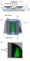
8 is a diagram showing transmission and reflection spectra of a wavelength tunable filter having an epitaxial lattice structure according to a preferred embodiment of the present invention;
FIG. 9 is a graph showing a result of checking wavelength tuning characteristics of a filter having an epiloaded grating length of 7 mm according to a preferred embodiment of the present invention.
필터 구조에 많이 사용되고 있는 Bragg grating의 반사율은 브래그 격자의 길이와 격자구조의 Index modulation에 의해 결정된다.
The reflectance of the Bragg grating, which is widely used in filter structures, is determined by the length of the Bragg grating and the index modulation of the grating structure.
반사율을 결정하는 두가지 요소에서 Index modulation이 작고 길이가 긴 격자를 이용하면 좁은 대역폭을 가지는 필터 제작이 가능하다. 하지만 브래그 격자의 modulation 값이 작은 구조에서 높은 반사율을 얻으려면 충분히 긴 길이의 격자가 필요하게 된다. 브래그 격자의 길이가 길어지면 격자를 균일하게 제작하기가 힘들며 파장가변을 할 경우 격자구조 전체에 동일한 열광학 효과를 여기 할 수 없기 때문에 대역폭이 넓어지는 문제점이 존재한다. 균일한 격자를 제작하기 위해서는 격자의 길이를 짧게 하는 것이 유리하지만 높은 반사율을 얻기 힘들다. 그러므로 짧은 격자길이에서 높은 반사율을 얻기 위해서는 격자에 의한 index modulation 값을 증가 시켜야 한다. 하지만 index modulation 값이 커지게 되면 대역폭이 넓어지게 된다. 이는 WDM 광통신시스템에서 인접한 채널의 파장신호로 인한 누화를 발생 시키는 원인이 된다.
In the two factors that determine the reflectance, it is possible to fabricate a filter with a narrow bandwidth by using a small index modulation and a long grating. However, in order to obtain a high reflectance in a structure having a small modulation value of the Bragg grating, a sufficiently long grating is required. If the length of the Bragg grating becomes long, it is difficult to fabricate the grating uniformly. If the wavelength tuning is performed, the same thermo-optic effect can not be excited in the entire grating structure. In order to produce a uniform grating, it is advantageous to shorten the grating length, but it is difficult to obtain a high reflectance. Therefore, in order to obtain a high reflectance in a short lattice length, the index modulation value by the lattice must be increased. However, the larger the index modulation value, the wider the bandwidth. This causes crosstalk due to the wavelength signal of the adjacent channel in the WDM optical communication system.
균일한 브래그 격자를 이용한 필터에 대한 연구가 많이 진행되고 있으며 소형의 가변파장필터를 구현하기 위해서는 격자의 길이가 짧아야 되고 짧은 격자에서 높은 반사율을 얻으려면 격자구조에서의 유효굴절률 차이가 커져야 된다. 이러한 문제점을 해결하기 위해 폴리머 광도파로에 대역폭을 줄일 수 있는 에포다이즈드 격자구조를 도입하였다.
Researches on a filter using a uniform Bragg grating have been conducted. In order to realize a small tunable filter, the length of the grating must be short. In order to obtain a high reflectance in a short grating, the effective refractive index difference in the grating structure must be large. To solve these problems, we introduced an ephodized lattice structure that can reduce the bandwidth of the polymer optical waveguide.
이하, 본 발명의 바람직한 실시예를 첨부된 도 1 내지 도 9에 의거하여 상세히 설명한다. 한편, 산소 플라즈마를 작동하는 관련 기술, 하부클래딩과 기판의 결합 관련 기술, 하부클래딩을 코팅하는 관련 기술 등 통상 본 발명에 적용되는 분야의 종사자들 및 그들이 관련분야의 종사자들 및 그들이 관련분야의 종사자들을 통해 통상적으로 알 수 있는 부분들의 도시 및 상세한 설명은 생략하고, 본 발명과 관련된 부분들을 중심으로 도시 및 설명 하였다.
Hereinafter, preferred embodiments of the present invention will be described in detail with reference to FIGS. 1 to 9. FIG. On the other hand, those skilled in the art to which the present invention applies, such as the related art for operating the oxygen plasma, the technology relating to bonding of the lower cladding and the substrate, and the related technology for coating the lower cladding, And the detailed description thereof will be omitted, and portions related to the present invention will be mainly shown and described.
도 1은 본 발명의 바람직한 실시예에 따른 에포다이즈드 격자를 기반으로 한 폴리머 광도파로 가변 파장 필터의 제작방법의 플로우차트를 도시한 도면이다.
BRIEF DESCRIPTION OF THE DRAWINGS FIG. 1 is a flowchart showing a method of manufacturing a polymer optical waveguide tunable filter based on an epodialized grating according to a preferred embodiment of the present invention. FIG.
도 1을 참조하면, 폴리머 광도파로 가변 파장 필터의 제작방법은 클래딩 형성 단계, 브래그 격자 형성단계, 고정 단계, 에포다이즈드 격자 형성단계로 구성된다.
Referring to FIG. 1, a method for fabricating a polymer optical waveguide tunable filter includes a cladding formation step, a Bragg grating formation step, a fixing step, and an epitaxial grating formation step.
이와 같은 폴리머 광도파로 가변 파장 필터의 제작방법은 코팅된 하부클래딩(12)을 기판(11) 위에 형성하는 클래딩 형성 단계를 갖는다. 다음으로 하부클래딩(12)에 레이저 간섭계를 이용하여 브래그 격자를 새기는 브래그 격자 형성단계를 가지며 브래그 격자 상에 쉐도우 마스크(13)(shadow mask)를 격자영역 위에 조정하는 고정 단계를 갖는다. 고정 단계 후, 산소 플라즈마(14)로부터 노출된 격자영역의 중심에서 양측으로 가면서 에칭된 격자의 깊이가 서서히 감소하게 되어 격자를 형성하는 에포다이즈드 격자 형성단계를 가짐으로써 산소 플라즈마(14)로 노출된 격자에 의해 에포다이즈드 격자를 형성하며 에칭 깊이가 방향에 따라 서서히 변화하여 에포다이즈드 격자를 기반으로 한 폴리머 광도파로 가변 파장 필터를 제작하도록 한다.
The method of fabricating such a polymer optical waveguide tunable filter has a cladding formation step of forming a coated
클래딩 형성 단계에서 코팅은 폴리머를 스핀 코팅하여 하부클래딩(12)을 형성하도록 한다. 또한, 에포다이즈드 격자 형성 단계 전, 한개소 이상의 스페이서(15)를 사용하여 산소 플라즈마(14)가 표면으로 침투해 들어가는 것을 막도록 스페이서(15) 구비단계를 더 포함하도록 한다.
In the cladding-forming step, the coating is spin-coated with the polymer to form the
도 2는 본 발명의 바람직한 실시예에 따른 에포다이즈드 브래그 격자를 기반으로 하는 폴리머 가변 파장 필터의 구성도를 도시한 도면이다.
FIG. 2 is a block diagram of a polymer variable wavelength filter based on an epodata Bragg grating according to a preferred embodiment of the present invention. Referring to FIG.
도 2를 참조하면, 높은 반사율을 가지면서 좁은 대역폭을 갖는 소형의 필터를 구현하기 위해서 에포다이즈드 격자 구조를 가지는 필터를 제안한다. 격자구조는 코어 클래딩층 사이에 형성되어 있으며 격자구조의 깊이는 광파의 진행방향에 따라 서서히 변화하고 격자의 반사율도 서서히 변화하게 된다. 브래그 격자의 반사파장을 가변화하기 위해 금속 히터가 격자구조 패턴영역의 위에 형성되어 있다.
Referring to FIG. 2, a filter having a pseudo-grating structure is proposed in order to realize a small-sized filter having a high reflectance and a narrow bandwidth. The lattice structure is formed between the core cladding layers, and the depth of the lattice structure gradually changes according to the traveling direction of the light wave, and the reflectance of the lattice gradually changes. In order to vary the reflection wavelength of the Bragg grating, a metal heater is formed on the grating pattern area.
도 3은 본 발명의 바람직한 실시예에 따른 격자구조에서 여러가지 굴절률 분포에 대한 설계결과의 반사스펙트럼을 도시한 도면이다.
FIG. 3 is a diagram showing reflection spectra of design results for various refractive index distributions in a lattice structure according to a preferred embodiment of the present invention.
도 3을 참조하면, 에포다이즈드 브래그 격자를 설계하기 위해 광파의 진행방향에 따라 격자구조의 유효굴절률 계산을 통해 transmission matrix method를 이용하였다.
Referring to FIG. 3, a transmission matrix method is used to calculate an effective refractive index of a grating structure in accordance with the traveling direction of a light wave in order to design an epodata Bragg grating.
균일한 격자인 경우 maximum index modulation 값을
For a uniform grid, the maximum index modulation value
도 3(b)와 같이 가우시안 에포다이즈드 격자 설계 결과를 보여주고 있는데 20-dB 대역폭은 균일한 격자에 비해 많이 줄었지만 95%이상의 반사율을 얻으려면 격자의 길이가 10nm 이상이 되어야 한다. 격자의 길이를 줄이기 위해 구조 조정된 격자구조를 도 3(c)에서 보여주고 있다.
As shown in FIG. 3 (b), the results of the pseudo-grating design are shown in Gaussian. The 20-dB bandwidth is much smaller than the uniform grating, but the grating length must be 10 nm or more to obtain a reflectance of 95% or more. The structured grating structure to reduce the length of the grating is shown in Figure 3 (c).
도 4는 본 발명의 바람직한 실시예에 따른 균일한 격자와 가우시안 격자의 조합으로 반사율, 3-dB 대역폭과 20-dB 대역폭을 계산한 결과를 도시한 도면이다.
FIG. 4 is a graph showing the reflectance, 3-dB bandwidth, and 20-dB bandwidth calculated by a combination of a uniform grating and a Gaussian grating according to a preferred embodiment of the present invention.
도 4를 참조하면, 제안한 구조는 균일한 격자길이

Referring to FIG. 4, the proposed structure has a uniform grating length
짧은 격자에서 적합한 반사율과 대역폭을 얻기 위해 균일한 격자길이

In order to obtain adequate reflectivity and bandwidth in a short lattice, a uniform lattice length
주어진 격자길이에서


At a given lattice length
굴절률 차이가 큰 광도파로 제작하기 위해 코어와 클래딩의 물질은 각각 1.455와 1.430으로 하였다. 코어와 클래딩 물질의 굴절률 차이가 크면 격자구조가 작은 깊이에서도 높은 굴절률 차이가 나타나 높은 반사율을 얻을 수 있다.
The materials of core and cladding were 1.455 and 1.430, respectively, to fabricate optical waveguide with large refractive index difference. When the refractive index difference between the core and the cladding material is large, a high refractive index difference can be obtained because of a high refractive index difference even at a small depth of the lattice structure.
도 5는 본 발명의 바람직한 실시예에 따른 유효굴절률 계산방법을 이용하여 높은 굴절률 차이가 나는 단일 모드 광도파로 설계 그래프를 도시한 도면이다.
FIG. 5 is a diagram illustrating a single mode optical waveguide design graph having a high refractive index difference using the effective refractive index calculating method according to a preferred embodiment of the present invention.
도 5를 참조하면, 단일모드 광도파로를 제작하기 위해 유효굴절률법을 이용하여 계산한 결과를 도 5(a)에서 보여주고 있으며, 코의 두께가 2.5㎛일 때 유효굴절률이 1.44475이고 lateral 코어의 두께가 1.3㎛일 때 유효굴절률이 1.43775라는 것을 알 수 있다.
FIG. 5 (a) shows the result of calculation using the effective refractive index method to fabricate a single-mode optical waveguide. When the thickness of the nose is 2.5 μm, the effective refractive index is 1.44475, It can be seen that the effective refractive index is 1.43775 when the thickness is 1.3 mu m.
위에서 계산한 두 유효굴절률을 이용하여 광도파로의 두께에 따른 유효굴절률 값을 도 5(b)에서 보여주고 있으며 설계한 광도파로는 단일모드임을 알 수 있다. 또한, 격자구조의 깊이가 200nm일 때 격자구조로 인한 굴절률 변화는이고 짧은 격자에서도 높은 반사율을 얻을 수 있다.
The effective refractive index according to the thickness of the optical waveguide is shown in FIG. 5 (b) using the two effective refractive indexes calculated above, and it can be seen that the designed optical waveguide is in a single mode. Also, when the depth of the lattice structure is 200 nm, the refractive index change due to the lattice structure is And a high reflectance can be obtained even in a short lattice.
도 6은 본 발명의 바람직한 실시예에 따른 에포다이즈드 격자구조를 가지는 폴리머 광도파로 가변 파장 필터의 제작공정도를 도시한 도면이다.
FIG. 6 is a view showing a manufacturing process of a polymer optical waveguide tunable filter having an epicatequent lattice structure according to a preferred embodiment of the present invention.
도 6을 참조하면, 에포다이즈드 격자구조를 가지는 가변 파장 필터를 제작하기 위해 굴절률차이가 0.025 인 켐옵틱스사의 두 가지 ZPU 폴리머를 사용하였다. 광도파로는 코어의 크기가 4㎛ x 2.7㎛ 이고 평면도파로의 두께는 1.3㎛ 인 립형태로 제작되었다. 먼저 굴절률이 1.430 인 폴리머를 스핀 코팅하여 하부 클래딩을 실리콘 기판(11)위에 형성하였다. 그 다음 하부 클래딩에 레이저 간섭계를 이용하여 주기가 546.8 nm 인 TSMR photoresist 브래그 격자를 새겨놓았다. 에포다이즈드 격자를 제작하기 위해 쉐도우 마스크(13)를 격자영역 위에 고정해 놓고 산소 플라즈마(14) 에칭을 통해 격자패턴이 하부 클래딩에 새겨지도록 하였다.
Referring to FIG. 6, two ZPU polymers of Chem Optics Inc. having a refractive index difference of 0.025 were used to fabricate a tunable wavelength filter having an epodized lattice structure. The optical waveguide was fabricated in the form of a lip having a core size of 4 탆 x 2.7 탆 and a planar waveguide thickness of 1.3 탆. First, a polymer having a refractive index of 1.430 was spin-coated to form a lower cladding on the
도 7은 본 발명의 바람직한 실시예에 따른 에포다이즈드 격자를 제작하기 위해 산소 플라즈마 에칭 시 사용된 쉐도우 마스크 고정도를 도시한 도면이다.
FIG. 7 is a diagram showing a shadow mask high-accuracy used in oxygen plasma etching to fabricate an epoxide grid according to a preferred embodiment of the present invention.
도 7을 참조하면, 쉐도우 마스크(13)를 이용한 산소 플라즈마(14) 에칭공정을 진행하였다. 높이를 조절할 수 있는 스페이서(15) 를 이용하여 샘플위에 쉐도우 마스크(13)를 고정해 놓았고 또 이 스페이서(15)는 측면으로 흘러 들어가는 활성 기체를 막아주는 작용을 하기도 한다. 마스크가 덮여진 영역의 내부로 들어가면서 플라즈마 양이 점점 줄어들고 이로 인해 격자구조가 에칭되는 깊이가 점차적으로 줄어 들게 된다. 중심부에서 양쪽방향으로 가면서 격자의 깊이가 서서히 줄어드는 구조를 가지게 되고 이렇게 형성된 에포다이즈드 격자를 이용하여 대역폭이 좁은 반사스펙트럼을 얻을 수 있다.
Referring to FIG. 7, the
도 7(a)와 도 7(b)에서 보여주고 있듯이 쉐도우 마스크(13)는 샘플의 위에 놓여 있다. 에포다이즈드 격자 제작과정에서 4개의 스페이서(15)가 사용되는데 에칭과정에서 산소 플라즈마(14)가 샘플표면으로 침투해 들어가는 것을 막아주는 작용을 한다. 플라즈마에 노출된 격자영역의 중심에서 엣지쪽으로 가면서 에칭된 격자의 깊이가 서서히 감소하게 되고 에포다이즈드 격자가 도 7(c)에서처럼 하부 클래딩에 새겨지게 된다.
As shown in Figs. 7 (a) and 7 (b), the
에포다이즈드격자 위에 굴절률이 1.455 이고 두께가 2.7㎛ 인 폴리머 코어층을 스핀코팅을 하였고 포토리소그래피와 드라이 에칭공정을 이용하여 립 형태의 광도파로를 제작하였다. 굴절률이 1.430 인 폴리머를 9㎛ 두께로 스핀코팅하여 상부 클래딩을 형성하였다. 그 위에 파장 가변을 하기 위해 마이크로 히터를 제작하였다.
A polymer core layer having a refractive index of 1.455 and a thickness of 2.7 탆 was spin-coated on the pseudodized lattice, and a lip type optical waveguide was formed by photolithography and dry etching. A polymer having a refractive index of 1.430 was spin-coated to a thickness of 9 mu m to form an upper cladding. A micro heater was fabricated to change the wavelength.
도 8은 본 발명의 바람직한 실시예에 따른 에포다이즈드 격자구조를 가지는 파장 가변 필터의 투과 및 반사스펙트럼을 도시한 도면이다.
FIG. 8 is a diagram illustrating transmission and reflection spectra of a wavelength tunable filter having an epitaxial lattice structure according to a preferred embodiment of the present invention.
제작된 가변파장 필터의 특성을 확인하기 위해 중심 파장이 1550 nm 이며 대역폭이 60 nm 인 SLED 를 광원으로 사용하였으며 입력광의 편광은 TE 모드로 유지하였다. 에포다이즈드 격자에 의해 반사된 신호는 circulator 를 통해 optical spectrum analyzer(OSA) 에서 측정되었다. 투과스펙트럼과 반사스펙트럼은 도 7에서 보여주고 있으며 브래그 반사픽은 1576.7 nm 에서 나타났다. 격자 길이가 7 mm 인 경우 95% 정도의 반사율을 가지고 3-dB 와 20-dB bandwidth 는 각각 0.36 nm 와 0.72 nm 임을 확인하였다. Flat-top passband 는 0.5-dB 대역폭으로 정의하고 0.18 nm 였다.
In order to verify the characteristics of the fabricated variable wavelength filter, the SLED with a center wavelength of 1550 nm and a bandwidth of 60 nm was used as the light source and the polarization of the input light was maintained in the TE mode. The signal reflected by the pseudo-grating was measured by an optical spectrum analyzer (OSA) through a circulator. The transmission spectrum and the reflection spectrum are shown in Fig. 7, and the Bragg reflection pic was shown at 1576.7 nm. It was confirmed that the 3-dB and 20-dB bandwidths were 95% and 0.72 nm, respectively, when the grating length was 7 mm. The flat-top passband was defined as a 0.5-dB bandwidth and was 0.18 nm.
도 9는 본 발명의 바람직한 실시예에 따른 에포다이즈드 격자길이가 7mm인 필터의 파장가변 특성을 확인한 결과를 도시한 도면이다.
FIG. 9 is a graph showing a result of checking wavelength tuning characteristics of a filter having an epiloaded grating length of 7 mm according to a preferred embodiment of the present invention.
열광학효과를 이용한 가변 파장필터의 가변특성을 확인하기 위해 얇은 필름 히터에 파워 supply 를 연결해 주었다. 히터에 인가한 파워가 증가하면서 변화하는 반사스펙트럼을 측정한 결과를 도 9에서 보여주고 있다. 509 mW 의 thermal power 를 인가하였을 때 14 nm 이상 파장 가변이 가능함을 알 수 있다. 파장 가변과정에서 반사스펙트럼의 모양은 유지가 되고 있지만 10 nm 이상으로 가변되었을 때 스펙트럼이 조금 넓어진 것을 볼 수 있다. 에포다이즈드 격자 구조가 광의 진행방항에 대해 균일하게 제작되지 않았기 때문에 thermal power 가 증가할수록 격자 구조에 의한 굴절률 변화가 달라져 반사스펙트럼의 대역폭이 점점 증가하는 것을 알 수 있다. 히터의 온도가 높음으로 인해 굴절률변화가 크게 되면 전파모드의 파워는 떨어지게 되고 격자의 반사율도 떨어지게 된다. 필터의 파장가변 특성은 마이크로 히터의 열에 비례해 선형적으로 나타나고 있고 파장가변 효율은 27 nm/W 이라는 것을 도 9(b)에서 보여주고 있다.
A thin film heater was connected to the power supply to check the variable characteristics of the variable wavelength filter using the thermo - optic effect. The results of measuring the varying reflection spectrum while increasing the power applied to the heater are shown in Fig. When the thermal power of 509 mW is applied, it can be seen that the wavelength is more than 14 nm. The shape of the reflection spectrum is maintained in the wavelength tuning process, but the spectrum is slightly widened when it is tuned to 10 nm or more. Since the pseudo-grating structure is not uniformly fabricated with respect to the propagation direction of the light, it can be seen that the bandwidth of the reflection spectrum is gradually increased due to the change of the refractive index due to the lattice structure as the thermal power is increased. When the temperature of the heater is high, the change of the refractive index becomes large, the power of the propagation mode decreases and the reflectance of the grating decreases. FIG. 9 (b) shows that the wavelength tunable characteristic of the filter is linearly proportional to the heat of the micro heater and the wavelength tuning efficiency is 27 nm / W.
상술한 바와 같은, 본 발명의 바람직한 실시예에 따른 에포다이즈드 격자를 기반으로 한 폴리머 광도파로 가변 파장 필터의 제작방법을 상기한 설명 및 도면에 따라 도시 하였지만, 이는 예를 들어 설명한 것에 불과하며 본 발명의 기술적 사상을 벗어나지 않는 범위 내에서 다양한 변화 및 변경 가능하다는 것을 이 분야의 통상적인 기술자들은 잘 이해할 수 있을 것이다.
Although the method of fabricating the polymer optical waveguide tunable filter based on the epodized grid according to the preferred embodiment of the present invention as described above has been described according to the above description and drawings, It will be understood by those skilled in the art that various changes and modifications may be made without departing from the spirit of the invention.
11 : 기판
12 : 하부클래딩
13 : 쉐도우 마스크
14 : 산소 플라즈마
15 : 스페이서11: substrate
12: Lower cladding
13: Shadow mask
14: oxygen plasma
15: Spacer
Claims (3)
Translated fromKorean상기 하부클래딩에 레이저 간섭계를 이용하여 브래그 격자를 새기는 브래그 격자 형성단계; 와
상기 브래그 격자 상에 산소 플라즈마가 표면으로 침투해 들어가는 것을 막는 한개소 이상의 스페이서를 사용하여 쉐도우 마스크를 격자영역 위에 고정하는 고정 단계; 및
상기 고정 단계 후, 산소 플라즈마로부터 노출된 격자영역의 중심에서 양측으로 격자를 형성하는 에포다이즈드 격자 형성단계를 포함하고
상기 형성단계는 상기 산소 플라즈마로 노출된 격자에 의해 에포다이즈드 격자를 형성하되 상기 고정 단계의 상기 쉐도우 마스크에 의해 상기 산소 플라즈마 양이 감소함으로써 에칭의 깊이가 서서히 변화하는 것을 특징으로 하는 에포다이즈드 격자를 기반으로 한 폴리머 광도파로 가변 파장 필터의 제작방법.
A cladding formation step of forming a lower cladding on the substrate; Wow
Forming a Bragg grating on the lower cladding using a laser interferometer to grasp the Bragg grating; Wow
A fixing step of fixing the shadow mask on the grating area using at least one spacer on the Bragg grating to prevent penetration of oxygen plasma into the surface; And
And forming an etch lattice on both sides of the center of the lattice region exposed from the oxygen plasma after the fixing step,
Wherein the forming step forms an epitaxial lattice by the lattice exposed by the oxygen plasma, wherein the depth of the etching is gradually changed by decreasing the oxygen plasma amount by the shadow mask in the fixing step. A Fabrication Method of Polymer Optical Waveguide Tunable Filters Based on Izd Grid.
상기 에포다이즈드 격자 형성시, 상기 스페이서의 두께를 조절하여 상기 에포다이즈드 격자의 형상을 조절하는 단계를 더 포함하는 폴리머 광도파로 가변 파장 필터의 제작방법.The method according to claim 1,
Further comprising the step of adjusting the thickness of the spacer to adjust the shape of the epilayered grating when forming the epilayered grating. ≪ RTI ID = 0.0 > 8. < / RTI >
Priority Applications (1)
| Application Number | Priority Date | Filing Date | Title |
|---|---|---|---|
| KR1020150128746AKR101759727B1 (en) | 2015-09-11 | 2015-09-11 | Apodized Gratings for Polymeric Waveguide Tunable Wavelength Filters in the manufacturing method |
Applications Claiming Priority (1)
| Application Number | Priority Date | Filing Date | Title |
|---|---|---|---|
| KR1020150128746AKR101759727B1 (en) | 2015-09-11 | 2015-09-11 | Apodized Gratings for Polymeric Waveguide Tunable Wavelength Filters in the manufacturing method |
Publications (2)
| Publication Number | Publication Date |
|---|---|
| KR20170031357A KR20170031357A (en) | 2017-03-21 |
| KR101759727B1true KR101759727B1 (en) | 2017-07-20 |
Family
ID=58502411
Family Applications (1)
| Application Number | Title | Priority Date | Filing Date |
|---|---|---|---|
| KR1020150128746AExpired - Fee RelatedKR101759727B1 (en) | 2015-09-11 | 2015-09-11 | Apodized Gratings for Polymeric Waveguide Tunable Wavelength Filters in the manufacturing method |
Country Status (1)
| Country | Link |
|---|---|
| KR (1) | KR101759727B1 (en) |
Families Citing this family (19)
| Publication number | Priority date | Publication date | Assignee | Title |
|---|---|---|---|---|
| US11726332B2 (en) | 2009-04-27 | 2023-08-15 | Digilens Inc. | Diffractive projection apparatus |
| WO2016020630A2 (en) | 2014-08-08 | 2016-02-11 | Milan Momcilo Popovich | Waveguide laser illuminator incorporating a despeckler |
| US9933684B2 (en) | 2012-11-16 | 2018-04-03 | Rockwell Collins, Inc. | Transparent waveguide display providing upper and lower fields of view having a specific light output aperture configuration |
| WO2016042283A1 (en) | 2014-09-19 | 2016-03-24 | Milan Momcilo Popovich | Method and apparatus for generating input images for holographic waveguide displays |
| WO2016113534A1 (en) | 2015-01-12 | 2016-07-21 | Milan Momcilo Popovich | Environmentally isolated waveguide display |
| US9632226B2 (en) | 2015-02-12 | 2017-04-25 | Digilens Inc. | Waveguide grating device |
| CN113759555B (en) | 2015-10-05 | 2024-09-20 | 迪吉伦斯公司 | Waveguide Display |
| WO2018102834A2 (en) | 2016-12-02 | 2018-06-07 | Digilens, Inc. | Waveguide device with uniform output illumination |
| US10545346B2 (en) | 2017-01-05 | 2020-01-28 | Digilens Inc. | Wearable heads up displays |
| EP3710894B1 (en) | 2018-01-08 | 2025-07-30 | Digilens Inc. | Methods for fabricating optical waveguides |
| US10732569B2 (en) | 2018-01-08 | 2020-08-04 | Digilens Inc. | Systems and methods for high-throughput recording of holographic gratings in waveguide cells |
| US20200225471A1 (en) | 2019-01-14 | 2020-07-16 | Digilens Inc. | Holographic Waveguide Display with Light Control Layer |
| US20200247017A1 (en) | 2019-02-05 | 2020-08-06 | Digilens Inc. | Methods for Compensating for Optical Surface Nonuniformity |
| KR102866596B1 (en) | 2019-02-15 | 2025-09-29 | 디지렌즈 인코포레이티드. | Method and device for providing a holographic waveguide display using an integral grating |
| US20220283377A1 (en) | 2019-02-15 | 2022-09-08 | Digilens Inc. | Wide Angle Waveguide Display |
| EP3980825A4 (en) | 2019-06-07 | 2023-05-03 | Digilens Inc. | WAVEGUIDES WITH TRANSMITTING AND REFLECTING GRIDS AND RELATED MANUFACTURING PROCESSES |
| KR102775783B1 (en) | 2019-08-29 | 2025-02-28 | 디지렌즈 인코포레이티드. | Vacuum grid and method for manufacturing the same |
| WO2022150841A1 (en) | 2021-01-07 | 2022-07-14 | Digilens Inc. | Grating structures for color waveguides |
| US12158612B2 (en) | 2021-03-05 | 2024-12-03 | Digilens Inc. | Evacuated periodic structures and methods of manufacturing |
Citations (2)
| Publication number | Priority date | Publication date | Assignee | Title |
|---|---|---|---|---|
| JP2012054367A (en)* | 2010-08-31 | 2012-03-15 | Nippon Telegr & Teleph Corp <Ntt> | Semiconductor element, and method of manufacturing the same |
| JP2014516479A (en) | 2011-04-25 | 2014-07-10 | オーエフエス ファイテル,エルエルシー | Raman distributed feedback fiber laser and high power laser system using the same |
- 2015
- 2015-09-11KRKR1020150128746Apatent/KR101759727B1/ennot_activeExpired - Fee Related
Patent Citations (2)
| Publication number | Priority date | Publication date | Assignee | Title |
|---|---|---|---|---|
| JP2012054367A (en)* | 2010-08-31 | 2012-03-15 | Nippon Telegr & Teleph Corp <Ntt> | Semiconductor element, and method of manufacturing the same |
| JP2014516479A (en) | 2011-04-25 | 2014-07-10 | オーエフエス ファイテル,エルエルシー | Raman distributed feedback fiber laser and high power laser system using the same |
Also Published As
| Publication number | Publication date |
|---|---|
| KR20170031357A (en) | 2017-03-21 |
Similar Documents
| Publication | Publication Date | Title |
|---|---|---|
| KR101759727B1 (en) | Apodized Gratings for Polymeric Waveguide Tunable Wavelength Filters in the manufacturing method | |
| Wiesmann et al. | Apodized surface-corrugated gratings with varying duty cycles | |
| EP0880036B1 (en) | Method for altering the temperature dependence of optical waveguide devices | |
| KR101443997B1 (en) | An optical filter or multiplexer/demultiplexer | |
| KR100299662B1 (en) | Thermo-optical variable wavelength filter manufacturing method | |
| US7634165B2 (en) | Monolithic tunable lasers and reflectors | |
| JP5357214B2 (en) | Optical integrated circuit | |
| US20050141811A1 (en) | Tunable filter and the method for making the same | |
| US20020094166A1 (en) | Segmented waveguide flattening the passband of a phasar | |
| KR100943561B1 (en) | Wavelength filter manufacturing method | |
| US9927676B2 (en) | Optical device with integrated reflector(s) comprising a loop reflector integrating a mach-zehnder interferometer | |
| JP5998651B2 (en) | Optical transmitter | |
| US8676023B2 (en) | Method of fabrication for an asymmetric Bragg coupler-based polymeric wavelength filter with single-grating waveguide | |
| KR102522956B1 (en) | Polymeric waveguide Bragg reflecting tunable wavelength filters | |
| KR101782593B1 (en) | Polymer waveguide tunable wavelength filters consisting of mode sorting waveguide and tilted Bragg grating | |
| Veerasubramanian et al. | Design and demonstration of apodized comb filters on SOI | |
| WO2002079863A2 (en) | Optoelectronic filters | |
| Chen et al. | Athermal narrow-band filters based on side-modulated bragg gratings | |
| Park et al. | Optimization of tilted Bragg grating tunable filters based on polymeric optical waveguides | |
| AU765250B2 (en) | Optical components | |
| KR101704786B1 (en) | Polymeric waveguide devices with high reflectivity Bragg gratings | |
| KR101636940B1 (en) | Polymeric Bragg reflection tunable wavelength filters and its Manufacturing method | |
| Kokubun | Waveguide filters and related technologies: issues and solutions for practical use in transmission systems | |
| US20030198438A1 (en) | Tunable add/drop multiplexer | |
| Hammood et al. | Silicon photonic bragg grating devices |
Legal Events
| Date | Code | Title | Description |
|---|---|---|---|
| A201 | Request for examination | ||
| PA0109 | Patent application | St.27 status event code:A-0-1-A10-A12-nap-PA0109 | |
| PA0201 | Request for examination | St.27 status event code:A-1-2-D10-D11-exm-PA0201 | |
| R18-X000 | Changes to party contact information recorded | St.27 status event code:A-3-3-R10-R18-oth-X000 | |
| D13-X000 | Search requested | St.27 status event code:A-1-2-D10-D13-srh-X000 | |
| D14-X000 | Search report completed | St.27 status event code:A-1-2-D10-D14-srh-X000 | |
| E902 | Notification of reason for refusal | ||
| PE0902 | Notice of grounds for rejection | St.27 status event code:A-1-2-D10-D21-exm-PE0902 | |
| E13-X000 | Pre-grant limitation requested | St.27 status event code:A-2-3-E10-E13-lim-X000 | |
| P11-X000 | Amendment of application requested | St.27 status event code:A-2-2-P10-P11-nap-X000 | |
| P13-X000 | Application amended | St.27 status event code:A-2-2-P10-P13-nap-X000 | |
| E90F | Notification of reason for final refusal | ||
| PE0902 | Notice of grounds for rejection | St.27 status event code:A-1-2-D10-D21-exm-PE0902 | |
| R18-X000 | Changes to party contact information recorded | St.27 status event code:A-3-3-R10-R18-oth-X000 | |
| R18-X000 | Changes to party contact information recorded | St.27 status event code:A-3-3-R10-R18-oth-X000 | |
| P11-X000 | Amendment of application requested | St.27 status event code:A-2-2-P10-P11-nap-X000 | |
| P13-X000 | Application amended | St.27 status event code:A-2-2-P10-P13-nap-X000 | |
| PG1501 | Laying open of application | St.27 status event code:A-1-1-Q10-Q12-nap-PG1501 | |
| PE0701 | Decision of registration | St.27 status event code:A-1-2-D10-D22-exm-PE0701 | |
| PR0701 | Registration of establishment | St.27 status event code:A-2-4-F10-F11-exm-PR0701 | |
| PR1002 | Payment of registration fee | Fee payment year number:1 St.27 status event code:A-2-2-U10-U11-oth-PR1002 | |
| PG1601 | Publication of registration | St.27 status event code:A-4-4-Q10-Q13-nap-PG1601 | |
| P22-X000 | Classification modified | St.27 status event code:A-4-4-P10-P22-nap-X000 | |
| PR1001 | Payment of annual fee | Fee payment year number:4 St.27 status event code:A-4-4-U10-U11-oth-PR1001 | |
| PR1001 | Payment of annual fee | Fee payment year number:5 St.27 status event code:A-4-4-U10-U11-oth-PR1001 | |
| PC1903 | Unpaid annual fee | Not in force date:20220714 Payment event data comment text:Termination Category : DEFAULT_OF_REGISTRATION_FEE St.27 status event code:A-4-4-U10-U13-oth-PC1903 | |
| PC1903 | Unpaid annual fee | Ip right cessation event data comment text:Termination Category : DEFAULT_OF_REGISTRATION_FEE Not in force date:20220714 St.27 status event code:N-4-6-H10-H13-oth-PC1903 | |
| PN2301 | Change of applicant | St.27 status event code:A-5-5-R10-R11-asn-PN2301 St.27 status event code:A-5-5-R10-R13-asn-PN2301 | |
| R18-X000 | Changes to party contact information recorded | St.27 status event code:A-5-5-R10-R18-oth-X000 | |
| PN2301 | Change of applicant | St.27 status event code:A-5-5-R10-R11-asn-PN2301 St.27 status event code:A-5-5-R10-R13-asn-PN2301 | |
| R18-X000 | Changes to party contact information recorded | St.27 status event code:A-5-5-R10-R18-oth-X000 | |
| P22-X000 | Classification modified | St.27 status event code:A-4-4-P10-P22-nap-X000 |