KR101751902B1 - Display device and semiconductor device - Google Patents
Display device and semiconductor deviceDownload PDFInfo
- Publication number
- KR101751902B1 KR101751902B1KR1020127013230AKR20127013230AKR101751902B1KR 101751902 B1KR101751902 B1KR 101751902B1KR 1020127013230 AKR1020127013230 AKR 1020127013230AKR 20127013230 AKR20127013230 AKR 20127013230AKR 101751902 B1KR101751902 B1KR 101751902B1
- Authority
- KR
- South Korea
- Prior art keywords
- photosensor
- detected
- display panel
- pixels
- light
- Prior art date
- Legal status (The legal status is an assumption and is not a legal conclusion. Google has not performed a legal analysis and makes no representation as to the accuracy of the status listed.)
- Expired - Fee Related
Links
Images


Classifications
- G—PHYSICS
- G06—COMPUTING OR CALCULATING; COUNTING
- G06F—ELECTRIC DIGITAL DATA PROCESSING
- G06F3/00—Input arrangements for transferring data to be processed into a form capable of being handled by the computer; Output arrangements for transferring data from processing unit to output unit, e.g. interface arrangements
- G06F3/01—Input arrangements or combined input and output arrangements for interaction between user and computer
- G06F3/03—Arrangements for converting the position or the displacement of a member into a coded form
- G06F3/041—Digitisers, e.g. for touch screens or touch pads, characterised by the transducing means
- G06F3/0412—Digitisers structurally integrated in a display
- G—PHYSICS
- G02—OPTICS
- G02F—OPTICAL DEVICES OR ARRANGEMENTS FOR THE CONTROL OF LIGHT BY MODIFICATION OF THE OPTICAL PROPERTIES OF THE MEDIA OF THE ELEMENTS INVOLVED THEREIN; NON-LINEAR OPTICS; FREQUENCY-CHANGING OF LIGHT; OPTICAL LOGIC ELEMENTS; OPTICAL ANALOGUE/DIGITAL CONVERTERS
- G02F1/00—Devices or arrangements for the control of the intensity, colour, phase, polarisation or direction of light arriving from an independent light source, e.g. switching, gating or modulating; Non-linear optics
- G02F1/01—Devices or arrangements for the control of the intensity, colour, phase, polarisation or direction of light arriving from an independent light source, e.g. switching, gating or modulating; Non-linear optics for the control of the intensity, phase, polarisation or colour
- G02F1/13—Devices or arrangements for the control of the intensity, colour, phase, polarisation or direction of light arriving from an independent light source, e.g. switching, gating or modulating; Non-linear optics for the control of the intensity, phase, polarisation or colour based on liquid crystals, e.g. single liquid crystal display cells
- G02F1/133—Constructional arrangements; Operation of liquid crystal cells; Circuit arrangements
- G02F1/1333—Constructional arrangements; Manufacturing methods
- G02F1/13338—Input devices, e.g. touch panels
- G—PHYSICS
- G06—COMPUTING OR CALCULATING; COUNTING
- G06F—ELECTRIC DIGITAL DATA PROCESSING
- G06F3/00—Input arrangements for transferring data to be processed into a form capable of being handled by the computer; Output arrangements for transferring data from processing unit to output unit, e.g. interface arrangements
- G06F3/01—Input arrangements or combined input and output arrangements for interaction between user and computer
- G06F3/03—Arrangements for converting the position or the displacement of a member into a coded form
- G06F3/0304—Detection arrangements using opto-electronic means
- G—PHYSICS
- G06—COMPUTING OR CALCULATING; COUNTING
- G06F—ELECTRIC DIGITAL DATA PROCESSING
- G06F3/00—Input arrangements for transferring data to be processed into a form capable of being handled by the computer; Output arrangements for transferring data from processing unit to output unit, e.g. interface arrangements
- G06F3/01—Input arrangements or combined input and output arrangements for interaction between user and computer
- G06F3/03—Arrangements for converting the position or the displacement of a member into a coded form
- G06F3/041—Digitisers, e.g. for touch screens or touch pads, characterised by the transducing means
- G06F3/042—Digitisers, e.g. for touch screens or touch pads, characterised by the transducing means by opto-electronic means
- G—PHYSICS
- G09—EDUCATION; CRYPTOGRAPHY; DISPLAY; ADVERTISING; SEALS
- G09G—ARRANGEMENTS OR CIRCUITS FOR CONTROL OF INDICATING DEVICES USING STATIC MEANS TO PRESENT VARIABLE INFORMATION
- G09G3/00—Control arrangements or circuits, of interest only in connection with visual indicators other than cathode-ray tubes
- G09G3/20—Control arrangements or circuits, of interest only in connection with visual indicators other than cathode-ray tubes for presentation of an assembly of a number of characters, e.g. a page, by composing the assembly by combination of individual elements arranged in a matrix no fixed position being assigned to or needed to be assigned to the individual characters or partial characters
- G09G3/22—Control arrangements or circuits, of interest only in connection with visual indicators other than cathode-ray tubes for presentation of an assembly of a number of characters, e.g. a page, by composing the assembly by combination of individual elements arranged in a matrix no fixed position being assigned to or needed to be assigned to the individual characters or partial characters using controlled light sources
- G09G3/30—Control arrangements or circuits, of interest only in connection with visual indicators other than cathode-ray tubes for presentation of an assembly of a number of characters, e.g. a page, by composing the assembly by combination of individual elements arranged in a matrix no fixed position being assigned to or needed to be assigned to the individual characters or partial characters using controlled light sources using electroluminescent panels
- G09G3/32—Control arrangements or circuits, of interest only in connection with visual indicators other than cathode-ray tubes for presentation of an assembly of a number of characters, e.g. a page, by composing the assembly by combination of individual elements arranged in a matrix no fixed position being assigned to or needed to be assigned to the individual characters or partial characters using controlled light sources using electroluminescent panels semiconductive, e.g. using light-emitting diodes [LED]
- G—PHYSICS
- G09—EDUCATION; CRYPTOGRAPHY; DISPLAY; ADVERTISING; SEALS
- G09G—ARRANGEMENTS OR CIRCUITS FOR CONTROL OF INDICATING DEVICES USING STATIC MEANS TO PRESENT VARIABLE INFORMATION
- G09G3/00—Control arrangements or circuits, of interest only in connection with visual indicators other than cathode-ray tubes
- G09G3/20—Control arrangements or circuits, of interest only in connection with visual indicators other than cathode-ray tubes for presentation of an assembly of a number of characters, e.g. a page, by composing the assembly by combination of individual elements arranged in a matrix no fixed position being assigned to or needed to be assigned to the individual characters or partial characters
- G09G3/34—Control arrangements or circuits, of interest only in connection with visual indicators other than cathode-ray tubes for presentation of an assembly of a number of characters, e.g. a page, by composing the assembly by combination of individual elements arranged in a matrix no fixed position being assigned to or needed to be assigned to the individual characters or partial characters by control of light from an independent source
- G09G3/36—Control arrangements or circuits, of interest only in connection with visual indicators other than cathode-ray tubes for presentation of an assembly of a number of characters, e.g. a page, by composing the assembly by combination of individual elements arranged in a matrix no fixed position being assigned to or needed to be assigned to the individual characters or partial characters by control of light from an independent source using liquid crystals
- H—ELECTRICITY
- H10—SEMICONDUCTOR DEVICES; ELECTRIC SOLID-STATE DEVICES NOT OTHERWISE PROVIDED FOR
- H10K—ORGANIC ELECTRIC SOLID-STATE DEVICES
- H10K59/00—Integrated devices, or assemblies of multiple devices, comprising at least one organic light-emitting element covered by group H10K50/00
- H10K59/40—OLEDs integrated with touch screens
- G—PHYSICS
- G06—COMPUTING OR CALCULATING; COUNTING
- G06F—ELECTRIC DIGITAL DATA PROCESSING
- G06F2203/00—Indexing scheme relating to G06F3/00 - G06F3/048
- G06F2203/041—Indexing scheme relating to G06F3/041 - G06F3/045
- G06F2203/04108—Touchless 2D- digitiser, i.e. digitiser detecting the X/Y position of the input means, finger or stylus, also when it does not touch, but is proximate to the digitiser's interaction surface without distance measurement in the Z direction
Landscapes
- Engineering & Computer Science (AREA)
- Theoretical Computer Science (AREA)
- General Engineering & Computer Science (AREA)
- Physics & Mathematics (AREA)
- General Physics & Mathematics (AREA)
- Human Computer Interaction (AREA)
- Crystallography & Structural Chemistry (AREA)
- Chemical & Material Sciences (AREA)
- Nonlinear Science (AREA)
- Computer Hardware Design (AREA)
- Mathematical Physics (AREA)
- Optics & Photonics (AREA)
- Liquid Crystal (AREA)
- Liquid Crystal Display Device Control (AREA)
- Position Input By Displaying (AREA)
- Control Of Indicators Other Than Cathode Ray Tubes (AREA)
- Devices For Indicating Variable Information By Combining Individual Elements (AREA)
Abstract
Translated fromKorean
Description
Translated fromKorean본 발명의 기술 분야는, 표시 장치 및 반도체 장치에 관한 것이다. 또한, 그들의 구동 방법 및 그들의 제작 방법에 관한 것이다.TECHNICAL FIELD The present invention relates to a display device and a semiconductor device. The present invention also relates to a driving method thereof and a manufacturing method thereof.
근년, 터치 센서를 탑재한 표시 패널이 주목받고 있다. 터치 센서에는, 동작 원리의 차이에 따라, 저항막 방식, 정전 용량 방식, 광방식 등이 있고, 피검출물(펜, 손가락 등)이 표시 장치에 접촉함으로써 표시 장치에 데이터를 입력할 수 있다.
이러한 광방식의 터치 센서를 가지는 장치의 일례로서, 화상 캡처를 행하는 밀착형 에어리어 센서를 배치함으로써 화상 캡처 기능을 구비한 표시 장치를 들 수 있다(예를 들면, 특허문헌 1을 참조).
또한, 지문 인식 장치 등의 표시 패널을 필수로 하지 않는 장치에도, 터치 센서를 탑재하고, 본인 인증을 행하는 기술이 제안되어 있다.In recent years, a display panel on which a touch sensor is mounted has attracted attention. The touch sensor includes a resistance film type, a capacitance type, and a light type in accordance with a difference in operation principle, and data can be input to the display device by the object (pen, finger, etc.) to be detected coming into contact with the display device.
As an example of an apparatus having such a light type touch sensor, a display device provided with an image capturing function by disposing a contact type area sensor for capturing an image can be mentioned (see, for example, Patent Document 1).
Further, there has been proposed a technique in which a touch sensor is mounted on an apparatus that does not require a display panel such as a fingerprint recognition apparatus and performs authentication by itself.
상기와 같은 터치 센서를 탑재한 표시 패널(입력부라고도 함)의 경우, 표시 패널의 표면을 피검출물에 의해 계속하여 접촉하게 된다. 따라서, 표시 패널이 더러워지기 쉽고, 표시 품질을 저하시킬 우려가 있다. 또한, 표시 패널에 상응하는 기계적 강도가 요구된다. 또한, 표시 패널의 표면이 단단한 경우에는, 표시 패널의 이용자가 피로하기 쉽다는 등의 문제가 있다. 마찬가지로, 표시 패널을 탑재하지 않은 장치에서도, 피검출물이 접하는 부분(입력부라고도 함)이 더러워지기 쉽다는 등의 문제가 생긴다.
상기 문제를 감안하여, 피검출물이 입력부에 비접촉하는 경우에도, 피검출물의 위치 및 움직임을 검출할 수 있게 하는 것을 목적의 하나로 한다.
또한, 피검출물이 입력부에 비접촉하는 경우, 및 피검출물이 입력부에 접촉하는 경우의 양쪽 모두에 있어서, 피검출물을 검출할 수 있게 하는 것을 목적의 하나로 한다.In the case of a display panel (also referred to as an input portion) equipped with such a touch sensor, the surface of the display panel is continuously contacted by the object to be detected. Therefore, the display panel is liable to be dirty and the display quality may be deteriorated. Further, a mechanical strength corresponding to the display panel is required. Further, when the surface of the display panel is hard, there is a problem that the user of the display panel tends to be fatigued. Similarly, there arises a problem that, even in a device without a display panel mounted thereon, a portion (also referred to as an input portion) where the object to be detected comes into contact with the object is liable to become dirty.
Taking the above problem into consideration, one of the purposes is to be able to detect the position and motion of the object to be detected even when the object to be detected does not contact the input unit.
Another object of the present invention is to make it possible to detect an object to be detected in both cases where the object to be detected does not contact the input unit and when the object to be detected comes into contact with the input unit.
본 발명의 일양태는, 포토 센서가 배치된 입력부를 가지고, 피검출물이 입력부에 접근할 때에, 외광을 차단함으로써 입력부에 투영되는 그림자를 포토 센서에 의해 검출하는 반도체 장치이다. 피검출물의 그림자에 의해, 피검출물의 위치 또는 움직임이 검출된다. 또한, 반도체 장치는 표시 패널을 가지는 장치(표시 장치라고도 함)여도 좋고, 표시 패널을 가지지 않는 장치여도 좋다.
또한, 본 발명의 다른 일양태는, 포토 센서가 배치된 표시 패널을 가지고, 피검출물이 표시 패널에 접근할 때에, 표시 패널로부터 조사되고 피검출물에서 반사된 광을 포토 센서에 의해 검출하는 표시 장치이다. 즉, 피검출물로부터의 반사광에 의해, 피검출물의 위치 또는 움직임이 검출된다.
이들과 같은 구성에 의해, 피검출물이 입력부(표시 패널)에 비접촉하는 경우에도, 피검출물의 검출이 가능하게 된다.
또한, 본 발명의 다른 일양태는, 포토 센서를 가지는 화소가 매트릭스 형상으로 배치된 표시 패널, 및 화상 처리부를 가지고, 비접촉의 피검출물에 대한 검출 기능을 가지는 표시 장치로서, 상기 포토 센서는 상기 표시 패널에 투영되는 상기 피검출물의 그림자를 검출하는 수단을 가지고, 상기 화상 처리부는 상기 피검출물의 그림자의 위치로부터 상기 피검출물의 위치를 검출하는 수단과, 상기 그림자의 움직임으로부터 상기 피검출물의 움직임을 검출하는 수단을 가지는 표시 장치이다.
또한, 본 발명의 다른 일양태는, 포토 센서를 가지는 화소가 매트릭스 형상으로 배치된 표시 패널, 및 화상 처리부를 가지고, 비접촉의 피검출물에 대한 검출 기능을 구비한 표시 장치로서, 상기 포토 센서는 상기 표시 패널에 투영되는 상기 피검출물의 그림자를 검출하는 수단을 가지고, 상기 화상 처리부는 상기 피검출물의 그림자의 위치로부터 상기 피검출물의 위치를 검출하는 수단과, 상기 그림자의 움직임으로부터 상기 피검출물의 움직임을 검출하는 수단을 가지고, 상기 피검출물의 위치를 검출하는 수단은 상기 표시 패널을 복수의 영역으로 분할하고, 상기 복수의 영역 중 상기 피검출물의 그림자를 검출한 화소를 가장 많이 포함하는 영역의 위치 데이터를 상기 피검출물의 위치 데이터로서 취득하는 표시 장치이다.
또한, 본 발명의 다른 일양태는, 포토 센서를 가지는 화소가 매트릭스 형상으로 배치된 표시 패널, 및 화상 처리부를 가지고, 비접촉의 피검출물에 대한 검출 기능을 구비한 표시 장치로서, 상기 포토 센서는 상기 표시 패널에 투영되는 상기 피검출물의 그림자를 검출하는 수단을 가지고, 상기 화상 처리부는 상기 피검출물의 그림자의 위치로부터 상기 피검출물의 위치를 검출하는 수단과, 상기 그림자의 움직임으로부터 상기 피검출물의 움직임을 검출하는 수단을 가지고, 상기 피검출물의 위치를 검출하는 수단은 상기 표시 패널을 복수의 영역으로 분할하고, 상기 복수의 영역 중 상기 피검출물의 그림자를 검출한 화소를 가장 많이 포함하는 영역의 위치 데이터를 상기 피검출물의 위치 데이터로서 취득하고, 상기 피검출물의 움직임을 검출하는 수단은 상기 위치 데이터를 연속적으로 취득하고, 연속적으로 취득된 상기 위치 데이터를 비교함으로써, 상기 피검출물의 움직임을 검출하는 표시 장치이다.
또한, 본 발명의 다른 일양태는, 제 1 포토 센서를 가지는 화소가 매트릭스 형상으로 배치된 광검출부, 및 제 2 포토 센서를 가지는 화소가 매트릭스 형상으로 배치된 에어리어 센서를 가지는 표시 패널, 및 화상 처리부를 가지고, 비접촉의 피검출물에 대한 검출 기능을 구비한 표시 장치로서, 상기 제 1 포토 센서는 상기 표시 패널에 투영되는 상기 피검출물의 그림자를 검출하는 수단을 가지고, 상기 화상 처리부는 상기 피검출물의 그림자의 위치로부터 상기 피검출물의 위치를 검출하는 수단과, 상기 그림자의 움직임으로부터 상기 피검출물의 움직임을 검출하는 수단을 가지는 표시 장치이다.
또한, 본 발명의 다른 일양태는, 제 1 포토 센서를 가지는 화소가 매트릭스 형상으로 배치된 광검출부, 및 제 2 포토 센서를 가지는 화소가 매트릭스 형상으로 배치된 에어리어 센서를 가지는 표시 패널, 및 화상 처리부를 가지고, 비접촉의 피검출물에 대한 검출 기능을 구비한 표시 장치로서, 상기 제 1 포토 센서는 상기 표시 패널에 투영되는 상기 피검출물의 그림자를 검출하는 수단을 가지고, 상기 화상 처리부는 상기 피검출물의 그림자의 위치로부터 상기 피검출물의 위치를 검출하는 수단과, 상기 그림자의 움직임으로부터 상기 피검출물의 움직임을 검출하는 수단을 가지고, 상기 피검출물의 위치를 검출하는 수단은 상기 표시 패널을 복수의 영역으로 분할하고, 상기 복수의 영역 중 상기 피검출물의 그림자를 검출한 화소를 가장 많이 포함하는 영역의 위치 데이터를 상기 피검출물의 위치 데이터로서 취득하는 표시 장치이다.
또한, 본 발명의 다른 일양태는, 제 1 포토 센서를 가지는 화소가 매트릭스 형상으로 배치된 광검출부, 및 제 2 포토 센서를 가지는 화소가 매트릭스 형상으로 배치된 에어리어 센서를 가지는 표시 패널, 및 화상 처리부를 가지고, 비접촉의 피검출물에 대한 검출 기능을 구비한 표시 장치로서, 제 1 포토 센서는 상기 표시 패널에 투영되는 상기 피검출물의 그림자를 검출하는 수단을 가지고, 상기 화상 처리부는 상기 피검출물의 그림자의 위치로부터 상기 피검출물의 위치를 검출하는 수단과, 상기 그림자의 움직임으로부터 상기 피검출물의 움직임을 검출하는 수단을 가지고, 상기 피검출물의 위치를 검출하는 수단은 상기 표시 패널을 복수의 영역으로 분할하고, 상기 복수의 영역 중 상기 피검출물의 그림자를 검출한 화소를 가장 많이 포함하는 영역의 위치 데이터를 상기 피검출물의 위치 데이터로서 취득하고, 상기 피검출물의 움직임을 검출하는 수단은 상기 위치 데이터를 연속적으로 취득하고, 연속적으로 취득된 상기 위치 데이터를 비교함으로써, 상기 피검출물의 움직임을 검출하는 표시 장치이다.
또한, 본 발명의 다른 일양태는, 적외광 센서를 가지는 화소가 매트릭스 형상으로 배치된 광검출부, 및 가시광 센서를 가지는 화소가 매트릭스 형상으로 배치된 에어리어 센서를 가지는 표시 패널을 가지고, 상기 광검출부는 피검출물이 상기 표시 패널에 비접촉 시에, 상기 표시 패널로부터 조사되고 상기 피검출물에서 반사된 광을 검출하는 수단을 가지고, 상기 에어리어 센서는 상기 피검출물이 상기 표시 패널에 접촉할 때, 상기 표시 패널로부터 조사되고 상기 피검출물에서 반사된 광을 검출하는 수단을 가지는 표시 장치이다.
또한, 상기 제 2 포토 센서의 수는 상기 제 1 포토 센서의 수보다 많아도 좋다.
또한, 상기 제 1 포토 센서의 주위에는 상기 제 2 포토 센서가 배치되어 있어도 좋다.One aspect of the present invention is a semiconductor device having an input unit having a photosensor and detecting a shadow projected onto an input unit by blocking external light when the object approaches the input unit. The position or movement of the object to be detected is detected by the shadow of the object to be detected. The semiconductor device may be a device having a display panel (also referred to as a display device) or a device having no display panel.
According to another aspect of the present invention, there is provided a liquid crystal display device having a display panel on which a photosensor is disposed, the liquid crystal display device comprising: Display device. That is, the position or motion of the object to be detected is detected by the reflected light from the object to be detected.
With these arrangements, even when the object to be detected does not contact the input unit (display panel), it is possible to detect the object to be detected.
According to another aspect of the present invention, there is provided a display device having a display panel having pixels arranged in a matrix form and having an image processor, and a function of detecting a non-contact object to be detected, Wherein the image processing unit includes means for detecting a shadow of the object to be projected on the display panel, the image processing unit comprising: means for detecting a position of the object to be detected from a position of a shadow of the object to be detected; Is a display device.
According to another aspect of the present invention, there is provided a display device having a display panel in which pixels having a photosensor are arranged in a matrix and an image processing section and having a function of detecting a noncontact object to be detected, Wherein the image processing unit includes means for detecting a shadow of the object to be projected on the display panel, the image processing unit comprising: means for detecting a position of the object to be detected from a position of a shadow of the object to be detected; Wherein the means for detecting the position of the object to be detected comprises means for detecting the position of the object to be detected by dividing the display panel into a plurality of regions, And obtains the position data as the position data of the object to be detected.
According to another aspect of the present invention, there is provided a display device having a display panel in which pixels having a photosensor are arranged in a matrix and an image processing section and having a function of detecting a noncontact object to be detected, Wherein the image processing unit includes means for detecting a shadow of the object to be projected on the display panel, the image processing unit comprising: means for detecting a position of the object to be detected from a position of a shadow of the object to be detected; Wherein the means for detecting the position of the object to be detected comprises means for detecting the position of the object to be detected by dividing the display panel into a plurality of regions, Acquires the position data as position data of the object to be detected, and detects the movement of the object to be detected It is a display device for acquiring the position data in a row and, by comparing the position data continuously acquired by detecting a movement wherein the detected water.
According to another aspect of the present invention, there is provided a display apparatus comprising: a display panel having a photodetector section in which pixels having a first photosensor are arranged in a matrix, and an area sensor in which pixels having a second photosensor are arranged in a matrix; Wherein the first photosensor has means for detecting a shadow of the object to be projected on the display panel, and the image processing unit is configured to detect the shadow of the object to be detected projected on the display panel, Means for detecting the position of the object to be detected from the position of the shadow of water; and means for detecting movement of the object to be detected from the motion of the shadow.
According to another aspect of the present invention, there is provided a display apparatus comprising: a display panel having a photodetector section in which pixels having a first photosensor are arranged in a matrix, and an area sensor in which pixels having a second photosensor are arranged in a matrix; Wherein the first photosensor has means for detecting a shadow of the object to be projected on the display panel, and the image processing unit is configured to detect the shadow of the object to be detected projected on the display panel, Means for detecting the position of the object to be detected from the position of the shadow of water; means for detecting the movement of the object to be detected from movement of the shadow, the means for detecting the position of the object to be detected, , And a pixel which detects the shadow of the object to be detected among the plurality of regions The position data for the station to be detected is a display device for obtaining position data as water.
According to another aspect of the present invention, there is provided a display apparatus comprising: a display panel having a photodetector section in which pixels having a first photosensor are arranged in a matrix, and an area sensor in which pixels having a second photosensor are arranged in a matrix; Wherein the first photosensor has a means for detecting a shadow of the object to be projected on the display panel, and the image processing unit has a function of detecting a shadow of the object to be detected projected on the display panel, Means for detecting a position of the object to be detected from a position of a shadow; means for detecting a movement of the object to be detected from movement of the shadow; and means for detecting the position of the object to be detected, And a region including the pixel that detects the shadow of the object to be detected among the plurality of regions Wherein the means for acquiring the position data as the position data of the object to be detected and the means for detecting the movement of the object to be detected successively acquires the position data and compares the position data obtained continuously to detect the motion of the object to be detected .
According to another aspect of the present invention, there is provided a liquid crystal display device including a display panel having a light detecting portion in which pixels having an infrared light sensor are arranged in a matrix, and an area sensor in which pixels having a visible light sensor are arranged in a matrix, And means for detecting light irradiated from the display panel and reflected by the object to be detected when the object to be detected does not contact the display panel, and when the object to be detected touches the display panel, And means for detecting light emitted from the display panel and reflected by the object to be detected.
The number of the second photosensors may be larger than the number of the first photosensors.
The second photosensor may be disposed around the first photosensor.
비접촉의 피검출물을 검출 가능하게 함으로써, 피검출물이 입력부(표시 패널)에 접촉하는 횟수를 저감하여, 표시 품질의 저하를 방지할 수 있다.
또한, 비접촉의 피검출물을 검출하는 기능과, 접촉한 피검출물을 검출하는 기능을 용도에 따라 나누어 사용할 수 있다.By making the non-contact object to be detected detectable, the number of times the object to be detected touches the input unit (display panel) can be reduced, and deterioration of the display quality can be prevented.
The function of detecting a non-contact object to be detected and the function of detecting the object to be detected in contact with each other can be used depending on the application.
도 1은 표시 패널의 구성을 설명한 도면.
도 2는 표시 패널의 구성을 설명한 도면.
도 3은 표시 패널의 구성을 설명한 도면.
도 4는 타이밍 차트.
도 5는 표시 패널의 구성을 설명한 도면.
도 6은 표시 패널의 단면도.
도 7은 표시 패널의 단면도.
도 8은 표시 패널의 구성을 설명한 도면.
도 9는 전자 기기의 일례를 설명한 도면.
도 10은 화상 처리를 설명한 도면.
도 11은 화상 처리를 설명한 도면.
도 12는 표시 패널의 단면도.
도 13은 전자 기기의 일례를 설명한 도면.1 is a view for explaining a configuration of a display panel;
2 is a view for explaining a configuration of a display panel;
3 is a view for explaining a configuration of a display panel;
4 is a timing chart.
5 is a view for explaining the configuration of a display panel;
6 is a sectional view of a display panel;
7 is a sectional view of a display panel;
8 is a view for explaining a configuration of a display panel;
9 is a view for explaining an example of an electronic apparatus;
10 is a view for explaining image processing;
11 is a view for explaining image processing;
12 is a sectional view of a display panel;
13 is a view for explaining an example of an electronic apparatus;
이하에, 실시형태에 대하여, 도면을 이용하여 상세하게 설명한다. 단, 이하의 실시형태는 많은 다른 양태로 실시하는 것이 가능하고, 취지 및 그 범위로부터 벗어나지 않고 그 형태 및 상세한 사항을 다양하게 변경할 수 있다는 것은, 당업자라면 용이하게 이해할 수 있을 것이다. 따라서, 이하에 나타내는 실시형태의 기재 내용에 한정하여 해석되는 것은 아니다. 또한, 실시형태를 설명하기 위한 모든 도면에서, 동일 부분 또는 같은 기능을 가지는 부분에는 동일한 부호를 붙이고, 그 반복 설명은 생략한다.
(실시형태 1)
본 실시형태에서는, 표시 패널의 일례에 대하여 설명한다.
도 1은 표시 패널의 구성의 일례이다. 표시 패널(100)은 화소 회로(101), 표시 소자 제어 회로(102) 및 포토 센서 제어 회로(103)를 가진다. 화소 회로(101)는 행렬 방향으로 매트릭스 형상으로 배치된 복수의 화소(104)를 가진다. 각각의 화소(104)는 표시 소자(105)와 포토 센서(106)를 가진다. 또한, 포토 센서(106)는 화소(104) 밖에 형성해도 좋다. 또한, 포토 센서(106)의 개수는 표시 소자(105)의 개수와 상이하여도 좋다.
표시 소자(105)는 박막 트랜지스터(Thin Film Transistor:TFT), 보유 용량, 및 액정 소자 등을 가진다. 박막 트랜지스터는 보유 용량으로의 전하의 주입 혹은 보유 용량으로부터의 전하의 배출을 제어하는 기능을 가진다. 보유 용량은 액정 소자에 인가하는 전압에 상당하는 전하를 보유하는 기능을 가진다. 액정 소자에 전압을 인가하고, 광의 투과 또는 비투과를 제어함으로써, 계조 표시가 행해진다. 액정 소자를 투과하는 광에는, 광원(백라이트)에 의해 액정 표시 장치의 이면로부터 조사되는 광이 이용된다.
또한, 표시 소자(105)가 액정 소자를 가지는 경우에 대하여 설명하지만, 발광 소자 등의 다른 소자를 가지고 있어도 좋다. 발광 소자는 전류 또는 전압에 의해 휘도가 제어되는 소자로서, 구체적으로는 발광 다이오드, OLED(Organic Light Emitting Diode) 등을 들 수 있다.
포토 센서(106)는 수광함으로써 전기 신호를 생성하는 기능을 가지는 소자(수광 소자라고도 함)와, 박막 트랜지스터를 가진다. 수광 소자로서는 포토 다이오드 등을 이용할 수 있다. 또한, 포토 센서(106)가 수광하는 광은 표시 장치의 내부(백라이트 등)로부터 발해지는 피검출물에서 반사된 것, 외광 등이 피검출물에 의해 반사된 것, 피검출물 자체로부터 발해지는 것, 또는, 외광 등이 피검출물에 차단된 것(그림자)이다.
표시 소자 제어 회로(102)는 표시 소자(105)를 제어하기 위한 회로로서, 비디오 데이터 신호선 등의 신호선(「소스 신호선」이라고도 함)을 통하여 표시 소자(105)에 신호를 입력하는 표시 소자 구동 회로(107)와, 주사선(「게이트 신호선」이라고도 함)을 통하여 표시 소자(105)에 신호를 입력하는 표시 소자 구동 회로(108)를 가진다. 예를 들면, 주사선에 접속된 표시 소자 구동 회로(108)는 특정 행에 배치된 화소가 가지는 표시 소자(105)를 선택하는 기능을 가진다. 또한, 신호선에 접속된 표시 소자 구동 회로(107)는 표시 소자 구동 회로(108)가 선택하는 표시 소자(105)에 임의의 전위를 부여하는 기능을 가진다. 또한, 주사선에 접속된 표시 소자 구동 회로(108)에 의해 고전위가 인가된 표시 소자에서는, 박막 트랜지스터가 도통 상태가 되고, 신호선에 접속된 표시 소자 구동 회로(107)에 의해 부여되는 전하가 공급된다.
포토 센서 제어 회로(103)는 포토 센서(106)를 제어하기 위한 회로로서, 포토 센서 출력 신호선, 포토 센서 기준 신호선 등의 신호선에 접속된 포토 센서 판독 회로(109)와, 주사선에 접속된 포토 센서 구동 회로(110)를 가진다. 주사선에 접속된 포토 센서 구동 회로(110)는 특정 행에 배치된 화소가 가지는 포토 센서(106)를 선택하여, 후에 설명하는 리셋 동작과 선택 동작을 행하는 기능을 가진다. 또한, 신호선에 접속된 포토 센서 판독 회로(109)는 선택된 포토 센서(106)의 출력 신호를 취출하는 기능을 가진다. 또한, 신호선에 접속된 포토 센서 판독 회로(109)는 아날로그 신호인 포토 센서의 출력 신호를, OP 앰프를 이용하여 아날로그 신호인 채 표시 패널 외부로 취출하는 구성이나, A/D 변환 회로를 이용하여 디지털 신호로 변환하고 나서 표시 패널 외부로 취출하는 구성을 생각할 수 있다.
화소(104)의 회로도에 대하여, 도 2를 이용하여 설명한다. 화소(104)는 트랜지스터(201), 보유 용량(202) 및 액정 소자(203)를 가지는 표시 소자(105)와, 포토 다이오드(204), 트랜지스터(205) 및 트랜지스터(206)를 가지는 포토 센서(106)를 가진다.
트랜지스터(201)는 게이트가 게이트 신호선(207)에, 소스 또는 드레인의 한쪽이 비디오 데이터 신호선(210)에, 소스 또는 드레인의 다른 한쪽이 보유 용량(202)의 한쪽의 전극과 액정 소자(203)의 한쪽의 전극에 전기적으로 접속된다. 보유 용량(202)의 다른 한쪽의 전극과 액정 소자(203)의 다른 한쪽의 전극은 일정 전위로 유지된다. 액정 소자(203)는 한쌍의 전극과, 이 한쌍의 전극의 사이에 액정층을 포함하는 소자이다.
트랜지스터(201)는 게이트 신호선(207)에 전위 "H(High)"가 인가되면, 비디오 데이터 신호선(210)의 전위를 보유 용량(202)과 액정 소자(203)에 인가한다. 보유 용량(202)은 인가된 전위를 보유한다. 액정 소자(203)는 인가된 전위에 의해, 광의 투과율을 변경한다.
포토 다이오드(204)는 한쪽의 전극이 포토 다이오드 리셋 신호선(108)에, 다른 한쪽의 전극이 트랜지스터(205)의 게이트에 전기적으로 접속되어 있다. 트랜지스터(205)는 소스 또는 드레인의 한쪽이 포토 센서 기준 신호선(212)에, 소스 또는 드레인의 다른 한쪽이 트랜지스터(206)의 소스 또는 드레인의 한쪽에 전기적으로 접속되어 있다. 트랜지스터(206)는 게이트가 게이트 신호선(209)에, 소스 또는 드레인의 다른 한쪽이 포토 센서 출력 신호선(211)에 전기적으로 접속되어 있다.
다음에, 포토 센서 판독 회로(109)의 구성에 대하여, 도 3을 이용하여 설명한다. 도 3에서, 화소 1열분의 포토 센서 판독 회로(300)는 p형 트랜지스터(301), 보유 용량(302)을 가진다. 또한, 이 화소열의 포토 센서 출력 신호선(211), 프리차지 신호선(303)을 가진다.
포토 센서 판독 회로(300)에서는 화소 내에서의 포토 센서의 동작에 앞서, 포토 센서 출력 신호선(211)의 전위를 기준 전위로 설정한다. 도 3에서는, 프리차지 신호선(303)을 전위 "L(Low)"로 함으로써, 포토 센서 출력 신호선(211)을 기준 전위인 고전위로 설정할 수 있다. 또한, 보유 용량(302)은 포토 센서 출력 신호선(211)의 기생 용량이 큰 경우에는, 특별히 형성하지 않아도 좋다. 또한, 기준 전위는 저전위로 하는 구성도 가능하다. 이 경우, n형 트랜지스터를 이용하고, 프리차지 신호선(303)을 "H"로 함으로써, 포토 센서 출력 신호선(211)을 기준 전위인 저전위로 설정할 수 있다.
다음에, 본 표시 패널에서의 포토 센서의 판독 동작에 대하여, 도 4의 타이밍 차트를 이용하여 설명한다. 도 4에서, 신호(401)∼신호(404)는 각각 도 2에서의 포토 다이오드 리셋 신호선(108), 트랜지스터(206)의 게이트가 접속된 게이트 신호선(209), 트랜지스터(205)의 게이트가 접속된 게이트 신호선(213), 포토 센서 출력 신호선(211)의 전위에 상당한다. 또한, 신호(405)는 도 3에서의 프리차지 신호선(303)의 전위에 상당한다.
시각(A)에서, 포토 다이오드 리셋 신호선(108)의 전위(신호(401))를 "H"로 하면(리셋 동작), 포토 다이오드(204)가 도통하고, 트랜지스터(205)의 게이트가 접속된 게이트 신호선(213)의 전위(신호(403))가 "H"가 된다. 또한, 프리차지 신호선(303)의 전위(신호(405))를 "L"로 하면, 포토 센서 출력 신호선(211)의 전위(신호(404))는 "H"로 프리차지된다.
시각(B)에서, 포토 다이오드 리셋 신호선(108)의 전위(신호(401))를 "L"로 하면(누적 동작), 포토 다이오드(204)의 오프 전류에 의해, 트랜지스터(205)의 게이트가 접속된 게이트 신호선(213)의 전위(신호(403))가 저하되기 시작한다. 포토 다이오드(204)는 광이 조사되면 오프 전류가 증대되므로, 조사되는 광의 양에 따라 트랜지스터(205)의 게이트가 접속된 게이트 신호선(213)의 전위(신호(403))는 변화한다. 즉, 트랜지스터(205)의 소스와 드레인 사이의 전류가 변화된다.
시각(C)에서, 게이트 신호선(209)의 전위(신호(402))를 "H"로 하면(선택 동작), 트랜지스터(206)가 도통하고, 포토 센서 기준 신호선(212)과 포토 센서 출력 신호선(211)이 트랜지스터(205)와 트랜지스터(206)를 통하여 도통한다. 그러면, 포토 센서 출력 신호선(211)의 전위(신호(404))는 저하되어 간다. 또한, 시각(C) 이전에, 프리차지 신호선(303)의 전위(신호(405))는 "H"로 하고, 포토 센서 출력 신호선(211)의 프리차지를 종료해 둔다. 여기서, 포토 센서 출력 신호선(211)의 전위(신호(404))가 저하되는 속도는 트랜지스터(205)의 소스와 드레인 사이의 전류에 의존한다. 즉, 포토 센서 출력 신호선(211)의 전위는 포토 다이오드(204)에 조사되어 있는 광의 양에 따라 변화한다.
시각(D)에서, 게이트 신호선(209)의 전위(신호(402))를 "L"로 하면, 트랜지스터(206)가 차단되고, 포토 센서 출력 신호선(211)의 전위(신호(404))는 시각(D) 이후, 일정값이 된다. 여기서, 이 일정값은 포토 다이오드(204)에 조사되는 광의 양에 따라 결정되는 것이다. 따라서, 포토 센서 출력 신호선(211)의 전위를 취득함으로써, 포토 다이오드(204)에 조사된 광의 양을 알 수 있다.
상기와 같이, 포토 다이오드(204)에 조사된 광의 양의 대소를 아는 것에 의해, 외광이 입사하는지, 혹은, 비접촉의 피검출물에 의해 외광이 차단되는지, 즉, 외광이 차단된 부분이 그림자로 되어 있는지를 판별할 수 있다.
도 5에, 비접촉의 피검출물에 있어서, 피검출물의 그림자로부터 피검출물의 움직임을 검출하는 표시 패널 시스템(500)을 나타낸다. 표시 패널 시스템(500)은 표시 패널(100), 제어 회로(501), 화상 처리 회로(502), 화상 데이터를 보존하는 기억 장치(503)를 가진다. 제어 회로(501)는 표시 패널을 구동하기 위한 각종 타이밍 신호를 생성한다. 화상 처리 회로(502)는 포토 센서에 의해 얻어진 그림자의 촬상 데이터에 대하여 연산 처리를 행하고, 그림자의 움직임을 검출한다. 또한, 화상 처리 회로(502)는 후의 화상 처리에 필요한 화상 데이터를 기억 장치(503)에 격납하고, 또한, 필요에 따라 기억 장치(503)에 격납된 데이터를 판독하여 연산 처리를 행한다.
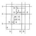
도 10을 이용하여 화상 처리 회로(502)에서 행하는 화상 처리의 구체적인 방법의 일례를 설명한다. 도 10에서는 화소수를 12×12로 한 표시 영역을 나타낸다.
화상 처리로서는, (1)피검출물의 그림자를 촬상한 데이터(촬상 데이터라고도 함)로부터의 피검출물의 위치의 추출, (2)연속적으로 취득한 피검출물의 위치 데이터로부터의 피검출물의 움직임의 검출, (3)피검출물의 움직임에 대응한 처리 등을 행한다.
먼저, (1)피검출물의 그림자의 촬상 데이터로부터 피검출물의 위치를 추출하는 방법에 대하여 설명한다. 예를 들면, 도 10의 두꺼운 선으로 나타낸 바와 같이, 표시 영역을 영역(2001), 영역(2002), 영역(2003), 및 영역(2004)의 4영역으로 분할하고, 각각의 영역에서의 피검출물의 그림자라고 인식되는 영역의 비율을 계수(計數)한다. 보다 구체적으로는, 각 화소의 포토 센서에서 취득한 광의 양이 특정의 스레숄드값보다 작은 경우에, 이 화소는 피검출물의 그림자로 되어 있는 것으로 한다.
그리고, 이 영역(2001 내지 2004)에 있어서, 전화소 중의 그림자가 되어 있는 화소의 비율이 가장 큰 영역을 피검출물의 위치로서 추출한다. 도 10에서는, 그림자가 되는 화소를 사선으로 나타낸다. 각 영역에서의 그림자가 되는 화소의 비율은, 영역(2001)에서는 25/36, 영역(2002)에서는 12/36, 영역(2003)에서는 3/36, 영역(2004)에서는 6/36이고, 영역(2001)에서 그림자가 되는 화소의 비율이 가장 크기 때문에, 영역(2001)을 피검출물의 위치로서 추출하여, 위치 데이터를 취득한다.
또한, 표시 영역의 분할수를 보다 많게 함으로써, 보다 치밀한 위치를 추출할 수 있다.
다음에, (2)연속적으로 취득한 피검출물의 위치 데이터로부터 피검출물의 움직임을 검출하는 방법에 대하여 설명한다. 예를 들면, 상기의 위치 데이터를 연속적으로 취득하고, 대상이 되는 위치 데이터와 전후의 위치 데이터를 비교함으로써, 피검출물의 움직임을 알 수 있다. 구체적으로는, 직전의 위치 데이터가 오른쪽, 이번의 위치 데이터가 왼쪽인 경우, 피검출물은 오른쪽에서 왼쪽으로 이동했다고 검출할 수 있다. 또한, 보다 치밀한 위치를 추출하는 경우에는, 피검출물의 이동 방향에 더하여, 이동의 속도 등, 보다 치밀한 움직임을 검출할 수도 있다.
계속하여, (3)피검출물의 움직임에 대응한 처리를 행하는 방법에 대하여 설명한다. 이 처리의 일례로서는, 피검출물의 움직임에 대응하여 표시를 제어하는 처리를 들 수 있다. 구체적으로는, 피검출물을 왼쪽에서 오른쪽으로 움직일 때에 동영상을 재생하는 처리, 또는 피검출물을 위에서 아래로 움직일 때에 동영상의 재생을 정지시키는 처리 등이 있다. 그리고, 피검출물의 움직임에 대응하여 이 처리를 행하기 위한 신호(입력 데이터)를 생성함으로써 처리가 행해진다.
또한, 이 처리의 다른 예로서는, 피검출물의 움직임의 궤적을 문자나 그림으로서 인식시키는 처리를 들 수 있다. 즉, 피검출물에 의해 그려진 문자나 그림을 신호(입력 데이터)로 할 수 있다. 또한, 피검출물의 움직임에 대응하여, 미리 설정된 문자나 그림을 판독해도 좋다.
또한, 포토 센서의 감도를, 광의 양에 따라 가변으로 하는 것이 효과적이다. 예를 들면, 도 2 또는 도 3의 구성에 있어서, 포토 센서에 인가하는 전위(포토 다이오드 리셋 신호선(108)의 전위, 게이트 신호선(209)의 전위, 포토 센서 기준 신호선(212)의 전위, 또는 프리차지 신호선(303)의 전위)를 변경함으로써, 감도를 가변으로 할 수 있다.
이와 같이, 포토 센서의 감도를 가변으로 함으로써, 표시 패널의 사용 환경(밝기 등)에 따라 최적의 감도로 설정할 수 있고, 비접촉의 피검출물의 그림자를 용이하게 판별할 수 있다. 또한, 비접촉의 피검출물의 그림자를 검출하는 것 외에, 표시 패널을 밀착형 에어리어 센서로서 이용하는 것도 가능하게 된다.
이상과 같은 형태로 함으로써, 비접촉의 피검출물에 대하여 검출 가능하게 되고, 데이터의 입력을 행하는 것이 가능한 표시 패널을 제공할 수 있다.
또한, 상기의 화상 처리는 피검출물의 그림자를 검출하는 경우뿐만 아니라, 피검출물로부터의 반사광을 이용하는 경우에도 적용할 수 있다. 반사광을 이용하는 경우, 피검출물이 접근하는 위치에 배치된 포토 센서는 다른 위치와 비교하여 강한 광을 받는다. 즉, 상기의 화상 처리를 적용하고, 표시 영역에서 강한 광을 수광한 영역을 특정함으로써, 피검출물의 위치, 움직임, 또는 형상을 검출할 수 있다. 이 경우, 도 10의 예에서 사선을 그린 화소는 피검출물로부터의 반사광에 보다 강한 광을 받은 화소가 된다.
또한, 표시 패널에 비접촉의 피검출물의 검출을 행하는 제 1 포토 센서와, 접촉한 피검출물의 검출을 행하는 제 2 포토 센서를 형성하는 것도 효과적이다. 제 2 포토 센서는 밀착형 에어리어 센서로서 이용하는 것이다. 이러한 구성으로 함으로써, 비접촉의 피검출물을 검출할 수 있는 표시 패널이면서, 접촉한 피검출물에 대해서도 검출할 수 있는 표시 패널을 제공할 수 있다. 즉, 용도에 따라 2개의 검출 기능을 나누어 사용할 수 있다.
제 1 포토 센서를 가지는 화소와 제 2 포토 센서를 가지는 화소가 각각 매트릭스 형상으로 표시 패널에 배치된다. 그때, 제 2 포토 센서의 수는 제 1 포토 센서의 수보다 많은 것이 바람직하다. 밀착형 에어리어 센서로서 이용하는 제 2 포토 센서는 촬상 화상에서 고해상도가 요구되기 때문에, 제 2 포토 센서의 간극(피치)을 좁게 함으로써 해상도를 높게 할 수 있다. 한편, 그림자를 검출하는 제 1 포토 센서는 피검출물의 위치를 판별할 수 있다면 충분하고, 밀착형 에어리어 센서로서 이용하는 제 2 포토 센서만큼의 높은 해상도가 필요없다. 즉, 제 2 포토 센서가 배치된 간극을 제 1 포토 센서가 배치된 간극보다 좁게 하면 좋다.
또한, 그림자를 검출하는 제 1 포토 센서를 형성하는 화소는 밀착형 에어리어 센서로서 이용하는 제 2 포토 센서가 빠진 화소가 된다. 따라서, 화상 처리에 의해 제 2 포토 센서가 빠진 화소의 화상을 복원할 수 있도록, 그림자를 검출하는 제 1 포토 센서의 주위 1∼3 화소 정도에는, 밀착형 에어리어 센서로서 이용하는 제 2 포토 센서를 형성하는 것이 바람직하다.
도 11(A)에, 그림자의 검출을 행하는 제 1 포토 센서와 밀착형 에어리어 센서로서 이용하는 제 2 포토 센서를 배치한 화소의 예를 나타낸다. 도 11(A) 및 도 11(B)에서는 화소수를 12×12로 하고 있지만, 이것에 한정되는 것은 아니다.
도 11(A)에서, 제 1 포토 센서는 사선으로 나타내는 화소에 배치되고, 그 외의 화소에 제 2 포토 센서가 배치되고, 각각이 간극을 취하여 매트릭스 형상으로 배치되어 있다. 상기의 이유로, 제 2 포토 센서의 수는 제 1 포토 센서의 수보다 많다.
또한, 도 11(A)과 같이 반드시 일정 간극을 취하여 배치되어 있을 필요는 없고, 도 11(B)과 같이 다른 간극으로 배치되어 있어도 좋다. 보다 실용적인 화소수로서 640×480을 이용한 경우, 10×10의 100 화소의 영역으로 분할하여 생각하면, 100 화소 중 1개에 제 1 포토 센서를 배치하고, 99개에 제 2 포토 센서를 배치함으로써, 피검출물의 그림자를 검출하면서, 밀착형 에어리어 센서로서의 기능을 충분히 할 수 있다. 단 이것에 한정되지 않고, 제 1 포토 센서와 제 2 포토 센서를 배치하는 비율은 검출 정밀도에 따라 결정하면 좋고, 예를 들면 제 1 포토 센서와 제 2 포토 센서를 같은 수로 하는 것도 가능하다.
또한, 그림자를 검출하는 제 1 포토 센서와 밀착형 에어리어 센서로서 이용하는 제 2 포토 센서에 있어서, 각각의 포토 센서에 인가하는 전위(예를 들면, 도 2 또는 도 3에서의 포토 다이오드 리셋 신호선(108)의 전위, 게이트 신호선(209)의 전위, 포토 센서 기준 신호선(212)의 전위, 또는 프리차지 신호선(303)의 전위)를 독립적으로 설정하는 것이 효과적이다. 또한, 각각의 포토 센서에 있어서, 포토 다이오드의 사이즈 또는 포토 센서의 회로 구성을 바꾸는 것이 효과적이다.
또한, 본 실시형태에서는, 표시 패널을 이용하는 장치에 대하여 설명했지만, 표시 패널을 이용하지 않는 장치로 해도 좋다. 그 경우, 피검출물이 접촉 또는 접근하는 부분(입력부라고도 함)에 포토 센서를 제공하고, 상기와 마찬가지로 화상 처리부 등을 형성하면 좋다.
본 실시형태는, 다른 실시형태 또는 실시예와 적절히 조합하여 실시할 수 있다.
(실시형태 2)
본 실시형태에서는, 피검출물로부터의 반사광을 이용하는 경우에, 포토 센서의 검출 정밀도를 높이는 방법을 설명한다.
비접촉의 피검출물을 검출하는 위해서는, 피검출물이 반사하는 미약한 광을 효과적으로 검출할 필요가 있다. 구체적으로는, 다음과 같은 구성이 있다.
적외광을 검출하는 센서(적외광 센서)를 포토 센서로서 표시 패널에 형성한다. 그리고, 표시 패널로부터 적외광을 조사하고, 피검출물에서 반사한 광을 이 적외광 센서에서 검출하는 구성으로 한다. 적외광 센서는 예를 들면, 수광 소자 위에 다른 색의 컬러 필터(예를 들면, R(적)과 B(청), R(적)과 G(녹) 등)를 중첩하여 형성하는 구조로 할 수 있다. 이러한 구조로 함으로써, 가시광 이외의 광(적외광)의 광을 수광 소자에 입사시킬 수 있다. 또한, 상기의 컬러 필터를, 컬러 표시를 행하기 위한 필터와 겸용함으로써, 공정수를 삭감할 수 있다. 또한, 백라이트에 가시광(백색)에 더하여 적외광을 발하는 광원도 더함으로써, 표시 패널로부터 적외광을 조사할 수 있다. 적외광은 가시광에 비하여 파장이 길고 산란이 적으므로, 검출 감도를 높이는 것이 용이하게 된다. 특히 피검출물이 사람의 손가락이나 손인 경우, 적외광을 검출하는 구성이 효과적이다.
적외광 센서와 가시광 센서를 다른 재료로 형성하는 경우, 적외광 센서에는 가시광 이외의 광(적외광)의 광을 흡수하는 재료로 센서를 형성하면 좋다. 예를 들면, InGaAs, PbS, 또는 PbSe 등에 의해 형성된 포토 센서는 효율적으로 적외광을 흡수한다.
실시형태 1에 설명한, 표시 패널에 비접촉의 피검출물의 검출을 행하는 제 1 포토 센서와, 접촉한 피검출물을 검출하는 제 2 포토 센서를 형성하는 구성에 있어서, 제 1 포토 센서를 적외광 센서로 하고, 제 2 포토 센서를 가시광 센서로 함으로써, 비접촉의 피검출물을 검출하는 기능과, 밀착형 에어리어 센서로서의 기능의, 양쪽의 정밀도를 높이는 것이 가능하게 된다. 제 1 포토 센서(적외광 센서) 및 제 2 포토 센서(가시광 센서)의 배치는 실시형태 1과 마찬가지로 행할 수 있다.
또한, 실시형태 1에 설명한 화상 처리를 적용할 수 있다.
본 실시형태는, 다른 실시형태 또는 실시예와 적절히 조합하여 실시할 수 있다.
(실시형태 3)
도 6에 표시 패널의 단면도의 일례를 나타낸다. 도 6에 나타낸 표시 패널에서는, 절연 표면을 가지는 기판(TFT 기판)(1001) 위에, 포토 다이오드(1002), 트랜지스터(1003), 보유 용량(1004), 액정 소자(1005)가 형성되어 있다.
포토 다이오드(1002)와 보유 용량(1004)은 트랜지스터(1003)를 제작하는 공정에서, 트랜지스터(1003)와 함께 형성하는 것이 가능하다. 포토 다이오드(1002)는 횡형 접합 타입의 pin 다이오드이고, 포토 다이오드(1002)가 가지는 반도체막(1006)은 p형의 도전성을 가지는 영역(p층)과, i형의 도전성을 가지는 영역(i층)과, n형의 도전성을 가지는 영역(n층)을 가진다. 또한, 본 실시형태에서는 포토 다이오드(1002)가 pin 다이오드인 경우를 예시하고 있지만, 포토 다이오드(1002)는 pn 다이오드이어도 좋다. 횡형 접합 타입의 pin 접합 또는 pn 접합은 p형을 부여하는 불순물과 n형을 부여하는 불순물을 각각 반도체막(1006)의 특정의 영역에 첨가함으로써 형성할 수 있다.
또한, TFT 기판(1001) 위에 성막한 하나의 반도체막을 에칭 등에 의해 소망의 형상으로 가공(패터닝)함으로써, 포토 다이오드(1002)의 섬형상의 반도체막과, 트랜지스터(1003)의 섬형상의 반도체막과, 보유 용량(1004)의 섬형상의 반도체막(하부 전극)을 함께 형성할 수 있다. 그렇게 함으로써, 제작 공정을 삭감하는 것이 가능하고, 비용을 저감할 수 있다.
또한, 횡형 접합 타입의 포토 다이오드로 하지 않고, p층, i층, 및 n층을 적층시킨 구조를 채용할 수도 있다.
액정 소자(1005)는 화소 전극(1007)과, 액정(1008)과, 대향 전극(1009)을 가진다. 화소 전극(1007)은 TFT 기판(1001) 위에 형성되어 있고, 트랜지스터(1003)와, 보유 용량(1004)과, 도전막(1010)을 통하여 전기적으로 접속되어 있다. 또한, 기판(대향 기판)(1013)에는 대향 전극(1009)이 형성되어 있고, 화소 전극(1007)과 대향 전극(1009)의 사이에, 액정(1008)이 끼워져 있다. 또한, 도 6에서는 포토 센서에 이용되는 트랜지스터에 대해서는 도시하지 않았지만, 이 트랜지스터도 트랜지스터(1003)를 제작하는 공정에서, 트랜지스터(1003)와 함께 TFT 기판(1001) 위에 형성하는 것이 가능하다.
화소 전극(1007)과 대향 전극(1009) 사이의 셀갭은 스페이서(1016)를 이용하여 제어할 수 있다. 도 6에서는 포토리소그래피에 의해 선택적으로 형성된 주상(柱狀)의 스페이서(1016)를 이용하여 셀갭을 제어하고 있지만, 구상(球狀)의 스페이서를 화소 전극(1007)과 대향 전극(1009)의 사이에 분산시킴으로써, 셀갭을 제어할 수도 있다.
또한, 액정(1008)은 TFT 기판(1001)과 대향 전극(1013)의 사이에서, 봉지재에 의해 둘러싸여 있다. 액정(1008)의 주입은 디스펜서식(적하식)을 이용해도 좋고, 딥핑식(펌핑식)을 이용해도 좋다.
화소 전극(1007)에는 투광성을 가지는 도전성 재료를 이용할 수 있다. 예를 들면, 인듐 주석 산화물(ITO), 산화규소를 포함하는 인듐 주석 산화물(ITSO), 유기 인듐, 유기 주석, 산화아연, 산화아연을 포함하는 인듐 아연 산화물(IZO), 갈륨을 포함하는 산화아연, 산화주석, 산화텅스텐을 포함하는 인듐 산화물, 산화텅스텐을 포함하는 인듐 아연 산화물, 산화티탄을 포함하는 인듐산화물, 산화티탄을 포함하는 인듐 주석 산화물 등을 이용할 수 있다.
또한, 본 실시형태에서는, 투과형의 액정 소자(1005)를 예로 들 수 있으므로, 화소 전극(1007)과 마찬가지로, 대향 전극(1009)에도 상술한 투광성을 가지는 도전성 재료를 이용할 수 있다.
화소 전극(1007)과 액정(1008)의 사이에는 배향막(1011)이, 대향 전극(1009)과 액정(1008)의 사이에는 배향막(1012)이, 각각 형성되어 있다. 배향막(1011), 배향막(1012)은 폴리이미드, 폴리비닐알코올 등의 유기 수지를 이용하여 형성할 수 있다. 그리고, 배향막(1011) 및 배향막(1012)의 표면은 러빙 등의 액정 분자를 일정 방향으로 배열시키기 위한 배향 처리가 실시되어 있다. 러빙은 배향막에 압력을 가하면서, 나일론 등의 천을 감은 롤러를 회전시켜, 상기 배향막의 표면을 일정 방향으로 문지름으로써 행할 수 있다. 또한, 산화규소 등의 무기 재료를 이용하여, 배향 처리를 실시하지 않고, 증착법으로 배향 특성을 가지는 배향막(1011), 배향막(1012)을 직접 형성하는 것도 가능하다.
또한, 액정 소자(1005)와 중첩되도록, 특정 파장 영역의 광을 통할 수 있는 컬러 필터(1014)가 대향 전극(1013)에 형성되어 있다. 컬러 필터(1014)는 안료를 분산시킨 아크릴계 수지 등의 유기 수지를 기판(1013) 위에 도포한 후, 포토리소그래피법을 이용하여 선택적으로 형성할 수 있다. 또한, 안료를 분산시킨 폴리이미드계 수지를 기판(1013) 위에 도포한 후, 에칭을 이용하여 선택적으로 형성할 수 있다. 혹은, 잉크 제트 등의 액적 토출법을 이용함으로써, 선택적으로 컬러 필터(1014)를 형성할 수 있다.
또한, 포토 다이오드(1002)와 중첩되도록, 광을 차폐할 수 있는 차폐막(1015)이 대향 전극(1013)에 형성되어 있다. 차폐막(1015)을 형성함으로써, 대향 전극(1013)을 투과하여 표시 패널 내에 입사한 광이 직접 포토 다이오드(1002)에 닿는 것을 막을 수 있다. 또한, 차폐막(1015)을 형성함으로써, 화소 간에 있어서의 액정(1008)의 배향의 흐트러짐에 기인하는 디스클리네이션(disclination)이 시인되는 것을 막을 수 있다. 차폐막(1015)에는 카본 블랙, 저차 산화티탄 등의 흑색 안료를 포함하는 유기 수지를 이용할 수 있다. 또는, 크롬을 이용한 막으로 차폐막(1015)을 형성하는 것도 가능하다.
또한, TFT 기판(1001)의 화소 전극(1007)이 형성되어 있는 면과는 반대 면에 편광판(1017)을 설치하고, 대향 전극(1013)의 대향 전극(1009)이 형성되어 있는 면과는 반대 면에 편광판(1018)을 형성한다.
액정 소자의 표시 모드는 TN(Twisted Namatic)형 외에, VA(Vertical Aligement)형, OCB(Optically Compensated Birefringence)형, IPS(In-Plane Switching)형 등이어도 좋다. 또한, 본 실시형태에서는 화소 전극(1007)과 대향 전극(1009)의 사이에 액정(1008)이 끼워져 있는 구조의 액정 소자(1005)를 예로 들어 설명하였지만, 본 발명의 일양태에 관한 표시 패널은 이 구성에 한정되지 않는다. IPS형과 같이, 한쌍의 전극이 모두 TFT 기판(1001)측에 형성되어 있는 액정 소자이어도 좋다.
또한, 본 실시형태에서는 포토 다이오드(1002), 트랜지스터(1003), 보유 용량(1004)에 박막의 반도체막을 이용하는 경우를 예로 들고 있지만, 단결정 반도체 기판, SOI 기판 등을 이용하여 형성되어 있어도 좋다.
백라이트로부터의 광은 대향 전극(1013)측으로부터 조사된다. 즉, 화살표(1020)로 나타낸 바와 같이 액정 소자(1005)를 통하여, TFT 기판(1001)측에 있는 피검출물(1021)에 조사된다. 그리고, 피검출물(1021)에서 반사된 광은 화살표(1022)로 나타낸 바와 같이, 포토 다이오드(1002)에 입사한다.
또한, 외광을 검출하는 경우, 외광은 TFT 기판(1001)측으로부터 조사된다. 피검출물(1021)에서 외광이 차단되기 때문에, 포토 다이오드(1002)로의 입사광이 차단된다. 즉, 포토 다이오드(1002)는 피검출물의 그림자를 검출하게 된다.
이상과 같은 형태의 표시 패널은 피검출물의 움직임을 검출함으로써, 데이터의 입력을 행할 수 있다.
또한, 본 실시형태의 표시 장치는 피검출물이 표시 패널로부터 근접한 거리에 있는 경우에도 검출하는 것이 가능하다. 그 거리는 3cm 이하로 할 수 있고, CCD 이미지 센서 등을 형성한 경우에 비하여 효과적이다.
또한, 본 실시형태의 표시 장치는 포토 센서(포토 다이오드(1002))의 수광면의 방향과, 표시 패널의 표시면(TFT 기판(1001)측)의 방향이 동일하다. 따라서, 표시 패널에서 피검출물을 촬상할 수 있고, CCD 이미지 센서 등을 형성한 경우에 비하여 효과적이다.
본 실시형태는, 다른 실시형태 또는 실시예와 적절히 조합하여 실시할 수 있다.
(실시형태 4)
도 7에, 실시형태 3과는 다른 표시 패널의 단면도의 일례를 나타낸다. 도 7에서는 포토 다이오드(1002)에 차폐막(2019)이 형성되어 있다. 그리고, 차폐막(2019)은 트랜지스터(1003)의 게이트 전극을 구성하는 도전막(1019)과 같은 재료를 이용하여, 도전막(1019)과 함께 구성된다. 포토 다이오드(1002)에 차폐막을 형성함으로써, 백라이트의 광이 수광부에 직접 입사하는 것을 회피할 수 있다. 따라서, 피검출물로부터의 반사광만을 효율적으로 검출할 수 있다.
또한, p형의 도전성을 가지는 영역(p층)과 n형의 도전성을 가지는 영역(n층)을 형성할 때에, 차폐막(2019)을 마스크로서 이용함으로써, 셀프얼라인으로 불순물을 첨가할 수 있다. 이것은 미세한 포토 다이오드를 작성할 때에 효과적이고, 화소 사이즈의 축소나 개구율의 향상에 효과적이다.
이러한 형태의 표시 패널에 있어서도, 실시형태 3과 마찬가지로, 피검출물의 움직임을 검출함으로써, 데이터의 입력을 행할 수 있다.
또한, 도 7에서는 횡형 접합 타입의 포토 다이오드를 채용하고 있지만, p층, i층, 및 n층을 적층시킨 구조를 채용할 수도 있다.
또한, 표시 패널의 그 외의 구조에 대하여, 포토 다이오드(1002)로의 입사광에 대하여, 피검출물과 표시 패널과의 거리, 및 포토 센서의 수광면과 표시 패널의 표시면과의 방향에 대해서는, 실시형태 3과 마찬가지이다.
본 실시형태는, 다른 실시형태 또는 실시예와 적절히 조합하여 실시할 수 있다.
(실시형태 5)
도 12에, 실시형태 3 및 실시형태 4와는 다른 표시 패널의 단면도의 다른 일례를 나타낸다. 도 12에서는, 백라이트로부터의 광이 TFT 기판(1001)측으로부터 조사하는 점에서, 도 6 및 도 7과 다르다. 즉, 화살표(2020)로 나타낸 바와 같이 액정 소자(1005)를 통하여, 대향 전극(1013)측에 있는 피검출물(1021)에 조사된다. 그리고, 피검출물(1021)에서 반사된 화살표(2022)로 나타낸 광이 포토 다이오드(1002)에 입사한다. 이 경우, 포토 다이오드(1002)의 상부의 차폐막(1015)에 개구를 형성하는 등, 피검출물(1021)에서 반사된 광이 포토 다이오드(1002)에 입사하도록 하면 좋다.
본 실시형태에서는, 포토 다이오드(1002)의 하부에 차폐막(2015)을 형성한다. 차폐막(2015)을 형성함으로써, TFT 기판(1001)을 투과하여 표시 패널 내에 입사한 백라이트로부터의 광이 직접 포토 다이오드(1002)에 닿는 것을 방지할 수 있고, 고정밀도의 화상 촬상이 가능한 표시 패널을 제공할 수 있다. 차폐막(2015)에는 카본 블랙, 저차 산화티탄 등의 흑색 안료를 포함하는 유기 수지를 이용할 수 있다. 또는, 크롬을 이용한 막으로 차폐막(2015)을 형성하는 것도 가능하다.
포토 다이오드(1002)에 있어서 적외광을 검출하는 경우, 포토 다이오드(1002) 위에 적외광을 투과시키는 컬러 필터(1014)를 형성하면 좋다. 그 경우, 다른 색의 컬러 필터의 적층 구조로 하는 것이 바람직하다.
또한, 도 12에서는 횡형 접합 타입의 포토 다이오드를 채용하고 있지만, p층, i층, 및 n층을 적층시킨 구조를 채용할 수도 있다.
또한, 외광을 검출하는 경우, 외광은 대향 전극(1013)측으로부터 조사된다. 피검출물(1021)에서 외광이 차단되기 때문에, 포토 다이오드(1002)로의 입사광이 차단된다. 즉, 포토 다이오드(1002)는 피검출물의 그림자를 검출하게 된다.
피검출물과 표시 패널과의 거리, 및 포토 센서의 수광면과 표시 패널의 표시면과의 방향에 대해서는, 실시형태 3과 마찬가지이다. 포토 센서의 수광면이 표시 패널의 표시면(대향 전극(1013)측)으로 향하고 있음으로써, 표시 패널에서 피검출물을 촬상할 수 있다.
본 실시형태는, 다른 실시형태 또는 실시예와 적절히 조합하여 실시할 수 있다.
[실시예 1]
본 실시예에서는 본 발명의 표시 패널에서의 패널과 광원의 배치에 대하여 설명한다. 도 8은 본 발명의 표시 패널의 구조를 나타낸 사시도의 일례이다. 도 8에 나타낸 표시 패널은 한쌍의 기판 사이에 액정 소자, 포토 다이오드, 박막 트랜지스터 등을 포함하는 화소가 형성된 패널(1601), 제 1 확산판(1602), 프리즘 시트(1603), 제 2 확산판(1604), 도광판(1605), 반사판(1606), 복수의 광원(1607)을 가지는 백라이트(1608), 회로 기판(1609)을 가진다.
패널(1601), 제 1 확산판(1602), 프리즘 시트(1603), 제 2 확산판(1604), 도광판(1605), 반사판(1606)은 순차로 적층되어 있다. 광원(1607)은 도광판(1605)의 단부에 형성되어 있고, 도광판(1605) 내부에 확산된 광원(1607)으로부터의 광은 제 1 확산판(1602), 프리즘 시트(1603) 및 제 2 확산판(1604)에 의해, 대향 기판측으로부터 균일하게 패널(1601)에 조사된다.
또한, 본 실시예에서는, 제 1 확산판(1602)과 제 2 확산판(1604)을 이용하고 있지만, 확산판의 수는 이것에 한정되지 않고, 단수이어도 3 이상이어도 좋다. 그리고, 확산판은 도광판(1605)과 패널(1601)의 사이에 설치되면 좋다. 따라서, 프리즘 시트(1603)보다 패널(1601)에 가까운 측에만 확산판이 설치되어 있어도 좋고, 프리즘 시트(1603)보다 도광판(1605)에 가까운 측에만 확산판이 설치되어 있어도 좋다.
또한, 프리즘 시트(1603)는 도 8에 도시한 단면이 톱니 모양의 형상에 한정되지 않고, 도광판(1605)으로부터의 광을 패널(1601)측으로 집광할 수 있는 형상을 가지면 좋다.
회로 기판(1609)에는 패널(1601)에 입력되는 각종 신호를 생성 혹은 처리하는 회로, 패널(1601)로부터 출력되는 각종 신호를 처리하는 회로 등이 설치되어 있다. 그리고 도 8에서는, 회로 기판(1609)과 패널(1601)이 FPC(Flexible Printed Circuit)(1611)를 통하여 접속되어 있다. 또한, 상기 회로는 COG(Chip On Glass)법을 이용하여 패널(1601)에 접속되어도 좋고, 상기 회로의 일부가 FPC(1611)에 COF(Chip On Film)법을 이용하여 접속되어도 좋다.
도 8에서는, 광원(1607)의 구동을 제어하는 제어계의 회로가 회로 기판(1609)에 설치되어 있고, 이 제어계의 회로와 광원(1607)이 FPC(1610)를 통하여 접속되어 있는 예를 나타낸다. 단, 상기 제어계의 회로는 패널(1601) 중에 형성되어 있어도 좋고, 이 경우는 패널(1601)과 광원(1607)과 이 FPC 등에 의해 접속되도록 한다.
또한, 도 8은 도광부(1605)의 단부에 광원(1607)이 배치되는 엣지라이트형(edge-Light type)의 광원을 예시하고 있지만, 본 발명의 표시 패널은 광원(1607)이 패널(1601)의 바로 아래에 배치되는 직하(直下)형이어도 좋다.
예를 들면, 피검출물인 손가락(1612)을 TFT 기판측으로부터 패널(1601)에 접근시키면, 백라이트(1608)로부터의 광이 패널(1601)을 통과하고, 그 일부가 손가락(1612)에서 반사하여, 다시 패널(1601)에 입사한다. 각색에 대응하는 광원(1607)을 순차로 점등시키고, 색마다 촬상 데이터를 취득함으로써, 피검출물인 손가락(1612)의 컬러의 촬상 데이터를 얻을 수 있다.
본 실시예는, 다른 실시형태 또는 실시예와 적절히 조합하여 실시할 수 있다.
[실시예 2]
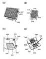
본 발명의 일양태에 관한 표시 패널은 비접촉으로 피검출물의 움직임을 검출함으로써, 데이터 입력을 행할 수 있다는 특징을 가진다. 따라서, 본 발명의 일양태에 관한 표시 패널을 이용한 전자 기기는 표시 패널을 그 구성 요소에 추가함으로써, 보다 고기능의 어플리케이션를 탑재할 수 있게 된다. 본 발명의 표시 패널은 표시 장치, 노트북형 퍼스널 컴퓨터, 기록 매체를 구비한 화상 재생 장치(대표적으로는 DVD:Digital Versatile Disc 등의 기록 매체를 재생하고, 그 화상을 표시할 수 있는 디스플레이를 가지는 장치)에 이용할 수 있다. 그 외에, 본 발명의 일양태에 관한 표시 패널을 이용할 수 있는 전자 기기로서, 휴대전화, 휴대형 게임기, 휴대 정보 단말, 전자서적, 비디오 카메라, 디지털 스틸 카메라, 고글형 디스플레이(헤드 마운트 디스플레이), 네비게이션 시스템, 음향 재생 장치(카 오디오, 디지털 오디오 플레이어 등), 복사기, 팩시밀리, 프린터, 프린터 복합기, 현금 자동 입출금기(ATM), 자동판매기 등을 들 수 있다. 이들 전자 기기의 구체예를 도 9에 나타낸다.
도 9(A)는 표시 장치로서, 하우징(5001), 표시부(5002), 지지대(5003) 등을 가진다. 본 발명의 일양태에 관한 표시 패널은 표시부(5002)에 이용할 수 있다. 표시부(5002)에 본 발명의 일양태에 관한 표시 패널을 이용함으로써, 고분해능의 촬상 데이터를 취득할 수 있고, 보다 고기능의 어플리케이션이 탑재된 표시 장치를 제공할 수 있다. 또한, 표시 장치에는, 퍼스널 컴퓨터용, TV 방송 수신용, 광고 표시용 등의 모든 정보 표시용 표시 장치가 포함된다.
도 9(B)는 휴대 정보 단말로서, 하우징(5101), 표시부(5102), 스위치(5103), 조작키(5104), 적외선 포트(5105) 등을 가진다. 본 발명의 일양태에 관한 표시 패널은 표시부(5102)에 이용할 수 있다. 표시부(5102)에 본 발명의 일양태에 관한 표시 패널을 이용함으로써, 고분해능의 촬상 데이터를 취득할 수 있고, 보다 고기능의 어플리케이션이 탑재된 휴대 정보 단말을 제공할 수 있다.
도 9(C)는 현금 자동 입출금기로서, 하우징(5201), 표시부(5202), 동전 투입구(5203), 지폐 투입구(5204), 카드 투입구(5205), 통장 투입구(5206) 등을 가진다. 본 발명의 일양태에 관한 표시 패널은 표시부(5202)에 이용할 수 있다. 표시부(5202)에 본 발명의 일양태에 관한 표시 패널을 이용함으로써, 고분해능의 촬상 데이터의 취득할 수 있고, 보다 고기능의 어플리케이션이 탑재된 현금 자동 입출금기를 제공할 수 있다. 그리고, 본 발명의 일양태에 관한 표시 패널을 이용한 현금 자동 입출금기는, 지문, 얼굴, 손도장, 장문(掌紋) 및 손의 정맥의 형상, 홍채 등의, 생체 인증에 이용되는 생체 정보의 판독을, 보다 고정밀도로 행할 수 있다. 따라서, 생체 인증에 있어서, 본인임에도 불구하고 본인이 아니라고 오인식되는 타인 거부율과, 타인임에도 불구하고 본인이라고 오인식하게 되는 타인 수락률을 낮게 억제할 수 있다.
도 9(D)는 휴대형 게임기로서, 하우징(5301), 하우징(5302), 표시부(5303), 표시부(5304), 마이크로폰(5305), 스피커(5306), 조작키(5307), 스타일러스(5308) 등을 가진다. 본 발명의 일양태에 관한 표시 패널은 표시부(5303) 또는 표시부(5304)에 이용할 수 있다. 표시부(5303) 또는 표시부(5304)에 본 발명의 일양태에 관한 표시 패널을 이용함으로써, 고분해능의 촬상 데이터를 취득할 수 있고, 보다 고기능의 어플리케이션이 탑재된 휴대형 게임기를 제공할 수 있다. 또한, 도 9(D)에 나타낸 휴대형 게임기는 2개의 표시부(5303)와 표시부(5304)를 가지지만, 휴대형 게임기가 가지는 표시부의 수는 이것에 한정되지 않는다.
또한, 지문 인식 장치 등과 같이 표시 패널을 필수로 하지 않는 장치에도 본 발명을 적용하는 것이 가능하다. 이 장치는 포토 센서가 제공된 입력부를 가지고, 입력부에 접촉 또는 접근하는 피검출물을 포토 센서에 의해 검출할 수 있다.
본 실시예는, 다른 실시형태 또는 실시예와 적절히 조합하여 실시할 수 있다.
[실시예 3]
본 실시예에서는, 전자 기기의 일례에 대하여, 도 13을 이용하여 설명한다.
도 13은 라이팅 보드(블랙 보드, 화이트 보드 등)이다. 본체(9001)의 라이팅부(9101)에 본 발명의 일양태에 관한 표시 패널 등의 입력부를 형성할 수 있다.
여기서, 라이팅부(9101)의 표면에는 마커 등을 이용하여 자유롭게 기입할 수 있다.
또한, 정착제가 포함되지 않은 마커 등을 이용하면 문자의 소거가 용이하다.
또한, 마커의 잉크를 제거하기 쉽기 때문에, 라이팅부(9101)의 표면은 충분한 평활성을 가지고 있으면 좋다.
예를 들면, 라이팅부(9101)의 표면이 유리 기판 등이라면 평활성은 충분하다.
또한, 라이팅부(9101)의 표면에 투명한 합성 수지 시트 등을 부착해도 좋다.
합성 수지로서는 예를 들면 아크릴 등을 이용하면 바람직하다. 이 경우, 합성 수지 시트의 표면을 평활하게 해 두면 바람직하다.
또한, 라이팅부(9101)가 특정 표시를 행할 때에, 표면에 그림이나 문자를 기재할 수 있다. 그리고, 라이팅부(9101)는 기재된 그림이나 문자로 표시된 화상을 합성할 수 있다.
더욱이, 포토 센서를 이용하고 있기 때문에, 기재한 후, 시간이 경과한 경우에도 언제라도 센싱이 가능하지만, 저항막 방식, 정전 용량 방식 등을 이용한 경우, 기재와 동시에 센싱할 수밖에 없다.
본 실시예는, 다른 실시형태 또는 실시예와 적절히 조합하여 실시할 수 있다.Hereinafter, embodiments will be described in detail with reference to the drawings. However, it will be understood by those skilled in the art that the following embodiments can be implemented in many different modes, and that various changes in form and details can be made without departing from the spirit and scope thereof. Therefore, the present invention is not limited to the description of the embodiments described below. In all the drawings for explaining the embodiments, the same reference numerals are given to the same parts or portions having the same functions, and the repetitive description thereof will be omitted.
(Embodiment 1)
In the present embodiment, an example of a display panel will be described.
1 is an example of the configuration of the display panel. The
The
In addition, the case where the
The
The display
The
A circuit diagram of the
One of the source and the drain of the
The
One electrode of the photodiode 204 is electrically connected to the photodiode
Next, the configuration of the photo
The
Next, the reading operation of the photosensor in the display panel will be described with reference to the timing chart of Fig. In FIG. 4, the
At time A, when the potential of the photodiode reset signal line 108 (signal 401) is set to "H" (reset operation), the photodiode 204 becomes conductive and the gate of the
At the time B, when the potential of the photodiode reset signal line 108 (signal 401) is set to "L" (cumulative operation), the gate of the
At the time C, when the potential of the gate signal line 209 (signal 402) is set to "H" (selection operation), the
At time D, when the potential of the gate signal line 209 (signal 402) is set to "L ", the
As described above, by knowing the magnitude of the amount of light irradiated to the photodiode 204, it is possible to detect whether the external light is incident or whether the external light is blocked by the non-contact object, that is, It can be judged whether or not it is.
Fig. 5 shows a display panel system 500 for detecting the movement of the object to be detected from the shadow of the object to be detected in the non-contact object to be detected. The display panel system 500 has a
An example of a specific method of image processing performed by the
The image processing includes (1) extraction of the position of the object to be detected from data (also referred to as image pickup data) of a shadow of the object to be detected, (2) detection of movement of the object to be detected from the position data of the object, (3) Processing corresponding to the movement of the object to be detected.
First, (1) a method of extracting the position of the object to be detected from the imaging data of the shadow of the object to be detected will be described. For example, as shown by the thick line in FIG. 10, the display region is divided into four regions, that is, the
In this
In addition, by making the number of divisions of the display area larger, it is possible to extract a more precise position.
Next, a method of detecting the motion of the object to be detected from the position data of the object to be detected continuously acquired (2) will be described. For example, the movement of the object to be detected can be known by continuously acquiring the above-mentioned position data and comparing the object position data with the front and rear position data. More specifically, when the immediately preceding position data is on the right and the current position data is on the left, it can be detected that the object to be detected has moved from right to left. Further, in the case of extracting a more precise position, it is also possible to detect a more dense movement such as a moving speed in addition to the moving direction of the object to be detected.
Next, (3) a method of performing processing corresponding to the movement of the object to be detected will be described. As an example of this process, there is a process for controlling the display in accordance with the motion of the object to be detected. Specifically, there is a process of reproducing moving images when the detected object is moved from left to right, or a process of stopping the reproduction of moving images when the detected object is moved from the top to the bottom. Then, processing is performed by generating a signal (input data) for performing this processing in accordance with the motion of the detected object.
Another example of this process is a process of recognizing the locus of movement of the object to be detected as a character or a figure. That is, a character or figure drawn by the object to be detected can be a signal (input data). It is also possible to read predetermined characters or pictures corresponding to the motion of the detected object.
It is also effective to make the sensitivity of the photosensor variable according to the amount of light. 2 or 3, the potential applied to the photosensor (the potential of the photodiode
Thus, by varying the sensitivity of the photosensor, it is possible to set the sensitivity to the optimum sensitivity according to the use environment (brightness, etc.) of the display panel, and to easily identify the shadow of the non-contact object to be detected. Further, in addition to detecting the shadow of the object to be detected that is not in contact, the display panel can be used as a contact type area sensor.
According to the above-described configuration, it is possible to provide a display panel capable of detecting data on a non-contact object and inputting data.
The above-described image processing can be applied not only to the case of detecting the shadow of the object to be detected, but also to the case of using reflected light from the object to be detected. In the case of using reflected light, the photosensor disposed at a position where the object to be detected comes closer receives strong light as compared with other positions. That is, the position, motion, or shape of the object to be detected can be detected by applying the above-described image processing and specifying an area where strong light is received in the display area. In this case, in the example of Fig. 10, the pixel drawn by the oblique line becomes a pixel which receives stronger light in the reflected light from the object to be detected.
It is also effective to form a first photosensor for detecting the object to be detected in contact with the display panel and a second photosensor for detecting the object to be detected in contact with the display panel. The second photosensor is used as a contact area sensor. With this configuration, it is possible to provide a display panel that can detect not only a display panel that can detect a non-contact object, but also a contacted object to be detected. That is, two detection functions can be used in accordance with the use.
A pixel having a first photosensor and a pixel having a second photosensor are arranged in a matrix on the display panel. At this time, it is preferable that the number of the second photosensors is larger than the number of the first photosensors. Since the second photosensor used as the contact type area sensor requires a high resolution in the captured image, the resolution can be increased by narrowing the gap (pitch) of the second photosensor. On the other hand, it is sufficient if the first photosensor for detecting shadows can determine the position of the object to be detected, and does not need as high a resolution as the second photosensor used as the contact area sensor. That is, the gap in which the second photosensor is disposed may be made narrower than the gap in which the first photosensor is disposed.
The pixels forming the first photosensor for detecting shadows are pixels missing the second photosensor used as the contact area sensor. Therefore, a second photosensor used as a close-up type area sensor is formed at about 1 to 3 pixels around the first photosensor for detecting shadows so that the image of the missing pixel of the second photosensor can be restored by the image processing .
11 (A) shows an example of a pixel in which a first photosensor for detecting shadows and a second photosensor for use as a close-up area sensor are arranged. 11A and 11B, the number of pixels is 12 x 12, but the present invention is not limited to this.
In Fig. 11A, the first photosensor is arranged in a pixel indicated by oblique lines, the second photosensor is arranged in the other pixels, and each of them is arranged in a matrix form with a gap therebetween. For the above reason, the number of the second photosensors is larger than the number of the first photosensors.
In addition, it is not always necessary to arrange them with a certain gap as shown in Fig. 11 (A), and they may be arranged with different gaps as shown in Fig. 11 (B). When 640 x 480 is used as a more practical number of pixels, considering dividing the area into 100 pixels of 10 x 10, if the first photosensor is arranged in one of 100 pixels and the second photosensor is arranged in 99 pixels , It is possible to sufficiently function as a close-contact type area sensor while detecting the shadow of the object to be detected. The ratio of the first photosensor and the second photosensor may be determined according to the detection accuracy. For example, the first photosensor and the second photosensor may be arranged in the same number.
In addition, in the first photosensor for detecting shadows and the second photosensor for use as a contact area sensor, the potential applied to each photosensor (for example, the photodiode reset signal line 108 (The potential of the
In the present embodiment, an apparatus using a display panel has been described, but an apparatus that does not use a display panel may be used. In this case, a photosensor may be provided at a portion where the object to be detected comes into contact with or approaches (also referred to as an input portion), and an image processing portion or the like may be formed in the same manner as described above.
This embodiment mode can be implemented in appropriate combination with another embodiment mode or embodiment.
(Embodiment 2)
In this embodiment, a method of increasing the detection accuracy of the photosensor when reflected light from the object to be detected is used will be described.
In order to detect a non-contact object to be detected, it is necessary to effectively detect weak light reflected by the object to be detected. Specifically, there is the following configuration.
A sensor (infrared light sensor) for detecting infrared light is formed on the display panel as a photosensor. Then, infrared light is irradiated from the display panel, and light reflected by the object to be detected is detected by the infrared light sensor. The infrared light sensor may have a structure in which color filters of different colors (for example, R (red) and B (blue), R (red) and G (green) . With this structure, light of light (infrared light) other than visible light can be incident on the light receiving element. Further, by using the color filter as a filter for color display, the number of steps can be reduced. In addition, by adding a light source that emits infrared light in addition to visible light (white) to the backlight, infrared light can be emitted from the display panel. Since infrared light has a longer wavelength and less scattering than visible light, it is easy to increase detection sensitivity. In particular, when the object to be detected is a finger or a hand of a person, a configuration for detecting infrared light is effective.
When the infrared light sensor and the visible light sensor are formed of different materials, the infrared light sensor may be formed of a material that absorbs light other than visible light (infrared light). For example, a photosensor formed by InGaAs, PbS, PbSe, or the like efficiently absorbs infrared light.
In the configuration described in
In addition, the image processing described in
This embodiment mode can be implemented in appropriate combination with another embodiment mode or embodiment.
(Embodiment 3)
6 shows an example of a sectional view of the display panel. In the display panel shown in Fig. 6, a
The
The semiconductor film of the island shape of the
Further, a structure in which a p-layer, an i-layer, and an n-layer are laminated instead of a lateral junction type photodiode may be adopted.
The
The cell gap between the
Further, the
The
In addition, in the present embodiment, a transmissive
An
A
A
A
The display mode of the liquid crystal element may be a VA (Vertical Alignment) type, an OCB (Optically Compensated Birefringence) type, or an IPS (In-Plane Switching) type in addition to a TN (Twisted Namatic) type. In the present embodiment, the
In the present embodiment, a thin film semiconductor film is used for the
Light from the backlight is irradiated from the side of the
When external light is detected, external light is irradiated from the
The display panel of the above-described type can perform data input by detecting the movement of the object to be detected.
Further, the display apparatus of the present embodiment can detect even when the object to be detected is at a short distance from the display panel. The distance can be 3 cm or less, which is more effective than the case where a CCD image sensor or the like is formed.
In the display device of the present embodiment, the direction of the light receiving surface of the photosensor (photodiode 1002) is the same as the direction of the display surface (on the
This embodiment mode can be implemented in appropriate combination with another embodiment mode or embodiment.
(Fourth Embodiment)
Fig. 7 shows an example of a cross-sectional view of a display panel different from that of the third embodiment. In Fig. 7, a
When forming the p-type conductivity (p-layer) and the n-type conductivity (n-layer), impurities can be added to the self-aligning film by using the
In this type of display panel, similarly to the third embodiment, data can be input by detecting the movement of the object to be detected.
Although a photodiode of a lateral junction type is employed in Fig. 7, a structure in which a p-layer, an i-layer, and an n-layer are stacked may be employed.
With respect to the other structures of the display panel, with respect to the incident light to the
This embodiment mode can be implemented in appropriate combination with another embodiment mode or embodiment.
(Embodiment 5)
Fig. 12 shows another example of a cross-sectional view of a display panel different from the third and fourth embodiments. 12 differs from FIG. 6 and FIG. 7 in that light from the backlight is emitted from the
In the present embodiment, a
In the case of detecting infrared light in the
Although a photodiode of a lateral junction type is employed in Fig. 12, a structure in which a p-layer, an i-layer and an n-layer are stacked may be employed.
When external light is detected, external light is irradiated from the
The distance between the object to be detected and the display panel and the direction of the light receiving surface of the photosensor and the display surface of the display panel are the same as those in the third embodiment. Since the light receiving surface of the photo sensor is directed to the display surface (opposite
This embodiment mode can be implemented in appropriate combination with another embodiment mode or embodiment.
[Example 1]
In this embodiment, the arrangement of the panel and the light source in the display panel of the present invention will be described. 8 is an example of a perspective view showing the structure of the display panel of the present invention. The display panel shown in Fig. 8 includes a
The
Although the
The
The
8 shows an example in which the circuit of the control system for controlling the driving of the
8 illustrates an edge-light type light source in which a
For example, when a
The present embodiment can be carried out by appropriately combining with other embodiments or embodiments.
[Example 2]
The display panel according to one aspect of the present invention is characterized in that data can be input by detecting the movement of the object to be detected in a noncontact manner. Therefore, in the electronic device using the display panel according to one aspect of the present invention, by adding the display panel to its constituent elements, a higher-performance application can be mounted. The display panel of the present invention can be applied to a display device, a notebook type personal computer, an image reproducing device provided with a recording medium (typically, a device having a display capable of reproducing a recording medium such as a DVD: Digital Versatile Disc, ). In addition to the above, an electronic device that can use a display panel according to an aspect of the present invention is a portable phone, a portable game machine, a portable information terminal, an electronic book, a video camera, a digital still camera, a goggle type display (head mount display) System, an audio reproducing device (car audio, a digital audio player, etc.), a copying machine, a facsimile, a printer, a multifunctional printer, an automatic teller machine (ATM), and a vending machine. Specific examples of these electronic devices are shown in Fig.
Fig. 9A shows a display device, which has a
9B is a portable information terminal having a
9C is a cash automatic teller machine including a
9D is a portable game machine including a
In addition, the present invention can be applied to an apparatus that does not require a display panel such as a fingerprint recognition apparatus or the like. This apparatus has an input section provided with a photosensor, and can detect the object to be contacted or approaching the input section with the photosensor.
The present embodiment can be carried out by appropriately combining with other embodiments or embodiments.
[Example 3]
In this embodiment, an example of an electronic apparatus will be described with reference to Fig.
13 is a lighting board (black board, white board, etc.). An input section such as a display panel according to an embodiment of the present invention can be formed in the
Here, the surface of the
In addition, when a marker or the like not containing a fixing agent is used, the character can be easily erased.
Further, since the ink of the marker is easily removed, it is sufficient that the surface of the
For example, if the surface of the
A transparent synthetic resin sheet or the like may be attached to the surface of the
As the synthetic resin, acrylic or the like is preferably used, for example. In this case, it is preferable to smooth the surface of the synthetic resin sheet.
Further, when the
Furthermore, since the photosensor is used, it is possible to sense at any time after elapse of time after the description, but when using the resistive film type, the electrostatic capacity type, or the like, it is inevitable to sense the film simultaneously with the substrate.
The present embodiment can be carried out by appropriately combining with other embodiments or embodiments.
100:표시 패널101:화소 회로
102:표시 소자 제어 회로 103:포토 센서 제어 회로
104:화소 105:표시 소자
106:포토 센서 107:표시 소자 구동 회로
108:표시 소자 구동 회로 109:포토 센서 판독 회로
110:포토 센서 구동 회로 201:트랜지스터
202:보유 용량203:액정 소자
204:포토 다이오드205:트랜지스터
206:트랜지스터207:게이트 신호선
208:포토 다이오드 리셋 신호선 209:게이트 신호선
210:비디오 데이터 신호선 211:포토 센서 출력 신호선
212:포토 센서 기준 신호선 213:게이트 신호선
300:포토 센서 판독 회로 301:p형 트랜지스터
302:보유 용량303:프리차지 신호선
401:신호 402:신호
403:신호 404:신호
405:신호 1001:기판
1002:포토 다이오드1003:트랜지스터
1004:보유 용량1005:액정 소자
1006:반도체막1007:화소 전극
1008:액정 1009:대향 전극
1010:도전막1011:배향막
1012:배향막1013:기판
1014:컬러 필터 1015:차폐막
1016:스페이서 1017:편광판
1018:편광판 1019:도전막
1020:화살표 1021:피검출물
1022:화살표 1601:패널
1602:제 1 확산판 1603:프리즘 시트
1604:제 2 확산판 1605:도광판
1606:반사판 1607:광원
1608:백라이트1609:회로 기판
1610:FPC1611:FPC
1612:손가락2015:차폐막
2019:차폐막 2020:화살표
2022:화살표 5001:하우징
5002:표시부5003:지지대
5101:하우징 5102:표시부
5103:스위치 5104:조작키
5105:적외선 포트5201:하우징
5202:표시부5203:동전 투입구
5204:지폐 투입구 5205:카드 투입구
5206:통장 투입구 5301:하우징
5302:하우징 5303:표시부
5304:표시부5305:마이크로폰
5306:스피커 5307:조작키
5308:스타일러스9001:본체
9101:라이팅부100: display panel 101: pixel circuit
102: display element control circuit 103: photosensor control circuit
104: pixel 105: display element
106: Photoelectric sensor 107: Display element driving circuit
108: Display element driving circuit 109: Photo sensor reading circuit
110: photo sensor drive circuit 201: transistor
202: storage capacitor 203: liquid crystal element
204: photodiode 205: transistor
206: transistor 207: gate signal line
208: photodiode reset signal line 209: gate signal line
210: video data signal line 211: photosensor output signal line
212: photo sensor reference signal line 213: gate signal line
300: photo sensor reading circuit 301: p-type transistor
302: Holding capacitor 303: Precharge signal line
401: Signal 402: Signal
403: Signal 404: Signal
405: signal 1001: substrate
1002: photodiode 1003: transistor
1004: Storage capacity 1005: Liquid crystal element
1006: Semiconductor film 1007: Pixel electrode
1008: liquid crystal 1009: counter electrode
1010: conductive film 1011: alignment film
1012: Orientation film 1013:
1014: color filter 1015: shielding film
1016: Spacer 1017: Polarizer
1018: polarizer 1019: conductive film
1020: arrow 1021: object to be detected
1022: arrow 1601: panel
1602: first diffusion plate 1603: prism sheet
1604: second diffusion plate 1605: light guide plate
1606: reflector 1607: light source
1608: backlight 1609: circuit board
1610: FPC 1611: FPC
1612: finger 2015: shielding film
2019: shielding film 2020: arrow
2022: arrow 5001: housing
5002: Display portion 5003: Support
5101: Housing 5102:
5103: switch 5104: operation key
5105: Infrared port 5201: Housing
5202: Display section 5203: Coin input port
5204: bill slot 5205: card slot
5206: passbook entry slot 5301: housing
5302: Housing 5303: Display
5304: Display section 5305: Microphone
5306: Speaker 5307: Operation keys
5308: Stylus 9001: Body
9101:
Claims (23)
Translated fromKorean각각 제 1 포토 센서를 포함하는 복수의 제 1 화소를 포함하는 광검출부와, 각각 제 2 포토 센서를 포함하는 복수의 제 2 화소를 포함하는 에어리어 센서부를 포함하는 표시 패널; 및
상기 표시 패널에 동작가능하게 접속된 화상 처리부를 포함하고,
상기 제 1 포토 센서는 상기 표시 패널과 접촉하지 않는 제 1 피검출물의 그림자를 검출하고,
상기 제 2 포토 센서는 상기 표시 패널과 접촉하는 제 2 피검출물을 검출하고,
상기 화상 처리부는 상기 제 1 포토 센서에 의해 얻어진 상기 제 1 피검출물의 상기 그림자의 데이터를 사용하여 상기 제 1 피검출물의 위치를 검출할 수 있고,
상기 복수의 제 2 화소로부터 선택된 두 개의 인접한 제 2 화소 사이의 피치는 상기 복수의 제 1 화소로부터 선택된 두 개의 인접한 제 1 화소 사이의 피치보다 짧은, 표시 장치.
In the display device,
A display panel including an optical sensor portion including a plurality of first pixels each including a first photosensor, and an area sensor portion including a plurality of second pixels each including a second photosensor; And
And an image processing section operably connected to the display panel,
The first photosensor detects a shadow of the first object to be detected which is not in contact with the display panel,
The second photosensor detects a second object to be detected which is in contact with the display panel,
The image processing section can detect the position of the first object to be detected by using the data of the shadow of the first object to be detected obtained by the first photosensor,
And a pitch between two adjacent second pixels selected from the plurality of second pixels is shorter than a pitch between two adjacent first pixels selected from the plurality of first pixels.
상기 화상 처리부는 상기 제 1 포토 센서에 의해 얻어진 상기 제 1 피검출물의 상기 그림자의 상기 데이터를 사용하여 상기 제 1 피검출물의 움직임을 검출할 수 있는, 표시 장치.
10. The method of claim 9,
Wherein the image processing section can detect the movement of the first object to be detected by using the data of the shadow of the first object to be detected obtained by the first photosensor.
각각 제 1 포토 센서를 포함하는 복수의 제 1 화소를 포함하는 광검출부와, 각각 제 2 포토 센서를 포함하는 복수의 제 2 화소를 포함하는 에어리어 센서부를 포함하는 복수의 영역을 포함하는 표시 패널; 및
상기 표시 패널에 동작가능하게 접속된 화상 처리부를 포함하고,
상기 제 1 포토 센서는 상기 표시 패널과 접촉하지 않는 제 1 피검출물의 그림자를 검출하고,
상기 제 2 포토 센서는 상기 표시 패널과 접촉하는 제 2 피검출물을 검출하고,
상기 화상 처리부는 상기 제 1 피검출물의 위치로서 상기 복수의 영역 중 다른 영역보다 많은 양의 그림자가 검출되는 복수의 영역 중의 하나를 인식할 수 있고,
상기 복수의 제 2 화소로부터 선택된 두 개의 인접한 제 2 화소 사이의 피치는 상기 복수의 제 1 화소로부터 선택된 두 개의 인접한 제 1 화소 사이의 피치보다 짧은, 표시 장치.
In the display device,
A display panel including a plurality of regions including an optical sensor portion including a plurality of first pixels each including a first photosensor and an area sensor portion including a plurality of second pixels each including a second photosensor; And
And an image processing section operably connected to the display panel,
The first photosensor detects a shadow of the first object to be detected which is not in contact with the display panel,
The second photosensor detects a second object to be detected which is in contact with the display panel,
The image processing section can recognize one of a plurality of regions in which a larger amount of shadows than the other regions are detected as the position of the first object to be detected,
And a pitch between two adjacent second pixels selected from the plurality of second pixels is shorter than a pitch between two adjacent first pixels selected from the plurality of first pixels.
상기 화상 처리부는 상기 제 1 포토 센서에 의해 얻어진 상기 제 1 피검출물의 상기 위치의 연속 데이터를 사용하여 상기 제 1 피검출물의 움직임을 검출할 수 있는, 표시 장치.
16. The method of claim 15,
Wherein the image processing section is capable of detecting the movement of the first object to be detected using continuous data of the position of the first object to be detected obtained by the first photosensor.
상기 복수의 제 2 화소의 갯수는 상기 복수의 제 1 화소의 갯수보다 많은, 표시 장치.
16. The method according to claim 9 or 15,
Wherein the number of the plurality of second pixels is larger than the number of the plurality of first pixels.
상기 복수의 제 1 화소는 상기 복수의 제 2 화소 둘레에 배열된, 표시 장치.
16. The method according to claim 9 or 15,
And the plurality of first pixels are arranged around the plurality of second pixels.
상기 제 1 포토 센서는 적외광 센서인, 표시 장치.
16. The method according to claim 9 or 15,
Wherein the first photosensor is an infrared light sensor.
상기 제 2 포토 센서는 가시광 센서인, 표시 장치.
16. The method according to claim 9 or 15,
And the second photosensor is a visible light sensor.
상기 제 1 포토 센서 및 상기 제 2 포토 센서 각각은
하나의 전극이 제 1 신호선에 전기적으로 접속되는 광 검출기;
소스 및 드레인 중 하나가 제 2 신호선에 전기적으로 접속되는 제 1 트랜지스터; 및
게이트가 게이트 신호선에 전기적으로 접속되는 제 2 트랜지스터를 포함하고,
상기 제 1 신호선, 상기 제 2 신호선, 및 상기 게이트 신호선 중 적어도 하나의 전위는 상기 제 1 포토 센서 및 상기 제 2 포토 센서 각각에서 개별적으로 설정되는, 표시 장치.
16. The method according to claim 9 or 15,
Each of the first photosensor and the second photosensor
A photodetector in which one electrode is electrically connected to the first signal line;
A first transistor having one of a source and a drain electrically connected to a second signal line; And
And a second transistor whose gate is electrically connected to the gate signal line,
Wherein a potential of at least one of the first signal line, the second signal line, and the gate signal line is set individually in each of the first photosensor and the second photosensor.
상기 제 1 포토 센서 및 상기 제 2 포토 센서 각각은 광 검출기를 포함하고,
상기 광 검출기는 포토 다이오드를 포함하는, 표시 장치.
16. The method according to claim 9 or 15,
Wherein each of said first photosensor and said second photosensor comprises a photodetector,
Wherein the photodetector comprises a photodiode.
Applications Claiming Priority (3)
| Application Number | Priority Date | Filing Date | Title |
|---|---|---|---|
| JP2009245530 | 2009-10-26 | ||
| JPJP-P-2009-245530 | 2009-10-26 | ||
| PCT/JP2010/067295WO2011052343A1 (en) | 2009-10-26 | 2010-09-27 | Display device and semiconductor device |
Related Child Applications (1)
| Application Number | Title | Priority Date | Filing Date |
|---|---|---|---|
| KR1020177017127ADivisionKR101843561B1 (en) | 2009-10-26 | 2010-09-27 | Display device and semiconductor device |
Publications (2)
| Publication Number | Publication Date |
|---|---|
| KR20120098737A KR20120098737A (en) | 2012-09-05 |
| KR101751902B1true KR101751902B1 (en) | 2017-06-28 |
Family
ID=43897996
Family Applications (2)
| Application Number | Title | Priority Date | Filing Date |
|---|---|---|---|
| KR1020127013230AExpired - Fee RelatedKR101751902B1 (en) | 2009-10-26 | 2010-09-27 | Display device and semiconductor device |
| KR1020177017127AExpired - Fee RelatedKR101843561B1 (en) | 2009-10-26 | 2010-09-27 | Display device and semiconductor device |
Family Applications After (1)
| Application Number | Title | Priority Date | Filing Date |
|---|---|---|---|
| KR1020177017127AExpired - Fee RelatedKR101843561B1 (en) | 2009-10-26 | 2010-09-27 | Display device and semiconductor device |
Country Status (7)
| Country | Link |
|---|---|
| US (1) | US20110096009A1 (en) |
| EP (1) | EP2494427A4 (en) |
| JP (2) | JP5710932B2 (en) |
| KR (2) | KR101751902B1 (en) |
| CN (1) | CN102612677B (en) |
| TW (1) | TWI517008B (en) |
| WO (1) | WO2011052343A1 (en) |
Families Citing this family (49)
| Publication number | Priority date | Publication date | Assignee | Title |
|---|---|---|---|---|
| TWI433310B (en)* | 2009-07-02 | 2014-04-01 | Au Optronics Corp | Organic light emitting diode touch display |
| KR101719587B1 (en)* | 2010-10-29 | 2017-03-27 | 삼성디스플레이 주식회사 | Organic Light Emitting Display having Touch Screen Funtion |
| KR101843559B1 (en)* | 2010-11-05 | 2018-03-30 | 가부시키가이샤 한도오따이 에네루기 켄큐쇼 | Display device with imaging function and method for driving the same |
| JP2012256020A (en) | 2010-12-15 | 2012-12-27 | Semiconductor Energy Lab Co Ltd | Semiconductor device and driving method for the same |
| KR102021908B1 (en)* | 2011-05-03 | 2019-09-18 | 삼성전자주식회사 | Optical touch screen apparatus and method of driving the optical touch screen apparatus |
| JP6057407B2 (en)* | 2012-02-22 | 2017-01-11 | 学校法人東京電機大学 | Touch position input device and touch position input method |
| US9817520B2 (en)* | 2013-05-20 | 2017-11-14 | Semiconductor Energy Laboratory Co., Ltd. | Imaging panel and imaging device |
| US9256290B2 (en) | 2013-07-01 | 2016-02-09 | Blackberry Limited | Gesture detection using ambient light sensors |
| US9367137B2 (en) | 2013-07-01 | 2016-06-14 | Blackberry Limited | Alarm operation by touch-less gesture |
| US9342671B2 (en) | 2013-07-01 | 2016-05-17 | Blackberry Limited | Password by touch-less gesture |
| US9423913B2 (en) | 2013-07-01 | 2016-08-23 | Blackberry Limited | Performance control of ambient light sensors |
| EP2821888B1 (en)* | 2013-07-01 | 2019-06-12 | BlackBerry Limited | Gesture detection using ambient light sensors |
| US9398221B2 (en) | 2013-07-01 | 2016-07-19 | Blackberry Limited | Camera control using ambient light sensors |
| US9489051B2 (en) | 2013-07-01 | 2016-11-08 | Blackberry Limited | Display navigation using touch-less gestures |
| US9323336B2 (en) | 2013-07-01 | 2016-04-26 | Blackberry Limited | Gesture detection using ambient light sensors |
| US9405461B2 (en) | 2013-07-09 | 2016-08-02 | Blackberry Limited | Operating a device using touchless and touchscreen gestures |
| US9304596B2 (en) | 2013-07-24 | 2016-04-05 | Blackberry Limited | Backlight for touchless gesture detection |
| US9465448B2 (en) | 2013-07-24 | 2016-10-11 | Blackberry Limited | Backlight for touchless gesture detection |
| US9194741B2 (en) | 2013-09-06 | 2015-11-24 | Blackberry Limited | Device having light intensity measurement in presence of shadows |
| GB2525605B (en)* | 2014-04-28 | 2018-10-24 | Flexenable Ltd | Method of bonding flexible printed circuits |
| US9891743B2 (en) | 2014-05-02 | 2018-02-13 | Semiconductor Energy Laboratory Co., Ltd. | Driving method of an input device |
| JP6314040B2 (en)* | 2014-06-10 | 2018-04-18 | 日本電産サンキョー株式会社 | Card insertion part and card reader |
| JP2016157072A (en)* | 2015-02-26 | 2016-09-01 | 株式会社ジャパンディスプレイ | Display device |
| CN104867964B (en)* | 2015-05-18 | 2019-02-22 | 京东方科技集团股份有限公司 | Array substrate, method for manufacturing the same, and organic light emitting diode display device |
| CN108027691A (en)* | 2015-06-04 | 2018-05-11 | 华为技术有限公司 | Determine input equipment, user equipment and the method for movement |
| AU2016283095C1 (en) | 2015-06-25 | 2020-07-23 | Fresenius Medical Care Holdings, Inc. | Direct light differential measurement system |
| CN105044963B (en)* | 2015-08-11 | 2018-03-30 | 深圳市华星光电技术有限公司 | Display panel and preparation method thereof |
| CN106557212A (en)* | 2015-09-30 | 2017-04-05 | 南昌欧菲光科技有限公司 | Touch display unit |
| CN105334659B (en)* | 2015-11-26 | 2019-01-18 | 小米科技有限责任公司 | LCD assembly and electronic equipment |
| CN105334657B (en) | 2015-11-26 | 2019-12-03 | 小米科技有限责任公司 | LCD assembly and electronic equipment |
| CN106056099A (en) | 2016-06-23 | 2016-10-26 | 京东方科技集团股份有限公司 | Fingerprint identification display panel and display device |
| KR102599536B1 (en)* | 2017-01-26 | 2023-11-08 | 삼성전자 주식회사 | Electronic device having a biometric sensor |
| CN107065301A (en)* | 2017-04-13 | 2017-08-18 | 上海与德科技有限公司 | Backlight, display module and electronic equipment |
| CN107329620B (en)* | 2017-07-03 | 2022-11-18 | 京东方科技集团股份有限公司 | A floating touch display device |
| CN107479760B (en)* | 2017-09-22 | 2021-09-24 | 京东方科技集团股份有限公司 | Array substrate and manufacturing method thereof, display panel and display system |
| US20190172385A1 (en)* | 2017-12-01 | 2019-06-06 | Innolux Corporation | Display device and detecting method for signal from subject using the same |
| TWI652525B (en) | 2017-12-22 | 2019-03-01 | 友達光電股份有限公司 | Display device |
| US10598936B1 (en)* | 2018-04-23 | 2020-03-24 | Facebook Technologies, Llc | Multi-mode active pixel sensor |
| US10969877B2 (en)* | 2018-05-08 | 2021-04-06 | Artilux, Inc. | Display apparatus |
| CN110174974B (en)* | 2018-07-25 | 2020-07-24 | 京东方科技集团股份有限公司 | Touch circuit, touch device and touch method |
| JP7478097B2 (en) | 2018-09-14 | 2024-05-02 | 株式会社半導体エネルギー研究所 | Display device |
| US12048227B2 (en) | 2019-02-15 | 2024-07-23 | Semiconductor Energy Laboratory Co., Ltd. | Display device, display module, and electronic device |
| CN110134034A (en)* | 2019-03-26 | 2019-08-16 | 华为技术有限公司 | A light sensor state control method and electronic device |
| US10817018B1 (en) | 2019-04-29 | 2020-10-27 | Apple Inc. | Electronic devices with ambient light sensors and emissive displays |
| CN110244482B (en)* | 2019-05-21 | 2022-07-19 | 华为技术有限公司 | A display assembly, display screen and electronic device |
| KR20220062284A (en)* | 2019-09-24 | 2022-05-16 | 베르-헬라 테르모콘트롤 게엠베하 | Display device with integrated optically actuated proximity sensor system |
| JP7510432B2 (en) | 2019-10-11 | 2024-07-03 | 株式会社半導体エネルギー研究所 | Display device, display module, and electronic device |
| KR20210064483A (en)* | 2019-11-25 | 2021-06-03 | 삼성디스플레이 주식회사 | Display panel having input sensing function and display device |
| CN113721792B (en)* | 2021-09-08 | 2024-08-06 | 吴建国 | Display-touch integrated non-contact virtual touch screen with LED backlight plate structure |
Citations (3)
| Publication number | Priority date | Publication date | Assignee | Title |
|---|---|---|---|---|
| US20060279557A1 (en) | 2002-02-19 | 2006-12-14 | Palm, Inc. | Display system |
| JP2008059254A (en)* | 2006-08-31 | 2008-03-13 | Sony Corp | Display imaging apparatus, information input device, object detection program and object detection method |
| JP2009157349A (en) | 2007-12-05 | 2009-07-16 | Sony Corp | Display device |
Family Cites Families (33)
| Publication number | Priority date | Publication date | Assignee | Title |
|---|---|---|---|---|
| US6747638B2 (en)* | 2000-01-31 | 2004-06-08 | Semiconductor Energy Laboratory Co., Ltd. | Adhesion type area sensor and display device having adhesion type area sensor |
| JP4444488B2 (en)* | 2000-12-08 | 2010-03-31 | キヤノン株式会社 | Lens and imaging system |
| JP4257221B2 (en)* | 2003-03-31 | 2009-04-22 | 東芝松下ディスプレイテクノロジー株式会社 | Display device and information terminal device |
| JP4759511B2 (en)* | 2004-04-19 | 2011-08-31 | 株式会社日立製作所 | Imaging function integrated display device |
| JP2007011152A (en)* | 2005-07-01 | 2007-01-18 | Toshiba Matsushita Display Technology Co Ltd | Flat display device |
| JP4826174B2 (en)* | 2005-08-24 | 2011-11-30 | ソニー株式会社 | Display device |
| JP4669768B2 (en)* | 2005-09-30 | 2011-04-13 | 富士フイルム株式会社 | Variable resolution X-ray imaging apparatus and X-ray CT apparatus |
| GB2439118A (en)* | 2006-06-12 | 2007-12-19 | Sharp Kk | Image sensor and display |
| US8610670B2 (en)* | 2006-08-31 | 2013-12-17 | Japan Display West Inc. | Imaging and display apparatus, information input apparatus, object detection medium, and object detection method |
| JP4270247B2 (en)* | 2006-08-31 | 2009-05-27 | ソニー株式会社 | Display imaging apparatus, object detection program, and object detection method |
| US8094129B2 (en)* | 2006-11-27 | 2012-01-10 | Microsoft Corporation | Touch sensing using shadow and reflective modes |
| US7973778B2 (en)* | 2007-04-16 | 2011-07-05 | Microsoft Corporation | Visual simulation of touch pressure |
| TWI341406B (en)* | 2007-07-23 | 2011-05-01 | Au Optronics Corp | Diaply panel and its application |
| KR100882679B1 (en)* | 2007-09-14 | 2009-02-06 | 삼성모바일디스플레이주식회사 | Light emitting display device and manufacturing method thereof |
| JP2009069730A (en)* | 2007-09-18 | 2009-04-02 | Seiko Epson Corp | Electro-optical device, electronic apparatus, and pointing object detection method |
| JP2009181085A (en)* | 2008-02-01 | 2009-08-13 | Lg Display Co Ltd | Liquid crystal display |
| CN101911159A (en)* | 2008-03-03 | 2010-12-08 | 夏普株式会社 | Display device with light sensors |
| JP4623110B2 (en)* | 2008-03-10 | 2011-02-02 | ソニー株式会社 | Display device and position detection method |
| CN101939693B (en)* | 2008-03-21 | 2012-02-29 | 夏普株式会社 | Liquid crystal display device with built-in touch sensor |
| KR101454241B1 (en)* | 2008-06-19 | 2014-10-23 | 엘지전자 주식회사 | Mobile terminal |
| US8130278B2 (en)* | 2008-08-01 | 2012-03-06 | Omnivision Technologies, Inc. | Method for forming an improved image using images with different resolutions |
| KR20100038046A (en)* | 2008-10-02 | 2010-04-12 | 가부시키가이샤 한도오따이 에네루기 켄큐쇼 | Touch panel and method for driving the same |
| US8154532B2 (en)* | 2008-10-15 | 2012-04-10 | Au Optronics Corporation | LCD display with photo sensor touch function |
| KR100975869B1 (en)* | 2008-10-17 | 2010-08-13 | 삼성모바일디스플레이주식회사 | Touch point detection method and apparatus |
| US8253713B2 (en)* | 2008-10-23 | 2012-08-28 | At&T Intellectual Property I, L.P. | Tracking approaching or hovering objects for user-interfaces |
| JP2010122936A (en)* | 2008-11-20 | 2010-06-03 | Seiko Epson Corp | Sensing circuit, display and electronic apparatus |
| EP2387745B1 (en)* | 2009-01-14 | 2016-03-30 | Perceptive Pixel, Inc. | Touch-sensitive display |
| JP4699536B2 (en)* | 2009-03-06 | 2011-06-15 | シャープ株式会社 | POSITION DETECTION DEVICE, CONTROL METHOD, CONTROL PROGRAM, AND RECORDING MEDIUM |
| CN102460355B (en)* | 2009-04-05 | 2016-03-16 | 放射粒子工程有限公司 | Integrated input and display system and method |
| WO2010134899A1 (en)* | 2009-05-20 | 2010-11-25 | Tom Chang | Optical touch panel |
| TWI507934B (en)* | 2009-11-20 | 2015-11-11 | Semiconductor Energy Lab | Display device |
| KR101791253B1 (en)* | 2010-03-08 | 2017-11-20 | 가부시키가이샤 한도오따이 에네루기 켄큐쇼 | Electronic device and electronic system |
| US20130197736A1 (en)* | 2012-01-30 | 2013-08-01 | Google Inc. | Vehicle control based on perception uncertainty |
- 2010
- 2010-09-27KRKR1020127013230Apatent/KR101751902B1/ennot_activeExpired - Fee Related
- 2010-09-27CNCN201080049642.0Apatent/CN102612677B/ennot_activeExpired - Fee Related
- 2010-09-27WOPCT/JP2010/067295patent/WO2011052343A1/enactiveApplication Filing
- 2010-09-27EPEP10826477.1Apatent/EP2494427A4/ennot_activeWithdrawn
- 2010-09-27KRKR1020177017127Apatent/KR101843561B1/ennot_activeExpired - Fee Related
- 2010-10-15USUS12/905,361patent/US20110096009A1/ennot_activeAbandoned
- 2010-10-15JPJP2010232285Apatent/JP5710932B2/ennot_activeExpired - Fee Related
- 2010-10-15TWTW099135267Apatent/TWI517008B/ennot_activeIP Right Cessation
- 2015
- 2015-03-05JPJP2015043509Apatent/JP6117836B2/ennot_activeExpired - Fee Related
Patent Citations (3)
| Publication number | Priority date | Publication date | Assignee | Title |
|---|---|---|---|---|
| US20060279557A1 (en) | 2002-02-19 | 2006-12-14 | Palm, Inc. | Display system |
| JP2008059254A (en)* | 2006-08-31 | 2008-03-13 | Sony Corp | Display imaging apparatus, information input device, object detection program and object detection method |
| JP2009157349A (en) | 2007-12-05 | 2009-07-16 | Sony Corp | Display device |
Also Published As
| Publication number | Publication date |
|---|---|
| CN102612677B (en) | 2015-09-02 |
| EP2494427A4 (en) | 2015-09-02 |
| JP5710932B2 (en) | 2015-04-30 |
| JP2015158918A (en) | 2015-09-03 |
| WO2011052343A1 (en) | 2011-05-05 |
| KR101843561B1 (en) | 2018-03-30 |
| US20110096009A1 (en) | 2011-04-28 |
| JP2011118876A (en) | 2011-06-16 |
| CN102612677A (en) | 2012-07-25 |
| KR20120098737A (en) | 2012-09-05 |
| JP6117836B2 (en) | 2017-04-19 |
| TWI517008B (en) | 2016-01-11 |
| KR20170075027A (en) | 2017-06-30 |
| TW201135563A (en) | 2011-10-16 |
| EP2494427A1 (en) | 2012-09-05 |
Similar Documents
| Publication | Publication Date | Title |
|---|---|---|
| KR101751902B1 (en) | Display device and semiconductor device | |
| JP5771262B2 (en) | Display device | |
| JP5947363B2 (en) | Photo sensor | |
| KR101759493B1 (en) | Display device | |
| KR101770550B1 (en) | Driving method of display device | |
| TWI511002B (en) | Method for driving touch panel | |
| JP2011123876A (en) | Semiconductor device |
Legal Events
| Date | Code | Title | Description |
|---|---|---|---|
| PA0105 | International application | St.27 status event code:A-0-1-A10-A15-nap-PA0105 | |
| E13-X000 | Pre-grant limitation requested | St.27 status event code:A-2-3-E10-E13-lim-X000 | |
| P11-X000 | Amendment of application requested | St.27 status event code:A-2-2-P10-P11-nap-X000 | |
| P13-X000 | Application amended | St.27 status event code:A-2-2-P10-P13-nap-X000 | |
| PG1501 | Laying open of application | St.27 status event code:A-1-1-Q10-Q12-nap-PG1501 | |
| A201 | Request for examination | ||
| E13-X000 | Pre-grant limitation requested | St.27 status event code:A-2-3-E10-E13-lim-X000 | |
| P11-X000 | Amendment of application requested | St.27 status event code:A-2-2-P10-P11-nap-X000 | |
| P13-X000 | Application amended | St.27 status event code:A-2-2-P10-P13-nap-X000 | |
| PA0201 | Request for examination | St.27 status event code:A-1-2-D10-D11-exm-PA0201 | |
| P22-X000 | Classification modified | St.27 status event code:A-2-2-P10-P22-nap-X000 | |
| E902 | Notification of reason for refusal | ||
| PE0902 | Notice of grounds for rejection | St.27 status event code:A-1-2-D10-D21-exm-PE0902 | |
| E13-X000 | Pre-grant limitation requested | St.27 status event code:A-2-3-E10-E13-lim-X000 | |
| P11-X000 | Amendment of application requested | St.27 status event code:A-2-2-P10-P11-nap-X000 | |
| P13-X000 | Application amended | St.27 status event code:A-2-2-P10-P13-nap-X000 | |
| E701 | Decision to grant or registration of patent right | ||
| PE0701 | Decision of registration | St.27 status event code:A-1-2-D10-D22-exm-PE0701 | |
| A107 | Divisional application of patent | ||
| PA0104 | Divisional application for international application | St.27 status event code:A-0-1-A10-A18-div-PA0104 St.27 status event code:A-0-1-A10-A16-div-PA0104 | |
| GRNT | Written decision to grant | ||
| PR0701 | Registration of establishment | St.27 status event code:A-2-4-F10-F11-exm-PR0701 | |
| PR1002 | Payment of registration fee | St.27 status event code:A-2-2-U10-U12-oth-PR1002 Fee payment year number:1 | |
| PG1601 | Publication of registration | St.27 status event code:A-4-4-Q10-Q13-nap-PG1601 | |
| PR1001 | Payment of annual fee | St.27 status event code:A-4-4-U10-U11-oth-PR1001 Fee payment year number:4 | |
| PR1001 | Payment of annual fee | St.27 status event code:A-4-4-U10-U11-oth-PR1001 Fee payment year number:5 | |
| PR1001 | Payment of annual fee | St.27 status event code:A-4-4-U10-U11-oth-PR1001 Fee payment year number:6 | |
| P22-X000 | Classification modified | St.27 status event code:A-4-4-P10-P22-nap-X000 | |
| P22-X000 | Classification modified | St.27 status event code:A-4-4-P10-P22-nap-X000 | |
| PC1903 | Unpaid annual fee | St.27 status event code:A-4-4-U10-U13-oth-PC1903 Not in force date:20230623 Payment event data comment text:Termination Category : DEFAULT_OF_REGISTRATION_FEE | |
| PC1903 | Unpaid annual fee | St.27 status event code:N-4-6-H10-H13-oth-PC1903 Ip right cessation event data comment text:Termination Category : DEFAULT_OF_REGISTRATION_FEE Not in force date:20230623 |