KR101743064B1 - Led dimming control apparatus - Google Patents
Led dimming control apparatusDownload PDFInfo
- Publication number
- KR101743064B1 KR101743064B1KR1020160095615AKR20160095615AKR101743064B1KR 101743064 B1KR101743064 B1KR 101743064B1KR 1020160095615 AKR1020160095615 AKR 1020160095615AKR 20160095615 AKR20160095615 AKR 20160095615AKR 101743064 B1KR101743064 B1KR 101743064B1
- Authority
- KR
- South Korea
- Prior art keywords
- light
- dimming
- unit
- illumination lamp
- rectifying
- Prior art date
- Legal status (The legal status is an assumption and is not a legal conclusion. Google has not performed a legal analysis and makes no representation as to the accuracy of the status listed.)
- Active
Links
- 238000005286illuminationMethods0.000claimsabstractdescription100
- 238000012544monitoring processMethods0.000claimsdescription32
- 238000000034methodMethods0.000claimsdescription12
- 230000003287optical effectEffects0.000claimsdescription11
- 238000002955isolationMethods0.000claimsdescription8
- 230000003247decreasing effectEffects0.000claimsdescription3
- 230000005856abnormalityEffects0.000claims1
- 238000010586diagramMethods0.000description11
- 238000009413insulationMethods0.000description11
- 238000001514detection methodMethods0.000description8
- 230000002159abnormal effectEffects0.000description2
- 230000004397blinkingEffects0.000description2
- 230000007423decreaseEffects0.000description2
- 230000000694effectsEffects0.000description1
- 230000008030eliminationEffects0.000description1
- 238000003379elimination reactionMethods0.000description1
- 238000005265energy consumptionMethods0.000description1
- 238000001914filtrationMethods0.000description1
- 230000020169heat generationEffects0.000description1
- 239000012212insulatorSubstances0.000description1
- 238000004519manufacturing processMethods0.000description1
- 230000001131transforming effectEffects0.000description1
- 238000003079width controlMethods0.000description1
Images


Classifications
- H05B33/0815—
- H—ELECTRICITY
- H02—GENERATION; CONVERSION OR DISTRIBUTION OF ELECTRIC POWER
- H02M—APPARATUS FOR CONVERSION BETWEEN AC AND AC, BETWEEN AC AND DC, OR BETWEEN DC AND DC, AND FOR USE WITH MAINS OR SIMILAR POWER SUPPLY SYSTEMS; CONVERSION OF DC OR AC INPUT POWER INTO SURGE OUTPUT POWER; CONTROL OR REGULATION THEREOF
- H02M1/00—Details of apparatus for conversion
- H02M1/08—Circuits specially adapted for the generation of control voltages for semiconductor devices incorporated in static converters
- H02M1/083—Circuits specially adapted for the generation of control voltages for semiconductor devices incorporated in static converters for the ignition at the zero crossing of the voltage or the current
- H05B33/0827—
- H05B33/0848—
Landscapes
- Engineering & Computer Science (AREA)
- Power Engineering (AREA)
- Circuit Arrangement For Electric Light Sources In General (AREA)
Abstract
Translated fromKoreanDescription
Translated fromKorean본 발명은 엘이디(LED) 조명의 디밍 제어장치에 관한 것이다.The present invention relates to a dimming control device of LED illumination.
일반적으로, 램프의 디밍(DIMMING) 기능은 램프의 밝기를 제어하여 사용자의 편의에 따라 사용하기 위한 기능으로서 그 사용이 매우 제한적이었다. 그러나, 현재 전기 에너지 사용량의 증가로 인해 에너지 소비 절약이 매우 중요한 문제로 대두되었고, 그에 따라 종래 단순한 사용자의 편의를 위한 선택적인 기능이었던 램프의 디밍 기능은 전기 에너지 절약을 위한 필수적인 기능으로 부각되었다. 또한, 그러한 전기 에너지 절약의 필요성에 부합하고, 친환경 조명을 제공하는 엘이디(LED)가 각광받고 있다.In general, the dimming function of the lamp has been limited in its use as a function for controlling the brightness of the lamp and using it according to the user's convenience. However, due to the increase in electric energy consumption, energy saving has become a very important issue. Accordingly, the dimming function of the lamp, which was an optional function for convenience of the user, has become an essential function for electric energy saving. In addition, LEDs that provide environmentally friendly lighting meeting the need for such electric energy saving are attracting attention.
종래에는 엘이디(LED)를 이용한 조명장치로서 별도의 직류 전원장치가 필요 없는 교류(AC) 직결형 엘이디(LED) 조명램프가 상용화되고 있으나 정밀한 디밍제어가 되지 않아 정밀한 조광제어가 필요한 곳에서는 백열전구를 사용하고 있었다.Conventionally, an AC (direct current) LED lighting lamp that does not require a DC power source is commercially available as an illumination device using an LED, but in a case where precise dimming control is required because accurate dimming control is not performed, .
따라서, 최근에는, 예를 들면, 한국공개특허공보 제10-2011-0035837호(2011.04.06)와 같이 교류 전원(AC)을 펄스폭 변조 제어 및 고속으로 스위칭하여 입력된 교류의 실효전압을 조절함으로써 발광장치에 대한 디밍 제어가 제안되었다. 이와 같은 종래의 교류 전원에 의한 엘이디(LED) 조명장치에 대한 설명은 첨부된 도 1 내지 도 4를 참조하여 설명한다.Therefore, recently, for example, as disclosed in Korean Patent Laid-Open Publication No. 10-2011-0035837 (Apr. 04, 2011), an AC power source (AC) is controlled by pulse width modulation and is switched at a high speed to control an effective voltage Dimming control for the light emitting device has been proposed. A description of an LED lighting device using such a conventional AC power source will be described with reference to FIGS. 1 to 4 attached hereto.
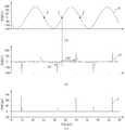
도 1은 종래의 교류 전원의 사인파를 도시한 그래프, 도 2는 도 1의 교류 전원에 의한 엘이디(LED) 조명장치에서 분할 제어를 위한 조명 램프의 회로도이다.FIG. 1 is a graph showing a sine wave of a conventional AC power source, and FIG. 2 is a circuit diagram of an illumination lamp for division control in an LED lighting device by the AC power supply of FIG.
도 1 및 2를 참조하면, 조명램프는 다 수개의 엘이디(D1~D4)가 직렬 연결된다. 예를 들면, 엘이디(LED)는 전류 구동소자로 높은 전압이 인가되면 파손되므로 정격이상의 전류가 입력되면 안된다.Referring to FIGS. 1 and 2, the illumination lamp includes a plurality of LEDs D1 to D4 connected in series. For example, an LED (LED) is a current driving device, which is damaged when a high voltage is applied.
하지만, 교류전원에서 엘이디(LED)를 직접구동하기 위해서는 엘이디(LED)가 높은 전압에서 구동되어야 한다. 즉, 다 수개의 엘이디(LED)를 구비하는 조명램프를 구동시키기 위해서는 AC 220V를 직류(DC)로 정류할 경우에 얻어지는 최대 310V에 이르는 높은 전압을 이용하여 정격 전류를 효율적으로 제어해야 한다.However, in order to drive the LED directly from the AC power source, the LED must be driven at a high voltage. That is, in order to drive an illumination lamp having a plurality of LEDs, the rated current should be efficiently controlled by using a high voltage up to 310 V obtained when rectifying AC 220V to DC.
따라서, 종래에는, 도 1 및 도 2에 도시된 바와 같이, DC 300V를 각 단계로 나누어 조명램프의 엘이디(LED)(D1~D4)를 순차적으로 발광되도록 제어한다.Therefore, conventionally, as shown in FIG. 1 and FIG. 2, DC 300V is divided into respective steps to control the LEDs (D1 to D4) of the illumination lamp to sequentially emit light.
즉, 종래의 조명램프는 교류를 직류화 했을 때 얻어지는 직류 사인파의 위상에 따라 설정된 각 구간별로 직렬로 순차 연결된 제1 내지 제4 엘이디(D1~D4)를 순차적으로 발광시킨다.That is, the conventional illumination lamp sequentially emits the first through fourth LEDs D1 through D4 sequentially connected in series for each section set according to the phase of the DC sine wave obtained when the alternating current is converted into DC.
보다 상세히 설명하자면, 전원부에서 입력된 교류 전원은, 도 1과 같은 제로 크로싱(ZERO CROSSING) 시점부터 60㎐ 간격으로 사인파(SIGN SIGNAL) 곡선을 그리게 된다.More specifically, the AC power input from the power supply unit draws a SIGNAL SIGNAL curve at intervals of 60 Hz from the zero crossing point as shown in FIG.
그래서, 종래에는 사인파의 전압별 위상 구간을 분할하여 제1 내지 제4 엘이디(D1~D4)를 순차적으로 제어한다. 예를 들면, 도 1의 사인파는 위상에 따라 총 1 내지 7구간으로 분할된다. 이중 1과 7구간은 0~70V, 2와 6구간은 71~140V, 3과 5구간은 141~210V, 4구간은 211V 이상의 전압 구간이다.Thus, conventionally, the first to fourth LEDs D1 to D4 are sequentially controlled by dividing the phase interval of each sinusoidal voltage. For example, the sine wave of FIG. 1 is divided into a total of 1 to 7 intervals according to the phase. The first and seventh sections are 0 to 70 V, the second and sixth sections are 71 to 140 V, the third and fifth sections are 141 to 210 V, and the fourth section is a voltage section of 211 V or more.
따라서, 종래의 조명램프는 1구간과 7구간에 설정된 전압일 경우에 제1엘이디(D1)의 입력측에 전원이 출력되어 제1엘이디(D1)가 발광되고, 2와 6구간의 전압이면 제2엘이디(D2)의 입력측에 전원이 출력되어 제2엘이디(D2)와 제1엘이디(D1)가 순차 발광되고, 3과 5 구간의 전압이면 제3엘이디(D3)의 입력측에 전원이 출력되어 제3엘이디(D3) 내지 제1엘이디(D1)가 순차 발광되고, 4구간의 전압이면 제4엘이디(D4)의 입력측에 전원이 출력되어 제4엘이디(D4)부터 제1엘이디(D1)까지 순차 발광 된다.Accordingly, when the voltage of the conventional illumination lamp is a voltage set in the first period and the seventh period, the power is outputted to the input side of the first LED D1 to emit the first LED D1, Power is outputted to the input side of the LED D2 and the second LED D2 and the first LED D1 are sequentially emitted. When the voltage is in the third and fifth intervals, power is outputted to the input side of the third LED D3, The third LED D3 to the first LED D1 are sequentially lighted and if the voltage of the fourth period is a voltage, the power is outputted to the input side of the fourth LED D4 to sequentially turn on the fourth LED D4 to the first LED D1 And is emitted.
즉, 종래의 조명램프는 광량을 높이기 위해서 높은 전압을 출력하여 발광되는 엘이디(LED)의 숫자를 증가시키거나, 광량을 낮추기 위해서는 낮은 전압을 출력하여 발광되는 엘이디(LED) 숫자를 감소시키는 방식으로 디밍 제어가 이루어질 수 있다.That is, in the conventional illumination lamp, in order to increase the light amount, a method of increasing the number of emitted LEDs by outputting a high voltage or decreasing the number of emitted LEDs The dimming control can be performed.
또는, 위와 같은 단순 전압의 높낮이를 통한 디밍제어에 방식에 비하여 정밀한 제어를 위하여 각 전압의 위상구간별로 디밍 제어가 이루어질 수 있다. 즉, 종래에는, 예를 들면, 트라이악을 이용하여 위와 같이 제로크로싱(ZERO CROSSING) 지점을 기준으로 조명램프의 디밍제어가 이루어졌다. 이는 도 3과 도 4를 참조하여 설명한다.Alternatively, the dimming control may be performed for each phase interval of each voltage for precise control in comparison with the dimming control through the height of the simple voltage as described above. That is, conventionally, for example, dimming control of the illumination lamp is performed based on the ZERO CROSSING point using the triac as described above. This will be described with reference to FIG. 3 and FIG.
도 3은 종래의 디밍 제어의 일예를 도시한 그래프, 도 4는 종래의 디밍 제어시에 발생되는 플리커(FLICKER) 현상을 도시한 그래프이다. FIG. 3 is a graph showing an example of a conventional dimming control, and FIG. 4 is a graph showing a flicker phenomenon generated in a conventional dimming control.
도 3을 참조하면, 종래에는 트라이악을 이용한 디밍 제어는 사인파의 제로크로싱(Z)를 기준으로 제어한다(도 3의 (a) 참조). 예를 들면, 조명 램프에서 전체 엘이디(D1~D4)가 발광되었을 경우의 광량을 100%로 설정하고, 80%로서 광량을 조절할 경우에는 제로크로싱(Z)를 기준으로 하여 80%의 위상 구간 동안만 발광제어시킨다(도 3의 (b) 참조). 이 경우에는 도 1의 1 내지 7구간중 2구간에서 7구간 동안에 조명램프가 발광된다. 즉, 1구간에서는 발광되지 않고, 2구간부터 7구간까지 발광된다.Referring to FIG. 3, conventionally, dimming control using a triac controls based on zero crossing (Z) of a sine wave (see FIG. 3 (a)). For example, when the amount of light when all the LEDs D1 to D4 are emitted from the illumination lamp is set to 100% and the amount of light is adjusted to 80%, the light amount is controlled to be 80% of the phase interval (See Fig. 3 (b)). In this case, the illumination lamp is emitted during seven sections from two sections out of the
또는, 50%로 디밍 제어는, 도 3의 (c) 참조, 피크점부터 제로크로싱(Z)까지의 구간 동안만 발광시킨다. 즉, 조명램프는 4구간의 절반부터 7구간까지 엘이디(D1~D4)를 발광시킨다. 이때, 조명램프는 양의 반주기 동안 전체 엘이디(LED)가 전부 점등된 상태에서 제4엘이디(D4)부터 제1엘이디(D1)까지 순차 소등된 이후에 음의 반주기 동안 같은 과정을 반복하게 된다.Alternatively, the dimming control at 50% is performed only during the period from the peak point to the zero crossing (Z) with reference to FIG. 3 (c). That is, the illumination lamp emits the LEDs D1 to D4 from the half of the four sections to the seven sections. At this time, the illumination lamp is sequentially turned off from the fourth LED D4 to the first LED D1 in a state where all of the LEDs are fully turned on during the positive half period, and then the same process is repeated for half the negative period.
또는, 20%의 디밍 제어는, 도 3의 (d) 참조, 제로크로싱(Z)부터 180도의 위상구간중 20%에 해당되는 구간(144~180도) 동안 엘이디(D1)를 발광시킨다.3 (d), the dimming control of 20% causes the LED D1 to emit during a period (144 to 180 degrees) corresponding to 20% of the phase interval of 180 degrees from the zero crossing (Z).
그러나 교류 전압은 현질적으로 고정된 값이 될 수 없다. 이것은 상용 교류 계통에서 다양한 형태의 부하가 형성되어 계통의 전압크기가 부하조건에 따라 10~20% 수준으로 가변적이기 때문이다.However, the AC voltage can not be a fixed value in the present. This is because various types of loads are formed in a commercial AC system, and the voltage magnitude of the system is varied from 10 to 20% depending on the load conditions.
따라서, 상술한 바와 같이 트라이악을 이용한 엘이디 조명램프의 디밍 장치는 디밍의 범위를 결정하는 위상각의 값이 고정되었다고 하여도 변화량에 대응한 출력전압이 일정비로 변화하게 된다. 그러므로 교류 전원에 의해 구동되는 조명램프의 엘이디(LED)에 플리커(FLICKER) 현상을 유발할 수 있다.Therefore, as described above, even when the value of the phase angle that determines the range of dimming is fixed, the output voltage corresponding to the change amount is changed at a constant ratio in the dimming device of the LED illumination lamp using the triac. Therefore, a flicker phenomenon may occur in an LED of an illumination lamp driven by an AC power source.
이는 엘이디(LED)가 발광되기 위해서 설정된 레벨의 순방향 전압이 입력되어야 하나, 외부 환경에 의해 상기와 같은 교류 전압(V1)은 일정비로 변화되기에 임계값 이하의 전압(임계전압)(V2)으로 변화된다. 이와 같은 임계전압의 변화는 주로 전압이 낮은 대역에서 발생된다. 이는 도 4의 그래프를 통하여 확인될 수 있다.This is because the forward voltage of the set level is required for the LED to emit light but the alternating voltage V1 is changed by the external environment at a predetermined ratio and the voltage is lower than the threshold voltage V2 Change. Such a change in the threshold voltage occurs mainly in a low voltage band. This can be confirmed through the graph of FIG.
도 4의 (a)는 교류전압의 사인파(V1)를 도시한 그래프이고, 도 4의 (b)는 엘이디(LED)의 임계 전압의 변화를 측정하는 그래프이고, 도 4의 (c)는 엘이디(LED)의 전류값을 측정한 그래프이다.FIG. 4A is a graph showing a sinusoidal wave V1 of an AC voltage, FIG. 4B is a graph of a change in the threshold voltage of the LED, (LED).
도 1과 도 4의 (a) 내지 (c)를 상호 교차 비교해보면, 임계전압(V2)의 변화는 주로 교류전압이 낮은 대역의 위상구간(예를 들면, 도 1의 1, 2구간과 6, 7구간)에서 발생됨이 확인된다. 이때, 도 4의 (b)와 (c)를 비교해보면, 임계전압(V2)이 변화되는 구간에서 전류(I)가 갑자기 상승했다가 떨어지는 것이 확인된다.1 and 4 (a) to 4 (c), the variation of the threshold voltage V2 mainly depends on the phase interval of the low band (for example, between the first and second sections of FIG. 1 and 6 , 7 intervals). At this time, when comparing (b) and (c) in FIG. 4, it is confirmed that the current I suddenly rises and falls in a section where the threshold voltage V2 changes.
즉, 조명램프(210, 220)의 엘이디(LED)들은 전압이 낮은 대역의 위상 구간(1-2, 6-7)에서 디밍 제어시에 임계전압(V2)의 변화로 인하여 엘이디(LED)에 입력되는 전류(I) 값이 불안정함에 따라 플리커 현상을 유발시킨다.That is, the LEDs of the
그러므로, 종래에는 제로크로싱(Z)를 기준으로 위상제어가 이루어질 수 있으나, 상기와 같은 환경의 변화에 따라서 전압이 낮은 대역에서 임계전압의 변동이 이루어질 수 있어 플리커현상이 발생되고, 정밀한 디밍 제어가 이루어질 수 없는 문제점이 있었다.Therefore, conventionally, the phase control can be performed based on the zero-crossing (Z). However, according to the change of the environment, the threshold voltage can be varied in a low voltage band and flicker phenomenon occurs, There is a problem that can not be achieved.
따라서, 상기와 같은 종래의 문제점을 해결하기 위하여 안출된 것으로, 본 발명의 목적은 엘이디를 이용한 조명램프의 디밍 제어시에 플리커(FLIKER) 현상이 방지될 수 있는 엘이디 조명의 디밍 제어장치를 제공하는 것에 있다.SUMMARY OF THE INVENTION Accordingly, it is an object of the present invention to provide a dimming control apparatus for an LED lighting capable of preventing flicker during dimming control of an illumination lamp using an LED It is on.
본 발명은 상기와 같은 목적을 달성하기 위하여 하기와 같은 실시예를 포함한다.The present invention includes the following embodiments in order to achieve the above object.
본 발명에 따른 엘이디 조명의 디밍 제어장치의 바람직한 실시예는 복 수개의 엘이디(LED)가 구비된 적어도 하나의 조명램프와, 조작스위치를 통하여 입력되는 디밍 명령에 따라 설정된 디밍 범위로 점등된 조명램프의 밝기를 제어하는 제어부재를 포함하고, 제어부재는 교류 전원을 공급하는 교류전원부와, 교류전원부에서 출력된 교류 전압에서 사인파의 제로크로싱(ZERO CROSSING)을 감지하여 제로싱크 신호(ZDS)를 발생시키는 제로싱크 발생부와, 사인파의 피크점(PEAK)을 기준으로 위상구간(TA)이 확장될수록 광의 세기가 높아지도록 광의 세기에 대비되도록 위상구간(TA)을 설정하고, 제로싱크 신호(ZDS)들의 시간차를 통하여 사인파의 피크점(PEAK)을 확인하여 피크점(PEAK)을 중심으로 디밍 명령에 일치되는 위상구간(TA)에서 디밍제어신호(DCS)를 출력하는 제어부와, 교류전원부에서 공급된 교류 전원을 정류하여 조명램프로 공급하는 정류부와, 디밍제어신호(DCS)에 따라서 정류부를 온오프시켜 조명램프에 출력되는 직류의 펄스폭을 제어하는 펄스구동부 및 조명램프에 출력되는 교류 전원의 변동유무를 실시간으로 감지하여 제어부에 실시간 모니터링신호를 출력하는 모니터링부를 포함하고, 제어부는 모니터링부의 모니터링 신호를 수신하여 전원의 변동이 감지되면 펄스구동부를 제어하여 전원의 변동이 감지된 구간에서 펄스폭을 증감시키는 엘이디 조명의 디밍 제어장치를 제공할 수 있다.A preferred embodiment of the dimming control apparatus for an LED illumination according to the present invention comprises at least one illumination lamp provided with a plurality of LEDs and an illumination lamp which is illuminated in a dimming range set according to a dimming command inputted through the operation switch And a control member for controlling the brightness of the sine wave. The control member includes an AC power supply for supplying an AC power source and a control unit for generating a zero sync signal (ZDS) by detecting zero crossing of a sine wave from an AC voltage output from the AC power supply And a phase interval TA is set so that the intensity of the light increases as the phase interval TA is expanded based on the peak point PEAK of the sine wave. (PEAK) of the sine wave through the time difference between the peak point (PEAK) and the phase of the sine wave (PEAK) and outputting the dimming control signal (DCS) A pulse driving unit for rectifying the AC power supplied from the AC power supply unit and supplying the rectified AC power to the illumination lamp, a pulse driving unit for controlling the pulse width of DC outputted to the illumination lamp by turning on and off the rectifying unit in accordance with the dimming control signal DCS, And a monitoring unit that detects in real time whether there is a change in AC power output to the lamp and outputs a real-time monitoring signal to the control unit. The control unit receives the monitoring signal of the monitoring unit and controls the pulse driving unit It is possible to provide a dimming control device of an LED illumination which increases or decreases the pulse width in the sensed section.
그러므로, 본 발명은 교류 사인파에서 전압이 높은 위상 구간에서 조명램프에 인가되는 펄스를 제어함에 따라 플리커 현상이 방지되는 효과가 있다.Therefore, the present invention has the effect of preventing the flicker phenomenon by controlling the pulse applied to the illumination lamp in the high phase interval of the AC sine wave.
도 1은 위상구간이 분할된 사인파를 도시한 그래프이다.
도 2는 도 1의 교류 전원에 의한 엘이디(LED) 조명장치에서 분할 제어를 위한 조명 램프의 회로도이다.
도 3은 종래의 트라이악을 이용한 디밍제어의 예를 도시한 그래프이다.
도 4는 종래의 트라이악을 이용한 디밍제어시에 플리커 현상을 측정한 그래프이다.
도 5는 본 발명에 따른 엘이디(LED) 조명의 디밍 제어장치를 도시한 블럭도이다.
도 6은 본 발명의 제어부재를 도시한 블럭도이다.
도 7은 본 발명에서 제로크로싱 및 제로싱크 신호의 예를 도시한 그래프이다.
도 8은 본 발명에서 위상 제어의 일예를 도시한 그래프이다.
도 9는 본 발명에서 정류부를 도시한 도면이다.
도 10은 본 발명에서 광량감지부재를 도시한 블럭도이다.
도 11은 본 발명에서 모니터링의 실시예를 설명하기 위한 블럭도이다.
도 12는 본 발명의 엘이디(LED) 조명의 디밍 제어방법을 도시한 순서도이다.
도 13은 본 발명의 엘이디(LED) 조명의 디밍 제어방법에서 S150 단계를 상세 도시한 순서도이다.
도 14는 본 발명의 엘이디(LED) 조명의 디밍 제어방법에서 S160 단계를 상세 도시한 순서도이다.1 is a graph showing a sine wave in which a phase interval is divided.
FIG. 2 is a circuit diagram of an illumination lamp for division control in an LED lighting device by the AC power supply of FIG. 1; FIG.
3 is a graph showing an example of dimming control using a conventional triac.
FIG. 4 is a graph showing a flicker phenomenon during dimming control using a conventional triac.
5 is a block diagram showing a dimming control apparatus of an LED illumination according to the present invention.
6 is a block diagram showing the control member of the present invention.
7 is a graph showing an example of a zero crossing and a zero sync signal in the present invention.
8 is a graph showing an example of phase control in the present invention.
9 is a view showing a rectifying section in the present invention.
10 is a block diagram showing a light amount sensing member in the present invention.
11 is a block diagram for explaining an embodiment of monitoring in the present invention.
12 is a flowchart showing a dimming control method of the LED illumination of the present invention.
13 is a flowchart showing details of step S150 in the dimming control method of the LED illumination of the present invention.
14 is a flowchart showing details of step S160 in the dimming control method of the LED lighting of the present invention.
이하, 본원이 속하는 기술 분야에서 통상의 지식을 가진 자가 용이하게 실시할 수 있도록 본 발명의 구현 예 및 실시 예를 들어 상세히 설명한다. 그러나 본원은 여러 가지 상이한 형태로 구현될 수 있으며 여기에서 설명하는 구현 예 및 실시 예에 한정되지 않는다.Hereinafter, embodiments and examples of the present invention will be described in detail so that those skilled in the art can easily carry out the present invention. It should be understood, however, that the present invention may be embodied in many different forms and is not limited to the embodiments and examples described herein.
명세서 전체에서, 어떤 부분이 어떤 구성요소를 "포함"한다고 할 때, 이는 특별히 반대되는 기재가 없는 한 다른 구성요소를 제외하는 것이 아니라 다른 구성요소를 더 포함할 수 있는 것을 의미한다. 또한, 명세서에 기재된 "..부", "..부재", "..수단"의 용어는 적어도 하나의 기능이나 동작을 처리하는 구성의 단위를 의미하며, 하드웨어 및/또는 소프트웨어의 결합으로 구현될 수 있다.Throughout the specification, when an element is referred to as "comprising ", it means that it can include other elements as well, without excluding other elements unless specifically stated otherwise. Also, the terms " part, " " absent, "and " means" in the specification mean units of a configuration for processing at least one function or operation and may be implemented by a combination of hardware and / .
도 5는 본 발명에 따른 엘이디(LED) 조명의 디밍 제어장치를 도시한 블럭도, 도 6은 본 발명의 제어부재를 도시한 블럭도, 도 10은 광량감지부재를 도시한 블럭도이다.FIG. 5 is a block diagram showing a dimming control apparatus of an LED illumination according to the present invention, FIG. 6 is a block diagram showing a control member of the present invention, and FIG. 10 is a block diagram showing a light amount sensing member.
도 5 및 도 6을 참조하면, 엘이디(LED) 조명의 디밍 제어장치는 다 수개의 엘이디(LED)가 그룹화된 복 수개의 발광그룹(210, 220)이 직렬 또는 병렬로 연결되는 조명부재(200)와, 조명부재(200)의 온오프 및 디밍을 제어하는 제어부재(100)와, 조명부재(200)의 고장을 감지하는 광량감지부재(300)를 포함한다.5 and 6, a dimming control apparatus for an LED illumination includes a plurality of light emitting
조명부재(200)는 상호간에 직렬로 연결되는 복 수개 이상의 엘이디(LED)가 그룹화된 복 수개의 발광그룹(210, 220)을 포함한다. 여기서 발광그룹(210, 220)은 하나의 조명램프(210, 220)에 해당될 수 있다. 또한 각 발광그룹은 상호 직렬 연결될 수 있다. 이하에서는 조명램프와 발광그룹에 동일한 도면 번호를 부여하여 설명한다.The
제어부재(100)는 복수개의 조명램프(210, 220)를 온오프 및 디밍을 제어한다. 이를 위한 구체적인 구성은 도 6 및 도 10을 참조하여 설명한다.The
도 6 및 도 10을 참조하면, 본 발명에서 제어부재(100)는 디밍 구간을 표시하는 디스플레이(142)와, 디밍 구간을 설정하는 조작스위치(141)와, 경보를 발령하는 경보부(143)와, 교류전원을 출력하는 교류전원부(110)와, 교류전원부(110)와 내부 계통을 절연시키는 트랜스 절연부(120)와, 트랜스 절연부(120)로부터 입력되는 교류 전원에서 제로크로싱(Z)를 감지하는 제로싱크 발생부(130)와, 제로크로싱(Z)를 통하여 교류 전원의 사인파에서 피크점(P)을 산출하여 디밍을 제어하는 제어부(140)와, 노이즈 및 이상전원을 필터링 하는 필터부(150)와, 교류전원을 직류로 변환시키는 정류부(170)를 포함한다.6 and 10, in the present invention, the
여기서, 제로싱크 발생부(130)와 제어부(140)는 절연 트랜스(도시되지 않음)에 의해 절연될 수 있다. 또한, 본 발명은 필터부(150)외에 제어부(140)와 펄스구동부(160) 사이에 절연 트랜스(도시되지 않음)가 추가될 수 있다. 이와 같은 절연 트랜스는 외부의 환경에 따른 영향으로 교류 전원에서 발생되는 노이즈를 미연에 방지하기 위함이다.Here, the zero-
교류전원부(110)는 외부 계통 전원으로서, 예를 들면, 건물 내에 설치된 분전함등에 해당 될 수 있다.The AC
트랜스 절연부(120)는 교류전원부(110)와 내부계통(예를 들면, 건물 내의 각 부하로 연결되는 전원선) 사이를 전기적으로 절연시킨다. 예를 들면, 트랜스 절연부(120)는 교류 전원을 받는 1차측과, 내부 계통에 연결되는 2차측을 구비하고, 1차측과 2차측은 상호 절연된다.The
제로싱크 발생부(130)는 트랜스 절연부(120)의 2차측에서 내부계통으로 출력되는 교류 전원에서 제로크로싱(Z)을 감지하여 제로싱크 신호(ZDS)를 발생한다. 제로싱크 신호(ZDS)는 제어부(140)에 출력된다. 여기서 제로싱크 신호(ZDS)는 도 7의 그래프를 참조하여 설명한다.The zero-
도 7은 제로크로싱(Z) 및 제로싱크 신호(ZDS)의 일예를 도시한 그래프이다.7 is a graph showing an example of a zero crossing (Z) and a zero sync signal (ZDS).
도 7을 참조하면, 제로크로싱(Z)은 (a)에 도시된 사인파의 위상이 0도가 되는 위치를 의미한다. 따라서, 제로싱크 발생부(130)는 트랜스 절연부(120)에서 출력되는 교류 전원에서 (b)에 도시된 바와 같이 제로크로싱(Z)이 감지되면, 제로싱크 신호(ZDS)를 제어부(140)에 순차 출력한다.Referring to FIG. 7, the zero crossing (Z) means a position where the phase of the sine wave shown in (a) is 0 degrees. Therefore, when the zero crossing Z is sensed as shown in (b) in the AC power supply output from the
필터부(150)는 제어부(140)의 구동제어신호에 포함된 노이즈와, 트랜스 절연부(120)의 이상전압(예를 들면, 낙뢰에 의한 서지전압)을 감지하여 필터링 및 차단한다.The
펄스구동부(160)는 디밍제어신호(DCS)가 입력되는 베이스와, 정류부(170)의 출력측에 연결되는 입력단자와, 접지단과 정류뷰의 입력측에 연결되는 출력단자로 구성된 스위칭 소자(Q1)로 구성된다.The
이때, 트랜스 절연부(120)에서 연장되는 양의 전원라인은 정류부(170)의 입력측(제1단자)와 조명램프(210, 220)의 입력측에 각각 연결되고, 음의 전원라인은 스위칭소자(Q1)의 출력단자와 연결되어 정류부(170)의 입력측(제2단자)에 연결된다.At this time, a positive power supply line extending from the
제어부(140)는 제로싱크 신호(ZDS)가 수신되면, 제로크로싱(Z)를 기준으로 반주기의 시간을 연산하여 피크점(P)을 산출한다. 예를 들면, 제어부(140)는 60Hz의 사인파에서 제로싱크 신호가 순차적으로 수신되는 시간주기를 측정한다. 따라서, 60Hz의 사인파의 한주기가 16.7msec로 확인되면, 반주기가 8.35msec 임에 따라 이를 다시 0.5를 곱하여 4.175msec의 피크점(P)을 산출한다.When the zero sync signal ZDS is received, the
그리고 제어부(140)는 피크점(P)을 기준으로 광의 세기에 비례하도록 설정된 위상 구간(TA)을 산출하여 펄스구동부(160)에 디밍제어신호(DCS)를 출력한다. 여기서, 교류 전압은 사인파의 피크점(P)에 가까울수록 전압이 높다.The
따라서, 제어부(140)는 전압이 가장 높은, 예를 들면, 사인파의 피크점(PEAK)(P)부터 조명램프의 디밍제어를 개시한다. 그러므로, 디밍 제어신호(DCS)는 조명램프(210, 220)는 사인파의 피크점(P)을 기준으로 양측의 위상 구간(TA)이 넓어질수록 조명 램프에서 출력된 광의 세기가 높아지도록 설정된다.Therefore, the
즉, 조명램프(210, 220)는 사인파의 피크점(P)을 기준으로 확장된 위상 구간(TA)이 커질수록 광의 세기가 높아지고, 좁을수록 광의 세기가 낮아지도록 조명램프(210, 220)에 공급되는 직류의 펄스폭을 제어하여 디밍을 제어한다.That is, the
또한, 제어부(140)는 사인파(SINE WAVE)의 피크점(P)을 기준으로 하여 확장되는 위상 구간(TA) 별로 조명램프(210, 220)에 출력되는 펄스폭이 설정된다.The
따라서, 제어부(140)는 조작스위치(141)를 통하여 입력된 디밍 명령에 따라 설정된 위상 구간을 포함하는 디밍제어신호(DCS)를 펄스구동부(160)에 출력하여 정류된 전원의 펄스폭을 설정된 레벨로 변조하여 조명 램프를 발광시킨다. 구체적인 실시예는 펄스구동부(160)의 설명과 함께 후술한다.Accordingly, the
펄스구동부(160)는 교류 전원에서 양의 반주기 구간에서 디밍제어신호(DCS)가 베이스에 입력되면 턴온되어 정류부(170)의 출력측과 접지단(GND)을 통전시킨다. 또는 펄스구동부(160)는 교류 전원에서 음의 반주기 구간에서 디밍제어신호(DCS)가 인가되면 오프된다.The
그러므로, 펄스구동부(160)는 디밍제어신호(DCS)에 따라 상기 정류부(170)를 구동시켜 설정된 펄스가 상기 조명램프(210, 220)에 출력하도록 한다. 이때, 디밍제어신호(DCS)는 조작스위치(141)에서 입력된 디밍 범위에 따라 피크점(P)을 중심으로 하여 보다 확장 또는 축소된 위상 구간(TA) 별로 펄스구동부(160)의 펄스 제어가 차별되도록 한다.Therefore, the
보다 구체적으로 설명하자면, 제어부(140)는 조작스위치(141)를 통하여 엘이디(LED)들의 전체 광량에서 5%만 출력되도록 디밍 명령이 입력되면, 도 8의 (a)에 도시된 바와 같이 사인파의 피크점(P)을 기준으로 전체 면적의 5%에 해당되는 위상 구간으로 설정된 디밍제어신호(DCS)를 펄스구동부(160)에 출력한다. 따라서, 펄스구동부(160)는 해당 위상 구간(TA)으로 설정된 레벨의 펄스가 출력되도록 정류부(170)를 구동시킨다.More specifically, when the dimming command is input so that only 5% of the total light amount of the LEDs is output through the
또는, 제어부(140)는 조작스위치(141)를 통하여 도 8의 (b)에 도시된 바와 같이 전체 광량의 10%만 출력시키도록 디밍 명령이 입력되면, 사인파의 반주기 전체 구간에서 피크점(P)을 기준으로 10%의 위상 구간(TA)에 대비된 디밍제어신호(DCS)를 펄스구동부(160)에 출력한다. 그러므로 펄스구동부(160)는 디밍제어신호(DCS)에 따라 설정된 펄스가 출력되도록 정류부(170)를 펄스폭변조(PWM) 제어한다.Alternatively, when the dimming command is inputted through the
또는, 제어부(140)는 조작스위치(141)를 통하여, 도 8의 (c)에 도시된 같이, 전체 광량의 90%에 해당되는 광량을 출력시키도록 디밍 명령이 입력되면, 사인파의 반주기 구간중 피크점(P)을 기준으로 90%의 해당되는 위상 구간(TA)에 대비된 디밍제어신호(DCS)를 펄스구동부(160)에 출력한다. 따라서, 펄스구동부(160)는 디밍제어신호(DCS)에 따라 펄스폭을 변조하여 정류부(170)를 구동시킨다.Alternatively, when a dimming command is input through the
따라서, 본 발명의 각 엘이디(LED)들의 광량은 피크점을 기준으로 양측으로 확장된 위상 구간(TA)에서 펄스구동부(160)의 펄스폭변조(PWM) 제어가 이루어짐에 따라 전압이 높은 대역에서 가장 낮은 광의 세기가 출력되는 디밍 범위의 제어가 이루어질 수 있다.Therefore, as the light intensity of each LED of the present invention is controlled by the pulse width modulation (PWM) of the
정류부(170)는 펄스구동부(160)의 온오프에 따라 트랜스 절연부(120)로부터 출력된 교류 전압을 직류화하여 조명부재(200)로 출력한다. 여기서 정류부(170)는 브릿지 다이오드로 구비될 수 있다.The
그러나, AC 조명램프(210, 220)를 발광시키기 위하여 전원이 출력되면, 정류 다이오드로 이루어진 브릿지 다이오드에 직접적인 부하가 걸리는 것이 아닌 정류부를 스위칭하기 위한 스위치부의 스위칭소자(Q1)과, 브릿지 다이오드(D2)에 부하가 걸린다. 그중에서 스위칭소자(Q1)은, 예를 들면, 트랜지스터일 경우에 턴온(Turn on) 저항이 낮아 전력손실이 적지만, 브릿지 다이오드(D2)는 순방향 전압에 의한 손실이 커서 발열량이 많은 문제가 있다.However, when power is outputted to cause the
예를 들면, 브릿지 다이오드 1개의 순방향 전압은 1.1V이기에 2개의 순방향전압은 2.2V 이다. 따라서, 전류 20A의 AC 전원이 입력되면, 정류부에서 44W의 손실전력이 발생된다.For example, the forward voltage of a bridge diode is 1.1V, and the two forward voltages are 2.2V. Therefore, when AC power of 20 A is inputted, 44 W of loss power is generated in the rectifying part.
즉, AC 조명램프(210, 220)에서 브릿지 다이오드를 사용할 경우에, 발열온도가 높아 열을 외부로 전도시키는 방열판의 사이즈를 키워야 되는 문제가 있다.That is, when the bridge diodes are used in the
따라서, 본 발명은 이와 같은 방열판의 확장을 방지하고자 턴온 저항이 낮은 스위칭소자(예를 들면, FET)를 적용하여 전력손실 및 발열량을 줄일 수 있도록 하였다. 이는 도 9에 도시된 바를 참조하여 설명한다.Therefore, in order to prevent the heat spreader from expanding, the present invention can reduce power loss and heat generation by applying a switching element (for example, FET) having a low turn-on resistance. This will be described with reference to FIG.
도 9는 본 발명의 정류부를 도시한 도면이다.9 is a view showing a rectifying part of the present invention.
도 9를 참조하면, 정류부(170)는 트랜스 절연부(120)에서 입력되는 음의 반주기와 양의 반주기 신호를 각각 도통시키는 제1 내지 제4 스위칭수단(SW1~SW4)과, 제1 내지 제4스위칭수단(SW1~SW4)을 온오프시키는 정류제어수단(171)을 포함한다.9, the rectifying
여기서, 제1 내지 제4스위칭수단(SW1~SW4)은 턴온(Turn on) 저항이 낮은 FET가 일예로 적용되었다.Here, the first through fourth switching means SW1 through SW4 have been applied to FETs having a low turn-on resistance.
여기서, 제1스위칭수단(SW1)은 정류제어수단(171)의 TG1 단자에 베이스가 연결되고, 입력단이 정류부(170)의 제1단자, 출력단자가 정류부(170)의 제4단자에 연결된다.The first switching means SW1 has its base connected to the TG1 terminal of the rectifying control means 171 and has its input terminal connected to the first terminal of the rectifying
제2스위칭수단(SW2)은 베이스가 정류제어수단(171)의 TG2단자에 연결되고, 입력단자가 정류부(170)의 제2단자, 출력단자가 정류부(170)의 제1단자에 연결된다.The second switching means SW2 has its base connected to the TG2 terminal of the rectification control means 171 and its input terminal connected to the second terminal of the
제3스위칭수단(SW3)은 베이스가 정류제어수단(171)은 BG1단자에 연결되고, 입력단자가 정류부(170)의 제2단자, 출력단자가 정류부(170)의 제3단자에 연결된다.The third switching means SW3 has a base connected to the BG1 terminal of the rectifying control means 171 and has an input terminal connected to the second terminal of the rectifying
제4스위칭수단(SW4)은 베이스가 정류제어수단(171)의 BG2단자에 연결되고, 입력단자가 정류부(170)의 제3단자에 연결되고, 출력단자가 정류부(170)의 제4단자에 연결된다.The fourth switching means SW4 has a base connected to the BG2 terminal of the rectification control means 171, an input terminal connected to the third terminal of the
정류제어수단(171)은 제어부(140)의 제어에 따라서, 트랜스 절연부(120)로부터 출력되는 전원에서 제1스위칭수단(SW1)과 제3스위칭수단(SW3)을 턴온시켜 양(+)의 반주기를 정류하고, 제2스위칭수단(SW2)과 제4스위칭수단(SW4)을 턴온시켜 음(-)의 반주기를 정류한다.The rectification control means 171 turns on the first switching means SW1 and the third switching means SW3 in the power supply outputted from the
이때, 제1스위칭수단(SW1)과 제3스위칭수단(SW3)은 정류제어수단(171)의 제어에 의하여 턴온됨에 따라 트랜스 절연부(120)와 엘이디(LED)간의 회로를 도통시킨다. 여기서 제2스위칭수단(SW2)과 제4스위칭수단(SW4)은 턴오프된다.At this time, the first switching means SW1 and the third switching means SW3 are turned on under the control of the rectification control means 171, so that the circuit between the
또한, 제2스위칭수단(SW2)과 제4스위칭수단(SW4)은 정류제어수단(171)의 제어에 의하여 턴온되면서 트랜스 절연부(120)와 엘이디(LED)간의 회로를 도통시킨다. 여기서 제1스위칭수단(SW1)과 제3스위칭수단(SW3)은 턴오프된다.The second switching means SW2 and the fourth switching means SW4 are turned on under the control of the rectification control means 171 to turn on the circuit between the
그러므로, 본 발명은 턴온(Turn on) 저항이 낮은 스위칭소자로서 정류부를 구성함에 따라 발열량을 줄일 수 있어 방열판의 면적을 줄일 수 있다. 이와 같은 방열판의 축소는 외관 케이스를 소형화 할 수 있어 제조원가의 절감을 통한 제품 경쟁력을 올릴 수 있도록 해준다.Therefore, according to the present invention, since the rectifying part is constituted as a switching device having a low turn-on resistance, the amount of heat generated can be reduced, and the area of the heat sink can be reduced. Reducing the size of the heat sink makes it possible to reduce the size of the outer case, thereby reducing the manufacturing cost and increasing the product competitiveness.
광량감지부재(300)는 조명부재(200)에서 출력되는 광량을 감지하여 제어부재(100)에 고장감지 여부를 출력한다. 보다 상세한 설명은 도 10을 참조하여 설명한다.The light
도 10은 본 발명에서 광량감지부재를 도시한 블럭도이다.10 is a block diagram showing a light amount sensing member in the present invention.
도 10을 참조하면, 광량감지부재(300)는 조명부재(200)의 광량을 감지하는 광센서(310)와, 외란광에 의한 광센서(310)의 출력을 조절하는 자동이득조절부(320)와, 광센서(310)의 출력신호에 포함된 노이즈를 제거하는 노이즈 제거부(330)부를 포함한다.10, the light
광센서(310)는 예를 들면, 포토다이오드로서 조명부재(200)의 램프별 또는 복수개의 램프로 이루어진 그룹별로 설치되어 광량을 감지한다.The
자동이득조절부(320)는 광센서(310)가 주변의 외란광에 의하여 실제 조명램프(210, 220)의 발광된 광량에 비하여 높은 레벨의 신호가 출력되는 것을 방지하고자 광센서(310)에서 출력신호의 이득(GAIN)을 자동으로 조절하여 외란광에 의한 노이즈가 차감되어 실제 조명램프(210, 220)에서 감지된 신호만을 출력하도록 한다.The automatic
노이즈 제거부(330)는 광센서(310)의 광감지신호(PDS)에 포함된 노이즈를 제거하여 비교부(340)로 출력한다. 이를 위하여 노이즈 제거부(330)는 하이패스 필터 및 로우패스 필터를 구비하여 설정된 대역을 제외한 대역의 신호를 제거한다.The
제어부(140)는 상기와 같은 광량감지부재(300)의 광량 감지신호를 수신하여 조명램프(210, 220)의 고장여부를 감지할 수 있다. 여기서, 제어부(140)는 외란광 및 기타 주변 환경에 의한 오차범위를 줄이기 위하여 사인파의 위상 구간별로 측정된 광량과, 제로크로스(Z)에서 측정된 광량을 연산하여 실제 광량을 연산한다.The
그리고, 제어부(140)는 연산된 실제 광량과 설정된 기준값을 비교하여 조명램프(210, 220)의 고장여부를 판단한다.Then, the
또한, 본 발명은 조명램프(210, 220)의 디밍 제어시에 교류 입력전원(AC)의 변동에 따라 조명램프(210, 220)의 플리커 현상을 방지하기 위하여 입력전원을 상시 모니터링 하는 것이 바람직하다.It is preferable that the input power is continuously monitored in order to prevent the flickering of the
예를 들면, 교류 입력전원(AC)에 의해 구동되는 엘이디 조명램프(210, 220)는 아주 적은 전기 소비로 밝은 빛을 내기 위하여 아주 작은 입력전원의 변화에도 광량의 변화가 발생된다. 특히, 교류 엘이디 조명램프(210, 220)의 디밍 제어시에는 낮은 밝기로 디밍 범위가 설정되었을 경우에 전압변동이 많아진다.For example, the
즉, 예를 들면, AC 60Hz의 사인파가 공급되는 엘이디 조명램프(210, 220)는 1초에 2번 점등한다. 이때, 사인파의 한주기에서 100us의 시간동안 점등되는 것으로 제어가 이루어질 때, 외부 교류 입력이 변동되면 사람 눈에 깜박이는 현상을 느낄 수 있다.That is, for example, the
따라서, 본 발명은 도 11의 모니터링부(180)를 구비하여 교류 입력전원(AC)에서 전원이 발생된 구간을 검출하여 이에 대응되도록 펄스폭을 조절하여 상술한 바와 같은 플리커 현상을 방지할 수 있도록 한다. 이하에서는 도 11을 참조하여 설명한다.Accordingly, the present invention can be applied to the
도 11은 본 발명의 모니터링부가 구비된 블럭도이다.11 is a block diagram of a monitoring unit according to the present invention.
도 11을 참조하면, 본 발명은 트랜스 절연부를 통하여 조명램프(210, 220)로 입력되는 입력 교류전원을 상시 모니터링 하는 모니터링부(180)를 포함한다.Referring to FIG. 11, the present invention includes a
모니터링부(180)는 교류 입력전원(AC)의 사인파에서 각 위상구간별 전압 및/또는 전류의 변동 여부를 상시 모니터링 하여 그 결과를 제어부(140)에 출력한다. 여기서, 모니터링부(180)는, 예를 들면, 홀센서로서 교류 입력전원(AC)의 전류의 변동을 감지하여 전압으로 변환시켜 출력한다. 또는, 모니터링부(180)는 위와 같은 교류 입력전원(AC)에서 전압을 감지하여 변동 여부를 감지함도 가능하다. 이는 일반적으로 공지된 구성임에 따라 설명을 생략한다.The
즉, 모니터링부(180)는 교류 입력전원(AC)의 위상구간별 전류 변동을 감지하여 제어부(140)에 모니터링 감지신호(IDS)를 출력한다.That is, the
이때, 제어부(140)는 제로싱크 발생부(130)로부터 출력된 제로싱크 신호를 통하여 사인파의 각 위상구간을 연산하여 모니터링부(180)에서 감지된 전류가 변동된 위상구간을 산출한다. 그리고, 제어부(140)는 펄스구동부를 제어하여 해당 위상구간에서의 디밍제어시에 펄스폭을 보다 증가 또는 감소시켜 조명램프(210, 220)에서 밝기가 일정하도록 한다.At this time, the
본 발명은 상기와 같은 구성을 포함하며, 이하에서는 도 12의 순서도를 참조하여 엘이디(LED) 조명의 디밍 제어방법을 설명한다.The present invention includes the above-described configuration. Hereinafter, a dimming control method of an LED illumination will be described with reference to the flowchart of FIG.
도 12는 본 발명에 따른 엘이디(LED) 조명의 디밍 제어방법을 도시한 순서도이다.12 is a flowchart showing a dimming control method of an LED illumination according to the present invention.
도 12를 참조하면, 본 발명의 엘이디(LED) 조명의 디밍 제어방법은 디밍명령을 수신하는 S110 단계와, 교류전원의 제로크로싱(Z)를 감지하는 S120 단계와, 사인파의 피크점(P)을 연산하는 S130 단계와, 피크점(P)을 기준으로 디밍 범위별로 설정된 위상 구간(TA)을 연산하는 S140 단계와, 피크점(P)을 기준으로 연산된 위상 구간(TA)별로 설정된 디밍제어신호(DCS)로 펄스구동부(160)를 제어하는 S150 단계와, 고장감지신호(EDS)가 수신되는 지를 판단하는 S160 단계와, 고장감지신호(EDS)가 수신되면 경보를 발령하는 S160 단계를 포함한다.Referring to FIG. 12, the dimming control method of an LED illumination according to the present invention includes a step S110 of receiving a dimming command, a step S120 of detecting a zero crossing Z of an AC power source, a step S120 of detecting a peak point P of a sine wave, Calculating a phase interval TA for each dimming range based on the peak point P and calculating a phase interval TA for each phase interval TA calculated based on the peak point P, S160 of controlling the
S110 단계는 제어부(140)가 조작스위치(141)를 통하여 입력되는 디밍 명령을 수신하는 단계이다. 여기서, 사용자는 제어부재(100)에 설치된 광량의 업(UP) 또는 다운(DOWN) 명령이 설정된 조작스위치(141)중 어느 하나를 조작하여 디밍 범위(조명의 세기)를 설정한다. 따라서, 제어부(140)는 조작스위치(141)로부터 입력되는 디밍 명령(광의 세기를 업(UP) 또는 다운(DOWN))을 수신한다.Step S110 is a step in which the
S120 단계는 제어부(140)가 제로싱크 신호(ZDS)를 수신하는 단계이다. 제로싱크 발생부(130)는 트랜스 절연부(120)를 통하여 출력되는 교류전원에서 제로크로싱(Z)을 감지한다. 그리고 제로싱크 발생부(130)는 제어부(140)에 제로싱크 신호(ZDS)를 송신한다.In step S120, the
S130 단계는 제어부(140)가 제로싱크 신호(ZDS)를 통하여 사인파의 피크점(P)을 연산하는 단계이다. 이때, 제어부(140)는 제로크로싱(Z)에서 다음 제로크로싱(Z)까지의 시간을 통하여 반주기를 연산하고, 반주기의 중심점을 피크점(P)으로 산출한다.In step S130, the
S140 단계는 제어부(140)가 S110 단계에서 수신된 디밍 명령에 포함된 광의 세기로 조명부재(200)를 제어하기 위한 위상 구간(TA)을 산출하는 단계이다. 위상 구간(TA)은 광의 세기가 높아질수록 피크점을 중심으로 확장된다.In step S140, the
그러므로 제어부(140)는 디밍 명령에 일치되는 광의 세기에 대비되는 위상 구간(TA)을 S130 단계에서 연산된 피크점(P)을 중심으로 확장되는 구간별로 설정한다. 여기서, 광의 세기별 위상 구간(TA)은 미리 설정되거나, 별도의 알고리즘에 의하여 연산될 수 있다.Therefore, the
S150 단계는 제어부(140)가 피크점(P)을 중심으로 연산된 위상 구간(TA)에서 펄스구동부(160)를 제어하는 단계이다.Step S150 is a step in which the
예를 들면, 사용자가 조작스위치(141)를 통하여 디밍 제어가 전체 광량에서 30% 밝기로 광의 출력이 이루어지도록 디밍 명령을 입력한다. 따라서, 제어부(140)는 제로크로싱(Z)들간의 시간차를 통하여 반주기를 연산하고, 반주기의 중심점으로 피크점(P)을 설정한다. 그리고 제어부(140)는 S140 단계에서 연산된 위상 구간(TA)을 피크점(P)을 중심으로 양측으로 확장하여 설정한다.For example, the user inputs a dimming command through the
이후, 제어부(140)는 설정된 위상 구간(TA)에 따라 설정된 펄스가 출력되도록 펄스구동부(160)에 디밍제어신호(DCS)를 출력한다.The
따라서, 펄스구동부(160)는 디밍제어신호(DCS)에 따라서 설정된 펄스폭으로 변조된 직류가 조명램프(210, 220)에 공급되도록 정류부(170)를 구동시킨다. 이때, 정류부(170)는 정류제어수단(171)에서 펄스구동부(160)의 온오프와 연동되어 TG1과 TG2, BG1, BG2 단자를 선택적으로 온오프시켜 트랜스 절연부(120)에서 출력되는 교류전원을 정류하여 조명부재(200)로 출력한다.Accordingly, the
여기서, 본 발명은 교류 입력전원(AC)을 상시 모니터링하여 전원의 변동이 발생된 구간별로 펄스폭을 제어함을 특징으로 한다. 이는 도 13을 참조하여 후술한다.Here, the present invention is characterized in that the pulse width is controlled by intervals of the power source by monitoring the AC input power source (AC) at all times. This will be described later with reference to FIG.
S160 단계는 제어부(140)에서 광량감지부재(300)에서 수신된 광량을 통하여 조명램프(210, 220)의 고장여부를 판단하는 단계이다. 이와 같은 S160 단계의 상세한 설명은 하기의 도 14를 참조하여 후술한다.In step S160, the
S170 단계는 제어부(140)가 광량감지부재(300)로부터 고장감지신호(EDS)가 수신되면, 제어부재(100)의 디스플레이(142)를 통한 문자나 발광표시 또는 경보부(143)를 구동시켜 청각적 경보를 발령할 수 있다.The
그러므로 본 발명은 교류 전원에서 전압이 가장 높은 대역인 사인파의 피크점(P)부터 광의 세기가 낮은 디밍 제어(전체 광량의 20%미만)가 이루어짐에 따라 종래와 같은 플리커 현상이 방지될 수 있다.Therefore, according to the present invention, since the dimming control (less than 20% of the total amount of light) is performed from the peak point P of the sine wave having the highest voltage in the AC power source to the intensity of light, flicker phenomenon as in the conventional art can be prevented.
도 13은 본 발명의 엘이디(LED) 조명의 디밍 제어방법에서 S150 단계를 상세 도시한 순서도이다.13 is a flowchart showing details of step S150 in the dimming control method of the LED illumination of the present invention.
도 13을 참조하면, S150 단계는 교류 입력전원(AC)을 상시 모니터링하는 S151 단계와, 전류 및/또는 전압의 변동을 감지하는 S152 단계와, 전류 및/또는 전압 변동이 발생된 구간의 펄스폭을 제어하는 S153 단계를 포함한다.Referring to FIG. 13, step S150 includes steps S151, S152, and S152 of monitoring the AC input power source AC at all times, detecting a variation in current and / or voltage, In step S153.
S151 단계는 제어부(140)가 모니터링부(180)의 상시 모니터링 신호(IDS)를 수신하는 단계이다. 예를 들면, 모니터링부(180)는 홀센서로서 트랜스 절연부(120)와 조명램프(210, 220)간 전원라인에서 공급되는 교류 입력전원(AC)의 변동유무를감지한다. The step S151 is a step in which the
S152 단계는 제어부(140)는 모니터링부(180)의 모니터링신호와, 제로싱크 신호(ZDS)를 비교하여 전원의 변동이 발생된 구간을 확인하는 단계이다. 제어부(140)는 설정된 기준값과 모니터링부(180)의 모니터링 신호의 레벨을 비교하여 변동유무를 판단하고, 제로싱크 발생부(130)의 제로싱크 신호(ZDS)와 모니터링부(180)의 모니터링신호를 상호 비교하여 전류 및/또는 전압의 변동이 발생된 위상구간을 확인한다. In step S152, the
S153단계는 제어부(140)가 전원의 변동(예를 들면, 전압강하)이 발생된 위상구간의 펄스폭을 증가시켜 전원의 변동에 따른 밝기 변화(또는 점멸)을 방지하도록 펄스제어하는 단계이다. 제어부(140)는 펄스구동부(160)를 구동시켜 전원이 변동된 구간에서의 펄스폭을 보다 증가시키도록 한다. 이와 같은 위상구간별 펄스폭 제어는 조명램프(210, 220)의 깜박임 현상을 방지할 수 있도록 한다.In step S153, the
도 14는 본 발명의 엘이디(LED) 조명의 디밍 제어방법에서 S160 단계를 상세 도시한 순서도이다.14 is a flowchart showing details of step S160 in the dimming control method of the LED lighting of the present invention.
도 14를 참조하면, 본 발명에서 S160 단계는 사인파 구간별 광량을 측정하는 S161 단계와, 구간별로 측정된 광량값을 저장하는 S162 단계와, 제로크로스(Z)에서 광량을 측정하는 S163 단계와, 실제 광량을 연산하는 S164 단계와, 설정된 기준값과 실제 광량을 비교하여 고장유무를 판단하는 S165 단계를 포함한다.Referring to FIG. 14, in
S161 단계는 제어부(140)가 광량감지부재(300)를 구동시켜 사인파의 위상구간별로 광량을 측정하는 단계이다. 여기서, 제어부(140)는 제로싱크 발생부의 제로싱크 신호(ZDS)를 수신하여 연산된 사인파의 각 위상구간(제로크로싱 사이의 구간)에서 광량을 측정한다. 예를 들면, 제어부(140)는 조명램프(210, 220)가 초당 수회씩 점멸되는 위상구간중에 오프되기 직전에 광량을 측정한다. 즉, 제어부(140)는 위상구간내에서 오프되기 직전의 시간에 수신된 광량감지부재(300)의 광감지신호(PDS)를 수신한다.In step S161, the
이때, 광량감지부재(300)의 광센서(310)는 조명램프(210, 220)에서 출력된 광량을 감지하여 이에 상응하는 광감지신호(PDS)를 출력한다. 그리고 자동이득조절부(320)(AUTOMATIC GAIN CONTROL)는 광감지신호(PDS)가 외란광에 의한 감지신호의 영향을 받지 않도록 이득을 조절한다. 그리고 노이즈 제거부(330)는 광감지신호(PDS)에서 포함된 노이즈를 제거하여 제어부(140)에 출력한다.The
S162 단계는 제어부(140)가 S161단계에서 수신된 광감지신호(PDS)를 저장하는 단계이다.In step S162, the
S163 단계는 제어부(140)가 S120 단계에서 연산된 제로크로스(Z)에서 광량을 측정하는 단계이다. 제어부(140)는 제로크로스(Z)에서 수신된 광량감지부재(300)에서 출력된 광감지신호(PDS)를 수신하여 광량을 연산한다.In step S163, the
S164 단계는 제어부(140)가 S162 단계에서 저장된 광량과 S163 단계에서 측정된 광량을 연산하여 실제 광량을 연산하는 단계이다. 즉, S162 단계에서 저장된 광량은 조명램프(210, 220)가 온되는 시점에서 측정된 광량이고, S163 단계는 조명램프(210, 220)가 오프되는 시점에서 측정된 광량이다. 따라서, S163 단계에서 측정된 광량은 외란광에 의한 광감지신호(PDS)에 해당된다. 그러므로 제어부(140)는 S162 단계에서 저장된 광량에서 외란광에 의한 광량을 빼기 연산함에 따라 실제광량을 추출할 수 있다.In step S164, the
S165 단계는 제어부(140)가 설정된 기준값과, S164단계에서 연산된 실제 광량을 비교하여 조명램프(210, 220)의 고장여부를 판단한다. In step S165, the
즉, 조명부재(200)에 구성된 조명램프(210, 220)는 복수개의 엘이디(LED)로 구성되며, 이중 하나 이상이 엘이디(LED)가 고장이 발생되면, 해당 조명램프(210, 220)에서 출력되는 광의 세기가 타 조명램프(210, 220)에 비하여 약하게 된다. 따라서, 본 발명은 이와 같은 조명램프(210, 220)의 고장을 제로싱크와 제로크로스(Z)를 기준으로 하여 광량을 측정함에 따라 외란광에 의한 광량의 오차를 방지할 수 있다. 그러므로, 본 발명은 더욱 정확한 고장감지가 가능하다.That is, the
100 : 제어부재110 : 교류전원부
120 : 트랜스 절연부130 : 제로싱크 발생부
140 : 제어부141 : 조작스위치
142 : 디스플레이143 : 경보부
150 : 필터부160 : 펄스구동부
170 : 정류부171 : 정류제어수단
SW1~SW4 :스위칭수단200 : 조명부재
210, 220 : 조명램프300 : 광량감지부재
310 : 광센서320 : 자동이득조절부
330 : 노이즈 제거부
LED : 엘이디DCS : 디밍제어신호
EDS : 고장감지신호PDS : 광감지신호
ZDS : 제로싱크100: control member 110: AC power source
120: transformer isolation unit 130: zero-
140: control unit 141: operation switch
142: display 143:
150: filter unit 160: pulse driving unit
170: rectification part 171: rectification control part
SW1 to SW4: switching means 200: lighting member
210, 220: illumination lamp 300: light quantity sensing member
310: optical sensor 320: automatic gain control unit
330: Noise elimination
LED: LED DCS: dimming control signal
EDS: Fault detection signal PDS: Light detection signal
ZDS: Zero sync
Claims (11)
Translated fromKorean조작스위치를 통하여 입력되는 디밍 명령에 따라 설정된 디밍 범위로 점등된 조명램프의 밝기를 제어하는 제어부재;를 포함하고,
상기 제어부재는
교류 전원을 공급하는 교류전원부;
상기 교류전원부에서 출력된 교류 전압에서 사인파의 제로크로싱(ZERO CROSSING)을 감지하여 제로싱크 신호(ZDS)를 발생시키는 제로싱크 발생부;
사인파의 피크점(PEAK)을 기준으로 위상구간(TA)이 확장될 수록 광의 세기가 높아지도록 광의 세기에 대비되도록 위상구간(TA)을 설정하고, 상기 제로싱크 신호(ZDS)들의 시간차를 통하여 사인파의 피크점(PEAK)을 확인하여 상기 피크점을 중심으로 디밍 명령에 일치되는 위상구간(TA)에서 디밍제어신호(DCS)를 출력하는 제어부;
상기 교류전원부에서 공급된 교류 전원을 정류하여 상기 조명램프로 공급하는 정류부;
상기 디밍제어신호(DCS)에 따라서 상기 정류부를 온오프시켜 상기 조명램프에 출력되는 직류의 펄스폭을 제어하는 펄스구동부; 및
상기 조명램프에 출력되는 교류 전원의 변동유무를 실시간으로 감지하여 상기 제어부에 실시간 모니터링신호를 출력하는 모니터링부;를 포함하고,
상기 제어부는 상기 모니터링부의 모니터링 신호를 수신하여 전원의 변동이 감지되면 상기 펄스구동부를 제어하여 전원의 변동이 감지된 구간에서 펄스폭을 증감시키는 엘이디 조명의 디밍 제어장치.
At least one illumination lamp having a plurality of LEDs; And
And a control member for controlling the brightness of the illumination lamp turned on in the dimming range set in accordance with the dimming command input through the operation switch,
The control member
An AC power supply for supplying AC power;
A zero sync generator for generating a zero sync signal (ZDS) by detecting a zero crossing of a sine wave at an AC voltage output from the AC power source;
The phase interval TA is set so that the intensity of the light increases as the phase interval TA is expanded on the basis of the peak point PEAK of the sine wave and the sine wave And outputs a dimming control signal (DCS) in a phase interval (TA) corresponding to the dimming command around the peak point;
A rectifying unit for rectifying the AC power supplied from the AC power supply unit and supplying the rectified AC power to the illumination lamp;
A pulse driving unit for controlling the pulse width of the direct current outputted to the illumination lamp by turning on and off the rectifying unit according to the dimming control signal DCS; And
And a monitoring unit for detecting in real time the presence or absence of a change in the AC power output to the illumination lamp and outputting a real time monitoring signal to the control unit,
Wherein the control unit receives the monitoring signal of the monitoring unit and controls the pulse driving unit when a variation in the power source is detected, thereby increasing or decreasing the pulse width in a period in which the variation of the power source is sensed.
상기 디밍제어신호가 입력되는 베이스와, 상기 정류부의 출력단에 연결되는 입력단자와, 접지단과 상기 정류부의 입력단에 연결되는 출력단자로 이루어진 스위칭 소자인 것을 특징으로 하는 엘이디 조명의 디밍 제어장치.
The plasma display apparatus of claim 1,
And a switching element including a base to which the dimming control signal is inputted, an input terminal connected to the output terminal of the rectifying section, and an output terminal connected to the ground terminal and the input terminal of the rectifying section.
상기 조명램프의 입력측과 출력측, 상기 펄스구동부의 입력측과 출력측중 적어도 하나에 연결되는 복 수개의 스위칭수단과, 상기 제어부의 디밍제어신호(DCS)에 따라 상기 복 수개의 스위칭수단을 선택적으로 온오프시키는 정류제어수단을 포함하는 엘이디 조명의 디밍 제어장치.
2. The apparatus according to claim 1, wherein the rectifying part
A plurality of switching means connected to at least one of an input side and an output side of the illumination lamp, an input side and an output side of the pulse driving unit, and a plurality of switching means selectively on / off according to a dimming control signal DCS of the control unit. And a rectifying control means for controlling the rectifying control means.
The apparatus of claim 1, further comprising: a light amount sensing member for sensing the intensity of light output from the illumination lamp and outputting a light sensing signal (PDS) to the control unit; Further comprising a dimming control unit for controlling the dimming of the LED illumination.
상기 조명램프의 광량을 감지하는 광센서;
상기 광센서에서 출력된 광감지신호의 이득(GAIN)을 자동 조절하는 자동이득조절부; 및
상기 광감지신호의 노이즈를 제거하여 상기 제어부에 출력하는 노이즈 제거부; 를 포함하는 엘이디 조명의 디밍 제어장치.
6. The apparatus according to claim 5, wherein the light amount sensing member
An optical sensor for sensing a light amount of the illumination lamp;
An automatic gain controller for automatically adjusting a gain (GAIN) of the optical sensing signal output from the optical sensor; And
A noise removing unit for removing noise from the light sensing signal and outputting the noise sensing signal to the control unit; And a dimming control unit for controlling the dimming of the LED illumination.
상기 교류전원부와 펄스구동부를 절연시키는 트랜스 절연부를 더 포함하는 엘이디 조명의 디밍 제어장치.
The method according to claim 1,
And a transformer isolating unit for isolating the AC power source and the pulse driving unit from each other.
The apparatus of claim 1, wherein the zero-sync generator, the controller, and the pulse driver are insulated from each other by an isolation transformer.
상기 a)단계에서 연산된 사인파의 피크점(PEAK)을 기준으로 입력된 디밍 범위 설정 명령에 따른 광의 세기에 대비되도록 설정된 위상구간(TA)에서 디밍제어신호(DCS)를 출력하여 점등된 조명램프의 밝기를 제어하는 b)단계;
상기 b)단계에서 발광되는 조명램프의 광량을 감지하여 이상유무를 경보하는 c)단계; 를 포함하고,
상기 b)단계는
상기 조명램프에 공급되는 교류 입력전압의 사인파에서 전원의 변동을 실시간으로 감시하는 b-1)단계; 및
설정된 기준값과, 상기 b-1)단계의 모니터링 신호와 차이가 있으면, 펄스폭을 증감시키는 b-2)단계;를 포함하는 엘이디 조명의 디밍 제어방법.
A) setting a phase interval based on a peak point of a sine wave according to the intensity of light and calculating a time difference between zero crossings of a sine wave according to an input dimming range setting command to calculate a peak point of a half period;
A dimming control signal DCS is output in a phase interval TA set to be equal to the intensity of light according to the inputted dimming range setting command based on the peak point PEAK of the sine wave calculated in the step a) B) controlling brightness of the light source;
C) detecting an amount of light of the illumination lamp emitted in the step b) and alerting it to the abnormality; Lt; / RTI >
The step b)
B-1) monitoring the fluctuation of the power source in real time from the sine wave of the AC input voltage supplied to the illumination lamp; And
And b-2) increasing or decreasing a pulse width if the difference between the reference value and the monitoring signal of the step b-1) is greater than or equal to a predetermined reference value.
상기 조명램프의 오프직전에 조명램프에서 발광된 광량을 측정하는 c-1)단계
측정된 광량을 저장하는 c-2)단계
제로크로스(ZERO CROSSING) 지점에서 광량을 측정하는 c-3)단계; 및
상기 c-3)단계에서 측정된 광량과 상기 c-2)단계에서 저장된 광량의 차이를 연산하는 c-4)단계; 및
상기 c-4)단계에서 산출된 값과 설정된 기준을 비교하여 경보 유무를 판단하는 c-5)단계;를 포함하는 엘이디 조명의 디밍 제어방법.
10. The method of claim 9, wherein step c)
And c-1) measuring an amount of light emitted from the illumination lamp immediately before the illumination lamp is turned off
Step c-2) storing the measured light quantity
C-3) measuring the amount of light at the zero crossing point; And
C-4) calculating a difference between the light amount measured in the step c-3) and the light amount stored in the step c-2); And
(C-5) comparing the value calculated in the step (c-4) with a set reference to determine whether or not there is an alarm.
Priority Applications (1)
| Application Number | Priority Date | Filing Date | Title |
|---|---|---|---|
| KR1020160095615AKR101743064B1 (en) | 2016-07-27 | 2016-07-27 | Led dimming control apparatus |
Applications Claiming Priority (1)
| Application Number | Priority Date | Filing Date | Title |
|---|---|---|---|
| KR1020160095615AKR101743064B1 (en) | 2016-07-27 | 2016-07-27 | Led dimming control apparatus |
Publications (1)
| Publication Number | Publication Date |
|---|---|
| KR101743064B1true KR101743064B1 (en) | 2017-06-02 |
Family
ID=59222372
Family Applications (1)
| Application Number | Title | Priority Date | Filing Date |
|---|---|---|---|
| KR1020160095615AActiveKR101743064B1 (en) | 2016-07-27 | 2016-07-27 | Led dimming control apparatus |
Country Status (1)
| Country | Link |
|---|---|
| KR (1) | KR101743064B1 (en) |
Cited By (4)
| Publication number | Priority date | Publication date | Assignee | Title |
|---|---|---|---|---|
| KR20200071616A (en)* | 2018-12-11 | 2020-06-19 | 엘지전자 주식회사 | Power conversion apparatus with improved power conversion efficiency |
| KR20200101846A (en)* | 2019-02-20 | 2020-08-28 | 파나소닉 아이피 매니지먼트 가부시키가이샤 | Operation terminal, communication method, and program |
| CN115134981A (en)* | 2017-09-04 | 2022-09-30 | 苏州七星天专利运营管理有限责任公司 | A kind of lighting equipment detection method and system |
| KR102531085B1 (en) | 2022-10-20 | 2023-05-10 | 엘젠테크 (주) | LED lighting control system with integrated dimming, color temperature and monitoring functions |
- 2016
- 2016-07-27KRKR1020160095615Apatent/KR101743064B1/enactiveActive
Cited By (7)
| Publication number | Priority date | Publication date | Assignee | Title |
|---|---|---|---|---|
| CN115134981A (en)* | 2017-09-04 | 2022-09-30 | 苏州七星天专利运营管理有限责任公司 | A kind of lighting equipment detection method and system |
| KR20200071616A (en)* | 2018-12-11 | 2020-06-19 | 엘지전자 주식회사 | Power conversion apparatus with improved power conversion efficiency |
| KR102231614B1 (en)* | 2018-12-11 | 2021-03-23 | 엘지전자 주식회사 | Power conversion apparatus with improved power conversion efficiency |
| KR20200101846A (en)* | 2019-02-20 | 2020-08-28 | 파나소닉 아이피 매니지먼트 가부시키가이샤 | Operation terminal, communication method, and program |
| KR102302842B1 (en)* | 2019-02-20 | 2021-09-15 | 파나소닉 아이피 매니지먼트 가부시키가이샤 | Operation terminal, communication method, and program |
| TWI750586B (en)* | 2019-02-20 | 2021-12-21 | 日商松下知識產權經營股份有限公司 | Operation terminal, communication method and program |
| KR102531085B1 (en) | 2022-10-20 | 2023-05-10 | 엘젠테크 (주) | LED lighting control system with integrated dimming, color temperature and monitoring functions |
Similar Documents
| Publication | Publication Date | Title |
|---|---|---|
| US8222825B2 (en) | Dimmer for a light emitting device | |
| AU2008234698B2 (en) | Improvements relating to lighting systems | |
| US9345098B2 (en) | Systems and methods for providing a self-adjusting light source | |
| US20120194088A1 (en) | High brightness led driving circuit | |
| US10285243B2 (en) | Systems and methods for providing a self-adjusting light source | |
| US9237610B2 (en) | LED lamp with duty cycle dimming | |
| KR101743064B1 (en) | Led dimming control apparatus | |
| KR101698948B1 (en) | Light-emitting diode lighting device having multiple driving stages and line/load regulation control | |
| JP5461528B2 (en) | A device that couples the power supply to the lamp | |
| EP2645821A1 (en) | Marker lamp and marker lamp system | |
| JP6389460B2 (en) | Power supply | |
| KR20140146888A (en) | Light emitting diode lighting apparatus and driving method thereof | |
| KR20140070126A (en) | Apparatus and method of operating the the illumination apparatus | |
| US11445586B2 (en) | Adaptive power balancing in LED lamps | |
| KR101780149B1 (en) | Led lighting apparatus having function of dimming | |
| KR20110035837A (en) | Dimmer for light emitting device | |
| KR20160137010A (en) | Apparatus for controlling power supply according to time of led light | |
| KR101834721B1 (en) | Electronic ballast-compatible led driving device and driving method therefor | |
| JP2009081008A (en) | Lighting state display device and lighting state display system | |
| CN104994645A (en) | Power adjusting device, power supply circuit and light emitting device | |
| KR101723361B1 (en) | Lighting Device and Protection Method therefor | |
| KR20140102586A (en) | Power supply circuit for alteration of flicker frequency of light emitting diode | |
| KR20150077938A (en) | Control circuit for led lighting apparatus and control method thereof | |
| GB2462007A (en) | Power adaptor for LED light source | |
| KR20160047324A (en) | Driving circuit for light emitting diode |
Legal Events
| Date | Code | Title | Description |
|---|---|---|---|
| PA0109 | Patent application | Patent event code:PA01091R01D Comment text:Patent Application Patent event date:20160727 | |
| PA0201 | Request for examination | ||
| PA0302 | Request for accelerated examination | Patent event date:20161019 Patent event code:PA03022R01D Comment text:Request for Accelerated Examination Patent event date:20160727 Patent event code:PA03021R01I Comment text:Patent Application | |
| PE0902 | Notice of grounds for rejection | Comment text:Notification of reason for refusal Patent event date:20161128 Patent event code:PE09021S01D | |
| E701 | Decision to grant or registration of patent right | ||
| PE0701 | Decision of registration | Patent event code:PE07011S01D Comment text:Decision to Grant Registration Patent event date:20170517 | |
| GRNT | Written decision to grant | ||
| PR0701 | Registration of establishment | Comment text:Registration of Establishment Patent event date:20170529 Patent event code:PR07011E01D | |
| PR1002 | Payment of registration fee | Payment date:20170530 End annual number:3 Start annual number:1 | |
| PG1601 | Publication of registration | ||
| FPAY | Annual fee payment | Payment date:20200311 Year of fee payment:4 | |
| PR1001 | Payment of annual fee | Payment date:20200311 Start annual number:4 End annual number:4 | |
| PR1001 | Payment of annual fee | Payment date:20210520 Start annual number:5 End annual number:5 | |
| PR1001 | Payment of annual fee | Payment date:20230315 Start annual number:7 End annual number:7 | |
| PR1001 | Payment of annual fee | Payment date:20240709 Start annual number:8 End annual number:8 | |
| PR1001 | Payment of annual fee | Payment date:20250311 Start annual number:9 End annual number:9 |