KR101738103B1 - Therr dimensional semiconductor memory devices - Google Patents
Therr dimensional semiconductor memory devicesDownload PDFInfo
- Publication number
- KR101738103B1 KR101738103B1KR1020100089058AKR20100089058AKR101738103B1KR 101738103 B1KR101738103 B1KR 101738103B1KR 1020100089058 AKR1020100089058 AKR 1020100089058AKR 20100089058 AKR20100089058 AKR 20100089058AKR 101738103 B1KR101738103 B1KR 101738103B1
- Authority
- KR
- South Korea
- Prior art keywords
- patterns
- contact
- vertical active
- gate
- vertical
- Prior art date
- Legal status (The legal status is an assumption and is not a legal conclusion. Google has not performed a legal analysis and makes no representation as to the accuracy of the status listed.)
- Active
Links
Images


Classifications
- H—ELECTRICITY
- H01—ELECTRIC ELEMENTS
- H01L—SEMICONDUCTOR DEVICES NOT COVERED BY CLASS H10
- H01L21/00—Processes or apparatus adapted for the manufacture or treatment of semiconductor or solid state devices or of parts thereof
- H01L21/70—Manufacture or treatment of devices consisting of a plurality of solid state components formed in or on a common substrate or of parts thereof; Manufacture of integrated circuit devices or of parts thereof
- H01L21/71—Manufacture of specific parts of devices defined in group H01L21/70
- H01L21/768—Applying interconnections to be used for carrying current between separate components within a device comprising conductors and dielectrics
- H01L21/76801—Applying interconnections to be used for carrying current between separate components within a device comprising conductors and dielectrics characterised by the formation and the after-treatment of the dielectrics, e.g. smoothing
- H01L21/76829—Applying interconnections to be used for carrying current between separate components within a device comprising conductors and dielectrics characterised by the formation and the after-treatment of the dielectrics, e.g. smoothing characterised by the formation of thin functional dielectric layers, e.g. dielectric etch-stop, barrier, capping or liner layers
- H01L21/76831—Applying interconnections to be used for carrying current between separate components within a device comprising conductors and dielectrics characterised by the formation and the after-treatment of the dielectrics, e.g. smoothing characterised by the formation of thin functional dielectric layers, e.g. dielectric etch-stop, barrier, capping or liner layers in via holes or trenches, e.g. non-conductive sidewall liners
- H—ELECTRICITY
- H10—SEMICONDUCTOR DEVICES; ELECTRIC SOLID-STATE DEVICES NOT OTHERWISE PROVIDED FOR
- H10B—ELECTRONIC MEMORY DEVICES
- H10B43/00—EEPROM devices comprising charge-trapping gate insulators
- H10B43/30—EEPROM devices comprising charge-trapping gate insulators characterised by the memory core region
- H—ELECTRICITY
- H01—ELECTRIC ELEMENTS
- H01L—SEMICONDUCTOR DEVICES NOT COVERED BY CLASS H10
- H01L23/00—Details of semiconductor or other solid state devices
- H01L23/52—Arrangements for conducting electric current within the device in operation from one component to another, i.e. interconnections, e.g. wires, lead frames
- H01L23/522—Arrangements for conducting electric current within the device in operation from one component to another, i.e. interconnections, e.g. wires, lead frames including external interconnections consisting of a multilayer structure of conductive and insulating layers inseparably formed on the semiconductor body
- H01L23/5226—Via connections in a multilevel interconnection structure
- H—ELECTRICITY
- H10—SEMICONDUCTOR DEVICES; ELECTRIC SOLID-STATE DEVICES NOT OTHERWISE PROVIDED FOR
- H10B—ELECTRONIC MEMORY DEVICES
- H10B43/00—EEPROM devices comprising charge-trapping gate insulators
- H10B43/10—EEPROM devices comprising charge-trapping gate insulators characterised by the top-view layout
- H—ELECTRICITY
- H10—SEMICONDUCTOR DEVICES; ELECTRIC SOLID-STATE DEVICES NOT OTHERWISE PROVIDED FOR
- H10B—ELECTRONIC MEMORY DEVICES
- H10B43/00—EEPROM devices comprising charge-trapping gate insulators
- H10B43/20—EEPROM devices comprising charge-trapping gate insulators characterised by three-dimensional arrangements, e.g. with cells on different height levels
- H10B43/23—EEPROM devices comprising charge-trapping gate insulators characterised by three-dimensional arrangements, e.g. with cells on different height levels with source and drain on different levels, e.g. with sloping channels
- H10B43/27—EEPROM devices comprising charge-trapping gate insulators characterised by three-dimensional arrangements, e.g. with cells on different height levels with source and drain on different levels, e.g. with sloping channels the channels comprising vertical portions, e.g. U-shaped channels
- H—ELECTRICITY
- H10—SEMICONDUCTOR DEVICES; ELECTRIC SOLID-STATE DEVICES NOT OTHERWISE PROVIDED FOR
- H10B—ELECTRONIC MEMORY DEVICES
- H10B43/00—EEPROM devices comprising charge-trapping gate insulators
- H10B43/40—EEPROM devices comprising charge-trapping gate insulators characterised by the peripheral circuit region
- H—ELECTRICITY
- H10—SEMICONDUCTOR DEVICES; ELECTRIC SOLID-STATE DEVICES NOT OTHERWISE PROVIDED FOR
- H10D—INORGANIC ELECTRIC SEMICONDUCTOR DEVICES
- H10D88/00—Three-dimensional [3D] integrated devices
Landscapes
- Engineering & Computer Science (AREA)
- Physics & Mathematics (AREA)
- Condensed Matter Physics & Semiconductors (AREA)
- General Physics & Mathematics (AREA)
- Computer Hardware Design (AREA)
- Microelectronics & Electronic Packaging (AREA)
- Power Engineering (AREA)
- Manufacturing & Machinery (AREA)
- Non-Volatile Memory (AREA)
- Semiconductor Memories (AREA)
Abstract
Translated fromKorean
Description
Translated fromKorean본 발명은 반도체 소자에 관한 것으로, 특히, 3차원 반도체 기억 소자에 관한 것이다.The present invention relates to a semiconductor device, and more particularly, to a three-dimensional semiconductor memory device.
소형화, 다기능화 및/또는 낮은 제조 단가 등의 특성들로 인하여 반도체 소자는 전자 산업에서 중요한 요소로 각광 받고 있다. 전자 산업이 고도로 발전함에 따라 좀더 우수한 성능 및/또는 저렴한 가격의 반도체 소자들에 대한 요구가 증가되고 있다. 이러한 요구 사항들은 충족시키기 위하여 반도체 소자의 고집적화 경향이 심화되고 있다. 특히, 논리 데이터를 저장하는 반도체 기억 소자의 고집적화는 더욱 심화되고 있다.Due to their small size, versatility and / or low manufacturing cost, semiconductor devices are becoming an important element in the electronics industry. As the electronics industry develops, there is a growing need for better performance and / or lower cost semiconductor devices. In order to meet these requirements, the tendency toward high integration of semiconductor devices is intensifying. Particularly, the integration of semiconductor memory elements for storing logic data is further intensified.
종래의 2차원적인 반도체 기억 소자의 집적도는 단위 기억 셀이 점유하는 평면적이 주 결정 요인으로 작용될 수 있다. 이로써, 2차원적인 반도체 기억 소자의 집적도는 미세 패턴의 형성 기술의 수준에 크게 영향을 받을 수 있다. 하지만, 미세 패턴의 형성 기술은 점점 한계에 다다르고 있으며, 또한, 초고가의 장비들이 요구되어 반도체 기억 소자의 제조 단가가 증가되는 것 등의 문제점들이 야기되고 있다.The degree of integration of a conventional two-dimensional semiconductor memory element can be a main factor that determines the planarity occupied by a unit memory cell. As a result, the degree of integration of the two-dimensional semiconductor memory element can be greatly influenced by the level of the fine pattern formation technique. However, the technique of forming a fine pattern is becoming more and more limited, and there are also problems such that a manufacturing cost of a semiconductor memory device is increased due to a demand for expensive equipment.
이러한 제약들을 극복하기 위하여, 3차원적으로 배열된 기억 셀들을 포함하는 3차원 반도체 기억 소자가 제안된 바 있다. 하지만, 3차원 반도체 기억 소자는 그 구조적 형태로 인하여 여러 문제점들이 발생되어 신뢰성이 저하되는 것 등의 문제점들이 야기될 수 있다.In order to overcome these limitations, a three-dimensional semiconductor memory device including three-dimensionally arranged memory cells has been proposed. However, the three-dimensional semiconductor memory device may have various problems due to its structural form, resulting in reduced reliability.
본 발명이 이루고자 하는 일 기술적 과제는 높은 신뢰성을 갖는 3차원 반도체 기억 소자를 제공하는 데 있다.SUMMARY OF THE INVENTION It is an object of the present invention to provide a three-dimensional semiconductor memory device having high reliability.
본 발명이 이루고자 하는 다른 기술적 과제는 고집적화에 최적화된 3차원 반도체 기억 소자를 제공하는 데 있다.Another object of the present invention is to provide a three-dimensional semiconductor memory device optimized for high integration.
상술된 기술적 과제들을 해결하기 위한 3차원 반도체 기억 소자를 제공한다. 본 발명의 일 실시예에 따른 3차원 반도체 기억 소자는 기판 상에 교대로 그리고 반복적으로 적층된 제1 절연 패턴들 및 제1 게이트 패턴들을 포함하는 제1 적층 구조체; 상기 제1 적층 구조체를 관통하는 복수의 제1 수직형 활성 패턴들; 상기 제1 적층 구조체 상에 교대로 그리고 반복적으로 적층된 제2 절연 패턴들 및 제2 게이트 패턴들을 포함하는 제2 적층 구조체; 및 상기 제2 적층 구조체를 관통하는 제2 수직형 활성 패턴들을 포함할 수 있다. 이때, 상기 제1 수직형 활성 패턴들의 개수는 상기 제2 수직형 활성 패턴들의 개수 보다 많을 수 있다.A three-dimensional semiconductor memory device for solving the above-described technical problems is provided. A three-dimensional semiconductor memory device according to an embodiment of the present invention includes: a first laminated structure including first insulating patterns and first gate patterns alternately and repeatedly stacked on a substrate; A plurality of first vertical active patterns passing through the first laminated structure; A second laminated structure including second insulating patterns and second gate patterns alternately and repeatedly stacked on the first laminated structure; And second vertical active patterns passing through the second laminate structure. At this time, the number of the first vertical active patterns may be greater than the number of the second vertical active patterns.
일 실시예에 따르면, 상기 복수의 제1 수직형 활성 패턴들은 상기 제2 수직형 활성 패턴들의 하부면들에 각각 접속된(connected) 제1 수직형 활성 패턴들, 및 상기 제2 수직형 활성 패턴들과 비-접속된(non-connected) 적어도 하나의 제1 수직형 활성 패턴을 포함할 수 있다.According to one embodiment, the plurality of first vertical active patterns may include first vertical active patterns connected to lower surfaces of the second vertical active patterns, respectively, And at least one first vertical active pattern that is non-connected to the first vertical active pattern.
일 실시예에 따르면, 상기 제1 게이트 패턴들 및 제2 게이트 패턴들의 각각은 패드부(pad portion)를 포함할 수 있다. 상기 제1 게이트 패턴들의 패드부들 및 제2 게이트 패턴들의 패드부들은 계단식 구조로 적층될 수 있다. 상기 비-접속된 제1 수직형 활성 패턴은 상기 제1 게이트 패턴들의 패드부들, 및 상기 제2 수직형 활성 패턴들에 접속된 제1 수직형 활성 패턴 사이에 배치될 수 있다.According to one embodiment, each of the first gate patterns and the second gate patterns may include a pad portion. The pad portions of the first gate patterns and the pad portions of the second gate patterns may be stacked in a stepped structure. The non-connected first vertical active pattern may be disposed between the pad portions of the first gate patterns and the first vertical active pattern connected to the second vertical active patterns.
일 실시예에 따르면, 상기 소자는 상기 제1 게이트 패턴들의 패드부들을 덮는 제1 평탄화된 유전막, 및 상기 제2 게이트 패턴들의 패드부들을 덮는 제2 평탄화된 유전막을 포함하는 층간 유전막; 및 상기 층간 유전막을 관통하여, 상기 제1 게이트 패턴들의 패드부들 및 제2 게이트 패턴들의 패드부들에 각각 접속된 콘택 구조체들을 더 포함할 수 있다.According to one embodiment, the device comprises: an interlayer dielectric comprising a first planarized dielectric film covering the pad portions of the first gate patterns, and a second planarized dielectric film covering the pad portions of the second gate patterns; And contact structures respectively connected to the pad portions of the first gate patterns and the pad portions of the second gate patterns through the interlayer dielectric film.
일 실시예에 따르면, 상기 각 콘택 구조체는 상기 층간 유전막 내의 콘택홀 내에 차례로 적층된 제1 콘택부 및 제2 콘택부를 포함할 수 있다. 상기 제2 콘택부의 상부면의 폭은 상기 제1 콘택부의 상부면의 폭에 비하여 작을 수 있다.According to one embodiment, each of the contact structures may include a first contact portion and a second contact portion which are sequentially stacked in the contact holes in the interlayer dielectric film. The width of the upper surface of the second contact portion may be smaller than the width of the upper surface of the first contact portion.
일 실시예에 따르면, 상기 소자는 상기 제2 콘택부와 상기 콘택홀의 내측벽 사이에 개재된 절연 스페이서를 더 포함할 수 있다. 상기 절연 스페이서는 상기 제1 콘택부의 상부면의 가장자리 상에 배치될 수 있으며, 상기 제2 콘택부는 상기 제1 콘택부의 상부면의 중앙부 상에 배치될 수 있다.According to one embodiment, the element may further include an insulating spacer interposed between the second contact portion and the inner wall of the contact hole. The insulating spacer may be disposed on the edge of the upper surface of the first contact portion and the second contact portion may be disposed on the central portion of the upper surface of the first contact portion.
일 실시예에 따르면, 상기 제2 콘택부는 내부에 공극(air gap)을 포함할 수 있다.According to one embodiment, the second contact portion may include an air gap therein.
일 실시예에 따르면, 상기 복수의 콘택 구조체들은 일 방향을 따라 배열될 수 있으며, 상기 각 콘택 구조체는 인접한 콘택 구조체와 상기 일 방향으로 콘택-간격으로 이격될 수 있다. 상기 복수의 콘택 구조체들의 상기 콘택-간격들 중에서 어느 하나는 다른 하나와 다를 수 있다.According to one embodiment, the plurality of contact structures may be arranged along one direction, and each of the contact structures may be spaced apart from the adjacent contact structures in the one direction by a contact-spacing. One of the contact-spacings of the plurality of contact structures may be different from the other.
일 실시예에 따르면, 상기 계단식 구조를 갖는 패드부들의 내리막 방향(descent direction)으로 상기 콘택-간격들은 점진적으로 감소될 수 있다.According to one embodiment, the contact-spacings can be progressively reduced in the descent direction of the pad portions having the stepped structure.
이와는 다르게, 일 실시예에 따르면, 상기 계단식 구조를 갖는 패드부들의 내리막 방향으로 상기 콘택-간격들은 점진적으로 증가될 수 있다.Alternatively, according to one embodiment, the contact-spacings in the downward direction of the pad portions having the stepped structure may be gradually increased.
일 실시예에 따르면, 상기 소자는 상기 제1 수직형 활성 패턴의 측벽과 상기 각 제1 게이트 패턴 사이에 개재된 제1 데이터 저장막; 및 상기 제2 수직형 활성 패턴의 측벽 및 상기 각 제2 게이트 패턴 사이에 개재된 제2 데이터 저장막을 더 포함할 수 있다.According to one embodiment, the device comprises: a first data storage film interposed between a sidewall of the first vertical active pattern and each first gate pattern; And a second data storage layer sandwiched between a sidewall of the second vertical active pattern and the second gate pattern.
일 실시예에 따르면, 상기 제1 데이터 저장막은 연장되어 상기 제1 수직형 활성 패턴의 측벽 및 상기 제1 절연 패턴 사이에도 개재될 수 있다. According to one embodiment, the first data storage layer may extend between the sidewalls of the first vertical active pattern and the first insulation pattern.
일 실시예에 따르면, 상기 제1 데이터 저장막은 연장되어 상기 각 제1 게이트 패턴, 및 상기 각 제1 게이트 패턴에 인접한 제1 절연 패턴 사이에 개재될 수 있다.According to one embodiment, the first data storage layer may extend between the first gate patterns and the first insulation pattern adjacent to the first gate patterns.
일 실시예에 따르면, 상기 제1 데이터 저장막은 제1 서브막(first sub layer) 및 제2 서브막을 포함할 수 있다. 상기 제1 데이터 저장막의 제1 서브막은 연장되어 상기 제1 수직형 활성 패턴의 측벽 및 제1 절연 패턴 사이에 개재될 수 있으며, 상기 제1 데이터 저장막의 제2 서브막은 연장되어, 상기 각 제1 게이트 패턴, 상기 각 제1 게이트 패턴에 인접한 제1 절연 패턴 사이에 개재될 수 있다.According to one embodiment, the first data storage layer may include a first sub-layer and a second sub-layer. The first sub-film of the first data storage film may extend and be interposed between the sidewalls of the first vertical active pattern and the first insulation pattern, and the second sub-film of the first data storage film may extend, A gate pattern, and a first insulation pattern adjacent to each of the first gate patterns.
일 실시예에 따르면, 상기 소자는 상기 제1 적층 구조체 및 상기 기판 사이에 개재된 하부 적층 구조체, 상기 하부 적층 구조체는 교대로 그리고 반복적으로 적층된 하부 절연 패턴들 및 하부 게이트 패턴들을 포함하고; 상기 하부 적층 구조체를 관통하는 복수의 하부 수직형 활성 패턴들; 상기 제2 적층 구조체 상에 배치된 상부 적층 구조체, 상기 상부 적층 구조체는 교대로 그리고 반복적으로 적층된 상부 절연 패턴들 및 상부 게이트 패턴들을 포함하고; 및 상기 상부 적층 구조체를 관통하는 복수의 상부 수직형 활성 패턴들을 더 포함할 수 있다. 상기 하부 수직형 활성 패턴들의 개수는 상기 제1 수직형 활성 패턴들의 개수와 동일할 수 있다. 상기 상부 수직형 활성 패턴들의 개수는 상기 제2 수직형 활성 패턴들의 개수와 동일할 수 있다.According to one embodiment, the device comprises a lower laminate structure interposed between the first laminate structure and the substrate, the lower laminate structure including lower and upper insulating patterns and lower gate patterns alternately and repeatedly stacked; A plurality of lower vertical activation patterns passing through the lower laminated structure; An upper stacked structure disposed on the second stacked structure, the upper stacked structure including upper and lower gate patterns alternately and repeatedly stacked; And a plurality of upper vertical active patterns passing through the upper laminated structure. The number of the lower vertical active patterns may be the same as the number of the first vertical active patterns. The number of the upper vertical active patterns may be the same as the number of the second vertical active patterns.
상술한 3차원 반도체 기억 소자에 따르면, 상대적으로 낮은 레벨에 위치한 제1 적층 구조체를 관통하는 제1 수직형 활성 패턴들의 개수가 상대적으로 높은 레벨에 위치한 제2 적층 구조체를 관통하는 제2 수직형 활성 패턴들의 개수 보다 많다. 이에 따라, 3차원 반도체 기억 소자의 평탄화 공정을 보다 용이하게 수행할 수 있다. 예를 들어, 디슁 현상을 최소화할 수 있다. 이로 인하여, 우수한 신뢰성을 갖고 고집적화에 최적화된 반도체 기억 소자를 구현할 수 있다.According to the above-described three-dimensional semiconductor memory device, the number of the first vertical active patterns passing through the first stacked structure located at a relatively low level is greater than the number of the second vertical active patterns passing through the second stacked structure, More than the number of patterns. Thus, the planarization process of the three-dimensional semiconductor memory element can be performed more easily. For example, the dishing phenomenon can be minimized. As a result, a semiconductor memory device having excellent reliability and optimized for high integration can be realized.
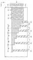
도 1은 본 발명의 일 실시예에 따른 3차원 반도체 기억 소자를 나타내는 단면도.
도 2a는 본 발명의 일 실시예에 따른 3차원 반도체 기억 소자의 일 변형예를 설명하기 위하여 도 1의 A 부분을 확대한 도면.
도 2b는 본 발명의 일 실시예에 따른 3차원 반도체 기억 소자의 다른 변형예를 설명하기 위하여 도 1의 A 부분을 확대한 도면.
도 2c는 본 발명의 일 실시예에 따른 3차원 반도체 기억 소자의 또 다른 변형예를 설명하기 위하여 도 1의 A 부분을 확대한 도면.
도 2d는 본 발명의 일 실시예에 따른 3차원 반도체 기억 소자의 또 다른 변형예를 설명하기 위한 단면도.
도 3a 내지 도 3e는 본 발명의 일 실시예에 따른 3차원 반도체 기억 소자의 제조 방법을 설명하기 위한 단면도들.
도 4a 내지 도 4e는 본 발명의 일 실시예에 따른 3차원 반도체 기억 소자의 제조 방법의 일 변형예를 설명하기 위한 사시도들.
도 5a 내지 도 5c는 본 발명의 일 실시예에 따른 3차원 반도체 기억 소자의 제조 방법의 다른 변형예를 설명하기 위한 단면도들.
도 6은 본 발명의 다른 실시예에 따른 3차원 반도체 기억 소자를 나타내는 단면도.
도 7a는 본 발명의 다른 실시예에 따른 3차원 반도체 기억 소자의 일 변형예를 나타내는 단면도.
도 7b는 본 발명의 다른 실시예에 따른 3차원 반도체 기억 소자의 다른 변형예를 나타내는 단면도.
도 7c는 본 발명의 다른 실시예에 따른 3차원 반도체 기억 소자의 또 다른 변형예를 나타내는 단면도.
도 7d는 본 발명의 다른 실시예에 따른 3차원 반도체 기억 소자의 또 다른 변형예를 나타내는 단면도.
도 7e는 본 발명의 다른 실시예에 따른 3차원 반도체 기억 소자의 또 다른 변형예를 나타내는 단면도.
도 8a 내지 도 8c는 본 발명의 다른 실시예에 따른 3차원 반도체 기억 소자의 제조 방법을 설명하기 위한 단면도들.
도 9a 내지 도 9c는 본 발명의 다른 실시예에 따른 3차원 반도체 기억 소자의 제조 방법의 일 변형예를 설명하기 위한 단면도들.
도 10a 및 도 10b는 본 발명의 다른 실시예에 따른 3차원 반도체 기억 소자의 제조 방법의 다른 변형예를 설명하기 위한 단면도들.
도 11a는 본 발명의 또 다른 실시예에 따른 3차원 반도체 기억 소자를 나타내는 단면도.
도 11b는 본 발명의 또 다른 실시예에 따른 3차원 반도체 기억 소자의 일 변형예를 나타내는 단면도.
도 11c는 본 발명의 또 다른 실시예에 따른 3차원 반도체 기억 소자의 다른 변형예를 나타내는 단면도.
도 12a 및 도 12b는 본 발명의 또 다른 실시예에 따른 3차원 반도체 기억 소자의 제조 방법을 설명하기 위한 단면도들.
도 13a 및 도 13b는 본 발명의 또 다른 실시예에 따른 3차원 반도체 기억 소자의 제조 방법의 변형예를 설명하기 위한 단면도들.
도 14는 본 발명의 기술적 사상에 기초한 3차원 반도체 기억 소자를 포함하는 전자 시스템의 일 예를 간략히 도시한 블록도.
도 15는 본 발명의 기술적 사상에 기초한 3차원 반도체 기억 소자를 포함하는 메모리 카드의 일 예를 간략히 도시한 블록도.1 is a sectional view showing a three-dimensional semiconductor memory device according to an embodiment of the present invention;
FIG. 2A is an enlarged view of a portion A of FIG. 1 for explaining a modified example of a three-dimensional semiconductor memory device according to an embodiment of the present invention; FIG.
FIG. 2B is an enlarged view of a portion A of FIG. 1 to explain another modification of the three-dimensional semiconductor memory device according to the embodiment of the present invention. FIG.
FIG. 2C is an enlarged view of a portion A in FIG. 1 for explaining another modification of the three-dimensional semiconductor memory device according to the embodiment of the present invention; FIG.
FIG. 2D is a sectional view for explaining another modification of the three-dimensional semiconductor memory device according to the embodiment of the present invention; FIG.
FIGS. 3A to 3E are cross-sectional views illustrating a method of manufacturing a three-dimensional semiconductor memory device according to an embodiment of the present invention.
4A to 4E are perspective views for explaining a modified example of a method of manufacturing a three-dimensional semiconductor memory device according to an embodiment of the present invention.
5A to 5C are cross-sectional views for explaining another modification of the method of manufacturing a three-dimensional semiconductor memory device according to an embodiment of the present invention.
6 is a cross-sectional view showing a three-dimensional semiconductor memory device according to another embodiment of the present invention.
7A is a cross-sectional view showing a modification of a three-dimensional semiconductor memory device according to another embodiment of the present invention.
7B is a cross-sectional view showing another modification of the three-dimensional semiconductor memory element according to another embodiment of the present invention;
7C is a sectional view showing still another modification of the three-dimensional semiconductor memory element according to another embodiment of the present invention.
7D is a cross-sectional view showing still another modification of the three-dimensional semiconductor memory element according to another embodiment of the present invention.
7E is a sectional view showing still another modification of the three-dimensional semiconductor memory element according to another embodiment of the present invention.
8A to 8C are cross-sectional views illustrating a method of manufacturing a three-dimensional semiconductor memory device according to another embodiment of the present invention.
9A to 9C are cross-sectional views for explaining a modified example of a method of manufacturing a three-dimensional semiconductor memory device according to another embodiment of the present invention.
10A and 10B are cross-sectional views for explaining another modification of the method for manufacturing a three-dimensional semiconductor memory device according to another embodiment of the present invention.
11A is a cross-sectional view showing a three-dimensional semiconductor memory device according to still another embodiment of the present invention.
11B is a cross-sectional view showing a modification of the three-dimensional semiconductor memory element according to still another embodiment of the present invention.
11C is a cross-sectional view showing another modification of the three-dimensional semiconductor memory element according to still another embodiment of the present invention.
12A and 12B are cross-sectional views illustrating a method for fabricating a three-dimensional semiconductor memory device according to another embodiment of the present invention.
13A and 13B are cross-sectional views for explaining a modification of the method for manufacturing a three-dimensional semiconductor memory device according to another embodiment of the present invention.
14 is a block diagram schematically showing an example of an electronic system including a three-dimensional semiconductor memory element based on the technical idea of the present invention.
15 is a block diagram schematically showing an example of a memory card including a three-dimensional semiconductor memory element based on the technical idea of the present invention.
이상의 본 발명의 목적들, 다른 목적들, 특징들 및 이점들은 첨부된 도면과 관련된 이하의 바람직한 실시예들을 통해서 쉽게 이해될 것이다. 그러나, 본 발명은 여기서 설명되어지는 실시예들에 한정되지 않고 다른 형태로 구체화될 수도 있다. 오히려, 여기서 소개되는 실시예는 개시된 내용이 철저하고 완전해질 수 있도록 그리고 당업자에게 본 발명의 사상이 충분히 전달될 수 있도록 하기 위해 제공되는 것이다.BRIEF DESCRIPTION OF THE DRAWINGS The above and other objects, features, and advantages of the present invention will become more readily apparent from the following description of preferred embodiments with reference to the accompanying drawings. However, the present invention is not limited to the embodiments described herein but may be embodied in other forms. Rather, the embodiments disclosed herein are provided so that the disclosure can be thorough and complete, and will fully convey the scope of the invention to those skilled in the art.
본 명세서에서, 어떤 막(또는 층)이 다른 막(또는 층) 또는 기판 상에 있다고 언급되는 경우에 그것은 다른 막(또는 층) 또는 기판 상에 직접 형성될 수 있거나 또는 그들 사이에 제 3의 막(또는 층)이 개재될 수도 있다 또한, 도면들에 있어서, 구성들의 크기 및 두께 등은 명확성을 위하여 과장된 것이다. 또한, 본 명세서의 다양한 실시예들에서 제1, 제2, 제3 등의 용어가 다양한 영역, 막들(또는 층들) 등을 기술하기 위해서 사용되었지만, 이들 영역, 막들이 이 같은 용어들에 의해서 한정되어서는 안 된다. 이들 용어들은 단지 어느 소정 영역 또는 막(또는 층)을 다른 영역 또는 막(또는 층)과 구별시키기 위해서 사용되었을 뿐이다. 따라서, 어느 한 실시예에의 제1막질로 언급된 막질이 다른 실시예에서는 제2막질로 언급될 수도 있다. 여기에 설명되고 예시되는 각 실시예는 그것의 상보적인 실시예도 포함한다. 본 명세서에서 '및/또는' 이란 표현은 전후에 나열된 구성요소들 중 적어도 하나를 포함하는 의미로 사용된다. 명세서 전체에 걸쳐서 동일한 참조번호로 표시된 부분들은 동일한 구성요소들을 나타낸다.In this specification, when it is mentioned that a film (or layer) is on another film (or layer) or substrate, it may be formed directly on another film (or layer) or substrate, or a third film (Or layer) may be interposed. In the drawings, the sizes and thicknesses of the structures and the like are exaggerated for the sake of clarity. It should also be understood that although the terms first, second, third, etc. have been used in various embodiments herein to describe various regions, films (or layers), etc., It should not be. These terms are merely used to distinguish any given region or film (or layer) from another region or film (or layer). Thus, the membrane referred to as the first membrane in one embodiment may be referred to as the second membrane in another embodiment. Each embodiment described and exemplified herein also includes its complementary embodiment. The expression " and / or " is used herein to mean including at least one of the elements listed before and after. Like numbers refer to like elements throughout the specification.
(제1 실시예)(Embodiment 1)
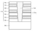
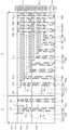
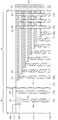
도 1은 본 발명의 일 실시예에 따른 3차원 반도체 기억 소자를 나타내는 단면도이다.1 is a cross-sectional view showing a three-dimensional semiconductor memory device according to an embodiment of the present invention.
도 1을 참조하면, 반도체 기판(100, 이하 기판이라 함) 상에 복수의 적층 구조체들(115, 215, 315, 415)이 차례로 적층될 수 있다. 구체적으로, 제1 적층 구조체(115)가 배치될 수 있다. 예컨대, 상기 기판(100)은 실리콘 기판, 게르마늄 기판, 또는 실리콘-게르마늄 기판 등일 수 있다. 상기 제1 적층 구조체(115, stacked structure)는 교대로 그리고 반복적으로 적층된 제1 절연 패턴들(105) 및 제1 게이트 패턴들(110)을 포함할 수 있다. 복수의 제1 수직형 활성 패턴들(130)이 상기 기판(100)의 상부면에 실질적으로 수직한 방향으로 연장되어, 상기 제1 적층 구조체(115)를 관통할 수 있다. 상기 제1 수직형 활성 패턴들(130)은 서로 옆으로 이격될 수 있다. 상기 제1 수직형 활성 패턴들(130)은 상기 기판(100)과 접속될 수 있다. 상기 제1 수직형 활성 패턴들(130)은 일 방향으로 배열될 수 있다. 제1 데이터 저장막(125)이 상기 제1 수직형 활성 패턴(130)의 측벽과 상기 각 제1 게이트 패턴(110) 사이에 개재될 수 있다. 일 실시예에 따르면, 상기 제1 데이터 저장막(125)은 실질적으로 수직으로 연장되어 상기 제1 수직형 활성 패턴(130)의 측벽과 상기 제1 절연 패턴(105) 사이에 개재될 수 있다. 상기 제1 게이트 패턴들(110)은 수직형 트랜지스터들의 게이트들에 해당할 수 있다. 상기 수직형 트랜지스터는 상기 각 제1 게이트 패턴(110)에 인접한 상기 제1 수직형 활성 패턴(130)의 측벽에 정의되는 수직형 채널 영역을 포함할 수 있다.Referring to FIG. 1, a plurality of
상기 제1 게이트 패턴들(110)은 도전 물질을 포함할 수 있다. 예컨대, 상기 제1 게이트 패턴들(110)은 도핑된 반도체(ex, 도핑된 실리콘 등), 도전성 금속질화물(ex, 질화티타늄, 질화탄탈늄 등), 금속(ex, 텅스텐, 알루미늄 등), 전이금속(ex, 티타늄, 탄탈늄등), 또는 금속-반도체 화합물(ex, 금속 실리사이드 등) 등에서 적어도 하나를 포함할 수 있다. 상기 제1 절연 패턴들(105)은 산화물, 질화물 및/또는 산화질화물 등을 포함할 수 있다. 상기 제1 수직형 활성 패턴(130)은 상기 기판(100)과 동일한 반도체 물질을 포함할 수 있다. 예컨대, 상기 기판(100)이 실리콘 기판인 경우에, 상기 제1 수직형 활성 패턴(130)은 실리콘으로 형성될 수 있다. 상기 제1 수직형 활성 패턴(130)은 다결정 상태 또는 단결정 상태일 수 있다. 일 실시예에 따르면, 상기 제1 수직형 활성 패턴들(130)은 도 1에 개시된 바와 같이 필라 형태(pillar-shaped)일 수 있다. 하지만, 본 발명은 여기에 한정되지 않는다.The
상기 제1 데이터 저장막(125)은 터널 절연막, 전하저장층 및 블로킹 절연막을 포함할 수 있다. 상기 터널 절연막은 산화물을 포함할 수 있다. 상기 전하저장층은, 전하를 저장하는 트랩들을 갖는 유전 물질을 포함할 수 있다. 예컨대, 상기 전하저장층은 질화물을 포함할 수 있다. 상기 블로킹 절연막은 상기 터널 절연막에 비하여 높은 유전상수를 갖는 고유전막을 포함할 수 있다. 예컨대, 상기 블로킹 절연막은 알루미늄 산화막 및/또는 하프늄 산화막 등과 같은 금속 산화막을 포함할 수 있다. 이에 더하여, 상기 블로킹 절연막은 상기 고유전막에 비하여 에너지 밴드갭이 더 큰 장벽 절연막(ex, 산화막)을 더 포함할 수 있다. 상기 전하저장층은 상기 터널 절연막 및 블로킹 절연막 사이에 배치될 수 있다. 상기 터널 절연막은 상기 제1 수직형 활성 패턴(130)의 측벽 및 상기 전하저장층 사이에 배치될 수 있으며, 상기 블로킹 절연막은 상기 전하저장층, 및 상기 제1 수직형 활성 패턴(130)의 측벽에 인접한 상기 제1 게이트 패턴(110)의 일 측벽 사이에 개재될 수 있다. 상기 블로킹 절연막이 상기 장벽 절연막 및 상기 고유전막을 포함하는 경우에, 상기 장벽 절연막은 상기 전하저장층 및 상기 고유전막 사이에 개재될 수 있다.The first
상기 제1 게이트 패턴들(110)의 각각은 상기 일 방향으로 연장된 패드부(112)를 포함할 수 있다. 상기 제1 게이트 패턴들(110)의 패드부들(112)은 계단식 구조로 형성될 수 있다. 제1 평탄화된 유전막(135)이 상기 제1 게이트 패턴들(110)의 패드부들(112) 상에 배치될 수 있다. 즉, 상기 제1 평탄화된 유전막(135)이 상기 제1 게이트 패턴들(110)의 패드부들(112)을 덮을 수 있다. 상기 제1 평탄화된 유전막(135)은 상기 제1 수직형 활성 패턴(130)의 상부면들, 및 제1 적층 구조체(115)내 최상위의 제1 절연 패턴의 상부면과 실질적으로 공면(coplanar)을 이룰 수 있다.Each of the
상기 제1 적층 구조체(115) 상에 제2 적층 구조체(215)가 배치될 수 있다. 상기 제2 적층 구조체(215)는 교대로 그리고 반복적으로 적층된 제2 절연 패턴들(205) 및 제2 게이트 패턴들(210)을 포함할 수 있다. 복수의 제2 수직형 활성 패턴들(230)이 상기 제2 적층 구조체(215)를 관통할 수 있다. 제2 데이터 저장막(225)이 상기 각 제2 수직형 활성 패턴(230)의 측벽 및 상기 각 제2 게이트 패턴(210) 사이에 개재될 수 있다. 상기 제2 게이트 패턴들(210)의 각각은 상기 일 방향으로 연장된 패드부(212)를 포함할 수 있다. 상기 제2 게이트 패턴들(210)의 패드부들(212)은 상기 제1 게이트 패턴들(110)의 패드부들(112)과 함께 계단식 구조를 형성될 수 있다.A
상기 제2 수직형 활성 패턴들(230)은 상기 제1 수직형 활성 패턴들(130)의 상부면들 상에 접속될 수 있다. 이때, 상기 제1 수직형 활성 패턴들(130)의 개수는 상기 제2 수직형 활성 패턴들(230)의 개수 보다 많을 수 있다. 이에 따라, 상기 복수의 제1 수직형 활성 패턴들(130)은 상기 제2 수직형 활성 패턴들(230)과 접속된(connected) 제1 수직형 활성 패턴들(130), 및 상기 제2 수직형 활성 패턴들(230)과 비-접속된(non-connected) 제1 수직형 활성 패턴(130)을 포함할 수 있다. 상기 비-접속된 제1 수직형 활성 패턴(130)은 하나 이상일 수 있다. 상기 접속된 수직형 활성 패턴(130)과 상기 제1 게이트 패턴들(110)의 패드부들(112) 사이에 배치될 수 있다. 일 실시예에 따르면, 상기 비-접속된 제1 수직형 활성 패턴(130)의 상부면은 최하위에 배치된 제2 게이트 패턴(210)에 의하여 덮혀질 수 있다.The second vertical
제2 평탄화된 유전막(235)이 상기 제2 게이트 패턴들(210)의 패드부들(212) 상 및 상기 제1 평탄화된 유전막(135) 상에 배치될 수 있다. 상기 제2 평탄화된 유전막(235)은 상기 제2 수직형 활성 패턴들(230)의 상부면들과 실질적으로 공면을 이룰 수 있다. 또한, 상기 제2 평탄화된 유전막(235)은 상기 제2 적층 구조체(215) 내에서 최상위층에 위치한 제2 절연 패턴의 상부면과 공면을 이룰 수 있다.A second
상기 제2 게이트 패턴(210), 제2 수직형 활성 패턴(230) 및 제2 데이터 저장막(225)은 각각 상기 제1 게이트 패턴(110), 제1 수직형 활성 패턴(130) 및 제1 데이터 저장막(125)과 동일한 물질로 형성될 수 있다. 이와 마찬가지로, 상기 제2 절연 패턴(205)도 상기 제1 절연 패턴(105)과 동일한 물질로 형성될 수 있다. 상기 제2 평탄화된 유전막(235)은 산화물, 질화물 및/또는 산화질화물 등을 포함할 수 있다. 상기 제2 평탄화된 유전막(235)은 상기 제1 평탄화된 유전막(135)과 동일한 물질로 형성될 수 있다.The
제3 적층 구조체(315)가 상기 제2 적층 구조체(215) 상에 배치될 수 있다. 상기 제3 적층 구조체(315)는 교대로 그리고 반복적으로 적층된 제3 절연 패턴들(305) 및 제3 게이트 패턴들(310)을 포함할 수 있다. 복수의 제3 수직형 활성 패턴들(330)이 상기 제3 적층 구조체(315)를 관통할 수 있다. 제3 데이터 저장막(325)이 상기 각 제3 수직형 활성 패턴(330)의 측벽 및 상기 각 제3 게이트 패턴(310) 사이에 개재될 수 있다. 상기 제3 게이트 패턴들(310)의 각각은 상기 일 방향으로 연장된 패드부(312)를 포함할 수 있다. 상기 제3 게이트 패턴들(310)의 패드부들(312)은 상기 제1 및 제2 게이트 패턴들(110, 210)의 패드부들(112, 212)과 함께 계단식 구조를 이룰 수 있다.A
일 실시예에 따르면, 상기 제3 수직형 활성 패턴들(330)의 개수는 상기 제2 수직형 활성 패턴들(230)의 개수 보다 많을 수 있다. 상기 복수의 제2 수직형 활성 패턴들(230)은 상기 제3 수직형 활성 패턴들(330)과 접속된 제2 수직형 활성 패턴들(230), 및 상기 제3 수직형 활성 패턴들(330)과 비-접속된 적어도 하나의 제2 수직형 활성 패턴(230)을 포함할 수 있다. 상기 비-접속된 제2 수직형 활성 패턴(230)은 상기 접속된 제2 수직형 활성 패턴(230)과 상기 제2 게이트 패턴들(210)의 패드부들(212) 사이에 배치될 수 있다. 일 실시예에 따르면, 상기 비-접속된 제2 수직형 활성 패턴(230)의 상부면은 최하위에 배치된 제3 게이트 패턴(310)에 의하여 덮혀질 수 있다.According to one embodiment, the number of the third
제3 평탄화된 유전막(335)이 상기 제3 게이트 패턴들(310)의 패드부들(312) 및 제2 평탄화된 유전막(235)을 덮을 수 있다. 상기 제3 평탄화된 유전막(335)의 상부면은 상기 제3 수직형 활성 패턴들(330)의 상부면들과 실질적으로 공면을 이룰 수 있다. 상기 제3 게이트 패턴(310), 제3 절연 패턴(305), 제3 수직형 활성 패턴(330), 제3 데이터 저장막(325) 및 제3 평탄화된 유전막(335)은 각각 제1 게이트 패턴(110), 제1 절연 패턴(105), 제1 수직형 활성 패턴(130), 제1 데이터 저장막(325) 및 제1 평탄화된 유전막(135)과 동일한 물질로 형성될 수 있다.A third planarized
제4 적층 구조체(415)가 상기 제3 적층 구조체(315) 상에 배치될 수 있다. 상기 제4 적층 구조체(415)는 교대로 그리고 반복적으로 적층된 제4 절연 패턴들(405) 및 제4 게이트 패턴들(410)을 포함할 수 있다. 복수의 제4 수직형 활성 패턴들(430)이 상기 제4 적층 구조체(415)를 관통할 수 있다. 제4 데이터 저장막(425)이 상기 각 제3 수직형 활성 패턴(430)의 측벽 및 상기 각 제4 게이트 패턴(410) 사이에 개재될 수 있다. 상기 제4 게이트 패턴들(410)의 각각은 상기 일 방향으로 연장된 패드부(412)를 포함할 수 있다. 상기 제4 게이트 패턴들(410)의 패드부들(412)은 상기 제1, 제2 및 제3 게이트 패턴들(110, 210, 310)의 패드부들(112, 212, 312)과 함께 계단식 구조를 이룰 수 있다.A
일 실시예에 따르면, 상기 제4 수직형 활성 패턴들(430)의 개수는 상기 제3 수직형 활성 패턴들(330)의 개수 보다 많을 수 있다. 상기 복수의 제3 수직형 활성 패턴들(330)은 상기 제4 수직형 활성 패턴들(430)과 접속된 제3 수직형 활성 패턴들(330), 및 상기 제4 수직형 활성 패턴들(430)과 비-접속된 적어도 하나의 제3 수직형 활성 패턴(330)을 포함할 수 있다. 상기 비-접속된 제3 수직형 활성 패턴(330)은 상기 접속된 제3 수직형 활성 패턴(330)과 상기 제3 게이트 패턴들(310)의 패드부들(312) 사이에 배치될 수 있다. 일 실시예에 따르면, 상기 비-접속된 제3 수직형 활성 패턴(330)의 상부면은 최하위에 배치된 제4 게이트 패턴(410)에 의하여 덮혀질 수 있다.According to one embodiment, the number of the fourth
제4 평탄화된 유전막(435)이 상기 제4 게이트 패턴들(410)의 패드부들(412) 및 제3 평탄화된 유전막(335) 상에 배치될 수 있다. 상기 제4 평탄화된 유전막(435)의 상부면은 상기 제4 수직형 활성 패턴들(430)의 상부면들과 실질적으로 공면을 이룰 수 있다. 상기 제4 게이트 패턴(410), 제4 절연 패턴(405), 제4 수직형 활성 패턴(430), 제4 데이터 저장막(425) 및 제4 평탄화된 유전막(435)은 각각 제1 게이트 패턴(110), 제1 절연 패턴(105), 제1 수직형 활성 패턴(130), 제1 데이터 저장막(325) 및 제1 평탄화된 유전막(135)과 동일한 물질로 형성될 수 있다.A fourth planarized
상기 제2, 제3 및 제4 수직형 활성 패턴들(230, 330, 430)은 상기 제1 수직형 활성 패턴(130)과 동일한 형태일 수 있으며, 상기 제2, 제3 및 제4 데이터 저장막들(225, 325, 425)은 상기 제1 데이터 저장막(125)과 동일한 형태일 수 있다.The second, third, and fourth vertical
상기 제1 게이트 패턴들(110) 중에서 최하위에 위치한 제1 게이트 패턴은 접지 선택 트랜지스터의 게이트에 해당할 수 있으며, 상기 제4 게이트 패턴들(410) 중에서 최상위에 위치한 제4 게이트 패턴은 스트링 선택 트랜지스터의 게이트에 해당할 수 있다. 상기 최하위의 제1 게이트 패턴 및 상기 최상위의 제4 게이트 패턴 사이에 개재된 제1, 제2, 제3 및 제4 게이트 패턴들(110, 210, 310, 410)은 셀 트랜지스터들의 게이트들에 해당할 수 있다. 상기 각 셀 트랜지스터는 데이터 저장막(125, 225, 325 또는 425)의 전하저장층을 정보 저장 요소로 사용할 수 있다. 이에 따라, 상기 각 셀 트랜지스터는 비휘발성 기억 셀로 구현될 수 있다. 서로 접속되고 적층된 제1, 제2, 제3 및 제4 수직형 활성 패턴들(130, 230, 330, 430)은 하나의 수직형 셀 스트링으로 구현될 수 있다. 상기 제4 수직형 활성 패턴(430)과 비-접속된 제1, 제2 및 제3 수직형 활성 패턴들(130, 230, 330)은 셀 스트링 이외의 다른 트랜지스터들로 구현될 수 있다. 이와는 달리, 상기 제4 수직형 활성 패턴(430)과 비-접속된 제1, 제2 및 제3 수직형 활성 패턴들(130, 230, 330)은 더미 패턴들일 수도 있다.The first gate pattern positioned at the lowermost one of the
상술한 3차원 반도체 기억 소자에 따르면, 복수의 적층 구조체들(115, 215, 315, 415) 중에서 상대적으로 낮은 레벨에 위치한 적층 구조체를 관통하는 수직형 활성 패턴들의 개수가 상대적으로 높은 레벨에 위치한 적층 구조체를 관통하는 수직형 활성 패턴들의 개수 보다 많을 수 있다. 이에 따라, 3차원 반도체 기억 소자의 평탄화 공정을 보다 용이하게 수행할 수 있다.According to the above-described three-dimensional semiconductor memory device, the number of vertical active patterns passing through the stacked structure located at a relatively low level among the plurality of
예컨대, 상기 제1, 제2, 제3 및 제4 게이트 패턴들(110, 210, 310, 410)의 패드부들(112, 212, 312, 412)은 계단식 구조를 갖는다. 이로 인하여, 만약, 상기 비-접속된 활성 패턴들이 생략되는 경우에, 상기 접속된 제1 수직형 활성 패턴과 제1 게이트 패턴들(110)의 패드부들(112)간의 거리는 상기 제4 수직형 활성 패턴(430)과 상기 제4 게이트 패턴들(410)의 패드부들(412)간의 거리에 비하여 월등히 클 수 있다. 이에 따라, 제1 평탄화된 유전막(135)을 평탄화하는 과정에서 디슁(dishing) 현상 등이 발생되어, 3차원 반도체 기억 소자의 신뢰성이 저하될 수 있다. 하지만, 본 발명의 실시예에 따르면, 낮은 레벨의 적층 구조체를 관통하는 수직형 활성 패턴의 개수가 높은 레벨의 적층 구조체를 관통하는 수직형 활성 패턴의 개수 보다 많음으로써, 상술된 평탄화 공정에 의한 신뢰성을 저하를 최소화할 수 있다. 결과적으로, 우수한 신뢰성을 갖고 고집적화에 최적화된 반도체 기억 소자를 구현할 수 있다.For example, the
상술된 바와 같이, 본 실시예에서는, 4개의 적층 구조체들(115, 215, 315, 415)이 차례로 적층될 수 있다. 하지만, 본 발명은 여기에 한정되지 않는다. 상기 기판(100) 상에는 2개 이상의 적층 구조체들이 적층될 수 있다.As described above, in this embodiment, four stacking
상술된 3차원 반도체 기억 소자에서, 수직형 활성 패턴은 필라 형태일 수 있으며, 데이터 유전막은 연장되어 수직형 활성 패턴과 절연 패턴 사이에 개재될 수 있다. 이와는 다르게, 상기 수직형 활성 패턴은 다른 형태를 가질 수 있으며, 상기 데이터 유전막도 다른 형태를 가질 수 있다. 이러한 변형예들을 도면들을 참조하여 설명한다.In the three-dimensional semiconductor memory element described above, the vertical active pattern may be in the form of a pillar, and the data dielectric layer may extend between the vertical active pattern and the insulating pattern. Alternatively, the vertical active pattern may have a different shape, and the data dielectric layer may have another shape. These modifications will be described with reference to the drawings.
도 2a는 본 발명의 일 실시예에 따른 3차원 반도체 기억 소자의 일 변형예를 설명하기 위하여 도 1의 A 부분을 확대한 도면이다.2A is an enlarged view of a portion A of FIG. 1 for explaining a modified example of a three-dimensional semiconductor memory device according to an embodiment of the present invention.
도 2a를 참조하면, 본 변형예에 따른 제1 수직형 활성 패턴(130a)은 내부가 비어 있는 마카로니 형태(macaroni-shaped)일 수 있다. 이 경우에, 상기 제1 수직형 활성 패턴(130a)의 내부는 충전 유전 패턴(131)으로 채워질 수 있다. 상기 충전 유전 패턴(131)은 산화물, 질화물 및/또는 산화질화물 등을 포함할 수 있다. 캐핑 반도체 패턴(132)이 상기 충전 유전 패턴(131) 상에 배치될 수 있다. 상기 캐핑 반도체 패턴(132)은 상기 제1 수직형 활성 패턴(130a)과 접촉될 수 있다. 상기 제1 수직형 활성 패턴(130a)은 도 1의 제1 수직형 활성 패턴(130)과 동일한 반도체 물질로 형성될 수 있으며, 상기 캐핑 반도체 패턴(132)은 상기 제1 수직형 활성 패턴(130a)과 동일한 물질로 형성될 수 있다. 도 1의 제2, 제3 및 제4 수직형 활성 패턴들(230, 330, 430)은 본 변형예에서 설명한 상기 제1 수직형 활성 패턴(130a)과 동일한 형태를 가질 수 있다.Referring to FIG. 2A, the first vertical
도 2b는 본 발명의 일 실시예에 따른 3차원 반도체 기억 소자의 다른 변형예를 설명하기 위하여 도 1의 A 부분을 확대한 도면이다.FIG. 2B is an enlarged view of a portion A of FIG. 1 to explain another modification of the three-dimensional semiconductor memory device according to an embodiment of the present invention.
도 2b를 참조하면, 본 변형예에 따르면, 제1 데이터 유전막(125a)은 제1 수직형 활성 패턴(130)의 측벽과 제1 게이트 패턴(110) 사이에 개재될 수 있다. 상기 제1 데이터 유전막(125a)은 연장되어 상기 제1 게이트 패턴(110)과, 상기 제1 게이트 패턴(110)에 인접한 제1 절연 패턴(105) 사이에 개재될 수 있다. 상기 제1 데이터 유전막(125a)의 연장된 부분들은 상기 제1 게이트 패턴(110)의 하부면 및 상부면과 접촉될 수 있다. 상기 제1 데이터 유전막(125a)은 도 1을 참조하여 설명한 제1 데이터 유전막(125)과 동일한 물질로 형성될 수 있다. 본 변형예에서, 상기 제1 수직형 활성 패턴(130)은 도 2a에 개시된 제1 수직형 활성 패턴(130a)과 대체될 수 있다. 도 1에 개시된 제2, 제3 및 제4 데이터 유전막들(225, 325, 425)도 도 2b에 개시된 제1 데이터 유전막(125a)과 동일한 형태를 가질 수 있다.Referring to FIG. 2B, according to this modification, the first
도 2c는 본 발명의 일 실시예에 따른 3차원 반도체 기억 소자의 또 다른 변형예를 설명하기 위하여 도 1의 A 부분을 확대한 도면이다.FIG. 2C is an enlarged view of a portion A of FIG. 1 to explain another modification of the three-dimensional semiconductor memory device according to an embodiment of the present invention.
도 2c를 참조하면, 본 변형예에 따른 제1 데이터 유전막(125b)은 제1 서브막(127, first sub layer) 및 제2 서브막(128, second sub layer)을 포함할 수 있다. 상기 제1 데이터 유전막(125b)은 제1 수직형 활성 패턴(130)의 측벽 및 제1 게이트 패턴(110) 사이에 개재될 수 있다. 이때, 상기 제1 서브막(127)은 연장되어 상기 제1 수직형 활성 패턴(130)의 측벽과 제1 절연 패턴(105) 사이에 개재될 수 있다. 상기 제2 서브막(128)은 연장되어 상기 제1 게이트 패턴(105)과, 상기 제1 게이트 패턴(105)에 인접한 제1 절연 패턴(105) 사이에 개재될 수 있다. 상기 제2 서브막(128)의 연장된 부분들은 상기 제1 게이트 패턴(105)의 상부면 및 하부면에 접촉될 수 있다.Referring to FIG. 2C, the first
상기 제1 데이터 저장막(125b)은 도 1의 제1 데이터 저장막(125)과 같이 터널 절연막, 전하 저장층 및 블로킹 절연막을 포함할 수 있다. 이때, 상기 제1 서브막(127)은 상기 터널 절연막, 전하 저장층 및 블로킹 절연막 중에서 일부분을 포함할 수 있으며, 상기 제2 서브막(128)은 다른 부분을 포함할 수 있다. 상기 제1 서브막(127)은 적어도 상기 터널 절연막을 포함할 수 있으며, 상기 제2 서브막(128)은 적어도 상기 블로킹 절연막의 일부분을 포함할 수 있다. 예를 들면, 상기 제1 서브막(127)은 상기 터널 절연막, 전하 저장층, 및 상기 블로킹 유전막의 장벽 절연막을 포함할 수 있으며, 상기 제2 서브막(128)은 상기 블로킹 유전막의 고유전막을 포함할 수 있다. 하지만, 본 발명은 여기에 한정되지 않는다. 상기 제1 서브막(127) 및 제2 서브막(128)은 다른 형태로 구현될 수도 있다.The first
본 변형예에서, 상기 제1 수직형 활성 패턴(130)은 도 2a의 수직형 활성 패턴(130a)으로 대체될 수 있다. 도 1의 제2, 제3 및 제4 데이터 저장막들(225, 325, 425)은 상기 제1 데이터 저장막(125b)과 동일한 형태로 구현될 수 있다.In this modification, the first
한편, 상술된 도 1의 3차원 반도체 기억 소자에 따르면, 상기 적층 구조체들이 높아질수록, 수직형 활성 패턴들의 개수가 점진적으로 감소될 수 있다. 이와는 다르게, 수직형 활성 패턴들의 개수는 다른 방식으로 구현될 수도 있다. 이를 도 2d를 참조하여 설명한다.On the other hand, according to the three-dimensional semiconductor memory element of Fig. 1 described above, the higher the number of the stacked structures, the more gradually the number of vertical active patterns can be reduced. Alternatively, the number of vertical active patterns may be implemented in other ways. This will be described with reference to FIG. 2D.
도 2d는 본 발명의 일 실시예에 따른 3차원 반도체 기억 소자의 또 다른 변형예를 설명하기 위한 단면도이다.2D is a cross-sectional view for explaining another modification of the three-dimensional semiconductor memory device according to the embodiment of the present invention.
도 2d를 참조하면, 제1 적층 구조체(115)가 기판(100) 상에 배치될 수 있다. 하부 적층 구조체(115L)가 상기 제1 적층 구조체(115) 및 기판(100) 사이에 개재될 수 있다. 상기 하부 적층 구조체(115L)는 교대로 그리고 반복적으로 적층된 하부 절연 패턴들(105L) 및 하부 게이트 패턴들(110L)을 포함할 수 있다. 상기 하부 게이트 패턴들(110L)의 각각은 패드부(112L)을 포함할 수 있다. 복수의 하부 수직형 활성 패턴들(130L)이 상기 하부 적층 구조체(115L)를 관통할 수 있다. 하부 데이터 유전막(125L)이 상기 하부 수직형 활성 패턴(130L)의 측벽 및 상기 각 하부 게이트 패턴(110L) 사이에 개재될 수 있다. 상기 복수의 하부 수직형 활성 패턴들(130L)의 개수는 상기 제1 수직형 활성 패턴들(130)의 개수와 동일할 수 있다. 상기 제1 수직형 활성 패턴들(130)은 상기 하부 수직형 활성 패턴들(130L) 상에 각각 접속될 수 있다.Referring to FIG. 2D, a
상기 제1 게이트 패턴들(110)의 패드부들(112) 및 하부 게이트 패턴들(110L)의 패드부들(112L)은 계단식 구조를 이룬다. 제1 평탄화된 유전막(150)이 상기 제1 게이트 패턴들(110)의 패드부들(112) 및 하부 게이트 패턴들(110L)의 패드부들(112L)을 덮는다. 상기 제1 평탄화된 유전막(150)의 상부면은 상기 제1 수직형 활성 패턴들(130)의 상부면들과 실질적으로 공면을 이룰 수 있다. 상기 하부 게이트 패턴(110L), 하부 절연 패턴(105L), 하부 수직형 활성 패턴(130L) 및 하부 데이터 유전막(125L)은 각각 제1 게이트 패턴(110), 제1 절연 패턴(105), 제1 수직형 활성 패턴(130) 및 제1 데이터 유전막(125)과 동일한 물질로 형성될 수 있다. 상기 제1 평탄화된 유전막(150)은 산화물, 질화물 및/또는 산화질화물 등을 포함할 수 있다.The
제2 적층 구조체(215)가 상기 제1 적층 구조체(115) 상에 배치될 수 있다. 상기 제1 수직형 활성 패턴들(130)의 개수는 상기 제2 적층 구조체(215)를 관통하는 복수의 제2 수직형 활성 패턴들(230)의 개수 보다 많을 수 있다.And a
상부 적층 구조체(215U)가 상기 제2 적층 구조체(215) 상에 배치될 수 있다. 상기 상부 적층 구조체(215U)은 교대로 그리고 반복적으로 적층된 상부 절연 패턴들(205U) 및 상부 게이트 패턴들(210U)을 포함할 수 있다. 상기 각 게이트 패턴(210U)은 일 방향으로 연장된 패드부(212U)를 포함할 수 있다. 복수의 상부 수직형 활성 패턴(230U)이 상기 상부 적층 구조체(215U)를 관통할 수 있다. 상부 데이터 유전막(225U)이 상기 상부 수직형 활성 패턴(230U)의 측벽 및 상기 각 상부 게이트 패턴(210U) 사이에 개재될 수 있다. 상기 상부 수직형 활성 패턴들(230U)의 개수는 상기 제2 수직형 활성 패턴들(230)의 개수와 동일할 수 있다. 따라서, 상기 상부 수직형 활성 패턴들(230U)은 상기 제2 수직형 활성 패턴들(230) 상에 각각 접속될 수 있다.The upper
상기 상부 게이트 패턴들(210U)의 패드부들(212U), 제2 게이트 패턴들(210)의 패드부들(212), 제1 게이트 패턴들(110)의 패드부들(112) 및 하부 게이트 패턴들(110L)의 패드부들(112L)은 계단식 구조를 이룰 수 있다. 제2 평탄화된 유전막(250)이 상기 상부 게이트 패턴들(210U)의 패드부들(212U) 및 제2 게이트 패턴들(210)의 패드부들(212) 및 제1 평탄화된 유전막(150) 상에 배치될 수 있다. 상기 제2 평탄화된 유전막(250)의 상부면은 상기 상부 수직형 활성 패턴들(230U)의 상부면들과 실질적으로 공면을 이룰 수 있다. 상기 상부 게이트 패턴(210U), 상부 절연 패턴(205U), 상부 수직형 활성 패턴(230U) 및 상부 데이터 유전막(225U)은 각각 제2 게이트 패턴(210), 제2 절연 패턴(205), 제2 수직형 활성 패턴(230) 및 제2 데이터 유전막(225)과 동일한 물질로 형성될 수 있다. 상기 제2 평탄화된 유전막(250)은 산화물, 질화물 및/또는 산화질화물 등을 포함할 수 있다.The
도 3a 내지 도 3e는 본 발명의 일 실시예에 따른 3차원 반도체 기억 소자의 제조 방법을 설명하기 위한 단면도들이다.3A to 3E are cross-sectional views illustrating a method of manufacturing a three-dimensional semiconductor memory device according to an embodiment of the present invention.
도 3a를 참조하면, 상에 제1 절연막들(105) 및 제1 게이트막들(110)을 교대로 그리고 반복적으로 형성할 수 있다.Referring to FIG. 3A, the first insulating
도 3b를 참조하면, 상기 적층된 제1 절연막들(105) 및 제1 게이트막들(110)을 관통하는 제1 채널 홀들을 형성하고, 상기 제1 채널 홀들의 측벽 상에 제1 데이터 저장막(125)을 형성할 수 있다. 이어서, 상기 각 제1 채널 홀 내에 제1 수직형 활성 패턴(130)을 형성할 수 있다. 도시된 바와 같이, 상기 제1 수직형 활성 패턴(130)은 상기 제1 채널 홀을 채우는 필라 형태로 형성될 수 있다.Referring to FIG. 3B, first channel holes passing through the first insulating
이와는 다르게, 상기 제1 데이터 저장막(125)을 갖는 기판(100) 상에 제1 반도체막을 콘포말하게 형성하고, 상기 제1 반도체막 상에 상기 제1 채널 홀들을 채우는 충전 유전막을 형성할 수 있다. 이어서, 상기 충전 유전막 및 제1 반도체막을 평탄화시키어, 도 2a에 개시된 바와 같이, 마카로니 형태의 제1 수직형 활성 패턴(130a) 및 충전 유전 패턴(131)을 형성할 수 있다. 이어서, 상기 제1 수직형 활성 패턴(130a) 및 충전 유전 패턴(131)의 상단을 상기 제1 채널 홀의 상단 보다 낮게 리세스시킬 수 있다. 이어서, 상기 기판(100) 상에 제2 반도체막을 형성하고, 상기 제2 반도체막을 평탄화시키어, 도 2a의 캐핑 반도체 패턴(132)을 형성할 수 있다.Alternatively, a first semiconductor film may be conformally formed on a
도 3c를 참조하면, 상기 제1 절연막들(105) 및 제1 게이트막들을 패터닝하여 계단식 구조의 패드들(112)을 갖는 제1 게이트 패턴들(110)을 형성할 수 있다. 이로써, 교대로 그리고 반복적으로 적층된 제1 절연 패턴들(105) 및 제1 게이트 패턴들(110)을 갖는 제1 적층 구조체(115)를 형성할 수 있다. 상기 계단식 구조의 패드들(112)은 마스크 패턴을 소모적 식각 마스크로 사용하는 제1 패터닝 공정에 의하여 형성될 수 있다. 이와는 다르게, 상기 계단식 구조의 패드들(112)은 기준 마스크 패턴에 마스크 스페이서들을 단계적으로 추가하는 마스킹 기법(masking method)을 사용하는 제2 패터닝 공정에 의하여 형성될 수 있다. 상기 제1 및 제2 패터닝 공정들의 구체적인 방법은 도 12 및 도 13을 참조하여 후술한다.Referring to FIG. 3C, the first insulating
계속해서, 도 3c를 참조하면, 이어서, 제1 유전막을 기판(100) 전면 상에 형성하고, 상기 제1 유전막을 상기 제1 수직형 활성 패턴들(130)이 노출될 때까지 평탄화시킨다. 이에 따라, 제1 평탄화된 유전막(135)이 형성될 수 있다. 상기 제1 평탄화된 유전막(135)은 상기 제1 게이트 패턴들(110)의 패드부들(112)을 덮는다. 상기 제1 유전막의 평탄화 공정 시에, 상기 제1 수직형 활성 패턴들(130)의 상부면을 식각 정지층으로 사용함으로써, 상기 제1 평탄화된 유전막(135)은 상기 제1 수직형 활성 패턴들(130)의 상부면들과 실질적으로 공면을 이룰 수 있다.Next, referring to FIG. 3C, a first dielectric layer is formed on the entire surface of the
도 3d를 참조하면, 상기 제1 평탄된 유전막(135)을 갖는 기판(100) 상에 교대로 그리고 반복적으로 적층된 제2 절연막들(205) 및 제2 게이트막들(210)을 형성할 수 있다. 상기 제2 절연막들(205) 및 제2 게이트막들(210)을 관통하는 제2 채널 홀들을 형성할 수 있다. 상기 제2 채널 홀은 상기 제1 수직형 활성 패턴(130)을 노출시킬 수 있다. 상기 제2 채널 홀의 측벽 상에 제2 데이터 저장막(225)을 형성할 수 있으며, 이어서, 상기 제2 채널 홀 내에 제2 수직형 활성 패턴(230)을 형성할 수 있다. 상기 제2 수직형 활성 패턴(230)은 상기 제1 수직형 활성 패턴(130) 상에 접속될 수 있다. 이때, 상기 제2 채널 홀들의 개수는 상기 제1 채널 홀들의 개수보다 작을 수 있다. 이에 따라, 상기 제1 수직형 활성 패턴들(130)은 상기 제2 수직형 활성 패턴들(230)과 접속된 제1 수직형 활성 패턴들, 및 상기 제2 수직형 활성 패턴(230)과 비-접속된 적어도 하나의 제1 수직형 활성 패턴을 포함할 수 있다. 상기 비-접속된 제1 수직형 활성 패턴은 상기 제2 수직형 활성 패턴(230)과 접속된 제1 수직형 활성 패턴, 및 제1 게이트 패턴들(110)의 패드부들(112) 사이에 개재될 수 있다. 상기 제2 수직형 활성 패턴들(230)은 상기 제1 수직형 활성 패턴들(130)과 동일한 형태로 형성될 수 있다.Referring to FIG. 3D, the second insulating
이어서, 상기 제2 절연막들(205) 및 제2 게이트막들(210)을 패터닝하여, 계단식 구조의 패드부들(212)을 갖는 제2 게이트 패턴들(210)을 형성할 수 있다. 이로써, 교대로 그리고 반복적으로 적층된 제2 절연 패턴들(205) 및 제2 게이트 패턴들(210)을 갖는 제2 적층 구조체(215)를 형성할 수 있다. 상기 제2 게이트 패턴들(210)의 패드부들(212)은 상기 제1 게이트 패턴들(110)의 패드부들(112)과 함께 계단식 구조를 이룰 수 있다. 다시 말해서, 상기 최상위의 제2 게이트 패턴(210)의 패드부(212)로부터 최하위의 제1 게이트 패턴(110)의 패드부(212)를 향하여 내리막 계단식 구조로 형성될 수 있다. 상기 제2 수직형 활성 패턴(230)과 비-접속된 제1 수직형 활성 패턴은 상기 제2 게이트 패턴들(210)의 패드부들(212) 아래에 위치할 수 있다.The second insulating
이어서, 제2 유전막을 기판(100) 상에 형성하고, 상기 제2 유전막을 상기 제2 수직형 활성 패턴들(230)이 노출될 때까지 평탄화시키어, 제2 평탄화된 유전막(235)을 형성할 수 있다.A second dielectric layer is then formed on the
도 3e를 참조하면, 이어서, 도 3d에서 설명한 방법들을 반복적으로 수행하여, 교대로 그리고 반복적으로 적층된 제3 절연막들(305) 및 제3 게이트막들(310), 제3 채널 홀들, 제3 데이터 유전막(325), 제3 수직형 활성 패턴(330), 제3 게이트 패턴들(310)의 패드부들(312), 및 제3 평탄화된 유전막(335)을 차례로 형성할 수 있다. 이때, 상기 제3 채널 홀들의 개수는 상기 제2 채널 홀들의 개수 보다 작게 형성할 수 있다.Referring to FIG. 3E, the methods described in FIG. 3D are repeated to repeatedly and repeatedly form the third insulating
이어서, 도 3d에서 설명한 방법들을 반복적으로 수행하여, 도 1에 개시된 바와 같이, 교대로 그리고 반복적으로 적층된 제4 절연막들(405) 및 제4 게이트막들(410), 제4 채널 홀들, 제4 데이터 유전막(425), 제4 수직형 활성 패턴(430), 제4 게이트 패턴들(410)의 패드부들(412), 및 제4 평탄화된 유전막(435)을 차례로 형성할 수 있다. 상기 제4 채널 홀들의 개수는 상기 제3 채널 홀들의 개수 보다 작게 형성할 수 있다. 이로써, 도 1에 개시된 3차원 반도체 기억 소자를 제조할 수 있다.Subsequently, the methods described in FIG. 3D are repeatedly performed to form the fourth insulating
상술된 3차원 반도체 기억 소자의 제조 방법에 따르면, 상기 제1 수직형 활성 패턴들(130)의 개수를 상기 제2 수직형 활성 패턴들(230)의 개수 보다 많게 형성함으로써, 상기 제2 수직형 활성 패턴(230)과 비-접속된 제1 수직형 활성 패턴들(130)을 상기 제1 게이트 패턴들(110)의 패드부들(112)에 가깝게 형성할 수 있다. 이로써, 상기 제1 수직형 활성 패턴들(130)을 식각 정지층으로 사용하는 상기 제1 유전막의 평탄화 공정시에, 디슁 현상을 최소화할 수 있다. 이로써, 우수한 신뢰성을 갖고 고집적화에 최적화된 3차원 반도체 기억 소자를 구현할 수 있다. 또한, 상기 비-접속된 제1 수직형 활성 패턴으로 인하여, 상기 제1 적층 구조체(115)의 지지력이 향상될 수 있다.According to the above-described method for fabricating a three-dimensional semiconductor memory device, the number of the first
한편, 상기 적층 구조체의 게이트 패턴들은 다른 방법으로 형성될 수도 있다. 이를 도면들을 참조하여 설명한다.Meanwhile, the gate patterns of the laminated structure may be formed by other methods. This will be described with reference to the drawings.
도 4a 내지 도 4e는 본 발명의 일 실시예에 따른 3차원 반도체 기억 소자의 제조 방법의 일 변형예를 설명하기 위한 사시도 들이다.4A to 4E are perspective views for explaining a modified example of a method of manufacturing a three-dimensional semiconductor memory device according to an embodiment of the present invention.
도 4a를 참조하면, 기판(100) 상에 절연막들(105) 및 희생막들(107)을 교대로 그리고 반복적으로 형성할 수 있다. 상기 희생막들(107)은 상기 절연막들(105)에 대하여 식각선택비를 갖는 물질로 형성될 수 있다. 예컨대, 상기 절연막들(105)이 산화물로 형성될 수 있으며, 상기 희생막들(107)은 질화물로 형성될 수 있다. 이어서, 상기 적층된 절연막들(105) 및 희생막들(107)을 관통하는 제1 채널 홀들을 형성할 수 있다. 상기 제1 채널 홀들은 행들 및 열들을 따라 2차원적으로 배열될 수 있다. 상기 각 제1 채널 홀의 측벽 상에 제1 서브막(127)을 형성할 수 있다. 이어서, 상기 각 제1 채널 홀에 제1 수직형 활성 패턴(130)을 형성할 수 있다. 상기 제1 수직형 활성 패턴들(130) 일측의 상기 절연막들(105) 및 희생막들(107)을 패터닝하여, 계단식 구조로 형성될 수 있다. 이어서, 상기 기판(100) 전면 상에 제1 유전막을 형성하고, 상기 제1 유전막을 상기 제1 수직형 활성 패턴들(130)을 식각 정지층으로 사용하여 평탄화시킬 수 있다. 이로써, 상기 제1 수직형 활성 패턴들(130)의 상부면들과 실질적으로 공면을 이루는 제1 평탄화된 유전막(135)이 형성될 수 있다.Referring to FIG. 4A, insulating
도 4b를 참조하면, 상기 적층된 절연막들(105) 및 희생막들(107)과, 상기 제1 평탄화된 유전막(135)을 패터닝하여 일 방향으로 연장된 그루브(137)를 형성할 수 있다. 상기 일 방향은 행 방향일 수 있다. 상기 그루브(137)의 상기 패터닝된 절연막들(105)의 측벽들 및 패터닝된 희생막들(107)의 측벽들이 노출될 수 있다.Referring to FIG. 4B,
도 4c를 참조하면, 상기 노출된 희생막들(107)을 제거하여, 빈 영역들(140)을 형성할 수 있다. 상기 빈 영역들(140)은 상기 제1 수직형 활성 패턴(130)의 측벽 상의 제1 서브막(127)을 노출시킬 수 있다. 상기 빈 영역들(140)은 상기 패터닝된 희생막들(107)의 형태에 기인하여, 계단식 구조를 가질 수 있다.Referring to FIG. 4C, the exposed
도 4d를 참조하면, 상기 빈 영역들(140)을 갖는 기판(100) 상에 제2 서브막(128)을 콘포말하게 형성할 수 있다. 이에 따라, 상기 제2 서브막(128)은 상기 각 빈 영역(140)의 내면에 실질적으로 균일한 두께로 형성될 수 있다. 상기 제2 서브막(128)을 갖는 기판(100) 상에 상기 빈 영역들(140)을 채우는 게이트 도전막을 형성할 수 있다. 이어서, 상기 빈 영역들(140) 외부에 위치한 상기 게이트 도전막을 제거하여, 상기 각 빈 영역(140)을 채우는 게이트 패턴(110)이 형성될 수 있다. 상기 빈 영역들(140)의 형태에 기인하여, 상기 게이트 패턴들(110)은 계단식 구조의 패드부들(112)를 가질 수 있다. 상기 제1 및 제2 서브막들(127, 128)은 도 2c를 참조하여 설명한 데이터 유전막(125b)을 구성할 수 있다.Referring to FIG. 4D, the
도 4e를 참조하면, 이어서, 상기 그루브(137)를 채우는 소자분리막을 기판(100) 상에 형성하고, 상기 소자분리막을 평탄화하여, 상기 그루브(137)를 채우는 소자분리 패턴(145)을 형성할 수 있다. 이로써, 도 1 및 도 2c를 참조하여 설명한 제1 적층 구조체(115) 및 이를 관통하는 제1 수직형 활성 패턴들(130)을 형성할 수 있다.4E, an element isolation layer filling the
도 4a 내지 도 4e를 참조하여 설명한 방법을 반복적으로 수행하여 도 1의 제2, 제3 및 제4 적층 구조체들을 형성할 수 있다.The method described with reference to Figs. 4A to 4E may be repeatedly performed to form the second, third, and fourth stacked structures of Fig.
한편, 도 4a 내지 도 4e를 참조하여 3차원 반도체 기억 소자의 제조 방법에서, 상기 제1 서브막(127)의 형성 공정을 생략할 수 있다. 이 경우에, 상기 빈 영역들(140)은 상기 제1 수직형 활성 패턴(130)의 측벽을 노출시킬 수 있다. 이 경우에, 상기 빈 영역들(140)을 형성한 후 및 상기 게이트 도전막을 형성하기 전에 도 2b에 개시된 바와 같이, 데이터 유전막(125a)을 기판(100) 상에 콘포말하게 형성할 수 있다. 이로써, 도 2b를 참조하여 설명한 3차원 반도체 기억 소자를 구현할 수 있다.4A to 4E, the step of forming the
다음으로, 도 2d에 개시된 3차원 반도체 기억 소자의 제조 방법을 도면들을 참조하여 설명한다.Next, a method of manufacturing the three-dimensional semiconductor memory element shown in FIG. 2D will be described with reference to the drawings.
도 5a 내지 도 5c는 본 발명의 일 실시예에 따른 3차원 반도체 기억 소자의 제조 방법의 다른 변형예를 설명하기 위한 단면도들이다.5A to 5C are cross-sectional views for explaining another modification of the method for fabricating a three-dimensional semiconductor memory device according to an embodiment of the present invention.
도 5a를 참조하면, 기판(100) 상에 하부 절연막들(105L) 및 하부 게이트막들(110L)을 교대로 그리고 반복적으로 형성할 수 있다. 상기 하부 절연막들(105L) 및 하부 게이트막들(110L)을 관통하는 하부 채널 홀들을 형성하고, 상기 하부 채널 홀의 측벽 상에 하부 데이터 유전막(125L)을 형성할 수 있다. 상기 하부 채널 홀 내에 하부 수직형 활성 패턴(130L)을 형성할 수 있다.Referring to FIG. 5A, lower insulating
이어서, 상기 최상위 하부 절연막(105L) 상에 제1 절연막들(105) 및 제1 게이트막들(110)을 교대로 그리고 반복적으로 형성할 수 있다.Subsequently, the first insulating
도 5b를 참조하면, 상기 제1 절연막들(105) 및 제1 게이트막들(110)을 관통하는 제1 채널 홀들을 형성할 수 있다. 상기 제1 채널 홀들은 상기 하부 수직형 활성 패턴들(130L)을 각각 노출시킬 수 있다. 본 변형예에 따르면, 상기 제1 채널 홀들의 개수는 상기 하부 채널 홀들의 개수와 동일할 수 있다. 상기 각 제1 채널 홀의 측벽 상에 제1 데이터 유전막(125)을 형성할 수 있다. 상기 각 제1 채널 홀 내에 제1 수직형 활성 패턴(130)을 형성할 수 있다.Referring to FIG. 5B, first channel holes passing through the first insulating
이어서, 상기 제1 절연막들(105), 제1 게이트막들(110), 하부 절연막들(105L) 및 하부 게이트막들(110L)을 패터닝하여 계단식 구조의 패드부들(112L, 112)을 형성할 수 있다. 이로써, 차례로 적층된 하부 적층 구조체(115L) 및 제1 적층 구조체(115)를 형성할 수 있다.Subsequently,
상기 기판(100) 전면 상에 제1 유전막을 형성하고, 상기 제1 유전막을 상기 제1 수직형 활성 패턴들(130)의 상부면들이 노출될 때까지 평탄화시키어 제1 평탄화된 유전막(150)을 형성할 수 있다. 상기 제1 평탄화된 유전막(150)은 하부 게이트 패턴들(110L)의 패드부들(112L) 및 제1 게이트 패턴들(110)의 패드부들(112)을 덮는다.A first dielectric layer is formed on the entire surface of the
도 5c를 참조하면, 상기 하부 적층 구조체(110L)과 제1 적층 구조체(110)의 형성 방법과 동일한 방법을 사용하되, 채널 홀들의 개수를 달리하여, 제2 적층 구조체(215) 및 상부 적층 구조체(215L)를 형성할 수 있다. 이를 좀더 구체적으로 설명한다.Referring to FIG. 5C, the same method as that of forming the lower
상기 제1 평탄화된 유전막(150)을 갖는 기판(100) 상에 제2 절연막들(205) 및 제2 게이트막들(210)을 교대로 그리고 반복적으로 형성하고, 이들(205, 210)을 관통하는 제2 채널 홀들을 형성할 수 있다. 상기 각 제2 채널 홀의 측벽 상에 제2 데이터 유전막(225)을 형성하고, 상기 제2 채널 홀 내에 제2 수직형 활성 패턴(230)을 형성할 수 있다. 이때, 상기 제2 채널 홀들의 개수는 상기 제1 채널 홀들의 개수 보다 작을 수 있다. 이로써, 상기 제1 수직형 활성 패턴들(115)은 상기 제2 수직형 활성 패턴들(230)과 접속된 제1 수직형 활성 패턴들, 및 상기 제2 수직형 활성 패턴들(230)과 비-접속된 적어도 하나의 제1 수직형 활성 패턴을 포함할 수 있다.The second insulating
상기 최상위의 제2 절연막(215) 상에 상부 절연막들(205U) 및 상부 게이트막들(210U)을 교대로 그리고 반복적으로 형성할 수 있다. 이어서, 상기 상부 절연막들(205) 및 상부 게이트막들(210U)을 관통하는 상부 채널 홀들을 형성하고, 상기 각 상부 채널 홀의 측벽 상에 상부 데이터 유전막(225U)을 형성할 수 있다. 상기 각 상부 채널 홀 내에 상부 수직형 활성 패턴(230U)을 형성할 수 있다.The upper insulating
이어서, 상기 상부 절연막들(205U), 상부 게이트막들(210U), 제2 절연막들(205) 및 제2 게이트막들(210)을 패터닝하여, 계단식 구조의 패드부들(212, 212U)을 형성할 수 있다. 이로써, 차례로 적층된 제2 적층 구조체(215) 및 상부 적층 구조체(215U)를 형성할 수 있다.Subsequently, the upper insulating
이어서, 상기 기판(100) 전면 상에 제2 유전막을 형성하고, 상기 제2 유전막을 상기 상부 수직형 활성 패턴들(230U)이 노출될 때까지 평탄화시키어, 도 2d의 제2 평탄화된 유전막(250)을 형성할 수 있다. 이로써, 도 2d에 개시된 3차원 반도체 기억 소자를 구현할 수 있다.
Next, a second dielectric layer is formed on the entire surface of the
(제2 실시예)(Second Embodiment)
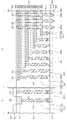
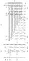
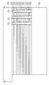
도 6은 본 발명의 다른 실시예에 따른 3차원 반도체 기억 소자를 나타내는 단면도이다.6 is a cross-sectional view showing a three-dimensional semiconductor memory device according to another embodiment of the present invention.
도 6을 참조하면, 기판(500)은 셀 영역(10) 및 주변회로 영역(20)을 포함할 수 있다. 상기 셀 영역(10)의 기판(500) 상에 적층 구조체(515)가 배치될 수 있다. 상기 적층 구조체(515)는 교대로 그리고 반복적으로 적층된 절연 패턴들(505) 및 게이트 패턴(510)을 포함할 수 있다. 수직형 활성 패턴들(530)이 적층 구조체(515)를 관통할 수 있다. 상기 수직형 활성 패턴(530)은 상기 기판(100)에 접속될 수 있다. 데이터 유전막(525)이 상기 각 수직형 활성 패턴(530)의 측벽, 및 상기 각 게이트 패턴(510) 사이에 개재될 수 있다. 상기 적층된 게이트 패턴들(510)은 계단식 구조의 패드부들(512)을 갖는다. 상기 패드부들(512)은 상기 수직형 활성 패턴들(530)의 일측에 배치될 수 있다. 상기 기판(500)은 도 1의 기판(100)과 동일한 물질로 형성될 수 있다. 상기 절연 패턴(505), 게이트 패턴(510), 수직형 활성 패턴(530), 및 데이터 유전막(525)은 각각 도 1의 제1 절연 패턴(105), 제1 게이트 패턴(110), 제1 수직형 활성 패턴(130) 및 제1 데이터 유전막(125)과 동일한 물질로 형성될 수 있다. 상기 수직형 활성 패턴(530)은 도 2a의 수직형 활성 패턴(130a)과 같은 형태로 구현될 수 있다. 상기 데이터 유전막(525)은 도 2b의 데이터 유전막(125a) 또는 도 2c의 데이터 유전막(125b)의 형태로 구현될 수 있다.Referring to FIG. 6, a
상기 주변회로 영역(20)의 기판(500) 상에 주변 게이트(535)가 배치될 수 있다. 주변 게이트 유전막(537)이 상기 주변 게이트(535) 및 기판(500) 사이에 개재될 수 있다. 상기 주변 게이트(535) 양측의 기판(500) 내에 주변 소오스/드레인(540)이 배치될 수 있다. 상기 주변 게이트(535)는 도핑된 반도체(ex, 도핑된 실리콘 등), 도전성 금속 질화물(ex, 질화 티타늄, 질화 탄탈늄), 금속(ex, 텅스텐, 알루미늄 등), 전이 금속(ex, 티타늄, 또는 탄탈늄 등), 또는 금속-반도체 화합물(ex, 금속 실리사이드 등) 등에서 적어도 하나를 포함할 수 있다. 상기 주변 게이트 유전막(537)은 산화물, 질화물, 산화질화물 및/또는 고유전물 등을 포함할 수 있다.A
상기 기판(500) 전면 상에 층간 유전막(545)이 배치될 수 있다. 상기 층간 유전막(545)은 상기 적층 구조체(515) 및 주변 트랜지스터를 덮는다. 상기 층간 유전막(545)의 상부면은 상기 적층 구조체(515)의 최상면 보다 높을 수 있다. 상기 층간 유전막(545)은 단일층(single-layered) 또는 다층(multi-layered)일 수 있다. 상기 층간 유전막(545)은 산화물, 질화물 및/또는 산화질화물 등을 포함할 수 있다.An
제1 콘택 구조체들(580)이 상기 셀 영역(10)내 층간 유전막(545)을 관통하여 상기 패드부들(512)에 각각 접속될 수 있다. 제2 콘택 구조체들(582)이 상기 셀 영역(10)내 층간 유전막(545)을 관통하여 상기 수직형 활성 패턴들(530)에 각각 접속될 수 있다. 제3 콘택 구조체들(584)이 상기 주변회로 영역(20)내 층간 유전막(545)을 관통하여 상기 주변 게이트(535) 및 주변 소오스/드레인(540)에 각각 접속될 수 있다.The
상기 패드부들(512)이 계단식 구조를 가짐으로써, 상기 제1 콘택 구조체들(580)의 높이들은 서로 다를 수 있다. 예컨대, 상기 패드부들(512)이 낮아질수록, 상기 제1 콘택 구조체(580)의 높이들은 증가될 수 있다. 상기 각 제1 콘택 구조체(580)는 상기 층간 유전막(545)을 관통하는 제1 콘택홀(550) 내에 배치될 수 있다. 상기 제1 콘택 구조체(580)는 상기 제1 콘택홀(550) 내에서 차례로 적층된 제1 콘택부(560a) 및 제2 콘택부(575a)를 포함할 수 있다. 이때, 상기 제2 콘택부(575a)의 상부면의 폭은 상기 제1 콘택부(560a)의 상부면의 폭 보다 작은 것이 바람직하다. 물론, 상기 제2 콘택부(575a)의 하부면의 폭도 상기 제1 콘택부(560a)의 상부면의 폭 보다 작다. 상기 제1 콘택부(560a)의 상부면은 상기 층간 유전막(545)의 상부면 보다 낮은 레벨에 위치할 수 있다. 상기 제2 콘택부(575a)의 상부면은 상기 층간 유전막(545)의 상부면과 실질적으로 동일한 레벨에 위치할 수 있다. 절연 스페이서(570a)가 상기 제1 콘택홀(550)의 상부측벽 및 상기 제2 콘택부(575a) 사이에 개재될 수 있다. 상기 절연 스페이서(570a)는 상기 제1 콘택부(560a)의 상부면의 가장자리 상에 배치될 수 있으며, 상기 제2 콘택부(575a)는 상기 제1 콘택부(560a)의 상부면의 중앙부 상에 배치될 수 있다.Since the
상기 절연 스페이서(570a)는 산화물, 질화물 및/또는 산화질화물 등을 포함할 수 있다. 상기 제1 콘택부(560a)은 도핑된 반도체(ex, 도핑된 실리콘), 금속(ex, 텅스텐, 알루미늄, 구리 등), 전이 금속(ex, 티타늄, 탄탈늄 등), 도전성 금속 질화물(ex, 질화티타늄, 질화 탄탈늄 등), 또는 금속-반도체 화합물(ex, 금속 실리사이드 등) 등에서 적어도 하나를 포함할 수 있다. 상기 제2 콘택부(575a)는 도핑된 반도체(ex, 도핑된 실리콘), 금속(ex, 텅스텐, 알루미늄, 구리 등), 전이 금속(ex, 티타늄, 탄탈늄 등), 도전성 금속 질화물(ex, 질화티타늄, 질화 탄탈늄 등), 또는 금속-반도체 화합물(ex, 금속 실리사이드 등) 등에서 적어도 하나를 포함할 수 있다. 상기 제2 콘택부(575a)는 상기 제1 콘택부(560a)와 동일한 도전 물질로 형성될 수 있다. 이와는 다르게, 상기 제2 콘택부(575a)는 상기 제2 콘택부(560a)와 다른 도전 물질을 포함할 수 있다.The insulating
일 실시예에 따르면, 상기 제1 콘택부(560a)는 필라 형태(pillar-shaped)일 수 있다. 또한, 상기 제2 콘택부(575a)는 필라 형태일 수 있다.According to one embodiment, the
상기 각 제2 콘택 구조체(582)는 상기 층간 유전막(545)을 관통하는 제2 콘택홀(552) 내에 배치될 수 있다. 상기 제2 콘택 구조체(582)는 상기 제2 콘택홀(552) 내에 차례로 적층된 제1 콘택부(563a) 및 제2 콘택부(575b)를 포함할 수 있다. 상기 제2 콘택 구조체(582)의 제2 콘택부(575b)의 상부면의 폭은 상기 제1 콘택부(563a)의 상부면의 폭 보다 작을 수 있다. 상기 절연 스페이서(570a)가 상기 제2 콘택 구조체(582)의 제2 콘택부(575b)와 상기 제2 콘택홀(552)의 상부측벽 사이에 개재될 수 있다. 상기 제2 콘택 구조체(582)의 제1 콘택부(563a) 및 제2 콘택부(575b)는 각각 상기 제1 콘택 구조체(580)의 제1 콘택부(560a) 및 제2 콘택부(575a)과 동일한 도전 물질로 형성될 수 있다. 일 실시예에 따르면, 상기 제2 콘택 구조체(582)의 제2 콘택부(575b)의 상부면은 상기 제1 콘택 구조체(580)의 제2 콘택부(575a)의 상부면과 실질적으로 동일한 레벨에 위치할 수 있다. 하지만, 본 발명은 여기에 한정되지 않는다.Each of the
상기 각 제3 콘택 구조체(584)는 상기 주변회로 영역(20) 내 층간 유전막(545)을 관통하는 제3 콘택홀(554) 내에 배치될 수 있다. 상기 제3 콘택 구조체(584)는 상기 제3 콘택홀(554) 내에 차례로 적층된 제1 콘택부(565a) 및 제2 콘택부(575c)를 포함할 수 있다. 상기 제3 콘택 구조체(584)의 제2 콘택부(575c)의 상부면의 폭은 상기 제1 콘택부(565a)의 상부면의 폭 보다 작을 수 있다. 상기 절연 스페이서(570a)가 상기 제3 콘택 구조체(584)의 제2 콘택부(575c)와 상기 제3 콘택홀(554)의 상부측벽 사이에 개재될 수 있다. 상기 제3 콘택 구조체(584)의 제1 콘택부(565a) 및 제2 콘택부(575c)는 각각 상기 제1 콘택 구조체(580)의 제1 콘택부(560a) 및 제2 콘택부(575a)와 동일한 도전 물질로 형성될 수 있다. 상기 제3 콘택 구조체(584)의 제2 콘택부(575c)의 상부면은 상기 제1 콘택 구조체(580)의 제2 콘택부(575a)의 상부면과 실질적으로 동일한 레벨에 위치할 수 있다.Each of the
상기 셀 영역(10) 내 상기 층간 유전막(545) 상에 제1 배선들(590a) 및 제2 배선들(590b)이 배치될 수 있다. 상기 제1 배선들(590a)은 상기 제1 콘택 구조체들(580)의 제2 콘택부들(575a)에 각각 접속될 수 있다. 상기 제2 배선들(590b)은 상기 제2 콘택 구조체들(582)의 제2 콘택부들(575b)에 각각 접속될 수 있다. 일 실시예에 따르면, 상기 제2 배선들(590b)은 비트 라인들에 해당할 수 있다. 제3 배선들(590c)이 상기 주변회로 영역(20)내 층간 유전막(545) 상에 배치될 수 있다. 상기 제3 배선들(590c)은 상기 제3 콘택 구조체들(584)의 제2 콘택부들(575c)에 각각 접속될 수 있다. 상기 배선들(590a, 590b, 590c)는 금속(ex, 텅스텐, 알루미늄, 구리 등), 전이 금속(ex, 티타늄, 탄탈늄 등) 또는 도전성 금속 질화물(ex, 질화 티타늄, 질화 탄탈늄 등) 등에서 적어도 하나를 포함할 수 있다.
상술된 3차원 반도체 기억 소자에 따르면, 상기 제1 콘택 구조체(580)는 하나의 상기 제1 콘택홀(550) 내에 차례로 적층된 상기 제1 콘택부(560a) 및 제2 콘택부(575a)를 포함할 수 있다. 이때, 상기 제2 콘택부(575a)의 상부면의 폭은 상기 제1 콘택부(560a)의 상부면의 폭 보다 작다. 이로 인하여, 상기 제2 콘택부들(575a)과 접속되는 제1 배선들(590a)의 선폭들 및/또는 간격을 감소시킬 수 있다. 이로 인하여, 고집적화에 최적화된 3차원 반도체 기억 소자를 구현할 수 있다. 또한, 상기 절연 스페이서(570a)를 이용하여 상기 제2 콘택부(575a)를 형성함으로써, 상기 제2 콘택부(575a)는 상기 제1 콘택부(560a)에 자기 정렬될 수 있다. 이로써, 상기 제1 및 제2 콘택부들(560a, 575a)는 정렬이 요구되지 않는다. 그 결과, 제조 공정의 공정 마진을 향상될 수 있으며, 또한, 우수한 신뢰성을 갖는 3차원 반도체 기억 소자를 구현할 수 있다.According to the above-described three-dimensional semiconductor memory device, the
다음으로, 본 실시예에 따른 3차원 반도체 기억 소자들의 변형예들을 도면들을 참조하여 설명한다.Next, modifications of the three-dimensional semiconductor memory elements according to the present embodiment will be described with reference to the drawings.
도 7a는 본 발명의 다른 실시예에 따른 3차원 반도체 기억 소자의 일 변형예를 나타내는 단면도이다.7A is a cross-sectional view showing a modified example of a three-dimensional semiconductor memory device according to another embodiment of the present invention.
도 7a를 참조하면, 제1 콘택 구조체들(580a)이 층간 유전막(545)을 관통하여 게이트 패턴들(510)의 패드부들(512)에 각각 접속될 수 있다. 상기 각 제1 콘택 구조체(580a)는 층간 유전막(545)을 관통하는 제1 콘택홀(550) 내에 배치될 수 있다. 상기 제1 콘택 구조체(580a)는 차례로 적층된 제1 콘택부(577a) 및 제2 콘택부(558a)를 포함할 수 있다. 상기 제2 콘택부(578a)의 상부면의 폭은 상기 제1 콘택부(577a)의 상부면의 폭 보다 작으며, 절연 스페이서(570a)가 상기 제1 콘택홀(550)의 상부측벽 및 상기 제2 콘택부(578a) 사이에 배치된다. 이때, 상기 제1 콘택부(577a) 내부에 공극(AG)이 배치될 수 있다. 상기 제1 및 제2 콘택부들(577a, 578a)은 서로 동일한 도전 물질로 형성될 수 있다. 상기 제1 및 제2 콘택부들(577a, 578a)은 도 6의 제2 콘택부(575a)와 동일한 물질로 형성될 수 있다.Referring to FIG. 7A, the
이와 마찬가지로, 제2 콘택 구조체들(582a)가 상기 층간 유전막(545)을 관통하여 수직형 활성 패턴들(530) 상에 각각 접속될 수 있다. 상기 각 제2 콘택 구조체(582a)는 상기 층간 유전막(545)을 관통하는 제2 콘택홀(552) 내에 차례로 적층된 제1 콘택부(577b) 및 제2 콘택부(578b)를 포함할 수 있다. 상기 제2 콘택 구조체(582a)의 제2 콘택부(578b)의 상부면의 폭은 상기 제1 콘택부(577b)의 폭 보다 작을 수 있으며, 상기 절연 스페이서(570a)가 상기 제2 콘택부(578b) 및 제2 콘택홀(552)의 상부측벽 사이에 개재될 수 있다. 상기 제2 콘택 구조체(582a)의 제1 콘택부(578a) 내에도 공극(AG)이 형성될 수 있다.Likewise, the
제3 콘택 구조체(584a)들이 주변회로 영역(20)내 층간 유전막(545)을 관통하여 주변 게이트(535) 및 주변 소오스/드레인(540)에 각각 접속될 수 있다. 상기 제3 콘택 구조체(584a)는 상기 층간 유전막(545)을 관통하는 제3 콘택홀(554) 내에 차례로 적층된 제1 콘택부(577c) 및 제2 콘택부(578c)를 포함할 수 있다. 상기 제3 콘택 구조체(584a)의 제1 콘택부(577c) 내에도 공극(AG)이 형성될 수 있다. 상기 제2 및 제3 콘택 구조체들(582a, 584a)의 콘택부들(577b, 577c, 578b, 578c)은 상기 제1 콘택 구조체(580a)의 콘택부들(577a, 578a)과 동일한 물질로 형성될 수 있다.The
도 7b는 본 발명의 다른 실시예에 따른 3차원 반도체 기억 소자의 다른 변형예를 나타내는 단면도이다.7B is a cross-sectional view showing another modification of the three-dimensional semiconductor memory element according to another embodiment of the present invention.
도 7b를 참조하면, 본 변형예에 따르면, 셀 영역(10)의 기판 상에 제1 적층 구조체(515a) 및 제2 적층 구조체(515b)가 차례로 적층될 수 있다. 상기 제1 적층 구조체(515a)는 교대로 그리고 반복적으로 적층된 제1 절연 패턴들(505a) 및 제1 게이트 패턴들(510a)을 포함할 수 있으며, 상기 제2 적층 구조체(515b)는 교대로 그리고 반복적으로 적층된 제2 절연 패턴들(505b) 및 제2 게이트패턴들(510b)을 포함할 수 있다. 제1 수직형 활성 패턴들(530a)이 상기 제1 적층 구조체(515a)를 관통하고, 제2 수직형 활성 패턴들(530b)이 상기 제2 적층 구조체(515b)를 관통하여 상기 제1 수직형 활성 패턴들(530a) 상에 각각 접속될 수 있다. 제1 데이터 유전막(525a)이 상기 제1 수직형 활성 패턴(530a)의 측벽 및 상기 각 제1 게이트 패턴(510a) 사이에 개재될 수 있으며, 제2 데이터 유전막(525b)이 상기 제2 수직형 활성 패턴(530b)의 측벽 및 상기 제2 게이트 패턴(510b) 사이에 개재될 수 있다. 상기 제1 게이트 패터들(510a) 및 제2 게이트 패턴들(510b)은 계단식 구조의 패드부들(512a, 512b)을 포함한다. 상기 구성들은 도 6에 대응되는 구성들과 동일한 물질로 형성될 수 있다.Referring to FIG. 7B, according to this modification, the first
하부 평탄화된 유전막(243)이 상기 제1 게이트 패턴들(510a)의 패드부들(512a) 상에 배치될 수 있다. 또한, 상기 하부 평탄화된 유전막(243)은 주변회로 영역(20) 내 주변 게이트(535) 및 주변 소오스/드레인(540)을 포함하는 기판(500) 상에도 배치될 수 있다. 상기 하부 평탄화된 유전막(243)은 상기 제1 수직형 활성 패턴들(530a)의 상부면들과 실질적으로 동일한 레벨에 위치할 수 있다. 층간 유전막(245)이 상기 하부 평탄화된 유전막(243)을 포함한 기판(500) 전면 상에 배치될 수 있다.The lower
제1 콘택 구조체들(580b, 580)이 상기 제1 게이트 패턴들(510a)의 패드부들(512a) 및 제2 게이트 패턴들(510b)의 패드부들(512b)에 각각 접속될 수 있다. 상기 제1 콘택 구조체들 중에서, 상기 제2 게이트 패턴들(510b)의 패드부들(512b)에 접속되는 제1 콘택 구조체들(580)의 각각은 상기 층간 유전막(545)을 관통하는 제1 콘택홀(550) 내에 차례로 적층된 제1 콘택부(560a) 및 제2 콘택부(575a)를 포함할 수 있다. 상기 제2 게이트 패턴(510b)의 패드부(512b)에 접속된 제1 콘택 구조체(580)는 상기 제1 콘택부(560a)가 상기 패드부(512b)에 직접 접촉될 수 있다.The
이와는 다르게, 상기 제1 게이트 패턴들(510a)의 패드부들(512a) 중에서 적어도 일부(some)에 접속되는 제1 콘택 구조체들(580b)는 차례로 적층된 제1 하부 콘택 플러그(615), 제1 콘택부(560a) 및 제2 콘택부(575a)를 포함할 수 있다. 상기 제1 하부 콘택 플러그(615)는 상기 하부 평탄화된 유전막(243)을 관통하는 제1 하부홀(610) 내에 배치되어, 상기 제1 게이트 패턴(510a)의 패드부(512a)에 연결될 수 있다. 상기 제1 게이트 패턴(510a)의 패드부(512a)에 연결된 제1 콘택 구조체들(580b)의 제1 및 제2 콘택부들(560a, 575a)은 상기 층간 유전막(545)을 관통하는 제1 콘택홀(550)내 및 상기 제1 하부 콘택 플러그(615) 상에 차례로 적층될 수 있다. 일 실시예에 따르면, 상기 제1 게이트 패턴(510a)의 패드부(512a)에 연결된 제1 콘택 구조체(580b)의 제1 콘택부(560a)의 하부면은 상기 제1 하부 콘택 플러그(615)의 상부면 보다 좁은 폭을 가질 수 있다.Alternatively, the
제3 콘택 구조체들(584b)이 상기 주변 게이트(535) 및 주변 소오스/드레인(540)에 각각 연결될 수 있다. 상기 각 제3 콘택 구조체(584b)는 차례로 적층된 제2 하부 콘택 플러그(617), 제1 콘택부(565a) 및 제2 콘택부(575c)를 포함할 수 있다. 상기 제2 하부 콘택 플러그(617)는 상기 주변회로 영역(20) 내 하부 평탄화된 유전막(243)을 관통하는 제2 하부홀(612) 내에 배치될 수 있다. 일 실시예에 따르면, 상기 제3 콘택 구조체(584b)의 제1 콘택부(565a)의 하부면의 폭은 상기 제2 하부 콘택 플러그(617)의 하부면의 폭 보다 작을 수 있다.
일 실시예에 따르면, 최상위의 제1 게이트 패턴의 패드부에 연결된 제1 콘택 구조체(580)의 제1 콘택부(560a)는 패드부에 직접 접속될 수 있다. 상기 하부 콘택 플러그들(615, 617)은 도핑된 반도체(ex, 도핑된 실리콘 등), 금속(ex, 텅스텐, 알루미늄 등), 전이 금속(ex, 티타늄, 탄탈늄 등), 도전성 금속 질화물(ex, 질화 티타늄, 질화 탄탈늄 등), 또는 금속-반도체 화합물(ex, 금속 실리사이드 등) 등에서 적어도 하나를 포함할 수 있다.According to one embodiment, the
도 7c는 본 발명의 다른 실시예에 따른 3차원 반도체 기억 소자의 또 다른 변형예를 나타내는 단면도이다.7C is a cross-sectional view showing still another modification of the three-dimensional semiconductor memory element according to another embodiment of the present invention.
도 7c를 참조하면, 제1 게이트 패턴들(510a)의 패드부들(512b) 중에서 일부(some)와 접속된 제1 콘택 구조체(580c)는 차례로 적층된 제1 하부 콘택 플러그(576a), 제1 콘택부(577a) 및 제2 콘택부(578a)를 포함할 수 있다. 상기 제1 하부 콘택 플러그(576a)는 하부 평탄화된 유전막(243)을 관통하는 제1 하부홀(610) 내에 배치될 수 있다. 이때, 상기 제1 콘택 구조체(580c)의 제1 하부 콘택 플러그(576a) 및 제1 콘택부(577a)의 각각의 내부에 공극(AG)이 형성될 수 있다. 상기 제1 하부 콘택 플러그(576a), 제1 콘택부(577a) 및 제2 콘택부(578a)는 동일한 도전 물질로 형성될 수 있다.Referring to FIG. 7C, the
이와 유사하게, 주변회로 영역(20) 내의 제3 콘택 구조체(584c)는 차례로 적층된 제2 하부 콘택 플러그(576b), 제1 콘택부(577c) 및 제2 콘택부(578c)를 포함할 수 있다. 상기 제2 하부 콘택 플러그(576b)는 상기 주변회로 영역(20) 내 하부 평탄화된 유전막(243)을 관통하는 제2 하부홀(612) 내에 배치될 수 있다. 상기 제3 콘택 구조체(584c)의 제2 하부 콘택 플러그(576b) 및 제1 콘택부(577c)의 각각 내부에 공극(AG)이 형성될 수 있다. 제2 하부 콘택 플러그(576b)은 제1 및 제2 콘택부들(577c, 578c)와 동일한 물질로 형성될 수 있다.Similarly, the
도 7d는 본 발명의 다른 실시예에 따른 3차원 반도체 기억 소자의 또 다른 변형예를 나타내는 단면도이다.7D is a cross-sectional view showing still another modification of the three-dimensional semiconductor memory element according to another embodiment of the present invention.
도 7d를 참조하면, 본 변형예에 따르면, 패드부(512)에 전기적으로 접속된 제1 배선(590a)과 수직형 활성 패턴(530)의 상단에 전기적으로 접속된 제2 배선(590b')이 서로 다른 레벨에 위치할 수 있다. 예컨대, 상부 유전막(593)이 층간 유전막(545) 및 제1 및 제3 배선들(590a, 590b) 상에 배치될 수 있다. 상기 제2 배선(590b')과 연결된 제2 콘택 구조체(650)는 상기 셀 영역(10)의 상부 유전막(593) 및 층간 유전막(545)을 관통하는 제2 콘택홀(552a) 내에 배치되어, 상기 수직형 활성 패턴(530)과 접속될 수 있다.7D, according to this modification, the
상기 제2 콘택 구조체(650)는 상기 제2 콘택홀(552a) 내에 차례로 적층된 제1 콘택부(640) 및 제2 콘택부(645)를 포함할 수 있다. 상기 제2 콘택부(645)의 상부면의 폭은 상기 제1 콘택부(640)의 상부면의 폭 보다 작을 수 있다. 제2 절연 스페이서(595)가 상기 제2 콘택부(645) 및 제2 콘택홀(552a)의 상부측벽 사이에 개재될 수 있다. 제2 콘택부(645)는 상기 상부 유전막(593)의 상부면과 실질적으로 동일한 레벨에 위치할 수 있다. 상기 제2 배선(590')이 상기 상부 유전막(593) 상에 배치되어 상기 제2 콘택 구조체(650)의 제2 콘택부(645)와 접속될 수 있다.The
본 변형예에 따르면, 상기 제2 배선(590b')이 상기 제1 배선(590a) 보다 높은 레벨에 위치할 수 있다. 하지만, 본 발명은 여기에 한정되지 않는다. 상기 제1 배선(590a)이 상기 제2 배선(590b') 보다 높은 레벨에 위치할 수도 있다.According to this modification, the
한편, 본 실시예에 따른 기술적 사상은 상술된 제1 실시예에 적용될 수 있다. 이를 도면을 참조하여 설명한다. 본 변형예에서 상술된 구성요소들과 동일한 구성요소들은 동일한 참조부호를 사용한다.On the other hand, the technical idea according to the present embodiment can be applied to the first embodiment described above. This will be described with reference to the drawings. The same components as those described above in this modification use the same reference numerals.
도 7e는 본 발명의 다른 실시예에 따른 3차원 반도체 기억 소자의 또 다른 변형예를 나타내는 단면도이다.7E is a cross-sectional view showing still another modification of the three-dimensional semiconductor memory element according to another embodiment of the present invention.
도 7e를 참조하면, 제4 적층 구조체(415) 및 제4 평탄화된 유전막(435) 상에 상부 유전막(450)이 배치될 수 있다. 제1, 제2, 제3 및 제4 평탄화된 유전막들(135, 235, 335, 435) 및 상부 유전막(450)은 층간 유전막(470)에 포함될 수 있다.Referring to FIG. 7E, the
제1 콘택 구조체들(580)이 상기 층간 유전막(470)을 관통하여 상기 게이트 패턴들(110, 210, 310, 410)의 패드부들(112, 212, 312, 412)에 각각 접속될 수 있다. 상기 각 제1 콘택 구조체(580)는 상기 층간 유전막(470)을 관통하는 제1 콘택홀(550) 내에 배치될 수 있다. 상기 제1 콘택 구조체(580)는 상기 제1 콘택홀(550) 내에 차례로 적층된 제1 콘택부(560a) 및 제2 콘택부(575a)를 포함할 수 있다. 도 6에서 상술된 바와 같이, 상기 제2 콘택부(575a)의 상부면의 폭은 상기 제1 콘택부(560a)의 상부면의 폭 보다 작을 수 있다. 절연 스페이서(570a)가 제2 콘택부(575a)와 제1 콘택홀(550)의 상부측벽 사이에 개재될 수 있다.The
제2 콘택 구조체들(582)이 상기 층간 유전막(470)을 관통하여 제4 수직형 활성 패턴들(430) 상에 각각 접속될 수 있다. 상기 제2 콘택 구조체(582)는 도 6을 참조하여 설명한 구조와 동일할 수 있다. 상기 제1 콘택 구조체(580)에 연결된 제1 배선(590a) 및 제2 콘택 구조체(582)에 연결된 제2 배선(590b)이 상기 층간 유전막(470) 상에 배치될 수 있다.The
본 변형예에서, 상기 제1 콘택 구조체(580)는 도 7a, 도 7b 또는 도 7c에 개시된 제1 콘택 구조체(580a, 580b 또는 580c)와 대체될 수 있다. 상기 제2 콘택 구조체(582)는 도 7d를 참조하여 설명한 것과 같은 형태들로 구현될 수도 있다.In this variation, the
도 8a 내지 도 8c는 본 발명의 다른 실시예에 따른 3차원 반도체 기억 소자의 제조 방법을 설명하기 위한 단면도들이다.8A to 8C are cross-sectional views illustrating a method of manufacturing a three-dimensional semiconductor memory device according to another embodiment of the present invention.
도 8a를 참조하면, 셀 영역(10) 및 주변회로 영역(20)을 포함하는 기판(500)을 준비한다. 상기 셀 영역(10)의 기판(500) 상에 적층 구조체(515)를 형성할 수 있다. 상기 적층 구조체(515)는 교대로 그리고 반복적으로 적층된 절연 패턴들(505) 및 게이트 패턴들(515)을 포함할 수 있다. 상기 적층 구조체(515)를 관통하는 수직형 활성 패턴들(530)를 형성할 수 있다. 상기 수직형 활성 패턴(530)과 상기 각 게이트 패턴(510) 사이의 데이터 유전막(525)을 형성할 수 있다. 상기 적층된 게이트 패턴들(510)이 계단식 구조의 패드부들(512)를 갖도록 형성할 수 있다. 일 실시예에 따르면, 상기 수직형 활성 패턴들(530)을 형성한 후에, 상기 계단식 구조의 패드부들(512)를 형성할 수 있다. 하지만, 본 발명은 여기에 한정되지 않는다.Referring to FIG. 8A, a
상기 주변회로 영역(20)의 기판(500) 상에 주변 게이트 유전막(537) 및 주변 게이트(535)를 차례로 형성하고, 상기 주변 게이트(535) 양측의 기판(500) 내에 주변 소오스/드레인(540)을 형성할 수 있다.A peripheral
이어서, 상기 기판(500) 전면 상에 층간 유전막(545)을 형성할 수 있다. 상기 층간 유전막(545)을 관통하는 제1 콘택홀들(550), 제2 콘택홀들(552) 및 제4 콘택홀들(554)를 형성할 수 있다. 상기 제1 콘택홀들(550)은 상기 패드부들(512)를 각각 노출시킬 수 있다. 상기 제2 콘택홀들(552)은 상기 수직형 활성 패턴들(530)을 각각 노출시킬 수 있다. 상기 제3 콘택홀들(554)은 상기 주변 게이트(535) 및 주변 소오스/드레인(540)을 각각 노출시킬 수 있다.Then, an
상기 기판(500) 상에 상기 콘택홀들(550, 552, 554)를 채우는 제1 도전막을 형성할 수 있다. 상기 제1 도전막을 상기 층간 유전막(545)이 노출될 때까지 평탄화시키어, 상기 제1 콘택홀(550)내의 제1 콘택 플러그(560), 상기 제2 콘택홀(552)내의 제2 콘택 플러그(563), 및 상기 제3 콘택홀(554)내의 제3 콘택 플러그(565)를 형성할 수 있다.A first conductive layer filling the contact holes 550, 552, and 554 may be formed on the
도 8b를 참조하면, 상기 제1, 제2 및 제3 콘택 플러그들(560, 563, 565)의 상부면들을 리세스한다. 상기 리세스된 제1, 제2 및 제3 콘택 플러그들(560a, 563a, 565a)의 상부면들은 상기 층간 유전막(545)의 상부면 보다 낮은 레벨에 위치할 수 있다. 이에 따라, 상기 리세스된 콘택 플러그들(560a, 563a, 565a)의 상부면들 위의 콘택홀들(550, 552, 554)의 윗부분들이 빈 상태들일 수 있다.Referring to FIG. 8B, upper surfaces of the first, second, and third contact plugs 560, 563, and 565 are recessed. The top surfaces of the recessed first, second and third contact plugs 560a, 563a, and 565a may be located at a lower level than the top surface of the
이어서, 상기 기판(500) 전면 상에 스페이서막(570)을 콘포말하게 형성할 수 있다. 상기 스페이서막(570)은 산화막, 질화막 및/또는 산화질화막 등으로 형성될 수 있다.Then, a
도 8c를 참조하면, 상기 리세스된 콘택 플러그들(560a, 563a, 565a)이 노출될 때까지 상기 스페이서막(570)을 전면 이방성 식각할 수 있다. 이로써, 절연 스페이서들(570a)이 상기 리세스된 콘택 플러그들(560a, 563a, 565a)의 상부면 위의 상기 콘택홀들(550, 552, 554)의 상부측벽들 상에 각각 형성될 수 있다.Referring to FIG. 8C, the
이어서, 상기 스페이서들(570a)를 갖는 기판(500) 상에 상기 콘택홀들(550, 552, 554)을 채우는 제2 도전막(575)을 형성할 수 있다. 상기 제2 도전막(575)은 상기 노출된 상기 리세스된 콘택 플러그들(560a, 563a, 565a)과 접촉된다.Next, a second
상기 제2 도전막(575)을 상기 층간 유전막(545)이 노출될 때까지 평탄화시키어, 도 6의 제1, 제2 및 제3 콘택 구조체들(580, 582, 584)을 형성할 수 있다. 이어서, 도 6의 제1, 제2 및 제3 배선들(590a, 590b, 590c)을 형성하여, 도 6의 3차원 반도체 기억 소자를 구현할 수 있다.The second
상술된 3차원 반도체 기억 소자의 제조 방법에 따르면, 좁은 상부면의 폭을 갖는 제2 콘택부들(575a, 575b, 575c)은 상기 절연 스페이서들(570a)를 이용하여 상기 제1 콘택부들(560a, 563a, 565a)이 내부에 형성된 콘택홀들(550, 552, 554) 내에 각각 형성될 수 있다. 이에 따라, 상기 제2 콘택부들(575a, 575b, 575c)은 각각 상기 제1 콘택부들(560a, 563a, 565a)에 자기 정렬적으로 형성될 수 있다. 이에 따라, 포토리소그라피 공정의 횟수를 감소시킬 수 있으며, 또한, 상기 제1 및 제2 콘택부들은 정렬로부터 자유롭다. 결과적으로, 제조 공정을 단순화시켜 3차원 반도체 기억 소자의 생산성을 향상시킬 수 있으며, 또한, 우수한 신뢰성을 갖고, 고도로 집적화된 3차원 반도체 기억 소자를 구현할 수 있다.According to the above-described method for manufacturing a three-dimensional semiconductor memory device, the
다음으로, 도 7a에 개시된 3차원 반도체 기억 소자의 제조 방법을 도면들을 참조하여 설명한다.Next, a method of manufacturing the three-dimensional semiconductor memory element shown in Fig. 7A will be described with reference to the drawings.
도 9a 내지 도 9c는 본 발명의 다른 실시예에 따른 3차원 반도체 기억 소자의 제조 방법의 일 변형예를 설명하기 위한 단면도들이다.9A to 9C are cross-sectional views for explaining a modified example of a method of manufacturing a three-dimensional semiconductor memory device according to another embodiment of the present invention.
도 9a를 참조하면, 콘택홀들(550, 552, 554)의 형성까지의 제조 방법은 도 8a를 참조하여 설명한 것과 동일할 수 있다. 상기 콘택홀들(550, 552, 554)을 채우는 희생막을 기판(500) 전면 상에 형성할 수 있다. 상기 희생막은 상기 층간 유전막(545)에 대하여 식각선택비를 갖는 물질로 형성할 수 있다.Referring to FIG. 9A, a manufacturing method up to the formation of the contact holes 550, 552, and 554 may be the same as that described with reference to FIG. 8A. A sacrificial layer filling the contact holes 550, 552, and 554 may be formed on the entire surface of the
이어서, 상기 희생막을 상기 층간 유전막(545)이 노출될 때까지 평탄화시켜 상기 콘택홀(550, 552, 554)을 각각 채우는 희생 플러그들을 형성할 수 있다. 이어서, 상기 희생 플러그들을 리세스할 수 있다. 상기 리세스된 희생 플러그들(600, 603, 605)의 상부면들은 상기 층간 유전막(545)의 상부면 보다 낮은 레벨에 위치한다. 이어서, 상기 기판(500) 전면 상에 스페이서막을 콘포말하게 형성하고, 상기 스페이서막을 상기 리세스된 희생 플러그들(600, 603, 605)이 노출될 때까지 전면 이방성 식각한다. 이로써, 상기 리세스된 희생 플러그들(600, 603, 605) 상에 절연 스페이서들(570a)이 형성될 수 있다.The sacrificial layer may then be planarized until the
상기 리세스된 희생 플러그들(600, 603, 605)는 상기 절연 스페이서(570a)에 대해서도 식각선택비를 갖는 물질로 형성될 수 있다. 예를 들면, 상기 층간 유전막(545) 및 절연 스페이서(570a)가 산화물로 형성되는 경우에, 상기 희생 플러그들(600, 603, 605)은 폴리실리콘, SiC, SiOC, SiOCH, SiN, SiON, 또는 탄소를 함유하는 SOH(Spin On Hardmask) 등에서 적어도 하나를 포함할 수 있다.The recessed
도 9b를 참조하면, 상기 노출된 희생 플러그들(600, 603, 605)를 제거할 수 있다. 이때, 상기 절연 스페이서들(570a)은 잔존된다.Referring to FIG. 9B, the exposed
도 9c를 참조하면, 이어서, 상기 희생 플러그들(600, 603, 605)이 제거된 콘택홀들(550, 552, 554)을 갖는 기판(500) 상에 도전막(578)을 형성할 수 있다. 상기 도전막(578)은 콘포말하게 형성될 수 있다. 이에 따라, 상기 도전막(578)은 상기 절연 스페이서(570a) 아래의 상기 각 콘택홀(550, 552 또는 554)의 내벽을 따라 콘포말하게 형성될 수 있다. 상기 각 절연 스페이서(570a)로 둘러싸인 공간은 상기 각 절연 스페이서(570a) 아래의 상기 각 콘택홀(550, 552 또는 554)의 폭 보다 작다. 이에 따라, 상기 각 절연 스페이서(570a)의 의해 둘러싸인 공간이 상기 도전막(578)으로 채워지기 전에, 상기 각 절연 스페이서(570a) 아래의 상기 각 콘택홀(550, 552 또는 554)의 내벽 상에 상기 도전막(578)이 콘포말하게 형성될 수 있다. 상기 각 절연 스페이서(570a)의 의해 둘러싸인 공간이 상기 도전막(578)으로 채워진 후에는, 상기 각 절연 스페이서(570a) 아래의 각 콘택홀(550, 552 또는 554) 내부에 상기 도전막(578)이 공급되지 않을 수 있다. 이에 따라, 상기 각 절연 스페이서(570a) 아래에 위치한 상기 각 콘택홀(550, 552 또는 554) 내에 상기 도전막(578)에 의해 둘러싸인 공극(AG)이 형성될 수 있다.9C, a
이어서, 상기 도전막(578)을 상기 층간 유전막(545)이 노출될 때까지 평탄화시키어, 도 7a의 콘택 구조체들(580a, 582a, 584a)을 형성할 수 있다. 이어서, 도 7a의 배선들(590a, 590b, 590c)를 형성하여, 도 7a에 개시된 3차원 반도체 기억 소자를 구현할 수 있다.The
도 7b에 개시된 3차원 반도체 기억 소자의 제조 방법은 도 7b를 참조하여 설명한다.The method of manufacturing the three-dimensional semiconductor memory element shown in Fig. 7B will be described with reference to Fig. 7B.
도 7b를 참조하면, 도 3a 내지 도 도 3c를 참조하여 설명한 제조 방법들을 적용하여, 제1 적층 구조체(515a), 제1 수직형 활성 패턴들(530a) 및 하부 평탄화된 유전막(243)을 형성할 수 있다.Referring to FIG. 7B, the fabrication methods described with reference to FIGS. 3A to 3C are applied to form a
이어서, 하부 평탄화된 유전막(243)을 관통하는 제1 하부홀들(610) 및 제2 하부홀들(612)을 형성할 수 있다. 상기 제1 하부홀들(610)은 상기 셀 영역(10)내의 제1 게이트 패턴들(510a)의 패드부들(512a)를 노출시킬 수 있으며, 상기 제2 하부홀들(612)은 상기 주변회로 영역(20)내의 주변 게이트(535) 및 주변 소오스/드레인(540)을 노출시킬 수 있다. 이어서, 상기 각 제1 하부홀(610)을 채우는 제1 하부 콘택 플러그(615) 및 상기 각 제2 하부홀(612)을 채우는 제2 하부 콘택 플러그(617)를 형성할 수 있다.Subsequently, first
이어서, 상기 기판(500) 상에 제2 적층 구조체(515b), 제2 수직형 활성 패턴(530) 및 층간 유전막(545)을 형성할 수 있다. 이어서, 도 8a 내지 도 8c를 참조하여 설명한 방법들을 적용하여, 콘택 구조체들(580, 580b, 582, 584)을 형성할 수 있다. 이어서, 배선들(590a, 590b, 590c)을 형성하여 도 7b에 도시된 3차원 반도체 기억 소자를 구현할 수 있다.Next, a second
다음으로, 도 7c에 개시된 3차원 반도체 기억 소자의 제조 방법을 도면들을 참조하여 설명한다.Next, a method of manufacturing the three-dimensional semiconductor memory element shown in FIG. 7C will be described with reference to the drawings.
도 10a 및 도 10b는 본 발명의 다른 실시예에 따른 3차원 반도체 기억 소자의 제조 방법의 다른 변형예를 설명하기 위한 단면도들이다.10A and 10B are cross-sectional views for explaining another modification of the method for fabricating a three-dimensional semiconductor memory device according to another embodiment of the present invention.
도 10a를 참조하면, 도 7b를 참조하여 설명한 방법에서, 제1 및 제2 하부 콘택 플러그들(615, 617)을 대신하여, 제1 및 제2 하부 희생 플러그들(615a, 615b)를 형성할 수 있다.Referring to FIG. 10A, in the method described with reference to FIG. 7B, instead of forming the first and second lower contact plugs 615 and 617, first and second lower
이어서, 제2 적층 구조체(515b), 제2 수직형 활성 패턴들(530b) 및 층간 유전막(545)을 형성한 후에, 도 9a를 참조하여 설명한 것과 같이, 리세스된 희생 플러그들(600, 603, 605) 및 절연 스페이서들(570a)을 형성할 수 있다. 희생 플러그들(600, 603, 605) 중에서 일부(600, 605)는 상기 제1 및 제2 하부 희생 플러그들(615a, 617a)과 접촉될 수 있다. 상기 제1 및 제2 하부 희생 플러그들(615a, 617a)은 상기 희생 플러그들(600, 603, 605)과 동일한 물질로 형성될 수 있다.Subsequently, after forming the
도 10b를 참조하면, 상기 희생 플러그들(600, 603, 605) 및 상기 제1 및 제2 하부 희생 플러그들(615a, 617a)을 제거하여, 상기 절연 스페이서들(570a) 아래의 콘택홀들(550, 552, 554) 및 하부홀들(610, 612)을 비울 수 있다.Referring to FIG. 10B, the sacrifice plugs 600, 603, and 605 and the first and second lower
이어서, 상기 기판(500) 전면 상에 도전막(578)을 콘포말하게 형성할 수 있다. 이에 따라, 도 9c를 참조하여 설명한 바와 같이, 상기 도전막(578)은 상기 절연 스페이서들(570a) 아래의 콘택홀들(550, 552, 554) 및 하부홀들(610, 612)의 내면들을 따라 콘포말하게 형성될 수 있으며, 상기 절연 스페이서들(570a)로 둘러싸인 공간들(즉, 콘택홀들(550, 552, 554)의 일부분들)을 채울 수 있다.Then, a
이어서, 상기 도전막(578)을 평탄화시키어, 도 7c에 개시된 콘택 구조체들(580a, 580c, 582a, 584a)를 형성할 수 있다. 이어서, 배선들(590a, 590b, 590c)을 형성하여 도 7c에 개시된 3차원 반도체 기억 소자를 구현할 수 있다.Then, the
도 7d에 개시된 3차원 반도체 기억 소자의 제조 방법은 도 8a 내지 도 8c를 참조하여 설명한 것과 유사할 수 있다. 다만, 수직형 활성 패턴들(530)과 접속된 제2 콘택 구조체들(582a') 및 제2 배선들(590a')을 제1 배선들(590a)을 형성한 후에 형성할 수 있다.The method of manufacturing the three-dimensional semiconductor memory element shown in Fig. 7D may be similar to that described with reference to Figs. 8A to 8C. However, the
한편, 도 7e에 개시된 3차원 반도체 기억 소자는 상술된 제1 실시예의 제조 방법들 및 상술된 제2 실시예의 제조 방법들을 조합하여 구현할 수 있다.
On the other hand, the three-dimensional semiconductor memory element disclosed in FIG. 7E can be implemented by combining the manufacturing methods of the first embodiment described above and the manufacturing methods of the second embodiment described above.
(제3 실시예)(Third Embodiment)
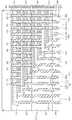
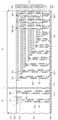
도 11a는 본 발명의 또 다른 실시예에 따른 3차원 반도체 기억 소자를 나타내는 단면도이다.11A is a cross-sectional view showing a three-dimensional semiconductor memory device according to still another embodiment of the present invention.
도 11a를 참조하면, 기판(700) 상에 적층 구조체(715)가 배치될 수 있다. 상기 적층 구조체(715)는 교대로 그리고 반복적으로 적층된 절연 패턴들(705) 및 게이트 패턴들(710)을 포함할 수 있다. 수직형 활성 패턴들(730)이 상기 적층 구조체(715)를 관통할 수 있다. 상기 게이트 패턴들(710)은 계단식 구조를 갖는 패드부들(712)을 포함할 수 있다.Referring to FIG. 11A, a
층간 유전막(740)이 상기 적층 구조체(715)를 포함한 기판(700) 전면 상에 배치될 수 있다. 콘택 플러그들(750)이 상기 층간 유전막(740)을 관통하여 상기 패드부들(712)에 각각 접속될 수 있다. 상기 콘택 플러그들(750)은 일 방향으로 배열될 수 있다. 상기 각 콘택 플러그(750)는 인접한 콘택 플러그와 상기 일 방향으로 콘택-간격(L1, L2, L3, L4 또는 L5)으로 이격될 수 있다. 이때, 상기 콘택-간격들(L1, L2, L3, L4, L5) 중에서 어느 하나는 다른 하나와 다를 수 있다. 상기 일 방향은 도 11a에서 x축 방향에 해당할 수 있다.An
일 실시예에 따르면, 도 11a에 개시된 바와 같이, 상기 콘택-간격들(L1, L2, L3, L4, L5)은 상기 계단식 구조의 패드부들(715)의 내리막 방향(descent direction)으로 점진적으로 감소될 수 있다.According to one embodiment, the contact-spacings L1, L2, L3, L4, and L5 gradually decrease in the descent direction of the
상기 각 패드부(712)는 상기 일 방향으로 소정의 폭(W1, W2, W3, W4 또는 W5)을 가질 수 있다. 상기 각 패드부들(712)의 상기 폭들(W1, W2, W3, W4, W5)은 실질적으로 동일할 수 있다. 이와는 달리, 도 11a에 개시된 바와 같이, 상기 패드부들(712)의 폭들(W1, W2, W3, W4, W5) 중에서 어느 하나는 다른 하나와 다를 수 있다. 일 실시예에 따르면, 상기 패드부들(712)의 폭들(W1, W2, W3, W4, W5)은 상기 내리막 방향으로 점진적으로 감소될 수 있다. 하지만, 본 발명은 여기에 한정되지 않는다. 상기 패드부들(712)의 폭들(W1, W2, W3, W4, W5)은 실질적으로 동일할 수도 있다.Each of the
상술된 3차원 반도체 기억 소자에 따르면, 상기 콘택-간격들(L1, L2, L3, L4, L5) 중에서 어느 하나는 다른 하나와 다를 수 있다. 이로써, 상기 콘택 플러그들(750)의 위치들을 상기 콘택 플러그들(750)에 각각 접속되는 배선들의 위치들에 따라 적절하게 변경할 수 있다. 이로써, 우수한 신뢰성을 갖고 고집적화에 최적화된 3차원 반도체 기억 소자를 구현할 수 있다.According to the above-described three-dimensional semiconductor memory element, any one of the contact-intervals L1, L2, L3, L4, and L5 may be different from the other. As a result, the positions of the contact plugs 750 can be appropriately changed according to the positions of the wirings connected to the contact plugs 750, respectively. As a result, a three-dimensional semiconductor memory device having excellent reliability and optimized for high integration can be realized.
본 실시예에서, 상술된 제1 및 제2 실시예들의 구성 요소들과 대응되는 구성 요소들은 제1 및 제2 실시예들에서 설명한 것과 동일한 물질로 형성될 수 있다.In this embodiment, the components corresponding to the components of the above-described first and second embodiments and the corresponding components may be formed of the same material as described in the first and second embodiments.
도 11b는 본 발명의 또 다른 실시예에 따른 3차원 반도체 기억 소자의 일 변형예를 나타내는 단면도이다.11B is a cross-sectional view showing a modification of the three-dimensional semiconductor memory device according to still another embodiment of the present invention.
도 11b를 참조하면, 본 변형예에 따르면, 도 11a에 달리, 계단식 구조의 패드부들(712)의 내리막 방향으로, 콘택-간격들(La, Lb, Lc, Ld, Le)이 점진적으로 증가될 수 있다. 이 경우에, 패드부들(712)의 폭들(Wa, Wb, Wc, Wd, We)도 상기 내리막 방향으로 점진적으로 증가될 수 있다. 하지만, 본 발명은 여기에 한정되지 않는다. 본 변형예에 따른 패드부들(712)의 폭들(Wa, Wb, Wc, Wd, We)은 실질적으로 동일할 수도 있다.11B, in the downward direction of the
상술된 제2 실시예의 기술적 사상이 본 실시예에 적용될 수 있다. 예컨대, 도 11a 또는 11b의 콘택 플러그들(750)은 도 6, 도 7a 내지 도 7d에 개시된 콘택 구조체들 중에서 어느 하나로 대체될 수 있다.The technical idea of the second embodiment described above can be applied to this embodiment. For example, the contact plugs 750 of FIG. 11A or 11B may be replaced by any of the contact structures disclosed in FIGS. 6, 7A-7D.
한편, 본 실시예에 따른 기술적 사상은 상술된 제1 실시예의 3차원 반도체 기억 소자에 적용될 수 있다. 이를 도면을 참조하면, 설명한다.On the other hand, the technical idea according to the present embodiment can be applied to the three-dimensional semiconductor memory element of the first embodiment described above. This will be described with reference to the drawings.
도 11c는 본 발명의 또 다른 실시예에 따른 3차원 반도체 기억 소자의 다른 변형예를 나타내는 단면도이다.11C is a cross-sectional view showing another modification of the three-dimensional semiconductor memory element according to still another embodiment of the present invention.
도 11c를 참조하면, 제1, 제2 및 제3 적층 구조체들(115, 215, 315)이 차례로 적층되고, 제1, 제2 및 제3 평탄화된 유전막들(135, 235, 335)이 차례로 적층될 수 있다. 상기 제1, 제2 및 제3 평탄화된 유전막들(135, 235, 335)은 제1 게이트 패턴들(110)의 패드부들(112), 제2 게이트 패턴들(210)의 패드부들(212), 및 제3 게이트 패턴들(310)의 패드부들(312)을 각각 덮을 수 있다. 본 변형예에서, 3개의 적층 구조체들(115, 215, 315)이 적층되어 있으나, 본 발명은 여기에 한정되지 않는다. 도 1을 참조하여 설명한 것과 같이 2개 이상의 적층 구조체들이 적층될 수 있다.Referring to FIG. 11C, the first, second and third
상부 유전막(450)이 상기 제3 적층 구조체(315) 및 제3 평탄화된 유전막(335) 상에 배치될 수 있다. 상기 제1, 제2 및 제3 평탄화된 유전막들(135, 235, 335) 및 상부 유전막(450)은 층간 유전막(470)에 포함될 수 있다.A
콘택 플러그들(750)이 상기 층간 유전막(470)을 관통하여 상기 패드부들(112, 212, 312)에 각각 접속될 수 있다. 상기 콘택 플러그들(750)은 일 방향으로 배열될 수 있다. 상기 콘택 플러그들(750)간의 콘택-간격들 중에서 어느 하나는 다른 하나와 다를 수 있다. 일 실시예에 따르면, 계단식 구조의 상기 패드부들(112, 212, 312)의 내리막 방향으로, 상기 콘택 플러그들(750)의 콘택-간격들은 점진적으로 증가될 수 있다. 이와는 달리, 상기 내리막 방향으로, 상기 콘택 플러그(750)의 콘택-간격들은 점진적으로 감소될 수 있다. 일 실시예에 따르면, 상기 패드부들(112, 212, 312)의 상기 일 방향의 폭들은 실질적으로 동일하거나, 다를 수 있다.Contact plugs 750 may be connected to the
상술된 제1, 제2 및 제3 실시예들의 기술적 사상들이 서로 조합될 수도 있다. 예컨대, 도 11c의 콘택 플러그들(750)은 도 6, 도 7a 내지 도 7d에 개시된 콘택 구조체들 중에서 어느 하나와 대체될 수 있다.The technical ideas of the first, second and third embodiments described above may be combined with each other. For example, the contact plugs 750 of FIG. 11C can be replaced with any of the contact structures disclosed in FIGS. 6, 7A-7D.
도 12a 및 도 12b는 본 발명의 또 다른 실시예에 따른 3차원 반도체 기억 소자의 제조 방법을 설명하기 위한 단면도들이다.12A and 12B are cross-sectional views illustrating a method of fabricating a three-dimensional semiconductor memory device according to another embodiment of the present invention.
도 12a를 참조하면, 기판(700) 상에 절연막들(705) 및 게이트막들(710)을 교대로 그리고 반복적으로 적층시킬 수 있다. 상기 적층된 절연막들(705) 및 게이트막들(710)을 관통하는 채널 홀들을 형성하고, 상기 채널 홀들의 측벽 상에 데이터 유전막(725)을 형성할 수 있다. 상기 각 채널 홀 내에 수직형 활성 패턴(730)을 형성할 수 있다.Referring to FIG. 12A, insulating
최상위의 절연막(705) 상에 마스크 패턴(760)을 형성할 수 있다. 상기 마스크 패턴(760)은 최하위의 게이트 패턴(710)의 패드부를 정의할 수 있다. 상기 마스크 패턴(760)을 식각 마스크로 사용하여 상기 적층된 절연막들(705) 및 게이트막들(710)을 연속적으로 식각할 수 있다.The
도 12b를 참조하면, 이어서, 상기 마스크 패턴(760)을 제1 등방성 식각할 수 있다. 이에 따라, 상기 마스크 패턴(760) 아래에 위치한 최상위 절연막(705)의 상부면의 가장자리가 노출될 수 있다. 상기 제1 등방성 식각된 마스크 패턴(760a)을 식각 마스크로 사용하여 상기 절연막들(705) 및 게이트막들(710)을 식각할 수 있다. 이때, 최하위 게이트막(710)은 식각하지 않을 수 있다. 이어서, 상기 제1 등방성 식각된 마스크 패턴(760a)을 제2 등방성 식각한 후에, 제2 등방성 식각된 마스크 패턴을 식각 마스크로 사용하여 상기 절연막들(705) 및 게이트막들(710)을 식각할 수 있다. 이 경우에, 최하위 게이트막(710)의 바로 위에 위치한 게이트막(710)은 식각하지 않는다. 이러한 마스크 패턴의 등방성 식각 및 이를 식각 마스크로 사용한 식각 공정을 반복적으로 수행하여 도 11a의 계단식 구조의 패드부들(712)를 구현할 수 있다. 상기 마스크 패턴의 등방성 식각량을 조절함으로써, 도 11a 또는 도 11b에 개시된 서로 다른 폭들을 갖는 패드부들(712)을 구현할 수 있다. 도 12a 및 도 12b를 참조하여 설명한 계단식 구조의 패드부들(712)을 형성하는 방법은 도 3c를 참조하여 설명한 마스크 패턴을 소모적 식각 마스크로 사용하는 제1 패터닝 공정에 해당할 수 있다. 상기 제1 패터닝 공정은 상술된 제1 및 제2 실시예들의 계단식 구조의 패드부들을 형성하는 것에 적용될 수 있다.Referring to FIG. 12B, the
이어서, 도 11a의 층간 유전막(740)을 형성하고, 상기 층간 유전막(740)을 관통하는 콘택 플러그들(750)을 형성할 수 있다. 상기 콘택 플러그들(750)은 동시에 형성될 수 있다. 상기 콘택 플러그들(750)의 콘택-간격들은 상기 콘택 플러그들(750)을 정의하는 포토마스크 패턴 내 패턴들의 간격들을 조절하여 구현할 수 있다. 상기 포토마스크 패턴 내 패턴들의 간격들을 조절하여 도 11b의 콘택 플러그들(750)을 구현할 수 있다.Next, the
한편, 계단식 구조의 패드부들(712)을 형성하는 다른 방법을 도면들을 참조하여 설명한다.Meanwhile, another method of forming the
도 13a 및 도 13b는 본 발명의 또 다른 실시예에 따른 3차원 반도체 기억 소자의 제조 방법의 변형예를 설명하기 위한 단면도들이다.13A and 13B are cross-sectional views for explaining a modification of the method for fabricating a three-dimensional semiconductor memory device according to still another embodiment of the present invention.
도 13a를 참조하면, 최상위의 절연막(705) 상에 기준 마스크 패턴(770)을 형성할 수 있다. 상기 기준 마스크 패턴(770)은 최상위 게이트 패턴의 패드부를 정의할 수 있다. 상기 기준 마스크 패턴(770)을 식각 마스크로 사용하여 최상위 절연막, 최상위 게이트막, 및 상기 최상위 게이트막 바로 아래의 절연막을 식각할 수 있다. 이에 따라, 최상위 게이트막 바로 아래의 게이트막이 노출될 수 있다.Referring to FIG. 13A, a
이어서, 상기 기준 마스크 패턴(770)의 측벽 상에 제1 마스크 스페이서(775)를 형성할 수 있다. 상기 제1 마스크 스페이서(775)의 하부 폭은 최상위 게이트 패턴 바로 아래의 게이트 패턴의 패드부를 정의할 수 있다. 상기 제1 마스크 스페이서(775)의 하부 폭을 조절함으로써, 패드부의 폭을 조절할 수 있다. 상기 제1 마스크 스페이서(775)는 폴리머를 포함할 수 있다.A
도 13b를 참조하면, 상기 기준 마스크 패턴(770) 및 제1 마스크 스페이서(775)를 식각 마스크로 사용하여 상기 노출된 게이트막(710) 및 그 바로 아래의 절연막(705)을 식각할 수 있다. 이어서, 상기 제2 마스크 스페이서(775)의 측벽 상에 제2 마스크 스페이서(776)를 형성할 수 있다. 이어서, 상기 기준 마스크 패턴(770)과, 상기 제1 및 제2 마스크 스페이서(775, 776)를 식각 마스크로 사용하여 노출된 게이트막 및 그 아래의 절연막을 식각할 수 있다. 상술된 방법들을 반복적으로 수행하여 도 11a 또는 도 11b에 개시된 계단식 구조의 패드부들(712)를 형성할 수 있다.Referring to FIG. 13B, the exposed
도 13a 및 도 13b를 참조하여 설명한 계단식 구조의 패드부들을 형성하는 방법은 도 3c를 참조하여 설명한 기준 마스크 패턴에 마스크 스페이서들을 단계적으로 추가하는 마스킹 기법을 사용하는 제2 패터닝 공정에 해당할 수 있다. 상기 제2 패터닝 공정은 상술된 제1 및 제2 실시예들에 개시된 계단식 구조의 패드부들을 형성하는 방법에 적용될 수 있다.13A and 13B may correspond to a second patterning process using a masking technique for stepwise adding mask spacers to the reference mask pattern described with reference to FIG. 3C . The second patterning process may be applied to a method of forming the pad portions of the stepwise structure disclosed in the first and second embodiments described above.
상술된 실시예들에서 개시된 반도체 기억 소자들은 다양한 형태들의 반도체 패키지(semiconductor package)로 구현될 수 있다. 예를 들면, 본 발명의 실시예들에 따른 반도체 소자들은 PoP(Package on Package), Ball grid arrays(BGAs), Chip scale packages(CSPs), Plastic Leaded Chip Carrier(PLCC), Plastic Dual In-Line Package(PDIP), Die in Waffle Pack, Die in Wafer Form, Chip On Board(COB), Ceramic Dual In-Line Package(CERDIP), Plastic Metric Quad Flat Pack(MQFP), Thin Quad Flatpack(TQFP), Small Outline(SOIC), Shrink Small Outline Package(SSOP), Thin Small Outline(TSOP), Thin Quad Flatpack(TQFP), System In Package(SIP), Multi Chip Package(MCP), Wafer-level Fabricated Package(WFP), Wafer-Level Processed Stack Package(WSP) 등의 방식으로 패키징될 수 있다.The semiconductor storage elements disclosed in the above embodiments can be implemented in various types of semiconductor packages. For example, the semiconductor devices according to embodiments of the present invention may be used in a package on package (PoP), ball grid arrays (BGAs), chip scale packages (CSPs), plastic leaded chip carriers (PDIP), Die in Waffle Pack, Die in Wafer Form, Chip On Board (COB), Ceramic Dual In-Line Package (CERDIP), Plastic Metric Quad Flat Pack (MQFP), Thin Quad Flatpack (TQFP) SOIC), Shrink Small Outline Package (SSOP), Thin Small Outline (TSOP), Thin Quad Flatpack (TQFP), System In Package (SIP), Multi Chip Package (MCP), Wafer-level Fabricated Package Level Processed Stack Package (WSP) or the like.
본 발명의 실시예들에 따른 반도체 기억 소자가 실장된 패키지는 다른 기능을 수행하는 적어도 하나의 다른 반도체 소자(ex, 컨트롤러, 기억 소자, 및/또는 하이브리드 소자 등)등을 더 포함할 수도 있다.The package in which the semiconductor storage element is mounted according to the embodiments of the present invention may further include at least one other semiconductor element (ex, controller, storage element, and / or hybrid element) that performs other functions.
도 14는 본 발명의 기술적 사상에 기초한 3차원 반도체 기억 소자를 포함하는 전자 시스템의 일 예를 간략히 도시한 블록도이다.14 is a block diagram briefly showing an example of an electronic system including a three-dimensional semiconductor memory element based on the technical idea of the present invention.
도 14를 참조하면, 일 실시예에 따른 전자 시스템(1100)은 컨트롤러(1110), 입출력 장치(1120, I/O), 기억 장치(1130, memory device), 인터페이스(1140) 및 버스(1150, bus)를 포함할 수 있다. 상기 컨트롤러(1110), 입출력 장치(1120), 기억 장치(1130) 및/또는 인터페이스(1140)는 상기 버스(1150)를 통하여 서로 결합 될 수 있다. 상기 버스(1150)는 데이터들이 이동되는 통로(path)에 해당한다.14, an
상기 컨트롤러(1110)는 마이크로프로세서, 디지털 신호 프로세스, 마이크로 컨트롤러, 및 이들과 유사한 기능을 수행할 수 있는 논리 소자들 중에서 적어도 하나를 포함할 수 있다. 상기 입출력 장치(1120)는 키패드(keypad), 키보드 및 디스플레이 장치 등을 포함할 수 있다. 상기 기억 장치(1130)는 데이터 및/또는 명령어 등을 저장할 수 있다. 상기 기억 장치(1130)는 상술된 실시예들에 개시된 3차원 반도체 기억 소자들 중에서 적어도 하나를 포함할 수 있다. 또한, 상기 기억 장치(1130)는 다른 형태의 반도체 기억 소자(ex, 자기 기억 소자, 상변화 기억 소자, 디램 소자 및/또는 에스램 소자 등)를 더 포함할 수 있다. 상기 인터페이스(1140)는 통신 네트워크로 데이터를 전송하거나 통신 네트워크로부터 데이터를 수신하는 기능을 수행할 수 있다. 상기 인터페이스(1140)는 유선 또는 무선 형태일 수 있다. 예컨대, 상기 인터페이스(1140)는 안테나 또는 유무선 트랜시버 등을 포함할 수 있다. 도시하지 않았지만, 상기 전자 시스템(1100)은 상기 컨트롤러(1110)의 동작을 향상시키기 위한 동작 기억 소자로서, 고속의 디램 소자 및/또는 에스램 소자 등을 더 포함할 수도 있다The
상기 전자 시스템(1100)은 개인 휴대용 정보 단말기(PDA, personal digital assistant) 포터블 컴퓨터(portable computer), 웹 타블렛(web tablet), 무선 전화기(wireless phone), 모바일 폰(mobile phone), 디지털 뮤직 플레이어(digital music player), 메모리 카드(memory card), 또는 정보를 무선환경에서 송신 및/또는 수신할 수 있는 모든 전자 제품에 적용될 수 있다.The
도 15는 본 발명의 기술적 사상에 기초한 3차원 반도체 기억 소자를 포함하는 메모리 카드의 일 예를 간략히 도시한 블록도 이다.15 is a block diagram briefly showing an example of a memory card including a three-dimensional semiconductor memory element based on the technical idea of the present invention.
도 15를 참조하면, 본 발명의 일 실시예에 따른 메모리 카드(1200)는 기억 장치(1210)를 포함한다. 상기 기억 장치(1210)는 상술된 실시예들에 개시된 3차원 반도체 기억 소자들 중에서 적어도 하나를 포함할 수 있다. 또한, 상기 기억 장치(1210)는 다른 형태의 반도체 기억 소자(ex, 자기 기억 소자, 상변화 기억 소자, 디램 소자 및/또는 에스램 소자 등)를 더 포함할 수 있다. 상기 메모리 카드(1200)는 호스트(Host)와 상기 기억 장치(1210) 간의 데이터 교환을 제어하는 메모리 컨트롤러(1220)를 포함할 수 있다.Referring to FIG. 15, a
상기 메모리 컨트롤러(1220)는 메모리 카드의 전반적인 동작을 제어하는 프로세싱 유닛(1222)을 포함할 수 있다. 또한, 상기 메모리 컨트롤러(1220)는 상기 프로세싱 유닛(1222)의 동작 메모리로써 사용되는 에스램(1221, SRAM)을 포함할 수 있다. 이에 더하여, 상기 메모리 컨트롤러(1220)는 호스트 인터페이스(1223), 메모리 인터페이스(1225)를 더 포함할 수 있다. 상기 호스트 인터페이스(1223)는 메모리 카드(1200)와 호스트(Host)간의 데이터 교환 프로토콜을 구비할 수 있다. 상기 메모리 인터페이스(1225)는 상기 메모리 컨트롤러(1220)와 상기 기억 장치(1210)를 접속시킬 수 있다. 더 나아가서, 상기 메모리 컨트롤러(1220)는 에러 정정 블록(1224, Ecc)를 더 포함할 수 있다. 상기 에러 정정 블록(1224)은 상기 기억 장치(1210)로부터 독출된 데이터의 에러를 검출 및 정정할 수 있다. 도시하지 않았지만, 상기 메모리 카드(1200)는 호스트(Host)와의 인터페이싱을 위한 코드 데이터를 저장하는 롬 장치(ROM device)를 더 포함할 수도 있다. 상기 메모리 카드(1200)는 휴대용 데이터 저장 카드로 사용될 수 있다. 이와는 달리, 상기 메모리 카드(1200)는 컴퓨터시스템의 하드디스크를 대체할 수 있는 고상 디스크(SSD, Solid State Disk)로도 구현될 수 있다.The
이상, 첨부된 도면들을 참조하여 본 발명의 실시예들을 설명하였지만, 본 발명은 그 기술적 사상이나 필수적인 특징을 변경하지 않고서 다른 구체적인 형태로 실시될 수도 있다. 그러므로 이상에서 기술한 실시예들에는 모든 면에서 예시적인 것이며 한정적이 아닌 것으로 이해해야만 한다.Although the embodiments of the present invention have been described with reference to the accompanying drawings, the present invention may be embodied in other specific forms without departing from the spirit or essential characteristics thereof. It is therefore to be understood that the above-described embodiments are illustrative and non-restrictive in every respect.
Claims (10)
Translated fromKorean상기 제1 적층 구조체를 관통하는 복수의 제1 수직형 활성 패턴들;
상기 제1 적층 구조체 상에 교대로 그리고 반복적으로 적층된 제2 절연 패턴들 및 제2 게이트 패턴들을 포함하는 제2 적층 구조체; 및
상기 제2 적층 구조체를 관통하는 제2 수직형 활성 패턴들을 포함하되, 상기 제1 수직형 활성 패턴들의 개수는 상기 제2 수직형 활성 패턴들의 개수보다 많고,
상기 복수의 제1 수직형 활성 패턴들은 상기 제2 수직형 활성 패턴들의 하부면들에 각각 접속된(connected) 제1 수직형 활성 패턴들, 및 상기 제2 수직형 활성 패턴들과 비-접속된(non-connected) 적어도 하나의 제1 수직형 활성 패턴을 포함하는 3차원 반도체 기억 소자.A first laminate structure including first insulating patterns and first gate patterns alternately and repeatedly stacked on a substrate;
A plurality of first vertical active patterns passing through the first laminated structure;
A second laminated structure including second insulating patterns and second gate patterns alternately and repeatedly stacked on the first laminated structure; And
And second vertical activation patterns passing through the second laminate structure, wherein the number of the first vertical activation patterns is greater than the number of the second vertical activation patterns,
The plurality of first vertical active patterns having first vertical active patterns each connected to lower faces of the second vertical active patterns and second vertical active patterns connected to the second vertical active patterns, and at least one first vertical active pattern that is non-connected.
상기 제1 게이트 패턴들 및 제2 게이트 패턴들의 각각은 패드부(pad portion)를 포함하고,
상기 제1 게이트 패턴들의 패드부들 및 제2 게이트 패턴들의 패드부들은 계단식 구조로 적층되고,
상기 비-접속된 제1 수직형 활성 패턴은 상기 제1 게이트 패턴들의 패드부들, 및 상기 제2 수직형 활성 패턴들에 접속된 제1 수직형 활성 패턴 사이에 배치된 3차원 반도체 기억 소자.The method according to claim 1,
Wherein each of the first gate patterns and the second gate patterns includes a pad portion,
The pad portions of the first gate patterns and the pad portions of the second gate patterns are stacked in a stepped structure,
The non-connected first vertical active pattern is disposed between the pad portions of the first gate patterns and the first vertical active pattern connected to the second vertical active patterns.
상기 제1 게이트 패턴들의 패드부들을 덮는 제1 평탄화된 유전막, 및 상기 제2 게이트 패턴들의 패드부들을 덮는 제2 평탄화된 유전막을 포함하는 층간 유전막; 및
상기 층간 유전막을 관통하여, 상기 제1 게이트 패턴들의 패드부들 및 제2 게이트 패턴들의 패드부들에 각각 접속된 콘택 구조체들을 더 포함하는 3차원 반도체 기억 소자.The method according to claim 3,
An interlayer dielectric comprising a first planarized dielectric layer covering the pad portions of the first gate patterns and a second planarized dielectric layer covering the pad portions of the second gate patterns; And
Further comprising contact structures penetrating the interlayer dielectric film and connected to the pad portions of the first gate patterns and the pad portions of the second gate patterns, respectively.
상기 각 콘택 구조체는 상기 층간 유전막 내의 콘택홀 내에 차례로 적층된 제1 콘택부 및 제2 콘택부를 포함하고,
상기 제2 콘택부의 상부면의 폭은 상기 제1 콘택부의 상부면의 폭에 비하여 작은 3차원 반도체 기억 소자.The method of claim 4,
Wherein each of the contact structures includes a first contact portion and a second contact portion that are sequentially stacked in a contact hole in the interlayer dielectric film,
Wherein the width of the upper surface of the second contact portion is smaller than the width of the upper surface of the first contact portion.
상기 제2 콘택부와 상기 콘택홀의 내측벽 사이에 개재된 절연 스페이서를 더 포함하되,
상기 절연 스페이서는 상기 제1 콘택부의 상부면의 가장자리 상에 배치되고, 상기 제2 콘택부는 상기 제1 콘택부의 상부면의 중앙부 상에 배치된 3차원 반도체 기억 소자.The method of claim 5,
And an insulating spacer interposed between the second contact portion and an inner wall of the contact hole,
Wherein the insulating spacer is disposed on an edge of an upper surface of the first contact portion, and the second contact portion is disposed on a central portion of an upper surface of the first contact portion.
상기 제2 콘택부는 내부에 공극(air gap)을 포함하는 3차원 반도체 기억 소자.The method of claim 5,
And the second contact portion includes an air gap inside.
상기 복수의 콘택 구조체들은 일 방향을 따라 배열되고, 상기 각 콘택 구조체는 인접한 콘택 구조체와 상기 일 방향으로 콘택-간격으로 이격되고,
상기 복수의 콘택 구조체들의 상기 콘택-간격들 중에서 어느 하나는 다른 하나와 다른 3차원 반도체 기억 소자.The method of claim 4,
Wherein the plurality of contact structures are arranged along one direction and the respective contact structures are spaced apart from each other by contact spacings in the one direction with adjacent contact structures,
Wherein one of the contact-spacings of the plurality of contact structures is different from the other.
상기 제1 수직형 활성 패턴의 측벽과 상기 각 제1 게이트 패턴 사이에 개재된 제1 데이터 저장막; 및
상기 제2 수직형 활성 패턴의 측벽 및 상기 각 제2 게이트 패턴 사이에 개재된 제2 데이터 저장막을 더 포함하는 3차원 반도체 기억 소자.The method according to claim 1,
A first data storage film sandwiched between a sidewall of the first vertical active pattern and each of the first gate patterns; And
And a second data storage film interposed between the sidewalls of the second vertical active pattern and the respective second gate patterns.
상기 제1 적층 구조체를 관통하는 복수의 제1 수직형 활성 패턴들;
상기 제1 적층 구조체 상에 교대로 그리고 반복적으로 적층된 제2 절연 패턴들 및 제2 게이트 패턴들을 포함하는 제2 적층 구조체;
상기 제2 적층 구조체를 관통하는 제2 수직형 활성 패턴들을 포함하되, 상기 제1 수직형 활성 패턴들의 개수는 상기 제2 수직형 활성 패턴들의 개수보다 많고;
상기 제1 적층 구조체 및 상기 기판 사이에 개재된 하부 적층 구조체, 상기 하부 적층 구조체는 교대로 그리고 반복적으로 적층된 하부 절연 패턴들 및 하부 게이트 패턴들을 포함하고;
상기 하부 적층 구조체를 관통하는 복수의 하부 수직형 활성 패턴들;
상기 제2 적층 구조체 상에 배치된 상부 적층 구조체, 상기 상부 적층 구조체는 교대로 그리고 반복적으로 적층된 상부 절연 패턴들 및 상부 게이트 패턴들을 포함하고; 및
상기 상부 적층 구조체를 관통하는 복수의 상부 수직형 활성 패턴들을 포함하되,
상기 하부 수직형 활성 패턴들의 개수는 상기 제1 수직형 활성 패턴들의 개수와 동일하고, 상기 제1 수직형 활성 패턴들은 상기 하부 수직형 활성 패턴들 상에 각각 접속되고,
상기 상부 수직형 활성 패턴들의 개수는 상기 제2 수직형 활성 패턴들의 개수와 동일하고, 상기 상부 수직형 활성 패턴들은 상기 제2 수직형 활성 패턴들 상에 각각 접속된 3차원 반도체 기억 소자.A first laminate structure including first insulating patterns and first gate patterns alternately and repeatedly stacked on a substrate;
A plurality of first vertical active patterns passing through the first laminated structure;
A second laminated structure including second insulating patterns and second gate patterns alternately and repeatedly stacked on the first laminated structure;
Second vertical activation patterns passing through the second laminate structure, wherein the number of the first vertical activation patterns is greater than the number of the second vertical activation patterns;
A lower stacked structure interposed between the first stacked structure and the substrate, the lower stacked structure including alternately and repeatedly stacked lower insulating patterns and lower gate patterns;
A plurality of lower vertical activation patterns passing through the lower laminated structure;
An upper stacked structure disposed on the second stacked structure, the upper stacked structure including upper and lower gate patterns alternately and repeatedly stacked; And
A plurality of upper vertical active patterns passing through the upper laminate structure,
Wherein the number of the bottom vertical active patterns is equal to the number of the first vertical active patterns, the first vertical active patterns are respectively connected on the bottom vertical active patterns,
Wherein the number of the upper vertical active patterns is equal to the number of the second vertical active patterns, and the upper vertical active patterns are respectively connected to the second vertical active patterns.
Priority Applications (2)
| Application Number | Priority Date | Filing Date | Title |
|---|---|---|---|
| KR1020100089058AKR101738103B1 (en) | 2010-09-10 | 2010-09-10 | Therr dimensional semiconductor memory devices |
| US13/229,136US8809938B2 (en) | 2010-09-10 | 2011-09-09 | Three dimensional semiconductor memory devices |
Applications Claiming Priority (1)
| Application Number | Priority Date | Filing Date | Title |
|---|---|---|---|
| KR1020100089058AKR101738103B1 (en) | 2010-09-10 | 2010-09-10 | Therr dimensional semiconductor memory devices |
Publications (2)
| Publication Number | Publication Date |
|---|---|
| KR20120026881A KR20120026881A (en) | 2012-03-20 |
| KR101738103B1true KR101738103B1 (en) | 2017-05-22 |
Family
ID=45805798
Family Applications (1)
| Application Number | Title | Priority Date | Filing Date |
|---|---|---|---|
| KR1020100089058AActiveKR101738103B1 (en) | 2010-09-10 | 2010-09-10 | Therr dimensional semiconductor memory devices |
Country Status (2)
| Country | Link |
|---|---|
| US (1) | US8809938B2 (en) |
| KR (1) | KR101738103B1 (en) |
Cited By (1)
| Publication number | Priority date | Publication date | Assignee | Title |
|---|---|---|---|---|
| US11069706B2 (en) | 2018-12-12 | 2021-07-20 | Samsung Electronics Co., Ltd. | Three-dimensional semiconductor memory devices |
Families Citing this family (101)
| Publication number | Priority date | Publication date | Assignee | Title |
|---|---|---|---|---|
| US20090179253A1 (en) | 2007-05-25 | 2009-07-16 | Cypress Semiconductor Corporation | Oxide-nitride-oxide stack having multiple oxynitride layers |
| US9449831B2 (en) | 2007-05-25 | 2016-09-20 | Cypress Semiconductor Corporation | Oxide-nitride-oxide stack having multiple oxynitride layers |
| US8633537B2 (en) | 2007-05-25 | 2014-01-21 | Cypress Semiconductor Corporation | Memory transistor with multiple charge storing layers and a high work function gate electrode |
| KR101559958B1 (en)* | 2009-12-18 | 2015-10-13 | 삼성전자주식회사 | 3 3 Method for manufacturing three dimensional semiconductor device and three dimensional semiconductor device manufactured by the method |
| CN107978336B (en)* | 2016-10-24 | 2020-04-10 | 杭州海存信息技术有限公司 | Multi-bit three-dimensional offset printing memory |
| US9190412B2 (en)* | 2011-09-01 | 2015-11-17 | HangZhou HaiCun Information Technology Co., Ltd. | Three-dimensional offset-printed memory |
| KR101865566B1 (en)* | 2011-09-08 | 2018-06-11 | 삼성전자주식회사 | Methods of manufacturing a vertical memory device |
| JP6709051B2 (en)* | 2012-03-31 | 2020-06-10 | ロンギチュード フラッシュ メモリー ソリューションズ リミテッド | Oxide-nitride-oxide laminate with multi-layer oxynitride layer |
| US9595533B2 (en) | 2012-08-30 | 2017-03-14 | Micron Technology, Inc. | Memory array having connections going through control gates |
| KR101974352B1 (en)* | 2012-12-07 | 2019-05-02 | 삼성전자주식회사 | Method of Fabricating Semiconductor Devices Having Vertical Cells and Semiconductor Devices Fabricated Thereby |
| KR102044823B1 (en)* | 2013-02-25 | 2019-11-15 | 삼성전자주식회사 | Vertical memory devices and methods of manufacturing the same |
| US9123579B2 (en)* | 2013-03-13 | 2015-09-01 | Macronix International Co., Ltd. | 3D memory process and structures |
| KR20140148070A (en)* | 2013-06-21 | 2014-12-31 | 에스케이하이닉스 주식회사 | Semiconductor Memory Apparatus and Fabrication Method Thereof |
| US9105636B2 (en)* | 2013-08-26 | 2015-08-11 | Micron Technology, Inc. | Semiconductor constructions and methods of forming electrically conductive contacts |
| KR102066925B1 (en)* | 2013-08-30 | 2020-01-16 | 삼성전자주식회사 | Semiconductor device and method for fabricating the same |
| KR20150033998A (en)* | 2013-09-25 | 2015-04-02 | 삼성전자주식회사 | Semiconductor device and method for fabricating the same |
| KR102063530B1 (en)* | 2013-11-22 | 2020-01-08 | 매크로닉스 인터내셔널 컴퍼니 리미티드 | Stacked 3d memory |
| KR20150080769A (en)* | 2014-01-02 | 2015-07-10 | 에스케이하이닉스 주식회사 | Semiconductor device and method of manufacturing the same |
| KR20150089138A (en)* | 2014-01-27 | 2015-08-05 | 삼성전자주식회사 | Vertical non-volatile memory devices and methods of manufacturing the same |
| KR102171221B1 (en)* | 2014-03-12 | 2020-10-28 | 삼성전자주식회사 | Vertical non-volatile memory devices and methods of manufacturing the same |
| US9159426B1 (en)* | 2014-05-07 | 2015-10-13 | Sandisk Technologies Inc. | Three dimensional memory device having stacked conductive channels |
| KR102192848B1 (en)* | 2014-05-26 | 2020-12-21 | 삼성전자주식회사 | Memory device |
| US20150371925A1 (en)* | 2014-06-20 | 2015-12-24 | Intel Corporation | Through array routing for non-volatile memory |
| KR102234266B1 (en) | 2014-07-23 | 2021-04-02 | 삼성전자주식회사 | Semiconductor device and method for fabricating the same |
| KR20160013765A (en)* | 2014-07-28 | 2016-02-05 | 삼성전자주식회사 | Semiconductor device |
| CN105514018B (en)* | 2014-09-26 | 2019-02-26 | 中芯国际集成电路制造(北京)有限公司 | The method for manufacturing semiconductor device |
| US9478546B2 (en)* | 2014-10-16 | 2016-10-25 | Macronix International Co., Ltd. | LC module layout arrangement for contact opening etch windows |
| CN105810637B (en)* | 2014-12-31 | 2019-01-08 | 上海格易电子有限公司 | A kind of integrated approach of 3D NAND peripheral components |
| KR102270101B1 (en)* | 2015-02-10 | 2021-06-29 | 삼성전자주식회사 | Semiconductor device and method for fabricating the same |
| US9899394B2 (en)* | 2015-03-10 | 2018-02-20 | Samsung Electronics Co., Ltd. | Vertical memory devices having contact plugs contacting stacked gate electrodes |
| KR102339740B1 (en)* | 2015-03-10 | 2021-12-15 | 삼성전자주식회사 | Vertical memory devices |
| KR20160128731A (en)* | 2015-04-29 | 2016-11-08 | 에스케이하이닉스 주식회사 | Three dimension semiconductor device |
| US9627403B2 (en)* | 2015-04-30 | 2017-04-18 | Sandisk Technologies Llc | Multilevel memory stack structure employing support pillar structures |
| US9461063B1 (en)* | 2015-05-06 | 2016-10-04 | Macronix International Co., Ltd. | Method for forming a semiconductor structure |
| KR102358302B1 (en)* | 2015-05-21 | 2022-02-04 | 삼성전자주식회사 | Vertical NAND flash memory device and method fabricating the same |
| KR20160138883A (en)* | 2015-05-26 | 2016-12-06 | 에스케이하이닉스 주식회사 | Semiconductor device and manufacturing method of the same |
| US9960177B2 (en) | 2015-05-26 | 2018-05-01 | SK Hynix Inc. | Semiconductor device and manufacturing method of the same |
| US9871051B2 (en)* | 2015-07-23 | 2018-01-16 | Toshiba Memory Corporation | Stacked type semiconductor memory device and method for manufacturing the same |
| US10453748B2 (en) | 2015-08-27 | 2019-10-22 | Micron Technology, Inc. | Methods of forming semiconductor device structures including stair step structures |
| KR102522161B1 (en)* | 2015-10-08 | 2023-04-17 | 삼성전자주식회사 | Semiconductor device and method for manufacturing the same |
| US9691781B1 (en)* | 2015-12-04 | 2017-06-27 | Sandisk Technologies Llc | Vertical resistor in 3D memory device with two-tier stack |
| CN106887435B (en)* | 2015-12-15 | 2020-01-07 | 北京兆易创新科技股份有限公司 | 3DNand flash memory device and manufacturing method thereof |
| US9806093B2 (en)* | 2015-12-22 | 2017-10-31 | Sandisk Technologies Llc | Through-memory-level via structures for a three-dimensional memory device |
| JP2017123450A (en)* | 2016-01-08 | 2017-07-13 | 株式会社東芝 | Semiconductor memory device and manufacturing method thereof |
| US10049744B2 (en) | 2016-01-08 | 2018-08-14 | Samsung Electronics Co., Ltd. | Three-dimensional (3D) semiconductor memory devices and methods of manufacturing the same |
| US9881972B2 (en)* | 2016-05-20 | 2018-01-30 | Micron Technology, Inc. | Array of memory cells and methods of forming an array of memory cells |
| KR102693517B1 (en) | 2016-05-27 | 2024-08-08 | 삼성전자주식회사 | Vertical memory devices |
| US10256248B2 (en)* | 2016-06-07 | 2019-04-09 | Sandisk Technologies Llc | Through-memory-level via structures between staircase regions in a three-dimensional memory device and method of making thereof |
| US10249640B2 (en)* | 2016-06-08 | 2019-04-02 | Sandisk Technologies Llc | Within-array through-memory-level via structures and method of making thereof |
| CN106409769A (en)* | 2016-07-04 | 2017-02-15 | 武汉新芯集成电路制造有限公司 | Method for forming storage stack with trapezoidal structures |
| CN106098694B (en)* | 2016-08-22 | 2019-01-18 | 上海华力微电子有限公司 | A kind of Nonvolatile memory structure and preparation method thereof |
| US9754963B1 (en)* | 2016-08-22 | 2017-09-05 | Sandisk Technologies Llc | Multi-tier memory stack structure containing two types of support pillar structures |
| US9881929B1 (en)* | 2016-10-27 | 2018-01-30 | Sandisk Technologies Llc | Multi-tier memory stack structure containing non-overlapping support pillar structures and method of making thereof |
| KR102633025B1 (en)* | 2016-11-09 | 2024-02-05 | 에스케이하이닉스 주식회사 | Semiconductor memory device |
| KR102353929B1 (en)* | 2017-03-07 | 2022-01-21 | 삼성전자주식회사 | Semiconductor device |
| CN109935593B (en) | 2017-03-08 | 2021-09-28 | 长江存储科技有限责任公司 | 3D NAND memory device and manufacturing method thereof |
| KR102416028B1 (en)* | 2017-04-07 | 2022-07-04 | 삼성전자주식회사 | Three-dimensional semiconductor memory device and method for fabricating the same |
| US10461128B2 (en) | 2017-04-26 | 2019-10-29 | Micron Technology, Inc. | Arrays of memory cells and methods of forming an array of elevationally-outer-tier memory cells and elevationally-inner-tier memory cells |
| CN108933139B (en)* | 2017-05-25 | 2023-10-17 | 三星电子株式会社 | Vertical nonvolatile memory device |
| KR102389928B1 (en) | 2017-06-27 | 2022-04-25 | 삼성전자주식회사 | Three-dimensional semiconductor memory devices |
| KR102397903B1 (en) | 2017-07-17 | 2022-05-13 | 삼성전자주식회사 | Semiconductor device including gates |
| KR102423766B1 (en)* | 2017-07-26 | 2022-07-21 | 삼성전자주식회사 | Three dimensional semiconductor device |
| KR102428273B1 (en) | 2017-08-01 | 2022-08-02 | 삼성전자주식회사 | Three-dimensional semiconductor device |
| KR102522164B1 (en) | 2017-11-20 | 2023-04-17 | 삼성전자주식회사 | Three-dimensional semiconductor devices and method for fabricating the same |
| US10971507B2 (en)* | 2018-02-15 | 2021-04-06 | Sandisk Technologies Llc | Three-dimensional memory device containing through-memory-level contact via structures |
| US10892267B2 (en) | 2018-02-15 | 2021-01-12 | Sandisk Technologies Llc | Three-dimensional memory device containing through-memory-level contact via structures and method of making the same |
| US10903230B2 (en) | 2018-02-15 | 2021-01-26 | Sandisk Technologies Llc | Three-dimensional memory device containing through-memory-level contact via structures and method of making the same |
| US10490569B2 (en) | 2018-03-08 | 2019-11-26 | Sandisk Technologies Llc | Three-dimensional memory device and method of making the same using concurrent formation of memory openings and contact openings |
| KR102565714B1 (en)* | 2018-03-28 | 2023-08-10 | 삼성전자주식회사 | Semiconductor device including stack structure |
| KR102612406B1 (en)* | 2018-04-06 | 2023-12-13 | 삼성전자주식회사 | Semiconductor memory device |
| US10707232B2 (en)* | 2018-05-14 | 2020-07-07 | Samsung Electronics Co., Ltd. | Method for fabricating semiconductor device using a porosity in a sacrificial pattern, and fabricating equipment for semiconductor device using the same |
| DE112018007788T5 (en)* | 2018-07-27 | 2021-04-15 | Yangtze Memory Technologies Co., Ltd. | THREE-DIMENSIONAL STORAGE DEVICE WITH MULTIPLE STACKS AND METHOD OF MANUFACTURING IT |
| KR102721967B1 (en) | 2018-08-17 | 2024-10-28 | 삼성전자주식회사 | Three-dimensional semiconductor device |
| CN109119424B (en)* | 2018-08-20 | 2020-08-25 | 长江存储科技有限责任公司 | 3D memory device and method of manufacturing the same |
| JP2020035985A (en)* | 2018-08-31 | 2020-03-05 | キオクシア株式会社 | Semiconductor storage device |
| KR102678158B1 (en) | 2018-09-04 | 2024-06-27 | 삼성전자주식회사 | Three-dimensional semiconductor memory device and method of fabricating the same |
| KR102586983B1 (en) | 2018-09-18 | 2023-10-11 | 에스케이하이닉스 주식회사 | Semiconductor device and manufacturing method of the same |
| CN109326599B (en)* | 2018-10-08 | 2021-02-26 | 长江存储科技有限责任公司 | Three-dimensional storage device and forming method thereof |
| US10971514B2 (en) | 2018-10-17 | 2021-04-06 | Sandisk Technologies Llc | Multi-tier three-dimensional memory device with dielectric support pillars and methods for making the same |
| KR102689650B1 (en) | 2018-10-25 | 2024-07-31 | 삼성전자주식회사 | Three-dimensional semiconductor device |
| KR102683652B1 (en)* | 2018-11-09 | 2024-07-11 | 에스케이하이닉스 주식회사 | Vertical memory device and method for manufacturing the same |
| KR102681797B1 (en)* | 2018-12-04 | 2024-07-03 | 삼성전자주식회사 | Nonvolatile memory device and method for fabricating the same |
| KR102460073B1 (en)* | 2018-12-11 | 2022-10-28 | 삼성전자주식회사 | Semiconductor device including channel hole |
| KR102693519B1 (en) | 2018-12-19 | 2024-08-08 | 삼성전자주식회사 | 3-dimensional semiconductor device |
| KR102697628B1 (en)* | 2018-12-21 | 2024-08-26 | 삼성전자주식회사 | Vertical memory device |
| CN109698199A (en)* | 2019-01-02 | 2019-04-30 | 长江存储科技有限责任公司 | Semiconductor structure and forming method thereof |
| KR102648581B1 (en)* | 2019-01-16 | 2024-03-18 | 에스케이하이닉스 주식회사 | Semiconductor memory device |
| KR102650421B1 (en)* | 2019-02-12 | 2024-03-25 | 에스케이하이닉스 주식회사 | Semiconductor device and manufacturing method thereof |
| KR102790500B1 (en)* | 2019-06-20 | 2025-04-04 | 삼성전자주식회사 | Vertical memory devices |
| JP7504191B2 (en)* | 2019-08-23 | 2024-06-21 | 長江存儲科技有限責任公司 | Vertical Memory Device |
| KR102729184B1 (en)* | 2019-10-11 | 2024-11-11 | 삼성전자주식회사 | Nonvolatile memory device and method for fabricating the same |
| US11251197B2 (en)* | 2019-10-31 | 2022-02-15 | Samsung Electronics Co., Ltd. | Semiconductor device |
| KR102798794B1 (en) | 2020-01-17 | 2025-04-23 | 삼성전자주식회사 | Three-dimensional semiconductor memory devices |
| KR102849979B1 (en)* | 2020-03-16 | 2025-08-27 | 삼성전자주식회사 | Semiconductor devices having a stud connected to string selection line |
| US11398498B2 (en)* | 2020-05-28 | 2022-07-26 | Micron Technology, Inc. | Integrated assemblies and methods of forming integrated assemblies |
| KR102803399B1 (en)* | 2020-07-24 | 2025-05-02 | 삼성전자주식회사 | Semiconductor memory device |
| KR102776460B1 (en)* | 2020-08-07 | 2025-03-10 | 에스케이하이닉스 주식회사 | Semiconductor device and manufacturing method of semiconductor device |
| US11563027B2 (en) | 2020-09-09 | 2023-01-24 | Micron Technology, Inc. | Microelectronic devices with tiered decks of differing pillar density and related methods and systems |
| KR20220164100A (en) | 2021-06-03 | 2022-12-13 | 삼성전자주식회사 | Semiconductor devices and data storage systems including the same |
| US20230052332A1 (en)* | 2021-08-10 | 2023-02-16 | Micron Technology, Inc. | Memory Arrays Comprising Strings Of Memory Cells And Methods Used In Forming A Memory Array Comprising Strings Of Memory Cells |
| CN114759033B (en)* | 2022-04-27 | 2024-08-02 | 长鑫存储技术有限公司 | Semiconductor structure, manufacturing method thereof and memory |
Citations (1)
| Publication number | Priority date | Publication date | Assignee | Title |
|---|---|---|---|---|
| US20100133599A1 (en) | 2008-12-03 | 2010-06-03 | Samsung Electronics Co., Ltd. | Nonvolatile memory device and method for fabricating the same |
Family Cites Families (11)
| Publication number | Priority date | Publication date | Assignee | Title |
|---|---|---|---|---|
| JP4945248B2 (en)* | 2007-01-05 | 2012-06-06 | 株式会社東芝 | Memory system, semiconductor memory device and driving method thereof |
| JP5016928B2 (en)* | 2007-01-10 | 2012-09-05 | 株式会社東芝 | Nonvolatile semiconductor memory device and manufacturing method thereof |
| JP2008192708A (en)* | 2007-02-01 | 2008-08-21 | Toshiba Corp | Nonvolatile semiconductor memory device |
| JP5142692B2 (en)* | 2007-12-11 | 2013-02-13 | 株式会社東芝 | Nonvolatile semiconductor memory device |
| US7910973B2 (en)* | 2008-03-17 | 2011-03-22 | Kabushiki Kaisha Toshiba | Semiconductor storage device |
| US8013389B2 (en)* | 2008-11-06 | 2011-09-06 | Samsung Electronics Co., Ltd. | Three-dimensional nonvolatile memory devices having sub-divided active bars and methods of manufacturing such devices |
| US8395191B2 (en)* | 2009-10-12 | 2013-03-12 | Monolithic 3D Inc. | Semiconductor device and structure |
| KR101698193B1 (en)* | 2009-09-15 | 2017-01-19 | 삼성전자주식회사 | Three Dimensional Semiconductor Memory Device And Method Of Fabricating The Same |
| JP4975794B2 (en)* | 2009-09-16 | 2012-07-11 | 株式会社東芝 | Nonvolatile semiconductor memory device |
| JP5394270B2 (en)* | 2010-01-25 | 2014-01-22 | 株式会社東芝 | Nonvolatile semiconductor memory device and manufacturing method thereof |
| JP2012009701A (en)* | 2010-06-25 | 2012-01-12 | Toshiba Corp | Non volatile semiconductor memory device |
- 2010
- 2010-09-10KRKR1020100089058Apatent/KR101738103B1/enactiveActive
- 2011
- 2011-09-09USUS13/229,136patent/US8809938B2/enactiveActive
Patent Citations (1)
| Publication number | Priority date | Publication date | Assignee | Title |
|---|---|---|---|---|
| US20100133599A1 (en) | 2008-12-03 | 2010-06-03 | Samsung Electronics Co., Ltd. | Nonvolatile memory device and method for fabricating the same |
Cited By (2)
| Publication number | Priority date | Publication date | Assignee | Title |
|---|---|---|---|---|
| US11069706B2 (en) | 2018-12-12 | 2021-07-20 | Samsung Electronics Co., Ltd. | Three-dimensional semiconductor memory devices |
| US11587947B2 (en) | 2018-12-12 | 2023-02-21 | Samsung Electronics Co., Ltd | Three-dimensional semiconductor memory devices |
Also Published As
| Publication number | Publication date |
|---|---|
| US20120061744A1 (en) | 2012-03-15 |
| US8809938B2 (en) | 2014-08-19 |
| KR20120026881A (en) | 2012-03-20 |
Similar Documents
| Publication | Publication Date | Title |
|---|---|---|
| KR101738103B1 (en) | Therr dimensional semiconductor memory devices | |
| KR101812260B1 (en) | Therr dimensional semiconductor memory devices and methods of fabricating the same | |
| US8592912B2 (en) | Semiconductor device and method of fabricating the same | |
| CN104900648B (en) | 3D semiconductor device | |
| US8796091B2 (en) | Three-dimensional semiconductor memory devices | |
| CN102194826B (en) | Three-dimensional semiconductor devices and forming method thereof | |
| US9343452B2 (en) | Semiconductor devices having conductive pads and methods of fabricating the same | |
| US8643080B2 (en) | Three-dimensional semiconductor memory device | |
| US8829589B2 (en) | Three-dimensional semiconductor memory device | |
| KR101763420B1 (en) | Therr dimensional semiconductor memory devices and methods of fabricating the same | |
| US9184302B2 (en) | Three dimensional semiconductor memory device and method of manufacturing the same | |
| KR20110108219A (en) | 3D semiconductor device and manufacturing method thereof | |
| KR20150133914A (en) | Semiconductor Device and Method of fabricating the same | |
| KR20120023297A (en) | Three dimensional semiconductor memory device and method of fabricating the same | |
| KR20120048415A (en) | Three dimensional semiconductor memory device and method of fabricating the same | |
| KR20130010641A (en) | Semiconductor device and method of fabricating the same | |
| KR20140011679A (en) | Non volatile memory devices and methods of manufacturing the same | |
| KR101774477B1 (en) | Therr dimensional semiconductor memory devices | |
| KR20120092483A (en) | Three dimensional semiconductor memory device and method of forming the same | |
| KR101789287B1 (en) | Therr dimensional semiconductor memory devices | |
| KR101807252B1 (en) | Three dimensional semiconductor memory devices and methods of fabricating the same | |
| KR101912689B1 (en) | A 3-dimensional semiconductor device |
Legal Events
| Date | Code | Title | Description |
|---|---|---|---|
| PA0109 | Patent application | Patent event code:PA01091R01D Comment text:Patent Application Patent event date:20100910 | |
| PG1501 | Laying open of application | ||
| A201 | Request for examination | ||
| PA0201 | Request for examination | Patent event code:PA02012R01D Patent event date:20150630 Comment text:Request for Examination of Application Patent event code:PA02011R01I Patent event date:20100910 Comment text:Patent Application | |
| E902 | Notification of reason for refusal | ||
| PE0902 | Notice of grounds for rejection | Comment text:Notification of reason for refusal Patent event date:20161128 Patent event code:PE09021S01D | |
| E701 | Decision to grant or registration of patent right | ||
| PE0701 | Decision of registration | Patent event code:PE07011S01D Comment text:Decision to Grant Registration Patent event date:20170327 | |
| PR0701 | Registration of establishment | Comment text:Registration of Establishment Patent event date:20170515 Patent event code:PR07011E01D | |
| PR1002 | Payment of registration fee | Payment date:20170516 End annual number:3 Start annual number:1 | |
| PG1601 | Publication of registration | ||
| PR1001 | Payment of annual fee | Payment date:20200429 Start annual number:4 End annual number:4 | |
| PR1001 | Payment of annual fee | Payment date:20210428 Start annual number:5 End annual number:5 | |
| PR1001 | Payment of annual fee | Payment date:20220420 Start annual number:6 End annual number:6 |