KR101736937B1 - Display device with integrated touch screen - Google Patents
Display device with integrated touch screenDownload PDFInfo
- Publication number
- KR101736937B1 KR101736937B1KR1020130135610AKR20130135610AKR101736937B1KR 101736937 B1KR101736937 B1KR 101736937B1KR 1020130135610 AKR1020130135610 AKR 1020130135610AKR 20130135610 AKR20130135610 AKR 20130135610AKR 101736937 B1KR101736937 B1KR 101736937B1
- Authority
- KR
- South Korea
- Prior art keywords
- touch
- electrodes
- panel
- electrode
- display device
- Prior art date
- Legal status (The legal status is an assumption and is not a legal conclusion. Google has not performed a legal analysis and makes no representation as to the accuracy of the status listed.)
- Active
Links
Images


Classifications
- G—PHYSICS
- G06—COMPUTING OR CALCULATING; COUNTING
- G06F—ELECTRIC DIGITAL DATA PROCESSING
- G06F3/00—Input arrangements for transferring data to be processed into a form capable of being handled by the computer; Output arrangements for transferring data from processing unit to output unit, e.g. interface arrangements
- G06F3/01—Input arrangements or combined input and output arrangements for interaction between user and computer
- G06F3/03—Arrangements for converting the position or the displacement of a member into a coded form
- G06F3/041—Digitisers, e.g. for touch screens or touch pads, characterised by the transducing means
- G06F3/0412—Digitisers structurally integrated in a display
- G—PHYSICS
- G06—COMPUTING OR CALCULATING; COUNTING
- G06F—ELECTRIC DIGITAL DATA PROCESSING
- G06F3/00—Input arrangements for transferring data to be processed into a form capable of being handled by the computer; Output arrangements for transferring data from processing unit to output unit, e.g. interface arrangements
- G06F3/01—Input arrangements or combined input and output arrangements for interaction between user and computer
- G06F3/03—Arrangements for converting the position or the displacement of a member into a coded form
- G06F3/041—Digitisers, e.g. for touch screens or touch pads, characterised by the transducing means
- G06F3/044—Digitisers, e.g. for touch screens or touch pads, characterised by the transducing means by capacitive means
- G06F3/0443—Digitisers, e.g. for touch screens or touch pads, characterised by the transducing means by capacitive means using a single layer of sensing electrodes
- G—PHYSICS
- G02—OPTICS
- G02F—OPTICAL DEVICES OR ARRANGEMENTS FOR THE CONTROL OF LIGHT BY MODIFICATION OF THE OPTICAL PROPERTIES OF THE MEDIA OF THE ELEMENTS INVOLVED THEREIN; NON-LINEAR OPTICS; FREQUENCY-CHANGING OF LIGHT; OPTICAL LOGIC ELEMENTS; OPTICAL ANALOGUE/DIGITAL CONVERTERS
- G02F1/00—Devices or arrangements for the control of the intensity, colour, phase, polarisation or direction of light arriving from an independent light source, e.g. switching, gating or modulating; Non-linear optics
- G02F1/01—Devices or arrangements for the control of the intensity, colour, phase, polarisation or direction of light arriving from an independent light source, e.g. switching, gating or modulating; Non-linear optics for the control of the intensity, phase, polarisation or colour
- G02F1/13—Devices or arrangements for the control of the intensity, colour, phase, polarisation or direction of light arriving from an independent light source, e.g. switching, gating or modulating; Non-linear optics for the control of the intensity, phase, polarisation or colour based on liquid crystals, e.g. single liquid crystal display cells
- G02F1/133—Constructional arrangements; Operation of liquid crystal cells; Circuit arrangements
- G02F1/1333—Constructional arrangements; Manufacturing methods
- G02F1/13338—Input devices, e.g. touch panels
- G—PHYSICS
- G06—COMPUTING OR CALCULATING; COUNTING
- G06F—ELECTRIC DIGITAL DATA PROCESSING
- G06F3/00—Input arrangements for transferring data to be processed into a form capable of being handled by the computer; Output arrangements for transferring data from processing unit to output unit, e.g. interface arrangements
- G06F3/01—Input arrangements or combined input and output arrangements for interaction between user and computer
- G06F3/03—Arrangements for converting the position or the displacement of a member into a coded form
- G06F3/041—Digitisers, e.g. for touch screens or touch pads, characterised by the transducing means
- G06F3/0416—Control or interface arrangements specially adapted for digitisers
- G06F3/04166—Details of scanning methods, e.g. sampling time, grouping of sub areas or time sharing with display driving
- G—PHYSICS
- G06—COMPUTING OR CALCULATING; COUNTING
- G06F—ELECTRIC DIGITAL DATA PROCESSING
- G06F3/00—Input arrangements for transferring data to be processed into a form capable of being handled by the computer; Output arrangements for transferring data from processing unit to output unit, e.g. interface arrangements
- G06F3/01—Input arrangements or combined input and output arrangements for interaction between user and computer
- G06F3/03—Arrangements for converting the position or the displacement of a member into a coded form
- G06F3/041—Digitisers, e.g. for touch screens or touch pads, characterised by the transducing means
- G06F3/044—Digitisers, e.g. for touch screens or touch pads, characterised by the transducing means by capacitive means
- G06F3/0446—Digitisers, e.g. for touch screens or touch pads, characterised by the transducing means by capacitive means using a grid-like structure of electrodes in at least two directions, e.g. using row and column electrodes
- G—PHYSICS
- G09—EDUCATION; CRYPTOGRAPHY; DISPLAY; ADVERTISING; SEALS
- G09G—ARRANGEMENTS OR CIRCUITS FOR CONTROL OF INDICATING DEVICES USING STATIC MEANS TO PRESENT VARIABLE INFORMATION
- G09G3/00—Control arrangements or circuits, of interest only in connection with visual indicators other than cathode-ray tubes
- G09G3/20—Control arrangements or circuits, of interest only in connection with visual indicators other than cathode-ray tubes for presentation of an assembly of a number of characters, e.g. a page, by composing the assembly by combination of individual elements arranged in a matrix no fixed position being assigned to or needed to be assigned to the individual characters or partial characters
- G09G3/34—Control arrangements or circuits, of interest only in connection with visual indicators other than cathode-ray tubes for presentation of an assembly of a number of characters, e.g. a page, by composing the assembly by combination of individual elements arranged in a matrix no fixed position being assigned to or needed to be assigned to the individual characters or partial characters by control of light from an independent source
- G09G3/36—Control arrangements or circuits, of interest only in connection with visual indicators other than cathode-ray tubes for presentation of an assembly of a number of characters, e.g. a page, by composing the assembly by combination of individual elements arranged in a matrix no fixed position being assigned to or needed to be assigned to the individual characters or partial characters by control of light from an independent source using liquid crystals
- G—PHYSICS
- G06—COMPUTING OR CALCULATING; COUNTING
- G06F—ELECTRIC DIGITAL DATA PROCESSING
- G06F2203/00—Indexing scheme relating to G06F3/00 - G06F3/048
- G06F2203/041—Indexing scheme relating to G06F3/041 - G06F3/045
- G06F2203/04111—Cross over in capacitive digitiser, i.e. details of structures for connecting electrodes of the sensing pattern where the connections cross each other, e.g. bridge structures comprising an insulating layer, or vias through substrate
- G—PHYSICS
- G06—COMPUTING OR CALCULATING; COUNTING
- G06F—ELECTRIC DIGITAL DATA PROCESSING
- G06F2203/00—Indexing scheme relating to G06F3/00 - G06F3/048
- G06F2203/041—Indexing scheme relating to G06F3/041 - G06F3/045
- G06F2203/04112—Electrode mesh in capacitive digitiser: electrode for touch sensing is formed of a mesh of very fine, normally metallic, interconnected lines that are almost invisible to see. This provides a quite large but transparent electrode surface, without need for ITO or similar transparent conductive material
Landscapes
- Engineering & Computer Science (AREA)
- Theoretical Computer Science (AREA)
- General Engineering & Computer Science (AREA)
- Physics & Mathematics (AREA)
- General Physics & Mathematics (AREA)
- Human Computer Interaction (AREA)
- Crystallography & Structural Chemistry (AREA)
- Chemical & Material Sciences (AREA)
- Nonlinear Science (AREA)
- Computer Hardware Design (AREA)
- Mathematical Physics (AREA)
- Optics & Photonics (AREA)
- Position Input By Displaying (AREA)
- Devices For Indicating Variable Information By Combining Individual Elements (AREA)
- Multimedia (AREA)
- Liquid Crystal (AREA)
Abstract
Translated fromKoreanDescription
Translated fromKorean본 발명은 표시장치에 관한 것으로서, 보다 구체적으로 터치스크린 일체형 표시장치에 관한 것이다.
BACKGROUND OF THE INVENTION 1. Field of the Invention The present invention relates to a display device, and more particularly, to a touch screen integrated display device.
터치스크린은 액정 표시장치(Liquid Crystal Display), 전계 방출 표시장치(Field Emission Display, FED), 플라즈마 디스플레이 패널(Plasma Display Panel, PDP), 전계발광 표시장치(Electroluminescence Device, EL), 전기영동 표시장치 등과 같은 화상표시장치에 설치되어 사용자가 화상표시장치를 보면서 터치스크린 내의 터치 센서를 가압하여(누르거나 터치하여) 미리 정해진 정보를 입력하는 입력장치의 한 종류이다.The touch screen may be a liquid crystal display (LCD), a field emission display (FED), a plasma display panel (PDP), an electroluminescence device (EL) , And is a kind of an input device that presses (presses or touches) a touch sensor in a touch screen while the user views the image display device and inputs predetermined information.
상술한 표시장치 등에 사용되는 터치스크린은 그 구조에 따라 터치스크린 부착형(add-on type) 표시장치, 터치스크린 상판형(on-cell type) 표시장치 및 터치스크린 일체형(in-cell type) 표시장치로 나눌 수 있다. 터치스크린 부착형 표시장치는 표시장치와 터치스크린을 개별적으로 제조한 후에, 표시장치의 상판에 터치스크린을 부착하는 방식이다. 터치 스크린 상판형 표시장치는 표시장치의 상부 유리 기판 표면에 터치 스크린을 구성하는 소자들을 직접 형성하는 방식이다. 터치스크린 일체형 표시장치는 표시장치 내부에 터치스크린을 내장하여 표시장치의 박형화를 달성하고 내구성을 높일 수 있는 방식이다.The touch screen used in the above-described display device can be classified into an add-on type display device, an on-cell type display device and a touch screen in-cell type display device Devices. A touch screen type display device is a method of separately manufacturing a display device and a touch screen, and then attaching a touch screen to a top plate of the display device. The touch screen type display device is a method of directly forming the elements constituting the touch screen on the surface of the upper glass substrate of the display device. A touch screen integrated type display device has a built-in touch screen inside a display device to achieve a thin display device and enhance durability.
그러나, 터치스크린 부착형 표시장치는 표시장치 위에 완성된 터치스크린이 올라가 장착되는 구조로 두께가 두껍고, 표시장치의 밝기가 어두워져 시인성이 저하되는 문제가 있다. 또한, 터치스크린 상판형 표시장치는 표시장치의 상면에 별도의 터치스크린이 형성된 구조로서, 부착형 보다 두께를 줄일 수 있지만, 여전히 터치스크린을 구성하는 구동 전극과 센싱 전극 및 이들을 절연시키기 위한 절연층 때문에 전체 두께가 증가하고 공정수가 증가하여 제조가격이 증가하는 문제점이 있었다.However, the touch screen type display device has a structure in which the completed touch screen is mounted on the display device, and thus the thickness thereof is thick, and the brightness of the display device becomes dark, thereby reducing visibility. In addition, although the touch screen type display device has a structure in which a separate touch screen is formed on the upper surface of the display device, the thickness of the touch screen can be reduced more than that of the attachment type. However, Therefore, there is a problem that the total thickness is increased and the number of processes increases, resulting in an increase in manufacturing cost.
이에 반해, 터치스크린 일체형 표시장치는 내구성 향상과 박형화가 가능하다는 점에서 부착형과 상판형에 의해 발생하는 문제점들을 해결할 수 있는 장점이 있다. 이러한 터치스크린 일체형 표시장치는 광 방식의 터치스크린 일체형 표시장치 및 정전용량 방식의 터치스크린 일체형 표시장치로 구분될 수 있으며, 정전용량 방식의 터치스크린 일체형 표시장치는 자기 정전용량 방식(self capacitance type)과 상호 정전용량 방식(mutual capacitance type)으로 세분화 될 수 있다.On the other hand, the touch screen integrated type display device has the advantages of solving the problems caused by the attachment type and the upper plate type in that durability and thinness can be improved. Such a touch screen integrated type display device can be classified into an optical touch screen integrated display device and a capacitive touch screen integrated display device. The electrostatic capacitive touch screen integrated display device has a self capacitance type, And a mutual capacitance type.
여기서, 상호 정전용량 방식의 터치스크린 일체형 표시장치는 공통 전극을 분할하고, 이를 구동 전극과 센싱 전극으로 나누어 구동 전극과 센싱 전극 사이에 상호 정전용량(mutual capacitance)이 형성되도록 함으로써 사용자의 터치 시 발생하는 상호 정전용량의 변화량을 측정하여 터치를 인식하는 방법으로 동작하고, 자기 정전용량 방식의 터치스크린 일체형 표시장치는 공통 전극을 블록 단위로 분할하고, 이를 직접 터치 전극으로 활용하여 터치 전극과 사용자의 입력 사이에 정전용량이 형성되도록 함으로써 사용자의 터치 시 발생하는 정전용량의 변화량을 측정하여 터치를 인식하는 방법으로 동작한다.Here, the mutual capacitance type touch screen integrated type display device divides a common electrode into a driving electrode and a sensing electrode so that a mutual capacitance is formed between the driving electrode and the sensing electrode, The touch screen integrated type display device of the self-capacitance type divides the common electrode into blocks and directly utilizes the touch electrodes as a touch electrode to measure the amount of change of the mutual capacitance between the touch electrode and the user A capacitance is formed between the input and the input, thereby measuring the amount of change in capacitance caused by the touch of the user, thereby operating as a method of recognizing the touch.
일반적인 자기 정전용량 방식의 터치스크린 일체형 표시장치에서 공통 전극이 분할되어 형성된 블록 형태의 터치 전극은 주위 터치 전극 및 배선들과 서로 정전용량을 형성하고 있으며, 터치 전극의 크기, 주위에 인접한 터치 전극의 개수, 배선들과의 오버랩 면적 등의 다양한 이유에 따라서 초기 정전용량이 달라지게 된다.In a general self-capacitance type touch screen integrated type display device, a block-shaped touch electrode formed by dividing a common electrode has capacitance with the surrounding touch electrodes and wires, and the size of the touch electrode, The initial capacitance is varied depending on various reasons such as the number and the overlap area with the wirings.
특히, 터치 전극의 크기가 크거나, 주위에 인접한 터치 전극의 개수가 많거나, 터치 전극과 배선의 오버랩 면적이 크다면 초기 정전용량이 커지게 되며, 이처럼 초기 정전용량이 커지면 사용자의 터치 시 발생하는 정전용량의 변화량이 상대적으로 작아지게 되므로 터치 감도가 떨어지게 된다.In particular, if the size of the touch electrode is large, the number of touch electrodes adjacent to the periphery is large, or the overlap area between the touch electrode and the wiring is large, the initial capacitance increases. If the initial capacitance increases, The amount of change in the electrostatic capacity to be applied to the touch panel becomes relatively small, so that the touch sensitivity is reduced.
그리고, 자기 정전용량 방식의 터치스크린에서는 상호 정전용량 방식의 터치스크린보다 주위에 인접한 터치 전극의 개수가 많고 터치 전극과 배선의 오버랩 면적이 크기 때문에, 상호 정전용량 방식의 터치스크린보다 초기 정전용량도 클 수 밖에 없으므로, 자기 정전용량 방식의 터치스크린 일체형 표시장치에서는 터치 전극의 초기 정전용량을 저감시킬 수 방법이 더욱 필요해진 상황이다.In the self-capacitance type touch screen, since the number of adjacent touch electrodes is larger than the mutual capacitance type touch screen and the overlap area of the touch electrode and the wiring is larger than that of the mutual capacitance type touch screen, It is necessary to further reduce the initial capacitance of the touch electrode in the self-capacitance type touch screen integrated display device.
본 발명은 상술한 종래의 문제점을 해소하기 위한 것으로, 전극의 초기 정전용량을 저감시킬 수 있는 전극 구조를 가지는 자기 정전용량 방식의 터치스크린 일체형 표시장치를 제공하기 위한 것이다.
SUMMARY OF THE INVENTION The present invention has been made to solve the above-mentioned conventional problems, and it is an object of the present invention to provide a self-capacitance type touch screen integrated type display device having an electrode structure capable of reducing an initial capacitance of an electrode.
상술한 목적을 달성하기 위한 본 발명의 일 실시예에 따른 터치스크린 일체형 표시장치는 m개의 전극 및 m개의 배선을 포함하는 패널; 상기 m개의 전극으로 공통 전압을 인가하는 디스플레이 드라이버 IC; 터치 스캔 신호를 생성하여 상기 m개의 전극으로 인가하고 상기 터치 스캔 신호에 따른 터치 감지 신호를 상기 m개의 전극으로부터 수신하여 상기 패널 내의 터치 입력 위치를 감지하는 터치 IC; 상기 m개의 전극 중 적어도 하나의 전극은 터치 전극 영역과 비 터치 전극 영역으로 구분되어 있는 것을 특징으로 한다.
According to an aspect of the present invention, there is provided a touch screen integrated type display device including: a panel including m electrodes and m wires; A display driver IC for applying a common voltage to the m electrodes; A touch IC for generating a touch scan signal to be applied to the m electrodes and receiving a touch detection signal corresponding to the touch scan signal from the m electrodes to sense a touch input position in the panel; And at least one of the m electrodes is divided into a touch electrode region and a non-touch electrode region.
본 발명의 일 실시예들에 따르면, 터치 전극 내부에 비터치 영역부를 형성하여 터치 전극의 초기 정전용량을 저감시킬 수 있다.According to embodiments of the present invention, the non-touch region may be formed in the touch electrode to reduce the initial capacitance of the touch electrode.
본 발명의 일 실시예들에 따르면, 터치 전극 내부의 비터치 영역부에 더미 전극부를 형성하여 시인성을 높일 수 있다.According to embodiments of the present invention, a dummy electrode portion may be formed in the non-touch region inside the touch electrode to increase visibility.
본 발명의 일 실시예들에 따르면, 터치 전극을 메쉬 패턴으로 형성하여 터치 전극의 초기 정전용량을 저감시킬 수 있게 있다.According to embodiments of the present invention, the initial capacitance of the touch electrode can be reduced by forming the touch electrode in a mesh pattern.
본 발명의 일 실시예들에 따르면, 터치 전극의 초기 정전용량을 저감시킬 수 있어 자기 정전용량 방식의 터치스크린 일체형 표시장치에서 높은 터치 감도를 유지할 수 있게 한다.
According to embodiments of the present invention, since the initial capacitance of the touch electrode can be reduced, high touch sensitivity can be maintained in the self-capacitance type touch screen integrated display device.
도 1는 본 발명의 일 실시예에 따른 터치스크린 일체형 표시장치의 구성을 나타낸 도면;
도 2는 본 발명의 일 실시예에 따른 디스플레이 드라이버 IC와 터치 IC의 연결관계를 상세히 나타낸 도면;
도 3 내지 도 8은 본 발명의 일 실시예에 따른 터치스크린 일체형 표시장치의 다양한 전극 구조를 나타낸 도면; 및
도 9는 본 발명의 일 실시예에 따른 터치스크린 일체형 표시장치의 디스플레이 구동과 터치 구동에 대한 신호의 타이밍도.1 is a block diagram of a touch screen integrated display device according to an embodiment of the present invention;
2 is a detailed view illustrating a connection relationship between a display driver IC and a touch IC according to an exemplary embodiment of the present invention;
FIGS. 3 to 8 illustrate various electrode structures of a touch screen integrated display device according to an embodiment of the present invention; FIGS. And
FIG. 9 is a timing chart of signals for display driving and touch driving of a touch screen integrated display device according to an embodiment of the present invention. FIG.
이하, 첨부되는 도면들을 참고하여 본 발명의 일 실시예들에 대해 상세히 설명한다.Hereinafter, embodiments of the present invention will be described in detail with reference to the accompanying drawings.
한편, 이하에서는 설명의 편의상 본 발명의 일 실시예에 따른 터치 스크린 일체형 표시장치를 액정표시장치로 일 예를 들어 설명하지만, 본 발명은 이에 한정되지 않고, 전계방출 표시장치, 플라즈마 디스플레이 패널, 전계발광 표시장치, 전기영동 표시장치, 유기발광 다이오드 등 다양한 표시장치에 적용될 수 있다. 또한, 액정표시장치의 일반적인 구성에 대한 설명은 생략하기로 한다.For the sake of convenience of description, the touch screen integrated display device according to an embodiment of the present invention will be described as an example of a liquid crystal display device. However, the present invention is not limited thereto, and the field emission display device, the plasma display panel, A light emitting display, an electrophoretic display, an organic light emitting diode, and the like. In addition, a description of the general configuration of the liquid crystal display device will be omitted.
도 1은 본 발명의 일 실시예에 따른 터치스크린 일체형 표시장치의 구성을 나타낸 도면이며, 도 2는 본 발명의 일 실시예에 따른 디스플레이 드라이버 IC와 터치 IC의 연결관계를 상세히 나타낸 도면이다.FIG. 1 is a view illustrating a configuration of a touch screen integrated display device according to an exemplary embodiment of the present invention. FIG. 2 is a detailed view illustrating a connection relationship between a display driver IC and a touch IC according to an exemplary embodiment of the present invention.
본 발명의 일 실시예에 따른 터치스크린 일체형 표시장치는 도 1에 도시된 바와 같이, 패널(100) 및 터치 IC(300)를 포함한다.As shown in FIG. 1, a touch screen integrated type display device according to an embodiment of the present invention includes a
먼저, 패널(100)은 터치스크린(미도시)이 내장되어 있는 표시 영역(110)과 디스플레이 드라이버 IC(200)가 형성되어 있는 비표시 영역(120)으로 구분되어 있으며, 여기서, 터치스크린은 사용자의 터치 위치를 감지하는 기능을 수행하는 것으로서, 특히, 본 발명에 적용되는 터치스크린은 디스플레이 구동 및 터치 구동이 시간적으로 분할하여 구동되는 자기 정전용량 방식의 일체형 터치스크린이다.First, the
패널(100)은 두 장의 기판 사이에 액정층이 형성되는 형태로 구성될 수 있다. 이 경우, 패널(100)의 하부 기판에는 다수의 게이트 라인, 게이트 라인과 교차되는 다수의 데이터 라인, 데이터 라인과 게이트 라인의 교차부들에 형성되는 다수의 TFT들(Thin Film Transistor), 데이터 라인과 게이트 라인의 교차 구조에 의해 픽셀들이 매트릭스 형태로 배치된다.The
또한, 패널(100)은 m개의 전극(111)과 m개의 배선(130)을 포함하고 있다.In addition, the
패널(100)의 m개의 전극(111)은 패널(100)의 표시 영역(110)에 형성되어 복수의 픽셀 전극과 중첩되도록 형성되어 있다. 다시 말해, m개의 전극(111)은 픽셀마다 형성되어 있는 것이 아니라, 복수개의 픽셀과 중첩되는 표시 영역(110)에 형성되어 있다.The
그리고, 전극(110)은 디스플레이 구동모드 동안 각 픽셀에 형성되어 있는 픽셀 전극과 함께 액정을 구동하는 공통전극으로 동작하며, 터치 구동모드 동안 터치IC(300)로부터 인가되는 터치 스캔 신호에 의해 터치 위치를 감지하는 터치 전극으로 동작한다.During the display driving mode, the
상술한 전극은 터치 전극 영역과 비 터치 전극 영역으로 구분되어 있으며, 여기서 비 터치 전극 영역은 터치 전극 영역이 형성되어 있지 않는 부분이다.The electrode is divided into a touch electrode region and a non-touch electrode region, wherein the non-touch electrode region is a portion where the touch electrode region is not formed.
이처럼, 전극 내에 비 터치 전극 영역을 형성하여 전극의 초기 정전용량을 저감시킬 수 있으며, 이에 따라 사용자의 터치 입력 전후에 따른 정전용량의 변화량을 증가시켜 터치 감도를 높일 수 있다.As described above, the non-touch electrode region can be formed in the electrode to reduce the initial capacitance of the electrode. Thus, the touch sensitivity can be increased by increasing the change amount of the capacitance between before and after the touch input by the user.
본 발명의 일 실시예에 따른 터치스크린 일체형 표시장치의 전극 구조에 대해서는 도 1에 도시된 A 영역을 확대한 도면을 통해 후술되는 도 3 내지 도 8을 참고하여 상세히 설명하기로 한다.The electrode structure of the touch screen integrated type display device according to an embodiment of the present invention will be described in detail with reference to FIGS. 3 to 8, which is an enlarged view of the area A shown in FIG. 1 and described later.
패널(100)의 m개의 배선(130)은 m개의 전극(111) 각각과 디스플레이 드라이버 IC(200)를 연결한다.The
예를 들어, 도 1에 도시된 바와 같이, m개의 배선(130)은 m개의 전극(111)들과 디스플레이 드라이버 IC(200)를 연결하여, 디스플레이 드라이버 IC(200)로부터 출력된 공통전압 및 터치 스캔 신호가 m개의 전극(111)들로 각각의 배선들을 통해 인가되게 한다.1, the
다음으로, 디스플레이 드라이버 IC(200)는 패널(100)의 구동모드에 따라 m개의 전극(111)으로 m개의 배선(130)을 통해 공통 전압을 인가하거나 터치 스캔 신호를 인가한다.Next, the display driver IC 200 applies a common voltage to the
다시 말해, 패널의 구동모드가 디스플레이 구동모드이면, 디스플레이 드라이버 IC(200)는 m개의 전극(111)으로 공통 전압을 인가하여 패널이 디스플레이 구동을 하게 하고, 패널의 구동모드가 터치 구동모드이면, 디스플레이 드라이버 IC(200)는 m개의 전극(111)으로 터치 스캔 신호를 인가하여 패널이 터치 구동을 하게 한다.In other words, if the driving mode of the panel is the display driving mode, the display driver IC 200 applies the common voltage to the
특히, 패널의 구동모드가 터치 구동모드이면, 디스플레이 드라이버 IC(200)는 패널(100) 내의 m개의 전극들을 복수의 그룹으로 분할하여 터치 스캔 신호를 그룹별로 순차적으로 인가할 수도 있다. 즉, 터치 IC의 채널과 전극들이 일대일로 대응되어야 하지만 전극의 개수에 비해 터치 IC의 채널이 부족한 경우 전극들을 그룹으로 분할하여 터치 스캔 신호를 인가하기도 한다. 이런 경우, 디스플레이 드라이버 IC의 내부 또는 외부에 멀티플렉서를 구성하여 터치 IC의 채널과 전극들을 연결시킨다.In particular, if the driving mode of the panel is the touch driving mode, the display driver IC 200 may divide the m electrodes in the
예를 들어, 터치 IC 채널이 m/2개이고 패널의 전극들이 m개인 경우, 디스플레이 드라이버 IC(200)는 디스플레이 구동모드 동안, 패널의 m개의 전극들로 공통 전압을 인가하고, 터치 구동모드 동안, 패널의 전극들을 m/2개씩 2개의 그룹으로 분할하여, 터치 스캔 신호를 제1 그룹과 제2 그룹으로 순차적으로 인가할 수도 있다.For example, if the touch IC channel is m / 2 and the electrodes of the panel are m, the
또한, 디스플레이 드라이버 IC(200)는 도 2에 도시된 바와 같이, m개의 전극(111)들을 공통 전극 또는 터치 전극으로 구동시키기 위한 것으로서, 공통전압 생성부(210), 동기신호 생성부(220) 및 스위칭부(230)를 포함하여 구성될 수 있다.2, the display driver IC 200 drives the
공통전압 생성부(210)는 공통전압(Vcom)을 생성하여 스위칭부(230)에 인가한다. 다시 말해, 패널의 구동모드가 디스플레이 구동모드이면, m개의 전극에 영상 출력을 위해 인가될 공통전압을 생성하여 스위칭부(230)에 인가한다.The
동기신호 생성부(220)는 디스플레이 구동모드 및 터치 구동모드를 지시하는 동기신호를 생성한다.The synchronization
예를 들어, 디스플레이 구동모드 및 터치 구동모드에 따라 공통전압 생성부(210)에서 생성된 공통전압(Vcom)이 스위칭부(230)를 통해 m개의 전극(111)으로 인가되도록 하거나, 터치 IC(300)에서 생성된 터치 스캔 신호가 m개의 전극(111)으로 인가되도록 하는 동기 신호를 생성한다.For example, the common voltage Vcom generated in the common
스위칭부(230)는 동기신호에 따라 공통 전압 생성부(210)와 m개의 전극(111)이 연결되도록 하거나, 터치 IC(300)와 m개의 전극(111)이 연결되도록 한다.The
예를 들어, 스위칭부(230)는 공통 전압 생성부(210) 또는 터치 IC(300)와 m개의 전극(111)을 연결시킬 수 있으며, 동기신호 생성부(220)의 동기 신호가 디스플레이 구동모드를 지시하는 동기 신호이면, 공통전압 생성부(210)와 m개의 전극(111)을 연결시키고, 동기신호 생성부(220)의 동기 신호가 터치 구동모드를 지시하는 동기 신호이면, 터치 IC(300)와 m개의 전극(111)을 연결시킨다.For example, the
마지막으로, 터치 IC(300)는 터치 스캔 신호를 생성하여 m개의 전극으로 인가하고 터치 스캔 신호에 따른 터치 감지 신호를 m개의 전극으로부터 수신하여 패널 내의 터치 입력 위치를 감지하는 기능을 수행한다.Finally, the
예를 들어, 도 2에 도시된 바와 같이, 본 발명의 일 실시예에 따른 터치 IC(300)는 터치 감지를 위해 패널의 m개의 전극에 공급될 터치 스캔 신호를 생성하는 터치 스캔 신호 생성부(310)를 포함할 수 있다. 터치 스캔 신호는 터치 구동 전압일 수 있으며, 상기 터치 구동 전압은 디스플레이 구동을 위해 패널의 m개의 전극에 인가되는 공통 전압보다 큰 값을 가질 수 있다. 이 경우, 터치 구동 전압은 공통 전압에 해당되는 전압을 로우 레벨의 전압으로 갖고, 그 보다 큰 전압을 하이 레벨의 전압으로 가질 수 있다.For example, as shown in FIG. 2, the
또한, 터치 IC(300)는 패널 내의 m개의 전극(111)으로부터 터치 스캔 신호에 따른 터치 감지 신호를 수신하고 터치 좌표를 연산하여, 사용자에 의한 패널 내의 터치 입력 위치를 감지하는 기능을 수행하는 터치 감지부(320)를 포함할 수 있다. 연산된 터치 좌표는 표시장치의 시스템부(미도시)로 전달되어 패널에서 발생되는 사용자의 터치 좌표를 감지할 수 있게 한다.The
상술한 터치 IC(300)는 디스플레이 드라이버 IC를 통해 터치 스캔 신호를 인가하고 상기 터치 감지 신호를 수신한다.The
예를 들어, 터치 IC의 터치 스캔 신호 생성부(310)는 디스플레이 드라이버 IC(200) 내의 스위칭부(230)를 통해 m개의 전극(111)과 연결되어 m개의 전극으로 터치 스캔 신호를 인가하고, 터치 IC의 터치 감지부(320)는 디스플레이 드라이버 IC(200) 내의 스위칭부(230)를 통해 m개의 전극(111)과 연결되어 터치 감지 신호를 수신한다.For example, the touch scan
또한, 본 발명의 일 실시예에 따른 터치 IC(300)는 도 1 및 도 2에는 패널 외부에 형성되어 있지만 이는 일 실시예에 불가하며, 패널(100)의 비표시 영역(120)에 형성될 수 있으며, 디스플레이 드라이버 IC(200) 내부에 형성될 수도 있다.
Although the
이하에서는 위에서 언급되었던 터치 스크린 일체형 표시장치의 다양한 전극 구조에 대해 설명하기로 한다.Hereinafter, various electrode structures of the above-mentioned touch screen integrated type display device will be described.
도 3 내지 도 8은 도 1에 도시된 A 영역을 확대한 도면으로 본 발명의 일 실시예에 따른 터치스크린 일체형 표시장치의 다양한 전극 구조를 나타낸 도면이다.FIGS. 3 to 8 are enlarged views of the region A of FIG. 1, and show various electrode structures of a touch screen integrated display device according to an embodiment of the present invention.
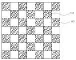
우선, 전극은 터치 전극 영역(112)과 비 터치 전극 영역(113)으로 구분되어 있다. 또한 전극은 메쉬 패턴 형상으로 이루어져 있을 수 있다.First, the electrode is divided into a
예를 들어, 도 3에 도시된 바와 같이 전극 내에서 터치 전극 영역(112)과 비 터치 전극 영역(113)이 바둑판 모양으로 일대일로 나뉘어져 구분되어 있다. 여기서 터치 전극 영역(112)은 단일 전극 내에서 서로 연결되어 있으며, 비 터치 전극 영역(113)은 서로 연결되어 있을 수도 있고, 서로 분리되어 있을 수도 있다. 전극 내의 적어도 하나의 터치 전극 영역(112)에는 콘택홀이 형성되어 있으며, 콘택홀을 통해 배선(130)과 연결되어 있다. 배선과 연결되는 콘택홀은 복수개 형성되어 있을 수도 있다.For example, as shown in FIG. 3, the
그리고, 전극의 모서리는 도 3a에 도시된 바와 같이 형성되어 있을 수 있으며, 도 3b에 도시된 바와 같이 형성되어 있지 않을 수도 있다.The edge of the electrode may be formed as shown in FIG. 3A and may not be formed as shown in FIG. 3B.
이처럼, 전극 내에 비 터치 전극 영역을 형성하여 전극의 초기 정전용량을 저감시킬 수 있으며, 이에 따라 사용자의 터치 입력 전후에 따른 정전용량의 변화량을 증가시켜 터치 감도를 높일 수 있다. 즉, 비 터치 전극 영역을 형성하여 패널 또는 배선들과의 오버랩되는 면적을 감소시키고, 주위에 터치 전극과의 인접하는 부분을 감소시켜 초기 정전용량을 저감시킬 수 있으며 이에 따라 터치 감도를 높일 수 있다.As described above, the non-touch electrode region can be formed in the electrode to reduce the initial capacitance of the electrode. Thus, the touch sensitivity can be increased by increasing the change amount of the capacitance between before and after the touch input by the user. That is, it is possible to reduce the overlapping area with the panel or wires by forming the non-touch electrode region and reduce the adjacent portion with the touch electrode to reduce the initial capacitance, thereby increasing the touch sensitivity .
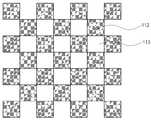
또한, 본 발명의 일 실시예에 따른 전극은 개구부를 포함하여 형성될 수도 있다.In addition, the electrode according to an embodiment of the present invention may include an opening.
예를 들어, 도 4 및 도 5에 도시된 바와 같이, 전극은 사각형 형상 또는 원 형상의 개구부를 포함하여 형성될 수 있으며, 여기서 개구부는 터치 전극 영역(112)이 형성되어 있지 않은 비 터치 전극 영역(113) 부분이다. 전극에서 개구부를 제외한 부분은 터치 전극 영역(112)이다.For example, as shown in FIGS. 4 and 5, the electrode may include a rectangular or circular opening. The opening may be a non-touch electrode region where the
개구부의 형상은 사각형이나 원 형상 뿐만 아니라, 다각형 형상일 수 있으며, 도 4a 및 도 5a에 도시된 바와 같이 개구부끼리 전극 내에서 서로 연결되어 있지 않을 수도 있으나, 도 4b 및 도 5b에 도시된 바와 같이 개구부끼리 전극 내에서 서로 연결되어 있을 수도 있다.4A and 5A, the openings may not be connected to each other in the electrodes. However, as shown in FIGS. 4B and 5B, The openings may be connected to each other within the electrode.
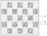
상술한 비 터치 전극 영역(개구부) 내부에는 더미 전극이 형성되어 있을 수도 있다.A dummy electrode may be formed in the non-touch electrode region (opening).
예를 들어 도 6 및 도 7에 도시된 바와 같이, 비 터치 전극 영역(113)에는 사각형 형상 또는 원 형상의 더미 전극(114)이 형성될 수 있다.For example, as shown in FIGS. 6 and 7, a
더미 전극(114)의 형상은 사각형이나 원 형상 뿐만 아니라, 다각형 형상일 수 있으며, 도 6a 및 도 7a에 도시된 바와 같이 더미 전극끼리 전극 내에서 서로 연결되어 있지 않을 수도 있으나, 도 6b 및 도 7b에 도시된 바와 같이 더미 전극끼리 전극 내에서 서로 연결되어 있을 수도 있다.6A and 7A, the
여기서, 더미 전극은 배선이 연결되어 있지 않아 터치 스캔 신호가 인가되지 않거나, 혹은 배선이 연결되어 있더라도 터친 스캔 신호를 전달받지 못하는 물질로 형성되어 있다.Here, the dummy electrode is formed of a material that does not receive a touch scan signal because the wirings are not connected or does not receive a scan signal even if the wirings are connected.
본 발명의 일 실시예에 따른 터치스크린 일체형 표시장치의 다양한 전극 구조의 마지막 실시예로 도 8에 도시된 바와 같이, 전극 내에서 터치 전극 영역(112)과 비 터치 전극 영역(113)이 바둑판 모양으로 일대일로 나뉘어져 구분되어 있는 경우, 비 터치 전극 영역 내에 더미 전극(114)이 형성되어 있을 수도 있다.As shown in FIG. 8, the
여기서, 터치 전극 영역(112)은 서로 연결되어 있고, 더미 전극 영역(114) 또한 서로 연결되어 있다. 그리고, 전극의 모서리는 도 8a에 도시된 바와 같이 형성되어 있을 수 있으며, 도 8b에 도시된 바와 같이 형성되어 있지 않을 수도 있다.
Here, the
다음으로, 도 9는 본 발명의 일 실시예에 따른 터치스크린 일체형 표시장치의 디스플레이 구동과 터치 구동에 대한 신호의 타이밍도이다.Next, FIG. 9 is a timing chart of signals for display driving and touch driving of the touch screen integrated display device according to an embodiment of the present invention.
도 9에 도시된 바와 같이, 한 프레임의 구간에서 패널의 구동모드가 디스플레이 구동모드이면 공통 전압을 m개의 전극으로 인가하여 패널은 디스플레이 구동을 하게 되고, 패널의 구동모드가 터치 구동 모드이면 터치 스캔 신호를 m개의 전극으로 인가하여 패널은 터치 구동을 하게 된다.9, when the driving mode of the panel is a display driving mode in a period of one frame, a common voltage is applied to m electrodes to drive the display, and when the driving mode of the panel is the touch driving mode, The signal is applied to m electrodes, and the panel is touch driven.
예를 들어, 한 프레임 구간을 디스플레이 구동모드 및 터치 구동모드로 분할하여, 디스플레이 구동 기간에는 도 3 내지 도 8에서 언급한 다양한 형태의 전극으로 공통 전압을 인가하고, 터치 구동 기간에는 다양한 형태의 전극으로 터치 스캔 신호를 인가하게 된다.
For example, one frame period is divided into a display driving mode and a touch driving mode. In the display driving period, a common voltage is applied to the electrodes of various types mentioned in FIGS. 3 to 8. In the touch driving period, The touch scan signal is applied.
본 발명이 속하는 기술분야의 당업자는 상술한 본 발명이 그 기술적 사상이나 필수적 특징을 변경하지 않고서 다른 구체적인 형태로 실시될 수 있다는 것을 이해할 수 있을 것이다.It will be understood by those skilled in the art that the present invention may be embodied in other specific forms without departing from the spirit or essential characteristics thereof.
그러므로, 이상에서 기술한 실시예는 모든 면에서 예시적인 것이며 한정적인 것이 아닌 것으로 이해해야만 한다. 본 발명의 범위는 상기 상세한 설명보다는 후술하는 특허청구범위에 의하여 나타내어지며, 특허청구범위의 의미 및 범위 그리고 그 등가 개념으로부터 도출되는 모든 변경 또는 변형된 형태가 본 발명의 범위에 포함되는 것으로 해석되어야 한다.
Therefore, it should be understood that the above-described embodiments are illustrative in all aspects and not restrictive. The scope of the present invention is defined by the appended claims rather than the detailed description and all changes or modifications derived from the meaning and scope of the claims and their equivalents are to be construed as being included within the scope of the present invention do.
100 : 패널 110 : 표시 영역
111 : 전극 112 : 터치 전극 영역
113 : 비 터치 전극 영역 114 : 더미 전극부
120 : 비 표시 영역 200 : 디스플레이 드라이버 IC
210 : 공통전압 생성부 220 : 동기신호 생성부
230 : 스위칭부 300 : 터치 IC
310 : 스캔 신호 생성부 320 : 터치 감지부100: Panel 110: Display area
111: electrode 112: touch electrode region
113: non-touch electrode region 114: dummy electrode portion
120: Non-display area 200: Display driver IC
210: common voltage generator 220: synchronous signal generator
230: Switching part 300: Touch IC
310: scan signal generator 320:
Claims (14)
Translated fromKorean상기 m개의 전극으로 공통 전압을 인가하는 디스플레이 드라이버 IC;
터치 스캔 신호를 생성하여 상기 m개의 전극으로 인가하고 상기 터치 스캔 신호에 따른 터치 감지 신호를 상기 m개의 전극으로부터 수신하여 상기 패널 내의 터치 입력 위치를 감지하는 터치 IC;
상기 m개의 전극 중 적어도 하나의 전극은 터치 전극 영역과 비 터치 전극 영역으로 구분되어 있고,
상기 비 터치 전극 영역은 상기 터치 스캔 신호가 인가되는 터치 전극 영역이 형성되어 있지 않은 개구부이고,
상기 개구부들은 서로 연결되어 있는
터치스크린 일체형 표시장치.
a panel comprising m electrodes and m wires;
A display driver IC for applying a common voltage to the m electrodes;
A touch IC for generating a touch scan signal to be applied to the m electrodes and receiving a touch detection signal corresponding to the touch scan signal from the m electrodes to sense a touch input position in the panel;
At least one of the m electrodes is divided into a touch electrode region and a non-touch electrode region,
Wherein the non-touch electrode region is an opening in which the touch electrode region to which the touch scan signal is applied is not formed,
The openings are connected to each other
A touch screen integrated display device.
상기 패널은 표시 영역과 비표시 영역으로 구분되어 있으며, 상기 m개의 전극은 상기 표시 영역에 형성되고, 상기 디스플레이 드라이버 IC는 상기 비표시 영역에 형성되는 것을 특징으로 하는 터치스크린 일체형 표시장치.
The method according to claim 1,
Wherein the panel is divided into a display area and a non-display area, the m electrodes are formed in the display area, and the display driver IC is formed in the non-display area.
상기 터치 IC는 상기 비표시 영역에 형성되거나 상기 디스플레이 드라이버 IC 내부에 형성되는 것을 특징으로 하는 터치스크린 일체형 표시장치.3. The method of claim 2,
Wherein the touch IC is formed in the non-display area or inside the display driver IC.
상기 디스플레이 드라이버 IC는 상기 패널의 구동모드가 디스플레이 구동모드이면 상기 m개의 전극으로 상기 공통 전압을 인가하고, 상기 터치 IC는 패널의 구동모드가 터치 구동모드이면 상기 m개의 전극으로 상기 터치 스캔 신호를 인가하는 것을 특징으로 하는 터치스크린 일체형 표시장치.
The method according to claim 1,
Wherein the display driver IC applies the common voltage to the m electrodes when the driving mode of the panel is a display driving mode and the touch IC uses the m electrodes to turn on the touch scan signal when the driving mode of the panel is the touch driving mode Wherein the touch screen type display device is a touch screen type display device.
상기 디스플레이 드라이버 IC는,
상기 공통 전압을 생성하는 공통 전압 생성부;
상기 디스플레이 구동모드 및 상기 터치 구동모드를 지시하는 동기신호를 생성하는 동기신호 생성부;
상기 동기신호에 따라 상기 공통 전압 생성부와 상기 m개의 전극이 연결되도록 하거나, 상기 터치 IC와 상기 m개의 전극이 연결되도록 하는 스위칭부를 포함하는 것을 특징으로 하는 터치스크린 일체형 표시장치.
5. The method of claim 4,
The display driver IC includes:
A common voltage generator for generating the common voltage;
A synchronization signal generating unit for generating a synchronization signal indicating the display driving mode and the touch driving mode;
And a switching unit for connecting the common voltage generator and the m electrodes according to the synchronization signal or for connecting the touch IC to the m electrodes.
상기 터치 IC는,
상기 터치 스캔 신호를 생성하는 터치 스캔 신호 생성부; 및
상기 m개의 전극으로부터 상기 터치 스캔 신호에 따른 터치 감지 신호를 수신하여 상기 패널 내의 터치 입력 위치를 감지하는 터치 감지부를 포함하는 것을 특징으로 하는 터치스크린 일체형 표시장치.
The method according to claim 1,
The touch IC includes:
A touch scan signal generator for generating the touch scan signal; And
And a touch sensing unit for sensing a touch input position in the panel by receiving a touch sensing signal corresponding to the touch scan signal from the m electrodes.
상기 터치 IC는 상기 디스플레이 드라이버 IC를 통해 상기 터치 스캔 신호를 인가하고 상기 터치 감지 신호를 수신하는 것을 특징으로 하는 터치스크린 일체형 표시장치.
The method according to claim 6,
Wherein the touch IC applies the touch scan signal through the display driver IC and receives the touch sensing signal.
상기 개구부의 형상은 사각형을 포함하는 다각형 형상이거나 원형 형상인 것을 특징으로 하는 터치스크린 일체형 표시장치.
The method according to claim 1,
Wherein the shape of the opening is a polygonal shape including a quadrangle or a circular shape.
상기 비 터치 전극 영역 내에는 터치 스캔 신호가 인가되지 않는 더미 전극이 형성되어 있는 것을 특징으로 하는 터치스크린 일체형 표시장치.
The method according to claim 1,
Wherein the non-touch electrode region is formed with a dummy electrode to which no touch scan signal is applied.
상기 더미 전극의 형상은 사각형을 포함하는 다각형 형상이거나 원 형상인 것을 특징으로 하는 터치스크린 일체형 표시장치.
12. The method of claim 11,
Wherein the shape of the dummy electrode is a polygonal shape including a quadrangle or a circular shape.
상기 더미 전극들은 서로 연결되어 있는 것을 특징으로 하는 터치스크린 일체형 표시장치.
12. The method of claim 11,
And the dummy electrodes are connected to each other.
상기 m개의 전극 중 적어도 하나의 전극은 메쉬(mesh) 패턴인 것을 특징으로 하는 터치스크린 일체형 표시장치.
The method according to claim 1,
Wherein at least one of the m electrodes is a mesh pattern.
Priority Applications (3)
| Application Number | Priority Date | Filing Date | Title |
|---|---|---|---|
| KR1020130135610AKR101736937B1 (en) | 2013-11-08 | 2013-11-08 | Display device with integrated touch screen |
| US14/478,592US10031626B2 (en) | 2013-11-08 | 2014-09-05 | Display device with integrated touch screen |
| CN201410503185.8ACN104636012B (en) | 2013-11-08 | 2014-09-26 | Display device with integrated touch-screen |
Applications Claiming Priority (1)
| Application Number | Priority Date | Filing Date | Title |
|---|---|---|---|
| KR1020130135610AKR101736937B1 (en) | 2013-11-08 | 2013-11-08 | Display device with integrated touch screen |
Publications (2)
| Publication Number | Publication Date |
|---|---|
| KR20150053537A KR20150053537A (en) | 2015-05-18 |
| KR101736937B1true KR101736937B1 (en) | 2017-05-17 |
Family
ID=53043393
Family Applications (1)
| Application Number | Title | Priority Date | Filing Date |
|---|---|---|---|
| KR1020130135610AActiveKR101736937B1 (en) | 2013-11-08 | 2013-11-08 | Display device with integrated touch screen |
Country Status (3)
| Country | Link |
|---|---|
| US (1) | US10031626B2 (en) |
| KR (1) | KR101736937B1 (en) |
| CN (1) | CN104636012B (en) |
Families Citing this family (27)
| Publication number | Priority date | Publication date | Assignee | Title |
|---|---|---|---|---|
| CN103926729B (en)* | 2013-12-31 | 2017-12-22 | 上海天马微电子有限公司 | Array substrate, color film substrate, touch display device and driving method thereof |
| US10209834B2 (en)* | 2014-10-01 | 2019-02-19 | Microsoft Technology Licensing, Llc | Integrated self-capacitive touch display |
| KR20160086528A (en)* | 2015-01-09 | 2016-07-20 | 삼성디스플레이 주식회사 | Touch panel and display device comprising the same |
| US9939972B2 (en)* | 2015-04-06 | 2018-04-10 | Synaptics Incorporated | Matrix sensor with via routing |
| CN104808858B (en)* | 2015-05-08 | 2018-07-10 | 厦门天马微电子有限公司 | A kind of touch panel and touch control display apparatus |
| CN106249454B (en)* | 2015-06-12 | 2019-10-25 | 群创光电股份有限公司 | touch monitor |
| US9671915B2 (en) | 2015-06-30 | 2017-06-06 | Synaptics Incorporated | Avoidance of bending effects in a touch sensor device |
| CN106406591B (en)* | 2015-07-31 | 2019-11-26 | 昆山国显光电有限公司 | OLED touch base plate, its manufacturing method and control method |
| CN104965629A (en)* | 2015-08-07 | 2015-10-07 | 信利光电股份有限公司 | Touch screen and electronic device |
| CN104991690B (en)* | 2015-08-11 | 2018-05-18 | 京东方科技集团股份有限公司 | A kind of touch-control display panel, its production method, driving method and display device |
| KR101747263B1 (en) | 2015-09-25 | 2017-06-14 | 엘지디스플레이 주식회사 | Driver integrated circuit and display apparatus using the same |
| US9971463B2 (en) | 2015-09-29 | 2018-05-15 | Synaptics Incorporated | Row-based sensing on matrix pad sensors |
| CN105677126B (en) | 2016-02-04 | 2020-03-27 | 上海天马微电子有限公司 | Display panel and display device |
| US10474289B2 (en)* | 2016-04-07 | 2019-11-12 | GM Global Technology Operations LLC | Touchscreen panel with heating function |
| KR102054734B1 (en)* | 2016-07-19 | 2019-12-11 | 보에 테크놀로지 그룹 컴퍼니 리미티드 | Touch substrate, mask plate for manufacturing same, and manufacturing method thereof |
| CN106803085A (en)* | 2016-11-30 | 2017-06-06 | 努比亚技术有限公司 | A kind of terminal and scanning implementation method |
| CN107026191B (en)* | 2017-05-03 | 2020-05-26 | 京东方科技集团股份有限公司 | OLED display device and control method thereof |
| KR102349699B1 (en)* | 2017-05-31 | 2022-01-10 | 엘지디스플레이 주식회사 | Display device with integrated touch screen and method for fabricating the same |
| US10379688B2 (en) | 2017-06-14 | 2019-08-13 | Synaptics Incorporated | Transcapacitive matrix sensor with via routing |
| CN107229153B (en)* | 2017-07-07 | 2019-11-22 | 昆山龙腾光电有限公司 | Embedded touch control type array substrate and production method and display device |
| KR102352750B1 (en)* | 2017-09-11 | 2022-01-17 | 엘지디스플레이 주식회사 | Touch Display Device |
| KR102079389B1 (en)* | 2017-09-29 | 2020-02-19 | 주식회사 센트론 | Display using passive matrix organic light emitting diode |
| KR102456333B1 (en)* | 2017-10-23 | 2022-10-19 | 엘지디스플레이 주식회사 | Touch display device and panel |
| KR102411682B1 (en)* | 2017-11-16 | 2022-06-21 | 엘지디스플레이 주식회사 | Touch display device and panel |
| US10942608B2 (en) | 2018-04-24 | 2021-03-09 | Synaptics Incorporated | Spatially encoded sensor electrodes |
| US20200103991A1 (en)* | 2018-09-29 | 2020-04-02 | Wuhan China Star Optoelectronics Technology Co., Ltd. | Display panel, display module and electronic device |
| CN114170938B (en)* | 2021-11-24 | 2023-11-21 | 云谷(固安)科技有限公司 | Display panel and display device |
Citations (1)
| Publication number | Priority date | Publication date | Assignee | Title |
|---|---|---|---|---|
| US20120169655A1 (en) | 2010-12-30 | 2012-07-05 | Egalax_Empia Technology Inc. | Capacitive touch screen |
Family Cites Families (19)
| Publication number | Priority date | Publication date | Assignee | Title |
|---|---|---|---|---|
| KR20100006987A (en)* | 2008-07-11 | 2010-01-22 | 삼성모바일디스플레이주식회사 | Touch screen panel and fabricating method for the same |
| JP5033078B2 (en)* | 2008-08-06 | 2012-09-26 | 株式会社ジャパンディスプレイイースト | Display device |
| CN101943975B (en) | 2009-07-09 | 2015-12-16 | 敦泰科技有限公司 | Ultra-thin mutual capacitance touch screen and combined ultra-thin touch screen |
| TWI494828B (en) | 2009-07-29 | 2015-08-01 | Cando Corp | Capacitive touch panel with reduced visibility for sensor structure |
| JP5458443B2 (en)* | 2010-09-14 | 2014-04-02 | 株式会社ジャパンディスプレイ | Display device with touch detection function and electronic device |
| CN202003341U (en) | 2011-03-15 | 2011-10-05 | 德理投资股份有限公司 | Projected Capacitive Touch Panel with Sensitivity Adjustment Structure |
| KR101706242B1 (en) | 2011-04-27 | 2017-02-14 | 엘지디스플레이 주식회사 | In-cell Type Touch Panel |
| KR101853025B1 (en) | 2011-07-27 | 2018-04-27 | 엘지디스플레이 주식회사 | Touch screen panel |
| US8994673B2 (en)* | 2011-12-09 | 2015-03-31 | Lg Display Co., Ltd. | Display device with integrated touch screen having electrical connections provided in inactive regions of display panel |
| KR101524449B1 (en) | 2011-12-22 | 2015-06-02 | 엘지디스플레이 주식회사 | Liquid crystal display device and Method for manufacturing the same |
| KR101330320B1 (en)* | 2012-02-20 | 2013-11-14 | 엘지디스플레이 주식회사 | Display device with integrated touch screen and method for driving the same |
| TWI436411B (en) | 2012-04-27 | 2014-05-01 | Liu Hung Ta | Touch device |
| KR101416003B1 (en)* | 2012-06-20 | 2014-07-08 | 엘지디스플레이 주식회사 | Display device with integrated touch screen and method for driving the same |
| KR101480314B1 (en)* | 2012-08-16 | 2015-01-08 | 엘지디스플레이 주식회사 | Display device with integrated touch screen and method for driving the same |
| KR101628724B1 (en)* | 2012-11-13 | 2016-06-09 | 엘지디스플레이 주식회사 | Display device with integrated touch screen |
| CN202948433U (en) | 2012-12-14 | 2013-05-22 | 北京京东方光电科技有限公司 | Capacitor type embedded touch screen and display device |
| TWI521288B (en)* | 2013-03-07 | 2016-02-11 | 友達光電股份有限公司 | An array of touch unit and a display panel having the same |
| CN203178998U (en) | 2013-04-07 | 2013-09-04 | 北京京东方光电科技有限公司 | Capacitive in cell touch panel and display device |
| US9372573B2 (en)* | 2013-05-31 | 2016-06-21 | Boe Technology Group Co., Ltd. | Array substrate, touch panel and driving method thereof |
- 2013
- 2013-11-08KRKR1020130135610Apatent/KR101736937B1/enactiveActive
- 2014
- 2014-09-05USUS14/478,592patent/US10031626B2/enactiveActive
- 2014-09-26CNCN201410503185.8Apatent/CN104636012B/enactiveActive
Patent Citations (1)
| Publication number | Priority date | Publication date | Assignee | Title |
|---|---|---|---|---|
| US20120169655A1 (en) | 2010-12-30 | 2012-07-05 | Egalax_Empia Technology Inc. | Capacitive touch screen |
Also Published As
| Publication number | Publication date |
|---|---|
| CN104636012B (en) | 2018-02-06 |
| US20150130753A1 (en) | 2015-05-14 |
| KR20150053537A (en) | 2015-05-18 |
| US10031626B2 (en) | 2018-07-24 |
| CN104636012A (en) | 2015-05-20 |
Similar Documents
| Publication | Publication Date | Title |
|---|---|---|
| KR101736937B1 (en) | Display device with integrated touch screen | |
| KR101641690B1 (en) | Display device with integrated touch screen | |
| JP5665957B2 (en) | Touch screen integrated display | |
| KR101570455B1 (en) | Display device with integrated touch screen and method for driving the same | |
| KR101606874B1 (en) | Display device with integrated touch screen and method for driving the same | |
| EP2869166B1 (en) | Touch panel, touch display panel, and touch detection and display method | |
| JP2018206351A (en) | Touch display device and method for driving touch display device | |
| KR101360782B1 (en) | Display device with integrated touch screen | |
| KR102133736B1 (en) | Display device with integrated touch screen and method for driving the same | |
| KR20160019625A (en) | Touch sensor integrated type display device | |
| KR101733728B1 (en) | Display device with integrated touch screen | |
| KR20190029045A (en) | Touch Display Device | |
| KR101723879B1 (en) | Display device with integrated touch screen | |
| KR101720997B1 (en) | Display device with integrated touch screen | |
| KR102198495B1 (en) | Display device with integrated touch screen | |
| KR101795998B1 (en) | Display device with integrated touch screen and method for driving the same | |
| KR101818548B1 (en) | Display device with integrated touch screen and touch integrated circuit | |
| KR101688428B1 (en) | Display driver ic, display device with integrated touch screen and method for driving the same | |
| KR20140082201A (en) | Display device with integrated touch screen and method for driving the same |
Legal Events
| Date | Code | Title | Description |
|---|---|---|---|
| PA0109 | Patent application | Patent event code:PA01091R01D Comment text:Patent Application Patent event date:20131108 | |
| A201 | Request for examination | ||
| PA0201 | Request for examination | Patent event code:PA02012R01D Patent event date:20150312 Comment text:Request for Examination of Application Patent event code:PA02011R01I Patent event date:20131108 Comment text:Patent Application | |
| PG1501 | Laying open of application | ||
| E902 | Notification of reason for refusal | ||
| PE0902 | Notice of grounds for rejection | Comment text:Notification of reason for refusal Patent event date:20160630 Patent event code:PE09021S01D | |
| E701 | Decision to grant or registration of patent right | ||
| PE0701 | Decision of registration | Patent event code:PE07011S01D Comment text:Decision to Grant Registration Patent event date:20170302 | |
| GRNT | Written decision to grant | ||
| PR0701 | Registration of establishment | Comment text:Registration of Establishment Patent event date:20170511 Patent event code:PR07011E01D | |
| PR1002 | Payment of registration fee | Payment date:20170511 End annual number:3 Start annual number:1 | |
| PG1601 | Publication of registration | ||
| PR1001 | Payment of annual fee | Payment date:20200422 Start annual number:4 End annual number:4 | |
| PR1001 | Payment of annual fee | Payment date:20210415 Start annual number:5 End annual number:5 | |
| PR1001 | Payment of annual fee | Payment date:20230417 Start annual number:7 End annual number:7 | |
| PR1001 | Payment of annual fee | Payment date:20240415 Start annual number:8 End annual number:8 | |
| PR1001 | Payment of annual fee | Payment date:20250415 Start annual number:9 End annual number:9 |