KR101736319B1 - Organic light emitting display device and manufacturing method of the same - Google Patents
Organic light emitting display device and manufacturing method of the sameDownload PDFInfo
- Publication number
- KR101736319B1 KR101736319B1KR1020100127856AKR20100127856AKR101736319B1KR 101736319 B1KR101736319 B1KR 101736319B1KR 1020100127856 AKR1020100127856 AKR 1020100127856AKR 20100127856 AKR20100127856 AKR 20100127856AKR 101736319 B1KR101736319 B1KR 101736319B1
- Authority
- KR
- South Korea
- Prior art keywords
- electrode
- capacitor
- layer
- light emitting
- metal
- Prior art date
- Legal status (The legal status is an assumption and is not a legal conclusion. Google has not performed a legal analysis and makes no representation as to the accuracy of the status listed.)
- Active
Links
Images


Classifications
- H—ELECTRICITY
- H10—SEMICONDUCTOR DEVICES; ELECTRIC SOLID-STATE DEVICES NOT OTHERWISE PROVIDED FOR
- H10K—ORGANIC ELECTRIC SOLID-STATE DEVICES
- H10K59/00—Integrated devices, or assemblies of multiple devices, comprising at least one organic light-emitting element covered by group H10K50/00
- H10K59/10—OLED displays
- H10K59/12—Active-matrix OLED [AMOLED] displays
- H10K59/121—Active-matrix OLED [AMOLED] displays characterised by the geometry or disposition of pixel elements
- H—ELECTRICITY
- H10—SEMICONDUCTOR DEVICES; ELECTRIC SOLID-STATE DEVICES NOT OTHERWISE PROVIDED FOR
- H10D—INORGANIC ELECTRIC SEMICONDUCTOR DEVICES
- H10D30/00—Field-effect transistors [FET]
- H10D30/60—Insulated-gate field-effect transistors [IGFET]
- H10D30/67—Thin-film transistors [TFT]
- H10D30/6729—Thin-film transistors [TFT] characterised by the electrodes
- H10D30/673—Thin-film transistors [TFT] characterised by the electrodes characterised by the shapes, relative sizes or dispositions of the gate electrodes
- H10D30/6733—Multi-gate TFTs
- H—ELECTRICITY
- H10—SEMICONDUCTOR DEVICES; ELECTRIC SOLID-STATE DEVICES NOT OTHERWISE PROVIDED FOR
- H10D—INORGANIC ELECTRIC SEMICONDUCTOR DEVICES
- H10D30/00—Field-effect transistors [FET]
- H10D30/60—Insulated-gate field-effect transistors [IGFET]
- H10D30/67—Thin-film transistors [TFT]
- H10D30/6729—Thin-film transistors [TFT] characterised by the electrodes
- H10D30/6737—Thin-film transistors [TFT] characterised by the electrodes characterised by the electrode materials
- H10D30/6739—Conductor-insulator-semiconductor electrodes
- H—ELECTRICITY
- H10—SEMICONDUCTOR DEVICES; ELECTRIC SOLID-STATE DEVICES NOT OTHERWISE PROVIDED FOR
- H10D—INORGANIC ELECTRIC SEMICONDUCTOR DEVICES
- H10D30/00—Field-effect transistors [FET]
- H10D30/60—Insulated-gate field-effect transistors [IGFET]
- H10D30/67—Thin-film transistors [TFT]
- H10D30/6757—Thin-film transistors [TFT] characterised by the structure of the channel, e.g. transverse or longitudinal shape or doping profile
- H—ELECTRICITY
- H10—SEMICONDUCTOR DEVICES; ELECTRIC SOLID-STATE DEVICES NOT OTHERWISE PROVIDED FOR
- H10D—INORGANIC ELECTRIC SEMICONDUCTOR DEVICES
- H10D86/00—Integrated devices formed in or on insulating or conducting substrates, e.g. formed in silicon-on-insulator [SOI] substrates or on stainless steel or glass substrates
- H10D86/40—Integrated devices formed in or on insulating or conducting substrates, e.g. formed in silicon-on-insulator [SOI] substrates or on stainless steel or glass substrates characterised by multiple TFTs
- H10D86/481—Integrated devices formed in or on insulating or conducting substrates, e.g. formed in silicon-on-insulator [SOI] substrates or on stainless steel or glass substrates characterised by multiple TFTs integrated with passive devices, e.g. auxiliary capacitors
- H—ELECTRICITY
- H10—SEMICONDUCTOR DEVICES; ELECTRIC SOLID-STATE DEVICES NOT OTHERWISE PROVIDED FOR
- H10D—INORGANIC ELECTRIC SEMICONDUCTOR DEVICES
- H10D86/00—Integrated devices formed in or on insulating or conducting substrates, e.g. formed in silicon-on-insulator [SOI] substrates or on stainless steel or glass substrates
- H10D86/40—Integrated devices formed in or on insulating or conducting substrates, e.g. formed in silicon-on-insulator [SOI] substrates or on stainless steel or glass substrates characterised by multiple TFTs
- H10D86/60—Integrated devices formed in or on insulating or conducting substrates, e.g. formed in silicon-on-insulator [SOI] substrates or on stainless steel or glass substrates characterised by multiple TFTs wherein the TFTs are in active matrices
- H—ELECTRICITY
- H10—SEMICONDUCTOR DEVICES; ELECTRIC SOLID-STATE DEVICES NOT OTHERWISE PROVIDED FOR
- H10K—ORGANIC ELECTRIC SOLID-STATE DEVICES
- H10K59/00—Integrated devices, or assemblies of multiple devices, comprising at least one organic light-emitting element covered by group H10K50/00
- H10K59/10—OLED displays
- H10K59/12—Active-matrix OLED [AMOLED] displays
- H10K59/1201—Manufacture or treatment
- H—ELECTRICITY
- H10—SEMICONDUCTOR DEVICES; ELECTRIC SOLID-STATE DEVICES NOT OTHERWISE PROVIDED FOR
- H10K—ORGANIC ELECTRIC SOLID-STATE DEVICES
- H10K59/00—Integrated devices, or assemblies of multiple devices, comprising at least one organic light-emitting element covered by group H10K50/00
- H10K59/10—OLED displays
- H10K59/12—Active-matrix OLED [AMOLED] displays
- H10K59/121—Active-matrix OLED [AMOLED] displays characterised by the geometry or disposition of pixel elements
- H10K59/1216—Active-matrix OLED [AMOLED] displays characterised by the geometry or disposition of pixel elements the pixel elements being capacitors
Landscapes
- Engineering & Computer Science (AREA)
- Microelectronics & Electronic Packaging (AREA)
- Physics & Mathematics (AREA)
- Geometry (AREA)
- Manufacturing & Machinery (AREA)
- Electroluminescent Light Sources (AREA)
- Devices For Indicating Variable Information By Combining Individual Elements (AREA)
Abstract
Translated fromKoreanDescription
Translated fromKorean본 발명은 유기 발광 표시 장치 및 그 제조 방법에 관한 것이다.The present invention relates to an organic light emitting display and a method of manufacturing the same.
유기 발광 표시 장치는 경량 박형이 가능할 뿐만 아니라, 넓은 시야각, 빠른 응답속도 및 적은 소비 전력 등의 장점으로 인하여 차세대 표시 장치로서 주목 받고 있다.The organic light emitting display device has been attracting attention as a next generation display device because of its advantages such as light weight and thinness, wide viewing angle, fast response speed and low power consumption.
본 발명은 제조 공정이 단순하고, 개구율이 우수한 유기 발광 표시 장치 및 그 제조 방법을 제공하는 것을 목적으로 한다.It is an object of the present invention to provide an organic light emitting display device having a simple manufacturing process and excellent aperture ratio and a method of manufacturing the same.
본 발명의 일 측면에 의하면, 반도체층, 게이트 전극, 및 소스 및 드레인 전극이 구비된 적어도 하나 이상의 트랜지스터; 상기 반도체층과 동일층에 형성된 제1전극, 상기 게이트 전극과 동일층에 형성된 제2전극, 및 상기 소스 및 드레인 전극과 동일층에 형성된 제3전극이 구비된 제1커패시터; 상기 반도체층과 동일층에 형성되고 도핑된 이온 불순물을 포함하는 제1전극, 및 상기 게이트 전극과 동일층에 형성된 제2전극이 구비된 제2커패시터; 상기 게이트 전극과 동일층에 형성되고, 상기 트랜지스터에 전기적으로 연결된 화소 전극; 상기 화소 전극 상에 위치하는 발광층; 및 상기 발광층을 사이에 두고 상기 화소 전극에 대향 배치되는 대향 전극;을 포함하는 유기 발광 표시 장치를 제공한다. According to an aspect of the present invention, there is provided a semiconductor device comprising: at least one transistor including a semiconductor layer, a gate electrode, and source and drain electrodes; A first capacitor having a first electrode formed on the same layer as the semiconductor layer, a second electrode formed on the same layer as the gate electrode, and a third electrode formed on the same layer as the source and drain electrodes; A second capacitor formed on the same layer as the semiconductor layer and including a first electrode including a doped ion impurity and a second electrode formed on the same layer as the gate electrode; A pixel electrode formed on the same layer as the gate electrode and electrically connected to the transistor; A light emitting layer disposed on the pixel electrode; And a counter electrode disposed opposite to the pixel electrode with the light emitting layer interposed therebetween.
본 발명의 다른 특징에 의하면, 상기 제1커패시터는 상기 적어도 하나의 트랜지스터에 전원 전압을 공급하는 전원 전압 공급선과 연결되고, 상기 전원 전압 공급선과 중첩되도록 위치할 수 있다.According to another aspect of the present invention, the first capacitor may be connected to a power supply voltage supply line for supplying a power supply voltage to the at least one transistor, and may be positioned to overlap with the power supply voltage supply line.
본 발명의 또 다른 특징에 의하면, 상기 적어도 하나의 트랜지스터는 구동 트랜지스터이고, 상기 제1커패시터는 상기 구동 트랜지스터에 전압을 인가하는 저장 커패시터일 수 있다.According to another aspect of the present invention, the at least one transistor is a driving transistor, and the first capacitor may be a storage capacitor for applying a voltage to the driving transistor.
본 발명의 또 다른 특징에 의하면, 상기 제1커패시터의 제1전극은 이온 불순물이 도핑되지 않은 반도체를 포함할 수 있다.According to another aspect of the present invention, the first electrode of the first capacitor may include a semiconductor that is not doped with ionic impurities.
본 발명의 또 다른 특징에 의하면, 상기 제1커패시터의 제1전극과 제3전극은 접속홀을 통하여 연결될 수 있다.According to another aspect of the present invention, the first electrode and the third electrode of the first capacitor may be connected through a connection hole.
본 발명의 또 다른 특징에 의하면, 상기 제1커패시터는 상기 제1전극과 상기 제2전극 사이에 형성된 제1정전용량, 및 상기 제2전극과 상기 제3전극 사이에 형성된 제2정전용량이 병렬 연결될 수 있다.According to still another aspect of the present invention, the first capacitor includes a first capacitance formed between the first electrode and the second electrode, and a second capacitance formed between the second electrode and the third electrode, Can be connected.
본 발명의 또 다른 특징에 의하면, 상기 제1커패시터의 제2전극은 상기 게이트 전극과 동일한 물질을 포함할 수 있다.According to another aspect of the present invention, the second electrode of the first capacitor may include the same material as the gate electrode.
본 발명의 또 다른 특징에 의하면, 상기 제1커패시터의 제3전극은 상기 소스 및 드레인 전극과 동일한 물질을 포함할 수 있다.According to another aspect of the present invention, the third electrode of the first capacitor may include the same material as the source and drain electrodes.
본 발명의 또 다른 특징에 의하면, 상기 제1커패시터의 제3전극은 상기 적어도 하나의 트랜지스터에 전원 전압을 공급하는 전원 전압 공급선을 포함할 수 있다.According to another aspect of the present invention, the third electrode of the first capacitor may include a power supply voltage supply line for supplying a power supply voltage to the at least one transistor.
본 발명의 또 다른 특징에 의하면, 상기 제2커패시터는 구동 트랜지스터의 게이트 단자에 연결된 보상 커패시터일 수 있다.According to another aspect of the present invention, the second capacitor may be a compensation capacitor connected to the gate terminal of the driving transistor.
본 발명의 또 다른 특징에 의하면, 상기 제2커패시터의 제2전극은 투명도전물일 수 있다.According to another aspect of the present invention, the second electrode of the second capacitor may be a transparent conductive material.
본 발명의 또 다른 특징에 의하면, 상기 게이트 전극은 투명도전물을 포함하는 제1층, 및 금속을 포함하는 제2층을 구비할 수 있다. According to another aspect of the present invention, the gate electrode may include a first layer including a transparent conductive material, and a second layer including a metal.
본 발명의 또 다른 특징에 의하면, 상기 화소 전극은 상기 게이트 전극의 투명도전물로 구비될 수 있다.According to another aspect of the present invention, the pixel electrode may be formed of a transparent conductive material of the gate electrode.
본 발명의 또 다른 특징에 의하면, 상기 반도체층은 비정질 실리콘 또는 결정질 실리콘일 수 있다.According to another aspect of the present invention, the semiconductor layer may be amorphous silicon or crystalline silicon.
본 발명의 또 다른 특징에 의하면, 상기 대향 전극은 상기 발광층에서 방출된 광을 반사하는 반사 전극일 수 있다.According to another aspect of the present invention, the counter electrode may be a reflective electrode that reflects light emitted from the light emitting layer.
본 발명의 다른 측면에 의하면, 기판 상에 반도체층을 형성하고, 상기 반도체층을 패터닝하여 트랜지스터의 반도체층, 제1 및 제2커패시터의 제1전극을 형성하는 제1마스크 공정; 제1마스크 공정의 결과물 상에 제1절연층을 형성하고, 상기 제1절연층 상에 투명도전물 및 제1금속을 차례로 형성하고 이를 패터닝하여, 트랜지스터의 게이트 전극, 화소 전극, 제1 및 제2커패시터의 제2전극을 형성하는 제2마스크 공정; 제2마스크 공정의 결과물 상에 제2절연층을 형성하고, 상기 반도체층의 소스 및 드레인 영역, 상기 화소 전극, 상기 제1커패시터의 제1전극 일부, 및 상기 제2커패시터의 제2전극을 노출시키는 콘택홀들을 형성하는 제3마스크 공정; 제3마스크 공정의 결과물 상에 제2금속을 형성하고, 상기 제2금속을 패터닝하여 상기 소스 및 드레인 영역과 접속하는 소스 및 드레인 전극, 및 상기 제1커패시터의 제3전극을 형성하는 제4마스크 공정; 및 제4마스크 공정의 결과물 상에 제3절연층을 형성하고, 상기 화소 전극의 투명도전물이 노출되도록 제3절연층을 개구시키는 제5마스크 공정;을 포함하는 유기 발광 표시 장치의 제조 방법을 제공한다.According to another aspect of the present invention, there is provided a method of manufacturing a semiconductor device, comprising: forming a semiconductor layer on a substrate, patterning the semiconductor layer to form a semiconductor layer of the transistor, a first electrode of the first and second capacitors; Forming a first insulating layer on the result of the first mask process, sequentially forming a transparent conductive material and a first metal on the first insulating layer, and patterning the same to form a gate electrode, a pixel electrode, A second mask process for forming a second electrode of the second capacitor; Forming a second insulating layer on the result of the second mask process, exposing the source and drain regions of the semiconductor layer, the pixel electrode, a first electrode portion of the first capacitor, and a second electrode of the second capacitor, A third masking step of forming contact holes to expose the contact holes; Forming a second metal on the resultant of the third masking process, patterning the second metal to form source and drain electrodes connected to the source and drain regions, and forming a third electrode of the first capacitor, fair; And a fifth masking step of forming a third insulating layer on the result of the fourth masking step and opening the third insulating layer so that the transparent conductive material of the pixel electrode is exposed. to provide.
본 발명의 다른 특징에 의하면, 상기 제2마스크 공정 후, 상기 소스 및 드레인 영역에 이온 불순물을 도핑할 수 있다.According to another aspect of the present invention, after the second mask process, the source and drain regions may be doped with ionic impurities.
본 발명의 또 다른 특징에 의하면, 상기 제4마스크 공정은, 상기 화소 전극 및 제2커패시터의 제2전극 상에 적층된 상기 제2금속을 제거하는 제1식각 공정, 상기 화소 전극 및 제2커패시터의 투명도전물 상에 형성된 상기 제1금속을 제거하는 제2식각 공정을 포함할 수 있다.According to another aspect of the present invention, the fourth mask process includes a first etching process for removing the second metal stacked on the second electrode of the pixel electrode and the second capacitor, a second etching process for removing the second metal stacked on the second electrode of the pixel electrode and the second capacitor, And a second etching process for removing the first metal formed on the transparent conductive layer.
본 발명의 또 다른 특징에 의하면, 상기 제4마스크 공정에서, 상기 제2금속은 상기 제1금속과 동일 재료로 형성되고, 상기 제1금속 및 제2금속을 동시에 식각할 수 있다.According to still another aspect of the present invention, in the fourth mask process, the second metal is formed of the same material as the first metal, and the first metal and the second metal are simultaneously etched.
본 발명의 또 다른 특징에 의하면, 상기 제4마스크 공정 후, 상기 제2커패시터의 제1전극에 이온 불순물을 도핑할 수 있다.According to another aspect of the present invention, after the fourth mask process, the first electrode of the second capacitor may be doped with an ionic impurity.
본 발명의 또 다른 특징에 의하면, 상기 제5마스크 공정 후, 상기 화소 전극 상부에 발광층, 및 대향 전극을 더 형성할 수 있다.According to still another aspect of the present invention, after the fifth mask process, a light emitting layer and an opposite electrode may be further formed on the pixel electrode.
상기와 같은 본 발명에 따른 유기 발광 표시 장치 및 그 제조 방법에 따르면 다음과 같은 효과를 제공한다.The organic light emitting diode display according to the present invention and the method of manufacturing the same provide the following advantages.
첫째, 저장 커패시터를 전원전압공급 라인에 중첩하여 형성함으로써, 발광 영역의 면적 증가에 따른 개구율을 향상시킬 수 있다.First, by forming the storage capacitor over the power supply voltage supply line, it is possible to improve the aperture ratio as the area of the light emitting region increases.
둘째, 저장 커패시터를 병렬 연결함으로써 정전용량을 향상시킬 수 있다.Second, capacitors can be improved by connecting storage capacitors in parallel.
셋째, 보상 커패시터를 MIM CAP 구조로 형성함으로써 회로의 전압 설계 마진을 향상시킬 수 있다.Third, by forming the compensating capacitor with the MIM CAP structure, the voltage design margin of the circuit can be improved.
넷째, 5마스크 공정으로 상기와 같은 유기 발광 표시 장치를 제조할 수 있다.Fourth, the organic light emitting display device as described above can be manufactured by a 5-mask process.
도 1은 본 발명의 일 실시예에 따른 유기 발광 표시 장치에 포함된 하나의 픽셀을 개략적으로 도시한 평면도이다.
도 2는 도 1의 회로도이다.
도 3a는 도 1의 A-A를 따라 취한 단면도이다.
도 3b은 도 1의 B-B를 따라 취한 단면도이다.
도 4는 본 발명의 비교예에 따른 유기 발광 표시 장치에 포함된 하나의 픽셀을 개략적으로 도시한 평면도이다.
도 5는 도 4의 회로도이다.
도 6a는 도 4의 A'-A'를 따라 취한 단면도이다.
도 6b은 도 4의 B'-B'를 따라 취한 단면도이다.
도 7a 내지 도 11b는 본 발명의 일 실시예에 따른 유기 발광 표시 장치의 제조 방법을 개략적으로 도시한 단면도들이다.1 is a plan view schematically showing one pixel included in an organic light emitting display according to an embodiment of the present invention.
Fig. 2 is a circuit diagram of Fig. 1. Fig.
FIG. 3A is a cross-sectional view taken along AA of FIG.
3B is a cross-sectional view taken along line BB of FIG.
4 is a plan view schematically illustrating one pixel included in an OLED display according to a comparative example of the present invention.
5 is a circuit diagram of Fig.
6A is a cross-sectional view taken along line A'-A 'in FIG.
And FIG. 6B is a cross-sectional view taken along line B'-B 'in FIG.
7A to 11B are cross-sectional views schematically illustrating a method of manufacturing an organic light emitting display according to an embodiment of the present invention.
이하, 첨부된 도면들에 도시된 본 발명의 바람직한 실시예를 참조하여 본 발명을 보다 상세히 설명한다.Hereinafter, the present invention will be described in more detail with reference to the preferred embodiments of the present invention shown in the accompanying drawings.
도 1은 본 발명의 일 실시예에 따른 유기 발광 표시 장치(1)에 포함된 하나의 픽셀을 개략적으로 도시한 평면도, 도 2는 도 1의 회로도, 도 3a는 도 1의 A-A를 따라 취한 단면도, 도 3b은 도 1의 B-B를 따라 취한 단면도,1 is a plan view schematically showing one pixel included in an organic light
도 1을 참조하면, 본 발명의 일 실시예에 따른 유기 발광 표시 장치(1)의 픽셀 내부에는 스캔 라인(S), 데이터 라인(D), 전원전압공급 라인(V), 보상제어신호 라인(CC)과 같은 복수의 도전 라인들과, 발광 영역(EL1)을 포함하는 픽셀부(PXL1), 제1 내지 제3박막 트랜지스터(TR1, TR2, TR3), 및 제1커패시터(Cst) 및 제2커패시터(Cvth)가 구비된다.1, a scan line S, a data line D, a power source voltage supply line V, and a compensation control signal line (not shown) are formed in a pixel of the
도 1은 본 발명을 설명하기 위한 일 예이며, 본 발명은 이에 한정되는 것은 아니다. 즉, 도 1에 도시된 도전 라인들 외에 다른 도전 라인들이 더 구비될 수 있으며, 보상제어신호 라인(CC)과 같은 일부 도전 라인은 모든 픽셀마다 구비되지 않을 수 있으며, 이웃하는 픽셀에 공통으로 사용될 수 있다. 또한, 박막 트랜지스터 및 커패시터의 개수도 반드시 도시된 실시예에 한정되는 것은 아니며, 화소 회로부에 따라 3 이상의 박막 트랜지스터, 2 이상의 커패시터가 조합될 수 있다.FIG. 1 is an example for explaining the present invention, and the present invention is not limited thereto. That is, other conductive lines other than the conductive lines shown in FIG. 1 may be further provided, and some conductive lines such as the compensation control signal line CC may not be provided for every pixel, . Also, the number of thin film transistors and capacitors is not necessarily limited to the illustrated embodiment, and three or more thin film transistors and two or more capacitors may be combined according to the pixel circuit portion.
도 2를 참조하면, 제1박막 트랜지스터(TR1)의 게이트 전극은 스캔 라인(S)에 연결되고, 제1박막 트랜지스터(TR1)의 제1전극은 데이터 라인(D)에 연결된다. 제2박막 트랜지스터(TR2)의 게이트 전극은 제2커패시터(Cvth)를 통하여 제1박막 트랜지스터(TR1)의 제2전극과 연결되고, 제2박막 트랜지스터(TR2)의 제1전극은 전원전압 공급 라인(V)에 연결되고, 제2전극은 OLED의 애노드에 연결된다. 제3박막 트랜지스터(TR3)의 게이트 전극은 보상제어 신호 라인(CC)에 연결되고, 제3박막 트랜지스터(TR3)의 제1전극은 제2박막 트랜지스터(TR2)의 게이트 전극에 연결되고, 제2전극은 제2박막 트랜지스터(TR2)의 제2전극에 연결된다. 이때, 제1박막 트랜지스터(TR1)는 스위칭 트랜지스터가 되고, 제2박막 트랜지스터(TR2)는 구동 트랜지스터가 되고, 제3박막 트랜지스터(TR3)는 문턱 전압(Vth)을 보상하기 위한 보상 트랜지스터가 된다. 도 3에서 제1박막 트랜지스터(TR1), 제2박막 트랜지스터(TR2), 제3박막 트랜지스터(TR3)는 P형으로 도시되어 있으나, 반드시 이에 한정되는 것은 아니며 적어도 하나가 N형으로 형성될 수도 있다.Referring to FIG. 2, the gate electrode of the first thin film transistor TR1 is connected to the scan line S, and the first electrode of the first thin film transistor TR1 is connected to the data line D. The gate electrode of the second thin film transistor TR2 is connected to the second electrode of the first thin film transistor TR1 through the second capacitor Cvth and the first electrode of the second thin film transistor TR2 is connected to the power voltage supply line (V), and the second electrode is connected to the anode of the OLED. The gate electrode of the third thin film transistor TR3 is connected to the compensation control signal line CC and the first electrode of the third thin film transistor TR3 is connected to the gate electrode of the second thin film transistor TR2, The electrode is connected to the second electrode of the second thin film transistor TR2. At this time, the first thin film transistor TR1 serves as a switching transistor, the second thin film transistor TR2 serves as a driving transistor, and the third thin film transistor TR3 serves as a compensating transistor for compensating the threshold voltage Vth. In FIG. 3, the first thin film transistor TR1, the second thin film transistor TR2, and the third thin film transistor TR3 are shown as P-type, but the present invention is not limited thereto. At least one of the first, .
제1커패시터(Cst)는 제1박막 트랜지스터(TR1)의 제2전극과 전원전압공급 라인(V) 사이에 연결된다. 제1커패시터(Cst)는 병렬된 연결된 2개의 커패시터(Cst1, Cst2)를 포함한다. 제2커패시터(Cvth)는 제1박막 트랜지스터(TR1)의 제2전극과 제2박막 트랜지스터(TR2)의 게이트 전극 사이에 연결된다. 제1커패시터(Cst)는 제1박막 트랜지스터(TR1)에 데이터 신호가 인가되는 동안 데이터 신호를 저장하는 저장 커패시터이고, 제2커패시터(Cvth)는 문턱 전압(Vth)의 불균일을 보상하기 위한 보상 커패시터가 된다.The first capacitor Cst is connected between the second electrode of the first thin film transistor TR1 and the power supply voltage supply line (V). The first capacitor Cst includes two capacitors Cst1 and Cst2 connected in parallel. The second capacitor Cvth is connected between the second electrode of the first thin film transistor TR1 and the gate electrode of the second thin film transistor TR2. The first capacitor Cst is a storage capacitor for storing the data signal while the data signal is applied to the first thin film transistor TR1 and the second capacitor Cvth is a storage capacitor for compensating for the unevenness of the threshold voltage Vth. .
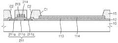
도 3a를 참조하면, 제1박막 트랜지스터(TR1)는 기판(10) 상에 구비된 반도체층(211), 게이트 전극(213, 214), 소스 및 드레인 전극(216)을 포함한다. 상기 도면에는 제1박막 트랜지스터(TR1)의 단면 형상만 도시되어 있으나, 제2박막 트랜지스터(TR2)와 제3박막 트랜지스터(TR3)는 제1박막 트랜지스터(TR1)와 동일한 단면을 가진다.3A, a first thin film transistor TR1 includes a
기판(10) 글라스재 또는 플라스틱재와 같은 다양한 재질로 형성될 수 있다. 단, 기판(10) 측으로 화상이 구현되는 배면 발광형의 경우, 기판(10)은 투명재질로 구비되는 것이 바람직하다. The
상기 도면에는 도시되어 있지 않으나, 기판(10)의 상부에 평활한 면을 형성하고 기판(10) 상부로 불순 원소가 침투하는 것을 차단하기 위하여 기판(10)의 상부에 버퍼층(미도시)을 더 형성할 수 있다. 버퍼층은 SiO2 및/또는 SiNx 등으로 형성할 수 있다.Although not shown in the figure, a buffer layer (not shown) is formed on the top of the
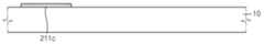
반도체층(211)은 비정질 실리콘 또는 결정질 실리콘을 포함할 수 있으며, 채널 영역(211c)과, 채널 영역(211c) 외측에 이온 불순물이 도핑된 소스 및 드레인 영역(211a)을 포함한다. 소스 및 드레인 영역(211a)은 3족 원소로 도핑하여 p-type, 5족 원소로 도핑하여 n-type 반도체로 형성할 수 있다.The
반도체층(211) 상에는 게이트 절연막인 제1절연층(12)을 사이에 두고 반도체층(211)의 채널 영역(211c)에 대응되는 위치에 제1게이트 전극(213), 및 제2게이트 전극(214)이 차례로 형성된다.The
제1절연층(12)은 반도체층(211)과 제1 및 제2 게이트 전극(213, 214)을 절연하는 것으로 SiNx 및/또는 SiO2와 같은 무기막으로 형성할 수 있다.The first insulating
제1게이트 전극(213)과 제2게이트 전극(214)는 에칭 선택비가 서로 다른 도전물로 구비될 수 있다. 예를 들어, 제1 및 제2 게이트 전극(213,214)는, ITO와 같은 투명도전물, Ti, Mo, Al, Ag, Cu 및 이들의 합금에서 선택된 하나 이상의 에칭 선택비가 다른 물질로 선택될 수 있다. 본 실시예서 제1게이트 전극(213)으로 투명도전물인 ITO가 사용되었고, 제2게이트 전극(214)으로 삼중층의 Mo/Al/Mo이 사용되었다. 한편, 제1게이트 전극(213)의 투명도전물로는 ITO 이외에도 IZO, ZnO 및 In2O3로 이루어지는 군으로부터 선택될 수 있다.The
제1 및 제2 게이트 전극(213, 214) 상에는 제2절연층(15)이 구비된다. 제2절연층(15)은 제1 및 제2게이트 전극(213, 214)과 소스 및 드레인 전극(216)을 절연하는 층간 절연막으로 기능한다.A second insulating
제2절연층(15)은 다양한 절연 물질로 형성할 수 있다. 예를 들어 산화물, 질화물과 같은 무기물로도 형성이 가능하고 유기물로도 형성이 가능하다. 제2절연층(15)을 형성하는 무기 절연막으로는 SiO2, SiNx, SiON, Al2O3, TiO2, Ta2O5, HfO2, ZrO2, BST, PZT 등이 포함될 수 있고, 유기 절연막으로는 일반 범용고분자(PMMA, PS), phenol그룹을 갖는 고분자 유도체, 아크릴계 고분자, 이미드계 고분자, 아릴에테르계 고분자, 아마이드계 고분자, 불소계고분자, p-자일렌계 고분자, 비닐알콜계 고분자 및 이들의 블렌드 등이 포함될 수 있다. 또한, 제2절연층(15)은 무기 절연막과 유기 절연막의 복합 적층체로도 형성될 수 있다.The second insulating
소스 및 드레인 전극(216)이 반도체층(211)의 소스 및 드레인 영역(211a)에 접속한다. 상기 도면에는 소스 및 드레인 전극(216)이 하나의 층으로 도시되어 있으나, 본 발명은 이에 한정되지 않으며 소스 및 드레인 전극(216)은 복수의 층으로 형성될 수 있다.And the source and drain
도 3a를 참조하면, 기판(10) 상에 픽셀부(PXL1)가 구비된다. 픽셀부(PXL1)는 제1화소 전극(113), 발광층(118), 및 대향 전극(119)을 포함한다.Referring to FIG. 3A, a pixel portion PXL1 is provided on a
제1화소 전극(113)은 제1게이트 전극(213)과 동일층에 형성되고, 제1게이트 전극(213)과 동일한 투명도전물로 형성된다. 투명도전물로는 인듐틴옥사이드(indium tin oxide: ITO), 인듐징크옥사이드(indium zink oxide: IZO), 징크옥사이드(zink oxide: ZnO), 인듐옥사이드(indium oxide: In2O3), 인듐갈륨옥사이드(indium galium oxide: IGO), 및 알루미늄징크옥사이드(aluminium zink oxide: AZO)을 포함하는 그룹에서 선택된 적어도 하나 이상을 포함할 수 있다.The
제1화소 전극(113) 상에는 발광층(118)이 형성되고, 발광층(118)에서 방출된 광은 투명도전물로 형성된 제1화소 전극(113)을 통하여 기판(10) 측으로 방출된다.A
제1절연층(12) 및 제1화소 전극(113) 상부에 제3절연층(17)이 형성되고, 제3절연층(17)에는 화소 전극(114) 상부를 노출시키는 개구(C5)가 형성된다. 상기 개구(C5) 내부에 발광층(118)이 구비된다. 발광층(118)은 발광 영역(EL1)을 결정한다.A third insulating
발광층(118)은 저분자 유기물 또는 고분자 유기물일 수 있다. 발광층(118)이 저분자 유기물일 경우, 발광층(118)을 중심으로 홀 수송층(hole transport layer: HTL), 홀 주입층(hole injection layer: HIL), 전자 수송층(electron transport layer: ETL) 및 전자 주입층(electron injection layer: EIL) 등이 적층될 수 있다. 이외에도 필요에 따라 다양한 층들이 적층 될 수 있다. 이때, 사용 가능한 유기 재료로 구리 프탈로시아닌(CuPc: copper phthalocyanine), N'-디(나프탈렌-1-일)-N(N'-Di(naphthalene-1-yl)-N), N'-디페닐-벤지딘(N'-diphenyl-benzidine: NPB), 트리스-8-하이드록시퀴놀린 알루미늄(tris-8-hydroxyquinoline aluminum)(Alq3) 등을 비롯하여 다양하게 적용 가능하다.The
한편, 발광층(118)이 고분자 유기물일 경우, 발광층(118) 외에 홀 수송층(HTL)이 포함될 수 있다. 홀 수송층은 폴리에틸렌 디히드록시티오펜 (PEDOT: poly-(2,4)-ethylene-dihydroxy thiophene)이나, 폴리아닐린(PANI: polyaniline) 등을 사용할 수 있다. 이때, 사용 가능한 유기 재료로 PPV(Poly-Phenylenevinylene)계 및 폴리플루오렌(Polyfluorene)계 등의 고분자 유기물을 사용할 수 있다.On the other hand, when the
발광층(118) 상에는 공통 전극으로 대향 전극(119)이 증착된다. 본 실시예에 따른 유기 발광 표시 장치(1)의 경우, 제1화소 전극(113)은 애노드로 사용되고, 대향 전극(119)은 캐소드로 사용된다. 물론 전극의 극성은 반대로 적용될 수 있음은 물론이다.An
대향 전극(119)은 반사 물질을 포함하는 반사 전극으로 구성될 수 있다. 이때 상기 대향 전극(119)은 Al, Mg, Li, Ca, LiF/Ca, 및 LiF/Al에서 선택된 하나 이상의 물질을 포함할 수 있다. 대향 전극(119)이 반사 전극으로 구비됨으로써, 발광층(118)에서 방출된 빛은 대향 전극(119)에 반사되어 투명도전물로 구성된 제1화소 전극(113)을 투과하여 기판(10) 측으로 방출된다.The
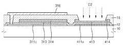
도 3b를 참조하면, 기판(10) 상에 제1커패시터(Cst)가 구비된다.제1커패시터(Cst)는 반도체층(211)과 동일층에 형성된 제1전극(311c), 게이트 전극(213, 214)과 동일층에 형성된 제2전극(313, 314), 및 소스 및 드레인 전극(216)과 동일층에 형성된 제3전극(316)을 포함한다.Referring to FIG. 3B, a first capacitor Cst is provided on the
제1커패시터(Cst)는 회로적으로 전원전압공급 라인(V, 도 1 참조)에 연결되고, 구조적으로 상기 전원전압공급 라인(V)과 중첩되도록 구비된다.The first capacitor Cst is connected to the power supply voltage supply line V (see FIG. 1) in a circuit manner, and structurally overlaps the power supply voltage supply line V.
제1커패시터(Cst)의 제1전극(311c)는 전원전압공급 라인(V)을 따라 그 하부에 위치하고, 반도체층(211)의 채널영역(211c)과 동일한 비정질 반도체 또는 결정질 반도체로 형성된다. 제1커패시터(Cst)의 제1전극(311c)을 구성하는 반도체는 이온 불순물을 포함하지 않는다.The
제1커패시터(Cst)의 제1전극(311c) 상에 제1절연층(12)이 형성되고, 제1절연층(12) 상에 게이트 전극(213, 214)과 동일한 물질인 제2전극(313, 314)이 구비된다. 제2전극의 제1층(313)은 제1게이트 전극(213)과 동일한 투명도전물로 구비되고, 제2전극의 제2층(314)은 제2게이트 전극(214)과 동일한 금속으로 구비된다. 제1커패시터(Cst)의 제2전극(313, 314)도 전술한 전원전압공급 라인(V)을 따라 그 하부에 위치하도록 구비된다. A first insulating
제1커패시터(Cst)의 제2전극(313, 314) 상에 제2절연층(15)이 형성되고, 제2절연층(15) 상에 소스 및 드레인 전극(216)과 동일한 물질을 포함하는 제1커패시터(Cst)의 제3전극(316)이 구비된다. 제3전극(316)은 전원전압공급 라인(V)을 따라 형성된다. 이때, 제3전극(316)은 접속홀(C4)을 통하여 제1전극(311c)과 접속된다. 이로써, 제1커패시터(Cst)는 제1전극(311c)과 제2전극(313, 314) 사이에 형성되는 제1정전용량, 및 제2전극(313, 314)과 제3전극(316) 사이에 형성되는 제2정전용량을 가지는 두 개의 커패시터(Cst1, Cst2, 도 3 참조)가 병렬 연결된다. 따라서, 제1커패시터(Cst)의 정전용량이 증가될 수 있다.The second insulating
전원전압공급 라인(V)은 일반적으로 스캔 라인(S)이나 데이터 라인(D)에 비하여 상대적으로 넓은 폭을 구비하도록 형성되며, 반사율이 높은, 또는 투과율이 낮은 금속으로 형성된다. 본 실시예에 따른 유기 발광 표시 장치(1)의 경우, 제1커패시터(Cst)를 투과율이 낮은 전원전압공급 라인(V)과 중첩되도록 위치시킴으로써, 제1커패시터(Cst)를 전원전압공급 라인(V)에 중첩되지 않는 픽셀 내부의 별도의 영역에 형성하는 경우에 비하여, 유기 발광 표시 장치의 개구율을 향상시킬 수 있다.The power supply voltage supply line V is generally formed to have a relatively wide width as compared with the scan line S or the data line D and is formed of a metal having a high reflectivity or a low transmittance. In the
도 3b를 참조하면, 기판(10) 상에 제2커패시터(Cvth)가 구비된다. 제2커패시터(Cvht)는 반도체층(211)과 동일층에 형성된 제1전극(411a)과, 제1게이트 전극(213)과 동일층에 형성된 제2전극(413)를 포함한다.Referring to FIG. 3B, a second capacitor Cvth is provided on the
제2커패시터(Cvth)의 제1전극(411a)은 박막 트랜지스터의 반도체층(211)과 동일한 물질을 포함한다. 제2커패시터(Cvth)의 제2전극(413)은 제1게이트 전극(213)과 동일한 투명도전물로 형성된다. 특히, 제1전극(411a)은 이온 불순물이 도핑된 반도체물질로 구성됨으로써, 제2전극(413)과 함께 MIM(metal-insulator-metal) CAP 구조를 형성한다.The
MIM CAP 구조는 일반적으로 MOS(Metal Oxide Semiconductor) CAP 구조에 비하여 폭넓은 전압 범위에서 일정한 정전용량을 유지할 수 있다. 따라서, 회로 설계시 전압 설계 마진을 향상시킬 수 있다.The MIM CAP structure is generally capable of maintaining a constant capacitance over a wide voltage range as compared to a MOS (Metal Oxide Semiconductor) CAP structure. Therefore, the voltage design margin can be improved in circuit design.
제1커패시터(Cst)의 제3전극(316) 및 제2커패시터(Cvth)의 제2전극(142) 상에 제3절연층(17)이 형성되고, 제3절연층(170 상에는 공통 전극인 대향 전극(119)이 구비된다.The third insulating
도 4는 본 발명의 비교예에 따른 유기 발광 표시 장치(2)에 포함된 하나의 픽셀을 개략적으로 도시한 평면도로써, 제1커패시터(Cst')가 전원전압공급(V') 라인에 중첩되지 않는 픽셀 내부의 별도 영역에 형성된 경우를 도시한 것이다. 도 5는 도 4의 회로도이고, 도 6a는 도 4의 A'-A'를 따라 취한 단면도이고, 도 6b은 도 4의 B'-B'를 따라 취한 단면도이다.4 is a plan view schematically showing one pixel included in the organic light emitting
도 4를 참조하면, 본 비교예에 따른 유기 발광 표시 장치(2)의 픽셀 내부에는 스캔 라인(S), 데이터 라인(D), 전원전압공급 라인(V'), 보상제어신호 라인(CC)과 같은 복수의 도전 라인들과, 발광 영역(EL2)을 포함하는 픽셀부(PXL2), 제1 내지 제3박막 트랜지스터(TR1, TR2, TR3), 및 제1커패시터(Cst') 및 제2커패시터(Cvth)가 구비된다.Referring to FIG. 4, a scan line S, a data line D, a power supply voltage supply line V ', a compensation control signal line CC, And the first capacitor Cst 'and the second capacitor Cst2 including the light emitting region EL2 and the pixel portion PXL2, the first through third thin film transistors TR1, TR2 and TR3, and the first capacitor Cst' (Cvth).
도 5를 참조하면, 본 비교예에 따른 유기 발광 표시 장치(2)는 저장 커패시터인 제1커패시터(Cst')가 병렬이 아닌 단독으로 구비된다는 점에서, 전술한 본 실시예에 따른 유기 발광 표시 장치(1)와 회로적으로 구별된다.Referring to FIG. 5, in the organic light emitting
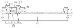
도 6a를 참조하면, 기판(10) 상에 제1박막 트랜지스터(TR1), 제1커패시터(Cst'), 픽셀부(PXL2)가 구비된다. 제1박막 트랜지스터(TR1)는 반도체층(21), 게이트 전극(23, 24), 소스 및 드레인 전극(26)을 포함한다. 픽셀부(PXL2)는 화소 전극(13), 발광층(18), 및 대향 전극(19)을 포함한다.Referring to FIG. 6A, a first thin film transistor TR1, a first capacitor Cst ', and a pixel portion PXL2 are provided on a
화소 전극(13)은 제1게이트 전극(23)과 동일층에 형성되고, 제1게이트 전극(23)과 동일한 투명도전물로 형성된다. 화소 전극(13) 상에는 발광층(18)이 형성되고, 발광층(18)에서 방출된 광은 투명도전물로 형성된 제1화소 전극(13)을 통하여 기판(10) 측으로 방출된다.The
픽셀부(PXL2)와 제1박막 트랜지스터(TR1) 사이에 저장 커패시터인 제1커패시터(Cst')가 구비된다. 비교예의 제1커패시터(Cst')는 반도체층(21)과 동일층에 형성된 제1전극(51a)과, 게이트 전극(23, 24)과 동일층에 형성된 제2전극(53)을 포함한다. 이때, 제1전극(51a)은 이온 불순물이 도핑된 반도체물질로 구성됨으로써, 제2전극(53)과 함께 MIM CAP 구조가 된다. 이와 같은 MIM CAP 구조는 전체적으로 투과율이 낮아 발광층(18)에서 방출된 빛이 투과되기 어렵다. 따라서, 발광층(18)에 의해 결정되는 발광영역(EL2)이 전술한 본 발명의 일 실시예에 따른 유기 발광 표시 장치(1)의 발광영역(EL1)보다 좁아진다. 결과적으로 개구율이 저하된다.A first capacitor Cst ', which is a storage capacitor, is provided between the pixel portion PXL2 and the first thin film transistor TR1. The first capacitor Cst 'of the comparative example includes a
도 6b를 참조하면, 기판(10) 상에 전원전압공급 라인(V)과 제2커패시터(Cvth)가 구비된다.Referring to FIG. 6B, a power supply voltage supply line V and a second capacitor Cvth are provided on a
전원전압공급 라인(V')은 제1절연층(12) 상에 제1게이트 전극(13)과 동일한 물질로 형성된 제1층(33), 및 제2게이트 전극(14)과 동일한 물질로 형성된 제2층(34)을 포함한다. 제1층(33) 및 제2층(34) 상에 제2절연층(15)이 구비되고, 제2절연층(15) 상에 소스 및 드레인 전극(26)과 동일한 물질로 형성된 제3층(36)을 포함한다.The power source voltage supply line V 'includes a
제2커패시터(Cvht)는 반도체층(21)과 동일층에 형성된 제1전극(41a)과, 제1게이트 전극(23)과 동일층에 형성된 제2전극(43)를 포함한다. 제2커패시터(Cvth)의 제1전극(41a)은 박막 트랜지스터의 반도체층(21)과 동일한 물질을 포함한다. 제2커패시터(Cvth)의 제2전극(43)은 제1게이트 전극(23)과 동일한 투명도전물로 형성된다. 특히, 제1전극(41a)은 이온 불순물이 도핑된 반도체물질로 구성됨으로써, 제2전극(43)과 함께 MIM CAP 구조를 형성한다.The second capacitor Cvht includes a
따라서, 본 비교예에 따른 유기 발광 표시 장치(2)는 제1커패시터(Cst')가 전원전압공급 라인(V')과 중첩되지 않는 픽셀 내부의 별도 영역에 형성되기 때문에, 발광층(18)에 의해 결정되는 발광 영역(EL2)이 형성되는 면적이 좁다. 따라서 개구율이 낮아진다.
Therefore, since the organic light emitting
이하, 도 7a 내지 도 11b를 참조하여 본 발명의 일 실시예에 따른 유기 발광 표시 장치(1)의 제조 방법을 설명한다.Hereinafter, a method of manufacturing the organic light emitting
도 7a 및 7b은 본 발명의 일 실시예에 따른 유기 발광 표시 장치(1)의 제1마스크 공정의 결과를 개략적으로 도시한 단면도이다.7A and 7B are cross-sectional views schematically showing the result of the first mask process of the organic light emitting
도 7a를 참조하면, 기판(10) 상에 제1박막 트랜지스터의 반도체층(211)이 형성되고, 도 7b를 참조하면 기판(10) 상에 제1커패시터(Cst)의 제1전극(311c) 및 제2커패시터(Cvth)의 제1전극(411c)이 형성된다.7A, a
상기 도면에는 도시되어 있지 않지만, 기판(10) 상에는 반도체층 형성 물질(미도시)이 증착되고, 반도체층 형성 물질(미도시) 상에 포토레지스터(미도시)가 도포된다. 제1포토마스크(미도시)를 이용한 포토리소그라피 공정에 의해 반도체층 형성 물질(미도시)이 패터닝되어, 제1박막 트랜지스터(TR1)의 반도체층(211), 및 제1커패시터(Cst)의 제1전극(311c) 및 제2커패시터(Cvth)의 제1전극(411c)이 동시에 형성된다. 상기 도면에는 도시되어 있지만, 제2박막 트랜지스터(TR2), 및 제3박막 트랜지스터(TR3)도 제1박막 트랜지스터(TR1)와 동일하게 형성된다.Although not shown in the figure, a semiconductor layer forming material (not shown) is deposited on the
포토리소그라피에 의한 제1마스크 공정은 제1포토마스크(미도시)에 노광장치(미도시)로 노광 후, 현상(developing), 식각(etching), 및 스트립핑(stripping) 또는 에싱(ashing) 등과 같은 일련의 공정을 거쳐 진행된다.The first mask process by photolithography is a process of exposing the first photomask (not shown) with an exposure apparatus (not shown), developing, etching, stripping or ashing The same series of processes are carried out.
반도체층(211)은 비정질 실리콘(amorphous silicon) 또는 결정질 실리콘(poly silicon)으로 구비될 수 있다. 이때, 결정질 실리콘은 비정질 실리콘을 결정화하여 형성될 수도 있다. 비정질 실리콘을 결정화하는 방법은 RTA(rapid thermal annealing)법, SPC(solid phase crystallzation)법, ELA(excimer laser annealing)법, MIC(metal induced crystallzation)법, MILC(metal induced lateral crystallzation)법, SLS(sequential lateral solidification)법 등 다양한 방법에 의해 결정화될 수 있다. ]The
도 8a 및 8b은 본 발명의 일 실시예에 따른 유기 발광 표시 장치(1)의 제2마스크 공정의 결과를 개략적으로 도시한 단면도이다.8A and 8B are cross-sectional views schematically showing the result of the second mask process of the organic light emitting
도 8a를 참조하면, 도 7a의 제1마스크 공정의 결과물 상에 제1절연층(12)이 적층되고, 제1절연층(12) 상에 제1게이트 전극(213) 및 제2게이트 전극(214)이 순차로 적층되고, 픽셀부(PXL1)에 제1화소 전극(113) 및 제2화소 전극(114)이 순차로 적층된다.Referring to FIG. 8A, a first insulating
도 8b를 참조하면, 도 7b의 제1마스크 공정의 결과물 상에 제1절연층(12) 이 형성되고, 제1절연층(12) 상에 제1커패시터(Cst)의 제2전극의 제1층(313) 및 제2층(314)이 순차로 적층되고, 제2커패시터(Cvth)의 제2전극의 제1층(413) 및 제2층(414)이 순차로 적층된다.Referring to FIG. 8B, a first insulating
제1게이트 전극(213), 제1화소 전극(113), 제1커패시터(Cst)의 제2전극의 제1층(313) 및 제2커패시터(Cvth)의 제2전극의 제1층(413)은 동일층에 동시에 형성되고, ITO, IZO, ZnO 및 In2O3로 이루어지는 군으로부터 선택될 수 있는 동일한 투명도전물로 형성된다.The
제2게이트 전극(214), 제2화소 전극(114), 제1커패시터(Cst)의 제2전극의 제2층(314) 및 제2커패시터(Cvth)의 제2전극의 제2층(414)은 동일층에 동시에 형성되고, Ti, Mo, Al, Ag, Cu 및 이들의 합금에서 선택된 하나 이상의 재료로 형성될 수 있다.The
상기와 같은 구조물 위에 이온 불순물을 도핑(D1)한다. 이온 불순물은 전술한 바와 같이 3족 또는 5족의 이온으로 도핑할 수 있으며, 1ㅧ1015 atoms/㎠ 이상의 농도로 박막 트랜지스터의 반도체층(211)을 타겟으로 하여 도핑한다.An ionic impurity is doped (D1) on the structure as described above. The ionic impurities can be doped with Group 3 or Group 5 ions as described above, and the
이때, 제1 및 제2게이트 전극(213, 214)을 셀프 얼라인(self align) 마스크로 사용하여 반도체층(211)에 이온 불순물을 도핑함으로써 반도체층(211)은 이온 불순물이 도핑된 소스 및 드레인 영역(212a)과, 그 사이에 채널 영역(212c)을 구비하게 된다. 즉, 제1 및 제2게이트 전극(213, 214)을 셀프 얼라인 마스크로 사용함으로써, 별도의 포토 마스크를 추가하지 않고 소스 및 드레인 영역(212a)을 형성할 수 있다. The
도 9a 및 9b은 본 발명의 일 실시예에 따른 유기 발광 표시 장치(1)의 제3마스크 공정의 결과를 개략적으로 도시한 단면도이다.9A and 9B are cross-sectional views schematically showing the result of a third mask process of the organic light emitting
도 9a 및 9b를 참조하면, 도 8a 및 8b의 제2마스크 공정의 결과물 상에 제2절연층(15)이 적층되고, 제2절연층(15)을 패터닝하여 제2화소 전극(114)의 상부를 노출시키는 제1콘택홀(C1), 반도체층(211)의 소스 및 드레인 영역(211a)의 일부를 노출시키는 제2콘택홀(C2), 제2커패시터(Cvth)의 제2전극의 제2층(314)의 상부를 노출시키는 제3콘택홀(C3), 및 제1커패시터(Cst)의 제1전극(311c)의 일부를 노출시키는 제4콘택홀(C4)이 형성된다.9A and 9B, a second insulating
도 10a 및 10b은 본 발명의 일 실시예에 따른 유기 발광 표시 장치(1)의 제4마스크 공정의 결과를 개략적으로 도시한 단면도이다.10A and 10B are cross-sectional views schematically showing the results of a fourth mask process of the organic light emitting
도 10a를 참조하면, 도 9a의 제3마스크 공정의 결과물 상에, 소스 및 드레인 영역(211a)에 각각 접속하는 소스 및 드레인 전극(216)이 형성되고, 픽셀부(PXL1)의 제2화소 전극(114)이 제거된다.Referring to FIG. 10A, source and drain
도 10b를 참조하면, 도 9b의 제3마스크 공정의 결과물 상에, 제1커패시터(Cst)의 제1전극(311c)에 접속하는 제1커패시터(Cst)의 제3전극(316)이 형성되고, 제2커패시터(Cvth)의 제2전극의 제2층(414)이 제거된다.Referring to FIG. 10B, a
상기 제4마스크 공정은 제2화소 전극(114) 및 제2커패시터(Cvth)의 제2전극의 제2층(414) 상에 적층된 소스 및 드레인 전극(216)을 형성하는 도전물을 식각하는 제1식각 공정과, 제1식각 공정 후 제2화소 전극(114) 및 제2커패시터(Cvth)의 제2전극의 제2층(414)을 제거하는 제2식각 공정을 포함할 수 있다. 식각 공정의 분리는 제2화소 전극(114) 및 제2커패시터(Cvth)의 제2전극의 제2층(414)을 형성하는 재료와 소스 및 드레인 전극(216)의 재료가 이종 일 때 바람직하며, 만약 제2화소 전극(114) 및 제2커패시터(Cvth)의 제2전극의 제2층(414)을 형성하는 재료와 소스 및 드레인 전극(216)의 재료가 동종인 경우에는 한번의 식각 공정이 가능함은 물론이다.The fourth masking process etches the conductive material forming the source and drain
제4마스크 공정 후, 상기와 같은 구조물 위에 이온 불순물을 도핑(D2)한다. 이온 불순물은 전술한 바와 같이 3족 또는 5족의 이온으로 도핑할 수 있으며, 1×10¹⁵ atoms/㎠ 이상의 농도로 제2커패시터(Cvth)의 제1전극(411c) 을 타겟으로 하여 도핑한다.After the fourth mask process, ion impurities are doped (D2) on the structure as described above. The ionic impurities can be doped with Group 3 or Group 5 ions as described above, and the
제2커패시터(Cvth)의 제2전극의 제1층(413)은 두께가 1000Å 이하로 얇게 형성되기 때문에 이온 불순물은 제1층(413)을 통과하여 제1전극(411c)에 도핑된다. 그 결과 이온 불순물이 도핑된 제1전극(411a)은 제2커패시터(Cvht)의 제2전극의 제2층(413)과 함께 MIM CAP 구조를 형성하므로 회로 설계시 전압 설계 마진을 향상시킬 수 있다.Since the
한편, 제1커패시터(Cst)의 제1전극(311c)은, 제1전극(311c) 상부에 상당한 두께로 형성된 제2전극의 제2층(314) 및 제3전극(316)이 차단막으로 기능하여 이온 불순물이 도핑되지 않는다.The
도 11a 및 11b은 본 발명의 일 실시예에 따른 유기 발광 표시 장치(1)의 제5마스크 공정의 결과를 개략적으로 도시한 단면도이다.11A and 11B are cross-sectional views schematically showing the result of the fifth mask process of the organic light emitting
도 11a 및 11b를 참조하면, 도 10a 및 10b의 제4마스크 공정의 결과물 상에 제3절연층(17)을 형성하고, 제1화소 전극(113)의 상면을 노출시키는 개구(C5)를 형성한다.11A and 11B, a third insulating
개구(C5) 내부에 전술한 발광층(118, 도 3a 참조)이 구비됨으로써, 제1화소 전극(113) 및 대향 전극(119, 도 3a 참조)의 전압 인가에 의해 발광층(118)이 발광한다. 따라서, 발광 영역(EL1)이 확대되어 개구율을 증가시킬 수 있다.The
본 발명은 도면에 도시된 실시 예를 참고로 설명되었으나 이는 예시적인 것에 불과하며, 당해 기술 분야에서 통상의 지식을 가진 자라면 이로부터 다양한 변형 및 균등한 다른 실시 예가 가능하다는 점을 이해할 것이다. 따라서, 본 발명의 진정한 기술적 보호 범위는 첨부된 특허청구범위의 기술적 사상에 의하여 정해져야 할 것이다.While the present invention has been described with reference to exemplary embodiments, it is to be understood that the invention is not limited to the disclosed exemplary embodiments, but, on the contrary, is intended to cover various modifications and equivalent arrangements included within the spirit and scope of the invention. Accordingly, the true scope of the present invention should be determined by the technical idea of the appended claims.
1: 유기 발광 표시 장치
10: 기판12: 제1절연층
15: 제2절연층17: 제3절연층
113: 제1화소 전극114: 제2화소 전극
118: 발광층119: 대향 전극
211: 반도체층211a: 소스 및 드레인 영역
211c: 채널 영역213: 제1게이트 전극
214: 제2게이트 전극216: 소스 및 드레인 전극
311a: 제1커패시터의 제1전극
313: 제1커패시터의 제2전극 제1층
314: 제1커패시터의 제2전극 제2층
316: 제1커패시터의 제3전극
411a: 제2커패시터의 제1전극
413: 제2커패시터의 제2전극 제1층
414: 제2커패시터의 제2전극 제2층
S: 스캔 라인D: 데이터 라인
V: 전원전압공급 라인CC: 보상제어신호 라인
PXL1: 픽셀부TR1~TR3: 박막 트랜지스터
Cst: 제1커패시터Cvth: 제2커패시터
C1~C5: 콘택홀1: organic light emitting display
10: substrate 12: first insulating layer
15: second insulation layer 17: third insulation layer
113: first pixel electrode 114: second pixel electrode
118: luminescent layer 119: counter electrode
211:
211c: channel region 213: first gate electrode
214: second gate electrode 216: source and drain electrodes
311a: a first electrode of the first capacitor
313: second electrode of the first capacitor [
314: second electrode of the first capacitor second layer
316: a third electrode of the first capacitor
411a: a first electrode of the second capacitor
413: second electrode of the second capacitor [
414: second electrode of the second capacitor second layer
S: scan line D: data line
V: Power supply voltage supply line CC: Compensation control signal line
PXL1: Pixel part TR1 to TR3: Thin film transistor
Cst: first capacitor Cvth: second capacitor
C1 to C5: Contact holes
Claims (21)
Translated fromKorean상기 반도체층과 동일층에 형성되고 이온 불순물이 도핑되지 않은 반도체를 포함하는 제1전극, 상기 게이트 전극과 동일층에 형성된 제2전극, 및 상기 소스 및 드레인 전극과 동일층에 형성된 제3전극이 구비된 제1커패시터;
상기 반도체층과 동일층에 형성되고 도핑된 이온 불순물을 포함하는 제1전극, 및 상기 게이트 전극과 동일층에 형성된 제2전극이 구비된 제2커패시터;
상기 게이트 전극과 동일층에 형성되고, 상기 트랜지스터에 전기적으로 연결된 화소 전극;
상기 화소 전극 상에 위치하는 발광층; 및
상기 발광층을 사이에 두고 상기 화소 전극에 대향 배치되는 대향 전극;을 포함하고,
상기 제2커패시터의 제2전극은 제1층, 및 상기 제1층의 상면에 위치하고 상기 제1층의 상면 중앙부를 오픈하는 개구를 구비한 제2층을 포함하고,
상기 제2커패시터의 제1전극에 형성된 이온 불순물은 상기 개구에 대응하는 영역에 위치하는 유기 발광 표시 장치.At least one transistor having a semiconductor layer, a gate electrode, and source and drain electrodes;
A second electrode formed on the same layer as the gate electrode, and a third electrode formed on the same layer as the source and drain electrodes, the first electrode including a semiconductor formed on the same layer as the semiconductor layer and not doped with ionic impurities, A first capacitor;
A second capacitor formed on the same layer as the semiconductor layer and including a first electrode including a doped ion impurity and a second electrode formed on the same layer as the gate electrode;
A pixel electrode formed on the same layer as the gate electrode and electrically connected to the transistor;
A light emitting layer disposed on the pixel electrode; And
And a counter electrode disposed opposite to the pixel electrode with the light emitting layer interposed therebetween,
Wherein the second electrode of the second capacitor comprises a first layer and a second layer located on the top surface of the first layer and having an opening that opens the center of the top surface of the first layer,
Wherein an ion impurity formed in the first electrode of the second capacitor is located in a region corresponding to the opening.
상기 제1커패시터는 상기 적어도 하나의 트랜지스터에 전원 전압을 공급하는 전원 전압 공급선과 연결되고, 상기 전원 전압 공급선과 중첩되도록 위치하는 유기 발광 표시 장치.The method according to claim 1,
Wherein the first capacitor is connected to a power supply voltage supply line for supplying a power supply voltage to the at least one transistor and is positioned to overlap the power supply voltage supply line.
상기 적어도 하나의 트랜지스터는 구동 트랜지스터이고, 상기 제1커패시터는 상기 구동 트랜지스터에 전압을 인가하는 저장 커패시터인 유기 발광 표시 장치.3. The method of claim 2,
Wherein the at least one transistor is a driving transistor, and the first capacitor is a storage capacitor for applying a voltage to the driving transistor.
상기 제1커패시터의 제1전극과 제3전극은 접속홀을 통하여 연결된 유기 발광 표시 장치.The method according to claim 1,
Wherein the first electrode and the third electrode of the first capacitor are connected to each other through a connection hole.
상기 제1커패시터는 상기 제1전극과 상기 제2전극 사이에 형성된 제1정전용량, 및 상기 제2전극과 상기 제3전극 사이에 형성된 제2정전용량이 병렬 연결된 유기 발광 표시 장치.6. The method of claim 5,
The first capacitor has a first capacitance formed between the first electrode and the second electrode, and a second capacitance formed between the second electrode and the third electrode in parallel.
상기 제1커패시터의 제2전극은 상기 게이트 전극과 동일한 물질을 포함하는 유기 발광 표시 장치.The method according to claim 1,
Wherein the second electrode of the first capacitor includes the same material as the gate electrode.
상기 제1커패시터의 제3전극은 상기 소스 및 드레인 전극과 동일한 물질을 포함하는 유기 발광 표시 장치.The method according to claim 1,
And the third electrode of the first capacitor includes the same material as the source and drain electrodes.
상기 제1커패시터의 제3전극은 상기 적어도 하나의 트랜지스터에 전원 전압을 공급하는 전원 전압 공급선을 포함하는 유기 발광 표시 장치.9. The method of claim 8,
And a third electrode of the first capacitor includes a power supply voltage supply line for supplying a power supply voltage to the at least one transistor.
상기 제2커패시터는 구동 트랜지스터의 게이트 단자에 연결된 보상 커패시터인 유기 발광 표시 장치.The method according to claim 1,
And the second capacitor is a compensation capacitor connected to the gate terminal of the driving transistor.
상기 제2커패시터의 제2전극은 투명도전물인 유기 발광 표시 장치.The method according to claim 1,
And the second electrode of the second capacitor is a transparent conductive material.
상기 게이트 전극은 투명도전물을 포함하는 제1층, 및 금속을 포함하는 제2층으로 구비된 유기 발광 표시 장치.The method according to claim 1,
Wherein the gate electrode comprises a first layer including a transparent conductive material and a second layer including a metal.
상기 화소 전극은 상기 게이트 전극의 투명도전물로 구비된 유기 발광 표시 장치.The method according to claim 1,
And the pixel electrode is provided as a transparent conductive material of the gate electrode.
상기 반도체층은 비정질 실리콘 또는 결정질 실리콘인 유기 발광 표시 장치.The method according to claim 1,
Wherein the semiconductor layer is amorphous silicon or crystalline silicon.
상기 대향 전극은 상기 발광층에서 방출된 광을 반사하는 반사 전극인 유기 발광 표시 장치.The method according to claim 1,
And the counter electrode is a reflective electrode that reflects light emitted from the light emitting layer.
제1마스크 공정의 결과물 상에 제1절연층을 형성하고, 상기 제1절연층 상에 투명도전물 및 제1금속을 차례로 형성하고 이를 패터닝하여, 트랜지스터의 게이트 전극, 화소 전극, 제1 및 제2커패시터의 제2전극을 형성하는 제2마스크 공정;
제2마스크 공정의 결과물 상에 제2절연층을 형성하고, 상기 반도체층의 소스 및 드레인 영역, 상기 화소 전극, 상기 제1커패시터의 제1전극 일부, 및 상기 제2커패시터의 제2전극을 노출시키는 콘택홀들을 형성하는 제3마스크 공정;
제3마스크 공정의 결과물 상에 제2금속을 형성하고, 상기 제2금속을 패터닝하여 상기 소스 및 드레인 영역과 접속하는 소스 및 드레인 전극, 및 상기 제1커패시터의 제3전극을 형성하는 제4마스크 공정; 및
제4마스크 공정의 결과물 상에 제3절연층을 형성하고, 상기 화소 전극의 투명도전물이 노출되도록 제3절연층을 개구시키는 제5마스크 공정;을 포함하는 유기 발광 표시 장치의 제조 방법.A first masking step of forming a semiconductor layer on a substrate and patterning the semiconductor layer to form a semiconductor layer of the transistor and a first electrode of the first and second capacitors;
Forming a first insulating layer on the result of the first mask process, sequentially forming a transparent conductive material and a first metal on the first insulating layer, and patterning the same to form a gate electrode, a pixel electrode, A second mask process for forming a second electrode of the second capacitor;
Forming a second insulating layer on the result of the second mask process, exposing the source and drain regions of the semiconductor layer, the pixel electrode, a first electrode portion of the first capacitor, and a second electrode of the second capacitor, A third masking step of forming contact holes to expose the contact holes;
Forming a second metal on the resultant of the third masking process, patterning the second metal to form source and drain electrodes connected to the source and drain regions, and forming a third electrode of the first capacitor, fair; And
And a fifth masking step of forming a third insulating layer on the result of the fourth masking step and opening the third insulating layer to expose the transparent conductive material of the pixel electrode.
상기 제2마스크 공정 후, 상기 소스 및 드레인 영역에 이온 불순물을 도핑하는 유기 발광 표시 장치의 제조 방법.17. The method of claim 16,
And ion doping is doped into the source and drain regions after the second mask process.
상기 제4마스크 공정은, 상기 화소 전극 및 제2커패시터의 제2전극 상에 적층된 상기 제2금속을 제거하는 제1식각 공정, 상기 화소 전극 및 제2커패시터의 투명도전물 상에 형성된 상기 제1금속을 제거하는 제2식각 공정을 포함하는 유기 발광 표시 장치의 제조 방법.17. The method of claim 16,
The fourth mask process may include a first etching process for removing the second metal stacked on the second electrode of the pixel electrode and the second capacitor, a second etching process for removing the second metal stacked on the second electrode of the pixel capacitor and the second capacitor, 1 < / RTI >metal; and a second etching process for removing the metal.
상기 제4마스크 공정에서, 상기 제2금속은 상기 제1금속과 동일 재료로 형성되고, 상기 제1금속 및 제2금속을 동시에 식각하는 유기 발광 표시 장치의 제조 방법.17. The method of claim 16,
In the fourth mask process, the second metal is formed of the same material as the first metal, and the first metal and the second metal are simultaneously etched.
상기 제4마스크 공정 후, 상기 제2커패시터의 제1전극에 이온 불순물을 도핑하는 유기 발광 표시 장치의 제조 방법.17. The method of claim 16,
After the fourth mask process, the first electrode of the second capacitor is doped with an ionic impurity.
상기 제5마스크 공정 후, 상기 화소 전극 상부에 발광층, 및 대향 전극을 더 형성하는 유기 발광 표시 장치의 제조 방법.17. The method of claim 16,
Wherein a light emitting layer and an opposite electrode are further formed on the pixel electrode after the fifth mask process.
Priority Applications (4)
| Application Number | Priority Date | Filing Date | Title |
|---|---|---|---|
| KR1020100127856AKR101736319B1 (en) | 2010-12-14 | 2010-12-14 | Organic light emitting display device and manufacturing method of the same |
| US13/208,163US9123594B2 (en) | 2010-12-14 | 2011-08-11 | Organic light-emitting display apparatus having high aperture ratio |
| TW100139871ATWI584456B (en) | 2010-12-14 | 2011-11-01 | Organic light emitting display device and method of manufacturing same |
| CN201110414220.5ACN102569343B (en) | 2010-12-14 | 2011-12-13 | Organic light-emitting display device and manufacture method thereof |
Applications Claiming Priority (1)
| Application Number | Priority Date | Filing Date | Title |
|---|---|---|---|
| KR1020100127856AKR101736319B1 (en) | 2010-12-14 | 2010-12-14 | Organic light emitting display device and manufacturing method of the same |
Publications (2)
| Publication Number | Publication Date |
|---|---|
| KR20120066491A KR20120066491A (en) | 2012-06-22 |
| KR101736319B1true KR101736319B1 (en) | 2017-05-17 |
Family
ID=46198418
Family Applications (1)
| Application Number | Title | Priority Date | Filing Date |
|---|---|---|---|
| KR1020100127856AActiveKR101736319B1 (en) | 2010-12-14 | 2010-12-14 | Organic light emitting display device and manufacturing method of the same |
Country Status (4)
| Country | Link |
|---|---|
| US (1) | US9123594B2 (en) |
| KR (1) | KR101736319B1 (en) |
| CN (1) | CN102569343B (en) |
| TW (1) | TWI584456B (en) |
Cited By (1)
| Publication number | Priority date | Publication date | Assignee | Title |
|---|---|---|---|---|
| KR20160069369A (en)* | 2014-12-08 | 2016-06-16 | 엘지디스플레이 주식회사 | Display device having bridge line and method for fabricaging the same |
Families Citing this family (28)
| Publication number | Priority date | Publication date | Assignee | Title |
|---|---|---|---|---|
| KR101930845B1 (en) | 2011-08-09 | 2018-12-20 | 삼성디스플레이 주식회사 | Thin-film transistor array substrate, organic light emitting display device comprising the same and manufacturing method of the same |
| KR101486038B1 (en) | 2012-08-02 | 2015-01-26 | 삼성디스플레이 주식회사 | Organic light emitting diode display |
| KR101971925B1 (en) | 2012-09-19 | 2019-08-19 | 삼성디스플레이 주식회사 | Substrate formed thin film transistor array and organic light emitting diode display |
| JP6083089B2 (en)* | 2013-03-27 | 2017-02-22 | 株式会社Joled | Semiconductor device, display device and electronic apparatus |
| KR102143924B1 (en)* | 2013-07-12 | 2020-08-13 | 삼성디스플레이 주식회사 | Organic light emitting diode display |
| KR102108358B1 (en)* | 2013-08-28 | 2020-05-11 | 삼성디스플레이 주식회사 | Method for repairing organic light emitting display apparatus |
| KR102253870B1 (en)* | 2014-08-11 | 2021-05-21 | 삼성디스플레이 주식회사 | Organic light emitting display device |
| KR102373536B1 (en) | 2015-01-27 | 2022-03-11 | 삼성디스플레이 주식회사 | Circle display and driving method thereof |
| CN104576708B (en)* | 2015-01-28 | 2017-05-03 | 深圳市华星光电技术有限公司 | OLED (organic light-emitting diode) pixel structure |
| TWI549265B (en)* | 2015-02-11 | 2016-09-11 | 友達光電股份有限公司 | Pixel structure and its manufacturing method |
| KR102500271B1 (en)* | 2015-08-19 | 2023-02-16 | 삼성디스플레이 주식회사 | Organic light emitting display apparatus and method for manufacturing the same |
| CN106775039B (en)* | 2015-11-20 | 2024-02-02 | 京东方科技集团股份有限公司 | Embedded touch screen, manufacturing method thereof and display device |
| KR102651136B1 (en)* | 2016-04-12 | 2024-03-25 | 삼성디스플레이 주식회사 | Organic light emitting diode display and method for manufacturing the same |
| CN108231790B (en) | 2016-12-13 | 2019-09-17 | 昆山工研院新型平板显示技术中心有限公司 | Display device and its manufacturing method |
| KR102571610B1 (en) | 2017-02-13 | 2023-08-30 | 삼성디스플레이 주식회사 | Semiconductor device and method for fabricating the same |
| KR102448095B1 (en)* | 2017-09-08 | 2022-09-29 | 삼성디스플레이 주식회사 | Display device, manufacturing method of display device, and electrode building method |
| CN107785407B (en)* | 2017-11-14 | 2021-08-03 | 京东方科技集团股份有限公司 | An OLED display panel and display device |
| KR102034692B1 (en)* | 2019-04-17 | 2019-10-22 | 삼성디스플레이 주식회사 | Substrate formed thin film transistor array and organic light emitting diode display |
| KR102845725B1 (en)* | 2019-09-26 | 2025-08-14 | 삼성디스플레이 주식회사 | Display device |
| KR102070953B1 (en)* | 2019-10-14 | 2020-01-30 | 삼성디스플레이 주식회사 | Substrate formed thin film transistor array and organic light emitting diode display |
| KR102107110B1 (en)* | 2020-01-17 | 2020-05-07 | 삼성디스플레이 주식회사 | Substrate formed thin film transistor array and organic light emitting diode display |
| KR102169019B1 (en)* | 2020-04-24 | 2020-10-23 | 삼성디스플레이 주식회사 | Substrate formed thin film transistor array and organic light emitting diode display |
| KR102307503B1 (en)* | 2020-04-24 | 2021-10-01 | 삼성디스플레이 주식회사 | Substrate formed thin film transistor array and organic light emitting diode display |
| CN111383600B (en)* | 2020-04-28 | 2022-04-19 | 厦门天马微电子有限公司 | Pixel driving circuit, driving method, display panel and display device |
| CN115398530B (en) | 2021-01-26 | 2024-12-27 | 京东方科技集团股份有限公司 | Shifting register unit and driving method thereof, grid driving circuit and display substrate |
| CN115606000A (en)* | 2021-01-26 | 2023-01-13 | 京东方科技集团股份有限公司(Cn) | Display substrate, manufacturing method thereof, and display device |
| GB2610339A (en)* | 2021-01-29 | 2023-03-01 | Boe Technology Group Co Ltd | Array substrate and display apparatus |
| CN113178469B (en)* | 2021-04-22 | 2023-10-27 | 厦门天马微电子有限公司 | Display panel and display device |
Family Cites Families (14)
| Publication number | Priority date | Publication date | Assignee | Title |
|---|---|---|---|---|
| TW321731B (en)* | 1994-07-27 | 1997-12-01 | Hitachi Ltd | |
| US6909233B2 (en)* | 2003-06-11 | 2005-06-21 | Eastman Kodak Company | Stacked OLED display having improved efficiency |
| KR100627284B1 (en) | 2004-05-25 | 2006-09-25 | 삼성에스디아이 주식회사 | Organic light emitting display panel |
| JP4549889B2 (en) | 2004-05-24 | 2010-09-22 | 三星モバイルディスプレイ株式會社 | Capacitor and light-emitting display device using the same |
| KR101107252B1 (en)* | 2004-12-31 | 2012-01-19 | 엘지디스플레이 주식회사 | Thin film transistor substrate of electroluminescent display panel and manufacturing method thereof |
| KR100635509B1 (en) | 2005-08-16 | 2006-10-17 | 삼성에스디아이 주식회사 | Organic electroluminescent display |
| KR100823199B1 (en)* | 2007-04-05 | 2008-04-18 | 삼성에스디아이 주식회사 | Organic light emitting display |
| KR100867926B1 (en)* | 2007-06-21 | 2008-11-10 | 삼성에스디아이 주식회사 | Organic light emitting display device and manufacturing method thereof |
| KR100908236B1 (en)* | 2008-04-24 | 2009-07-20 | 삼성모바일디스플레이주식회사 | OLED display device and manufacturing method thereof |
| KR100964227B1 (en)* | 2008-05-06 | 2010-06-17 | 삼성모바일디스플레이주식회사 | Thin film transistor array substrate for flat panel display, organic light emitting display device comprising same, and manufacturing method thereof |
| KR20100054433A (en) | 2008-11-14 | 2010-05-25 | 삼성전자주식회사 | Organic light emitting device and manufacturing method thereof |
| US8193695B2 (en) | 2008-07-17 | 2012-06-05 | Samsung Electronics Co., Ltd. | Organic light emitting device and manufacturing method thereof |
| KR101074788B1 (en)* | 2009-01-30 | 2011-10-20 | 삼성모바일디스플레이주식회사 | Flat panel display apparatus and the manufacturing method thereof |
| KR101048987B1 (en)* | 2009-12-10 | 2011-07-12 | 삼성모바일디스플레이주식회사 | Flat panel display and manufacturing method thereof |
- 2010
- 2010-12-14KRKR1020100127856Apatent/KR101736319B1/enactiveActive
- 2011
- 2011-08-11USUS13/208,163patent/US9123594B2/enactiveActive
- 2011-11-01TWTW100139871Apatent/TWI584456B/enactive
- 2011-12-13CNCN201110414220.5Apatent/CN102569343B/enactiveActive
Cited By (2)
| Publication number | Priority date | Publication date | Assignee | Title |
|---|---|---|---|---|
| KR20160069369A (en)* | 2014-12-08 | 2016-06-16 | 엘지디스플레이 주식회사 | Display device having bridge line and method for fabricaging the same |
| KR102345132B1 (en) | 2014-12-08 | 2021-12-29 | 엘지디스플레이 주식회사 | Display device having bridge line and method for fabricaging the same |
Also Published As
| Publication number | Publication date |
|---|---|
| TW201227952A (en) | 2012-07-01 |
| TWI584456B (en) | 2017-05-21 |
| CN102569343A (en) | 2012-07-11 |
| CN102569343B (en) | 2016-01-20 |
| KR20120066491A (en) | 2012-06-22 |
| US9123594B2 (en) | 2015-09-01 |
| US20120146004A1 (en) | 2012-06-14 |
Similar Documents
| Publication | Publication Date | Title |
|---|---|---|
| KR101736319B1 (en) | Organic light emitting display device and manufacturing method of the same | |
| KR101802860B1 (en) | Organic light emitting display device and manufacturing method of the same | |
| KR101822563B1 (en) | Organic light emitting display device and manufacturing method of the same | |
| KR101372852B1 (en) | Organic light emitting display device and manufacturing method of the same | |
| KR101837625B1 (en) | Organic light emitting display device and the method of manufacturing the same | |
| KR101833235B1 (en) | Thin-film transistor array substrate, organic light emitting display device comprising the same and manufacturing method of the same | |
| US8866145B2 (en) | Organic light-emitting display device including an insulating layer having different thicknesses | |
| KR101880720B1 (en) | Thin-film transistor array substrate, organic light emitting display device comprising the same and manufacturing method of the same | |
| KR101925540B1 (en) | Thin-film transistor array substrate, organic light emitting display device comprising the same and manufacturing method of the same | |
| KR101954984B1 (en) | Thin-film transistor array substrate, organic light emitting display device comprising the same and manufacturing method of the same | |
| KR102078356B1 (en) | Organic light emitting display apparatus and manufacturing method thereof | |
| KR101930845B1 (en) | Thin-film transistor array substrate, organic light emitting display device comprising the same and manufacturing method of the same | |
| US20130037783A1 (en) | Organic light-emitting display apparatus and method of manufacturing the same | |
| KR101893355B1 (en) | Light emitting device and organic light emitting display apparatus comprising the same | |
| TW201320352A (en) | Thin film transistor array substrate, organic light emitting display device therewith and method of manufacturing same | |
| KR20120139386A (en) | Organic light emitting display device | |
| KR101162772B1 (en) | Light Emission Display and Manufacturing Method Thereof | |
| KR101944916B1 (en) | Thin-film transistor array substrate, organic light emitting display device comprising the same and manufacturing method of the same | |
| KR20140137710A (en) | Thin-film transistor array substrate, manufacturing method thereof, and organic light emitting display apparatus | |
| KR102199220B1 (en) | Organic light emitting display apparatus and manufacturing method thereof |
Legal Events
| Date | Code | Title | Description |
|---|---|---|---|
| PA0109 | Patent application | Patent event code:PA01091R01D Comment text:Patent Application Patent event date:20101214 | |
| PG1501 | Laying open of application | ||
| N231 | Notification of change of applicant | ||
| PN2301 | Change of applicant | Patent event date:20120725 Comment text:Notification of Change of Applicant Patent event code:PN23011R01D | |
| A201 | Request for examination | ||
| PA0201 | Request for examination | Patent event code:PA02012R01D Patent event date:20151214 Comment text:Request for Examination of Application Patent event code:PA02011R01I Patent event date:20101214 Comment text:Patent Application | |
| E902 | Notification of reason for refusal | ||
| PE0902 | Notice of grounds for rejection | Comment text:Notification of reason for refusal Patent event date:20160907 Patent event code:PE09021S01D | |
| AMND | Amendment | ||
| PE0601 | Decision on rejection of patent | Patent event date:20161215 Comment text:Decision to Refuse Application Patent event code:PE06012S01D Patent event date:20160907 Comment text:Notification of reason for refusal Patent event code:PE06011S01I | |
| AMND | Amendment | ||
| PX0901 | Re-examination | Patent event code:PX09011S01I Patent event date:20161215 Comment text:Decision to Refuse Application Patent event code:PX09012R01I Patent event date:20161107 Comment text:Amendment to Specification, etc. | |
| PX0701 | Decision of registration after re-examination | Patent event date:20170213 Comment text:Decision to Grant Registration Patent event code:PX07013S01D Patent event date:20170113 Comment text:Amendment to Specification, etc. Patent event code:PX07012R01I Patent event date:20161215 Comment text:Decision to Refuse Application Patent event code:PX07011S01I Patent event date:20161107 Comment text:Amendment to Specification, etc. Patent event code:PX07012R01I | |
| X701 | Decision to grant (after re-examination) | ||
| GRNT | Written decision to grant | ||
| PR0701 | Registration of establishment | Comment text:Registration of Establishment Patent event date:20170510 Patent event code:PR07011E01D | |
| PR1002 | Payment of registration fee | Payment date:20170511 End annual number:3 Start annual number:1 | |
| PG1601 | Publication of registration | ||
| PR1001 | Payment of annual fee | Payment date:20200428 Start annual number:4 End annual number:4 | |
| PR1001 | Payment of annual fee | Payment date:20210503 Start annual number:5 End annual number:5 | |
| PR1001 | Payment of annual fee | Payment date:20220425 Start annual number:6 End annual number:6 | |
| PR1001 | Payment of annual fee | Payment date:20230424 Start annual number:7 End annual number:7 | |
| PR1001 | Payment of annual fee | Payment date:20240423 Start annual number:8 End annual number:8 |