KR101732397B1 - Photoelectric conversion device and manufacturing method thereof - Google Patents
Photoelectric conversion device and manufacturing method thereofDownload PDFInfo
- Publication number
- KR101732397B1 KR101732397B1KR1020117029070AKR20117029070AKR101732397B1KR 101732397 B1KR101732397 B1KR 101732397B1KR 1020117029070 AKR1020117029070 AKR 1020117029070AKR 20117029070 AKR20117029070 AKR 20117029070AKR 101732397 B1KR101732397 B1KR 101732397B1
- Authority
- KR
- South Korea
- Prior art keywords
- layer
- photoelectric conversion
- conductive film
- substrate
- semiconductor
- Prior art date
- Legal status (The legal status is an assumption and is not a legal conclusion. Google has not performed a legal analysis and makes no representation as to the accuracy of the status listed.)
- Expired - Fee Related
Links
Images


Classifications
- H—ELECTRICITY
- H10—SEMICONDUCTOR DEVICES; ELECTRIC SOLID-STATE DEVICES NOT OTHERWISE PROVIDED FOR
- H10F—INORGANIC SEMICONDUCTOR DEVICES SENSITIVE TO INFRARED RADIATION, LIGHT, ELECTROMAGNETIC RADIATION OF SHORTER WAVELENGTH OR CORPUSCULAR RADIATION
- H10F10/00—Individual photovoltaic cells, e.g. solar cells
- H10F10/10—Individual photovoltaic cells, e.g. solar cells having potential barriers
- H—ELECTRICITY
- H10—SEMICONDUCTOR DEVICES; ELECTRIC SOLID-STATE DEVICES NOT OTHERWISE PROVIDED FOR
- H10F—INORGANIC SEMICONDUCTOR DEVICES SENSITIVE TO INFRARED RADIATION, LIGHT, ELECTROMAGNETIC RADIATION OF SHORTER WAVELENGTH OR CORPUSCULAR RADIATION
- H10F77/00—Constructional details of devices covered by this subclass
- H10F77/10—Semiconductor bodies
- H10F77/12—Active materials
- H10F77/122—Active materials comprising only Group IV materials
- H—ELECTRICITY
- H10—SEMICONDUCTOR DEVICES; ELECTRIC SOLID-STATE DEVICES NOT OTHERWISE PROVIDED FOR
- H10F—INORGANIC SEMICONDUCTOR DEVICES SENSITIVE TO INFRARED RADIATION, LIGHT, ELECTROMAGNETIC RADIATION OF SHORTER WAVELENGTH OR CORPUSCULAR RADIATION
- H10F10/00—Individual photovoltaic cells, e.g. solar cells
- H10F10/10—Individual photovoltaic cells, e.g. solar cells having potential barriers
- H10F10/17—Photovoltaic cells having only PIN junction potential barriers
- H10F10/172—Photovoltaic cells having only PIN junction potential barriers comprising multiple PIN junctions, e.g. tandem cells
- H—ELECTRICITY
- H10—SEMICONDUCTOR DEVICES; ELECTRIC SOLID-STATE DEVICES NOT OTHERWISE PROVIDED FOR
- H10F—INORGANIC SEMICONDUCTOR DEVICES SENSITIVE TO INFRARED RADIATION, LIGHT, ELECTROMAGNETIC RADIATION OF SHORTER WAVELENGTH OR CORPUSCULAR RADIATION
- H10F19/00—Integrated devices, or assemblies of multiple devices, comprising at least one photovoltaic cell covered by group H10F10/00, e.g. photovoltaic modules
- H10F19/90—Structures for connecting between photovoltaic cells, e.g. interconnections or insulating spacers
- H—ELECTRICITY
- H10—SEMICONDUCTOR DEVICES; ELECTRIC SOLID-STATE DEVICES NOT OTHERWISE PROVIDED FOR
- H10F—INORGANIC SEMICONDUCTOR DEVICES SENSITIVE TO INFRARED RADIATION, LIGHT, ELECTROMAGNETIC RADIATION OF SHORTER WAVELENGTH OR CORPUSCULAR RADIATION
- H10F77/00—Constructional details of devices covered by this subclass
- H10F77/10—Semiconductor bodies
- H10F77/16—Material structures, e.g. crystalline structures, film structures or crystal plane orientations
- H10F77/162—Non-monocrystalline materials, e.g. semiconductor particles embedded in insulating materials
- H10F77/164—Polycrystalline semiconductors
- H10F77/1642—Polycrystalline semiconductors including only Group IV materials
- H10F77/1645—Polycrystalline semiconductors including only Group IV materials including microcrystalline silicon
- H—ELECTRICITY
- H10—SEMICONDUCTOR DEVICES; ELECTRIC SOLID-STATE DEVICES NOT OTHERWISE PROVIDED FOR
- H10F—INORGANIC SEMICONDUCTOR DEVICES SENSITIVE TO INFRARED RADIATION, LIGHT, ELECTROMAGNETIC RADIATION OF SHORTER WAVELENGTH OR CORPUSCULAR RADIATION
- H10F77/00—Constructional details of devices covered by this subclass
- H10F77/10—Semiconductor bodies
- H10F77/16—Material structures, e.g. crystalline structures, film structures or crystal plane orientations
- H10F77/162—Non-monocrystalline materials, e.g. semiconductor particles embedded in insulating materials
- H10F77/166—Amorphous semiconductors
- H10F77/1662—Amorphous semiconductors including only Group IV materials
- Y—GENERAL TAGGING OF NEW TECHNOLOGICAL DEVELOPMENTS; GENERAL TAGGING OF CROSS-SECTIONAL TECHNOLOGIES SPANNING OVER SEVERAL SECTIONS OF THE IPC; TECHNICAL SUBJECTS COVERED BY FORMER USPC CROSS-REFERENCE ART COLLECTIONS [XRACs] AND DIGESTS
- Y02—TECHNOLOGIES OR APPLICATIONS FOR MITIGATION OR ADAPTATION AGAINST CLIMATE CHANGE
- Y02E—REDUCTION OF GREENHOUSE GAS [GHG] EMISSIONS, RELATED TO ENERGY GENERATION, TRANSMISSION OR DISTRIBUTION
- Y02E10/00—Energy generation through renewable energy sources
- Y02E10/50—Photovoltaic [PV] energy
- Y02E10/545—Microcrystalline silicon PV cells
- Y—GENERAL TAGGING OF NEW TECHNOLOGICAL DEVELOPMENTS; GENERAL TAGGING OF CROSS-SECTIONAL TECHNOLOGIES SPANNING OVER SEVERAL SECTIONS OF THE IPC; TECHNICAL SUBJECTS COVERED BY FORMER USPC CROSS-REFERENCE ART COLLECTIONS [XRACs] AND DIGESTS
- Y02—TECHNOLOGIES OR APPLICATIONS FOR MITIGATION OR ADAPTATION AGAINST CLIMATE CHANGE
- Y02E—REDUCTION OF GREENHOUSE GAS [GHG] EMISSIONS, RELATED TO ENERGY GENERATION, TRANSMISSION OR DISTRIBUTION
- Y02E10/00—Energy generation through renewable energy sources
- Y02E10/50—Photovoltaic [PV] energy
- Y02E10/546—Polycrystalline silicon PV cells
- Y—GENERAL TAGGING OF NEW TECHNOLOGICAL DEVELOPMENTS; GENERAL TAGGING OF CROSS-SECTIONAL TECHNOLOGIES SPANNING OVER SEVERAL SECTIONS OF THE IPC; TECHNICAL SUBJECTS COVERED BY FORMER USPC CROSS-REFERENCE ART COLLECTIONS [XRACs] AND DIGESTS
- Y02—TECHNOLOGIES OR APPLICATIONS FOR MITIGATION OR ADAPTATION AGAINST CLIMATE CHANGE
- Y02E—REDUCTION OF GREENHOUSE GAS [GHG] EMISSIONS, RELATED TO ENERGY GENERATION, TRANSMISSION OR DISTRIBUTION
- Y02E10/00—Energy generation through renewable energy sources
- Y02E10/50—Photovoltaic [PV] energy
- Y02E10/547—Monocrystalline silicon PV cells
- Y—GENERAL TAGGING OF NEW TECHNOLOGICAL DEVELOPMENTS; GENERAL TAGGING OF CROSS-SECTIONAL TECHNOLOGIES SPANNING OVER SEVERAL SECTIONS OF THE IPC; TECHNICAL SUBJECTS COVERED BY FORMER USPC CROSS-REFERENCE ART COLLECTIONS [XRACs] AND DIGESTS
- Y02—TECHNOLOGIES OR APPLICATIONS FOR MITIGATION OR ADAPTATION AGAINST CLIMATE CHANGE
- Y02E—REDUCTION OF GREENHOUSE GAS [GHG] EMISSIONS, RELATED TO ENERGY GENERATION, TRANSMISSION OR DISTRIBUTION
- Y02E10/00—Energy generation through renewable energy sources
- Y02E10/50—Photovoltaic [PV] energy
- Y02E10/548—Amorphous silicon PV cells
- Y—GENERAL TAGGING OF NEW TECHNOLOGICAL DEVELOPMENTS; GENERAL TAGGING OF CROSS-SECTIONAL TECHNOLOGIES SPANNING OVER SEVERAL SECTIONS OF THE IPC; TECHNICAL SUBJECTS COVERED BY FORMER USPC CROSS-REFERENCE ART COLLECTIONS [XRACs] AND DIGESTS
- Y02—TECHNOLOGIES OR APPLICATIONS FOR MITIGATION OR ADAPTATION AGAINST CLIMATE CHANGE
- Y02E—REDUCTION OF GREENHOUSE GAS [GHG] EMISSIONS, RELATED TO ENERGY GENERATION, TRANSMISSION OR DISTRIBUTION
- Y02E10/00—Energy generation through renewable energy sources
- Y02E10/50—Photovoltaic [PV] energy
- Y02E10/549—Organic PV cells
- Y—GENERAL TAGGING OF NEW TECHNOLOGICAL DEVELOPMENTS; GENERAL TAGGING OF CROSS-SECTIONAL TECHNOLOGIES SPANNING OVER SEVERAL SECTIONS OF THE IPC; TECHNICAL SUBJECTS COVERED BY FORMER USPC CROSS-REFERENCE ART COLLECTIONS [XRACs] AND DIGESTS
- Y02—TECHNOLOGIES OR APPLICATIONS FOR MITIGATION OR ADAPTATION AGAINST CLIMATE CHANGE
- Y02P—CLIMATE CHANGE MITIGATION TECHNOLOGIES IN THE PRODUCTION OR PROCESSING OF GOODS
- Y02P70/00—Climate change mitigation technologies in the production process for final industrial or consumer products
- Y02P70/50—Manufacturing or production processes characterised by the final manufactured product
Landscapes
- Photovoltaic Devices (AREA)
- Electroluminescent Light Sources (AREA)
Abstract
Translated fromKoreanDescription
Translated fromKorean본 발명은 광(light)으로부터 전기적 에너지를 발생시킬 수 있는 광전 변환 장치(photoelectric conversion device)와 광전 변환 장치를 제작하기 위한 방법에 관한 것이다.The present invention relates to a photoelectric conversion device capable of generating electrical energy from light and a method for manufacturing the photoelectric conversion device.
태양 전지(solar cell)는 광 기전력 효과(photovoltaic effect)를 이용하여 수신된 광을 전력(electric power)으로 직접적으로 변환하고 전력을 출력하는 광전 변환 장치들의 한 종류이다. 종래의 전원 발생 시스템과 달리, 태양 전지를 이용하는 전원 발생 시스템은 과정에서 열 에너지 또는 운동 에너지로의 에너지 변환이 필요하지 않다. 따라서, 태양 전지들이 생성되거나 설치될 때 연료가 소모되더라도, 태양 전지들은 발생된 전력 당 이산화탄소로 대표되는 온실 가스 또는 유해 물질을 함유하는 배출 가스의 양이 화석 연료에 기초한 에너지원에 비해 상당히 적다는 장점을 갖는다. 또한, 한 시간동안 지구에 도달하는 태양으로부터의 광 에너지는 일년동안 사람들에 의해 소비되는 에너지에 대응한다. 태양 전지들의 생산에 필요한 재료들은 근본적으로 풍부하며, 예를 들면, 거의 무한한 매장량의 실리콘이 있다. 태양광 발전은 세계의 에너지 수요를 만족시킬 높은 가능성이 있으며, 그 매장량이 유한한 화석 연료에 대한 대체 에너지로 기대된다.Solar cells are a kind of photoelectric conversion devices that directly convert received light into electric power using a photovoltaic effect and output power. Unlike a conventional power generation system, a power generation system using a solar cell does not require energy conversion to thermal energy or kinetic energy in the process. Therefore, even if the fuel is consumed when the solar cells are produced or installed, the solar cells are significantly less than the fossil fuel-based sources of the greenhouse gases or harmful substances, which are represented by carbon dioxide . Also, the light energy from the sun reaching the earth for an hour corresponds to the energy consumed by people for a year. The materials needed for the production of solar cells are fundamentally abundant, for example, with an almost infinite amount of silicon. Solar power generation has high potential to meet the world's energy demand, and its reserves are expected as alternative energy for finite fossil fuels.
p-n 접합이나 p-i-n 접합과 같은 반도체 접합을 사용하는 광전 변환 장치는 하나의 반도체 접합을 갖는 단일 접합형과 복수의 반도체 접합들을 갖는 다중 접합형으로 분류될 수 있다. 그의 밴드 갭들(band gaps)이 서로 다른 복수의 반도체 접합들이 광의 이동 방향에서 서로 겹치도록 배열되는 다중 접합 태양 전지는 자외선들로부터 적외선들까지 넓은 파장 영역을 갖는 광을 포함하는 태양광을 낭비없이 높은 변환 효율로 전기 에너지로 변환할 수 있다.A photoelectric conversion device using a semiconductor junction such as a p-n junction or a p-i-n junction can be classified into a single junction type having one semiconductor junction and a multiple junction type having a plurality of semiconductor junctions. A multi-junction solar cell in which a plurality of semiconductor junctions having different band gaps are arranged so as to overlap with each other in the direction of movement of light has a structure in which solar light including light having a wide wavelength range from ultraviolet rays to infrared rays It can be converted into electrical energy with conversion efficiency.
광전 변환 장치를 제작하기 위한 방법으로서, 예를 들면, 각각이 p-i-n 접합(또는 p-n 접합)을 갖는 두 개의 기판들이 서로 대면하고 결합(bond)되어 기판들이 가장 바깥쪽에 위치되는, 소위 기계적 적층 구조(mechanical stack structure)가 형성되는 방법이 제안된다(예를 들면, 특허 문서 1 참조). 이러한 구조가 채택됨으로써, 적층 구조로 인한 제작 과정 상의 제한이 없고 높은 변환 효율을 갖는 광전 변환 장치가 구현될 수 있다.As a method for manufacturing a photoelectric conversion device, for example, a so-called mechanical lamination structure (in which two substrates each having a pin junction (or a pn junction) are faced to each other and bonded to each other, mechanical stack structure is formed (see, for example, Patent Document 1). By adopting such a structure, a photoelectric conversion device having a high conversion efficiency without limitations in the manufacturing process due to the laminated structure can be realized.
그러나, 특허 문서 1에서 설명된 광전 변환 장치에 대하여는, p-i-n 접합과 다른 p-i-n 접합이 절연 수지를 사용하여 서로 결합되기 때문에 반도체 접합들이 직렬로 접속되는 다중 접합 적층 구조를 채택하는 것이 어렵다. 따라서, 보다 큰 기전력(electromotive force)이 필요할 때 위의 구조를 채택하는 것이 어려워진다. 또한, 3개 이상의 반도체 접합들이 직렬로 접속되도록 적층되어 이로써 다중층 구조가 형성되는 것이 어렵다.However, for the photoelectric conversion device described in
앞의 문제들의 관점에서, 개시된 발명의 실시 형태의 목적은 단순하고 쉬운 방법을 이용하여 제작될 수 있는 다중 접합 광전 변환 장치를 제공하는 것이다.In view of the foregoing problems, it is an object of an embodiment of the disclosed invention to provide a multi-junction photoelectric conversion device that can be fabricated using a simple and easy method.
개시된 발명의 한 실시 형태는 광전 변환 기능이 제공된 제 1 전지, 광전 변환 기능이 제공된 제 2 전지, 그리고 제 1 전지와 제 2 전지를 서로 고정시키고 제 1 전지와 제 2 전지를 서로 전기적으로 접속시키는 기능을 갖는 구조체(structure body)를 포함하는 광전 변환 장치이다.According to an embodiment of the present invention, there is provided a photoelectric conversion device including a first battery provided with a photoelectric conversion function, a second battery provided with a photoelectric conversion function, and a second battery having a first battery and a second battery, And a structure body having a function of a photoelectric conversion element.
개시된 발명의 다른 실시 형태는 제 1 기판 위에 형성된 광전 변환 기능이 제공된 제 1 전지, 제 2 기판 위에 형성된 광전 변환 기능이 제공된 제 2 전지, 그리고 제 1 전지와 제 2 전지를 서로 고정시키고 제 1 전지와 제 2 전지를 서로 전기적으로 접속시키는 기능을 갖는 구조체를 포함하는 광전 변환 장치이다.Another embodiment of the disclosed invention is directed to a photoelectric conversion device comprising a first battery provided with a photoelectric conversion function formed on a first substrate, a second battery provided with a photoelectric conversion function formed on the second substrate, And a structure having a function of electrically connecting the first and second cells to each other.
위의 구조에서, 제 1 전지와 제 2 전지가 구조체를 개재하여 서로 대향할 때, 제 1 기판과 제 2 기판은 구조체가 제공되지 않은 측면들 상에 각각 배열되는 것이 바람직하다.In the above structure, when the first cell and the second cell are opposed to each other with the structure interposed therebetween, it is preferable that the first substrate and the second substrate are respectively arranged on the side where the structure is not provided.
제 1 전지가 제 1 도전막과 제 2 도전막 사이에 개재된 제 1 광전 변환층을 포함하는 것이 바람직하며, 제 2 전지는 제 3 도전막과 제 4 도전막 사이에 개재된 제 2 광전 변환층을 포함하는 것이 바람직하다. 여기서, 제 1 광전 변환층은 제 1 p형 반도체층과 제 1 n형 반도체층을 포함할 수 있으며, 제 2 광전 변환층은 제 2 p형 반도체층과 제 2 n형 반도체층을 포함할 수 있다. 또한, 제 1 i형 반도체층이 제 1 p형 반도체층과 제 1 n형 반도체층 사이에 제공될 수 있으며, 제 2 i형 반도체층이 제 2 p형 반도체층과 제 2 n형 반도체층 사이에 제공될 수 있다.Preferably, the first cell includes a first photoelectric conversion layer interposed between the first conductive film and the second conductive film, and the second battery includes a second photoelectric conversion layer interposed between the third conductive film and the fourth conductive film, Layer. Here, the first photoelectric conversion layer may include a first p-type semiconductor layer and a first n-type semiconductor layer, and the second photoelectric conversion layer may include a second p-type semiconductor layer and a second n-type semiconductor layer have. Further, a first i-type semiconductor layer may be provided between the first p-type semiconductor layer and the first n-type semiconductor layer, and a second i-type semiconductor layer may be provided between the second p-type semiconductor layer and the second n- As shown in FIG.
위의 구조에서, 제 1 전지 또는 제 2 전지는 비정질 실리콘, 결정성 실리콘, 그리고 단결정 실리콘 중 임의의 하나를 포함하는 것이 바람직하다.In the above structure, it is preferable that the first battery or the second battery includes any one of amorphous silicon, crystalline silicon, and single crystal silicon.
개시된 발명의 다른 실시 형태는 광전 변환 장치를 제작하는 방법이며, 다음 단계들: 광전 변환 기능이 제공된 제 1 전지를 형성하는 단계; 광전 변환 기능이 제공된 제 2 전지를 형성하는 단계; 그리고 도전체(conductor)를 포함하는 수지를 이용하여 제 1 전지와 제 2 전지를 서로 고정시키고 제 1 전지와 제 2 전지를 서로 전기적으로 접속시키는 단계를 포함한다.Another embodiment of the disclosed invention is a method of manufacturing a photoelectric conversion device, comprising the steps of: forming a first cell provided with a photoelectric conversion function; Forming a second battery provided with a photoelectric conversion function; And fixing the first battery and the second battery to each other by using a resin including a conductor and electrically connecting the first battery and the second battery to each other.
개시된 발명의 다른 실시 형태는 광전 변환 장치를 제작하는 방법이며, 다음 단계들: 광전 변환 기능이 제공된 제 1 전지를 제 1 기판 위에 형성하는 단계; 광전 변환 기능이 제공된 제 2 전지를 제 2 기판 위에 형성하는 단계; 그리고 도전체를 포함하는 수지를 이용하여 제 1 전지와 제 2 전지를 서로 고정시키고 제 1 전지와 제 2 전지를 서로 전기적으로 접속시키는 단계를 포함한다.Another embodiment of the disclosed invention is a method of manufacturing a photoelectric conversion device, comprising the steps of: forming a first cell provided with a photoelectric conversion function on a first substrate; Forming a second cell provided with a photoelectric conversion function on a second substrate; And fixing the first cell and the second cell to each other using the resin including the conductor and electrically connecting the first cell and the second cell to each other.
위의 구조에서, 제 1 전지와 제 2 전지가 구조체를 개재하여 서로 대향할 때, 제 1 기판과 제 2 기판은 구조체가 제공되지 않는 측면들 상에 각각 배열되는 것이 바람직하다.In the above structure, when the first battery and the second battery are opposed to each other with the structure interposed therebetween, it is preferable that the first substrate and the second substrate are respectively arranged on the side where the structure is not provided.
제 1 도전막, 제 1 광전 변환층, 그리고 제 2 도전막의 적층 구조가 제 1 전지로서 형성되는 것이 바람직하고; 제 3 도전막, 제 2 광전 변환층, 그리고 제 4 도전막의 적층 구조가 제 2 전지로서 형성되는 것이 바람직하다. 여기서, 제 1 광전 변환층은 적층되는 제 1 p형 반도체층과 제 1 n형 반도체층을 이용하여 형성될 수 있으며, 제 2 광전 변환층은 적층되는 제 2 p형 반도체층과 제 2 n형 반도체층을 이용하여 형성될 수 있다. 또한, 제 1 i형 반도체층이 제 1 p형 반도체층과 제 1 n형 반도체층 사이에 형성될 수 있으며, 제 2 i형 반도체층이 제 2 p형 반도체층과 제 2 n형 반도체층 사이에 형성될 수 있다.It is preferable that the laminated structure of the first conductive film, the first photoelectric conversion layer, and the second conductive film is formed as a first cell; It is preferable that the stacked structure of the third conductive film, the second photoelectric conversion layer, and the fourth conductive film is formed as the second battery. Here, the first photoelectric conversion layer may be formed using the first p-type semiconductor layer and the first n-type semiconductor layer to be laminated, the second photoelectric conversion layer may include a second p-type semiconductor layer and a second n- And may be formed using a semiconductor layer. Further, the first i-type semiconductor layer may be formed between the first p-type semiconductor layer and the first n-type semiconductor layer, and the second i-type semiconductor layer may be formed between the second p-type semiconductor layer and the second n- As shown in FIG.
위의 구조에서, 제 1 전지 또는 제 2 전지는 비정질 실리콘, 결정성 실리콘, 그리고 단결정 실리콘 중 임의의 하나를 포함하여 형성되는 것이 바람직하다.In the above structure, it is preferable that the first battery or the second battery is formed to include any one of amorphous silicon, crystalline silicon, and monocrystalline silicon.
개시된 발명의 한 실시 형태에 따라, 간단한 방법을 이용하여 p-i-n 접합들 사이에 충분한 도전성이 제공되고 반도체 접합들이 직렬로 접속되는 다중 접합 광전 변환 장치가 제공될 수 있다. 이러한 구조로, 충분한 기전력을 얻는 것이 가능하다.According to one embodiment of the disclosed invention, a multi-junction photoelectric conversion device in which sufficient conductivity is provided between p-i-n junctions and semiconductor junctions are connected in series using a simple method can be provided. With such a structure, it is possible to obtain sufficient electromotive force.
도 1은 광전 변환 장치의 단면도.
도 2a 및 도 2b는 광전 변환 장치들의 단면도.
도 3a 및 도 3b는 광전 변환 장치들의 단면도.
도 4a 및 도 4b는 광전 변환 장치들의 단면도.
도 5a 내지 도 5e는 광전 변환 장치를 제작하기 위한 방법을 도시하는 도면.
도 6a 내지 도 6e는 광전 변환 장치를 제작하기 위한 방법을 도시하는 도면.
도 7a 내지 도 7g는 광전 변환 장치를 제작하기 위한 방법을 도시하는 도면.
도 8a 내지 도 8c는 단결정 실리콘 웨이퍼를 처리하기 위한 방법을 도시하는 도면.
도 9a 내지 도 9c는 광전 변환 장치를 제작하기 위한 방법을 도시하는 도면.
도 10a 및 도 10b는 광전 변환 장치들의 단면도.
도 11은 광전 변환층을 제작하기 위해 사용된 장치의 구조를 도시하는 도면.
도 12는 광전 변환층을 제작하기 위해 사용된 장치의 구조를 도시하는 도면.
도 13a 및 도 13b는 태양광 발전 모듈의 구조를 도시하는 도면.
도 14는 태양광 발전 시스템의 구조를 도시하는 도면.
도 15a 및 도 15b는 태양광 발전 모듈을 사용하는 자동차의 구조를 도시하는 도면.
도 16은 인버터(inverter)의 한 실시 형태를 도시하는 도면.
도 17은 스위칭 레귤레이터(switching regulator)의 블록도.
도 18은 광전 변환 장치로부터의 출력 전압을 도시하는 그래프.
도 19는 광 발전 시스템의 한 예를 도시하는 도면.
도 20은 광전 변환 모듈의 주변부를 도시하는 도면.
도 21은 광전 변환 모듈의 주변부를 도시하는 도면.
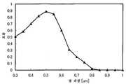
도 22는 비정질 실리콘(a-Si)과 단결정 실리콘(c-Si)의 흡수 계수들의 파장에 대한 의존도의 그래프.
도 23은 비정질 실리콘(a-Si)을 사용하는 광전 변환층의 양자 효율의 파장에 대한 의존도를 도시하는 그래프.
도 24는 단결정 실리콘(c-Si)을 사용하는 광전 변환층의 양자 효율의 파장에 대한 의존도를 도시하는 그래프.
도 25는 광전 변환층들이 적층되는 구조의 양자 효율의 파장에 대한 의존도를 도시하는 그래프.1 is a sectional view of a photoelectric conversion device;
2A and 2B are cross-sectional views of photoelectric conversion devices.
Figures 3a and 3b are cross-sectional views of photoelectric conversion devices.
4A and 4B are cross-sectional views of photoelectric conversion devices.
5A to 5E are diagrams showing a method for manufacturing a photoelectric conversion device.
6A to 6E are diagrams showing a method for manufacturing a photoelectric conversion device.
7A to 7G are diagrams showing a method for manufacturing a photoelectric conversion device.
8A to 8C show a method for processing a single crystal silicon wafer.
9A to 9C are diagrams showing a method for manufacturing a photoelectric conversion device.
10A and 10B are cross-sectional views of photoelectric conversion devices.
11 is a view showing a structure of an apparatus used for manufacturing a photoelectric conversion layer.
12 is a view showing the structure of an apparatus used for manufacturing the photoelectric conversion layer.
13A and 13B are diagrams showing a structure of a solar power generation module.
14 is a view showing a structure of a solar power generation system;
15A and 15B are diagrams showing the structure of a vehicle using a solar power generation module.
16 is a diagram showing an embodiment of an inverter.
17 is a block diagram of a switching regulator.
18 is a graph showing an output voltage from the photoelectric conversion device.
19 is a view showing an example of a photovoltaic system;
20 is a view showing a peripheral portion of the photoelectric conversion module;
21 is a view showing a peripheral portion of the photoelectric conversion module;
22 is a graph of dependence of the absorption coefficients of amorphous silicon (a-Si) and single crystal silicon (c-Si) on wavelength.
23 is a graph showing the dependence of the quantum efficiency of the photoelectric conversion layer using amorphous silicon (a-Si) on the wavelength.
24 is a graph showing the dependence of the quantum efficiency of the photoelectric conversion layer using single crystal silicon (c-Si) on the wavelength.
25 is a graph showing the dependence of the quantum efficiency of the structure in which the photoelectric conversion layers are laminated on the wavelength.
본 발명의 실시 형태들이 첨부한 도면들을 참조하여 이하에 설명될 것이다. 본 발명은 다음 설명에 제한되지 않으며, 모드들 및 상세한 부분들은 본 발명의 정신과 범주로부터 벗어남이 없이 다양한 방법들로 변화될 수 있다는 것이 당업자에 의해 쉽게 이해된다는 것을 주의한다. 따라서, 본 발명은 실시 형태들의 다음 설명에 제한되는 것으로 해석되어서는 안된다.Brief Description of the Drawings Embodiments of the present invention will be described below with reference to the accompanying drawings. It is to be noted that the present invention is not limited to the following description, and it is to be understood by those skilled in the art that modes and detailed sections can be changed in various ways without departing from the spirit and scope of the present invention. Therefore, the present invention should not be construed as being limited to the following description of the embodiments.
태양 전지 모듈 또는 태양 전지 패널을 얻기 위하여 하나 이상의 태양 전지들(전지들)이 전력을 외부로 추출하기 위한 단자에 접속된다는 것에 주의한다. 태양 전지 모듈은 전지를 습기, 먼지, 자외선들, 물리적 충격 등으로부터 전지를 보호하기 위하여 수지, 강화 유리(tempered glass), 또는 금속 프레임과 같은 보호 재료로 보강될 수 있다. 또한, 원하는 전력을 얻기 위하여 직렬로 접속되는 복수의 태양 전지 모듈들은 태양 전지 스트링(string)에 대응한다. 또한, 병렬로 배열되는 복수의 태양 전지 스트링들은 태양 전지 어레이(array)에 대응한다. 본 발명의 광전 변환 장치는 그의 카테고리에 전지, 태양 전지 모듈, 태양 전지 스트링, 그리고 태양 전지 어레이를 포함한다.Note that one or more solar cells (cells) are connected to a terminal for extracting power to the outside in order to obtain a solar cell module or a solar cell panel. The solar cell module may be reinforced with a protective material such as a resin, a tempered glass, or a metal frame to protect the battery from moisture, dust, ultraviolet rays, physical impact and the like. In addition, a plurality of solar cell modules connected in series to obtain a desired power correspond to solar cell strings. In addition, a plurality of solar cell strings arranged in parallel correspond to a solar cell array. The photoelectric conversion device of the present invention includes a battery, a solar cell module, a solar cell string, and a solar cell array in its category.
이하에 설명된 실시 형태들에서 광전 변환층은 광 조사(light irradiation)를 통해 광기전력(photoelectromotive force)을 얻기 위하여 사용되는 반도체층을 포함하는 층을 나타낸다. 즉, 광전 변환층은 p-n 접합, p-i-n 접합 등에 의해 대표된 반도체 접합 등으로 인한 광전 변환 기능을 갖는 반도체층을 나타낸다.In the embodiments described below, the photoelectric conversion layer represents a layer including a semiconductor layer used for obtaining photoelectromotive force through light irradiation. That is, the photoelectric conversion layer represents a semiconductor layer having a photoelectric conversion function due to a semiconductor junction represented by a p-n junction, a p-i-n junction, or the like.
실시 형태들의 도면들 등에서 도시된 구조들의 각각에서 층의 크기, 영역, 또는 두께는 일부 경우들에서 단순화를 위해 과장된다는 것에 주의한다. 따라서, 본 발명의 실시 형태들은 이러한 비율들에 제한되지 않는다.Note that the size, area, or thickness of a layer in each of the structures shown in the figures of the embodiments and the like is exaggerated for simplicity in some cases. Accordingly, embodiments of the present invention are not limited to these ratios.
본 명세서에서, "제 1(first)", "제 2(second)", 그리고 "제 3(third)"과 같은 서수들은 구성요소들 사이의 혼란을 피하기 위해 사용되며, 용어들이 구성요소들을 숫자적으로(numerically) 제한하지 않는다. 또한, 본 명세서의 서수들은 본 발명을 규정하는 특정 이름들을 표시하지 않는다.In this specification, ordinals such as "first," second, and "third" are used to avoid confusion among components, It is not limited numerically. In addition, the ordinal numbers in this specification do not denote specific names defining the invention.
(실시 형태 1)(Embodiment 1)
본 발명의 한 실시 형태에 따른 광전 변환 장치는 적어도 두개의 전지들을 포함한다. 전지들은 각각 광전 변환 기능을 갖는 최소 단위인 광전 변환층의 단일층 구조 또는 적층 구조를 갖는다. 또한, 광전 변환 장치는 도전성 입자(conductive particle)와 같은 도전체를 포함하는 수지를 이용하여 형성되는 적어도 하나의 구조체를 가지며, 이는 두개의 전지들 사이에 개재된다. 본 발명의 한 실시 형태에 따른 광전 변환 장치의 구조가 도 1을 참조하여 설명될 것이다.A photoelectric conversion device according to an embodiment of the present invention includes at least two cells. Each of the cells has a single layer structure or a lamination structure of the photoelectric conversion layer which is the minimum unit having a photoelectric conversion function. Further, the photoelectric conversion device has at least one structure formed by using a resin including a conductor such as a conductive particle, which is interposed between the two cells. A structure of a photoelectric conversion device according to an embodiment of the present invention will be described with reference to Fig.
도 1에 도시된 광전 변환 장치는 기판(101)(또한 제 1 기판으로 불림)에 의해 지지된 전지(102)(또한 제 1 전지로 불림), 구조체(103), 그리고 기판(104)(또한 제 2 기판으로 불림)에 의해 지지된 전지(105)(또한 제 2 전지로 불림)를 포함한다. 구조체(103)는 전지(102)와 전지(105) 사이에 개재된다. 전지(102)와 전지(105)는 각각 하나 이상의 적층되는 광전 변환층들을 갖는다. 전지(102)에 포함된 광전 변환층, 구조체(103), 그리고 전지(105)에 포함된 광전 변환층은 화살표에 의해 표시된 바와 같은 광의 진행 방향에서 서로 겹치도록 순차적으로 배열된다.1 includes a cell 102 (also referred to as a first cell) supported by a substrate 101 (also referred to as a first substrate), a
광전 변환층은 하나의 반도체 접합을 갖는다. 개시된 발명의 광전 변환 장치에서 사용될 수 있는 광전 변환층은 항상 반도체 접합을 가질 필요가 있는 것은 아니라는 것에 주의한다. 예를 들어, 광을 흡수하는 유기 염료(organic dye)를 이용하여 광기전력을 얻는 염료 감응(dye-sensitized) 광전 변환층이 또한 사용될 수 있다.The photoelectric conversion layer has one semiconductor junction. Note that the photoelectric conversion layer that can be used in the photoelectric conversion device of the disclosed invention does not always need to have a semiconductor junction. For example, a dye-sensitized photoelectric conversion layer that obtains photovoltaic power using an organic dye that absorbs light may also be used.
구조체(103)는 도전성 입자들과 같은 도전체들(106)을 포함하는 유기 수지(107)를 이용하여 형성될 수 있다. 구조체(103)는 기판(101)에 의해 지지되는 전지(102)와 기판(104)에 의해 지지된 전지(105) 사이에 개재되며, 열압착(thermocompression)되어, 전지(102), 구조체(103), 그리고 전지(105)가 서로 고정될 수 있다. 기판(101)과 기판(104)은 그 사이에 삽입된 구조체(103)와 서로 대면하도록 배열되어, 기판(101)과 기판(104)이 구조체(103)가 제공되지 않은 측면들(구조체(103)에 반대인 방향들) 상에 위치되며, 전지(102)와 전지(105)가 기판(101)과 기판(104)에 의해 보호되는 구조가 각각 형성될 수 있다는 것이 바람직하다는 것에 주의한다.The
도전체(106)는 약 수 마이크로미터에서 수십 마이크로미터의 입자 크기를 갖는 도전성 입자이며, 금, 은, 구리, 팔라듐, 백금, 몰리브덴, 크롬, 탄탈, 티타늄, 그리고 니켈 중 하나 이상의 원소들을 이용하여 형성될 수 있다. 예를 들어, 폴리스티렌과 같은 유기 수지의 표면을 원소를 사용하여 도전막으로 코팅하여 얻어진 도전성 입자가 도전체(106)로 사용될 수 있다. 또한, 도전성 입자는 투광성(light-transmitting property)을 갖는 도전성 재료, 예를 들면, 인듐 주석 산화물(ITO), 실리콘 산화물을 함유하는 인듐 주석 산화물(ITSO), 유기인듐(organoindium), 유기주석(organotin), 아연 산화물(ZnO), 아연 산화물을 함유하는 인듐 산화물(인듐 아연 산화물(IZO)), 갈륨(Ga)으로 도핑된 ZnO, 주석 산화물(SnO2), 텅스텐 산화물을 함유하는 인듐 산화물, 텅스텐 산화물을 함유하는 인듐 아연 산화물, 티타늄 산화물을 함유하는 인듐 산화물, 티타늄 산화물을 함유하는 인듐 주석 산화물 등을 사용하여 형성될 수 있다. 대안적으로, 도전성 입자의 표면이 절연막으로 덮일 수 있다. 또한, 유기 수지(107)로서, 열가소성(thermoplastic) 수지 또는 열경화성(thermosetting) 수지가 사용될 수 있다.The
도 1에서, 구조체(103)가 도전체들(106)이 유기 수지(107)에 분산되는 구조를 갖는 경우가 도시되고 있으나; 개시된 발명의 광전 변환 장치는 이러한 구성에 제한되지 않는다는 것에 주의한다. 도전체들(106)이 구조체(103)의 일부에만 존재하는 구조체(103)가 또한 채택될 수 있다.In FIG. 1, the
구조체(103)의 두께는 5㎛ 이상 100㎛ 이하, 바람직하게는, 5㎛ 이상 30㎛ 이하이다. 가요성(flexible) 기판들이 기판(101)과 기판(104)을 위하여 사용될 때, 구부러질 수 있는 얇은 광전 변환 장치가 앞서 언급된 두께를 갖는 구조체(103)를 사용하여 제작될 수 있다.The thickness of the
전지(102)와 전지(105)에 포함된 광전 변환층들 각각이 반도체 접합을 가질 때, 반도체 접합은 p-i-n 접합이거나 p-n 접합일 수 있다. 도 2a 및 도 2b의 각각에서, 전지(102)와 전지(105)가 각각 p-i-n 접합을 갖는 광전 변환 장치의 단면도가 예로서 도시된다.When each of the photoelectric conversion layers included in the
도 2a에 도시된 광전 변환 장치에서, 전지(102)(제 1 전지)는 전극으로 기능하는 도전막(110)(또한 제 1 도전막으로 불림), 광전 변환층(111)(또한 제 1 광전 변환층으로 불림), 그리고 전극으로 기능하는 도전막(112)(또한 제 2 도전막으로 불림)을 포함한다. 도전막(110), 광전 변환층(111), 그리고 도전막(112)은 기판(101) 측으로부터 순차적으로 적층된다. 광전 변환층(111)은 p 층(113)(또한 제 1 p형 반도체층으로 불림), i 층(114)(또한 제 1 i형 반도체층으로 불림), 그리고 n 층(115)(또한 제 1 n형 반도체층으로 불림)을 포함한다. p 층(113), i 층(114), 그리고 n 층(115)은 도전막(110) 측으로부터 순차적으로 적층되어, p-i-n 접합이 형성된다. 또한, 전지(105)(제 2 전지)는 전극으로 기능하는 도전막(120)(또한 제 3 도전막으로 불림), 광전 변환층(121a)(또한 제 2 광전 변환층으로 불림), 그리고 전극으로 기능하는 도전막(122)(또한 제 4 도전막으로 불림)을 포함한다. 도전막(120), 광전 변환층(121a), 그리고 도전막(122)은 기판(104) 측으로부터 순차적으로 적층된다. 광전 변환층(121a)은 p 층(125)(또한 제 2 p형 반도체층으로 불림), i 층(124)(또한 제 2 i형 반도체층으로 불림), 그리고 n 층(123)(또한 제 2 n형 반도체층으로 불림)을 포함한다. n 층(123), i 층(124), 그리고 p 층(125)은 도전막(120) 측으로부터 순차적으로 적층되어, p-i-n 접합이 형성된다.In the photoelectric conversion device shown in Fig. 2A, the battery 102 (the first battery) includes a conductive film 110 (also referred to as a first conductive film) functioning as an electrode, a
p 층은 p형 반도체층이고, i 층은 i형 반도체층이고, 또한 n 층은 n형 반도체층임에 주의한다.Note that the p-layer is a p-type semiconductor layer, the i-layer is an i-type semiconductor layer, and the n-layer is an n-type semiconductor layer.
따라서, 관심이 단지 도 2a에 도시된 광전 변환 장치의 광전 변환층(111)과 광전 변환층(121a)에 집중될 때, p 층(113), i 층(114), n 층(115), p 층(125), i 층(124), 그리고 n 층(123)이 기판(101) 측으로부터 순차적으로 적층된다. 그러므로, 구조체(103)의 도전체들(106)로 인해 p-i-n 접합들 사이에 충분한 도전성이 제공될 때, 반도체 접합들이 직렬로 접속되는 다중 접합 광전 변환 장치가 제공될 수 있다. 따라서, 제품 가격이 억제되면서 충분한 성능이 제공될 수 있다.Therefore, when the attention is focused only on the
한편, 도 2b에 도시된 광전 변환 장치에서, 광전 변환층(121b)에 포함된 p 층(125), i 층(124), 그리고 n 층(123)은 도 2a에 도시된 광전 변환층(121a)에서와 반대 순서로 적층된다.On the other hand, in the photoelectric conversion device shown in FIG. 2B, the
특히, 도 2b에 도시된 광전 변환 장치에서, 전지(102)는 전극으로 기능하는 도전막(110), 광전 변환층(111), 그리고 전극으로 기능하는 도전막(112)을 포함한다. 도전막(110), 광전 변환층(111), 그리고 도전막(112)은 기판(101) 측으로부터 순차적으로 적층된다. 광전 변환층(111)은 p 층(113), i 층(114), 그리고 n 층(115)을 포함한다. p 층(113), i 층(114), 그리고 n 층(115)은 도전막(110) 측으로부터 순차적으로 적층되어, p-i-n 접합이 형성된다. 또한, 전지(105)는 전극으로 기능하는 도전막(120), 광전 변환층(121b), 그리고 전극으로 기능하는 도전막(122)을 포함한다. 도전막(120), 광전 변환층(121b), 그리고 도전막(122)은 기판(104) 측으로부터 순차적으로 적층된다. 광전 변환층(121b)은 p 층(125), i 층(124), 그리고 n 층(123)을 포함한다. p 층(125), i 층(124), 그리고 n 층(123)은 도전막(120) 측으로부터 순차적으로 적층되어, p-i-n 접합이 형성된다.In particular, in the photoelectric conversion device shown in Fig. 2B, the
따라서, 관심이 단지 도 2b에 도시된 광전 변환 장치의 광전 변환층(111)과 광전 변환층(121b)에 집중될 때, p 층(113), i 층(114), n 층(115), n 층(123), i 층(124), 그리고 p 층(125)이 기판(101) 측으로부터 순차적으로 적층된다. 그러한 경우에, 전지(102)의 p-i-n 접합과 전지(105)의 p-i-n 접합이 전기적으로 병렬로 접속되는 방법으로 광전 변환 장치가 형성되어, 단자들의 수가 감소될 수 있다.Therefore, when the attention is focused on the
도 2b에서, p 층(113)은 n 층(115)보다 기판(101)에 더 가깝고, p 층(125)은 n 층(123)보다 기판(104)에 더 가깝지만; 개시된 발명은 이러한 구성에 제한되지 않는다는 것에 주의한다. 개시된 발명의 한 실시 형태에 따른 광전 변환 장치에서, n 층(115)은 p 층(113)보다 기판(101)에 더 가까울 수 있고, n 층(123)은 p 층(125)보다 기판(104)에 더 가까울 수 있다.2b, the p-
도 2a 및 도 2b에 도시된 광전 변환 장치들에서, 광은 기판(101) 측으로부터 들어가거나 기판(104) 측으로부터 들어갈 수 있다는 것에 주의한다. p 층(113)이 n 층(115)보다 광 입사면에 더욱 가까운 것이 바람직하다는 것에 주의한다. 캐리어로서 정공의 수명은 캐리어로서 전자의 수명의 약 절반만큼 짧다. 광이 p-i-n 접합을 갖는 광전 변환층(111)으로 들어갈 때, 대량의 전자들과 정공들이 i 층(114)에서 형성되고, 전자들은 n 층(115) 측으로 움직이며, 정공들은 p 층(113) 측으로 움직여서, 기전력이 얻어질 수 있다. 광이 p 층(113) 측으로부터 들어갈 때, 많은 전자들과 정공들이 n 층(115)보다 p 층(113)에 더 가까운 영역의 i 층(114)에서 형성된다. 따라서, 짧은 주기를 갖는 정공들이 p 층(113)으로 이동하는 거리가 짧아질 수 있으며; 결과적으로, 높은 기전력이 얻어질 수 있다. p 층(125)이 n 층(123)보다 광 입사면에 더욱 가까운 것이 바람직한 이유는 이와 동일하다.Note that, in the photoelectric conversion devices shown in Figs. 2A and 2B, light may enter from the
전지(102)와 전지(105)가 각각 도 2a와 도 2b에서 도시된 광전 변환 장치들의 각각에서 하나의 광전 변환층을 포함하는 경우가 예로서 설명되고 있으나; 개시된 발명은 이러한 구성에 제한되지 않는다. 전지(102)와 전지(105)는 각각 복수의 광전 변환층들 또는 단일 광전 변환층을 가질 수 있다. 예를 들어, 전지(102)가 복수의 광전 변환층들을 가질 때, 복수의 광전 변환층들은 기판(101) 측으로부터 순차적으로 적층된다. 광전 변환층들의 각각은 기판(101) 측으로부터 순차적으로 적층되는 p 층, i 층, 그리고 n 층을 갖는다. 광전 변환층들의 각각의 p 층, i 층, 그리고 n 층의 순서는 동일하다.Although the case where the
다음, 도 3a 및 도 3b의 각각에서, 전지(102)와 전지(105)가 각각 p-n 접합을 갖는 광전 변환 장치의 단면도가 예로써 도시된다.Next, in each of Figs. 3A and 3B, a cross-sectional view of the photoelectric conversion device in which the
도 3a에 도시된 광전 변환 장치에서, 전지(102)는 전극으로 기능하는 도전막(110), 광전 변환층(131), 그리고 전극으로 기능하는 도전막(112)을 포함한다. 도전막(110), 광전 변환층(131), 그리고 도전막(112)은 기판(101) 측으로부터 순차적으로 적층된다. 광전 변환층(131)은 p 층(133)과 n 층(135)을 포함한다. p 층(133)과 n 층(135)은 도전막(110) 측으로부터 순차적으로 적층되어, p-n 접합이 형성된다. 또한, 전지(105)는 전극으로 기능하는 도전막(120), 광전 변환층(141a), 그리고 전극으로 기능하는 도전막(122)을 포함한다. 도전막(120), 광전 변환층(141a), 그리고 도전막(122)은 기판(104) 측으로부터 순차적으로 적층된다. 광전 변환층(141a)은 p 층(143)과 n 층(145)을 포함한다. n 층(145)과 p 층(143)은 도전막(120) 측으로부터 순차적으로 적층되어, p-n 접합이 형성된다.In the photoelectric conversion device shown in Fig. 3A, the
따라서, 관심이 단지 도 3a에 도시된 광전 변환 장치의 광전 변환층(131)과 광전 변환층(141a)에 집중될 때, p 층(133), n 층(135), p 층(143), 그리고 n 층(145)이 기판(101) 측으로부터 순차적으로 적층된다. 따라서, 구조체(103)의 도전체들(106)로 인해 p-n 접합들 사이에 충분한 도전성이 제공될 때, 반도체 접합들이 직렬로 접속되는 다중 접합 광전 변환 장치가 제공될 수 있다. 따라서, 제품 가격이 억제되면서 충분한 성능이 제공될 수 있다.Therefore, when the attention is focused only on the
한편, 도 3b에 도시된 광전 변환 장치에서, 광전 변환층(141b)에 포함된 p 층(143)과 n 층(145)은 도 3a에 도시된 광전 변환층(141a)에서와 반대 순서로 적층된다.On the other hand, in the photoelectric conversion device shown in FIG. 3B, the p-
특히, 도 3b에 도시된 광전 변환 장치에서, 전지(102)는 전극으로 기능하는 도전막(110), 광전 변환층(131), 그리고 전극으로 기능하는 도전막(112)을 포함한다. 도전막(110), 광전 변환층(131), 그리고 도전막(112)은 기판(101) 측으로부터 순차적으로 적층된다. 광전 변환층(131)은 p 층(133)과 n 층(135)을 포함한다. p 층(133)과 n 층(135)은 도전막(110) 측으로부터 순차적으로 적층되어, p-n 접합이 형성된다. 또한, 전지(105)는 전극으로 기능하는 도전막(120), 광전 변환층(141b), 그리고 전극으로 기능하는 도전막(122)을 포함한다. 도전막(120), 광전 변환층(141b), 그리고 도전막(122)은 기판(104) 측으로부터 순차적으로 적층된다. 광전 변환층(141b)은 p 층(143)과 n 층(145)을 포함한다. p 층(143)과 n 층(145)은 도전막(120) 측으로부터 순차적으로 적층되어, p-n 접합이 형성된다.In particular, in the photoelectric conversion device shown in Fig. 3B, the
따라서, 관심이 단지 도 3b에 도시된 광전 변환 장치의 광전 변환층(131)과 광전 변환층(141b)에 집중될 때, p 층(133), n 층(135), n 층(145), 그리고 p 층(143)이 기판(101) 측으로부터 순차적으로 적층된다. 그러한 경우에, 전지(102)의 p-n 접합과 전지(105)의 p-n 접합이 전기적으로 병렬로 접속되는 방법으로 광전 변환 장치가 형성될 때, 단자들의 수가 감소될 수 있다.Therefore, when the attention is focused only on the
도 3b에서, p 층(133)은 n 층(135)보다 기판(101)에 더 가깝고, p 층(143)은 n 층(145)보다 기판(104)에 더 가깝지만; 개시된 발명은 이러한 구성에 제한되지 않는다는 것에 주의한다. 개시된 발명의 한 실시 형태에 따른 광전 변환 장치에서, n 층(135)은 p 층(133)보다 기판(101)에 더 가까울 수 있고, n 층(145)은 p 층(143)보다 기판(104)에 더 가까울 수 있다.3B, the p-
도 3a와 도 3b에 도시된 광전 변환 장치들에서, 광은 기판(101) 측으로부터 들어가거나 또는 기판(104) 측으로부터 들어갈 수 있다는 것에 주의한다.Note that, in the photoelectric conversion devices shown in Figs. 3A and 3B, light may enter from the
도 3a와 도 3b에 도시된 광전 변환 장치들에서, 전지(102)와 전지(105)가 각각 하나의 광전 변환층을 포함하는 경우가 예로서 설명되고 있으나; 개시된 발명은 이러한 구성에 제한되지 않는다. 전지(102)와 전지(105)는 각각 복수의 광전 변환층들 또는 단일 광전 변환층을 가질 수 있다. 예를 들어, 전지(102)가 복수의 광전 변환층들을 가질 때, 복수의 광전 변환층들은 기판(101) 측으로부터 순차적으로 적층된다. 광전 변환층들의 각각은 기판(101) 측으로부터 순차적으로 적층되는 p 층과 n 층을 갖는다. 광전 변환층들의 각각의 p 층과 n 층의 순서는 동일하다.In the photoelectric conversion devices shown in FIGS. 3A and 3B, the case where the
다음, 도 4a와 도 4b의 각각에서, 전지(102)가 복수의 p-i-n 접합들을 갖는 광전 변환 장치의 단면도가 예로써 도시된다.Next, in each of Figs. 4A and 4B, a cross-sectional view of the photoelectric conversion device in which the
도 4a에 도시된 광전 변환 장치에서, 전지(102)는 전극으로 기능하는 도전막(110), 광전 변환층(151)(또한 제 1 광전 변환층으로 불림), 광전 변환층(152)(또한 제 2 광전 변환층으로 불림), 그리고 전극으로 기능하는 도전막(112)을 포함한다. 도전막(110), 광전 변환층(151), 광전 변환층(152), 그리고 도전막(112)은 기판(101) 측으로부터 순차적으로 적층된다. 광전 변환층(151)은 p 층(153)(또한 제 1 p형 반도체층으로 불림), i 층(154)(또한 제 1 i형 반도체층으로 불림), 그리고 n 층(155)(또한 제 1 n형 반도체층으로 불림)을 포함한다. p 층(153), i 층(154), 그리고 n 층(155)은 도전막(110) 측으로부터 순차적으로 적층되어, p-i-n 접합이 형성된다. 광전 변환층(152)은 p 층(156)(또한 제 2 p형 반도체층으로 불림), i 층(157)(또한 제 2 i형 반도체층으로 불림), 그리고 n 층(158)(또한 제 2 n형 반도체층으로 불림)을 포함한다. p 층(156), i 층(157), 그리고 n 층(158)은 도전막(110) 측으로부터 순차적으로 적층되어, p-i-n 접합이 형성된다.In the photoelectric conversion device shown in Fig. 4A, the
따라서, 광전 변환층(151)과 광전 변환층(152)이 적층되는 다중 접합 전지가 도 4a에 도시된 광전 변환 장치에서 전지(102)로서 사용된다.Therefore, a multiple junction cell in which the
전지(105)는 전극으로 기능하는 도전막(120), 광전 변환층(159)(또한 제 3 광전 변환층으로 불림), 그리고 전극으로 기능하는 도전막(122)을 포함한다. 도전막(120), 광전 변환층(159), 그리고 도전막(122)은 기판(104) 측으로부터 순차적으로 적층된다. 광전 변환층(159)은 p 층(160)(또한 제 3 p형 반도체층으로 불림), i 층(161)(또한 제 3 i형 반도체층으로 불림), 그리고 n 층(162)(또한 제 3 n형 반도체층으로 불림)을 포함한다. n 층(162), i 층(161), 그리고 p 층(160)은 도전막(120) 측으로부터 순차적으로 적층되어, p-i-n 접합이 형성된다.The
도 4a에 도시된 광전 변환 장치에서, 광전 변환층(151)과 광전 변환층(152)은 직접 적층되지만; 개시된 발명은 이러한 구성에 제한되지 않는다는 것에 주의한다. 전지들이 각각 복수의 광전 변환층들을 가질 때, 도전성 중간층이 광전 변환층들 사이에 제공될 수 있다.In the photoelectric conversion device shown in Fig. 4A, the
광전 변환층(151)과 광전 변환층(152) 사이에 중간층을 갖는 광전 변환 장치의 단면도의 예가 도 4b에 도시된다. 특히, 도 4b에 도시된 광전 변환 장치에서, 전지(102)는 전극으로 기능하는 도전막(110), 광전 변환층(151), 중간층(163), 광전 변환층(152), 그리고 전극으로 기능하는 도전막(112)을 포함한다. 도전막(110), 광전 변환층(151), 중간층(163), 광전 변환층(152), 그리고 도전막(112)은 기판(101) 측으로부터 순차적으로 적층된다. 광전 변환층(151)은 p 층(153), i 층(154), 그리고 n 층(155)을 포함한다. p 층(153), i 층(154), 그리고 n 층(155)은 도전막(110) 측으로부터 순차적으로 적층되어, p-i-n 접합이 형성된다. 광전 변환층(152)은 p 층(156), i 층(157), 그리고 n 층(158)을 포함한다. p 층(156), i 층(157), 그리고 n 층(158)은 도전막(110) 측으로부터 순차적으로 적층되어, p-i-n 접합이 형성된다.An example of a cross-sectional view of a photoelectric conversion device having an intermediate layer between the
중간층(163)은 투광성을 갖는 도전막을 이용하여 형성될 수 있다. 특히, 중간층(163)은 아연 산화물, 티타늄 산화물, 마그네슘 아연 산화물, 카드뮴 아연 산화물, 카드뮴 산화물, InGaO3ZnO5와 같은 In-Ga-Zn-O계 비정질 산화물 반도체 등으로부터 형성될 수 있다. 대안적으로, 아연 산화물과 알루미늄 질화물의 혼합물을 함유하는 도전성 재료(Zn-O-Al-N계 도전성 재료로도 불리며, 각 원소의 구성요소 성분비에는 특별한 제한이 없다)가 사용될 수 있다. 중간층(163)이 도전성을 가지기 때문에, 도 4b에 도시된 광전 변환 장치에 포함된 전지(102)는 또한, 도 4a에 도시된 바와 같은 광전 변환층(151)과 광전 변환층(152)이 적층되는 다중 접합 전지에 대응한다는 것에 주의한다.The
관심이 단지 도 4a 및 도 4b에 도시된 광전 변환 장치들의 각각의 광전 변환층(151), 광전 변환층(152), 그리고 광전 변환층(159)에 집중될 때, p 층(153), i 층(154), n 층(155), p 층(156), i 층(157), n 층(158), p 층(160), i 층(161), 그리고 n 층(162)이 기판(101) 측으로부터 순차적으로 적층된다는 것에 주의한다. 그러나, 개시된 발명은 이러한 구성에 제한되지 않으며, 광전 변환층(159)에 포함된 p 층(160), i 층(161), 그리고 n 층(162)은 도 4a 및 도 4b에 도시된 광전 변환층(159)과 반대 순서로, 도 2b와 도 3b에 도시된 광전 변환 장치들과 유사한 방식으로 적층될 수 있다. 대안적으로, 광전 변환층(151)에 포함된 p 층(153), i 층(154), 그리고 n 층(155)과, 광전 변환층(152)에 포함된 p 층(156), i 층(157), 그리고 n 층(158)은 도 4a 및 도 4b에 도시된 광전 변환층들과 반대 순서로 적층될 수 있다.When the interest concentrates only on each
도 4a 및 도 4b에 도시된 광전 변환 장치들에서, 광은 기판(101) 측으로부터 들어가거나 기판(104) 측으로부터 들어갈 수 있다는 것에 주의한다. p 층(153)이 n 층(155)보다 광 입사면에 더욱 가까운 것이 바람직하다는 것에 주의한다. 캐리어로서 정공의 수명은 캐리어로서 전자의 수명의 약 절반만큼 짧다. 광이 p-i-n 접합을 갖는 광전 변환층(151)으로 들어갈 때, 대량의 전자들 및 정공들이 i 층(154)에서 형성되고, 전자들은 n 층(155) 측으로 움직이며, 정공들은 p 층(153) 측으로 움직여서, 기전력이 얻어질 수 있다. 따라서, 광이 p 층(153) 측으로부터 들어갈 때, 많은 전자들 및 정공들이 n 층(155)보다 p 층(153)에 더 가까운 영역의 i 층(154)에서 형성된다. 그러므로, 짧은 주기를 갖는 정공들이 움직이는 p 층(153)으로의 거리는 짧아질 수 있으며; 결과적으로, 높은 기전력이 얻어질 수 있다. 동일한 이유로, p 층(156)이 n 층(158)보다 광 입사면에 더욱 가까운 것이 바람직하며, p 층(160)이 n 층(162)보다 광 입사면에 더욱 가까운 것이 바람직하다.Note that, in the photoelectric conversion devices shown in Figs. 4A and 4B, light may enter from the
도 4a와 도 4b의 각각에서, 전지(102)가 두개의 광전 변환층들을 갖는 경우가 예로서 도시되고 있으나; 전지(102)는 3개 이상의 광전 변환층들을 가질 수 있다. 도 4a 및 도 4b의 각각에서, 전지(105)가 하나의 광전 변환층을 갖는 경우가 예로서 도시되고 있으나; 전지(105)는 전지(102)와 유사한 방식으로 복수의 광전 변환층들을 가질 수 있다. 예를 들어, 전지(102)가 복수의 광전 변환층들을 가질 때, 복수의 광전 변환층들은 기판(101) 측으로부터 순차적으로 적층된다. 광전 변환층들의 각각은 기판(101) 측으로부터 순차적으로 적층되는 p 층, i 층, 그리고 n 층을 갖는다. 광전 변환층들의 각각의 p 층, i 층, 그리고 n 층의 순서는 동일하다. 이러한 방식으로, 복수의 광전 변환층들이 직렬로 접속될 때, 보다 높은 기전력이 얻어질 수 있다.In each of Figs. 4A and 4B, the case where the
짧은 파장을 갖는 광은 긴 파장을 갖는 광보다 높은 에너지를 갖는다는 것에 주의한다. 따라서, 도 1, 도 2a 및 도 2b, 도 3a 및 도 3b, 그리고 도 4a 및 도 4b에 도시된 광전 변환 장치들의 각각에서 전지(102)에 포함된 광전 변환층과 전지(105)에 포함된 광전 변환층에서, 짧은 파장 범위의 광을 이용하여 광전 변환을 수행하는 광전 변환층이 광 입사면에 더 가깝고, 따라서 광전 변환 장치에서 발생하는 짧은 파장 범위의 광의 손실이 억제될 수 있으며 변환 효율이 증가될 수 있다.Note that light with shorter wavelengths has higher energy than light with longer wavelengths. Therefore, in the photoelectric conversion devices shown in Figs. 1, 2A and 2B, Figs. 3A and 3B and Figs. 4A and 4B, the photoelectric conversion layer included in the
도 1, 도 2a 및 도 2b, 도 3a 및 도 3b, 그리고 도 4a 및 도 4b에 도시된 광전 변환 장치들의 각각에서, 기판(101)과 기판(104)은 소다 석회(soda-lime) 유리, 불투명 유리, 납 유리, 강화 유리, 세라믹 유리 등의 유리 기판을 사용하여 형성될 수 있다. 또한, 알루미노실리케이트(aluminosilicate) 유리, 바륨 보로실리케이트(borosilicate) 유리, 알루미노보로실리케이트(aluminoborosilicate) 유리 등의 무알칼리(non-alkali) 유리 기판; 석영 기판; 세라믹 기판; 또는 스테인레스 스틸의 금속 기판 등이 또한 사용될 수 있다. 플라스틱과 같은 합성 수지를 이용하여 형성된 가요성 기판은 일반적으로 위의 기판들보다 내열 온도가 낮은 경향이 있지만; 이러한 기판은 제작 단계들에서 처리 온도를 견딜 수 있다면 사용될 수 있다.In each of the photoelectric conversion devices shown in Figs. 1, 2A and 2B, 3A and 3B and 4A and 4B, the
플라스틱 기판으로서, 폴리에틸렌 테레프탈레이트(polyethylene terephthalate;PET); 폴리에테르 설폰(polyether sulfone;PES); 폴리에틸렌 나프탈레이트(polyethylene naphthalate;PEN); 폴리카보네이트(polycarbonate;PC); 폴리아미드(polyamide) 합성 수지; 폴리에테르에테르케톤(polytheretherketone;PEEK); 폴리설폰(polysulfone;PSF); 폴리에테르이미드(polyetherimide;PEI); 폴리아릴레이트(polyarylate;PAR); 폴리부틸렌 테레프탈레이트(polybutylene terephthalate;PBT); 폴리이미드(polyimide); 아크릴로니트릴 부타디엔 스티렌(acrylonitrile butadiene styrene) 수지; 폴리비닐 클로라이드(polyvinyl chloride); 폴리프로필렌(polypropylene); 폴리비닐 아세테이트(polyvinyl acetate); 아크릴(acrylic) 수지; 등에 의해 대표된 폴리에스테르(polyester)를 함유하는 기판이 주어질 수 있다. 반사 방지막(anti-reflective film)이 기판의 광 입사 표면 상에 제공될 수 있다는 것에 주의한다. 예를 들어, 티타늄 산화물막 또는 구리, 망간, 니켈, 코발트, 철, 그리고 아연으로부터 선택된 적어도 하나의 금속 원소가 첨가되는 티타늄 산화물막이 반사 방지막으로 제공될 수 있다. 이러한 반사 방지막은 티타늄 산화물을 함유하는 또는 금속 원소와 티타늄 산화물을 함유하는 유기 용매가 유리 기판에 도포되고, 기판의 내열성(heat resistance)에 따라 60℃ 내지 300℃의 온도에서 베이킹(baking)이 수행되는 방식으로 형성될 수 있으며, 이로써 막의 표면은 돌출부의 최상부와 함몰부의 바닥 사이의 높이차가 10nm 내지 20nm인 요철(unevenness)을 갖게 되고; 바람직하게는, 섬모(cilia)와 같은 미세한 요철이 감소될 수 있다. 기판의 광입사 표면에 제공된 이러한 반사 방지막은 입사광의 반사와 약 2㎛ 내지 10㎛의 크기를 갖는 부유 입자들(먼지 등)의 부착이 감소되는 방식으로 작용하여, 광전 변환 장치의 변환 효율이 개선된다.As the plastic substrate, polyethylene terephthalate (PET); Polyether sulfone (PES); Polyethylene naphthalate (PEN); Polycarbonate (PC); Polyamide synthetic resin; Polyetheretherketone (PEEK); Polysulfone (PSF); Polyetherimide (PEI); Polyarylate (PAR); Polybutylene terephthalate (PBT); Polyimide; Acrylonitrile butadiene styrene resin; Polyvinyl chloride; Polypropylene; Polyvinyl acetate; Acrylic resin; And the like can be given. Note that an anti-reflective film may be provided on the light incidence surface of the substrate. For example, a titanium oxide film or a titanium oxide film to which at least one metallic element selected from copper, manganese, nickel, cobalt, iron, and zinc is added may be provided as an antireflection film. This antireflection film is formed by applying an organic solvent containing titanium oxide or an organic solvent containing a metal element and titanium oxide to a glass substrate and performing baking at a temperature of 60 to 300 DEG C depending on the heat resistance of the substrate Whereby the surface of the film has a unevenness of 10 nm to 20 nm in height difference between the top of the protrusion and the bottom of the depression; Preferably, fine irregularities such as cilia can be reduced. Such an antireflection film provided on the light incident surface of the substrate acts in such a manner that reflection of incident light and adherence of suspended particles (dust or the like) having a size of about 2 mu m to 10 mu m are reduced so that conversion efficiency of the photoelectric conversion device is improved do.
광전 변환층들에 포함된 p 층들, i 층들, 그리고 n 층들은 단결정 반도체, 다결정 반도체, 또는 미결정 반도체와 같은 결정성을 갖는 반도체를 이용하여 형성될 수 있거나, 또는 비정질 반도체를 이용하여 형성될 수 있다. 실리콘, 실리콘 게르마늄, 게르마늄, 실리콘 탄화물, 질소가 첨가된 실리콘 등이 광전 변환층들로서 사용될 수 있다.The p-layers, i-layers, and n-layers included in the photoelectric conversion layers may be formed using a semiconductor having crystallinity such as a single crystal semiconductor, a polycrystalline semiconductor, or a microcrystalline semiconductor, or may be formed using an amorphous semiconductor have. Silicon, silicon germanium, germanium, silicon carbide, silicon doped with nitrogen and the like can be used as the photoelectric conversion layers.
미결정 반도체는 비정질과 결정성 구조들(단결정 및 다결정을 포함하는) 사이의 중간 구조를 갖는 반도체라는 것에 주의한다. 미결정 반도체는 자유 에너지의 관점에서 안정한 제 3 상태를 갖는 반도체이다. 예를 들어, 미결정 반도체는 2nm 이상 200nm 이하, 바람직하게는 10nm 이상 80nm 이하, 더욱 바람직하게는 20nm 이상 50nm 이하의 결정 입자 크기를 갖는 반도체이다. 미결정 반도체의 대표적인 예인 미결정 실리콘의 라만 스펙트럼(Raman spectrum)은 단결정 실리콘의 라만 스펙트럼을 나타내는 520cm-1보다 짧은 파장측으로 시프트된다. 즉, 미결정 실리콘의 라만 스펙트럼의 피크는 단결정 실리콘을 나타내는 520cm-1부터 비정질 실리콘을 나타내는 480cm-1의 범위 내에 있다. 또한, 미결정 실리콘은 댕글링 본드(dangling bond)들을 종단시키기 위하여 적어도 1at.% 또는 그 이상의 수소 또는 할로겐을 함유한다. 더욱이, 미결정 반도체는 격자 왜곡(lattice distortion)을 더욱 촉진시키기 위하여 헬륨, 아르곤, 크립톤, 또는 네온과 같은 희가스 원소를 함유할 수 있으며, 따라서 안정성이 증가되고 양호한 미결정 반도체가 얻어질 수 있다. 이러한 미결정 반도체는 단결정 실리콘의 간접 전이(indirect transition)로부터 직접 전이(direct transition)로 광학적 특성들을 변화시키는 격자 왜곡을 갖는다. 격자 왜곡의 적어도 10%는 광학적 특성들이 직접 전이로 변화하게 만든다. 왜곡이 국부적으로 존재할 때, 직접 전이와 간접 전이가 혼합되는 광학적 특성들이 얻어질 수 있다.Note that the microcrystalline semiconductor is a semiconductor having an intermediate structure between amorphous and crystalline structures (including single crystals and polycrystals). The microcrystalline semiconductor is a semiconductor having a stable third state in view of free energy. For example, the microcrystalline semiconductor is a semiconductor having a crystal grain size of 2 nm or more and 200 nm or less, preferably 10 nm or more and 80 nm or less, and more preferably 20 nm or more and 50 nm or less. The Raman spectrum of the microcrystalline silicon, which is a typical example of the microcrystalline semiconductor, is shifted to the wavelength side shorter than 520 cm-1, which represents the Raman spectrum of the single crystal silicon. That is, the peak of the Raman spectrum of microcrystalline silicon is in the range of 480cm-1 showing the amorphous silicon from the 520cm-1 showing the single crystal silicon. In addition, the microcrystalline silicon contains at least 1 at.% Or more hydrogen or halogen to terminate the dangling bonds. Moreover, the microcrystalline semiconductor may contain a rare-gas element such as helium, argon, krypton, or neon to further promote lattice distortion, and therefore stability can be increased and a good microcrystalline semiconductor can be obtained. These microcrystalline semiconductors have lattice distortions that change optical properties from direct transition to direct transition from single crystal silicon. At least 10% of the lattice distortion causes the optical properties to change to direct transition. When distortions are localized, optical properties can be obtained in which direct and indirect transitions are mixed.
i 층을 위해 사용된 반도체는 p형 또는 n형 도전성을 부가하는 불순물 원소가 1×10²⁰/cm3이하의 농도로 함유되고, 산소와 질소가 9×10¹⁹/cm3이하의 농도로 함유되며, 광도전성(photoconductivity)이 암도전성(dark conductivity)보다 적어도 100배 높은 반도체이다. i 층은 1ppm 내지 1000ppm의 붕소를 함유할 수 있다. i 층은 때때로 가전자들(valence electrons)을 제어하기 위한 불순물 원소가 의도적으로 부가되지 않을 때 약한 n형 도전성을 갖는다. 이러한 현상은 i 층이 비정질 반도체를 이용하여 형성될 때 두드러지게 나타난다. 따라서, p-i-n 접합을 갖는 광전 변환층이 형성될 때, p형 도전성을 부가하는 불순물 원소는 성막과 동시에 또는 그 후에 i 층에 첨가될 수 있다. p형 도전성을 부가하는 불순물 원소로서, 붕소가 대표적으로 사용될 수 있으며, B2H6 또는 BF3과 같은 불순물 가스가 반도체 소스 가스로 1ppm 내지 1000ppm의 비율로 혼합될 수 있다. 붕소의 농도는 예를 들면, 1×10¹⁴/cm3 내지 6×10¹⁶/cm3일 수 있다.The semiconductor used for the i-layer has a p-type or n-type conductivity added impurity element of 1 x 10²⁰ / cm3 And oxygen and nitrogen are contained at a concentration of 9 x 10 <19 > / cm <3 & And the photoconductivity is at least 100 times higher than the dark conductivity. The i-layer may contain from 1 ppm to 1000 ppm of boron. The i-layer sometimes has a weak n-type conductivity when an impurity element for controlling valence electrons is not intentionally added. This phenomenon is conspicuous when the i-layer is formed using an amorphous semiconductor. Therefore, when a photoelectric conversion layer having a pin junction is formed, an impurity element which imparts p-type conductivity can be added to the i-layer at the same time as or after the film formation. As the impurity element to which the p-type conductivity is added, boron can be typically used, and an impurity gas such as B2 H6 or BF3 can be mixed with the semiconductor source gas at a ratio of 1 ppm to 1000 ppm. The concentration of boron may be, for example, 1 x 10¹⁴ / cm3 to 6 x 10¹⁶ / cm3 .
대안적으로, p 층이 형성된 후에 i 층이 형성될 때, p 층에 포함된 p형 도전성을 부가하는 불순물 원소가 i 층으로 확산될 수 있다. 이러한 구성으로, p형 도전성을 부가하는 불순물 원소가 i 층으로 의도적으로 첨가되지 않을 때라도, i 층의 가전자들이 제어될 수 있다.Alternatively, when the i-layer is formed after the p-layer is formed, the impurity element which adds the p-type conductivity included in the p-layer may be diffused into the i-layer. With this configuration, even when the impurity element which imparts p-type conductivity is not intentionally added to the i-layer, the valence electrons of the i-layer can be controlled.
광 입사면 상의 층은 작은 광 흡수 계수를 갖는 재료를 사용하여 형성되는 것이 바람직하다. 예를 들어, 실리콘 탄화물은 실리콘보다 작은 광 흡수 계수를 갖는다. 따라서, 실리콘 탄화물이 광입사면에 가까운 층인 p 층 또는 n 층을 위해 사용되고, 따라서 i 층에 도달하는 입사광의 양이 증가될 수 있으며; 결과적으로, 태양 전지의 기전력이 상승될 수 있다.The layer on the light incident surface is preferably formed using a material having a small light absorption coefficient. For example, silicon carbide has a smaller light absorption coefficient than silicon. Therefore, the silicon carbide is used for the p-layer or the n-layer which is a layer close to the light-incident surface, and therefore the amount of incident light reaching the i-layer can be increased; As a result, the electromotive force of the solar cell can be increased.
전지(102)와 전지(105)의 광전 변환층들에 대하여, 실리콘 또는 게르마늄과 같은 재료가 사용될 수 있으나; 개시된 발명은 이러한 구성에 제한되지 않는다는 것에 주의한다. 예를 들어, 전지(102) 또는 전지(105)로서, Cu, In, Ga, Al, Se, S 등이 광전 변환층을 위해 사용되어 CIS, CIGS로 불리는 전지, 또는 황동광(chalcopyrite) 전지가 사용될 수 있다. 대안적으로, 광전 변환층을 위하여 Cd 화합물을 사용하는 CdTe-CdS 전지가 전지(102) 또는 전지(105)를 위하여 사용될 수 있다. 염료증감 전지 또는 유기 반도체 전지와 같이, 광전 변환층을 위하여 유기계 재료를 사용하는 유기계 전지가 또한 전지(102)와 전지(105)에 사용될 수 있다.For the photoelectric conversion layers of the
광이 기판(101) 측으로부터 광전 변환 장치로 들어가면, 투광성을 갖는 투명한 도전성 재료, 특히, 인듐 산화물, 인듐 주석 산화물(ITO)의 합금, 아연 산화물 등이 기판(101)에 의해 지지된 전지(102)의 도전막(110)과 도전막(112)을 위하여 사용된다. 대안적으로, Zn-O-Al-N계 도전성 재료가 사용될 수 있다. 또한, 기판(104)에 의해 지지된 전지(105)로서, 투광성을 갖는 투명한 도전성 재료가 도전막(120)보다 광원에 가까운 도전막(122)을 위해 도전막(110)과 도전막(112)과 유사한 방식으로 사용된다. 기판(104)에 의해 지지된 전지(105)에서, 광을 쉽게 반사하는 도전성 재료, 특히, 알루미늄, 은, 티타늄, 탄탈 등이 도전막(122)보다 광원으로부터 더 먼 도전막(120)을 위해 사용된다. 위에서 설명된 것과 같은 투명한 도전성 재료는 또한 도전막(120)을 위해 사용될 수 있다는 것에 주의한다. 그러한 경우에, 전지(105)를 투과하는 광이 전지(105) 측으로 반사될 수 있는 막(반사막)이 기판(104) 상에 형성되는 것이 바람직하다. 반사막을 위하여, 알루미늄, 은, 티타늄, 또는 탄탈과 같은 쉽게 광을 반사하는 재료를 사용하는 것이 바람직하다.When a light enters the photoelectric conversion device from the side of the
광전 변환층과 접촉되는 표면 상에 요철을 형성하는 것에 의해, 쉽게 광을 반사하는 도전성 재료를 이용하여 도전막(120)이 형성되는 경우에, 광은 도전막(120)의 표면 상에서 난반사되며; 따라서, 광전 변환층의 광 흡수율이 증가될 수 있고, 변환 효율이 상승될 수 있다. 유사한 방식으로, 반사막이 형성되는 경우에, 광이 들어가는 반사막의 표면에 요철이 만들어질 때, 변환 효율이 상승될 수 있다.When the
투명한 도전성 재료로서, 인듐 산화물과 같은 금속 산화물 대신 도전성 고분자 재료(또한 도전성 폴리머로 불림)가 사용될 수 있다는 것에 주의한다. 도전성 고분자 재료로서, π-전자 공액(π-electron conjugated) 고분자가 사용될 수 있다. 예를 들어, 폴리아닐린(polyaniline) 및/또는 그의 유도체, 폴리피롤(polypyrrole) 및/또는 그의 유도체, 폴리티오펜(polythiophene) 및/또는 그의 유도체, 그리고 이러한 재료들의 둘 이상의 종류들의 공중합체가 주어질 수 있다.As a transparent conductive material, it is noted that a conductive polymer material (also referred to as a conductive polymer) may be used instead of a metal oxide such as indium oxide. As the conductive polymer material, a? -Electron conjugated polymer may be used. For example, polyaniline and / or derivatives thereof, polypyrrole and / or derivatives thereof, polythiophene and / or derivatives thereof, and copolymers of two or more of these materials may be given .
구조체(103)에 포함된 유기 수지(107)에 대해, 투광성을 갖고 전지(102)로부터 전지(105)로 광을 투과할 수 있는 재료가 사용된다. 유기 수지(107)로서, 예를 들면, 에폭시 수지, 불포화 폴리에스테르 수지, 폴리이미드 수지, 비스말레이미드-트리아진(bismaleimide-triazine) 수지, 또는 시아네이트(cyanate) 수지와 같은 열경화성 수지가 사용될 수 있다. 대안적으로, 폴리페닐린(polyphenylene) 옥사이드 수지, 폴리에테르이미드(polyetherimide) 수지, 또는 플루오린(fluorine) 수지와 같은 열가소성 수지가 유기 수지(107)로서 사용될 수 있다. 다른 대안으로서, 위에서 설명된 열경화성 수지와 열가소성 수지로부터 선택된 복수의 수지들이 유기 수지(107)로서 사용될 수 있다. 국소적 압력에 대하여 전지(102)와 전지(105)의 기계적 강도가 개선될 수 있기 때문에 유기 수지(107)의 보다 높은 유리 전이 온도가 바람직하다.A material capable of transmitting light from the
높은 열전도성의 충전재가 유기 수지(107)에 분산될 수 있다. 높은 열전도성 충전재로서, 알루미늄 질화물, 붕소 질화물, 실리콘 질화물, 알루미나 등이 주어질 수 있다. 높은 열전도성의 충전재로서, 은이나 구리와 같은 금속 입자가 또한 주어질 수 있다. 도전성 충전재가 유기 수지나 섬유들의 사속(yarn bundles)들에 포함될 때, 전지(102)와 전지(105)에서 발생된 열이 외부로 쉽게 방출될 수 있다. 따라서, 광전 변환 장치의 축열(thermal storage)이 억제될 수 있으며, 따라서 광전 변환 효율이 감소되는 것이 방지될 수 있고, 광전 변환 장치가 손상을 입는 것이 방지될 수 있다.A high thermally conductive filler can be dispersed in the
도전체(106)는 약 수 마이크로미터에서 수십 마이크로미터의 입자 크기를 갖는 도전성 입자이며, 금, 은, 구리, 팔라듐, 백금, 크롬, 니켈 중 하나 이상의 원소들을 이용하여 형성될 수 있다. 예를 들어, 폴리스티렌과 같은 유기 수지의 표면이 위의 원소를 사용하여 도전막으로 코팅되는 도전성 입자가 도전체(106)로 사용될 수 있다. 또한, 도전성 입자는 투광성을 갖는 도전성 재료, 예를 들면, 인듐 주석 산화물(ITO), 실리콘 산화물을 함유하는 인듐 주석 산화물(ITSO), 유기인듐, 유기주석, 아연 산화물(ZnO), 아연 산화물을 함유하는 인듐 산화물(인듐 아연 산화물(IZO)), 갈륨(Ga)으로 도핑된 ZnO, 주석 산화물(SnO2), 텅스텐 산화물을 함유하는 인듐 산화물, 텅스텐 산화물을 함유하는 인듐 아연 산화물, 티타늄 산화물을 함유하는 인듐 산화물, 티타늄 산화물을 함유하는 인듐 주석 산화물을 사용하여 형성될 수 있다. 대안적으로, 도전성 입자의 표면이 절연막으로 덮일 수 있다.The
개시된 발명의 한 실시 형태에 따른 광전 변환 장치에서, 도전성 입자와 같은 도전체를 포함하는 수지를 사용하여 형성된 구조체가 복수의 전지들 사이에 개재되고, 따라서 전지들로 들어가는 광이 확보되면서 복수의 전지들이 직렬로 접속될 수 있다. 따라서, 단일 전지를 사용하는 경우보다 높은 기전력을 갖는 광전 변환 장치가 형성될 수 있다. 다양한 파장들을 갖는 광을 흡수하는 복수의 전지들이 사용될 때, 자외선들로부터 적외선들까지 넓은 영역의 파장들의 광을 포함하는 태양광을 낭비없이 높은 변환 효율로 전기 에너지로 변환할 수 있는 광전 변환 장치가 보다 간단한 과정으로 형성될 수 있다.In the photoelectric conversion device according to the embodiment of the disclosed invention, a structure formed by using a resin including a conductive material such as conductive particles is interposed between a plurality of cells, so that light entering the cells is secured, May be connected in series. Therefore, a photoelectric conversion device having a higher electromotive force than when a single cell is used can be formed. When a plurality of cells that absorb light having various wavelengths are used, a photoelectric conversion device capable of converting sunlight containing light of a wide range of wavelengths from ultraviolet rays to infrared rays into electric energy with high conversion efficiency without waste It can be formed in a simpler process.
과정의 관점에서 하나의 기판 상에 연속적으로 형성되는 것이 힘든 다른 종류들의 전지들이 보다 간단한 과정으로 광의 진행 방향으로 적층될 수 있다. 따라서, 다양한 파장들을 갖는 광을 흡수하는 복수의 전지들이 서로 겹칠 수 있으며, 자외선들로부터 적외선들까지 넓은 영역의 파장들의 광을 포함하는 태양광을 낭비없이 높은 변환 효율로 전기 에너지로 변환할 수 있는, 광전 변환 장치가 보다 간단한 과정으로 형성될 수 있다. 따라서, 광전 변환 장치들을 제작하는 생산 비용이 억제될 수 있다.In view of the process, different kinds of cells, which are difficult to continuously form on one substrate, can be stacked in the proceeding direction of light in a simpler process. Accordingly, a plurality of cells that absorb light having various wavelengths can overlap with each other, and solar light including light having a wide range of wavelengths from ultraviolet rays to infrared rays can be converted into electric energy with high conversion efficiency without waste , The photoelectric conversion device can be formed in a simpler process. Therefore, the production cost for manufacturing the photoelectric conversion devices can be suppressed.
(실시 형태 2)(Embodiment 2)
본 실시 형태에서, 개시된 발명의 광전 변환 장치를 제작하기 위한 방법이 도 2a에 도시된 광전 변환 장치를 예로 사용하여 설명될 것이다.In the present embodiment, a method for manufacturing the photoelectric conversion device of the disclosed invention will be described using the photoelectric conversion device shown in Fig. 2A as an example.
먼저, 기판(101) 상의 전지(102)의 형성이 설명될 것이다. 도 5a에 도시된 바와 같이, 패터닝된(미리 정해진 모양으로 처리된) 도전막(110)이 기판(101) 상에 형성된다. 본 실시 형태에서, 광이 기판(101) 측으로부터 들어가는 광전 변환 장치가 예로서 설명되고 있으므로, 기판(101)은 가시광에 대하여 투광성을 갖는 것이 바람직하다. 예를 들어, 기판(101)은 소다-석회 유리, 불투명 유리, 납 유리, 강화 유리, 세라믹 유리 등의 다양한 상업적 유리 판들을 이용하여 형성될 수 있다. 또한, 알루미노실리케이트 유리, 바륨 보로실리케이트 유리, 알루미노보로실리케이트 유리 등의 무알칼리 유리 기판; 석영 기판; 또는 세라믹 기판이 또한 사용될 수 있다. 플라스틱들과 같은 합성 수지를 이용하여 형성된 가요성 기판(플라스틱 기판)은 일반적으로 위의 기판들보다 내열 온도가 낮은 경향이 있지만; 이러한 기판은 제작 단계들에서 처리 온도를 견딜 수 있다면 사용될 수 있다.First, the formation of the
플라스틱 기판으로서, 폴리에틸렌 테레프탈레이트(PET)로 대표되는 폴리에스테르; 폴리에테르 설폰(PES); 폴리에틸렌 나프탈레이트(PEN); 폴리카보네이트(PC); 폴리아미드 합성 섬유; 폴리에테르에테르케톤(PEEK); 폴리설폰(PSF); 폴리에테르이미드(PEI); 폴리아릴레이트(PAR); 폴리부틸렌 테레프탈레이트(PBT); 폴리이미드; 아크릴로니트릴 부타디엔 스티렌 수지; 폴리비닐 클로라이드; 폴리프로필렌; 폴리비닐 아세테이트; 아크릴 수지; 등이 주어질 수 있다.As the plastic substrate, polyester typified by polyethylene terephthalate (PET); Polyethersulfone (PES); Polyethylene naphthalate (PEN); Polycarbonate (PC); Polyamide synthetic fibers; Polyetheretherketone (PEEK); Polysulfone (PSF); Polyetherimide (PEI); Polyarylate (PAR); Polybutylene terephthalate (PBT); Polyimide; Acrylonitrile butadiene styrene resin; Polyvinyl chloride; Polypropylene; Polyvinyl acetate; Acrylic resin; Etc. can be given.
본 실시 형태에서, 광이 기판(101) 측으로부터 들어가는 광전 변환 장치가 예로서 설명되고 있기 때문에, 도전막(110)은 가시광에 대하여 투광성을 갖는 도전성 재료, 예를 들면, 인듐 주석 산화물(ITO), 실리콘 산화물을 함유하는 인듐 주석 산화물(ITSO), 유기인듐, 유기주석, 아연 산화물(ZnO), 아연 산화물을 함유하는 인듐 산화물(인듐 아연 산화물(IZO)), 갈륨(Ga)으로 도핑된 ZnO, 주석 산화물(SnO2), 텅스텐 산화물을 함유하는 인듐 산화물, 텅스텐 산화물을 함유하는 인듐 아연 산화물, 티타늄 산화물을 함유하는 인듐 산화물, 또는 티타늄 산화물을 함유하는 인듐 주석 산화물을 사용하여 형성될 수 있다. 대안적으로, 투광성을 갖는 도전성 재료로서, 도전성 고분자 재료(또한 도전성 폴리머로 불림)가 사용될 수 있다. 도전성 고분자 재료로서, π-전자 공액 고분자가 사용될 수 있다. 예를 들어, 폴리아닐린 및/또는 그의 유도체, 폴리피롤 및/또는 그의 유도체, 폴리티오펜 및/또는 그의 유도체, 그리고 이러한 재료들의 둘 이상의 종류들의 공중합체가 주어질 수 있다.In the present embodiment, since the photoelectric conversion device in which light enters from the
도전막(110)은 40nm 내지 800nm, 바람직하게는 400nm 내지 700nm의 두께를 갖도록 형성된다. 또한, 도전막(110)의 시트 저항(sheet resistance)은 약 20Ω/스퀘어 내지 200Ω/스퀘어이다.The
본 실시 형태에서, 150nm의 두께인 실리콘 산화물막과 그 표면이 주석 산화물을 사용하여 요철을 갖는 약 600nm의 두께인 도전막이 1.1mm의 두께를 갖는 소다-석회 유리의 기판(101) 상에 순차적으로 적층되는, Asahi Glass Co., Ltd.에 의해 제작된 기판(제품 이름:Asahi-U)이 사용된다. 이후, 도전막이 패터닝되어, 복수의 광전 변환층들을 전기적으로 접속하는 도전막(110)이 형성될 수 있다. 도전막(110)은 에칭, 레이저 등을 이용하여 도전막을 패터닝하는 방법에 더하여, 금속 마스크를 사용하는 증착 방법, 액적 토출(droplet discharge) 방법 등을 이용하여 형성될 수 있다는 것에 주의한다. 액적 토출 방법은 미리정해진 성분을 함유하는 액적들이 미리정해진 패턴을 형성하도록 미세한 구멍들로부터 방출되거나 분사되는 방법을 말하며, 잉크젯 방법 등을 이 카테고리에 포함한다는 것에 주의한다.In this embodiment, a silicon oxide film having a thickness of 150 nm and a conductive film having a thickness of about 600 nm having irregularities using tin oxide on the surface thereof are sequentially formed on a
광전 변환층(111) 측 상의 도전막(110)의 표면이 요철을 가질 때, 광이 굴절되거나 도전막(110) 상에서 난반사(reflected diffusely)되고; 따라서, 광전 변환층(111)의 광 흡수율이 증가될 수 있으며, 변환 효율이 상승될 수 있다.When the surface of the
다음, p 층(113), i 층(114), 그리고 n 층(115)이 순차적으로 적층되는 광전 변환층(111)이 도전막(110) 위에 형성된다. 광전 변환층(111)이 형성되기 전에, 브러쉬 세척, 또는 폴리비닐 알콜(PVA)계 다공성 재료를 사용한 세척 등이 수행되어, 도전막(110)의 표면의 청결을 개선시키기 위하여 이물질이 제거될 수 있다는 것에 주의한다. 또한, 불화수소산(hydrofluoric acid) 등을 함유하는 화학용액을 사용하여 표면이 세척될 수 있다. 본 실시 형태에서, 도전막(110)의 표면은 폴리비닐 알콜(PVA)계 다공성 재료를 사용하여 세척되며, 이후 도전막(110)의 표면이 0.5%의 불화수소 용액을 사용하여 세척된다.Next, a
p 층(113), i 층(114), 그리고 n 층(115)은 스퍼터링 방법, LPCVD 방법, 플라즈마(plasma-enhanced) CVD 방법 등을 사용하여 비정질 반도체, 다결정 반도체, 미결정 반도체 등을 이용하여 형성될 수 있다. p 층(113), i 층(114), 그리고 n 층(115)은 먼지가 그들의 계면들에 달라붙는 것을 방지하기 위하여 대기에 노출되지 않고 연속하여 형성되는 것이 바람직하다.The
대안적으로, SOI 방법을 사용하여 형성된 단결정 반도체 박막들이 p 층(113), i 층(114), 그리고 n 층(115)으로 사용될 수 있다. 단결정 반도체 박막이 사용될 때, 광전 변환층(111)은 캐리어 반송을 방해할 수 있는 결정 결함(crystal defect)들을 보다 적게 가지며; 따라서, 변환 효율이 상승될 수 있다.Alternatively, single crystal semiconductor thin films formed using the SOI method can be used as the p-
본 실시 형태에서, 실리콘 탄화물을 함유하는 비정질 반도체, 실리콘을 함유하는 비정질 반도체, 그리고 실리콘을 함유하는 미결정 반도체가 p 층(113), i 층(114), 그리고 n 층(115)으로 각각 사용된다.In this embodiment, an amorphous semiconductor containing silicon carbide, an amorphous semiconductor containing silicon, and a microcrystalline semiconductor containing silicon are used as the p-
탄소를 함유하는 가스와 실리콘을 함유하는 가스의 글로 방전 분해(glow discharge decomposition)에 의해 실리콘 탄화물을 함유하는 비정질 반도체가 얻어질 수 있다. 탄소를 함유하는 가스로서, CH4, C2H6 등이 주어질 수 있다. 실리콘을 함유하는 가스로서, SiH4, Si2H6 등이 주어질 수 있다. 실리콘을 함유하는 가스는 수소 또는 수소와 헬륨으로 희석될 수 있다. 예를 들어, 붕소가 p형 도전성을 부가하는 불순물 원소로 사용될 때, 보란(borane), 디보란(diborane), 삼불화붕소(boron trifluoride) 등이 탄소를 함유하는 가스와 실리콘을 함유하는 가스에 첨가되어, 비정질 반도체가 p형 도전성을 가질 수 있다. 특히 본 실시 형태에서, 10nm의 두께를 갖는 p 층(113)이 다음 조건들 하에서 플라즈마 CVD 방법을 사용하여 실리콘 탄화물을 갖는 p형 비정질 반도체를 사용하여 형성되는데: 메탄, 모노실란(monosilane), 수소 및 디보란의 유량들은 각각 18sccm, 6sccm, 150sccm, 그리고 40sccm이며; 반응 압력은 67Pa이고; 기판 온도는 250℃이며; 13.56MHz의 고주파수가 사용된다.An amorphous semiconductor containing silicon carbide can be obtained by glow discharge decomposition of a gas containing carbon and a gas containing silicon. As the gas containing carbon, CH4 , C2 H6 and the like can be given. As the gas containing silicon, SiH4 , Si2 H6 and the like can be given. A gas containing silicon may be diluted with hydrogen or hydrogen and helium. For example, when boron is used as an impurity element to which p-type conductivity is added, borane, diborane, boron trifluoride, or the like may be added to a gas containing carbon and a gas containing silicon So that the amorphous semiconductor can have p-type conductivity. In particular, in this embodiment, a p-
실리콘을 함유하는 비정질 반도체가 앞서 언급된 실리콘을 함유한 가스의 글로 방전 분해에 의해 얻어질 수 있다. 특히 본 실시 형태에서, 60nm의 두께를 갖는 i 층(114)이 다음 조건들 하에서 플라즈마 CVD 방법을 사용하여 실리콘을 갖는 비정질 반도체를 사용하여 형성되는데: 모노실란과 수소의 유량들은 각각 25sccm이며; 반응 압력은 40Pa이고; 기판 온도는 250℃이며; 60MHz의 고주파수가 사용된다.An amorphous semiconductor containing silicon can be obtained by the glow discharge decomposition of the above-mentioned silicon-containing gas. In particular, in this embodiment, an i-
i 층(114)이 형성되기 전에, p 층(113)의 표면 상에서 수소를 이용한 플라즈마 처리가 수행되어, p 층(113)과 i 층(114) 사이의 계면에서의 결정 결함들의 수가 감소될 수 있으며 변환 효율이 증가될 수 있다는 것에 주의한다. 특히 본 실시 형태에서, 플라즈마 처리는 다음 조건들 하에서 p 층(113)의 표면 상에서 수행되는데: 수소의 유량은 175sccm이며, 반응 압력은 67Pa이고, 기판 온도는 250℃이며, 13.56MHz의 고주파수가 사용된다. 플라즈마 처리에서, 아르곤이 수소에 부가될 수 있다. 아르곤이 부가될 때, 그의 유량은 예를 들면, 60sccm일 수 있다.Before the i-
실리콘을 함유하는 미결정 반도체가 수십 내지 수백 메가헤르츠의 주파수로 고주파수 플라즈마 CVD 또는 1Ghz 이상의 주파수로 마이크로파 플라즈마 CVD 장치에 의해 형성될 수 있다. 대표적으로, 실란 또는 디실란과 같은 실리콘 수화물, 실리콘 불화물, 또는 실리콘 염화물이 수소로 희석되어 소스 가스로 사용될 때, 미결정 반도체막이 형성될 수 있다. 또한, 실리콘 수화물, 실리콘 불화물, 또는 실리콘 염화물이 수소, 및 헬륨, 아르곤, 크립톤, 그리고 네온으로부터 하나 이상의 종류들의 선택된 희가스들과 희석될 수 있다. 실리콘 수화물과 같은 실리콘을 함유하는 화합물로의 수소의 유량비는 5:1 이상 200:1 이하, 바람직하게는 50:1 이상 150:1이하, 더욱 바람직하게는 100:1로 설정된다. 예를 들어, 인이 n형 도전성을 부가하는 불순물 원소로 이용될 때, 포스핀(phosphine) 등이 실리콘 함유 가스에 첨가될 수 있고, 따라서 미결정 반도체가 n형 도전성을 가질 수 있다. 특히 본 실시 형태에서, 10nm의 두께를 갖는 n 층(115)이 다음의 조건들 하에서 플라즈마 CVD 방법을 사용하여 실리콘을 갖는 비정질 반도체를 이용하여 형성되는데: 모노실란, 수소, 그리고 포스핀의 유량들은 각각 5sccm, 950sccm, 그리고 40sccm이며; 반응 압력은 133Pa이고; 기판 온도는 250℃이며; 13.56MHz의 고주파수가 사용된다.The microcrystalline semiconductor containing silicon can be formed by a microwave plasma CVD apparatus at a frequency of tens to hundreds of megahertz at high frequency plasma CVD or at a frequency of 1 GHz or more. Typically, when silicon hydrate such as silane or disilane, silicon fluoride, or silicon chloride is diluted with hydrogen and used as a source gas, a microcrystalline semiconductor film can be formed. In addition, silicon hydrate, silicon fluoride, or silicon chloride may be diluted with one or more selected rare gases from hydrogen, and helium, argon, krypton, and neon. The flow rate ratio of hydrogen to a compound containing silicon such as silicon hydrate is set to be 5: 1 or more and 200: 1 or less, preferably 50: 1 or more and 150: 1 or less, more preferably 100: For example, when phosphorus is used as an impurity element that adds n-type conductivity, phosphine or the like may be added to the silicon-containing gas, and thus the microcrystalline semiconductor may have n-type conductivity. Specifically, in this embodiment, an n-
인듐 주석 산화물이 도전막(110)으로 사용되는 경우에, 비정질 반도체인 p 층(113)이 도전막(110) 위에 직접 형성될 때, p 층(113)이 형성될 때 수소가 도전막(110)의 인듐 주석 산화물을 감소시키고, 이는 도전막(110)의 막 품질의 열화를 초래할 수 있다는 것에 주의한다. 인듐 주석 산화물이 도전막(110)으로 사용될 때, 인듐 주석 산화물이 감소되는 것을 방지하기 위하여, 주석 산화물을 이용하거나 아연 산화물과 알루미늄 질화물의 혼합된 재료를 함유하는 도전성 재료를 사용하여 수십 나노미터의 두께를 갖는 도전막이 인듐 주석 산화물을 이용하여 도전막 위에 적층되는 막이 도전막(110)으로 사용되는 것이 바람직하다.When indium tin oxide is used as the
광전 변환층(111)에 사용된 반도체 재료로서, 게르마늄; 갈륨 비소, 인화 인듐, 아연 셀레나이드(selenide), 갈륨 질화물과 같은 화합물 반도체; 또는 실리콘 게르마늄이 실리콘 또는 실리콘 탄화물에 부가하여 사용될 수 있다.As the semiconductor material used for the
다결정 반도체를 이용하여 광전 변환층(111)이 레이저 결정화 방법, 열 결정화 방법, 결정화를 촉진하는 니켈과 같은 촉매 원소가 사용되는 열 결정화 방법 등이 단독으로, 또는 위의 방법들의 임의의 조합으로 비정질 반도체막 또는 미결정 반도체막 상에서 결정화를 수행하여 형성될 수 있다. 대안적으로, 스퍼터링 방법, 플라즈마 CVD 방법, 열 CVD 방법 등으로 직접 다결정 반도체가 형성될 수 있다.A thermal crystallization method using a polycrystalline semiconductor, a thermal crystallization method, a thermal crystallization method, a thermal crystallization method in which a catalytic element such as nickel is used to promote crystallization, or the like may be used alone or in any combination of the above methods, Or may be formed by performing crystallization on a semiconductor film or a microcrystalline semiconductor film. Alternatively, the polycrystalline semiconductor may be directly formed by a sputtering method, a plasma CVD method, a thermal CVD method, or the like.
이후, 도 5b에 도시된 바와 같이, p 층(113), i 층(114), 그리고 n 층(115)이 순차적으로 적층되는 광전 변환층(111)이 에칭, 레이저 등을 이용하여 패터닝된다. 패터닝되고 분리되는 복수의 광전 변환층들(111)이 p 층(113) 측에서 적어도 하나의 도전막(110)과 전기적으로 접속된다.5B, the
다음, 도 5c에 도시된 바와 같이, 패터닝된 도전막(112)이 광전 변환층(111) 위에 형성된다. 본 실시 형태에서, 기판(101) 측으로부터 광이 들어가는 광전 변환 장치가 예로서 설명되기 때문에, 도전막(112)으로 가시광에 대해 투광성을 갖는 도전성 재료가 도전막(110)과 유사한 방식으로 사용되는 것이 바람직하다. 도전막(112)은 40nm 내지 800nm, 바람직하게는 400nm 내지 700nm의 두께를 갖도록 형성된다. 또한, 도전막(112)의 시트 저항은 약 20Ω/스퀘어 내지 200Ω/스퀘어일 수 있다. 본 실시 형태에서, 약 600nm의 두께를 갖는 도전막(112)이 주석 산화물을 이용하여 형성된다.Next, a patterned
패터닝되는 도전막(112)이 광전 변환층(111) 위에 도전막이 형성되고, 이후 도전막이 패터닝되는 방식으로 형성될 수 있다는 것에 주의한다. 도전막(112)은 에칭, 레이저 등을 이용하여 도전막을 패터닝하는 방법에 부가하여, 금속 마스크를 이용하는 증착 방법, 액적 토출 방법 등을 사용하여 형성될 수 있다는 것에 주의한다. 도전막(112)은 n 층(115) 측 상에서 패터닝되고 분리되는 복수의 광전 변환층들(111)의 적어도 하나와 전기적으로 접속된다. 이후, p 층(113) 측 상에서 하나의 광전 변환층(111)으로 전기적으로 접속되는 도전막(110)이, n 층(115) 측 상에서 하나의 광전 변환층(111)과 다른 광전 변환층(111)으로 전기적으로 접속되는 도전막(112)과 전기적으로 접속된다.Note that the
광전 변환층(111)과 반대인 도전막(112)의 표면은 요철을 가질 수 있다는 것에 주의한다. 이러한 구조로, 광이 굴절되거나 도전막(112) 상에서 난반사되며; 따라서, 광전 변환층(111)과 나중에 형성되는 광전 변환층(121a)의 광 흡수율이 증가될 수 있고 변환 효율이 상승될 수 있다.Note that the surface of the
다음, 기판(104) 위의 전지(105)의 형성이 설명될 것이다. 도 5d에 도시된 바와 같이, 패터닝된 도전막(120)이 기판(104) 위에 형성된다. 본 실시 형태에서, 광이 기판(101) 측으로부터 들어가는 광전 변환 장치가 예로서 설명되기 때문에, 기판(101)으로 사용될 수 있는 앞서 언급된 기판에 더하여, 절연 표면을 갖는 금속 기판과 같은 낮은 투광성을 갖는 기판이 또한 기판(104)으로 사용될 수 있다.Next, the formation of the
쉽게 광을 반사하는 도전성 재료, 특히, 알루미늄, 은, 티타늄, 탄탈 등이 도전막(120)으로 사용된다. 투광성을 갖는 앞서 언급된 도전성 재료가 또한 도전막(120)을 위하여 사용될 수 있다는 것에 주의한다. 그러한 경우에, 광이 쉽게 반사되는 재료가 기판(104)으로 바람직하게 사용되며, 또는 전지(105)를 통과하는 광이 전지(105) 측으로 반사될 수 있는 막(반사막)이 기판(104) 상에 형성되는 것이 바람직하다. 반사막은 알루미늄, 은, 티타늄, 탄탈 등을 사용하여 형성될 수 있다.A conductive material that easily reflects light, particularly aluminum, silver, titanium, tantalum, or the like, is used as the
도전막(120)이 광을 쉽게 반사시키는 도전성 재료를 사용하여 형성되는 경우에, 요철이 광전 변환층(121a)과 접촉하는 표면상에 형성될 때, 광은 도전막(120)의 표면 상에서 난반사된다. 따라서, 광전 변환층(111)과 광전 변환층(121a)의 광 흡수율이 증가될 수 있으며 변환 효율이 상승될 수 있다. 유사한 방식으로, 반사막이 형성되는 경우에, 광이 들어가는 반사막의 표면이 요철이 만들어질 때, 변환 효율이 상승될 수 있다.When the
도전막(120)은 40nm 내지 800nm, 바람직하게는 400nm 내지 700nm의 두께를 갖도록 형성된다. 또한, 도전막(120)의 시트 저항은 약 20Ω/스퀘어 내지 200Ω/스퀘어일 수 있다. 특히 본 실시 형태에서, 알루미늄을 사용한 300nm의 두께를 갖는 도전막, 은을 사용한 100nm의 두께를 갖는 도전막, 그리고 알루미늄을 함유하는 아연 산화물을 사용한 60nm의 두께를 갖는 도전막이 도전막(120)으로 사용되도록 스퍼터링 방법을 사용하여 적층된다.The
도전막이 기판(104) 위에 형성되는 방식으로, 패터닝된 도전막(120)이 형성될 수 있으며, 이후 도전막이 패터닝된다. 도전막(120)은 도전막(110)과 도전막(112)과 유사한 방식으로, 에칭, 레이저 등을 이용하여 도전막을 패터닝하는 방법에 더하여, 금속 마스크를 사용하는 증착 방법, 액적 토출 방법 등을 사용하여 형성될 수 있다는 것에 주의한다. 패터닝의 사용으로, 나중에 형성되는 복수의 광전 변환층들을 전기적으로 접속하는 도전막(120)이 형성될 수 있다.In a manner that a conductive film is formed on the
다음, n 층(123), i 층(124), 그리고 p 층(125)이 순차적으로 적층되는 광전 변환층(121a)이 도전막(120) 상에 형성된다. 광전 변환층(121a)이 형성되기 전에, 브러쉬 세척, 또는 폴리비닐 알콜(PVA)계 다공성 재료를 사용한 세척 등이 수행되어, 도전막(120)의 표면의 청결을 개선시키기 위하여 이물질이 제거될 수 있다는 것에 주의한다. 또한, 불화수소산 등을 함유하는 화학용액을 사용하여 표면이 세척될 수 있다. 본 실시 형태에서, 도전막(120)의 표면은 폴리비닐 알콜(PVA)계 다공성 재료를 사용하여 세척되며, 이후 도전막(120)의 표면이 0.5%의 불화수소 용액을 사용하여 세척된다.Next, a
n 층(123), i 층(124), 그리고 p 층(125)은 적층되는 n 층(115), i 층(114), 그리고 p 층(113)과 반대 순서로 적층되지만; n 층(123), i 층(124), 그리고 p 층(125)은 n 층(115), i 층(114), 그리고 p 층(113)과 유사한 방식으로 형성될 수 있다. 즉, n 층(123), i 층(124), 그리고 p 층(125)은 스퍼터링 방법, LPCVD 방법, 플라즈마 CVD 방법 등을 사용하여 비정질 반도체, 다결정 반도체, 미결정 반도체 등을 이용하여 형성될 수 있다. n 층(123), i 층(124), 그리고 p 층(125)은 먼지 등이 그들의 계면들에 달라붙는 것을 방지하기 위하여 대기에 노출되지 않고 연속하여 형성되는 것이 바람직하다.the n-
대안적으로, SOI 방법을 사용하여 형성된 단결정 반도체 박막들이 n 층(123), i 층(124), 그리고 p 층(125)으로 사용될 수 있다. 단결정 반도체 박막이 사용될 때, 광전 변환층(121a)은 캐리어 반송을 방해할 수 있는 결정 결함들을 보다 적게 가지며; 따라서, 변환 효율이 상승될 수 있다. 본 실시 형태에서, 실리콘 탄화물을 함유하는 비정질 반도체, 실리콘을 함유하는 비정질 반도체, 그리고 실리콘을 함유하는 미결정 반도체가 p 층(125), i 층(124), 그리고 n 층(123)으로 각각 사용된다.Alternatively, the single crystal semiconductor thin films formed using the SOI method can be used as the n-
광전 변환층(111)이 형성되는 경우에, i 층(114)이 형성되기 전에, p 층(113)의 표면 상에서 수소를 이용한 플라즈마 처리가 수행되지만; 광전 변환층(121a)이 형성되는 경우에, i 층(124)이 형성된 후에 i 층(124)의 표면 상에서 수소를 이용한 플라즈마 처리가 수행되고, 이후 p 층(125)이 형성되는 것이 바람직하다. 이러한 구조로, p 층(125)과 i 층(124) 사이의 계면에서의 결정 결함들의 수가 감소될 수 있으며, 변환 효율이 증가될 수 있다. 특히 본 실시 형태에서, 플라즈마 처리는 다음 조건들 하에서 i 층(124)의 표면 상에서 수행되는데: 수소의 유량은 175sccm이며, 반응 압력은 67Pa이고, 기판 온도는 250℃이며, 13.56MHz의 고주파수가 사용된다. 플라즈마 처리에서, 아르곤이 수소에 부가될 수 있다. 아르곤이 부가될 때, 그의 유량은 예를 들면, 60sccm일 수 있다.In the case where the
본 실시 형태에서, 광은 기판(101) 측으로부터 들어가고; 따라서, 광원에 가까운 광전 변환층(111)에 포함된 i 층(114)의 두께는 광원으로부터 먼 광전 변환층(121a)에 포함된 i 층(124)의 두께보다 작다. 본 실시 형태에서, 도전막(120) 위에, 10nm의 두께를 갖는 n 층(123), 300nm의 두께를 갖는 i 층(124), 그리고 10nm의 두께를 갖는 p 층(125)이 실리콘을 함유한 비정질 반도체, 실리콘을 함유한 비정질 반도체, 그리고 실리콘 탄화물을 함유한 p형 비정질 반도체를 각각 사용하여 순차적으로 적층된다.In this embodiment, light enters from the side of the
i 층(114)이 실리콘을 함유한 비정질 반도체를 이용하여 형성될 때, i 층(114)의 두께는 약 20nm 내지 100nm, 바람직하게는 50nm 내지 70nm라는 것에 주의한다. i 층(114)이 실리콘을 함유한 미결정 반도체를 사용하여 형성될 때, i 층(114)의 두께는 약 100nm 내지 400nm, 바람직하게는 150nm 내지 250nm이다. i 층(114)이 실리콘을 함유한 단결정 반도체를 사용하여 형성될 때, i 층(114)의 두께는 약 200nm 내지 500nm, 바람직하게는 250nm 내지 350nm이다.Note that when the i-
i 층(124)이 실리콘을 함유한 비정질 반도체를 사용하여 형성될 때, i 층(124)의 두께는 약 200nm 내지 500nm, 바람직하게는 250nm 내지 350nm이다. i 층(124)이 실리콘을 함유한 미결정 반도체를 사용하여 형성될 때, i 층(124)의 두께는 약 0.7㎛ 내지 3㎛, 바람직하게는 1㎛ 내지 2㎛이다. i 층(124)이 실리콘을 함유한 단결정 반도체를 사용하여 형성될 때, i 층(124)의 두께는 약 1㎛ 내지 100㎛, 바람직하게는 8㎛ 내지 12㎛이다.When the i-
이후, 도 5d에 도시된 바와 같이, n 층(123), i 층(124), 그리고 p 층(125)이 순차적으로 적층되는 광전 변환층(121a)이 에칭, 레이저 등을 이용하여 패터닝된다. 패터닝되고 분리되는 복수의 광전 변환층들(121a)이 n 층(123) 측 상에서 적어도 하나의 도전막(120)과 전기적으로 접속된다.5D, the
다음, 패터닝되는 도전막(122)이 광전 변환층(121a) 위에서 형성된다. 본 실시 형태에서, 광이 기판(101) 측으로부터 들어가는 광전 변환 장치가 예로서 설명되므로, 도전막(122)으로 가시광에 대한 투광성을 갖는 도전성 재료가 도전막(110)과 도전막(112)과 유사한 방식으로 사용되는 것이 바람직하다. 도전막(122)은 40nm 내지 800nm, 바람직하게는 400nm 내지 700nm의 두께를 갖도록 형성된다. 또한, 도전막(122)의 시트 저항은 약 20Ω/스퀘어 내지 200Ω/스퀘어일 수 있다. 본 실시 형태에서, 약 600nm의 두께를 갖는 도전막(122)이 주석 산화물을 이용하여 형성된다.Next, a
패터닝되는 도전막(122)이 광전 변환층(121a) 상에 도전막이 형성되는 방법으로 형성될 수 있으며, 이후 도전막이 패터닝된다는 것에 주의한다. 도전막(122)은 에칭, 레이저 등을 이용하여 도전막을 패터닝하는 방법에 더하여, 금속 마스크를 사용하는 증착 방법, 액적 토출 방법 등을 이용하여 형성될 수 있다는 것에 주의한다. 도전막(122)은 p 층(125) 측 상에서 패터닝되고 분리되는 복수의 광전 변환층들(121a) 중 적어도 하나와 전기적으로 접속된다. 이후, 하나의 광전 변환층(121a)으로 n 층(123) 측 상에서 전기적으로 접속되는 도전막(120)은, 하나의 광전 변환층(121a)과 다른 광전 변환층(121a)과 p 층(125) 측 상에서 전기적으로 접속되는 도전막(122)과 전기적으로 접속된다.Note that the
다음, 기판(101), 구조체(103), 그리고 기판(104)이 적층되어 전지(102)와 전지(105)가 전지(102)와 전지(105) 사이에 삽입된 도전성 입자들과 같은 도전체들(106)을 포함하는 유기 수지(107)를 이용하여 형성되는 구조체(103)와 서로 대면한다. 구조체(103)의 두께는 5㎛ 이상 100㎛ 이하, 바람직하게는 5㎛ 이상 30㎛ 이하이다. 기판(101)과 기판(104)이 이러한 두께를 갖는 구조체를 사용하여 가요성을 가질 때, 구부러질 수 있는 얇은 광전 변환 장치가 제작될 수 있다.Next, the
본 실시 형태에서, 도전체들(106)이 유기 수지(107)에 균일하게 분포되는 구조체(103)가 사용되지만; 개시된 발명은 이러한 구성에 제한되지 않는다는 것에 주의한다. 도전체들(106)은 단지 구조체(103)의 일부에만 존재할 수 있다.In the present embodiment, a
이후, 도 5e에 도시된 바와 같이, 구조체(103)가 가열되고 가열 및 압착되어, 구조체(103)의 유기 수지(107)가 가소화되고 경화된다. 유기 수지(107)가 유기 플라스틱 수지인 경우에, 가소화되는 유기 수지는 이후 실온으로 냉각되는 것에 의해 경화된다. 유기 수지(107)는 균일하게 분포되고 경화되어 전지(102)와 전지(105)가 가열과 압착으로 인해 서로 가깝게 부착된다. 이후, 압착으로 인해 도전체들(106)이 변형되고, 전지(102)와 전지(105)가 서로 전기적으로 접속된다. 구조체(103)가 압착되는 단계는 대기압 하에서 또는 감소된 압력 하에서 수행된다.Thereafter, as shown in Fig. 5E, the
도 2a에 도시된 광전 변환 장치가 위에서 설명된 바와 같은 제작 방법을 이용하여 형성될 수 있다.The photoelectric conversion device shown in Fig. 2A can be formed using a fabrication method as described above.
본 실시 형태에서, 미리 준비되는 구조체(103)가 전지(102)와 전지(105)에 고정되는 예가 설명되었지만; 개시된 발명은 이러한 구성에 제한되지 않는다는 것에 주의한다. 도전체들(106)이 균일하게 분포되는 유기 수지(107)가 전지(102) 또는 전지(105)에 적용되는 방법이 사용될 수 있다.In the present embodiment, an example in which the
본 실시 형태에서, 도 2a에 도시된 광전 변환 장치를 제작하는 방법이 예로서 설명되었지만; 본 발명은 이러한 구성에 제한되지 않는다. 도 2b, 도 3a 및 도 3b, 그리고 도 4a 및 도 4b에 도시된 광전 변환 장치들이 또한 본 실시 형태에서 설명된 제작 방법을 이용하여 형성될 수 있다.In this embodiment, a method of manufacturing the photoelectric conversion device shown in Fig. 2A has been described as an example; The present invention is not limited to such a configuration. The photoelectric conversion devices shown in Figs. 2B, 3A and 3B and Figs. 4A and 4B can also be formed using the fabrication method described in this embodiment.
(실시 형태 3)(Embodiment 3)
본 실시 형태에서, 광전 변환층을 포함하는 전지가 플라스틱 기판(가요성 기판) 위에 형성되고 부착되는 구성이 설명될 것이다. 특히, 다음 구조의 예가 설명될 것이다. 구조에서, 광전 변환층을 포함하는 피박리층이 그 사이에 삽입된 박리층과 절연층과 함께 유리 기판이나 세라믹 기판과 같은 높은 내열성을 갖는 지지 기판 위에 형성된 후에, 지지 기판 및 피박리층이 박리층을 이용하여 서로 분리되며, 분리되는 피박리층이 플라스틱 기판 위에 전지를 형성하기 위하여 플라스틱 기판에 부착된다. 본 실시 형태에서, 광입사면과 반대면 상에 위치되는 전지(바닥 전지)의 제작이 설명될 것이다. 본 실시 형태에서 설명된 제작 방법에 의해 형성된 전지가 광입사면 상에 위치된 전지(최상부 전지)로서 사용될 때, 광전 변환층에 포함된 전극들과 층들의 적층 순서는 적절하게 변화될 수 있다.In the present embodiment, a structure in which a cell including a photoelectric conversion layer is formed and adhered to a plastic substrate (flexible substrate) will be described. In particular, an example of the following structure will be described. In the structure, after the layer to be peeled including the photoelectric conversion layer is formed on the support substrate having high heat resistance such as a glass substrate or a ceramic substrate together with the peeling layer and the insulating layer interposed therebetween, Layer separated from each other, and a separated layer to be peeled is attached to the plastic substrate to form a battery on the plastic substrate. In this embodiment, fabrication of a battery (bottom cell) positioned on the opposite side to the light incidence plane will be described. When the cell formed by the fabrication method described in this embodiment mode is used as a cell (top cell) located on the light incidence plane, the stacking order of electrodes and layers included in the photoelectric conversion layer can be appropriately changed.
본 실시 형태의 광전 변환층은 광조사를 통해 광기전력을 생성하기 위한 반도체층들을 포함하는 층을 나타낸다. 이는 광전 변환층이 p-n 접합 또는 p-i-n 접합에 의해 대표된 반도체 접합이 형성되는 반도체층들을 나타내는 것이라고 말할 수 있다.The photoelectric conversion layer of this embodiment represents a layer including semiconductor layers for generating photovoltaic power through light irradiation. It can be said that the photoelectric conversion layer represents semiconductor layers in which a semiconductor junction represented by a p-n junction or a p-i-n junction is formed.
광전 변환층은 지지 기판 위에서 피박리층으로서 형성된다. 광전 변환층에서, 제 1 반도체층(예를 들면, p형 반도체층), 제 2 반도체층(예를 들면, i형 반도체층), 그리고 제 3 반도체층(예를 들면, n형 반도체층)이 하나의 전극(이면 전극)으로 동작하는 도전막 위에 적층된다. 대안적으로, 광전 변환층에서, 제 1 반도체층(예를 들면, p형 반도체층)과 제 3 반도체층(예를 들면 n형 반도체층)이 적층될 수 있다. 광전 변환층에 포함된 반도체층으로서, 높은 열처리없이 형성될 수 있는 비정질 실리콘, 미결정 실리콘 등을 이용한 반도체층이 사용될 수 있다. 또한, 결정성 실리콘과 같은 어느 정도의 열 또는 레이저 처리가 필요한 결정성 반도체층을 이용한 반도체층이 높은 내열성을 갖는 지지 기판을 이용하는 것에 의해 사용될 수 있다. 그러므로, 다른 분광감도 특성들을 갖는 반도체층들이 플라스틱 기판 위에 형성될 수 있기 때문에, 변환 효율이 개선될 수 있고 기판의 무게의 감소에 따라 휴대성이 개선될 수 있다.The photoelectric conversion layer is formed as a release layer on the support substrate. In the photoelectric conversion layer, a first semiconductor layer (for example, a p-type semiconductor layer), a second semiconductor layer (for example, i-type semiconductor layer), and a third semiconductor layer (for example, Is stacked on a conductive film which operates as one electrode (back electrode). Alternatively, in the photoelectric conversion layer, a first semiconductor layer (for example, a p-type semiconductor layer) and a third semiconductor layer (for example, an n-type semiconductor layer) may be laminated. As the semiconductor layer included in the photoelectric conversion layer, a semiconductor layer using amorphous silicon, microcrystalline silicon or the like which can be formed without high heat treatment can be used. Further, a semiconductor layer using a crystalline semiconductor layer which requires a certain degree of heat or a laser treatment such as crystalline silicon can be used by using a supporting substrate having high heat resistance. Therefore, since the semiconductor layers having different spectral sensitivity characteristics can be formed on the plastic substrate, the conversion efficiency can be improved and the portability can be improved as the weight of the substrate is reduced.
반도체층을 n 형 반도체층으로 변환시키기 위하여 반도체층으로 도입되는 불순물 원소의 대표적인 예로서, 주기율표의 15족에 속하는 원소들인 인, 비소, 안티몬 등이 주어진다. 또한, 반도체층을 p형 반도체층으로 변환시키기 위하여 반도체층으로 동입되는 불순물 원소의 대표적인 예로서, 주기율표의 13족에 속하는 원소들인 붕소, 알루미늄 등이 주어진다.As a representative example of the impurity element introduced into the semiconductor layer in order to convert the semiconductor layer into the n-type semiconductor layer, phosphorus, arsenic, antimony and the like belonging to group 15 of the periodic table are given. As a representative example of the impurity element which is introduced into the semiconductor layer in order to convert the semiconductor layer into the p-type semiconductor layer, boron, aluminum or the like which are elements belonging to Group 13 of the periodic table are given.
본 실시 형태에서, 제 1 반도체층, 제 2 반도체층, 그리고 제 3 반도체층이 예로서 설명되는 광전 변환층의 단면도와 동일한 번호와 동일한 모양으로 도시되었다. 그러나, 제 2 반도체층의 도전형이 p형이거나 n형인 경우에, p-n 접합이 제 1 반도체층과 제 2 반도체층 사이에서 또는 제 2 반도체층과 제 3 반도체층 사이에서 형성된다. p-n 접합의 면적은 큰 것이 바람직하며, 광에 의해 유도된 캐리어들이 재결합없이 p-n 접합으로 이동할 수 있다. 따라서, 제 1 반도체층의 수와 형상 및 제 3 반도체층의 수와 형상이 동일할 필요는 없다. 또한, 제 2 반도체층의 도전형이 i형인 경우에도, 정공의 수명이 전자보다 짧기 때문에 p-i 접합의 면적은 큰 것이 바람직하다. 따라서, 제 1 반도체층의 수와 형상 및 제 3 반도체층의 수와 형상이 p-n 접합의 경우와 같이 동일할 필요는 없다.In the present embodiment, the first semiconductor layer, the second semiconductor layer, and the third semiconductor layer are shown in the same figure and the same figure as the cross-sectional view of the photoelectric conversion layer described as an example. However, when the conductivity type of the second semiconductor layer is p-type or n-type, a p-n junction is formed between the first semiconductor layer and the second semiconductor layer or between the second semiconductor layer and the third semiconductor layer. The area of the p-n junction is preferably large, and the carriers induced by the light can move to the p-n junction without recombination. Therefore, the number and shape of the first semiconductor layers and the number and shapes of the third semiconductor layers do not have to be the same. Also, even when the conductivity type of the second semiconductor layer is i-type, since the lifetime of holes is shorter than that of electrons, it is preferable that the area of the p-i junction is large. Therefore, the number and shape of the first semiconductor layers and the number and shapes of the third semiconductor layers do not have to be the same as in the case of the p-n junction.
도 6a 내지 도 6e는 광전 변환층을 포함하는 전지의 제작 과정의 예를 도시한다.6A to 6E show an example of a manufacturing process of a cell including a photoelectric conversion layer.
먼저, 절연 표면을 갖는 지지 기판(1201) 위에, 절연층(1203), 도전막(1204), 그리고 제 1 반도체층(1205)(예를 들면, p형 반도체층), 제 2 반도체층(1206)(예를 들면, i형 반도체층), 제 3 반도체층(1207)(예를 들면, n형 반도체층)을 포함하는 광전 변환층(1221) 등이 그 사이에 박리층(1202)을 개재하여 형성된다(도 6a 참조).First, an insulating
지지 기판(1201)으로서, 높은 내열성을 갖는 기판인 유리 기판, 석영 기판, 사파이어 기판, 세라믹 기판, 절연 층이 표면 상에 제공된 금속 기판 등이 사용될 수 있다.As the supporting
박리층(1202)이 텅스텐(W), 몰리브덴(Mo), 티타늄(Ti), 탄탈(Ta), 니오브(Nb), 니켈(Ni), 코발트(Co), 지르코늄(Zr), 아연(Zn), 루테늄(Ru), 로듐(Rh), 팔라듐(Pd), 오스뮴(Os), 이리듐(Ir), 그리고 실리콘(Si)으로부터 선택된 원소, 또는 이러한 원소를 함유하는 합금 재료나 화합물 재료를 그의 주요 구성성분으로 사용하여, 스퍼터링 방법, 플라즈마 CVD 방법, 코팅 방법, 프린팅 방법 등에 의해 단일층 또는 적층된 층들로 형성된다. 실리콘을 함유하는 층의 결정 구조는 비정질, 미결정, 또는 다결정일 수 있다. 여기서 코팅 방법은 스핀 코팅 방법, 액적 토출 방법, 디스펜싱(dispensing) 방법, 노즐 프린팅 방법, 그리고 슬롯 다이 코팅(slot die coating) 방법을 포함한다는 것에 주의한다.The
박리층(1202)이 단일층 구조를 가질 때, 텅스텐 층, 몰리브덴 층, 또는 텅스텐과 몰리브덴의 혼합물을 함유하는 층을 형성하는 것이 바람직하다. 대안적으로, 텅스텐의 산화물 또는 산화질화물을 함유하는 층, 몰리브덴의 산화물 또는 산화질화물을 함유하는 층, 또는 텅스텐과 몰리브덴의 혼합물의 산화물 또는 산화질화물을 함유하는 층이 형성된다. 예를 들어, 텅스텐과 몰리브덴의 혼합물은 텅스텐과 몰리브덴의 합금에 대응한다는 것을 주의한다.When the
박리층(1202)이 적층 구조를 가질 때, 제 1 층으로서, 텅스텐 층, 몰리브덴 층, 또는 텅스텐과 몰리브덴의 혼합물을 함유하는 층을 형성하고, 제 2 층으로서, 텅스텐, 몰리브덴 또는 텅스텐과 몰리브덴의 혼합물의 산화물, 질화물, 산화질화물 또는 질화산화물의 층을 형성하는 것이 바람직하다.When the
텅스텐을 함유하는 층과 그 위에 산화물을 이용하여 형성된 절연층의 형성에 의해 박리층(1202)이 텅스텐을 함유하는 층과 텅스텐의 산화물을 함유하는 층의 적층 구조로 형성될 때, 텅스텐의 산화물을 함유하는 층은 텅스텐층과 절연층 사이의 계면에 형성된다. 대안적으로, 텅스텐을 함유하는 층의 표면이 열 산화 처리, 산소 플라즈마 처리, 오존 수액과 같은 강 산화 용액을 이용한 처리 등을 겪어 텅스텐의 산화물을 함유하는 층이 형성될 수 있다. 플라즈마 처리 또는 열 처리가 산소 또는 일산화 이질소와 같은 가스; 또는 가스와 다른 가스의 혼합된 가스의 분위기에서 형성될 수 있다. 동일한 처리가 텅스텐의 질화물, 산화질화물, 또는 질화산화물을 함유하는 층을 형성하는 경우에 적용될 수 있다. 텅스텐을 함유하는 층이 형성된 후에, 실리콘 질화물층, 실리콘 산화질화물층, 또는 실리콘 질화산화물층이 그 위에 형성될 수 있다.When the
베이스로 동작하는 절연층(1203)이 실리콘 산화물막, 실리콘 질화물막, 실리콘 산화질화물막, 또는 실리콘 질화산화물막과 같은 무기 절연막을 이용하는 것에 의해 단일층 또는 복수의 층들로 형성될 수 있다.The insulating
본 명세서에서, 실리콘 산화질화물은 질소의 양보다 많은 산소의 양을 함유하는 물질을 나타낸다. 예를 들어, 실리콘 산화질화물은 산소, 질소, 실리콘, 그리고 수소를 각각 50at.% 내지 70at.%, 0.5at.% 내지 15at.%, 25at.% 내지 35at.%, 그리고 0.1at.% 내지 10at.%의 농도 범위로 함유한다. 또한, 실리콘 질화산화물은 산소의 양보다 많은 질소의 양을 함유하는 물질을 나타낸다. 예를 들어, 실리콘 질화산화물은 산소, 질소, 실리콘, 그리고 수소를 각각 5at.% 내지 30at.%, 20at.% 내지 55at.%, 25at.% 내지 35at.%, 그리고 10at.% 내지 25at.%의 농도 범위로 함유한다. RBS(Rutherford backscattering spectrometry) 또는 HFS(hydrogen forward scattering spectrometry)를 이용하여 측정이 수행되는 경우에 산소, 질소, 실리콘, 그리고 수소의 함량들이 앞서 언급된 범위들에 속한다는 것에 주의한다. 또한, 구성 원소들의 총 함량들은 100 at.%를 넘지 않는다.In this specification, silicon oxynitride refers to a material containing an amount of oxygen greater than the amount of nitrogen. For example, the silicon oxynitride may include oxygen, nitrogen, silicon, and hydrogen in an amount ranging from 50 at.% To 70 at.%, 0.5 at. To 15 at.%, 25 at. %. ≪ / RTI > Also, silicon nitride oxide represents a material containing an amount of nitrogen greater than the amount of oxygen. For example, the silicon nitride oxide may include oxygen, nitrogen, silicon, and hydrogen in amounts of about 5 at.% To about 30 at.%, About 20 at.% To about 55 at.%, About 25 at. By weight. It should be noted that the contents of oxygen, nitrogen, silicon, and hydrogen fall within the ranges mentioned above when measurements are performed using RBS (Rutherford backscattering spectrometry) or HFS (hydrogen forward scattering spectrometry). In addition, the total content of constituents does not exceed 100 at.%.
알루미늄, 은, 티타늄, 또는 탄탈과 같은 높은 반사율을 갖는 금속막을 이용하여 도전막(1204)을 형성하는 것이 바람직하다. 증착 방법 또는 스퍼터링 방법이 도전막(1204)을 형성하는데 사용될 수 있다는 것에 주의한다. 또한, 도전막(1204)은 복수의 층들을 이용하여 형성될 수 있다. 예를 들어, 도전막(1204)과 제 1 반도체층(1205) 사이의 접착을 개선시키기 위한 버퍼층 등이 금속막, 금속 산화물막, 금속 질화물막 등을 이용하여 형성되고 적층될 수 있다. 또한, 도전막(1204)의 표면이 텍스처 구조(texture structure)(요철 구조)를 갖기 위하여 에칭 처리 등에 의해 처리될 수 있다. 도전막(1204)의 표면이 텍스처 구조를 가질 때, 광이 난반사되어, 입사광이 효율적으로 전기 에너지로 변환될 수 있다. 텍스처 구조는 입사광의 반사를 방지하고 광전 변환층으로 들어가는 광량이 광을 난반사하는 것에 의해 증가될 수 있어 변환 효율이 개선될 수 있는 요철 구조를 말한다는 것에 주의한다.It is preferable to form the
제 1 반도체층(1205), 제 2 반도체층(1206), 그리고 제 3 반도체층(1207)이 다음 재료들: 실란 또는 게르만에 의해 대표되는 반도체 소스 가스를 이용하는 기상 성장 방법 또는 스퍼터링 방법에 의해 형성된 비정질 반도체; 광 에너지 또는 열 에너지를 이용하여 비정질 반도체를 결정화하는 것에 의해 형성된 다결정 반도체; 미결정(또한 세미-아모퍼스 또는 마이크로크리스탈로도 불림) 반도체 등 중 임의의 것을 이용하여 형성될 수 있다. 반도체층은 스퍼터링 방법, LPCVD 방법, 플라즈마 CVD 방법 등에 의해 형성될 수 있다.The
깁스(Gibbs) 자유 에너지가 고려될 때, 미결정 반도체막은 비정질 구조와 단결정 구조 사이의 중간 구조의 준안정(metastable) 상태를 갖는다. 즉, 미결정 반도체막은 자유 에너지의 관점에서 안정하고, 단범위 질서(short-range order)와 격자 왜곡을 갖는 제 3 상태를 갖는 반도체를 포함한다. 원주형 또는 바늘형 결정들이 기판 표면에 대하여 수직 방향으로 성장한다. 미결정 반도체의 대표적인 예인 미결정 실리콘의 라만 스펙트럼은 단결정 실리콘을 나타내는 520cm-1보다 작은 파수(wavenumber)로 시프트된다. 즉, 미결정 실리콘의 라만 스펙트럼의 피크는 단결정 실리콘을 나타내는 520cm-1과 비정질 실리콘을 나타내는 480cm-1사이에 존재한다. 또한, 미결정 실리콘은 댕글링 본드들을 종결시키기 위하여 적어도 1at.%의 수소 또는 할로겐을 함유한다. 더욱이, 미결정 실리콘은 격자 왜곡을 더욱 촉진하기 위하여 헬륨, 아르곤, 크립톤, 또는 네온과 같은 희가스 원소를 함유하며, 따라서 안정성이 증가되고 양호한 미결정 반도체막이 얻어질 수 있다.When Gibbs free energy is taken into consideration, the microcrystalline semiconductor film has a metastable state of an intermediate structure between an amorphous structure and a single crystal structure. That is, the microcrystalline semiconductor film is stable in terms of free energy, and includes a semiconductor having a third state with short-range order and lattice distortion. Columnar or needle-like crystals grow in a direction perpendicular to the substrate surface. Raman spectrum of microcrystalline silicon typical examples of a microcrystalline semiconductor is shifted to the small wave number (wavenumber) than 520cm-1 showing the single crystal silicon. That is, the peak of the Raman spectrum of microcrystalline silicon is 480cm to 520cm-1 showing an amorphous silicon indicates a single crystallinesilicon-existing betweenthe. In addition, the microcrystalline silicon contains at least 1 at.% Hydrogen or halogen to terminate the dangling bonds. Moreover, the microcrystalline silicon contains a rare-gas element such as helium, argon, krypton, or neon to further promote lattice distortion, and therefore stability can be improved and a good microcrystalline semiconductor film can be obtained.
비정질 반도체의 대표적인 예들은 수소화된 비정질 실리콘을 포함하지만, 결정화 반도체의 대표적인 예들은 폴리실리콘을 포함한다. 폴리실리콘(다결정 실리콘)의 예들은, 주요 구성요소로서 폴리실리콘을 함유하며 800℃ 이상의 처리 온도에서 형성되는 소위 고온 폴리실리콘과, 주요 구성요소로서 폴리실리콘을 함유하며 600℃ 이하의 처리 온도에서 형성되는 소위 저온 폴리실리콘과, 결정화를 촉진하는 원소를 사용하는 것에 의해 비정질 실리콘을 결정화하여 얻어진 폴리실리콘 등을 포함한다. 미결정 반도체 또는 결정 상을 부분적으로 포함하는 반도체가 또한 위에서 설명된 것으로 사용될 수 있다는 것은 말할 필요가 없다.Representative examples of amorphous semiconductors include hydrogenated amorphous silicon, but representative examples of crystallization semiconductors include polysilicon. Examples of polysilicon (polycrystalline silicon) include so-called high temperature polysilicon containing polysilicon as a main component and formed at a processing temperature of 800 DEG C or higher, polysilicon as a main component and formed at a processing temperature of 600 DEG C or lower And polysilicon obtained by crystallizing amorphous silicon by using an element for promoting crystallization and the like. It is needless to say that semiconducting semiconductors or semiconductors partially containing crystal phases can also be used as described above.
또한, 제 1 반도체층(1205), 제 2 반도체층(1206), 그리고 제 3 반도체층(1207)이 또한 실리콘과 실리콘 탄화물에 더하여, 게르마늄 또는 갈륨 비소, 인듐 인화물, 아연 셀레나이드, 갈륨 질화물, 또는 실리콘 게르마늄과 같은 화합물 반도체를 이용하여 형성될 수 있다.The
반도체층으로 결정성 반도체층을 사용하는 경우에, 결정성 반도체층은 레이저 결정화 방법과 열 결정화 방법과 같은 임의의 다양한 방법들에 의해서 형성될 수 있다. 비정질 반도체층이 열 처리와 레이저 광 조사의 조합을 이용하여 결정화될 수 있다. 열 처리 또는 레이저 광 조사는 개별적으로 수 번에 걸쳐 수행될 수 있다.In the case of using the crystalline semiconductor layer as the semiconductor layer, the crystalline semiconductor layer may be formed by any of various methods such as a laser crystallization method and a thermal crystallization method. The amorphous semiconductor layer can be crystallized using a combination of heat treatment and laser light irradiation. The heat treatment or laser light irradiation can be carried out individually several times.
플라즈마 CVD 방법에 의해 결정성 반도체층이 직접 기판 위에 형성될 수 있다. 대안적으로, 플라즈마 CVD 방법에 의해 결정성 반도체층이 기판 위에 선택적으로 형성될 수 있다. 결정들이 원주 모양으로 성장하는 원주 구조를 갖도록 결정성 반도체층이 지지 기판(1201) 위에 형성되는 것이 바람직하다는 것에 주의한다.The crystalline semiconductor layer can be directly formed on the substrate by the plasma CVD method. Alternatively, the crystalline semiconductor layer can be selectively formed on the substrate by the plasma CVD method. Note that it is preferable that the crystalline semiconductor layer is formed on the supporting
제 1 도전형(예를 들면, p형 도전성)을 부가하는 불순물 원소가 제 1 반도체층(1205)과 제 3 반도체층(1207) 중 하나로 도입되고, 제 2 도전형(예를 들면, n형 도전성)을 부가하는 불순물 원소가 다른 것으로 도입된다는 것에 주의한다. 또한, 바람직하게는, 제 2 반도체층(1206)은 진성 반도체층이거나 또는 제 1 또는 제 2 도전형을 부가하는 불순물 원소가 도입되는 층이다. 본 실시 형태에서 광전 변환층으로서 p-i-n 접합을 형성하도록 3개의 반도체층들이 적층되는 예가 설명되었으나; 다수의 반도체층들이 p-n 접합과 같은 다른 접합을 형성하기 위해 또한 적층될 수 있다.An impurity element which adds a first conductivity type (for example, a p-type conductivity) is introduced into one of the
앞에서 말한 과정을 통하여, 박리층(1202)과 절연층(1203) 위에, 도전막(1204)과 제 1 반도체층(1205), 제 2 반도체층(1206), 제 3 반도체층(1207)을 포함하는 광전변환층(1221) 등이 형성될 수 있다.The
이후, 절연층(1203) 위에 도전막(1204), 제 1 반도체층(1205), 제 2 반도체층(1206), 그리고 제 3 반도체층(1207)을 포함하는 피박리층이 박리를 위한 접착제(1209)를 사용하여 임시 지지 기판(1208)에 부착되고, 피박리층이 박리층(1202)을 사용하여 지지기판(1201)으로부터 분리된다. 이러한 과정에 의해, 피박리층이 임시 지지 기판(1208) 측 상에 위치된다(도 6b 참조).Thereafter, a layer to be peeled including the
임시 지지 기판(1208)으로서, 유리 기판, 석영 기판, 사파이어 기판, 세라믹 기판, 금속 기판 등이 사용될 수 있다. 또한, 본 실시 형태의 처리 온도를 견디기 위한 내열성을 갖는 플라스틱 기판 또는 필름과 같은 가요성 기판이 또한 사용될 수 있다.As the
또한, 여기서 사용되는 박리를 위한 접착제(1209)로서, 물이나 용액에 녹을 수 있는 접착제, UV 광 등을 조사할 때 가소화될 수 있는 접착제가 사용되어 임시 지지 기판(1208)과 피박리층이 필요할 때 화학으로 또는 물리적으로 서로 분리될 수 있다.As an adhesive 1209 for peeling, an adhesive capable of being plasticized when irradiating an adhesive capable of dissolving in water or a solution, UV light, or the like is used, so that the
예로써 설명되는, 피박리층을 임시 지지 기판으로 반송하는 위의 과정은 또한 다른 방법에 의해 수행될 수 있다. 예를 들어, 다음 방법들: 박리층이 기판과 피박리층 사이에 형성되고, 금속 산화물막이 박리층과 피박리층 사이에 제공되며, 피박리층의 박리를 수행하도록 금속 산화물막이 결정화에 의해 약화되는 방법; 수소를 함유하는 비정질 실리콘막이 높은 내열성의 지지 기판과 피박리층 사이에 제공되고, 피박리층의 박리를 수행하도록 레이저 광 조사나 에칭에 의해 비정질 실리콘막이 제거되는 방법; 박리 층이 지지 기판과 피박리층 사이에 형성되고, 금속 산화물막이 박리층과 피박리층 사이에 제공되며, 금속 산화물막이 결정화에 의해 약화되며, 약화된 금속 산화물막에서 박리를 수행하도록 용액 또는 NF3, BrF3, 또는 ClF3과 같은 불화 할로겐 가스를 사용하여 박리층의 일부가 에칭되어 제거되는 방법; 피박리층이 제공된 지지 기판이 기계적으로 제거되거나 용액 또는 NF3, BrF3, 또는 ClF3과 같은 불화 할로겐 가스를 사용하여 에칭되어 제거되는 방법; 등 중 임의의 것이 적절하게 사용될 수 있다. 또한, 질소, 산소, 수소 등을 함유하는 막(예를 들면, 수소를 함유하는 비정질 실리콘막, 수소를 함유하는 합금막, 또는 산소를 함유하는 합금막)이 박리층으로 사용되고, 레이저 광으로 조사되어, 피박리층과 기판 사이의 박리를 촉진하도록 박리층에 함유된 질소, 산소, 또는 수소가 가스로 방출되는 방법을 사용하는 것이 또한 가능하다.The above process of transporting the layer to be peeled to the temporary support substrate, which is described by way of example, may also be performed by other methods. For example, the following methods: a method in which a release layer is formed between a substrate and a layer to be peeled, a metal oxide film is provided between the release layer and the layer to be peeled, and the metal oxide film is weakened by crystallization How to do it; A method in which an amorphous silicon film containing hydrogen is provided between a support substrate having a high heat resistance and a layer to be peeled and the amorphous silicon film is removed by laser light irradiation or etching so as to perform peeling of the layer to be peeled; A release layer is formed between the support substrate and the layer to be peeled, a metal oxide film is provided between the release layer and the release layer, the metal oxide film is weakened by crystallization, and a solution or NF3 , BrF3 , or ClF3 to remove a part of the release layer by etching; A method in which the support substrate provided with the layer to be peeled is mechanically removed or etched away using a solution or halogen fluoride gas such as NF3 , BrF3 , or ClF3 ; And the like can be appropriately used. Further, a film containing nitrogen, oxygen, hydrogen or the like (for example, an amorphous silicon film containing hydrogen, an alloy film containing hydrogen, or an alloy film containing oxygen) is used as the peeling layer, It is also possible to use a method in which the nitrogen, oxygen, or hydrogen contained in the release layer is released into the gas so as to promote the separation between the layer to be peeled and the substrate.
복수의 위에서 설명된 박리 방법들이 조합될 때, 반송 과정이 쉽게 수행될 수 있다. 즉, 분리는 레이저 광 조사의 수행; 가스, 액체 등으로 박리층 상에서의 에칭; 또는 날카로운 칼, 메스(scalpel), 등으로의 기계적 제거 후에 박리층과 피박리층이 서로 쉽게 박리될 수 있는 상황을 만들도록 물리적 힘(기계 등에 의한)으로 수행될 수 있다.When a plurality of the peeling methods described above are combined, the conveying process can be easily performed. That is, separation is performed by performing laser light irradiation; Etching on the delamination layer by gas, liquid or the like; Or by mechanical force (such as by a machine) to create a situation in which the release layer and the release layer can easily peel off from each other after mechanical removal with a sharp knife, scalpel, and the like.
또한, 액체가 박리층과 피박리층 사이의 계면에 침투시킨 후에, 또는 물이나 에탄올과 같은 액체가 이 계면 상에 흐르는 동안, 피박리층이 지지 기판으로부터 또한 박리될 수 있다.Further, the layer to be peeled can also be peeled off from the support substrate after the liquid penetrates the interface between the peeling layer and the layer to be peeled, or while the liquid such as water or ethanol is flowing on this interface.
더욱이, 박리층(1202)이 텅스텐을 사용하여 형성될 때는, 암모늄 수액과 과산화수소 용액의 혼합 용액을 이용하여 박리층을 에칭시키는 동안 분리가 수행되는것이 바람직하다.Furthermore, when the
다음, 지지 기판(1201)으로부터 박리되고 박리층(1202) 또는 절연층(1203)이 노출되는 피박리층이 접착층(1210)을 이용하여 플라스틱 기판(1211)에 부착된다(도 6c 참조).Next, a layer to be peeled off from the
부착층(1210)을 위한 재료로서, 반응 경화형 접착제, 열 경화형 접착제, 자외선 경화형 접착제와 같은 광 경화형 접착제와 같은 다양한 경화형 접착제들 및 혐기성 접착제 중 임의의 것이 사용될 수 있다.As the material for the
플라스틱 기판(1211)으로서, 가요성과 가시광에 대하여 투과성을 갖는 다양한 기판들 중 임의의 것이 사용될 수 있으며, 유기 수지 등의 막이 사용되는 것이 바람직하다. 예를 들어, 유기 수지로서, 아크릴 수지, 폴리에틸렌 테레프탈레이트(PET) 또는 폴리에틸렌 나프탈레이트(PEN)와 같은 폴리에스테르 수지, 폴리아크릴로니트릴 수지, 폴리이미드 수지, 폴리메틸 메타크릴레이트 수지, 폴리카보네이트(PC) 수지, 폴리에테르설폰(PES) 수지, 폴리아미드 수지, 사이클로올레핀 수지, 폴리스티렌 수지, 폴리아미드 이미드 수지, 폴리비닐클로라이드 수지 등이 사용될 수 있다.As the
플라스틱 기판(1211) 위에, 질소와 실리콘, 예를 들면 실리콘 질화물 또는 실리콘 산화질화물을 함유한 막 또는 알루미늄 질화물과 같은 질소와 알루미늄을 함유하는 막과 같은 낮은 투수성을 갖는 보호층이 미리 형성될 수 있다.On the
그 후에, 박리용 접착제(1209)를 용해 또는 가소화시키는 것에 의해 임시 지지 기판(1208)이 제거된다(도 6d 참조). 이후, 광전 변환층(1221)을 원하는 모양 등으로 처리하는 과정을 수행한 후에, 다른 전극(표면 전극)으로 동작하는 도전막(1212)이 제 3 반도체층(1207) 위에 형성된다(도 6e 참조).Thereafter, the temporary supporting
앞의 방법으로, 광전 변환층을 포함하는 전지가 플라스틱 기판과 같은 기판으로 반송될 수 있다. 본 실시 형태에서 광전 변환층을 포함하는 전지는 위의 실시 형태에서 설명된 바와 같은 도전성 수지를 이용하여 다른 광전 변환층을 포함하는 전지에 결합될 수 있으며, 따라서 광전 변환 장치가 제작될 수 있다.In the foregoing method, the battery including the photoelectric conversion layer can be transported to a substrate such as a plastic substrate. In the present embodiment, a battery including a photoelectric conversion layer can be coupled to a battery including another photoelectric conversion layer using a conductive resin as described in the above embodiments, and thus a photoelectric conversion device can be manufactured.
도전막(1212)은 광스퍼터링 방법 또는 진공 증착 방법에 의해 형성될 수 있다는 것에 주의한다. 도전막(1212)은 광을 충분히 전달하는 재료를 이용하여 형성되는 것이 바람직하다. 위의 재료의 예들은 인듐 주석 산화물(ITO), 실리콘 산화물을 함유하는 인듐 주석 산화물(ITSO), 유기인듐, 유기주석, 아연 산화물(ZnO), 아연 산화물을 함유하는 인듐 산화물(인듐 아연 산화물(IZO)), 갈륨(Ga)으로 도핑된 ZnO, 주석 산화물(SnO2), 텅스텐 산화물을 함유하는 인듐 산화물, 텅스텐 산화물을 함유하는 인듐 아연 산화물, 티타늄 산화물을 함유하는 인듐 산화물, 그리고 티타늄 산화물을 함유하는 인듐 주석 산화물을 포함한다. 또한, 투광성을 갖는 도전성 재료로서, 도전성 고분자 재료(또한 도전성 폴리머로 불림)가 사용될 수 있다. 도전성 고분자 재료로서, π 전자 공액 도전성 폴리머가 사용될 수 있다. 예를 들어, 폴리아닐린 및/또는 그의 유도체, 폴리피롤 및/또는 그의 유도체, 폴리티오펜 및/또는 그의 유도체, 그리고 이러한 재료들의 둘 이상의 종류들의 공중합체 등이 주어질 수 있다.Note that the
본 실시 형태는 임의의 다른 실시 형태들과 적절하게 조합될 수 있다는 것에 주의한다.It should be noted that this embodiment may be combined with any other embodiment as appropriate.
(실시 형태 4)(Fourth Embodiment)
본 실시 형태는 단결정 반도체 기판을 유리, 세라믹 등으로 만들어진 지지 기판에 결합시키는 것에 의해 광전 변환층을 포함하는 전지를 형성하기 위한 방법에 관한 것이며, 그의 한 예가 설명될 것이다. 본 실시 형태에서, 광 입사면에 반대인 면에 위치되는 전지(바닥 전지)의 제작이 설명될 것이다. 본 실시 형태에서 설명된 제작 방법에 의해 형성된 전지가 광 입사면 상에 위치된 전지(최상부 전지)로 사용될 때, 광전 변환층에 포함된 전극들과 층들의 적층 순서는 적절하게 변화될 수 있다.This embodiment relates to a method for forming a cell including a photoelectric conversion layer by bonding a single crystal semiconductor substrate to a support substrate made of glass, ceramics or the like, and an example thereof will be described. In this embodiment, fabrication of a battery (bottom cell) positioned on the surface opposite to the light incidence surface will be described. When the cell formed by the fabrication method described in this embodiment mode is used as a cell (top cell) located on the light incident surface, the stacking order of the electrodes and layers included in the photoelectric conversion layer can be appropriately changed.
지지 기판에 결합될 단결정 반도체 기판에 취화(fragile)층이 형성된다. 단결정 반도체 기판 위에, 하나의 전극(이면 전극)으로 동작하는 도전막, 제 1 반도체층, 제 2 반도체층, 그리고 제 3 반도체층이 적층되는 광전 변환층, 그리고 지지 기판에 결합될 절연층이 미리 형성된다. 이후, 지지 기판 및 절연층이 서로 가까이 부착되고, 이후, 취화층 주위로 박리가 수행되어, 단결정 반도체층이 광전 변환층에서의 반도체층들로 이용되는 광전 변환 장치가 지지 기판 위에 제작될 수 있다. 따라서, 캐리어 반송을 방해할 수 있는 결정 결함들을 보다 적게 갖는 광전 변환층을 포함하는 전지가 제작될 수 있으며, 광전 변환 장치가 우수한 변환 효율을 가질 수 있다.A fragile layer is formed on the single crystal semiconductor substrate to be bonded to the supporting substrate. A photoelectric conversion layer in which a conductive film that operates as one electrode (back electrode), a first semiconductor layer, a second semiconductor layer, and a third semiconductor layer are stacked on the single crystal semiconductor substrate, and an insulating layer to be bonded to the support substrate . Thereafter, the supporting substrate and the insulating layer are attached close to each other, and thereafter, peeling is performed around the embrittlement layer, so that a photoelectric conversion device in which the single crystal semiconductor layer is used as the semiconductor layers in the photoelectric conversion layer can be fabricated on the supporting substrate . Therefore, a cell including a photoelectric conversion layer having fewer crystal defects that can interfere with carrier transportation can be fabricated, and the photoelectric conversion device can have excellent conversion efficiency.
본 실시 형태에서, 제 1 반도체층, 제 2 반도체층, 그리고 제 3 반도체층은 예로서 설명되는 광전 변환층의 단면도와 동일한 수와 형상으로 도시된다. 그러나, 제 2 반도체층의 도전형이 p형이거나 n형인 경우에, p-n 접합이 제 1 반도체층과 제 2 반도체층 사이에서 또는 제 2 반도체층과 제 3 반도체층 사이에서 형성된다. p-n 접합의 면적은 큰 것이 바람직하며, 광에 의해 유도된 캐리어들이 재결합없이 p-n 접합으로 이동할 수 있다. 따라서, 제 1 반도체층의 수와 형상 및 제 3 반도체층의 수와 형상이 동일할 필요는 없다. 또한, 제 2 반도체층의 도전형이 i형인 경우에도, 정공의 수명이 전자보다 짧기 때문에 p-i 접합의 면적은 큰 것이 바람직하다. 따라서, 제 1 반도체층의 수와 형상 및 제 3 반도체층의 수와 형상은 p-n 접합의 경우와 같이 동일할 필요는 없다.In this embodiment, the first semiconductor layer, the second semiconductor layer, and the third semiconductor layer are shown in the same numbers and shapes as the cross-sectional views of the photoelectric conversion layers described as examples. However, when the conductivity type of the second semiconductor layer is p-type or n-type, a p-n junction is formed between the first semiconductor layer and the second semiconductor layer or between the second semiconductor layer and the third semiconductor layer. The area of the p-n junction is preferably large, and the carriers induced by the light can move to the p-n junction without recombination. Therefore, the number and shape of the first semiconductor layers and the number and shapes of the third semiconductor layers do not have to be the same. Also, even when the conductivity type of the second semiconductor layer is i-type, since the lifetime of holes is shorter than that of electrons, it is preferable that the area of the p-i junction is large. Therefore, the number and shape of the first semiconductor layers and the number and shapes of the third semiconductor layers do not have to be the same as in the case of the p-n junction.
제 1 도전형(예를 들면, p형 도전성)을 부가하는 불순물 원소가 제 1 반도체층 및 제 3 반도체층 중 하나로 도입되고, 제 2 도전형(예를 들면, n형 도전성)을 부가하는 불순물 원소가 다른 것으로 도입된다는 것에 주의한다. 또한, 바람직하게는, 제 2 반도체층은 진성 반도체층이거나 또는 제 1 또는 제 2 도전형을 부가하는 불순물 원소가 도입되는 층이다. 본 실시 형태에서, 광전 변환층으로서 3개의 반도체층들이 적층되는 예가 설명되었으나; 복수의 반도체층들이 또한 p-n 접합과 같은 다른 접합을 형성하기 위해 적층될 수 있다.The impurity element which adds the first conductivity type (for example, the p-type conductivity) is introduced into one of the first semiconductor layer and the third semiconductor layer and the impurity which adds the second conductivity type Note that elements are introduced in different ways. Preferably, the second semiconductor layer is an intrinsic semiconductor layer or a layer into which an impurity element which adds the first or second conductivity type is introduced. In the present embodiment, an example has been described in which three semiconductor layers are stacked as a photoelectric conversion layer; A plurality of semiconductor layers may also be stacked to form other junctions such as p-n junctions.
본 명세서에서 "취화층"이라는 용어는 분리 단계에서 단결정 반도체 기판이 단결정 반도체층과 분리 기판(단결정 반도체 기판)으로 분리되는 영역과 그 주변부를 나타낸다는 것에 주의한다. 취화층의 상태는 취화층을 형성하는 수단에 달려있다. 예를 들어, 취화층은 결정 구조의 국소적 무질서에 의해 취약해지는 층을 나타낸다. 단결정 반도체 기판의 하나의 표면으로부터 취화층까지의 범위를 가지는 영역이 어느 정도로 취약해지는 경우가 있을 수 있지만; 본 명세서의 취화층은 후에 분리가 수행되는 영역과 그 주변부를 나타낸다는 것에 주의한다.Note that the term "embrittle layer" in this specification refers to a region where the single crystal semiconductor substrate is separated into a single crystal semiconductor layer and a separation substrate (single crystal semiconductor substrate) and its periphery in the separation step. The state of the brittle layer depends on the means for forming the brittle layer. For example, the brittle layer represents a layer that is vulnerable to localized disorder of the crystal structure. A region ranging from one surface of the single crystal semiconductor substrate to the embrittled layer may be vulnerable to some extent; It should be noted that the embrittlement layer in this specification refers to the region where the separation is performed later and the periphery thereof.
여기에서 "단결정 반도체"는 결정 면들과 결정 축들이 정렬되고 구성 원자들 또는 분자들이 공간적으로 정연한 방식으로 정렬되는 반도체를 나타낸다는 것에 주의한다. 단결정 반도체는 또한 원자들 또는 분자들의 배열이 부분적으로 무질서한 격자 결함을 갖는 반도체 또는 의도적이거나 비의도적인 격자 왜곡을 갖는 반도체와 같은 불규칙성을 갖는 반도체를 포함한다는 것에 주의한다.Note that "single crystal semiconductor" refers to a semiconductor in which crystal faces and crystal axes are aligned and constituent atoms or molecules are aligned in a spatially square manner. Monocrystalline semiconductors also note that the arrangement of atoms or molecules includes semiconductors with partially disordered lattice defects or semiconductors with irregularities such as intrinsic or unintentional lattice distortions.
도 7a 내지 도 7g는 본 실시 형태에서 광전 변환층을 포함하는 전지의 제작 공정의 예를 도시한다.7A to 7G show an example of a manufacturing process of a cell including the photoelectric conversion layer in the present embodiment.
먼저, 보호층(1102)이 제 1 도전형을 갖는 단결정 반도체 기판(1101)의 한 표면 상에 형성된다(도 7a 참조). 이후, 제 1 도전형을 부가하는 불순물 원소가 보호층(1102)의 표면을 통하여 도입되고, 제 1 도전형을 부가하는 불순물 원소가 도입되는 제 1 반도체층(1103)을 형성한다(도 7b 참조).First, a
위의 설명은 단결정 반도체 기판(1101)이 제 1 도전형을 갖는 것을 보여주지만, 단결정 반도체 기판(1101)의 도전형은 이에 특별히 제한되지 않는다. 단결정 반도체 기판(1101)으로 도입된 불순물 원소의 농도는 이후에 형성되는 제 1 반도체층 및 제 3 반도체층으로 도입되는 도전형을 부가하는 불순물 원소의 농도보다 낮은 것이 바람직하다.Although the above description shows that the single
단결정 반도체층(1101)으로서, 실리콘, 게르마늄 등의 반도체 웨이퍼; 갈륨 비소, 인듐 인화물 등의 화합물 반도체 웨이퍼; 등이 사용될 수 있다. 특히, 단결정 실리콘 웨이퍼가 사용되는 것이 바람직하다. 단결정 반도체 기판(1101)의 평면 형상은 특정 모양으로 제한되지 않지만, 단결정 반도체 기판(1101)이 나중에 고정되는 지지 기판이 정사각형 모양을 가지는 경우에 정사각형 모양을 가지는 것이 바람직하다. 또한, 단결정 반도체 기판(1101)의 표면은 미러 표면이 되도록 연마되는 것이 바람직하다.As the single
시장에 있는 많은 단결정 실리콘 웨이퍼들은 원형의 모양이다. 이러한 원형 웨이퍼가 사용될 때, 정사각형 모양이나 다각형 모양을 갖도록 처리될 수 있다. 예를 들어, 도 8a 내지 도 8c에 도시된 바와 같이, 정사각형 모양을 갖는 단결정 반도체 기판(1101a)(도 8b 참조) 또는 다각형 모양을 갖는 단결정 반도체 기판(1101b)(도 8c 참조)이 원형의 단결정 반도체 기판(1101)(도 8a 참조)으로부터 커팅될 수 있다.Many monocrystalline silicon wafers in the market are in the shape of a circle. When such a circular wafer is used, it can be processed to have a square shape or a polygonal shape. For example, as shown in Figs. 8A to 8C, a single
도 8b는 단결정 반도체 기판(1101a)이 원형의 단결정 반도체 기판(1101)에 내접하는 최대 크기의 정사각형 모양을 갖도록 커팅되는 경우를 도시한다는 것에 주의한다. 여기서, 단결정 반도체 기판(1101a)의 각 모서리의 각도는 약 90도이다. 도 8c는 단결정 반도체 기판(1101b)이 커팅되어 대각선들 사이의 거리가 단결정 반도체 기판(1101a)보다 길어지는 경우를 도시한다. 이러한 경우에, 단결정 반도체 기판(1101b)의 각 모서리의 각도는 90도가 아니며, 단결정 반도체 기판(1101b)은 정사각형 모양이 아닌 다각형 모양을 갖는다.8B shows a case where the single
보호층(1102)으로서, 실리콘 산화물 또는 실리콘 질화물이 사용되는 것이 바람직하다. 보호층(1102)을 형성하기 위한 방법으로서, 예를 들면, 플라즈마 CVD 방법, 스퍼터링 방법 등이 사용될 수 있다. 또한, 보호층(1102)이 단결정 반도체 기판(1101)을 산화성 약액들 또는 산소 라디칼들로 산화시킴으로써 또한 형성될 수 있다. 또한, 열 산화 방법에 의해 단결정 반도체 기판(1101)의 표면을 산화시킴으로써 보호층(1102)이 형성될 수 있다. 보호층(1102)의 형성에 의해, 단결정 반도체 기판(1101)에 취화층을 형성할 때 또는 단결정 반도체 기판(1101)에 하나의 도전형을 부가하는 불순물 원소를 첨가할 때 기판 표면이 손상되는 것을 보호할 수 있다.As the
제 1 도전형을 부가하는 불순물 원소를 단결정 반도체 기판(1101)에 도입하는 것에 의해 제 1 반도체층(1103)이 형성된다. 보호층(1102)이 단결정 반도체 기판(1101) 위에 형성되기 때문에, 제 1 도전형을 부가하는 불순물 원소가 보호층(1102)을 통하여 단결정 반도체 기판(1101)으로 도입된다.The
제 1 도전형을 부가하는 불순물 원소로서, 예를 들면, 주기율표의 13족에 속하는 원소인 붕소가 사용된다. 그 결과, p형 도전성을 갖는 제 1 반도체층(1103)이 형성될 수 있다. 제 1 반도체층(1103)은 열 확산 방법에 의해 또한 형성될 수 있다는 것에 주의한다. 열 확산 방법은 약 900℃ 또는 그 이상의 온도로 고온 처리가 수행되는 것이므로 취화층의 형성 전에 형성되어야 한다는 것에 주의한다.As the impurity element to which the first conductivity type is added, for example, boron which is an element belonging to group 13 of the periodic table is used. As a result, the
앞선 방법에 의해 형성된 제 1 반도체층(1103)이 광 입사면과 반대 면에 배치된다. 여기서, 단결정 반도체 기판(1101)으로 p형 기판을 사용하는 경우에, 제 1 반도체층(1103)은 고농도 p형 영역이다. 따라서, 고농도 p형 영역 및 저농도 p형 영역이 광입사면과 반대인 면으로부터 차례로 배치되어, 후면전계(back surface field;BSF)가 형성된다. 즉, 전자들이 고농도 p형 영역으로 들어갈 수 없고, 따라서 광들뜸(photoexcitation)에 의해 발생한 캐리어들의 재조합이 감소될 수 있다.The
다음, 보호층(1102)의 표면을 통해 이온 조사가 수행되어, 단결정 반도체 기판(1101)에서 취화층(1104)이 형성된다(도 7c 참조). 여기서, 이온들로서, 수소를 함유하는 소스 가스를 이용하여 생성된 이온들(특히, H+ 이온들, H2+ 이온들, H3+ 이온들 등)이 사용되는 것이 바람직하다. 취화층(1104)이 형성되는 깊이는 이온 조사시의 가속 전압에 의해 제어된다는 것에 주의한다. 또한, 단결정 반도체 기판(1101)으로부터 분리될 단결정 반도체층의 두께는 취화층(1104)이 형성되는 깊이에 따른다.Next, ion irradiation is performed through the surface of the
취화층(1104)이 형성되는 깊이는 단결정 반도체 기판(1101)의 표면으로부터 (정확하게는 제 1 반도체층(1103)의 표면으로부터) 500nm 이하, 바람직하게는 400nm 이하, 더욱 바람직하게는 50nm 내지 300nm이다. 보다 얕은 깊이에 취화층(1104)을 형성하는 것에 의해, 분리 후의 단결정 반도체 기판이 두꺼워질 수 있으며; 따라서, 단결정 반도체 기판을 재사용하는 횟수가 증가될 수 있다.The depth at which the
앞서 언급된 이온 조사는 이온 도핑 장치 또는 이온 도입 장치를 사용하여 수행될 수 있다. 이온 도핑 장치에서는 질량 분리가 일반적으로 수행되지 않으므로, 단결정 반도체 기판(1101)이 커지는 경우라도, 단결정 반도체 기판(1101)의 전체 표면은 이온들로 균일하게 조사될 수 있다. 이온 조사에 의해 단결정 반도체 기판(1101)에 취화층(1104)을 형성하는 경우에, 분리된 단결정 반도체층의 두께를 증가시키기 위하여, 이온 도핑 장치 또는 이온 도입 장치의 가속 전압이 증가될 수 있다.The ion irradiation mentioned above can be performed using an ion doping apparatus or an ion introducing apparatus. Mass separation is not generally performed in the ion doping apparatus, so that even when the single
이온 도입 장치는 소스 가스로부터 생성된 이온들이 질량 분리되어 대상물로 조사되는 장치를 말하는 것으로, 이온들의 원소가 대상물에 첨가된다는 것에 주의한다. 또한, 이온 도핑 장치는 소스 가스로부터 생성된 이온들이 질량 분리 없이 대상물로 조사되는 장치를 말하며, 이온의 원소가 대상물에 첨가된다.Note that an ion-introducing apparatus is a device in which ions generated from a source gas are mass-separated and irradiated to an object, and elements of ions are added to the object. Further, an ion doping apparatus refers to a device in which ions generated from a source gas are irradiated to an object without mass separation, and an element of ions is added to the object.
취화층(1104)이 형성된 후에, 보호층(1102)이 제거되고 하나의 전극으로 동작하는 도전막(1105)이 제 1 반도체층(1103) 상에 형성된다.After the
여기서, 도전막(1105)은 후에 수행될 단계에서 열 처리에 견딜 수 있는 것이 바람직하다. 예를 들어, 티타늄, 몰리브덴, 텅스텐, 탄탈, 크롬, 니켈 등이 도전막(1105)으로 사용될 수 있다. 또한, 위의 금속 재료들과 그의 질화물의 임의의 적층 구조가 사용될 수 있다. 예를 들어, 티타늄 질화물층과 티타늄층의 적층 구조, 탄탈 질화물층과 탄탈층의 적층 구조, 텅스텐 질화물층과 텅스텐층의 적층 구조, 등이 사용될 수 있다. 위에서 설명된 바와 같은 질화물을 포함하는 적층 구조의 경우에, 질화물은 제 1 반도체층(1103)과 접촉하여 형성되는 것이 바람직하다. 질화물의 형성에 의하여, 도전막(1105)과 제 1 반도체층(1103)이 서로 견고하게 부착될 수 있다. 도전막(1105)은 증착 방법 또는 스퍼터링 방법에 의해 형성될 수 있다는 것에 주의한다.Here, it is preferable that the
다음, 절연층(1106)이 도전막(1105) 위에 형성된다(도 7d 참조). 절연층(1106)은 단일층 구조 또는 둘 이상 층들의 적층 구조를 가질 수 있다. 어느 경우에나, 절연층(1106)의 표면은 매우 평탄한 것이 바람직하다. 또한, 그의 가장 바깥쪽 표면은 친수성인 것이 바람직하다. 예를 들어, 실리콘 산화물층, 실리콘 질화물층, 실리콘 산화질화물 층, 실리콘 질화산화물층 등이 절연층(1106)으로서 형성될 수 있다. 절연층(1106)을 형성하기 위한 방법으로서, 플라즈마 CVD 방법, 광 CVD 방법, 또는 열 CVD 방법과 같은 CVD 방법이 사용될 수 있다. 특히, 플라즈마 CVD 방법을 사용하는 것에 의해, 0.5nm 이하 (바람직하게는 0.3nm 이하) 평균 표면 거칠기(Ra)를 갖는 절연층(1106)이 형성될 수 있다.Next, an insulating
절연층(1106)으로서, 특히, 유기실란을 사용하여 화학 기상 성장 방법에 의해 형성된 실리콘 산화물층이 사용되는 것이 바람직하다는 것에 주의한다. 유기실란으로서, 테트라에톡시실란(tetraethoxysilane(TEOS):Si(OC2H5)4), 트리메틸실란(trimethylsilane(TMS):(CH3)3SiH), 테트라메틸사이클로테트라실록산(tetramethylcyclotetrasiloxane;TMCTS), 옥타메틸사이클로테트라실록산(octamethylcyclotetrasiloxane;OMCTS), 헥사메틸디실라잔(hexamethyldisilazane;HMDS), 트리에톡시실란(triethoxysilane;SiH(OC2H5)3), 트리스(디메틸아미노)실란(tris(dimethylamino)silane;SiH(N(CH3)2)3), 등이 사용될 수 있다. 실리콘 산화물, 실리콘 산화질화물, 실리콘 질화물, 실리콘 질화산화물, 등이 모노실란, 디실란, 또는 트리실란과 같은 무기 실란을 사용하여 형성될 수 있다는 것은 말할 필요가 없다.It is noted that as the insulating
또한, 절연층(1106)이 적층 구조를 갖는 경우에, 실리콘 질화물층 또는 실리콘 질화산화물층과 같은 질소를 함유하는 실리콘 절연층을 포함하는 것이 바람직하다. 이러한 방식으로, 반도체가 지지 기판으로부터 알칼리 금속이나 알칼리 토류 금속에 의해 오염되는 것으로부터 방지될 수 있다.In addition, when the insulating
도전막(1105)의 표면이 일정한 평탄성을 갖는 경우에, 특히, 도전막(1105)이 0.5nm 이하 (바람직하게는 0.3nm 이하) 평균 표면 거칠기(Ra)의 표면을 갖는 경우에, 일부 경우들에서 절연층(1106)의 형성 없이 결합이 수행될 수 있다는 것에 주의한다. 그러한 경우에, 절연층(1106)이 형성될 필요가 없다.If the surface of the
다음, 서로 가깝게 부착되는 절연층(1106)의 표면과 지지 기판(1107)의 표면으로 압력이 가해져, 지지 기판(1107)과 단결정 반도체 기판(1101) 위의 적층 구조가 서로 결합된다(도 7e 참조).Next, a pressure is applied to the surface of the insulating
위의 결합 전에, 결합될 표면들(여기서, 서로 결합되는 절연층(1106)의 표면과 지지 기판(1107)의 표면)이 충분히 세척된다. 이는 결합될 표면들이 미소한 먼지 등을 포함할 때 결합이 실패할 확률이 높아지기 때문이다. 결합 실패를 줄이기 위하여, 결합될 표면들이 미리 활성화될 수 있다는 것에 주의한다. 예를 들어, 결합될 표면들의 하나 또는 둘 모두가 원자 빔 또는 이온 빔에 의해 조사되어 결합될 표면들이 활성화될 수 있다. 대안적으로, 결합될 표면들이 플라즈마 처리, 화학 처리 등에 의해 활성화될 수 있다. 이러한 결합될 표면들의 활성화는 400℃ 이하의 온도에서라도 결합이 잘 될 수 있도록 한다.Before the above bonding, the surfaces to be bonded (here, the surface of the insulating
실리콘 질화물층 또는 실리콘 질화산화물 층과 같은 질소를 함유하는 실리콘 절연층이 지지 기판(1107) 위에 형성되고 절연층(1106)과 가까이 부착되는 구성이 사용될 수 있다는 것에 주의한다. 이러한 경우에 또한, 반도체가 지지 기판(1107)으로부터 알칼리 금속이나 알칼리 토류 금속에 의해 오염되는 것이 방지될 수 있다.Note that a configuration in which a silicon-containing insulating layer containing nitrogen such as a silicon nitride layer or a silicon nitride oxide layer is formed on the supporting
다음, 결합을 강화시키기 위하여 열처리가 수행된다. 열처리의 온도는 취화층(1104)에서의 분리가 진행되지 않도록 설정되어야 한다. 예를 들어, 400℃ 미만, 더욱 바람직하게는 300℃ 이하의 온도가 사용될 수 있다. 열 처리 시간에 특별한 제한은 없으나, 처리 속도와 결합 강도 사이의 관계에 따라 최적의 조건이 적절하게 설정될 수 있다. 예를 들어, 약 200℃에서 약 2시간동안 열처리가 수행될 수 있다. 여기서, 결합될 영역만을 마이크로파들로 조사하는 것에 의해 국소적 열처리가 또한 수행될 수 있다. 결합 강도에 문제가 없는 경우에, 앞서 언급된 열처리가 생략될 수 있다는 것에 주의한다.Next, heat treatment is performed to enhance the bonding. The temperature of the heat treatment should be set so that the separation in the
다음, 단결정 반도체 기판(1101)이 취화층(1104)에서 분리 기판(1108)과 단결정 반도체로 형성된 제 2 반도체층(1109)으로 분리된다(도 7f 참조). 단결정 반도체 기판(1101)의 분리는 열 처리에 의해 수행된다. 열 처리의 온도는 지지 기판(1107)의 내열 온도에 따라 설정될 수 있다. 예를 들어, 유리 기판이 지지 기판(1107)으로 사용되는 경우, 열 처리는 400℃ 이상 650℃ 이하의 온도에서 바람직하게 수행된다. 열처리는 또한 짧은 시간동안 수행되는 것이라면 400℃ 이상 700℃ 이하의 온도에서 수행될 수 있다는 것에 주의한다. 유리 기판의 내열 온도가 700℃보다 높은 경우에 열처리의 온도는 700℃보다 높게 설정될 수 있다는 것은 말할 필요도 없다.Next, the single
위에서 설명된 바와 같이 열처리를 수행하는 것에 의해서, 취화층(1104)에서 형성된 미소공동들의 체적이 변화되며, 이후 취화층(1104)이 크랙(crack)이 생긴다. 결과적으로, 단결정 반도체 기판(1101)이 취화층(1104)을 따라 분리된다. 절연층(1106)이 지지 기판(1107)에 결합되기 때문에, 단결정 반도체 기판(1101)으로부터 분리된 단결정 반도체로 형성되는 제 2 반도체층(1109)이 지지 기판(1107) 위에 남는다. 또한, 절연층(1106)을 지지 기판(1107)에 결합시키기 위한 계면이 이러한 열 처리에 의해 가열되므로, 결합을 위한 계면에서 공유 결합이 형성되고, 따라서 지지 기판(1107)과 절연층(1106) 사이의 결합력이 더욱 개선된다.By performing the heat treatment as described above, the volume of the microcavities formed in the embrittled
제 2 반도체층(1109)과 제 1 반도체층(1103)의 총 두께는 실질적으로 취화층(1104)이 형성되는 깊이에 대응한다는 것에 주의한다.Note that the total thickness of the
단결정 반도체층(1101)이 취화층(1104)에서 분리될 때, 제 2 반도체층(1109)의 분리 표면(분할 표면)은 일부 경우들에서 평탄치 않다. 이러한 표면의 결정도 및 평탄성은 일부 경우들에서 이온들 때문에 손상된다. 따라서, 표면의 결정도와 평탄성이 회복되어 제 2 반도체층(1109)이 나중의 에피택시(epitaxy)에서의 시드층(seed layer)으로 기능할 수 있도록 하는 것이 바람직하다. 예를 들어, 결정도는 레이저 처리에 의해 회복될 수 있고 또는 손상된 층은 에칭에 의해 제거될 수 있으며, 표면을 다시 평탄화하는 과정이 수행될 수 있다. 이때, 열처리가 레이저 처리와 조합하여 수행되며, 이는 결정도 회복 또는 손상 회복을 도울 수 있다는 것에 주의한다. 열 처리는 취화층(1104)에서 단결정 반도체 기판(1101)을 분리시키기 위한 열 처리와 비교하여, 가열로, RTA 장치 등을 이용하는 것에 의해 높은 온도에서 및/또는 오랜 시간동안 수행되는 것이 바람직하다. 말할 필요도 없이, 열처리는 지지 기판(1107)의 변형점을 넘지 않는 온도에서 수행된다.When the single
앞서 언급된 단계들을 통해서, 지지 기판(1107)에 고정되는 단결정 반도체를 사용하여 형성된 제 2 반도체층(1109)이 얻어질 수 있다. 분리 기판(1108)은 재활용 처리 후에 재사용될 수 있다는 것에 주의한다. 재활용 처리를 거친 분리 기판(1108)은 단결정 반도체층이 분리되는 기판(본 실시 형태에서 단결정 반도체 기판(1101)에 대응하는)으로 재사용될 수 있거나, 다른 임의의 목적을 위해 사용될 수 있다. 분리 기판(1108)이 단결정 반도체층이 분리되는 기판으로 재사용되는 경우에, 하나의 단결정 반도체 기판으로부터 복수의 광전 변환 장치들이 제작될 수 있다.Through the above-mentioned steps, a
이후, 제 2 반도체층(1109) 위에 제 3 반도체층(1110)이 형성되어, 제 1 반도체층(1103), 제 2 반도체층(1109), 그리고 제 3 반도체층(1110)을 포함하는 광전 변환층(1111)이 형성된다. 이후, 광전 변환층(1111)을 원하는 모양 등으로 처리하는 과정을 수행한 후에, 다른 전극(표면 전극)으로 동작하는 도전막(1112)이 제 3 반도체층(1110) 위에 형성된다(도 7g 참조).Thereafter, a
앞선 방법으로, 단결정 반도체층을 사용하여 형성된 광전 변환층을 포함하는 전지가 제작될 수 있다. 본 실시 형태의 광전 변환층을 포함하는 전지가 위의 실시 형태에서 설명된 도전성 수지를 이용하는 다른 광전 변환층을 포함하는 전지와 결합될 수 있으며, 따라서, 광전 변환 장치가 제작될 수 있다.As a previous method, a cell including a photoelectric conversion layer formed using a single crystal semiconductor layer can be fabricated. The battery including the photoelectric conversion layer of the present embodiment can be combined with a battery including another photoelectric conversion layer using the conductive resin described in the above embodiments, and thus, the photoelectric conversion device can be manufactured.
단결정 반도체의 대표적인 예인 단결정 실리콘은 간접 전이 반도체이므로, 그의 광 흡수 계수는 직접 전이 반도체인 비정질 실리콘보다 낮다. 따라서, 단결정 실리콘을 사용하는 광전 변환층은 충분한 태양광을 흡수하기 위해 비정질 실리콘을 사용하는 광전 변환층보다 수배 이상 두꺼워야 한다.Since single crystal silicon, which is a typical example of a single crystal semiconductor, is an indirect transition semiconductor, its light absorption coefficient is lower than that of amorphous silicon which is a direct transition semiconductor. Therefore, the photoelectric conversion layer using single crystal silicon should be several times thicker than the photoelectric conversion layer using amorphous silicon to absorb sufficient sunlight.
단결정 반도체를 사용하여 형성된 제 2 반도체층(1109)이 다음에 따라 두꺼워진다. 예를 들어, 비-단결정 반도체층이 제 2 반도체층(1109)의 함몰부들을 덮고 채우도록 형성된 후에, 열 처리가 수행되어, 비-단결정 반도체층이 고체 위상 에피택시에 의한 시드 층으로서 제 2 반도체층(1109)을 이용하여 성장된다. 대안적으로, 비-단결정 반도체층이 플라즈마 CVD 방법 등에 의해 기상 에피택시에 의해 성장된다. 고체 위상 에피택시를 위한 열처리가 RTA 장치, 노, 또는 고주파수 발생 장치와 같은 열 처리 장치로 수행될 수 있다.The
도전막(1112)은 광-스퍼터링 방법 또는 진공 증착 방법에 의해 형성될 수 있다는 것에 주의한다. 또한, 도전막(1112)은 충분히 광을 투과하는 재료를 이용하여 형성되는 것이 바람직하다. 위의 재료의 예들은 인듐 주석 산화물(ITO), 실리콘 산화물을 함유하는 인듐 주석 산화물(ITSO), 유기인듐, 유기주석, 아연 산화물(ZnO), 아연 산화물을 함유하는 인듐 산화물(인듐 아연 산화물(IZO)), 갈륨(Ga)으로 도핑된 ZnO, 주석 산화물(SnO2), 텅스텐 산화물을 함유하는 인듐 산화물, 텅스텐 산화물을 함유하는 인듐 아연 산화물, 티타늄 산화물을 함유하는 인듐 산화물, 및 티타늄 산화물을 함유하는 인듐 주석 산화물을 포함한다. 또한, 투광성을 갖는 도전성 재료로서, 도전성 고분자 재료(또한 도전성 폴리머로 불림)가 사용될 수 있다. 도전성 고분자 재료로서, π-전자 공액 도전성 폴리머가 사용될 수 있다. 예를 들어, 폴리아닐린 및/또는 그의 유도체, 폴리피롤 및/또는 그의 유도체, 폴리티오펜 및/또는 그의 유도체, 이러한 재료들의 둘 이상의 종류들의 공중합체 등이 주어질 수 있다.Note that the
본 실시 형태는 임의의 다른 실시 형태들과 적절하게 조합될 수 있다는 것에 주의한다.It should be noted that this embodiment may be combined with any other embodiment as appropriate.
(실시 형태 5)(Embodiment 5)
본 실시 형태에서, 단결정 반도체 기판을 사용하여 형성된 광전 변환층을 포함하는 전지를 제작하기 위한 방법의 예가 설명될 것이다. 본 실시 형태는 광 입사면에 반대되는 면에 배치된 전지(바닥 전지)의 제작에 대해 설명될 것이라는 점에 주의한다. 본 실시 형태에서 설명된 제작 방법에 의해 제작된 전지가 광 입사면 상에서 배치된 전지(최상부 전지)로서 제작되는 경우에, 광전 변환층에 포함된 전극들과 층들의 적층 순서는 적절하게 변화될 수 있다.In this embodiment, an example of a method for manufacturing a cell including a photoelectric conversion layer formed using a single crystal semiconductor substrate will be described. It should be noted that the present embodiment will be described on the fabrication of a battery (bottom cell) arranged on the surface opposite to the light incidence surface. When the battery fabricated by the manufacturing method described in this embodiment mode is fabricated as a battery (top battery) disposed on the light incidence surface, the order of stacking of electrodes and layers included in the photoelectric conversion layer may be appropriately changed have.
예를 들어, 단결정 반도체 기판을 사용하여 형성된 광전 변환층은 단결정 반도체 기판에 반도체 접합을 갖는다. 전극들 중 하나(이면 전극)로 동작하는 도전막 위에, 제 1 반도체층, 제 2 반도체층, 그리고 제 3 반도체층이 적층되는 광전 변환층이 형성된다. 이후, 광전 변환층의 표면이 텍스처 구조(요철 구조)를 갖도록 만들어지고 전극이 광전 변환층 위에 형성되어, 단결정 반도체 기판을 사용하여 제작된 전지가 얻어질 수 있다.For example, a photoelectric conversion layer formed using a single crystal semiconductor substrate has a semiconductor junction in a single crystal semiconductor substrate. A photoelectric conversion layer in which the first semiconductor layer, the second semiconductor layer, and the third semiconductor layer are laminated is formed on a conductive film that operates as one of the electrodes (back electrode). Thereafter, the surface of the photoelectric conversion layer is made to have a texture structure (concavo-convex structure), and an electrode is formed on the photoelectric conversion layer, so that a battery manufactured using the single crystal semiconductor substrate can be obtained.
제 1 반도체층과 제 3 반도체층이 형성되어 제 1 도전형(예를 들면, n형 도전성)을 부가하는 불순물 원소가 제 1 반도체층과 제 3 반도체층 중 하나로 도입되고 제 2 도전형(예를 들면, p형 도전성)을 부가하는 불순물 원소가 다른 하나로 도입된다는 것에 주의한다. 또한, 제 2 반도체층은 진성 반도체층이거나 제 1 도전형을 부가하는 불순물 원소 또는 제 2 도전형을 부가하는 불순물 원소가 도입되는 층인 것이 바람직하다. 광전 변환층을 형성하기 위하여 3개의 반도체층들이 적층되는 예가 본 실시 형태에서 설명되고 있으나, p-n 접합과 같은 다른 접합을 형성하기 위하여 다수의 반도체층들이 적층될 수 있다.The first semiconductor layer and the third semiconductor layer are formed so that the impurity element which adds the first conductivity type (for example, the n-type conductivity) is introduced into one of the first semiconductor layer and the third semiconductor layer and the second conductivity type For example, p-type conductivity) is introduced into the other. It is also preferable that the second semiconductor layer is an intrinsic semiconductor layer or a layer into which an impurity element which adds the first conductivity type or an impurity element which adds the second conductivity type is introduced. Although an example in which three semiconductor layers are stacked to form the photoelectric conversion layer is described in this embodiment, a plurality of semiconductor layers may be stacked to form another junction such as a p-n junction.
본 실시 형태에서, 제 1 반도체층, 제 2 반도체층, 그리고 제 3 반도체층이 예로서 설명되는 광전 변환층의 단면도와 동일한 번호로 도시된다. 그러나, 제 2 반도체층의 도전형이 p형 이거나 n형인 경우에, 제 1 반도체층과 제 2 반도체층 사이에서 또는 제 2 반도체층과 제 3 반도체층 사이에서 p-n 접합이 형성된다. 광에 의해 유도된 캐리어들이 재결합되지 않고 p-n 접합으로 이동할 수 있도록 p-n 접합의 면적은 큰 것이 바람직하다. 따라서, 제 1 반도체층의 수와 형상 및 제 3 반도체층의 수와 형상은 동일할 필요가 없다. 또한, 제 2 반도체층의 도전형이 i형인 경우에 또한, 정공의 수명이 전자의 수명보다 짧기 때문에, p-i 접합의 면적은 큰 것이 바람직하다. 따라서, 제 1 반도체층의 수와 형상 및 제 3 반도체층의 수와 형상은 p-n 접합의 경우에서와 같이 동일할 필요는 없다.In this embodiment, the first semiconductor layer, the second semiconductor layer, and the third semiconductor layer are shown by the same numerals as the cross-sectional views of the photoelectric conversion layer described as an example. However, when the conductivity type of the second semiconductor layer is p-type or n-type, a p-n junction is formed between the first semiconductor layer and the second semiconductor layer or between the second semiconductor layer and the third semiconductor layer. It is preferable that the area of the p-n junction is large so that the carriers induced by light can move to the p-n junction without being recombined. Therefore, the number and shape of the first semiconductor layers and the number and shapes of the third semiconductor layers do not need to be the same. In addition, when the conductivity type of the second semiconductor layer is i-type, since the lifetime of the holes is shorter than the lifetime of electrons, it is preferable that the area of the p-i junction is large. Therefore, the number and shape of the first semiconductor layers and the number and shapes of the third semiconductor layers do not have to be the same as in the case of the p-n junction.
여기서, "단결정 반도체"는 결정 면들과 결정 축들이 정렬되고 구성 원자들 또는 분자들이 공간적으로 규칙적으로 정렬되는 반도체를 나타낸다는 것에 주의한다. 단결정 반도체는 또한 원자들 또는 분자들의 배열이 부분적으로 불규칙한 격자 결함을 갖는 반도체 또는 의도적이거나 비의도적인 격자 왜곡을 갖는 반도체와 같은 불규칙성을 갖는 반도체를 포함한다는 것에 주의한다.Note that "single crystal semiconductor" refers to a semiconductor in which crystal faces and crystal axes are aligned and constituent atoms or molecules are spatially regularly aligned. Monocrystalline semiconductors also note that the arrangement of atoms or molecules includes semiconductors with partially irregular lattice defects or semiconductors with irregularities such as intrinsic or unintentional lattice distortions.
도 9a 내지 도 9c는 본 실시 형태의 광전 변환층을 포함하는 전지의 제작 공정의 예를 도시한다.9A to 9C show an example of a manufacturing process of a cell including the photoelectric conversion layer of the present embodiment.
먼저, 제 1 도전형이 첨가되는 단결정 반도체 기판(1301)의 한 표면이 에칭 등에 의하여 처리되어, 텍스처 구조(요철 구조)(1302)(도 9a 참조))가 형성된다. 단결정 반도체 기판(1301)의 표면이 텍스처 구조를 갖도록 만들어질 때, 광이 난반사될 수 있다. 따라서, 나중에 형성될 반도체 접합에서 입사되는 광은 효율적으로 전기 에너지로 변환될 수 있다.First, one surface of the single
단결정 반도체 기판(1301)의 도전형은 제 1 도전형(예를 들면, p형)으로 특별히 제한되지 않는다는 것에 주의한다. 단결정 반도체 기판(1301)으로 도입되는 불순물 원소의 농도는 이후에 형성되는 제 1 반도체층 및 제 3 반도체층으로 도입되는 도전형을 부가하는 불순물 원소의 농도보다 낮은 것이 바람직하다.Note that the conductivity type of the single
단결정 반도체 기판(1301)으로서, 실리콘, 게르마늄 등의 반도체 웨이퍼; 갈륨 비소, 인듐 인화물 등의 화합물 반도체 웨이퍼; 등이 사용될 수 있다. 특히, 단결정 실리콘 웨이퍼가 사용되는 것이 바람직하다.As the single
시장의 많은 단결정 실리콘 웨이퍼들은 원형의 모양이다. 이러한 원형 웨이퍼가 사용되는 경우에, 원형 웨이퍼는 도 8a 내지 도 8c를 참조하여 위의 실시 형태에서 설명된 것과 같은 정사각형 또는 다각형의 모양이 되도록 처리될 수 있다.Many monocrystalline silicon wafers in the market are in the shape of a circle. When such a circular wafer is used, the circular wafer can be processed to have a square or polygonal shape as described in the above embodiments with reference to Figs. 8A to 8C.
다음, 제 1 반도체층(1303)이 단결정 반도체 기판(1301)의 텍스처 구조(1302) 위에 형성된다. 제 1 반도체층(1303)은 제 2 도전형을 부가하는 불순물 원소가 열 확산 방법 등에 의해 단결정 반도체 기판(1301)으로 도입되는 이러한 방식으로 형성될 수 있으며, 또는 텍스처 구조(1302)가 형성되는 단결정 반도체 기판(1301) 위에 형성될 수 있다. 예를 들면, 주기율표의 15족에 속하는 원소인, 인이 제 2 도전형을 부가하는 불순물 원소로 사용될 수 있다는 것에 주의한다.Next, a
다음, 표면 전극으로 동작하는 도전막(1304)이 제 1 반도체층(1303) 위에 형성된다(도 9b 참조). 반사 방지막과 같은 다른 막이 제 1 반도체층(1303)과 도전막(1304) 사이에 형성될 수 있다는 것에 주의한다.Next, a
광스퍼터링 방법 또는 진공 증착 방법에 의해 도전막(1304)이 형성될 수 있다는 것에 주의한다. 또한, 도전막(1304)은 충분한 투광성을 갖는 재료를 사용하여 형성되는 것이 바람직하다. 도전막(1304)은 예를 들면, 인듐 주석 산화물(ITO), 실리콘 산화물을 함유하는 인듐 주석 산화물(ITSO), 유기인듐, 유기주석, 아연 산화물(ZnO), 아연 산화물을 함유하는 인듐 산화물(인듐 아연 산화물(IZO)), 갈륨(Ga)으로 도핑된 ZnO, 주석 산화물(SnO2), 텅스텐 산화물을 함유하는 인듐 산화물, 텅스텐 산화물을 함유하는 인듐 아연 산화물, 티타늄 산화물을 함유하는 인듐 산화물, 또는 티타늄 산화물을 함유하는 인듐 주석 산화물을 사용하여 형성될 수 있다. 투광성을 갖는 도전성 재료로서, 도전성 고분자 재료(또한 도전성 폴리머로 불림)가 사용될 수 있다. 도전성 고분자 재료로서, π-전자 공액 도전성 고분자가 사용될 수 있다. 예를 들어, 폴리아닐린 및/또는 그의 유도체, 폴리피롤 및/또는 그의 유도체, 폴리티오펜 및/또는 그의 유도체, 그리고 이러한 재료들의 둘 이상의 종류들의 공중합체가 주어질 수 있다.Note that the
도전막(1304)은 스크린 프린팅 방법과 같은 프린팅 방법에 의한 은 페이스트(silver paste)와 같은 금속을 함유하는 용매의 도포와 프린팅에 의해 형성될 수 있다. 도전막(1304)이 형성되는 표면은 광수신(light-receiving) 표면으로 동작한다. 이러한 이유로, 도전막은 전체 표면상에 형성되지 않으며, 네트형 모양으로 형성되어 광이 충분히 투과될 수 있다.The
다음, 제 3 반도체층(1305)과 이면 전극으로 동작하는 도전막(1306)이 단결정 반도체 기판(1301)의 텍스처 구조(1302)와 도전막(1304)이 제공되는 측 상의 표면과 반대되는 표면 상에 형성된다(도 9c 참조). 제 3 반도체층(1305)은 제 1 도전형을 부가하는 불순물 원소가 열 확산 방법 등에 의해 단결정 반도체 기판(1301)으로 도입되는 이러한 방식으로 형성될 수 있거나 또는 단결정 반도체 기판(1301)과 접촉되도록 형성될 수 있다. 예를 들어, 제 1 도전형을 부가하는 불순물 원소로서, 붕소와 같은, 주기율표의 13족에 속하는 원소가 사용될 수 있다.Next, a
또한, 높은 광 반사율을 갖는 금속막이 도전막(1306)으로 사용되는 것이 바람직하다. 예를 들어, 알루미늄, 은, 티타늄, 탄탈 등이 사용될 수 있다. 도전막(1306)은 증착 방법 또는 스퍼터링 방법에 의해 형성될 수 있다. 도전막(1306)은 복수의 층들로 형성될 수 있다. 예를 들어, 도전막(1306)과 제 3 반도체층(1305) 사이의 부착을 개선시키기 위한 버퍼층 등이 금속막, 금속 산화물막, 금속 질화물막 등으로 형성될 수 있으며, 이러한 층들이 적층될 수 있다. 도전막(1306)은 높은 광 반사율을 갖는 금속막과 낮은 광반사율을 갖는 금속막의 적층된 층으로 형성될 수 있다.In addition, it is preferable that a metal film having a high light reflectance is used as the
위의 단계들을 통하여, 제 1 반도체층(1303), 제 2 반도체층으로 동작하는 단결정 반도체 기판(1301), 그리고 제 3 반도체층(1305)을 포함하고, 도전막(1304)과 도전막(1306) 사이에 삽입되는 광전 변환층(1307)이 얻어질 수 있고, 단결정 반도체 기판을 이용하여 형성된 광전 변환층을 포함하는 전지가 제작될 수 있다. 본 실시 형태의 광전 변환층을 포함하는 전지는 위의 실시 형태에서 설명된 바와 같은 도전성 수지를 이용한 다른 광전 변환층을 포함하는 전지에 결합될 수 있고, 따라서 광전 변환 장치가 제작될 수 있다.A single
본 실시 형태는 임의의 다른 실시 형태들과 적절하게 조합될 수 있다는 것에 주의한다.It should be noted that this embodiment may be combined with any other embodiment as appropriate.
(실시 형태 6)(Embodiment 6)
본 실시 형태에서, 전지들이 직렬로 접속되는 광전 변환 장치의 예가 설명될 것이다(도 10a 및 도 10b 참조).In this embodiment, an example of a photoelectric conversion device in which cells are connected in series will be described (see Figs. 10A and 10B).
도 10a에 도시된 광전 변환 장치는 기판(101)에 의해 지지된 전지(102)와 기판(104)에 의해 지지된 전지(105)가 구조체(103)의 도전체(600)를 사용하여 전기적으로 서로 접속되는 구조를 포함한다.The photoelectric conversion device shown in Fig. 10A has a structure in which a
특히, 광전 변환 영역(602)에서, 광전 변환층들은 직렬로 접속되도록 세로 방향(기판에 수직인 방향)으로 전기적으로 접속된다. 단말 영역(604)에서, 가까운 영역들의 도전층들은 접속 단자(606)와 접속 단자(608)를 통하여 서로 전기적으로 접속되고, 따라서 가까운 영역들의 광전 변환층들이 직렬로 접속될 수 있다.In particular, in the
제작 방법 상에는 특별한 제한이 없지만, 예를 들어, 이하로 설명된 방법이 사용될 수 있다. 미리 정해진 패턴을 갖는 제 1 도전층이 기판(101) 위에 형성되고, 광전 변환층이 형성되며, 제 1 도전층에 도달하는 콘텍트 홀을 형성하기 위해 광전 변환층이 패터닝되고, 제 2 도전층이 광전 변환층을 덮도록 형성되며, 적어도 광전 변환층과 제 2 도전층이 패터닝되어, 전지(102)가 기판(101) 위에 형성된다. 위에서 설명된 방법과 유사한 방법으로 전지(105)가 기판(104) 위에 형성된다. 전지(102)와 전지(105)는 도전체를 포함하는 구조체(103)로 서로 결합되어, 광전 변환 장치가 완성된다. 앞서 언급된 실시 형태가 각 단계의 상세한 설명을 위해 참조될 수 있다는 것에 주의한다.There is no particular limitation on the manufacturing method, but for example, the method described below can be used. A first conductive layer having a predetermined pattern is formed on the
위에서 설명된 구조는 다수의 광전 변환층들이 직렬로 접속될 수 있도록 한다. 다시 말하면, 대량의 전압이 요구될 때 사용하기 위한 충분한 전압을 공급할 수 있는 광전 변환 장치가 제공될 수 있다.The structure described above allows a plurality of photoelectric conversion layers to be connected in series. In other words, a photoelectric conversion device capable of supplying a sufficient voltage for use when a large amount of voltage is required can be provided.
도 10b에 도시된 광전 변환 장치에서, 광전 변환층들이 직렬로 접속되는 구조를 갖는 전지(102)가 기판(101) 위에 형성되고, 광전 변환층들이 직렬로 접속되는 구조를 갖는 전지(105)가 기판(104) 위에 형성된다.In the photoelectric conversion device shown in Fig. 10B, a
특히, 제 1 도전층과 제 2 도전층이 광전 변환층의 일부에 제공된 도전부(612)를 통하여 서로 전기적으로 접속되어, 광전 변환 영역(610)의 광전 변환층과 인근 광전 변환 영역의 광전 변환층이 직렬로 접속된다. 또한, 제 1 도전층과 제 2 도전층이 광전 변환층의 일부에 제공된 도전부(616)를 통하여 서로 전기적으로 접속되어, 광전 변환 영역(614)의 광전 변환층과 인근 광전 변환 영역의 광전 변환층이 직렬로 접속된다.Particularly, the first conductive layer and the second conductive layer are electrically connected to each other through a
제작 방법에는 특별한 제한들이 없지만; 다음 방법이 사용될 수 있다. 미리 정해진 패턴을 갖는 제 1 도전층이 기판(101) 위에 형성되고, 광전 변환층이 형성된다. 광전 변환층이 패터닝되고, 제 1 도전층에 도달하는 콘텍트 홀이 형성된다. 제 2 도전층이 광전 변환층을 덮도록 형성되며, 적어도 제 2 도전층이 패터닝되어 전지(102)가 기판(101) 위에 형성된다. 유사한 방법을 사용하여 전지(105)가 기판(104) 위에 형성되고, 전지(102)와 전지(105)가 구조체(103)를 사용하여 서로 결합되어, 광전 변환 장치가 완성된다. 앞서 언급된 실시 형태가 제작 단계들의 상세한 설명을 위해 참조될 수 있다는 것에 주의한다.There are no special restrictions on how to make it; The following method can be used. A first conductive layer having a predetermined pattern is formed on the
위의 구조로, 다수의 광전 변환층들이 직렬로 접속될 수 있다. 즉, 큰 전압이 필요할 때에 필요하고 충분한 전압을 공급할 수 있는 광전 변환 장치가 제공될 수 있다.With the above structure, a plurality of photoelectric conversion layers can be connected in series. That is, a photoelectric conversion device capable of supplying a necessary and sufficient voltage when a large voltage is required can be provided.
본 실시 형태는 임의의 다른 실시 형태들과 적절하게 조합될 수 있다는 것에 주의한다.It should be noted that this embodiment may be combined with any other embodiment as appropriate.
(실시 형태 7)(Seventh Embodiment)
본 실시 형태에서, 광전 변환 장치의 제작을 위해 사용될 수 있는 장치의 예가 도면들을 참조하여 설명될 것이다.In this embodiment, an example of a device that can be used for manufacturing a photoelectric conversion device will be described with reference to the drawings.
도 11은 광전 변환 장치, 특히, 광전 변환층의 제작을 위해 사용될 수 있는 장치의 예를 도시한다. 도 11에 도시된 장치는 반송실(1000), 로드/언로드실(1002), 제 1 성막실(1004), 제 2 성막실(1006), 제 3 성막실(1008), 제 4 성막실(1010), 제 5 성막실(1012), 그리고 반송 로봇(1020)을 구비한다.11 shows an example of a photoelectric conversion device, particularly, an apparatus that can be used for manufacturing a photoelectric conversion layer. 11 includes a
기판은 반송실(1000)에 제공된 반송 로봇(1020)에 의해 로드/언로드실(1002)와 성막실들 사이에서 반송된다. 각 성막실에서, 광전 변환층에 포함된 반도체층이 형성된다. 이후로, 장치를 이용한 광전 변환층의 성막 공정의 예가 설명된다.The substrate is transported between the rod / unload
먼저, 로드/언로드실(1002)로 들어간 기판이 반송 로봇(1020)에 의해 제 1 성막실(1004)로 반송된다. 전극 또는 배선으로 기능하는 도전막이 미리 기판위에 형성되는 것이 바람직하다. 도전막의 재료, 모양(패턴), 등은 필요한 광학적 특성들 또는 전기적 특성들에 따라 적절하게 변화될 수 있다. 유리기판이 기판으로 사용되는 경우에, 투광성을 갖는 도전막이 도전막으로서 형성되고, 도전막으로부터 광전 변환층으로 들어가는 광이 여기서 예로 설명된다는 것에 주의한다.First, the substrate that has entered the load / unload
제 1 성막실(1004)에서, 도전막과 접촉되는 제 1 반도체층이 형성된다. 여기서, p형 도전성을 부가하는 불순물 원소가 첨가되는 반도체층(p 층)이 제 1 반도체층으로 형성되는 경우가 설명된다. 그러나, 개시된 발명의 실시 형태는 이에 제한되지 않는다. n형 도전성을 부가하는 불순물 원소가 첨가되는 반도체층(n 층)이 형성될 수 있다. 성막 방법의 대표적인 예로서 CVD 방법 등이 주어질 수 있으나; 개시된 발명의 실시 형태는 이에 제한되지 않는다. 제 1 반도체층이 예를 들면, 스퍼터링 방법으로 형성될 수 있다. 제 1 반도체층이 CVD 방법에 의해 형성되는 경우에, 성막실은 또한 "CVD실"로 불릴 수 있다는 것에 주의한다.In the first
다음, 제 1 반도체층이 형성되는 기판이 제 2 성막실(1006), 제 3 성막실(1008), 또는 제 4 성막실(1010) 중 임의의 것으로 반송된다. 제 2 성막실(1006), 제 3 성막실(1008), 또는 제 4 성막실(1010)에서, 도전성을 부가하는 불순물 원소가 첨가되지 않은 제 2 반도체층(i 층)이 제 1 반도체층과 접촉하도록 형성된다.Next, the substrate on which the first semiconductor layer is formed is transported to any of the second
제 2 반도체층이 제 1 반도체층보다 큰 두께를 갖도록 형성될 필요가 있기 때문에, 제 2 성막실(1006), 제 3 성막실(1008), 그리고 제 4 성막실(1010)의 3개의 성막실들이 제 2 반도체층을 형성하기 위해 준비된다. 제 2 반도체층이 제 1 반도체층보다 큰 두께를 갖도록 형성되는 경우에, 제 2 반도체층의 형성 공정을 위해 필요한 시간은 제 1 반도체층과 제 2 반도체층의 성막 속도들의 관점에서 제 1 반도체층의 형성 공정을 위해 필요한 것보다 길다. 따라서, 제 2 반도체층이 단지 하나의 성막실에서만 형성되는 경우에, 제 2 반도체층의 성막 공정은 속도를 제어하는 요인이다. 위의 이유들로, 도 11에 도시된 장치는 제 2 반도체층의 형성을 위해 세개의 성막실들이 제공되는 구조를 갖는다. 광전 변환층의 형성을 위해 사용될 수 있는 장치의 구조가 이에 제한되지 않는다는 것에 주의한다. CVD 방법 등이 제 1 반도체층의 경우와 유사하게 제 2 반도체층을 형성하는데 사용될 수 있으나, 개시된 발명의 실시 형태는 이에 제한되지 않는다.It is necessary to form the second semiconductor layer so as to have a thickness larger than that of the first semiconductor layer. Therefore, it is necessary to form the first, second, third, and fourth
다음, 제 2 반도체층이 형성되는 기판이 제 5 성막실(1012)로 반송된다. 제 5 성막실(1012)에서, 제 1 반도체층과 다른 도전형을 부가하는 불순물 원소가 첨가되는 제 3 반도체층이 제 2 반도체층과 접촉되도록 형성된다. 여기서, n형 도전성을 부가하는 불순물 원소가 첨가되는 반도체층(n 층)이 제 3 반도체층으로서 형성되는 경우가 설명된다. 그러나, 개시된 발명의 실시 형태는 이에 제한되지 않는다. CVD 방법 등이 제 1 반도체층의 경우와 유사하게 제 3 반도체층을 형성하는데 사용될 수 있으나, 개시된 발명의 실시 형태는 이에 제한되지 않는다.Next, the substrate on which the second semiconductor layer is formed is transported to the fifth
위의 단계들을 통하여, 제 1 반도체층, 제 2 반도체층, 그리고 제 3 반도체층이 적층되는 구조를 갖는 광전 변환층이 도전막 위에 형성될 수 있다.Through the above steps, a photoelectric conversion layer having a structure in which the first semiconductor layer, the second semiconductor layer, and the third semiconductor layer are laminated can be formed on the conductive film.
로드/언로드실(1002); 제 1 반도체층을 형성하기 위한 제 1 성막실(1004); 제 2 반도체층을 형성하기 위한 제 2 성막실(1006), 제 3 성막실(1008), 그리고 제 4 성막실(1010); 그리고 제 3 반도체층을 형성하기 위한 제 5 성막실(1012)가 구비된 장치가 도 11을 참조하여 설명된다. 그러나, 개시된 발명의 광전 변환 장치의 제작을 위해 사용될 수 있는 장치의 구조는 이러한 구성에 제한되지 않는다. 예를 들어, 제 4 성막실(1010)는 제 3 반도체층의 형성을 위해 사용될 수 있다.Load / unload
6개의실들을 구비한 장치의 예가 도 11을 참조하여 설명되지만; 개시된 발명의 광전 변환 장치의 제작을 위해 사용될 수 있는 장치는 그러한 구성에 제한되지 않는다. 예를 들어, 장치는 도전막을 형성하기 위한 성막실, 다양한 종류의 표면 처리를 수행하기 위한 표면 처리실, 막의 품질을 분석하기 위한 분석실 등을 구비할 수 있다.An example of a device with six chambers is described with reference to Figure 11; The device that can be used for manufacturing the photoelectric conversion device of the disclosed invention is not limited to such a configuration. For example, the apparatus may include a deposition chamber for forming a conductive film, a surface treatment chamber for performing various types of surface treatment, and an analysis chamber for analyzing the quality of the film.
도 12는 복수의 광전 변환층들이 적층되는 구조의 형성을 위해 사용될 수 있는 장치의 예를 도시한다. 도 12에 도시된 장치는 반송실(2100), 분석실(2102), 표면 처리실(2104), 제 1 성막실(2106), 로드실(2108), 제 2 성막실(2110), 제 3 성막실(2112), 제 4 성막실(2114), 반송 로봇(2120), 반송실(2140), 제 1 성막실(2142), 제 2 성막실(2144), 제 3 성막실(2146), 언로드실(2148), 제 4 성막실(2150), 제 5 성막실(2152), 제 6 성막실(2154), 그리고 반송 로봇(2160)을 구비한다. 장치는 반송실(2100)와 반송실(2140)가 연결실(2180)로 서로 연결되는 구조를 갖는다.12 shows an example of an apparatus that can be used for the formation of a structure in which a plurality of photoelectric conversion layers are stacked. 12 includes a
기판이 반송실(2100) 주변의 로드실(2108), 분석실(2102), 표면 처리실(2104), 그리고 성막실들 사이에서 반송실(2100)에 제공된 반송 로봇(2104)에 의해 반송된다. 또한, 기판은 반송실(2140) 주변의 언로드실(2148)과 성막실들 사이에서 반송실(2140)에 제공된 반송 로봇(2160)에 의해 반송된다. 성막실들에서, 광전 변환층에 포함된 반도체층들, 광전 변환 장치의 도전막 등이 형성된다. 이후로, 장치를 이용한 광전 변환층의 성막 공정의 예가 설명된다.The substrate is transported by the
먼저, 로드실(2108)로 투입된 기판이 반송 로봇(2120)에 의해 제 1 성막실(2106)로 반송된다. 전극 또는 배선으로 기능하는 도전막이 제 1 성막실(2106)에서 기판위에 형성된다. 도전막의 재료, 모양(패턴), 등은 필요한 광학적 특성들 또는 전기적 특성들에 따라 적절하게 변화될 수 있다. 스퍼터링 방법이 도전막의 증착 방법으로서 대표적으로 사용될 수 있으나; 개시된 발명의 실시 형태는 이에 제한되지 않는다. 예를 들어, 증착 방법이 사용될 수 있다. 도전막이 스퍼터링 방법에 의해 형성되는 경우에, 성막실은 또한 "스퍼터링실"로 불릴 수 있다. 유리 기판이 기판으로 사용되는 경우에, 투광성을 갖는 도전막이 도전막으로서 형성되고, 광이 도전막으로부터 광전 변환층으로 들어가는 예가 설명된다는 것에 주의한다.First, the substrate loaded into the
다음, 도전막이 형성되는 기판이 표면 처리실(2104)로 반송된다. 표면 처리실(2104)에서, 도전막의 표면에 요철 형상(텍스처 구조)을 갖도록 만들기 위한 처리가 수행된다. 이는 광전 변환층에서 광 가둠(light confinement)을 구현하고; 따라서, 광전 변환 장치의 광전 변환 효율이 증가될 수 있다. 에칭 처리가 요철 모양의 형성 방법의 예로서 주어질 수 있으나; 개시된 발명의 실시 형태는 이에 제한되지 않는다.Next, the substrate on which the conductive film is formed is transported to the
다음, 기판이 제 2 성막실(2110)로 반송된다. 제 2 성막실(2110)에서, 도전막과 접촉하는 제 1 광전 변환층의 제 1 반도체층이 형성된다. 여기서, p형 도전성을 부가하는 불순물 원소가 첨가되는 반도체층(p 층)이 제 1 반도체층으로서 형성되는 경우가 설명된다. 그러나, 개시된 발명의 실시 형태는 이에 제한되지 않는다. n형 도전성을 부가하는 불순물 원소가 첨가되는 반도체층(n 층)이 형성될 수 있다. CVD 방법 등이 증착 방법의 대표적인 예로써 주어질 수 있으나; 개시된 발명의 실시 형태는 이에 제한되지 않는다. 제 1 반도체층이 예를 들면, 스퍼터링 방법에 의해 형성될 수 있다.Next, the substrate is transported to the second
다음, 제 1 반도체층이 형성되는 기판이 제 3 성막실(2112)로 반송된다. 제 3 성막실(2112)에서, 도전성을 부가하는 불순물 원소가 첨가되지 않는 제 2 반도체층(i 층)이 제 1 반도체층과 접촉되도록 형성된다. CVD 방법 등이 제 1 반도체층의 경우와 유사하게 제 2 반도체층의 형성 방법의 예로써 주어질 수 있다. 그러나, 개시된 발명의 실시 형태는 이에 제한되지 않는다.Next, the substrate on which the first semiconductor layer is formed is transported to the third
다음, 제 2 반도체층이 형성되는 기판이 제 4 성막실(2114)로 반송된다. 제 4 성막실(2114)에서, 제 1 반도체층과 다른 도전형을 부가하는 불순물 원소가 첨가되는 제 3 반도체층이 제 2 반도체층과 접촉되도록 형성된다. 여기서, n형 도전성을 부가하는 불순물 원소가 첨가되는 반도체층(n 층)이 제 3 반도체층으로서 형성되는 경우가 설명된다. 그러나, 개시된 발명의 실시 형태는 이에 제한되지 않는다. CVD 방법 등이 제 1 반도체층의 경우와 유사하게 제 3 반도체층의 형성을 위해 사용될 수 있으나, 개시된 발명의 실시 형태는 이에 제한되지 않는다.Next, the substrate on which the second semiconductor layer is formed is transported to the fourth
위의 단계들을 통하여, 제 1 반도체층, 제 2 반도체층, 그리고 제 3 반도체층이 적층되는 구조를 갖는 제 1 전기 변환층이 도전막 위에 형성될 수 있다.Through the above steps, a first electrical conversion layer having a structure in which the first semiconductor layer, the second semiconductor layer, and the third semiconductor layer are laminated can be formed on the conductive film.
다음, 제 1 광전 변환층이 형성되는 기판이 다시 제 1 성막실(2106)로 반송된다. 제 1 성막실(2106)에서, 도전성을 갖는 중간층이 제 1 광전 변환층 위에 형성된다. 중간층의 재질, 형상(패턴), 등은 필요한 광학적 특성들 또는 전기적 특성들에 따라 적절하게 변화될 수 있으며, 중간층은 제작 공정의 관점에서 도전막과 유사한 구조를 갖는 것이 바람직하다.Next, the substrate on which the first photoelectric conversion layer is formed is again transported to the first
다음, 중간층이 형성되는 기판이 연결실(2180)을 통해서 반송 로봇(2160)으로 반송된다. 반송 로봇(2160)은 기판을 제 1 성막실(2142)로 반송한다. 제 1 성막실(2142)에서, 중간 층과 접촉되도록 제 2 광전 변환층의 제 1 반도체층이 형성된다. 여기서, p형 도전성을 부가하는 불순물 원소가 첨가되는 반도체층(p 층)이 제 1 반도체층으로서 형성되는 경우가 설명된다. 그러나, 개시된 발명의 실시 형태는 이에 제한되지 않는다. CVD 방법 등이 성막 방법의 대표적인 예로 주어질 수 있으나, 개시된 발명의 실시 형태는 이에 제한되지 않는다.Next, the substrate on which the intermediate layer is formed is conveyed to the conveying
다음, 제 1 반도체층이 형성되는 기판이 제 4 성막실(2150), 제 5 성막실(2152), 그리고 제 6 성막실(2154) 중 임의의 것으로 반송된다. 제 4 성막실(2150), 제 5 성막실(2152), 그리고 제 6 성막실(2154)에서, 도전성을 부가하는 불순물 원소가 첨가되지 않은 제 2 반도체층(i 층)이 제 1 반도체층과 접촉하도록 형성된다. CVD 방법 등이 제 1 반도체층의 경우와 유사하게 성막 방법의 예로써 주어질 수 있으나, 개시된 발명의 실시 형태는 이에 제한되지 않는다.Next, the substrate on which the first semiconductor layer is formed is transported to any of the fourth
도 11에 도시된 장치와 유사한 이유로, 제 4 성막실(2150), 제 5 성막실(2152), 그리고 제 6 성막실(2154)의 3개의 성막실들이 제 2 반도체층의 형성을 위해 준비된다. 다시 말해, 제 2 광전 변환층의 제 2 반도체층(i 층)은 제 1 광전 변환층의 제 2 반도체층(i 층)보다 큰 두께를 갖도록 형성된다. 광전 변환층의 형성을 위해 사용될 수 있는 장치의 구성은 이에 제한되지 않는다는 것에 주의한다. CVD 방법 등이 제 1 반도체층의 경우와 유사하게 제 2 반도체층의 형성을 위해 사용될 수 있으나, 개시된 발명의 실시 형태는 이에 제한되지 않는다.11, three film formation chambers of a fourth
다음, 제 2 반도체층이 형성되는 기판이 제 2 성막실(2144)로 반송된다. 제 2 성막실(2144)에서, 제 1 반도체층과 다른 도전형을 부가하는 불순물 원소가 첨가되는 제 3 반도체층이 제 2 반도체층과 접촉되도록 형성된다. 여기서, n형 도전성을 부가하는 불순물 원소가 첨가되는 반도체층(n 층)이 제 3 반도체층으로서 형성되는 경우가 설명된다. 그러나, 개시된 발명의 실시 형태는 이에 제한되지 않는다. CVD 방법 등이 제 1 반도체층의 경우와 유사하게 제 3 반도체층의 형성을 위해 사용될 수 있으나, 개시된 발명의 실시 형태는 이에 제한되지 않는다.Next, the substrate on which the second semiconductor layer is formed is transported to the second
위의 단계들을 통하여, 제 1 반도체층, 제 2 반도체층, 그리고 제 3 반도체층이 적층되는 구조를 갖는 제 2 광전 변환층이 중간층 위에 형성될 수 있다.Through the above steps, a second photoelectric conversion layer having a structure in which the first semiconductor layer, the second semiconductor layer, and the third semiconductor layer are stacked may be formed on the intermediate layer.
다음, 제 2 광전 변환층이 형성되는 기판이 제 3 성막실(2146)로 반송된다. 제 3 성막실(2146)에서, 전극 또는 배선으로 기능하는 도전막이 제 2 광전 변환층 위에 형성된다. 도전막의 재질, 형상(패턴), 등은 필요한 광학적 특성들 또는 전기적 특성들에 따라 적절하게 변화될 수 있다. 스퍼터링 방법이 도전막의 침착 방법으로서 대표적으로 사용될 수 있으나; 개시된 발명의 실시 형태는 이에 제한되지 않는다. 예를 들어, 증착 방법이 사용될 수 있다. 도전막이 스퍼터링 방법에 의해 형성되는 경우에, 성막실은 또한 "스퍼터링실"로 불릴 수 있다. 광 반사성을 갖는 도전막이 도전막으로서 형성되는 경우가 여기서 설명되었지만, 개시된 발명의 실시 형태는 이에 제한되지 않는다는 것에 주의한다. 예를 들어, 투광성을 갖는 도전막과 광반사성을 갖는 도전막이 도전막을 형성하기 위하여 적층될 수 있다.Next, the substrate on which the second photoelectric conversion layer is formed is transported to the third
이후, 기판은 언로드실(2148)로부터 꺼내진다.Thereafter, the substrate is taken out of the
위의 단계들을 통하여, 도전막, 제 1 광전 변환층, 중간 층, 제 2 광전 변환층, 그리고 도전막이 기판 위에 그 순서대로 적층되는 구조를 갖는 광전 변환 장치가 제작될 수 있다.Through the above steps, a photoelectric conversion device having a structure in which a conductive film, a first photoelectric conversion layer, an intermediate layer, a second photoelectric conversion layer, and a conductive film are stacked in this order on a substrate can be manufactured.
반송실(2100)와 반송실(2140)에 접속된 챔버들의 구성은 도 12에 도시된 구성들에 제한되지 않는다는 것에 주의한다.실들의 수는 증가되거나 감소될 수 있다.Note that the configuration of the chambers connected to the
도전막들 등을 위한 표면 처리의 타이밍 또는 횟수 등은 위에서 설명된 것에 제한되지 않는다는 것에 주의한다. 예를 들어, 표면 처리는 도전막의 형성 후에 수행될 수 있다. 패턴 형성을 위한 에칭 처리 등이 각 층의 형성 전 또는 후에 수행될 수 있다.Note that the timing or the number of surface treatments for conductive films and the like are not limited to those described above. For example, the surface treatment may be performed after formation of the conductive film. An etching treatment or the like for pattern formation may be performed before or after the formation of each layer.
본 실시 형태는 임의의 다른 실시 형태들과 적절하게 조합될 수 있다는 것에 주의한다.It should be noted that this embodiment may be combined with any other embodiment as appropriate.
(실시 형태 8)(Embodiment 8)
태양광 발전 모듈이 임의의 실시 형태들 1 내지 7 등에 의해 얻어진 광전 변환 장치를 이용하여 제작될 수 있다. 본 실시 형태에서, 위의 실시 형태들 중 임의의 것에 따라 얻어지는 광전 변환 장치가 사용되는 태양광 발전 모듈의 예가 도 13a에 도시된다. 태양광 발전 모듈(5028)은 지지 기판(4002) 위에 제공된 광전 변환층(4020)을 포함한다. 절연층 및 제 1 전극이 지지기판(4002)과 광전 변환층(4020) 사이에서 지지 기판(4002) 측으로부터 순차적으로 제공된다. 또한, 제 1 전극이 보조 전극(4016)에 접속된다.A photovoltaic module can be manufactured using the photoelectric conversion device obtained by any of
보조 전극(4016)과 제 2 전극(4018)은 지지 기판(4002)의 하나의 표면측(광전 변환층(4020)이 형성되는 측)에 형성되고, 지지 기판(4002)의 단부들에서 각각 외부 단자 커넥터로 사용되는 이면 전극(5026) 및 이면 전극(5027)과 접속된다. 도 13b는 도 13a의 C-D선을 따라 취해진 단면도이다. 도 13b에서, 보조 전극(4016)과 제 2 전극(4018)은 지지 기판(4002)의 관통 구멍들을 통해 이면 전극(5026)과 이면 전극(5027)에 각각 접속된다.The
본 실시 형태는 임의의 다른 실시 형태들과 적절하게 조합될 수 있다는 것에 주의한다.It should be noted that this embodiment may be combined with any other embodiment as appropriate.
(실시 형태 9)(Embodiment 9)
도 14는 실시 형태 8에서 설명된 태양광 발전 모듈(5028)이 사용되는 태양광 발전 시스템의 예를 도시한다. DC-DC 컨버터 등이 제공된 충전 제어 회로(5029)는 축전지(5030)를 충전하기 위해 하나 또는 복수의 태양광 발전 모듈(5028)로부터 공급된 전력을 제어한다. 또한, 축전지(5030)가 충분히 충전되는 경우에, 충전 제어 회로(5029)는 하나 또는 복수의 태양광 발전 모듈들(5028)로부터 공급된 전력을 제어하여 전력이 직접 부하(load)(5031)로 출력되도록 한다.Fig. 14 shows an example of a photovoltaic generation system in which the
전기 이중층 커패시터가 축전지(5030)로 사용될 때, 축전지(5030)는 충전에 화학 반응을 필요로 하지 않으며; 따라서, 축전지(503)가 빠르게 충전될 수 있다. 또한, 화학 반응을 사용하는 납 축전지와 비교하여 수명이 약 8배 증가될 수 있으며, 충전과 방전 효율이 약 1.5배 증가될 수 있다. 본 실시 형태에서 설명된 태양광 발전 시스템은 조명 또는 전자 장치와 같은 전력을 사용하는 다양한 형태들의 부하들(5031)에 사용될 수 있다.When an electric double layer capacitor is used as the
본 실시 형태는 임의의 다른 실시 형태들과 적절하게 조합될 수 있다는 것에 주의한다.It should be noted that this embodiment may be combined with any other embodiment as appropriate.
(실시 형태 10)(Embodiment 10)
도 15a 및 도 15b는 실시 형태 8에서 설명된 태양광 발전 모듈(5028)이 그의 지붕 부분에 사용되는 자동차(차)(6000)의 예를 도시한다. 태양광 발전 모듈(5028)은 컨버터(6002)를 통하여 배터리 또는 커패시터(6004)와 접속된다. 다시 말해, 배터리 또는 커패시터(6004)는 태양광 발전 모듈(5028)로부터 공급된 전력으로 충전된다. 충전 또는 방전은 모니터(6008)에 의해 모니터링되는 엔진(6006)의 동작 상태에 따라 선택될 수 있다.Figs. 15A and 15B show an example of a car (car) 6000 in which the
태양광 발전 모듈(5028)의 광전 변환 효율은 열에 의해 감소되는 경향이 있다. 광전 변환 효율에서의 이러한 감소를 억제하기 위하여, 냉각용 액체 등이 태양광 발전 모듈(5028)에서 순환될 수 있다. 예를 들어, 라디에이터(6010)의 냉각수가 순환 펌프(6012)에 의해 순환될 수 있다. 말할 필요도 없이, 개시된 발명의 실시 형태는 냉각을 위한 액체가 태양광 발전 모듈(5028)과 라디에이터(6010)에 의해 공유되는 구성에 제한되지 않는다. 광전 변환 효율의 감소가 심각하지 않은 경우, 액체는 순환될 필요가 없다.The photoelectric conversion efficiency of the
본 실시 형태는 임의의 다른 실시 형태들과 적절하게 조합될 수 있다는 것에 주의한다.It should be noted that this embodiment may be combined with any other embodiment as appropriate.
(실시 형태 11)(Embodiment 11)
도 16은 외부 전원을 사용하지 않고 실시 형태들 중 임의의 하나의 광전 변환 장치의 출력으로부터 AC 전원을 안정적으로 추출할 수 있는 인버터의 한 모드를 도시한다.16 shows one mode of the inverter capable of stably extracting AC power from the output of any one of the photoelectric conversion devices of the embodiments without using an external power supply.
광전 변환 장치의 출력은 입사광의 양에 따라 변화하기 때문에, 출력 전압이 어떠한 변화 없이 사용되는 일부 경우들에서는 안정적인 출력이 얻어질 수 없다. 예로써 도 16에 도시되는 인버터에는 안정화를 위한 커패시터(7004)와 안정적인 DC 전압을 생산하도록 동작하는 스위칭 레귤레이터(7006)가 제공된다. 예를 들어, 광전 변환 장치(7002)의 출력 전압이 10V 내지 15V일 때 스위칭 레귤레이터(7006)에 의해 30V의 안정적인 DC 전압이 생성될 수 있다.Since the output of the photoelectric conversion device changes according to the amount of incident light, a stable output can not be obtained in some cases where the output voltage is used without any change. By way of example, the inverter shown in Fig. 16 is provided with a
도 17은 스위칭 레귤레이터(7006)의 블럭도이다. 스위칭 레귤레이터(7006)는 감쇠기(7012), 삼각파 발생 회로(7014), 비교기(7016), 스위칭 트랜지스터(7020), 그리고 평활(smoothing) 커패시터(7021)를 포함한다.17 is a block diagram of the
삼각파 발생 회로(7014)의 신호가 비교기(7016)로 입력될 때, 스위칭 트랜지스터(7020)가 켜지고, 에너지가 인덕터(7022)에 저장된다. 따라서, 광전 변환 장치(7002)의 출력 전압(V1)보다 높은 전압(V2)이 스위칭 레귤레이터(7006)의 출력에서 생성된다. 이러한 전압은 감쇠기(7012)를 통해 비교기(7016)로 다시 돌아가고, 생성된 전압은 기준 전압(7018)과 동일하게 되도록 제어된다. 예를 들어, 5V의 기준 전압과 감쇠기의 조절(1/6)로, 전압(V2)은 30V가 되도록 제어된다. 역류 예방을 위해 다이오드(7024)가 제공된다. 스위칭 레귤레이터(7006)의 출력 전압이 평활 커패시터(7021)에 의해 평활화된다.When the signal of the triangle
도 16에서, 펄스폭 변조 회로(7008)가 스위칭 레귤레이터(7006)의 출력 전압(V2)을 이용하여 동작된다. 펄스폭 변조 회로(7008)에서, 펄스폭 변조파는 마이크로컴퓨터에 의해 디지털적으로 생성될 수 있으며, 또는 아날로그 방식으로 생성될 수 있다.16, the pulse
펄스폭 변조 회로(7008)의 출력들은 스위칭 트랜지스터들(7026 내지 7029)로 입력되어, 펄스폭 변조파들(V3 및 V4)이 생성된다. 펄스폭 변조파들(V3 및 V4)은 대역 통과 필터(7010)를 통하여 사인파들로 변환된다. 다시 말하면, 도 18에 도시된 바와 같이, 펄스폭 변조파(7030)는 그의 듀티 사이클(duty cycle)이 주어진 사이클로 변화되는 구형파가고, 펄스폭 변조파(7030)는 대역 통과 필터(7010)를 통과하여 사인파(7032)가 얻어질 수 있다.The outputs of the pulse
위에서 설명된 바와 같이, AC 전원(V5와 V6)은 외부 전원을 사용하지 않고, 광전 변환 장치(7002)의 출력을 이용하여 생성될 수 있다.As described above, the AC power sources V5 and V6 can be generated using the output of the
본 실시 형태는 임의의 다른 실시 형태들과 적절하게 조합될 수 있다는 것에 주의한다.It should be noted that this embodiment may be combined with any other embodiment as appropriate.
(실시 형태 12)(Embodiment 12)
본 실시 형태에서, 광발전 시스템의 예가 도 19를 참조하여 설명될 것이다. 본 광발전 시스템이 집 등에 설치되는 구조가 설명될 것이다.In this embodiment, an example of a photovoltaic system will be described with reference to Fig. The structure in which the present photovoltaic system is installed on a house or the like will be described.
이러한 광발전 시스템은 광전 변환 장치(7050)에서 생성된 전력이 축전 장치(7056)의 충전을 위해 사용되거나, 또는 생성된 전력이 인버터(7058)에서 AC 전원으로서 소비될 수 있는 구조를 갖는다. 광전 변환 장치(7050)에서 생성된 나머지 전력은 전력 회사 등에 판매된다. 한편, 전력이 충분하지 않은 밤 시간이나 비가 오는 시간에, 전력이 배전선(7068)으로부터 집 등으로 공급된다.This photovoltaic system has a structure in which the power generated in the
광전 변환 장치(7050)에서 생성된 전력의 소비와 배전선(7068)으로부터의 전력의 수신은 광전 변환 장치(7050) 측에 접속된 DC 스위치(7052)와 배전선(7068) 측에 접속된 AC 스위치(7062)에 의해 스위칭된다.The consumption of the power generated in the
충전 제어 회로(7054)는 축전 장치(7056)의 충전을 제어하고 축전 장치(7056)로부터 인버터(7058)로의 전력의 공급을 제어한다. 축전 장치(7056)는 리튬-이온 배터리와 같은 2차 배터리 또는 리튬-이온 커패시터와 같은 커패시터를 포함한다. 전극 재료로서 리튬 대신 나트륨을 사용하는 2차 배터리 또는 커패시터가 이러한 축전 수단으로 사용될 수 있다. 인버터(7058)로부터의 AC 전원 출력이 다양한 타입들의 전기 기구들(7070)을 동작시키기 위한 전력으로서 사용된다. 실시 형태 11에서 설명된 것과 유사한 구성이 또한 인버터(7058)를 위해 사용될 수 있다는 것에 주의한다.The
광전 변환 장치(7050)에서 생성된 나머지 전력은 배전선(7068)을 통해 전력 회사로 판매되도록 전송된다. AC 스위치(7062)는 변압기(7064)를 통하여 배전선(7068)과 분전반(7060) 사이의 접속과 차단의 선택을 위해 제공된다.The remaining power generated by the
위에서 설명된 바와 같이, 본 실시 형태의 광 발전 시스템은 개시된 발명의 실시 형태의 광전 변환 장치를 사용하여 적은 환경적 부담을 갖는 집 등을 제공할 수 있다.As described above, the photovoltaic system of the present embodiment can provide a home or the like with a small environmental burden by using the photoelectric conversion device of the embodiment of the disclosed invention.
본 실시 형태는 임의의 다른 실시 형태들과 적절하게 조합될 수 있다는 것에 주의한다.It should be noted that this embodiment may be combined with any other embodiment as appropriate.
(실시 형태 13)(Embodiment 13)
도 20에 도시된 바와 같이, 전지들(7096)이 형성된 제 1 표면들을 안쪽에서 대향하여, 도전체들(7100)이 분산된 유기 수지(7102)를 기판들(7098) 사이에 삽입하도록, 겹치는 한 쌍의 기판들(7098)의 주변부에 프레임(7088)이 제공되어, 광전 변환 장치가 기계적 강도를 갖게 된다.20, in order to insert the
프레임(7088)의 내부는 실링 수지(7084)로 채워져 물이 들어오는 것이 방지될 수 있다. 땜납이나 도전성 페이스트와 같은 도전성 부재(7080)가 각 전지(7096)의 단부의 접촉부에 배선 부재(7082)로 제공되어, 결합 강도가 증가될 수 있다. 배선 부재(7082)는 기판(7098)의 제 1 표면 측으로부터 프레임(7088) 내부의 제 2 표면 측에 이르게 된다.The inside of the
한 쌍의 전지들(7096)이 결합되어 전지들(7096)의 지지 부재들로 동작하는 기판들(7098)이 외부로 제공되어 양면 실링 부재로 동작할 수 있으며, 전원 생성의 양이 1.5 배, 이상적으로는 2배 증가하는 동안 광전 변환 장치의 두께 감소가 이루어질 수 있다.A pair of
도 21은 축전 장치(7090)가 광전 변환 장치의 프레임(7088)의 내부에 제공되는 구조를 도시한다. 축전 장치(7090)의 단부(7092)가 적어도 하나의 배선 부재들(7082)과 접촉되도록 제공된다. 그러한 경우에, 전지(7096)에 포함되는 반도체층과 도전막을 이용하여 형성된 역류 방지 다이오드(7094)가 전지(7096)와 축전 장치(7090) 사이에 형성되는 것이 바람직하다.21 shows a structure in which a
축전 장치(7090)로서, 니켈-수소 배터리 또는 리튬-이온 배터리와 같은 2차 배터리, 리튬-이온 커패시터와 같은 커패시터 등이 사용될 수 있다는 것에 주의한다. 리튬 대신 나트륨을 이용하는 2차 배터리 또는 커패시터가 이러한 전원 저장 유닛의 전극 재료로서 사용될 수 있다. 축전 장치(7090)가 막 형태로 형성될 때, 두께와 무게에서의 감소들이 이루어질 수 있다. 프레임(7088)은 또한 축전 장치(7090)의 보강 부재로 기능할 수 있다.As the
본 실시 형태는 임의의 다른 실시 형태들과 적절하게 조합될 수 있다는 것에 주의한다.It should be noted that this embodiment may be combined with any other embodiment as appropriate.
(실시 형태 14)(Fourteenth Embodiment)
본 실시 형태에서, 복수의 광전 변환층들에 의해 광전 변한 효율의 개선이 확인되었다. 특히, 비정질 실리콘을 이용하는 광전 변환층과 단결정 실리콘을 사용하는 광전 변환층의 광전 변환 효율(양자 효율)의 파장들에 대한 의존도가 컴퓨터 계산에 의해 얻어졌다. Silvaco, Inc.에 의해 제작된 장치 시뮬레이터 Atlas가 계산 소프트웨어로 사용되었다.In the present embodiment, improvement in photoelectric conversion efficiency by a plurality of photoelectric conversion layers was confirmed. Particularly, dependence on the wavelengths of the photoelectric conversion efficiency (quantum efficiency) of the photoelectric conversion layer using amorphous silicon and the photoelectric conversion layer using single crystal silicon was obtained by computer calculation. The device simulator Atlas, manufactured by Silvaco, Inc., was used as the calculation software.
계산을 위해 사용된 광전 변환층은 p-i-n 접합 구조를 가졌다. 비정질 실리콘을 이용한 광전 변환층으로서, p 층, i 층, 그리고 n 층의 두께들은 각각 10nm, 200nm, 그리고 10nm이었다. 단결정 실리콘을 이용한 광전 변환층으로서, p 층, i 층, 그리고 n 층의 두께들은 각각 10nm, 30㎛, 그리고 10nm이었다. p 층과 n 층의 불순물 원소들의 농도들은 모두 1 × 10¹⁹(cm-3)이었으며, 계산은 모든 불순물 원소들이 활성화된 상태에서 수행되었다는 것에 주의한다. 또한, 전극 또는 중간층으로 동작하는 도전층에서 또는 도전층과 광전 변환층 사이의 계면에서 광의 반사, 분산, 흡수 등은 고려되지 않았다.The photoelectric conversion layer used for the calculation had a pin junction structure. As the photoelectric conversion layer using amorphous silicon, the thicknesses of the p layer, the i layer and the n layer were 10 nm, 200 nm, and 10 nm, respectively. As the photoelectric conversion layer using single crystal silicon, the thicknesses of the p-layer, the i-layer and the n-layer were 10 nm, 30 μm and 10 nm, respectively. Note that the concentrations of the impurity elements of the p-layer and the n-layer were all 1 × 10¹⁹ (cm-3 ), and the calculation was carried out with all the impurity elements activated. Further, reflection, dispersion, absorption, etc. of light at the interface between the conductive layer and the photoelectric conversion layer, which function as electrodes or intermediate layers, are not considered.
본 실시 형태에서, 단순화를 위해, 각 광전 변환층의 양자 효율은 비정질 실리콘을 이용하는 광전 변환층으로 들어가는 광의 양과 단결정 실리콘을 이용하는 광전 변환층으로 들어가는 광의 양이 동일한 상태하에서 개별적으로 계산되었다.In this embodiment, for the sake of simplicity, the quantum efficiency of each photoelectric conversion layer is individually calculated under the condition that the amount of light entering the photoelectric conversion layer using amorphous silicon and the amount of light entering the photoelectric conversion layer using single crystal silicon are the same.
도 22는 계산의 선수조건으로서 사용되었던 비정질 실리콘(a-Si)과 단결정 실리콘(c-Si)의 광 흡수 계수(cm-1)를 도시한다. 도 22에서, 수평축은 파장(㎛)을 나타내고 수직축은 대응하는 파장들에 대한 흡수 계수(cm-1)를 나타낸다.22 shows the light absorption coefficient (cm <-1 >) of amorphous silicon (a-Si) and single crystal silicon (c-Si) used as a prerequisite for calculation. 22, the horizontal axis represents the wavelength (占 퐉) and the vertical axis represents the absorption coefficient (cm-1 ) for the corresponding wavelengths.
도 23은 위의 데이터를 기초로 계산된, 비정질 실리콘(a-Si)을 사용하는 광전 변환층의 양자 효율을 도시한다. 도 23에서, 수평축은 파장(㎛)을 나타내고 수직축은 대응하는 파장들에 대한 양자 효율을 나타낸다. 양자 효율은 모든 입사광이 전류로 변환되는 경우의 전류가 분모이고 음의 전극의 전류가 분자인 분수를 기초로 얻어진다.Fig. 23 shows the quantum efficiency of a photoelectric conversion layer using amorphous silicon (a-Si), which is calculated on the basis of the above data. In Fig. 23, the horizontal axis represents the wavelength ([mu] m) and the vertical axis represents the quantum efficiency for the corresponding wavelengths. The quantum efficiency is obtained on the basis of the fraction where the current in the case where all incident light is converted into current is minute and the current of the negative electrode is a molecule.
도 23에 따르면, 비정질 실리콘을 사용하는 광전 변환층의 광전 변환 효율이 짧은 파장 측(0.4㎛ 내지 0.6㎛)에서 높다. 비정질 실리콘을 사용하는 광전 변환층은 약 100nm의 두께에서도 충분한 광전 변환이 가능하다. 또한, 비정질 실리콘을 사용하는 광전 변환층은 그가 보다 긴 파장으로도 광을 충분하게 투과할 수 있기 때문에 최상부 전지로서 사용되는 것이 바람직하다.According to Fig. 23, the photoelectric conversion efficiency of the photoelectric conversion layer using amorphous silicon is high at the shorter wavelength side (0.4 to 0.6 mu m). A photoelectric conversion layer using amorphous silicon can achieve sufficient photoelectric conversion even at a thickness of about 100 nm. Further, the photoelectric conversion layer using amorphous silicon is preferably used as the topmost cell because it can sufficiently transmit light even at a longer wavelength.
도 24는 단결정 실리콘(c-Si)을 사용한 광전 변환층의 양자 효율을 도시한다. 도 24에서, 도 23에서와 마찬가지로, 수평축은 파장(㎛)을 나타내고 수직축은 대응하는 파장들에 대한 양자 효율을 나타낸다.24 shows the quantum efficiency of the photoelectric conversion layer using single crystal silicon (c-Si). In Fig. 24, as in Fig. 23, the horizontal axis represents the wavelength (mu m) and the vertical axis represents the quantum efficiency for the corresponding wavelengths.
도 24에 따라, 단결정 실리콘을 사용하는 광전 변환층의 광전 변환 효율은 넓은 파장 범위(0.4㎛ 내지 0.9㎛)에서 높다. 단결정 실리콘을 사용하는 광전 변환층은 그의 바람직한 두께가 수십 마이크로미터이므로 바닥 전지로 사용되는 것이 바람직하다.According to Fig. 24, the photoelectric conversion efficiency of the photoelectric conversion layer using single crystal silicon is high in the wide wavelength range (0.4 mu m to 0.9 mu m). Since the preferable thickness of the photoelectric conversion layer using single crystal silicon is several tens of micrometers, it is preferable that the photoelectric conversion layer is used as a bottom cell.
도 25는 도 23과 도24에 도시된 결과들을 이용하여 얻어진, 비정질 실리콘을 사용하는 광전 변환층과 단결정 실리콘을 사용하는 광전 변환층이 적층되는 구조의 양자 효율을 도시한다. 도 25는 비정질 실리콘을 사용하는 광전 변환층이 최상부 전지로서 사용되고 단결정 실리콘을 사용하는 광전 변환층이 바닥 전지로서 사용된 경우의 양자 효율을 도시한다는 것에 주의한다. 여기서, 단순함을 위하여, 위의 광전 변환층들과 다른 요인들로 계산이 수행되었다는 것은 고려하지 않았다. 다시 말하면, 최상부 전지와 바닥 전지를 접속하는 중간층의 영향 등은 고려되지 않는다.25 shows the quantum efficiency of a structure in which a photoelectric conversion layer using amorphous silicon and a photoelectric conversion layer using single crystal silicon, which are obtained by using the results shown in Figs. 23 and 24, are laminated. It is noted that FIG. 25 shows the quantum efficiency when the photoelectric conversion layer using amorphous silicon is used as the topmost cell and the photoelectric conversion layer using single crystal silicon is used as the bottom cell. Here, for the sake of simplicity, we did not consider that the calculation was performed with the above photoelectric conversion layers and other factors. In other words, the influence of the intermediate layer connecting the uppermost cell and the bottom cell is not taken into consideration.
본 실시 형태의 계산 결과들에 따르면, 비정질 실리콘을 사용하는 광전 변환층에 대한 적절한 파장과 단결정 실리콘을 사용하는 광전 변환층에 대한 적절한 파장은 달랐다. 다시 말하면, 이러한 광전 변환층들이 적층될 때 광전 변환 효율은 개선될 수 있다고 말할 수 있다.According to the calculation results of this embodiment, an appropriate wavelength for the photoelectric conversion layer using amorphous silicon and an appropriate wavelength for the photoelectric conversion layer using single crystal silicon were different. In other words, it can be said that the photoelectric conversion efficiency can be improved when these photoelectric conversion layers are laminated.
본 실시 형태에서 설명된 구성은 임의의 다른 실시 형태들에서 설명된 구성들과 적절하게 조합될 수 있다.The configuration described in this embodiment can be appropriately combined with the configurations described in any other embodiments.
본 출원은 일본 특허청에 2009년 6월 5일 출원된 일본 특허 출원 일련 번호 2009-136646에 기초하며, 여기에 포함된 모든 내용들이 참조된다.This application is based on Japanese Patent Application Serial No. 2009-136646 filed on June 5, 2009, the entire contents of which are incorporated herein by reference.
101: 기판, 102: 전지, 103: 구조체, 104: 기판, 105: 전지, 106: 도전체, 107: 유기 수지, 110: 도전막, 111: 광전 변환층, 112: 도전막, 113: p 층, 114: i 층, 115: n 층, 120: 도전막, 121a: 광전 변환층, 121b: 광전 변환층, 122: 도전막, 123: n 층, 124: i 층, 125: p 층, 131: 광전 변환층, 133: p 층, 135: n 층, 141a: 광전 변환층, 141b: 광전 변환층, 143: p 층, 145: n 층, 151: 광전 변환층, 152: 광전 변환층, 153: p 층, 154: i 층, 155: n 층, 156: p 층, 157: i 층, 158: n 층, 159: 광전 변환층, 160: p 층, 161: i 층, 162: n 층, 163: 중간층, 600: 도전체, 602: 광전 변환 영역, 604: 단자 영역, 606: 접속 단자, 608: 접속 단자, 610: 광전 변환 영역, 612: 도전부, 614: 광전 변환 영역, 616: 도전부, 1000: 반송실, 1002: 로드/언로드실, 1004: 성막실, 1006: 성막실, 1008: 성막실, 1010: 성막실, 1012: 성막실, 1020: 반송 로봇, 1101: 단결정 반도체 기판, 1101a: 단결정 반도체 기판, 1101b: 단결정 반도체 기판, 1102: 보호층, 1103: 반도체층, 1104: 취화층, 1105: 도전막, 1106: 절연층, 1107: 지지 기판, 1108: 분리 기판, 1109: 반도체층, 1110: 반도체층, 1111: 광전 변환층, 1112: 도전막, 1201: 지지 기판, 1202: 박리층, 1203: 절연층, 1204: 도전막, 1205: 반도체층, 1206: 반도체층, 1207: 반도체층, 1208: 임시 지지 기판, 1209: 박리용 접착제, 1210: 접착제층, 1211: 플라스틱 기판, 1212: 도전막, 1221: 광전 변환층, 1301: 단결정 반도체 기판, 1302: 텍스처 구조, 1303: 반도체층, 1304: 도전막, 1305: 반도체층, 1306: 도전막, 1307: 광전 변환층, 2100: 반송실, 2102: 분석실, 2104: 표면 처리실, 2106: 성막실, 2108: 로드실, 2110: 성막실, 2112: 성막실, 2114: 성막실, 2120: 반송 로봇, 2140: 반송실, 2142: 성막실, 2144: 성막실, 2146: 성막실, 2148: 언로드실, 2150: 성막실, 2152: 성막실, 2154: 성막실, 2160: 반송 로봇, 2180: 연결실, 4002: 지지 기판, 4016: 보조 전극, 4018: 전극, 4020: 광전 변환층, 5026: 이면 전극, 5027: 이면 전극, 5028: 태양광 발전 모듈, 5029: 충전 제어 회로, 5030: 축전지, 5031: 부하, 6000: 자동차, 6002: 컨버터, 6004: 커패시터, 6006: 엔진, 6008: 모니터, 6010: 라디에이터, 6012: 순환 펌프, 7002: 광전 변환 장치, 7004: 커패시터, 7006: 스위칭 레귤레이터, 7008: 펄스폭 변조 회로, 7010: 대역 통과 필터, 7012: 감쇠기, 7014: 삼각파 발생 회로, 7016: 비교기, 7020: 스위칭 트랜지스터, 7021: 평활 커패시터, 7022: 인덕터, 7024: 다이오드, 7026: 스위칭 트랜지스터, 7027: 스위칭 트랜지스터, 7028: 스위칭 트랜지스터, 7029: 스위칭 트랜지스터, 7030: 펄스폭 변조파, 7032: 사인파, 7050: 광전 변환 장치, 7052: DC 스위치, 7054: 충전 제어 회로, 7056: 축전 장치, 7058: 인버터, 7060: 분전반, 7062: AC 스위치, 7064: 변환기, 7068: 배전선, 7070: 전기 기구, 7080: 도전성 부재, 7082: 배선 부재, 7084: 실링 수지, 7088: 프레임, 7090: 축전 장치, 7092: 단자, 7094: 역류 방지 다이오드, 7096: 전지, 7098: 기판, 7100: 도전체, 7102: 유기 수지.The present invention relates to a photoelectric conversion device, a photoelectric conversion layer, a photoelectric conversion layer, a photoelectric conversion layer, a photoelectric conversion layer, a photoelectric conversion layer, a photoelectric conversion layer, 121: photoelectric conversion layer 121: photoelectric conversion layer 122: conductive film 123: n-layer 124: i-layer 125: p-layer 131: n- Photoelectric conversion layer, photoelectric conversion layer, photoelectric conversion layer, photoelectric conversion layer, photoelectric conversion layer, photoelectric conversion layer, photoelectric conversion layer, photoelectric conversion layer, photoelectric conversion layer, p layer, 154: i layer, 155: n layer, 156: p layer, 157: i layer, 158: n layer, 159: photoelectric conversion layer, 160: p layer, 161: i layer, 162: n layer, 163 The present invention relates to an image forming apparatus and a method of manufacturing the same, and more particularly, to an image forming apparatus and a method of manufacturing the same. The present invention relates to a single crystal semiconductor substrate, and more particularly, to a semiconductor device having a single crystal semiconductor substrate and a method of manufacturing the same. The present invention relates to a semiconductor device comprising a single
Claims (22)
Translated fromKorean광전 변환 기능을 갖는 제 2 전지; 및
상기 제 1 전지와 상기 제 2 전지 사이의 구조체(structure body)를 포함하며, 상기 구조체는 상기 제 1 전지와 상기 제 2 전지를 서로 고정시키고 상기 제 1 전지와 상기 제 2 전지를 서로 전기적으로 접속시키고,
상기 구조체는 수지와 도전체를 포함하고,
상기 제 1 전지는 제 1 개구를 갖는 제 1 도전막과 제 2 개구를 갖는 제 2 도전막 사이에 개재된 제 1 광전 변환층을 포함하고,
상기 제 2 전지는 제 3 개구를 갖는 제 3 도전막과 제 4 개구를 갖는 제 4 도전막 사이에 개재된 제 2 광전 변환층을 포함하고,
상기 제 2 도전막과 상기 제 3 도전막의 각각은 상기 수지와 상기 도전체에 접하고,
상기 제 1 광전 변환층은 상기 제 2 개구를 통해 상기 수지와 접하고,
상기 제 2 광전 변환층은 상기 제 3 개구를 통해 상기 수지와 접하는, 광전 변환 장치.A first battery having a photoelectric conversion function;
A second battery having a photoelectric conversion function; And
And a structure body between the first cell and the second cell, wherein the structure fixes the first cell and the second cell to each other, and electrically connects the first cell and the second cell to each other And,
Wherein the structure comprises a resin and a conductor,
Wherein the first battery includes a first photoelectric conversion layer interposed between a first conductive film having a first opening and a second conductive film having a second opening,
The second battery includes a second photoelectric conversion layer sandwiched between a third conductive film having a third opening and a fourth conductive film having a fourth opening,
Wherein each of the second conductive film and the third conductive film is in contact with the resin and the conductor,
The first photoelectric conversion layer contacts the resin through the second opening,
And the second photoelectric conversion layer is in contact with the resin through the third opening.
상기 제 1 기판 위의 광전 변환 기능을 갖는 제 1 전지;
제 2 기판;
상기 제 2 기판 하의 광전 변환 기능을 갖는 제 2 전지; 및
상기 제 1 전지와 상기 제 2 전지 사이의 구조체를 포함하며, 상기 구조체는 상기 제 1 전지와 상기 제 2 전지를 서로 고정시키고 상기 제 1 전지와 상기 제 2 전지를 서로 전기적으로 접속시키고,
상기 구조체는 수지와 도전체를 포함하고,
상기 제 1 전지는 제 1 개구를 갖는 제 1 도전막과 제 2 개구를 갖는 제 2 도전막 사이에 개재된 제 1 광전 변환층을 포함하고,
상기 제 2 전지는 제 3 개구를 갖는 제 3 도전막과 제 4 개구를 갖는 제 4 도전막 사이에 개재된 제 2 광전 변환층을 포함하고,
상기 제 2 도전막과 상기 제 3 도전막의 각각은 상기 수지와 상기 도전체에 접하고,
상기 제 1 광전 변환층은 상기 제 2 개구를 통해 상기 수지에 접하고,
상기 제 1 광전 변환층은 상기 제 1 개구를 통해 상기 제 1 기판과 접하고,
상기 제 2 광전 변환층은 상기 제 3 개구를 통해 상기 수지와 접하고,
상기 제 2 광전 변환층은 상기 제 4 개구를 통해 상기 제 2 기판과 접하는, 광전 변환 장치.A first substrate;
A first battery having a photoelectric conversion function on the first substrate;
A second substrate;
A second battery having a photoelectric conversion function under the second substrate; And
And a structure between the first cell and the second cell, wherein the structure fixes the first cell and the second cell to each other, electrically connects the first cell and the second cell to each other,
Wherein the structure comprises a resin and a conductor,
Wherein the first battery includes a first photoelectric conversion layer interposed between a first conductive film having a first opening and a second conductive film having a second opening,
The second battery includes a second photoelectric conversion layer sandwiched between a third conductive film having a third opening and a fourth conductive film having a fourth opening,
Wherein each of the second conductive film and the third conductive film is in contact with the resin and the conductor,
The first photoelectric conversion layer contacts the resin through the second opening,
The first photoelectric conversion layer contacts the first substrate through the first opening,
The second photoelectric conversion layer contacts the resin through the third opening,
And the second photoelectric conversion layer is in contact with the second substrate through the fourth opening.
상기 제 1 광전 변환층은 제 1 p형 반도체층과 제 1 n형 반도체층을 포함하고,
상기 제 2 광전 변환층은 제 2 p형 반도체층과 제 2 n형 반도체층을 포함하는, 광전 변환 장치.8. The method of claim 1 or 7,
Wherein the first photoelectric conversion layer includes a first p-type semiconductor layer and a first n-type semiconductor layer,
And the second photoelectric conversion layer includes a second p-type semiconductor layer and a second n-type semiconductor layer.
제 1 i형 반도체층이 상기 제 1 p형 반도체층과 상기 제 1 n형 반도체층 사이에 제공되고,
제 2 i형 반도체층이 상기 제 2 p형 반도체층과 상기 제 2 n형 반도체층 사이에 제공되는, 광전 변환 장치.11. The method of claim 10,
A first i-type semiconductor layer is provided between the first p-type semiconductor layer and the first n-type semiconductor layer,
And a second i-type semiconductor layer is provided between the second p-type semiconductor layer and the second n-type semiconductor layer.
상기 제 1 전지와 상기 제 2 전지의 적어도 하나는 비정질 실리콘, 결정성 실리콘, 및 단결정 실리콘 중 적어도 하나를 포함하는, 광전 변환 장치.8. The method of claim 1 or 7,
Wherein at least one of the first battery and the second battery includes at least one of amorphous silicon, crystalline silicon, and single crystal silicon.
광전 변환 기능을 갖는 제 2 전지를 형성하는 단계; 및
도전체를 포함하는 수지를 이용하여 상기 제 1 전지와 상기 제 2 전지를 고정시키고 상기 제 1 전지와 상기 제 2 전지를 전기적으로 접속시키도록 상기 제 1 전지와 상기 제 2 전지 사이에 구조체를 형성하는 단계를 포함하고,
상기 제 1 전지는 제 1 개구를 갖는 제 1 도전막, 제 1 광전 변환층, 및 제 2 개구를 갖는 제 2 도전막의 제 1 적층 구조를 포함하고,
상기 제 2 전지는 제 3 개구를 갖는 제 3 도전막, 제 2 광전 변환층, 및 제 4 개구를 갖는 제 4 도전막의 제 2 적층 구조를 포함하고,
상기 제 2 도전막과 상기 제 3 도전막의 각각은 상기 수지와 상기 도전체에 접하고,
상기 제 1 광전 변환층은 상기 제 2 개구를 통해 상기 수지와 접하고,
상기 제 2 광전 변환층은 상기 제 3 개구를 통해 상기 수지와 접하는, 광전 변환 장치 제작 방법.Forming a first battery having a photoelectric conversion function;
Forming a second battery having a photoelectric conversion function; And
A structure is formed between the first battery and the second battery so that the first battery and the second battery are fixed using a resin including a conductor and the first battery and the second battery are electrically connected to each other , ≪ / RTI >
The first cell includes a first laminated structure of a first conductive film having a first opening, a first photoelectric conversion layer, and a second conductive film having a second opening,
The second battery includes a second laminated structure of a third conductive film having a third opening, a second photoelectric conversion layer, and a fourth conductive film having a fourth opening,
Wherein each of the second conductive film and the third conductive film is in contact with the resin and the conductor,
The first photoelectric conversion layer contacts the resin through the second opening,
And the second photoelectric conversion layer is in contact with the resin through the third opening.
상기 제 1 광전 변환층은 적층된 제 1 p형 반도체층과 제 1 n형 반도체층을 사용하여 형성되고,
상기 제 2 광전 변환층은 적층된 제 2 p형 반도체층과 제 2 n형 반도체층을 사용하여 형성되는, 광전 변환 장치 제작 방법.14. The method of claim 13,
The first photoelectric conversion layer is formed using the first p-type semiconductor layer and the first n-type semiconductor layer which are stacked,
Wherein the second photoelectric conversion layer is formed using a stacked second p-type semiconductor layer and a second n-type semiconductor layer.
제 1 i형 반도체층이 상기 제 1 p형 반도체층과 상기 제 1 n형 반도체층 사이에 형성되고,
제 2 i형 반도체층이 상기 제 2 p형 반도체층과 상기 제 2 n형 반도체층 사이에 형성되는, 광전 변환 장치 제작 방법.16. The method of claim 15,
A first i-type semiconductor layer is formed between the first p-type semiconductor layer and the first n-type semiconductor layer,
And a second i-type semiconductor layer is formed between the second p-type semiconductor layer and the second n-type semiconductor layer.
상기 제 1 전지와 상기 제 2 전지의 적어도 하나는 비정질 실리콘, 결정성 실리콘, 및 단결정 실리콘 중 적어도 하나를 포함하여 형성되는, 광전 변환 장치 제작 방법.14. The method of claim 13,
Wherein at least one of the first cell and the second cell is formed to include at least one of amorphous silicon, crystalline silicon, and monocrystalline silicon.
상기 구조체의 두께는 5 ㎛ 이상 30 ㎛ 이하인, 광전 변환 장치 제작 방법.14. The method of claim 13,
Wherein the thickness of the structure is 5 占 퐉 or more and 30 占 퐉 or less.
상기 제 1 전지는 상기 제 1 광전 변환층과 상기 제 2 도전막 사이에 제 3 광전 변환층을 포함하고,
제 5 도전막은 상기 제 1 광전 변환층과 상기 제 3 광전 변환층 사이에 위치되는, 광전 변환 장치 제작 방법.14. The method of claim 13,
Wherein the first cell includes a third photoelectric conversion layer between the first photoelectric conversion layer and the second conductive film,
And the fifth conductive film is positioned between the first photoelectric conversion layer and the third photoelectric conversion layer.
상기 구조체의 두께는 5 ㎛ 이상 30 ㎛ 이하인, 광전 변환 장치.8. The method of claim 1 or 7,
Wherein the thickness of the structure is 5 占 퐉 or more and 30 占 퐉 or less.
상기 제 1 전지는 상기 제 1 광전 변환층과 상기 제 2 도전막 사이에 제 3 광전 변환층을 포함하고,
제 5 도전막은 상기 제 1 광전 변환층과 상기 제 3 광전 변환층 사이에 위치되는, 광전 변환 장치.8. The method of claim 1 or 7,
Wherein the first cell includes a third photoelectric conversion layer between the first photoelectric conversion layer and the second conductive film,
And the fifth conductive film is positioned between the first photoelectric conversion layer and the third photoelectric conversion layer.
Applications Claiming Priority (3)
| Application Number | Priority Date | Filing Date | Title |
|---|---|---|---|
| JP2009136646 | 2009-06-05 | ||
| JPJP-P-2009-136646 | 2009-06-05 | ||
| PCT/JP2010/058951WO2010140522A1 (en) | 2009-06-05 | 2010-05-20 | Photoelectric conversion device and manufacturing method thereof |
Publications (2)
| Publication Number | Publication Date |
|---|---|
| KR20120038407A KR20120038407A (en) | 2012-04-23 |
| KR101732397B1true KR101732397B1 (en) | 2017-05-04 |
Family
ID=43297658
Family Applications (1)
| Application Number | Title | Priority Date | Filing Date |
|---|---|---|---|
| KR1020117029070AExpired - Fee RelatedKR101732397B1 (en) | 2009-06-05 | 2010-05-20 | Photoelectric conversion device and manufacturing method thereof |
Country Status (5)
| Country | Link |
|---|---|
| US (1) | US20100307558A1 (en) |
| JP (2) | JP2011014894A (en) |
| KR (1) | KR101732397B1 (en) |
| TW (1) | TWI500172B (en) |
| WO (1) | WO2010140522A1 (en) |
Families Citing this family (26)
| Publication number | Priority date | Publication date | Assignee | Title |
|---|---|---|---|---|
| CN102460722B (en)* | 2009-06-05 | 2015-04-01 | 株式会社半导体能源研究所 | Photoelectric conversion device and manufacturing method thereof |
| CN102460721B (en)* | 2009-06-05 | 2015-07-01 | 株式会社半导体能源研究所 | Photoelectric conversion device and method for manufacturing the same |
| US8772627B2 (en)* | 2009-08-07 | 2014-07-08 | Semiconductor Energy Laboratory Co., Ltd. | Photoelectric conversion device and manufacturing method thereof |
| JP2011210766A (en)* | 2010-03-29 | 2011-10-20 | Tokyo Univ Of Agriculture & Technology | Bonding method for solar cell, and bonded type solar cell device |
| US9537043B2 (en) | 2010-04-23 | 2017-01-03 | Semiconductor Energy Laboratory Co., Ltd. | Photoelectric conversion device and manufacturing method thereof |
| JP5753445B2 (en) | 2010-06-18 | 2015-07-22 | 株式会社半導体エネルギー研究所 | Photoelectric conversion device |
| US9076909B2 (en) | 2010-06-18 | 2015-07-07 | Semiconductor Energy Laboratory Co., Ltd. | Photoelectric conversion device and method for manufacturing the same |
| JP5912316B2 (en) | 2010-08-04 | 2016-04-27 | 株式会社半導体エネルギー研究所 | Electric double layer capacitor or solar power generator |
| JP5421890B2 (en)* | 2010-11-09 | 2014-02-19 | 富士フイルム株式会社 | Method for manufacturing photoelectric conversion element |
| JP5795941B2 (en) | 2010-11-19 | 2015-10-14 | 株式会社半導体エネルギー研究所 | Charger |
| DE102011018921B4 (en)* | 2011-04-28 | 2023-05-11 | OSRAM Opto Semiconductors Gesellschaft mit beschränkter Haftung | Carrier, optoelectronic component with carrier and method for producing the same |
| FR2988906B1 (en)* | 2012-03-29 | 2016-05-13 | Centre Nat De La Rech Scient - Cnrs - | PHOTOVOLTAIC CELL STRUCTURE IN THIN LAYERS WITH A MIRROR LAYER. |
| US20150340528A1 (en)* | 2012-12-10 | 2015-11-26 | Alliance For Sustainable Energy, Llc | Monolithic tandem voltage-matched multijuntion solar cells |
| KR20140082012A (en)* | 2012-12-21 | 2014-07-02 | 엘지전자 주식회사 | Solar cell and method for manufacturing the same |
| TW201432949A (en)* | 2013-02-05 | 2014-08-16 | Lextar Electronics Corp | Light emitting module and manufacturing method thereof |
| JP6044503B2 (en)* | 2013-10-08 | 2016-12-14 | 住友金属鉱山株式会社 | Conductive adhesive film and multi-junction solar cell using the same |
| DE102014112430A1 (en)* | 2014-08-29 | 2016-03-03 | Ev Group E. Thallner Gmbh | Method for producing a conductive multi-substrate stack |
| WO2016046685A1 (en) | 2014-09-26 | 2016-03-31 | Semiconductor Energy Laboratory Co., Ltd. | Imaging device |
| KR20160068338A (en)* | 2014-12-05 | 2016-06-15 | 현대자동차주식회사 | A body-unity type solar cell for automobile |
| JP2016111279A (en)* | 2014-12-10 | 2016-06-20 | 国立大学法人東京農工大学 | Multi-junction solar battery and manufacturing method thereof |
| US11728356B2 (en) | 2015-05-14 | 2023-08-15 | Semiconductor Energy Laboratory Co., Ltd. | Photoelectric conversion element and imaging device |
| US9754980B2 (en) | 2015-06-30 | 2017-09-05 | Semiconductor Energy Laboratory Co., Ltd. | Photoelectric conversion element and imaging device |
| JP2018013765A (en) | 2016-04-28 | 2018-01-25 | 株式会社半導体エネルギー研究所 | Electronic devices |
| CN112349801B (en)* | 2020-10-16 | 2023-12-01 | 泰州隆基乐叶光伏科技有限公司 | Intermediate series layer of laminated battery, production method thereof and laminated battery |
| CN114830365B (en)* | 2020-11-16 | 2023-11-28 | 株式会社东芝 | Multilayer bonded photoelectric conversion element and method for manufacturing same |
| KR102690582B1 (en)* | 2023-05-31 | 2024-07-30 | 세종대학교산학협력단 | Tandum Solar Cell |
Citations (1)
| Publication number | Priority date | Publication date | Assignee | Title |
|---|---|---|---|---|
| US20080196761A1 (en)* | 2007-02-16 | 2008-08-21 | Mitsubishi Heavy Industries, Ltd | Photovoltaic device and process for producing same |
Family Cites Families (59)
| Publication number | Priority date | Publication date | Assignee | Title |
|---|---|---|---|---|
| DE2737443A1 (en)* | 1977-08-19 | 1979-02-22 | Fischer Artur Dr H C | SOLAR CELL FOR A MODULAR CONSTRUCTION KIT |
| JPS62142372A (en)* | 1985-12-17 | 1987-06-25 | Semiconductor Energy Lab Co Ltd | Manufacture of photoelectric converter |
| JPS62221167A (en)* | 1986-03-24 | 1987-09-29 | Seiji Wakamatsu | Multilayer thin film solar battery |
| US4686323A (en)* | 1986-06-30 | 1987-08-11 | The Standard Oil Company | Multiple cell, two terminal photovoltaic device employing conductively adhered cells |
| DE8700578U1 (en)* | 1987-01-13 | 1988-11-10 | Hoegl, Helmut, Dr., 82049 Pullach | Solar cell device |
| JPS6441278A (en)* | 1987-08-07 | 1989-02-13 | Fuji Electric Co Ltd | Manufacture of thin film photovoltaic element |
| US5071490A (en)* | 1988-03-18 | 1991-12-10 | Sharp Kabushiki Kaisha | Tandem stacked amorphous solar cell device |
| US4935383A (en)* | 1988-09-23 | 1990-06-19 | The United States Of America As Represented By The Administrator Of The National Aeronautics And Space Administration | Preparation of dilute magnetic semiconductor films by metalorganic chemical vapor deposition |
| DE69032210D1 (en)* | 1989-01-25 | 1998-05-07 | Asahi Chemical Ind | PRE-IMPREGNATED COMPOSITE MOLDS AND PRODUCTION OF A COMPOSITE MOLD |
| DE3907757A1 (en)* | 1989-03-10 | 1990-09-13 | Mtu Muenchen Gmbh | PROTECTIVE FILM |
| US5130833A (en)* | 1989-09-01 | 1992-07-14 | Semiconductor Energy Laboratory Co., Ltd. | Liquid crystal device and manufacturing method therefor |
| FR2690278A1 (en)* | 1992-04-15 | 1993-10-22 | Picogiga Sa | Multispectral photovoltaic component with cell stack, and production method. |
| DE69504336T2 (en)* | 1994-05-27 | 1999-01-21 | Ake Chatel-St-Denis Gustafson | METHOD FOR PRODUCING AN ELECTRONIC MODULE AND MODULE PRODUCED BY THIS METHOD |
| JP3618802B2 (en)* | 1994-11-04 | 2005-02-09 | キヤノン株式会社 | Solar cell module |
| JP3364081B2 (en)* | 1995-02-16 | 2003-01-08 | 株式会社半導体エネルギー研究所 | Method for manufacturing semiconductor device |
| US5757456A (en)* | 1995-03-10 | 1998-05-26 | Semiconductor Energy Laboratory Co., Ltd. | Display device and method of fabricating involving peeling circuits from one substrate and mounting on other |
| US6482495B1 (en)* | 1996-09-04 | 2002-11-19 | Hitachi Maxwell, Ltd. | Information carrier and process for production thereof |
| JPH11150287A (en)* | 1997-09-10 | 1999-06-02 | Canon Inc | Solar cell module, enclosure with solar cell, method of installing enclosure with solar cell, and solar power generation system |
| US6287888B1 (en)* | 1997-12-26 | 2001-09-11 | Semiconductor Energy Laboratory Co., Ltd. | Photoelectric conversion device and process for producing photoelectric conversion device |
| JPH11214724A (en)* | 1998-01-21 | 1999-08-06 | Canon Inc | SOLAR CELL MODULE, ITS MANUFACTURING METHOD, WORKING METHOD, AND SOLAR POWER GENERATION SYSTEM |
| US6344608B2 (en)* | 1998-06-30 | 2002-02-05 | Canon Kabushiki Kaisha | Photovoltaic element |
| TW484101B (en)* | 1998-12-17 | 2002-04-21 | Hitachi Ltd | Semiconductor device and its manufacturing method |
| US6224965B1 (en)* | 1999-06-25 | 2001-05-01 | Honeywell International Inc. | Microfiber dielectrics which facilitate laser via drilling |
| JP4423779B2 (en)* | 1999-10-13 | 2010-03-03 | 味の素株式会社 | Epoxy resin composition, adhesive film and prepreg using the composition, multilayer printed wiring board using the same, and method for producing the same |
| JP3675688B2 (en)* | 2000-01-27 | 2005-07-27 | 寛治 大塚 | Wiring board and manufacturing method thereof |
| AU2001283834A1 (en)* | 2000-06-15 | 2001-12-24 | Akzo Nobel N.V. | Solar cell unit with removable top layer |
| JP3748370B2 (en)* | 2000-09-11 | 2006-02-22 | シャープ株式会社 | Solar cell module |
| TW564471B (en)* | 2001-07-16 | 2003-12-01 | Semiconductor Energy Lab | Semiconductor device and peeling off method and method of manufacturing semiconductor device |
| US20030079772A1 (en)* | 2001-10-23 | 2003-05-01 | Gittings Bruce E. | Sealed photovoltaic modules |
| KR100430001B1 (en)* | 2001-12-18 | 2004-05-03 | 엘지전자 주식회사 | Manufacturing method of multi-layer pcb, pad fabricating method of multi-layer pcb, semiconductor pkg manufacturing method using multi-layer pcb |
| US7485489B2 (en)* | 2002-06-19 | 2009-02-03 | Bjoersell Sten | Electronics circuit manufacture |
| JP2004140267A (en)* | 2002-10-18 | 2004-05-13 | Semiconductor Energy Lab Co Ltd | Semiconductor device and manufacturing method thereof |
| JP2004228333A (en)* | 2003-01-23 | 2004-08-12 | Canon Inc | Photovoltaic cell and method of manufacturing the same |
| US7488890B2 (en)* | 2003-04-21 | 2009-02-10 | Sharp Kabushiki Kaisha | Compound solar battery and manufacturing method thereof |
| EP1589797A3 (en)* | 2004-04-19 | 2008-07-30 | Matsushita Electric Industrial Co., Ltd. | Manufacturing method of laminated substrate, and manufacturing apparatus of semiconductor device for module and laminated substrate for use therein |
| KR20060045208A (en)* | 2004-11-12 | 2006-05-17 | 삼성테크윈 주식회사 | Circuit board for semiconductor package and manufacturing method thereof |
| US7736964B2 (en)* | 2004-11-22 | 2010-06-15 | Semiconductor Energy Laboratory Co., Ltd. | Semiconductor device, and method for manufacturing the same |
| JP4454514B2 (en)* | 2005-02-14 | 2010-04-21 | 三洋電機株式会社 | Photovoltaic element, photovoltaic module including photovoltaic element, and method for manufacturing photovoltaic element |
| US7465674B2 (en)* | 2005-05-31 | 2008-12-16 | Semiconductor Energy Laboratory Co., Ltd. | Manufacturing method of semiconductor device |
| US7727859B2 (en)* | 2005-06-30 | 2010-06-01 | Semiconductor Energy Laboratory Co., Ltd | Semiconductor device and manufacturing method thereof |
| US7685706B2 (en)* | 2005-07-08 | 2010-03-30 | Semiconductor Energy Laboratory Co., Ltd | Method of manufacturing a semiconductor device |
| US7700463B2 (en)* | 2005-09-02 | 2010-04-20 | Semiconductor Energy Laboratory Co., Ltd. | Method for manufacturing semiconductor device |
| TWI431726B (en)* | 2006-06-01 | 2014-03-21 | Semiconductor Energy Lab | Non-volatile semiconductor memory device |
| EP2038818B1 (en)* | 2006-06-26 | 2014-10-15 | Semiconductor Energy Laboratory Co., Ltd. | Paper including semiconductor device and manufacturing method thereof |
| WO2008091890A2 (en)* | 2007-01-22 | 2008-07-31 | Solopower, Inc. | Roll-to-roll integration of thin film solar modules |
| KR20080079058A (en)* | 2007-02-26 | 2008-08-29 | 엘지전자 주식회사 | Thin-film solar cell module and its manufacturing method |
| EP2372756A1 (en)* | 2007-03-13 | 2011-10-05 | Semiconductor Energy Laboratory Co, Ltd. | Semiconductor device and manufacturing method thereof |
| EP1970951A3 (en)* | 2007-03-13 | 2009-05-06 | Semiconductor Energy Laboratory Co., Ltd. | Semiconductor device and manufacturing method thereof |
| EP1976000A3 (en)* | 2007-03-26 | 2009-05-13 | Semiconductor Energy Laboratory Co., Ltd. | Method for manufacturing semiconductor device |
| EP1976001A3 (en)* | 2007-03-26 | 2012-08-22 | Semiconductor Energy Laboratory Co., Ltd. | Method for manufacturing semiconductor device |
| JP2008270562A (en)* | 2007-04-20 | 2008-11-06 | Sanyo Electric Co Ltd | Multi-junction type solar cell |
| EP2001047A1 (en)* | 2007-06-07 | 2008-12-10 | Semiconductor Energy Laboratory Co, Ltd. | Semiconductor device |
| EP2019425A1 (en)* | 2007-07-27 | 2009-01-28 | Semiconductor Energy Laboratory Co., Ltd. | Semiconductor device and method for manufacturing the same |
| JP5248240B2 (en)* | 2007-08-30 | 2013-07-31 | 株式会社半導体エネルギー研究所 | Semiconductor device |
| WO2009031482A1 (en)* | 2007-09-07 | 2009-03-12 | Semiconductor Energy Laboratory Co., Ltd. | Semiconductor device and method for manufacturing the same |
| JP2010041040A (en)* | 2008-07-10 | 2010-02-18 | Semiconductor Energy Lab Co Ltd | Photoelectric conversion device and method for manufacturing photoelectric conversion device |
| US20100031997A1 (en)* | 2008-08-11 | 2010-02-11 | Basol Bulent M | Flexible thin film photovoltaic modules and manufacturing the same |
| CN102460722B (en)* | 2009-06-05 | 2015-04-01 | 株式会社半导体能源研究所 | Photoelectric conversion device and manufacturing method thereof |
| CN102460721B (en)* | 2009-06-05 | 2015-07-01 | 株式会社半导体能源研究所 | Photoelectric conversion device and method for manufacturing the same |
- 2010
- 2010-05-20KRKR1020117029070Apatent/KR101732397B1/ennot_activeExpired - Fee Related
- 2010-05-20WOPCT/JP2010/058951patent/WO2010140522A1/enactiveApplication Filing
- 2010-06-03JPJP2010127647Apatent/JP2011014894A/ennot_activeWithdrawn
- 2010-06-03USUS12/793,294patent/US20100307558A1/ennot_activeAbandoned
- 2010-06-04TWTW099118176Apatent/TWI500172B/ennot_activeIP Right Cessation
- 2015
- 2015-01-20JPJP2015008454Apatent/JP6049771B2/ennot_activeExpired - Fee Related
Patent Citations (1)
| Publication number | Priority date | Publication date | Assignee | Title |
|---|---|---|---|---|
| US20080196761A1 (en)* | 2007-02-16 | 2008-08-21 | Mitsubishi Heavy Industries, Ltd | Photovoltaic device and process for producing same |
Also Published As
| Publication number | Publication date |
|---|---|
| WO2010140522A1 (en) | 2010-12-09 |
| TW201108433A (en) | 2011-03-01 |
| JP6049771B2 (en) | 2016-12-21 |
| JP2011014894A (en) | 2011-01-20 |
| KR20120038407A (en) | 2012-04-23 |
| TWI500172B (en) | 2015-09-11 |
| US20100307558A1 (en) | 2010-12-09 |
| JP2015097286A (en) | 2015-05-21 |
Similar Documents
| Publication | Publication Date | Title |
|---|---|---|
| KR101732397B1 (en) | Photoelectric conversion device and manufacturing method thereof | |
| KR101677076B1 (en) | Photoelectric conversion device and method for manufacturing the same | |
| US9087950B2 (en) | Photoelectric conversion device and method for manufacturing the same | |
| CN101471398B (en) | Method for manufacturing semiconductor device | |
| US20130187185A1 (en) | Electronic Article and Method of Forming | |
| KR101703829B1 (en) | Method for manufacturing photovoltaic cells with multiple junctions and multiple electrodes | |
| US20100059111A1 (en) | Solar Cell Module having Multiple Module Layers and Manufacturing Method Thereof | |
| GB2339963A (en) | Photovoltaic module | |
| CN101689572A (en) | Solar cell, and method and apparatus for manufacturing same | |
| US20090101201A1 (en) | Nip-nip thin-film photovoltaic structure | |
| CN101779294B (en) | Photoelectric conversion device | |
| KR101018319B1 (en) | Manufacturing method of organic / inorganic hybrid multilayer solar cell | |
| US8329500B2 (en) | Method of manufacturing photovoltaic device | |
| WO2014050193A1 (en) | Photoelectric conversion module | |
| US20110155215A1 (en) | Solar cell having a two dimensional photonic crystal | |
| KR20110077927A (en) | Front electrode of thin film solar cell and thin film solar cell comprising same | |
| WO2011033885A1 (en) | Photoelectric conversion device | |
| JP2008251914A (en) | Multijunction photoelectric converter |
Legal Events
| Date | Code | Title | Description |
|---|---|---|---|
| PA0105 | International application | St.27 status event code:A-0-1-A10-A15-nap-PA0105 | |
| PG1501 | Laying open of application | St.27 status event code:A-1-1-Q10-Q12-nap-PG1501 | |
| P22-X000 | Classification modified | St.27 status event code:A-2-2-P10-P22-nap-X000 | |
| A201 | Request for examination | ||
| AMND | Amendment | ||
| E13-X000 | Pre-grant limitation requested | St.27 status event code:A-2-3-E10-E13-lim-X000 | |
| P11-X000 | Amendment of application requested | St.27 status event code:A-2-2-P10-P11-nap-X000 | |
| P13-X000 | Application amended | St.27 status event code:A-2-2-P10-P13-nap-X000 | |
| PA0201 | Request for examination | St.27 status event code:A-1-2-D10-D11-exm-PA0201 | |
| D13-X000 | Search requested | St.27 status event code:A-1-2-D10-D13-srh-X000 | |
| D14-X000 | Search report completed | St.27 status event code:A-1-2-D10-D14-srh-X000 | |
| E902 | Notification of reason for refusal | ||
| PE0902 | Notice of grounds for rejection | St.27 status event code:A-1-2-D10-D21-exm-PE0902 | |
| AMND | Amendment | ||
| E13-X000 | Pre-grant limitation requested | St.27 status event code:A-2-3-E10-E13-lim-X000 | |
| P11-X000 | Amendment of application requested | St.27 status event code:A-2-2-P10-P11-nap-X000 | |
| P13-X000 | Application amended | St.27 status event code:A-2-2-P10-P13-nap-X000 | |
| PE0601 | Decision on rejection of patent | St.27 status event code:N-2-6-B10-B15-exm-PE0601 | |
| AMND | Amendment | ||
| E13-X000 | Pre-grant limitation requested | St.27 status event code:A-2-3-E10-E13-lim-X000 | |
| P11-X000 | Amendment of application requested | St.27 status event code:A-2-2-P10-P11-nap-X000 | |
| P13-X000 | Application amended | St.27 status event code:A-2-2-P10-P13-nap-X000 | |
| PX0901 | Re-examination | St.27 status event code:A-2-3-E10-E12-rex-PX0901 | |
| PX0701 | Decision of registration after re-examination | St.27 status event code:A-3-4-F10-F13-rex-PX0701 | |
| X701 | Decision to grant (after re-examination) | ||
| GRNT | Written decision to grant | ||
| PR0701 | Registration of establishment | St.27 status event code:A-2-4-F10-F11-exm-PR0701 | |
| PR1002 | Payment of registration fee | St.27 status event code:A-2-2-U10-U12-oth-PR1002 Fee payment year number:1 | |
| PG1601 | Publication of registration | St.27 status event code:A-4-4-Q10-Q13-nap-PG1601 | |
| PR1001 | Payment of annual fee | St.27 status event code:A-4-4-U10-U11-oth-PR1001 Fee payment year number:4 | |
| PR1001 | Payment of annual fee | St.27 status event code:A-4-4-U10-U11-oth-PR1001 Fee payment year number:5 | |
| PC1903 | Unpaid annual fee | St.27 status event code:A-4-4-U10-U13-oth-PC1903 Not in force date:20220427 Payment event data comment text:Termination Category : DEFAULT_OF_REGISTRATION_FEE | |
| PC1903 | Unpaid annual fee | St.27 status event code:N-4-6-H10-H13-oth-PC1903 Ip right cessation event data comment text:Termination Category : DEFAULT_OF_REGISTRATION_FEE Not in force date:20220427 | |
| P22-X000 | Classification modified | St.27 status event code:A-4-4-P10-P22-nap-X000 |