KR101731809B1 - Reprocessing method of semiconductor substrate, manufacturing method of reprocessed semiconductor substrate, and manufacturing method of soi substrate - Google Patents
Reprocessing method of semiconductor substrate, manufacturing method of reprocessed semiconductor substrate, and manufacturing method of soi substrateDownload PDFInfo
- Publication number
- KR101731809B1 KR101731809B1KR1020127011943AKR20127011943AKR101731809B1KR 101731809 B1KR101731809 B1KR 101731809B1KR 1020127011943 AKR1020127011943 AKR 1020127011943AKR 20127011943 AKR20127011943 AKR 20127011943AKR 101731809 B1KR101731809 B1KR 101731809B1
- Authority
- KR
- South Korea
- Prior art keywords
- semiconductor
- semiconductor substrate
- substrate
- region
- etching
- Prior art date
- Legal status (The legal status is an assumption and is not a legal conclusion. Google has not performed a legal analysis and makes no representation as to the accuracy of the status listed.)
- Expired - Fee Related
Links
Images


Classifications
- H—ELECTRICITY
- H01—ELECTRIC ELEMENTS
- H01L—SEMICONDUCTOR DEVICES NOT COVERED BY CLASS H10
- H01L21/00—Processes or apparatus adapted for the manufacture or treatment of semiconductor or solid state devices or of parts thereof
- H01L21/02—Manufacture or treatment of semiconductor devices or of parts thereof
- H01L21/02002—Preparing wafers
- H01L21/02005—Preparing bulk and homogeneous wafers
- H01L21/02032—Preparing bulk and homogeneous wafers by reclaiming or re-processing
- H—ELECTRICITY
- H01—ELECTRIC ELEMENTS
- H01L—SEMICONDUCTOR DEVICES NOT COVERED BY CLASS H10
- H01L21/00—Processes or apparatus adapted for the manufacture or treatment of semiconductor or solid state devices or of parts thereof
- H01L21/02—Manufacture or treatment of semiconductor devices or of parts thereof
- H01L21/02002—Preparing wafers
- H01L21/02005—Preparing bulk and homogeneous wafers
- H01L21/02008—Multistep processes
- H01L21/0201—Specific process step
- H01L21/02024—Mirror polishing
- H—ELECTRICITY
- H01—ELECTRIC ELEMENTS
- H01L—SEMICONDUCTOR DEVICES NOT COVERED BY CLASS H10
- H01L21/00—Processes or apparatus adapted for the manufacture or treatment of semiconductor or solid state devices or of parts thereof
- H01L21/02—Manufacture or treatment of semiconductor devices or of parts thereof
- H01L21/04—Manufacture or treatment of semiconductor devices or of parts thereof the devices having potential barriers, e.g. a PN junction, depletion layer or carrier concentration layer
- H01L21/18—Manufacture or treatment of semiconductor devices or of parts thereof the devices having potential barriers, e.g. a PN junction, depletion layer or carrier concentration layer the devices having semiconductor bodies comprising elements of Group IV of the Periodic Table or AIIIBV compounds with or without impurities, e.g. doping materials
- H01L21/30—Treatment of semiconductor bodies using processes or apparatus not provided for in groups H01L21/20 - H01L21/26
- H01L21/302—Treatment of semiconductor bodies using processes or apparatus not provided for in groups H01L21/20 - H01L21/26 to change their surface-physical characteristics or shape, e.g. etching, polishing, cutting
- H01L21/306—Chemical or electrical treatment, e.g. electrolytic etching
- H01L21/30604—Chemical etching
- H01L21/30608—Anisotropic liquid etching
- H—ELECTRICITY
- H01—ELECTRIC ELEMENTS
- H01L—SEMICONDUCTOR DEVICES NOT COVERED BY CLASS H10
- H01L21/00—Processes or apparatus adapted for the manufacture or treatment of semiconductor or solid state devices or of parts thereof
- H01L21/02—Manufacture or treatment of semiconductor devices or of parts thereof
- H01L21/04—Manufacture or treatment of semiconductor devices or of parts thereof the devices having potential barriers, e.g. a PN junction, depletion layer or carrier concentration layer
- H01L21/18—Manufacture or treatment of semiconductor devices or of parts thereof the devices having potential barriers, e.g. a PN junction, depletion layer or carrier concentration layer the devices having semiconductor bodies comprising elements of Group IV of the Periodic Table or AIIIBV compounds with or without impurities, e.g. doping materials
- H01L21/30—Treatment of semiconductor bodies using processes or apparatus not provided for in groups H01L21/20 - H01L21/26
- H01L21/324—Thermal treatment for modifying the properties of semiconductor bodies, e.g. annealing, sintering
- H01L21/3247—Thermal treatment for modifying the properties of semiconductor bodies, e.g. annealing, sintering for altering the shape, e.g. smoothing the surface
- H—ELECTRICITY
- H01—ELECTRIC ELEMENTS
- H01L—SEMICONDUCTOR DEVICES NOT COVERED BY CLASS H10
- H01L21/00—Processes or apparatus adapted for the manufacture or treatment of semiconductor or solid state devices or of parts thereof
- H01L21/70—Manufacture or treatment of devices consisting of a plurality of solid state components formed in or on a common substrate or of parts thereof; Manufacture of integrated circuit devices or of parts thereof
- H01L21/71—Manufacture of specific parts of devices defined in group H01L21/70
- H01L21/76—Making of isolation regions between components
- H01L21/762—Dielectric regions, e.g. EPIC dielectric isolation, LOCOS; Trench refilling techniques, SOI technology, use of channel stoppers
- H01L21/7624—Dielectric regions, e.g. EPIC dielectric isolation, LOCOS; Trench refilling techniques, SOI technology, use of channel stoppers using semiconductor on insulator [SOI] technology
- H01L21/76251—Dielectric regions, e.g. EPIC dielectric isolation, LOCOS; Trench refilling techniques, SOI technology, use of channel stoppers using semiconductor on insulator [SOI] technology using bonding techniques
- H01L21/76254—Dielectric regions, e.g. EPIC dielectric isolation, LOCOS; Trench refilling techniques, SOI technology, use of channel stoppers using semiconductor on insulator [SOI] technology using bonding techniques with separation/delamination along an ion implanted layer, e.g. Smart-cut, Unibond
- H—ELECTRICITY
- H10—SEMICONDUCTOR DEVICES; ELECTRIC SOLID-STATE DEVICES NOT OTHERWISE PROVIDED FOR
- H10D—INORGANIC ELECTRIC SEMICONDUCTOR DEVICES
- H10D86/00—Integrated devices formed in or on insulating or conducting substrates, e.g. formed in silicon-on-insulator [SOI] substrates or on stainless steel or glass substrates
- H10D86/01—Manufacture or treatment
Landscapes
- Engineering & Computer Science (AREA)
- Microelectronics & Electronic Packaging (AREA)
- Condensed Matter Physics & Semiconductors (AREA)
- General Physics & Mathematics (AREA)
- Manufacturing & Machinery (AREA)
- Computer Hardware Design (AREA)
- Physics & Mathematics (AREA)
- Power Engineering (AREA)
- Chemical & Material Sciences (AREA)
- Chemical Kinetics & Catalysis (AREA)
- General Chemical & Material Sciences (AREA)
- Thin Film Transistor (AREA)
- Weting (AREA)
- Recrystallisation Techniques (AREA)
Abstract
Translated fromKoreanDescription
Translated fromKorean개시된 발명의 기술 분야들 중 하나는 반도체 기판을 재생하기 위한 방법에 관한 것이다. 또한, 상기 개시된 발명은 반도체 기판을 재생하기 위한 방법을 사용하여 재생된 반도체 기판을 제조하는 방법, 및 SOI(silicon on insulator) 기판을 제조하기 위한 방법에 관한 것이다.One of the technical fields of the disclosed invention relates to a method for regenerating a semiconductor substrate. The disclosed invention also relates to a method for manufacturing a regenerated semiconductor substrate using a method for regenerating a semiconductor substrate, and a method for manufacturing a silicon on insulator (SOI) substrate.
최근 몇 년들에서, 절연 표면 위에 형성된 박형 단결정 실리콘 층을 포함하는 SOI 기판을 사용한 집적 회로들이 대용량 실리콘 웨이퍼를 사용한 것 대신에 개발되었다. 상기 절연 표면상에 형성된 박형 단결정 실리콘 층의 특성들은 서로로부터 상기 집적 회로에 형성된 트랜지스터들을 완전히 분리하는 것을 가능하게 한다. 더욱이, 완전-공핍된 트랜지스터들이 형성될 수 있기 때문에, 높은 집적, 고속 드라이빙, 및 낮은 전력 소비와 같은 고부가 가치들을 갖는 반도체 집적 회로가 실현될 수 있다.In recent years, integrated circuits using an SOI substrate including a thin monocrystalline silicon layer formed on an insulating surface have been developed instead of using a large-capacity silicon wafer. The characteristics of the thin monocrystalline silicon layer formed on the insulating surface make it possible to completely separate the transistors formed in the integrated circuit from each other. Moreover, since fully depleted transistors can be formed, semiconductor integrated circuits with high added values such as high integration, high speed driving, and low power consumption can be realized.
SOI 기판을 제조하기 위한 방법으로서, 수소 이온 주입 분리 방법이 알려져 있다. 상기 수소 이온 주입 분리 방법은 그에 의해 단결정 실리콘층이 다음의 방식으로 획득되는 방법이다. 수소 이온들이 주입되는 단결정 실리콘 기판(접합 기판(bond substrate))은 상기 기판들 사이에 개재된 절연층을 갖는 또 다른 기판(베이스 기판)에 접합되며, 그 후 상기 접합 기판은 열 처리에 의해 이온 주입 영역을 따라 분리된다. 상기 수소 이온 주입 분리 방법으로, 단결정 실리콘 층이 유리 기판과 같은 절연 기판을 통해 제공되는 SOI 기판이 제조될 수 있다(예로서, 특허 문헌 1).As a method for manufacturing an SOI substrate, a hydrogen ion implantation separation method is known. The hydrogen ion implantation separation method is a method whereby a single crystal silicon layer is obtained in the following manner. A single crystal silicon substrate (a bond substrate) into which hydrogen ions are implanted is bonded to another substrate (base substrate) having an insulating layer interposed between the substrates, and thereafter, Are separated along the injection region. With the hydrogen ion implantation separation method, an SOI substrate in which a single crystal silicon layer is provided through an insulating substrate such as a glass substrate can be manufactured (for example, Patent Document 1).
[참조][Reference]
[특허 문서][Patent Document]
[특허 문서 1] 일본 공개 특허 출원 제2004-87606호.[Patent Document 1] Japanese Laid Open Patent Application No. 2004-87606.
수소 이온 주입 분리 방법이 SOI 기판을 제조하기 위한 방법으로서 이용될 때, 복수의 SOI 기판들이 하나의 접합 기판으로부터 제조될 수 있으며; 그러므로, SOI 기판을 제조할 때 상기 접합 기판에 대한 비용이 감소될 수 있는 이점이 있다. 이것은, 단결정 실리콘 층이 분리되는 상기 접합 기판에 재생 처리가 실시될 때, 상기 사용된 접합 기판이 또 다른 SOI 기판을 제조하기 위해 재사용될 수 있기 때문이다.When the hydrogen ion implantation separation method is used as a method for manufacturing an SOI substrate, a plurality of SOI substrates can be manufactured from one bonded substrate; Therefore, there is an advantage that the cost for the bonded substrate can be reduced when the SOI substrate is manufactured. This is because when the regeneration treatment is performed on the bonded substrate from which the single crystal silicon layer is separated, the bonded substrate used can be reused for manufacturing another SOI substrate.
여기에서, 상기 수소 이온 주입 분리 방법을 위해 사용되는 단결정 실리콘 기판과 같은 상기 접합 기판의 주변부는 상기 접합 기판의 제조 프로세스에서 화학 기계적 연마(chemical mechanical polishing; CMP) 처리에 의해 야기되는 에지 롤 오프(edge roll off; E. R. O.)라 불리우는 영역을 갖는다. 이러한 영역은 상기 접합 기판의 에지가 연마 천으로 연마될 때 형성된다. 상기 접합 기판의 에지 롤 오프 영역은 곡선 표면 및 상기 접합 기판의 중심 영역의 것보다 얇은 두께를 갖는다.Here, the peripheral portion of the bonded substrate, such as the single crystal silicon substrate used for the hydrogen ion implantation separation method, is subjected to edge roll off (CMP) caused by chemical mechanical polishing (CMP) edge roll off (ERO). This region is formed when the edge of the bonded substrate is polished with an abrasive cloth. The edge roll-off region of the bonded substrate has a thickness thinner than that of the curved surface and the central region of the bonded substrate.
SOI 기판이 수소 이온 주입 분리 방법에 의해 제조될 때, 접합 기판 및 베이스 기판은 분자 간의 힘 또는 반데르발스 힘(Van der Waals force)의 메커니즘에 의해 서로에 대해 접합되며, 그러므로, 접합될 표면들은 미리 정해진 평탄도를 가질 필요가 있다. 상기 접합 기판 및 상기 베이스 기판이 상기 표면 평탄도가 확보되지 않는 상기 에지 롤 오프 영역에서 접합되지 않는 것은 당연한 일이다.When the SOI substrate is manufactured by a hydrogen ion implantation separation method, the bonded substrate and the base substrate are bonded to each other by a force of an intermolecular force or a Van der Waals force, and therefore, It is necessary to have a predetermined flatness. It is a matter of course that the bonded substrate and the base substrate are not bonded in the edge roll-off region where the surface flatness is not ensured.
따라서, 상기 단결정 실리콘 층이 분리되고, 상기 에지 롤 오프 영역에 대응하는, 상기 접합 기판의 영역에서, 분리되지 않은 단결정 실리콘 영역 및 분리되지 않은 절연층은 단차부(step portion)로서 남겨진다. 이러한 단차부는 상기 접합 기판의 재생 처리의 단계에서 문제가 된다. 상기 단차부 및 상기 다른 영역(상기 접합이 적절하게 수행되는 영역) 사이의 높이의 차는 기껏해야 수백 나노미터들이다. 그러나, 상기 재생된 기판이 접합 기판으로서 SOI 기판을 다시 제조하기 위해 사용될 수 있도록 CMP 방법으로 상기 접합 기판의 표면을 연마함으로써 상기 단차부를 제거하기 위해, 반도체층은 대략 10㎛만큼 제거될 필요가 있으며, 따라서 재생의 횟수 및 상기 접합 기판의 사용은 충분히 확보될 수 없다.Thus, the single crystal silicon layer is separated, and in the region of the bonded substrate, corresponding to the edge roll-off region, the single crystal silicon region which has not been separated and the non-separated insulating layer are left as a step portion. Such a stepped portion is a problem in the step of regenerating the bonded substrate. The difference in height between the stepped portion and the other region (the region in which the junction is suitably performed) is at most several hundred nanometers. However, in order to remove the step by polishing the surface of the bonded substrate by the CMP method so that the regenerated substrate can be used to remake the SOI substrate as a bonded substrate, the semiconductor layer needs to be removed by about 10 占 퐉 , So the number of times of reproduction and use of the bonded substrate can not be sufficiently secured.
또한, SOI 기판의 제조 프로세스에서 수소 이온들로 조사된 반도체 영역은 상기 단차부를 가진 상기 접합 웨이퍼의 표면상에 남겨진다. 결정 결함들, 보이드들(voids), 또는 블리스터들(blisters)이 상기 반도체 영역에서 수소 이온 조사로 인해 존재하며, 그러므로, 다수의 돌출부(projection)들 및 오목부(depression)들이 상기 접합 기판의 표면상에 존재한다.Further, a semiconductor region irradiated with hydrogen ions in the manufacturing process of the SOI substrate is left on the surface of the bonded wafer having the step portion. Crystal defects, voids, or blisters are present due to hydrogen ion irradiation in the semiconductor region and therefore a number of projections and depressions are present on the surface of the bonded substrate stack Lt; / RTI >
앞서 말한 문제점을 고려할 때, 상기 개시된 본 발명의 일 실시예의 목적은 반도체 기판을 재생하기에 적절한 방법을 제공하는 것이다. 상기 개시된 발명의 일 실시예의 또 다른 목적은 반도체 기판을 재생하기에 적합한 방법을 사용하여 재생된 반도체 기판을 제조하는 것이다. 개시된 발명의 일 실시예의 또 다른 목적은 상기 재생된 반도체 기판을 사용하여 SOI 기판을 제조하는 것이다.In view of the foregoing problems, it is an object of one embodiment of the present invention to provide a method suitable for regenerating a semiconductor substrate. Yet another object of an embodiment of the disclosed invention is to produce a regenerated semiconductor substrate using a method suitable for regenerating a semiconductor substrate. It is still another object of an embodiment of the disclosed invention to manufacture an SOI substrate using the regenerated semiconductor substrate.
상기 개시된 발명의 일 실시예에서, 단차부는 이온 조사 등으로 인해 손상된 반도체 영역이 선택적으로 제거될 수 있는 방법을 사용하여 제거된다. 또한, 상기 방법은 재생된 반도체 기판을 제조하기 위해 사용되며, SOI 기판은 상기 재생된 반도체 기판을 사용하여 제조된다. 상세한 설명이 이하에서 이루어진다.In one embodiment of the disclosed invention, the stepped portion is removed using a method whereby the damaged semiconductor region can be selectively removed, such as by ion irradiation. Further, the method is used for manufacturing a regenerated semiconductor substrate, and an SOI substrate is manufactured using the regenerated semiconductor substrate. A detailed description will be given below.
상기 개시된 발명의 일 실시예는 반도체 기판을 재생하기 위한 방법이며, 상기 방법은: 손상된 반도체 영역 및 상기 손상된 반도체 영역 위의 절연층을 포함한 단차부가 주변부에 존재하는 반도체 기판에 대해 제 1 에칭 처리를 수행하는 단계로서, 그에 의해 상기 절연층이 제거되는, 상기 제 1 에칭 처리를 수행하는 단계; 상기 반도체 기판에 포함된 반도체 재료를 산화시키는 물질, 상기 산화된 반도체 재료를 용해시키는 물질, 및 상기 반도체 재료의 산화 속도 및 상기 산화된 반도체 재료의 용해 속도를 제어하는 물질을 포함하는 혼합액을 사용함으로써 상기 반도체 기판에 대해 제 2 에칭 처리를 수행하는 단계로서, 그에 의해 상기 손상된 반도체 영역이 남겨진 비손상된 반도체 영역으로 선택적으로 제거되는, 제 2 에칭 처리 수행 단계; 및 수소를 포함한 분위기 하에 상기 제 2 에칭 처리 후에 상기 반도체 기판을 가열하기 위한 열 처리를 수행하는 단계를 포함한다.One embodiment of the disclosed invention is a method for regenerating a semiconductor substrate comprising the steps of: performing a first etch process on a damaged semiconductor region and a semiconductor substrate having a stepped portion including an insulating layer over the damaged semiconductor region, Performing the first etching treatment, whereby the insulating layer is removed; By using a mixed liquid including a material for oxidizing the semiconductor material contained in the semiconductor substrate, a material for dissolving the oxidized semiconductor material, and a material for controlling the oxidation rate of the semiconductor material and the dissolution rate of the oxidized semiconductor material Performing a second etch process on the semiconductor substrate, thereby performing a second etch process, wherein the damaged semiconductor region is selectively removed into an intact semiconductor region remaining; And performing a heat treatment for heating the semiconductor substrate after the second etching treatment in an atmosphere containing hydrogen.
상기 개시된 본 발명의 또 다른 실시예는 반도체 기판을 재생하기 위한 방법이며, 상기 방법은: 손상된 반도체 영역 및 상기 손상된 반도체 영역 위의 절연층을 포함한 단차부가, 상기 반도체의 일부가 이온 조사 및 열 처리를 통해 반도체층으로서 분리된 후, 주변부에 남겨지는 반도체 기판에 대해 제 1 에칭 처리를 수행하는 단계로서, 그에 의해 상기 절연층이 제거되는, 상기 제 1 에칭 처리 수행 단계; 상기 반도체 기판에 포함된 반도체 재료를 산화시키는 물질, 상기 산화된 반도체 재료를 용해시키는 물질, 및 상기 반도체 재료의 산화 속도 및 상기 산화된 반도체 재료의 용해 속도를 제어하는 물질을 포함하는 혼합액을 사용함으로써 상기 반도체 기판에 대해 제 2 에칭 처리를 수행하는 단계로서, 그에 의해 상기 손상된 반도체 영역이 남겨진 비손상된 반도체 영역으로 선택적으로 제거되는, 상기 제 2 에칭 처리 수행 단계; 및 수소를 포함한 분위기 하에 상기 제 2 에칭 처리 후 상기 반도체 기판을 가열하기 위한 열 처리를 수행하는 단계를 포함한다.Another embodiment of the invention disclosed above is a method for regenerating a semiconductor substrate comprising the steps of: forming a stepped portion including a damaged semiconductor region and an insulating layer over the damaged semiconductor region, Performing a first etching treatment on a semiconductor substrate that is separated as a semiconductor layer through the first semiconductor substrate and left on the peripheral portion, thereby removing the insulating layer; By using a mixed liquid including a material for oxidizing the semiconductor material contained in the semiconductor substrate, a material for dissolving the oxidized semiconductor material, and a material for controlling the oxidation rate of the semiconductor material and the dissolution rate of the oxidized semiconductor material Performing a second etch process on the semiconductor substrate whereby the damaged semiconductor region is selectively removed into an intact semiconductor region remaining; And performing a heat treatment for heating the semiconductor substrate after the second etching treatment in an atmosphere containing hydrogen.
상기 개시된 발명의 또 다른 실시예는 반도체 기판을 재생하기 위한 방법이며, 상기 방법은: 손상된 반도체 영역 및 상기 손상된 반도체 영역에 걸친 절연층을 포함한 단차부가 주변부에 남겨지고 두께가 상기 손상된 반도체 영역의 것보다 얇은 손상된 반도체 영역은 상기 반도체 기판의 부분이 이온 조사 및 열 처리를 통해 반도체층으로서 분리된 후 상기 단차부에 의해 둘러싸인 영역에 남겨진 반도체 기판에 대해 제 1 에칭 처리를 수행하는 단계로서, 그에 의해 상기 절연층이 제거되는, 상기 제 1 에칭 처리 수행 단계; 상기 반도체 기판에 포함된 반도체 재료를 산화시키는 물질, 상기 산화된 반도체 재료를 용해시키는 물질, 및 상기 반도체 재료의 산화 속도 및 상기 산화된 반도체 재료의 용해 속도를 제어하는 물질을 포함하는 혼합액을 사용함으로써 상기 반도체 기판에 대해 제 2 에칭 처리를 수행하는 단계로서, 그에 의해 상기 손상된 반도체 영역들은 남겨진 비손상된 반도체 영역으로 선택적으로 제거되는, 상기 제 2 에칭 처리 수행 단계; 및 수소를 포함한 분위기하에 상기 제 2 에칭 처리 후 상기 반도체 기판을 가열하기 위한 열 처리를 수행하는 단계를 포함한다.A further embodiment of the disclosed invention is a method for regenerating a semiconductor substrate comprising the steps of: removing a damaged semiconductor region and a stepped portion including an insulating layer over the damaged semiconductor region, The thinner damaged semiconductor region is performed by performing a first etching process on the semiconductor substrate left in the region surrounded by the step after the portion of the semiconductor substrate is separated as a semiconductor layer through ion irradiation and heat treatment, Performing the first etching treatment step wherein the insulating layer is removed; By using a mixed liquid including a material for oxidizing the semiconductor material contained in the semiconductor substrate, a material for dissolving the oxidized semiconductor material, and a material for controlling the oxidation rate of the semiconductor material and the dissolution rate of the oxidized semiconductor material Performing a second etch process on the semiconductor substrate, whereby the damaged semiconductor regions are selectively removed into a remaining intact semiconductor region; performing the second etch process; And performing a heat treatment for heating the semiconductor substrate after the second etching treatment in an atmosphere containing hydrogen.
상기 제 2 에칭 처리에서, 상기 비손상된 반도체 영역에 대한 상기 손상된 반도체 영역의 에칭 선택비(etching selectivity)는 바람직하게는 2 또는 그보다 높다. 또한, 상기 제 2 에칭 처리는 바람직하게는 상기 반도체 기판의 중심부에 대한 상기 반도체 기판의 상기 주변부의 상기 에칭 선택비는 2 이상에서 2 미만으로 감소된 후 정지된다.In the second etching process, the etch selectivity of the damaged semiconductor region to the intact semiconductor region is preferably 2 or higher. In addition, the second etching treatment is preferably stopped after the etching selectivity ratio of the peripheral portion of the semiconductor substrate to the central portion of the semiconductor substrate is reduced from 2 to less than 2.
또한, 상기 이온 조사는 바람직하게는 질량 분리(mass separation) 없이 수행된다. 또한, 상기 이온은 바람직하게는 H3+ 이온을 포함한다.In addition, the ion irradiation is preferably carried out without mass separation. Further, the ions preferably include H <3+ & gt; ions.
또한, 상기 단차부의 접평면(tangent plane) 및 상기 반도체 기판의 후면 사이의 각도가 0.5˚ 이하인 영역이 적어도 바람직하게는 상기 제 2 에칭 처리에 의해 제거된다.Further, an area between the tangent plane of the step portion and the rear surface of the semiconductor substrate at an angle of 0.5 deg. Or less is at least preferably removed by the second etching treatment.
게다가, 상기 반도체 기판에 포함된 상기 반도체 재료를 산화시키는 물질로서 사용되는 질산, 상기 산화된 반도체 재료를 용해시키는 물질로서 사용되는 플루오르화 수소산(hydrofluoric acid), 및 상기 반도체 재료의 산화 속도 및 상기 산화된 반도체 재료의 용해 속도를 제어하는 물질로서 사용되는 아세트산인 것이 바람직하다. 또한, 상기 플루오르화 수소산, 상기 질산, 및 상기 아세트산은 1:3:10 또는 1:2:10의 체적비로 혼합되는 것이 바람직하다. 상기 플루오르화 수소산, 상기 질산, 및 상기 아세트산의 농도들은 각각 50 중량%, 70 중량%, 및 97.7 중량%임을 주의하자.In addition, there is provided a semiconductor device comprising: nitric acid used as a material for oxidizing the semiconductor material contained in the semiconductor substrate; hydrofluoric acid used as a material dissolving the oxidized semiconductor material; It is preferably acetic acid used as a material for controlling the dissolution rate of the semiconductor material. In addition, the hydrofluoric acid, the nitric acid, and the acetic acid are preferably mixed at a volume ratio of 1: 3: 10 or 1: 2: 10. Note that the concentrations of the hydrofluoric acid, the nitric acid, and the acetic acid are 50 wt%, 70 wt%, and 97.7 wt%, respectively.
상기 방법들에 의해, 재생된 반도체 기판은 상기 반도체 기판으로부터 제조될 수 있다. 더욱이, SOI 기판은 다음의 방식으로 제조될 수 있다: 상기 방법들 중 임의의 방법에 의해 제조된 상기 재생된 반도체 기판은 취화 영역(embrittlement region)이 형성되도록 이온들로 조사되고, 상기 재생된 반도체 기판 및 베이스 기판은 그 사이에 개재된 절연층과 접합되며, 상기 재생된 반도체 기판은 반도체층이 상기 베이스 기판 위에 형성되도록 열 처리에 의해 분리된다.By the above methods, the regenerated semiconductor substrate can be manufactured from the semiconductor substrate. Furthermore, the SOI substrate can be manufactured in the following manner: the regenerated semiconductor substrate produced by any of the above methods is irradiated with ions to form an embrittlement region, and the regenerated semiconductor The substrate and the base substrate are bonded to an insulating layer interposed therebetween, and the regenerated semiconductor substrate is separated by heat treatment so that a semiconductor layer is formed on the base substrate.
이러한 명세 등에서, SOI 기판은 반도체층이 절연 표면상에 형성되는 기판을 나타내며, 이것은 실리콘층이 절연층 상에 제공되는 구조에 제한되지 않는다. 예를 들면, SOI 기판은 실리콘 층이 유리 기판상에 직접 형성되는 구조, 실리콘 카바이드 층이 절연층 상에 형성되는 구조 등을 가질 수 있다.In this specification and the like, an SOI substrate represents a substrate on which a semiconductor layer is formed on an insulating surface, which is not limited to a structure in which a silicon layer is provided on an insulating layer. For example, the SOI substrate may have a structure in which a silicon layer is formed directly on a glass substrate, a structure in which a silicon carbide layer is formed on an insulating layer, and the like.
상기 개시된 발명의 일 실시예에 따르면, 손상된 반도체 영역은 남겨진 비손상된 반도체 영역(또는 상기 손상도가 낮은 반도체 영역)을 갖고 선택적으로 제거될 수 있다. 따라서, 상기 반도체 기판의 재생 처리에서 제거된 반도체 양은 충분히 감소될 수 있으며, 상기 반도체 기판의 사용 및 재생의 횟수들이 충분히 확보될 수 있다.According to one embodiment of the disclosed invention, the damaged semiconductor region may be selectively removed with the remaining intact semiconductor region (or the semiconductor region with a low degree of damage) left. Therefore, the amount of semiconductor removed in the regeneration processing of the semiconductor substrate can be sufficiently reduced, and the number of times of use and regeneration of the semiconductor substrate can be sufficiently secured.
또한, 열 처리가 상기 손상된 반도체 영역이 선택적으로 제거된 후 수소를 포함한 분위기 하에 수행되어, 유리한 평탄도를 갖는 재생된 반도체 기판이 획득될 수 있다.In addition, a heat treatment may be performed in an atmosphere containing hydrogen after the damaged semiconductor region is selectively removed, so that a regenerated semiconductor substrate having favorable flatness can be obtained.
또한, 재생된 반도체 기판이 반도체 기판을 재생하기 위한 상기 방법에 의해 제조될 때, 상기 재생 방식으로 제거된 반도체의 양은 충분히 감소될 수 있다. 따라서, 상기 재생된 반도체 기판을 제조하기 위한 비용이 감소될 수 있다.Further, when the regenerated semiconductor substrate is manufactured by the above method for regenerating the semiconductor substrate, the amount of the semiconductor removed by the regenerating method can be sufficiently reduced. Thus, the cost for manufacturing the regenerated semiconductor substrate can be reduced.
더욱이, SOI 기판이 상기 재생된 반도체 기판을 사용하여 제조될 때, 상기 SOI 기판을 제조하기 위한 비용이 충분히 감소될 수 있다.Moreover, when the SOI substrate is manufactured using the regenerated semiconductor substrate, the cost for manufacturing the SOI substrate can be sufficiently reduced.
도 1a 내지 도 1d는 반도체 기판을 위한 재생 처리의 방법을 도시한 단면도들.
도 2a 및 도 2b는 반도체 기판의 단차부에 대한 확대도들.
도 3a 내지 도 3c는 SOI 기판을 제조하기 위한 방법을 도시한 단면도들.
도 4a 내지 도 4c는 SOI 기판을 제조하기 위한 방법을 도시한 단면도들.
도 5a 내지 도 5c는 SOI 기판을 제조하기 위한 방법을 도시한 단면도들.
도 6은 SOI 기판의 제조 프로세스를 도시한 도면.
도 7은 SOI 기판을 포함하는 반도체 장치를 도시한 단면도.
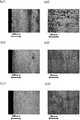
도 8a 및 도 8b는 반도체 기판의 광학 마이크로그래프들.
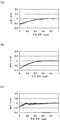
도 9a 및 도 9b는 각각 반도체 기판의 단차를 도시한 그래프들.
도 10a1, 도 10a2, 도 10b1, 도 10b2, 도 10c1, 및 도 10c2는 반도체 기판의 광학 마이크로그래프들.
도 11a1, 도 11a2, 도 11b1, 도 11b2, 도 11c1, 및 도 11c2는 반도체 기판의 광학 마이크로그래프들.
도 12a 내지 도 12c는 각각 반도체 기판의 단차를 도시한 그래프들.
도 13a 내지 도 13c는 각각 반도체 기판의 단차를 도시한 그래프들.
도 14a 내지 도 14c는 각각 반도체 기판의 단차를 도시한 그래프들.
도 15a 내지 도 15c는 각각 반도체 기판의 단차를 도시한 그래프들.
도 16a 내지 도 16c는 각각 반도체 기판의 단차를 도시한 그래프들.
도 17a 내지 도 17c는 각각 반도체 기판의 단차를 도시한 그래프들.
도 18a 내지 도 18c는 각각 반도체 기판의 단차를 도시한 그래프들.
도 19a 내지 도 19c는 각각 반도체 기판의 단차를 도시한 그래프들.
도 20a 내지 도 20c는 각각 반도체 기판의 단차를 도시한 그래프들.
도 21a 내지 도 21c는 각각 반도체 기판의 단차를 도시한 그래프들.
도 22a 내지 도 22c는 각각 반도체 기판의 단차를 도시한 그래프들.
도 23a 내지 도 23c는 각각 반도체 기판의 단차를 도시한 그래프들.
도 24는 에칭 시간 및 에칭 양 간의 관계를 도시한 도면.
도 25a 및 도 25b는 반도체 기판의 광학 마이크로그래프들.
도 26a 및 도 26b는 각각 반도체 기판의 단차를 도시한 그래프들.
도 27a 및 도 27b는 반도체 기판의 단면 TEM 이미지들.
도 28a 및 도 28b는 반도체 기판의 광학 마이크로그래프들.1A to 1D are cross-sectional views illustrating a method of regeneration processing for a semiconductor substrate.
2A and 2B are enlarged views of steps of a semiconductor substrate;
Figures 3A-3C are cross-sectional views illustrating a method for fabricating an SOI substrate.
Figures 4A-4C are cross-sectional views illustrating a method for fabricating an SOI substrate.
Figures 5A-5C are cross-sectional views illustrating a method for fabricating an SOI substrate.
6 is a view showing a manufacturing process of an SOI substrate;
7 is a sectional view showing a semiconductor device including an SOI substrate.
8A and 8B are optical micrographs of a semiconductor substrate.
9A and 9B are graphs showing step differences of a semiconductor substrate, respectively.
10A1, 10A2, 10B1, 10B2, 10C1, and 10C2 are optical micrographs of a semiconductor substrate.
11A1, 11A2, 11B1, 11B2, 11C1, and 11C2 are optical micrographs of a semiconductor substrate.
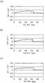
12A to 12C are graphs showing step differences of a semiconductor substrate, respectively.
13A to 13C are graphs showing step differences of the semiconductor substrate, respectively.
14A to 14C are graphs showing step differences of the semiconductor substrate, respectively.
15A to 15C are graphs showing step differences of the semiconductor substrate, respectively.
16A to 16C are graphs showing step differences of a semiconductor substrate, respectively.
FIGS. 17A to 17C are graphs showing step differences of a semiconductor substrate, respectively. FIG.
18A to 18C are graphs showing step differences of the semiconductor substrate, respectively.
19A to 19C are graphs showing step differences of a semiconductor substrate, respectively.
20A to 20C are graphs showing step differences of a semiconductor substrate, respectively.
FIGS. 21A to 21C are graphs showing step differences of a semiconductor substrate, respectively. FIG.
22A to 22C are graphs showing step differences of the semiconductor substrate, respectively.
23A to 23C are graphs showing step differences of the semiconductor substrate, respectively.
24 is a view showing a relationship between an etching time and an etching amount;
25A and 25B are optical micrographs of a semiconductor substrate.
26A and 26B are graphs showing step differences of the semiconductor substrate, respectively.
27A and 27B are cross-sectional TEM images of a semiconductor substrate.
28A and 28B are optical micrographs of a semiconductor substrate.
실시예들 및 예들이 이제 도면들을 참조하여 이하에서 기술될 것이다. 본 발명은 많은 상이한 모드들로 구현될 수 있으며, 상기 모드들 및 상세들은 본 발명의 사상 및 범위로부터 벗어나지 않고 다양한 방식들로 변경될 수 있음을 이 기술분야의 숙련자들에게 명백함을 주의하자. 그러므로, 본 발명은 상기 실시예들 및 상기 예들의 설명에 제한되는 것으로 해석되어서는 안된다. 동일한 부분들 또는 유사한 기능을 갖는 부분들은 이러한 명세 등에서 동일한 참조 부호들로 표시되며 그 설명은 몇몇 경우들에서 생략됨을 주의하자.Embodiments and examples will now be described with reference to the drawings. It should be noted that the present invention can be implemented in many different modes, and that the modes and details are susceptible to variations in various ways without departing from the spirit and scope of the invention. Therefore, the present invention should not be construed as being limited to the embodiments and descriptions of the above examples. It is to be noted that parts having the same or similar functions are denoted by the same reference numerals in these specifications and the description is omitted in some cases.
[실시예 1][Example 1]
이 실시예에서, 반도체 기판을 재생하기 위한 방법이 도 1a 내지 도 1d, 도 2a 및 도 2b를 참조하여 기술될 것이다.In this embodiment, a method for regenerating a semiconductor substrate will be described with reference to Figs. 1A to 1D, 2A and 2B.
도 1a는 재생 처리(반도체층이 분리되는 반도체 기판) 전에 반도체 기판(121)의 구조에 대한 일 예를 도시한다. 단차부(126)가 상기 반도체 기판(121)의 주변부에 존재한다. 상기 단차부(126)는 절연층(123), 분리되지 않은 반도체 영역(125), 및 반도체 영역(127)을 포함한다. 상기 분리되지 않은 반도체 영역(125) 및 상기 반도체 영역(127) 둘 모두는 손상되며 SOI 기판의 제조 프로세스에서 이온 조사 처리 등으로 인한 많은 결정 결함들, 보이드들, 블리스터들 등을 포함함을 주의하자. 특히, 상기 반도체 영역(127)은 상기 이온 조사로 인한 손상 및 취화가 두드러지는 영역이다. 그러므로, 상기 분리되지 않은 반도체 영역(125) 및 상기 반도체 영역(127)은 손상된 반도체 영역으로서 총괄하여 일컬어질 수 있다. 예를 들면, 단결정 반도체 기판의 경우에서, 상기 손상된 반도체 영역은 결정(결정 구조)에서 원자들의 정렬의 무질서, 결정 결함, 결정 격자의 왜곡 등을 포함하는 영역 부분을 나타내고, 이는 이온 조사 등에 의해 야기되는 반면, 단결정 반도체 영역은 결정에서의 원자들이 공간적으로 규칙적인 방식으로 정렬되는 영역이다. 게다가, 비손상된 반도체 영역은 결정에서의 원자들이 공간적으로 정렬된 방식으로 정렬되고 이온들 등으로 조사되지 않는 단결정 반도체 영역과 동일한 품질을 갖는 단결정 반도체 영역을 나타낸다.1A shows an example of the structure of the
상기 단차부(126)는 상기 반도체 기판의 소위 에지 롤 오프(E. R. O.) 영역을 포함한다. 상기 에지 롤 오프 영역은 상기 반도체 기판의 표면 처리(CMP 처리)에 의해 야기된다. 상기 반도체 기판의 상기 에지 롤 오프 영역은 상기 반도체 기판의 중심 영역보다 작은 두께를 가지기 때문에, 접합은 SOI 기판을 제조할 때 상기 에지 롤 오프 영역에서 수행되지 않는다. 그 결과, 상기 단차부(126)가 상기 반도체 기판(121)의 상기 에지 롤 오프 영역에 남겨진다.The
이온들로 조사된 반도체 영역(129)은 상기 단차부(126) 외의 상기 반도체 기판(121)의 영역에(특히, 상기 에지 롤 오프 영역에 의해 둘러싸여진 영역에) 존재한다. 상기 반도체 영역(129)은 상기 SOI 기판의 제조 프로세스에서 형성되는 이온들로 조사된 영역의 일부가 상기 반도체층이 분리된 후 상기 반도체 기판(121)에 남겨지는 방식으로 형성된다.The
여기에서, 상기 반도체 영역(129)은 상기 단차부(126)에서의 상기 반도체 영역들(상기 반도체 영역(125) 및 상기 반도체 영역(127))과 비교하여 충분히 얇다. 더욱이, 상기 반도체 영역(129)은 이온 조사 처리 등에 의해 손상되며 많은 결정 결함들 등을 포함한다. 그러므로, 상기 반도체 영역(125) 및 상기 반도체 영역(127)뿐만 아니라 상기 반도체 영역(129)은 손상된 반도체 영역으로서 칭하여질 수 있다.Here, the
도 2a는 상기 단차부(126)가 확대되는 개략도를 도시한다. 상기 단차부(126)는 상기 에지 롤 오프 영역에 대응하는 영역 및 챔퍼부(chamfer portion)에 대응하는 영역을 포함한다. 이 실시예에서, 상기 에지 롤 오프 영역은 상기 단차부(126)의 표면의 접평면 및 기준면 사이의 각도가 0.5° 이하가 되는 점들이 집합된 것을 말한다. 여기에서, 상기 기준면으로서, 상기 반도체 기판의 전면 또는 후면에 평행인 평면이 채용된다.2A shows a schematic view in which the
대안적으로, 상기 챔퍼부로서 상기 기판의 단부로부터 0.2mm의 거리에 영역을 설정함으로써, 상기 에지 롤 오프 영역은 상기 챔퍼부 안에 있고 접합이 수행되지 않는 영역으로서 정의될 수 있다. 상세하게는, 예를 들면, 상기 기판의 단부로부터 0.2mm 내지 0.9mm의 거리에서의 영역은 상기 에지 롤 오프 영역으로서 칭하여질 수 있다.Alternatively, by setting the region at a distance of 0.2 mm from the end of the substrate as the chamber portion, the edge roll-off region can be defined as the region in the chamber portion where bonding is not performed. In detail, for example, a region at a distance of 0.2 mm to 0.9 mm from the end of the substrate can be referred to as the edge roll-off region.
상기 챔퍼부는 베이스 기판 및 접합 기판 사이의 접합에 영향을 미치지 않음을 주의하자. 그러므로, 상기 챔퍼부의 평탄도는 상기 기판의 재생 처리에서 문제가 아니다. 다른 한편, 상기 에지 롤 오프 영역의 부근은 상기 베이스 기판 및 상기 접합 기판 사이의 상기 접합에 대해 영향을 미친다. 그러므로, 재생된 반도체 기판은 몇몇 경우들에서, SOI 기판의 제조 프로세스에서 사용될 수 없으며, 이것은 상기 에지 롤 오프 영역의 평탄도에 의존한다. 이러한 이유로, 상기 그 평탄도가 상기 반도체 기판의 상기 재생 처리에서 개선되도록 상기 에지 롤 오프 영역에서 상기 단차부(126)를 제거하는 것은 매우 중요하다.Note that the chamfered portion does not affect the bonding between the base substrate and the bonded substrate. Therefore, the flatness of the chamfered portion is not a problem in the regeneration processing of the substrate. On the other hand, the vicinity of the edge roll-off region affects the bonding between the base substrate and the bonded substrate. Therefore, the regenerated semiconductor substrate can not be used in the manufacturing process of the SOI substrate in some cases, which depends on the flatness of the edge roll-off region. For this reason, it is very important to remove the
도 2b는 도 1a에 도시된 단차부(128)가 확대되는 개략도를 도시한다. 상기 분리되지 않은 반도체 영역(125) 및 상기 반도체 영역(127) 둘 모두는 손상되며 SOI 기판의 제조 프로세스에서 이온들의 조사 처리 등으로 인한 많은 결정 결함들, 보이드들, 블리스터들(134) 등을 포함한다. 점선에 의해 둘러싸인 영역(135)은 상기 블리스터들 위의 상기 절연막 및 상기 반도체층이 손상되는 상태를 도시한다. 다수의 볼록부들 및 오목부들이 상기 절연층(123)의 표면상에 존재한다.Fig. 2B shows a schematic view in which the stepped
상기 반도체 기판의 재생 처리는 적어도 상기 절연층(123)을 제거하기 위한 에칭 처리(이하에서는 제 1 에칭 처리로서 불리움), 상기 손상된 반도체 영역을 제거하기 위한 에칭 처리(이하에서는 제 2 에칭 처리로서 불리움), 및 상기 제 2 에칭 처리 후 상기 반도체 기판을 평탄화하기 위한 열 처리를 포함한다. 이들은 이하에서 상세히 기술된다.The regeneration treatment of the semiconductor substrate includes an etching treatment for removing at least the insulating layer 123 (hereinafter referred to as a first etching treatment), an etching treatment for removing the damaged semiconductor region (hereinafter referred to as a second etching treatment) And a heat treatment for planarizing the semiconductor substrate after the second etching treatment. These are described in detail below.
첫째로, 상기 제 1 에칭 처리는 도 1a를 참조하여 기술된다. 상술된 바와 같이, 상기 제 1 에칭 처리는 상기 반도체 기판(121)으로부터 상기 절연층(123)을 제거하기 위한 에칭 처리이다. 여기에서, 상기 절연층(123)은 에천트로서 플루오르화 수소산을 포함하는 용액을 사용하여 웨트 에칭 처리에 의해 제거될 수 있다. 플루오르화 수소산을 포함한 용액으로서, 플루오르화 수소산, 플루오르화 암모늄, 및 계면 활성제(예로서, 제품명: 스텔라 케미파 코포레이션(Stella Chemifa Corporation)에 의해 제조된 LAL(500)) 등을 포함한 혼합액이 사용되는 것이 바람직하다. 이러한 웨트 에칭 처리는 바람직하게는 20초들 내지 1200초들, 예를 들면 대략 300초들 동안 수행된다.First, the first etching process is described with reference to FIG. 1A. As described above, the first etching process is an etching process for removing the insulating
웨트 에칭 처리는 상기 반도체 기판(121)이 처리 탱크에서의 용액에 담궈지는 방식으로 수행될 수 있기 때문에, 복수의 반도체 기판들(121)은 즉시 처리될 수 있다. 따라서, 상기 재생 처리의 효율성이 증가될 수 있다. 또한, 상기 절연층(123)은 상기 제 1 에칭 처리에 의해 제거되고 상기 제 2 에칭 처리에 의해 제거될 필요가 없기 때문에, 상기 에칭 시간은 단축될 수 있다. 더욱이, 상기 반도체는 상기 제 1 에칭 처리에 의해 거의 에칭되지 않기 때문에, 상기 에칭에 의해 제거된 상기 반도체 기판(121)의 양은 감소될 수 있으며 상기 재생 횟수들은 증가될 수 있다.Since the wet etching process can be performed in such a manner that the
상기 제 1 에칭 처리에서, 드라이 에칭 처리는 상기 절연층(123)이 제거될 수 있는 한 채용될 수 있다. 대안적으로, 웨트 에칭 처리 및 드라이 에칭 처리가 결합하여 사용될 수 있다. 상기 드라이 에칭 처리에 대해, 평행 평판 반응성 이온 에칭(RIE) 방법, 유도적으로 결합된 플라즈마(ICP) 에칭 방법 등이 사용될 수 있다.In the first etching process, the dry etching process can be employed as long as the insulating
다음으로, 상기 제 2 에칭 처리는 도 1b를 참조하여 기술된다. 상기 제 2 에칭 처리에서, 상기 손상된 반도체 영역들, 즉 상기 단차부(126)에 포함된 상기 분리되지 않은 반도체 영역(125) 및 상기 반도체 영역(127), 및 이온들로 조사된 상기 반도체 영역(129)이 선택적으로 제거된다. 보다 상세하게는, 웨트 에칭 처리가 에천트로서 반도체 재료를 산화시키는 물질, 상기 산화된 반도체 재료를 용해시키는 물질, 및 상기 반도체 재료의 산화 속도 및 상기 산화된 반도체 재료의 용해 속도를 제어하는 물질을 포함하는 혼합액을 사용하여 수행된다.Next, the second etching process is described with reference to Fig. 1B. In the second etching process, the damaged semiconductor regions, that is, the
상기 처리에서, 질산은 바람직하게는 상기 반도체 재료를 산화시키는 상기 물질을 포함하는 화학 용액을 위해 사용된다. 플루오르화 수소산은 바람직하게는 상기 산화된 반도체 재료를 용해시키는 상기 물질을 포함한 화학 용액을 위해 사용된다. 아세트산은 바람직하게는 상기 반도체 재료의 산화 속도 및 상기 산화된 반도체 재료의 용해 속도를 제어하는 상기 물질을 포함한 화학 용액을 위해 사용된다. 상기 에천트의 조성은 바람직하게는 다음과 같이 설정된다. 70 중량% 질산의 볼륨은 97.7 중량% 아세트산의 0.01배 이상이고 1배 미만이며 50 가중 % 플루오르화 수소산의 0.1배 이상이고 100배 미만이며, 상기 50 중량% 플루오르화 수소산의 볼륨은 97.7 중량% 아세트산의 0.01배 이상이고 0.5배 이하이다. 예를 들면, 상기 플루오르화 수소산, 질산, 및 아세트산의 체적비는 1:3:10, 1:2:10, 1.5:3:10 등인 것이 바람직하다. 상기 체적비 1:3:10은 분자들의 몰비로 HF;HNO3:CH3COOH:H2O = 2.05:3.29:11.55:7.42로서 표현된다. 다른 분자들의 구성에 대한 특별한 제한은 없다. 상기 에칭 처리는 바람직하게는 대략 1분 내지 20분들 동안 수행된다. 예를 들면, 상기 에칭 처리는 바람직하게는 플루오르화 수소산, 질산, 및 아세트산의 체적비가 1:3:10인 경우에 대략 2분 내지 4분 동안 그리고 플루오르화 수소산, 질산, 및 아세트산의 체적비가 1:2:10인 경우에 대략 6분 내지 12분 동안 수행된다. 또한, 상기 혼합액의 온도는 대략 10℃ 내지 30℃, 예를 들면 22℃ 내지 23℃인 것이 바람직하다.In this process, nitric acid is preferably used for the chemical solution comprising the material to oxidize the semiconductor material. The hydrofluoric acid is preferably used for a chemical solution containing said material to dissolve said oxidized semiconductor material. The acetic acid is preferably used for a chemical solution containing the material to control the oxidation rate of the semiconductor material and the dissolution rate of the oxidized semiconductor material. The composition of the etchant is preferably set as follows. The volume of 70 wt% nitric acid is 0.01 times or more of 97.7 wt% acetic acid and less than 1 time, more than 0.1 times and less than 100 times of 50 wt% hydrofluoric acid, and the volume of the 50 wt% hydrofluoric acid is 97.7 wt% 0.01 times or more and 0.5 times or less. For example, the volume ratio of hydrofluoric acid, nitric acid, and acetic acid is preferably 1: 3: 10, 1: 2: 10, 1.5: 3: 10, The volume ratio of 1: 3: 10 molar ratio of HF in themolecule; HNO 3: CH 3 COOH: H 2 O = 2.05: 3.29: 11.55: is expressed as 7.42. There are no particular restrictions on the construction of other molecules. The etching treatment is preferably performed for about 1 to 20 minutes. For example, the etch process is preferably performed for about 2 to 4 minutes with a volume ratio of hydrofluoric acid, nitric acid, and acetic acid of 1: 3: 10 and a volume ratio of hydrofluoric acid, nitric acid, : 2: 10 for about 6 to 12 minutes. Further, the temperature of the mixed liquid is preferably about 10 캜 to 30 캜, for example, 22 캜 to 23 캜.
비를 사용하는 상기 표현들에서, 상기 화학 용액들 또는 상기 분자 수들 각각은 ±10%의 에러 마진을 갖는다. 예를 들면, 플루오르화 수소산, 질산, 및 아세트산의 체적비가 1:3:10인 표현에서, x:y:z(플루오르화 수소산(x), 질산(y), 및 아세트산(z))은 x=0.9 내지 1.1, y=2.7 내지 3.3, 및 z=9 내지 11의 범위에 있을 수 있다. 유사하게는, 플루오르화 수소산, 질산, 및 아세트산의 체적비가 1:2:10인 표현에서, x:y:z(플루오르화 수소산(x), 질산(y), 및 아세트산(z))는 x=0.9 내지 1.1, y=1.8 내지 2.2, 및 z=9 내지 11의 범위에 있을 수 있다.In the above expressions using the ratios, each of the chemical solutions or the number of molecules has an error margin of +/- 10%. For example, x: y: z (hydrofluoric acid (x), nitric acid (y), and acetic acid (z)) in the expression that the volume ratio of hydrofluoric acid, nitric acid, and acetic acid is 1: 3: = 0.9 to 1.1, y = 2.7 to 3.3, and z = 9 to 11. Similarly, x: y: z (hydrofluoric acid (x), nitric acid (y), and acetic acid (z)) in the expression that the volume ratio of hydrofluoric acid, nitric acid, and acetic acid is 1: 2: = 0.9 to 1.1, y = 1.8 to 2.2, and z = 9 to 11.
이온 조사로 인한 결정 결함들, 보이드들, 블리스터들 등은 상기 손상된 반도체 영역에 존재하며, 에천트는 그 안으로 쉽게 침투한다. 따라서, 상기 손상된 반도체 영역에서, 웨트 에칭 처리는 표면으로부터 뿐만 아니라 내부로부터 또한 진행한다. 상세하게는, 상기 에칭은 깊은 홀(hole)이 상기 기판의 평면에 수직인 방향으로 형성되고 그 후 상기 홀이 확대되는 방식으로 진행하려는 경향이 있다. 달리 말하면, 상기 손상된 반도체 영역에서, 상기 에칭 처리는 덜-손상된 반도체 영역 또는 상기 비손상된 반도체 영역에서보다 높은 에칭 레이트로 진행한다. 여기서, "에칭 레이트"는 단위 시간당 상기 에칭 양(에칭된 양)을 의미한다. 또한, "에칭 선택비"는 두 개의 상이한 층들이 에칭되는 경우에서, 각 층의 에칭 레이트의 비를 의미한다. 또한, 상기 덜-손상된 반도체 영역은 상기 손상도가 상기 분리되지 않은 반도체 영역(125), 상기 반도체 영역(127), 이온들로 조사된 상기 반도체 영역(129) 등의 것과 비교하여 비교적 낮은 반도체 영역을 말한다.Crystal defects, voids, blisters, etc. due to ion irradiation are present in the damaged semiconductor region, and the etchant easily penetrates into it. Thus, in the damaged semiconductor region, the wet etching process proceeds not only from the surface but also from the inside. In particular, the etching tends to proceed in such a way that a deep hole is formed in a direction perpendicular to the plane of the substrate and then the hole is enlarged. In other words, in the damaged semiconductor region, the etching process proceeds at a higher etch rate in the less-damaged semiconductor region or the intact semiconductor region. Here, "etching rate" means the amount of etching per unit time (amount of etching). The "etch selectivity ratio" also means the ratio of the etch rate of each layer in the case where two different layers are etched. In addition, the less-damaged semiconductor region may have a degree of damage lower than that of the
보다 상세하게는, 상기 손상된 반도체 영역의 에칭 레이트는 상기 비손상된 반도체 영역(또는 상기 덜-손상된 반도체 영역)의 두 배 이상 높다. 즉, 상기 비손상된 반도체 영역(또는 상기 덜-손상된 반도체 영역)에 대한 상기 손상된 반도체 영역의 에칭 선택비는 2 이상이다.More particularly, the etch rate of the damaged semiconductor region is at least twice as high as that of the intact semiconductor region (or the less-damaged semiconductor region). That is, the etch selectivity ratio of the damaged semiconductor region to the intact semiconductor region (or the less-damaged semiconductor region) is two or more.
이러한 방식으로, 상기 웨트 에칭 처리가 에천트로서, 상기 반도체 재료를 산화시키는 상기 물질, 상기 산화된 반도체 재료를 용해시키는 상기 물질, 및 상기 반도체 재료의 산화 속도 및 상기 산화된 반도체 재료의 용해 속도를 제어하는 상기 물질을 포함하는 혼합액을 사용하여 수행되며, 상기 손상된 반도체 영역은 선택적으로 제거될 수 있다. 따라서, 상기 재생 처리에서 제거된 상기 반도체의 양은 감소될 수 있으며, 재생 및 사용의 횟수들이 증가될 수 있다. 더욱이, 상기 웨트 에칭 처리에 의해, 복수의 반도체 기판들(121)이 즉시 처리될 수 있다. 그러므로, 상기 재생 처리의 효율성이 증가될 수 있다. 더욱이, 상기 제 2 에칭 처리가 단기간에 수행될 수 있기 때문에, 상기 재생 처리의 효율성이 또한 이러한 이유로 증가될 수 있다.In this manner, the wet etch process may include, as an etchant, the material that oxidizes the semiconductor material, the material that dissolves the oxidized semiconductor material, and the rate of oxidation of the semiconductor material and the rate of dissolution of the oxidized semiconductor material And the damaged semiconductor region can be selectively removed. Therefore, the amount of the semiconductor removed in the regeneration process can be reduced, and the number of times of regeneration and use can be increased. Moreover, by the wet etching treatment, the plurality of
상기 단차부(126)(상기 반도체 영역(125) 및 상기 반도체 영역(127))에서 상기 손상된 반도체 영역의 두께는 상기 다른 영역(상기 반도체 영역(129))에서 상기 손상된 반도체 영역의 것과 크게 상이하다. 그러므로, 상기 다른 영역(상기 중심부)에 대한 상기 단차부(126)(상기 주변부)의 상기 에칭 선택비는 상기 제 2 에칭 처리 동안 균일하지 않다.The thickness of the damaged semiconductor region in the step 126 (the
세부사항들이 이하에 기술된다. 상기 제 2 에칭 처리가 시작된 직후, 상기 손상된 반도체 영역은 먼저 상기 단차부(126) 및 상기 다른 영역 모두에서 에칭된다; 따라서, 상기 에칭 선택비는 유사해진다(상세하게는, 대략 1). 상기 단차부(126)(상기 반도체 영역(129))와 다른 영역에서의 상기 손상된 반도체 영역이 제거되도록 에칭된 후, 상기 덜-손상된 반도체 영역 또는 상기 비손상된 반도체 영역은 상기 단차부(126)와 다른 영역에서 노출된다; 따라서, 상기 덜-손상된 반도체 영역 또는 상기 비손상된 반도체 영역의 에칭 레이트가 감소된다. 그러므로, 상기 단차부(126)에서 상기 손상된 반도체 영역은 우선적으로 제거되며, 상기 덜-손상된 반도체 영역 또는 상기 비손상된 반도체 영역에 대한 상기 손상된 반도체 영역의 에칭 선택비는 높아진다(특히, 2 이상). 상기 단차부(126)(상기 반도체 영역(125) 및 상기 반도체 영역(127))에서 상기 손상된 반도체 영역이 제거되게 에칭된 후, 상기 덜-손상된 반도체 영역 또는 상기 비손상된 반도체 영역이 또한 상기 단차부(126)에서 노출되고; 따라서, 상기 에칭 선택비는 다시 유사해진다(상세하게는, 대략 1).Details are described below. Immediately after the second etching process is started, the damaged semiconductor region is first etched in both the
이러한 방식으로, 상기 에칭 선택비는 상기 제 2 에칭 처리 동안 변하기 때문에, 상기 에칭은 상기 에칭 선택비를 고려하여 피니싱(finish)될 수 있다. 예를 들면, 상기 덜-손상된 반도체 영역 또는 상기 비손상된 반도체 영역에 대한 상기 손상된 반도체 영역의 에칭 선택비가 2보다 낮게 감소되는 단계에서 상기 에칭 처리를 정지함으로써, 상기 손상된 반도체 영역은 상기 제 2 에칭 처리에 의해 제거된 상기 반도체의 양이 감소되는 동안 제거될 수 있다. 이러한 경우에, 상기 재생 처리는 확실히 수행될 수 있고 재생 횟수들은 충분히 확보될 수 있다. 상기 에칭 선택비는 미리 정해진 시간(예로서, 30초들 또는 1분)에 감소된 두께의 양들을 비교함으로써 획득된 값(차분값) 또는 순간 감소된 두께의 양들을 비교함으로써 획득된 값(미분값)일 수 있음을 주의해야 한다.In this way, since the etch selectivity varies during the second etch process, the etch may be finished taking into account the etch selectivity. For example, by stopping the etching process at a step in which the etch selectivity of the damaged semiconductor region to the less-damaged semiconductor region or the undamaged semiconductor region is reduced to less than 2, the damaged semiconductor region is subjected to the second etching process Lt; / RTI > can be removed while the amount of the semiconductor removed by the semiconductor device is reduced. In this case, the regeneration process can be reliably performed and the number of regeneration times can be sufficiently secured. The etch selectivity is a value obtained by comparing the amounts obtained by comparing the amounts of reduced thickness (difference value) or the amounts of the instant reduced thickness for a predetermined time (for example, 30 seconds or 1 minute) ). ≪ / RTI >
비록 여기에 도시되지 않았지만, 상기 단차부(126)는 상기 반도체층이 상기 반도체 기판(121)으로부터 분리되는 몇몇 경우들에서 손상되거나 또는 부분적으로 손상된다는 것을 주의해야 한다. 이러한 경우들에서, 상기 에천트는 상기 손상된 영역으로부터 상기 제 1 에칭 처리 및 상기 제 2 에칭 처리를 통해 그 주변부로 침투하며, 상기 비손상된 반도체 영역(또는 상기 덜-손상된 반도체 영역)에 남겨진 상기 손상된 반도체 영역은 선택적으로 제거된다.It should be noted that although not shown here, the
다음으로, 평탄화 처리가 상기 제 2 에칭 처리 후에 반도체 기판(130)상에서 수행되며, 따라서 재생된 반도체 기판(132)이 제조된다(도 1d를 참조). 상기 반도체 기판(130)이 도 1c에 도시된 바와 같이 상기 제 2 에칭 처리 후 상기 반도체 기판(130)의 표면이 충분한 평탄도를 갖지 않을 때 SOI 기판의 제조 프로세스에서 사용될 수 없기 때문에 이러한 처리가 수행된다. 이 실시예에서, 상기 반도체 영역(129)이 상기 제 2 에칭 처리에 의해 완전히 제거되는 경우가 기술되지만; 그러나, 상기 반도체 영역(129)이 상기 제 2 에칭 처리에 의해 충분히 제거될 수 없는 경우에, 상기 나머지 반도체 영역(129)은 이하에 기술된 평탄화 처리에 의해 함께 제거되는 것이 바람직하다는 것을 주의해야 한다.Next, a planarization process is performed on the
상기 평탄화 처리로서, 상기 제 2 에칭 처리 후 상기 반도체 기판(130)은 수소 분위기 하에서 1100℃ 이상 1300℃ 이하의 온도로 30분 이상 240분이하 동안 열 처리될 수 있다.As the planarization treatment, the
가열 수단으로서, RTA(rapid thermal anneal) 장치, 저항 가열로(resistance heating furnace), 마이크로웨이브 가열 장치 등이 사용될 수 있다.As the heating means, a rapid thermal annealing (RTA) apparatus, a resistance heating furnace, a microwave heating apparatus, or the like can be used.
상기 열 처리는 수소 분위기뿐만 아니라 아르곤 분위기 또는 수소 및 아르곤의 혼합물의 분위기 하에서 수행될 수 있다는 것을 주의해야 한다. 예를 들면, 상기 수소 및 아르곤의 혼합물의 분위기가 이용되는 경우에, 상기 열 처리는 그 체적이 가열로에 도입된 가스에 대해 90 vol% 이상 100 vol% 이하의 아르곤 분위기하에서 1100℃ 이상 1300℃ 이하의 온도로 30분 이상 240분 이하 동안 수행될 수 있다. 상기 열 처리가 수소 및 아르곤의 혼합물의 분위기 하에서 수행되는 경우에서, 상기 가열로에 도입된 상기 가스에 대한 수소의 비율은 예를 들면 바람직하게는 4 vol%일 수 있다.It should be noted that the heat treatment can be performed not only in a hydrogen atmosphere but also in an argon atmosphere or an atmosphere of a mixture of hydrogen and argon. For example, when the atmosphere of the mixture of hydrogen and argon is used, the heat treatment is performed at a temperature of 1100 ° C to 1300 ° C in an argon atmosphere of 90 vol% to 100 vol% At a temperature of 30 minutes or more and 240 minutes or less. In the case where the heat treatment is performed in an atmosphere of a mixture of hydrogen and argon, the ratio of hydrogen to the gas introduced into the heating furnace may preferably be, for example, 4 vol%.
상기 열 처리의 분위기는 상기에 제한되지 않으며, 다른 가스의 분위기가 상기 제 2 에칭 처리 후 상기 반도체 기판(130)의 표면이 상기 분위기하에서 평탄화될 수 있는 한 채용될 수 있음을 주의해야 한다.It should be noted that the atmosphere of the heat treatment is not limited to the above, and the atmosphere of another gas may be adopted as long as the surface of the
아르곤 분위기 또는 산소 및 질소의 혼합물의 분위기 하에서 또 다른 열 처리가 상기 수소 분위기 하에서의 상기 열 처리 전 또는 후 수행될 수 있음을 주의해야 한다. 상기 반도체 기판(130)에서 산소의 외방 확산(out-diffusion)이 이러한 열 처리를 수행함으로써 촉진되기 때문에, 상기 반도체 기판(130)에서의 격자들 간에 존재하는 산소의 농도들은 감소될 수 있고, 상기 반도체 기판에 대한 OSF(oxidation-induced stacking fault)의 생성이 억제될 수 있다.It should be noted that another heat treatment under an atmosphere of argon atmosphere or a mixture of oxygen and nitrogen may be performed before or after the heat treatment under the hydrogen atmosphere. Since the out-diffusion of oxygen in the
적어도 상기 열 처리가 상기 평탄화 처리로서 수행되는 경우가 이 실시예에서 기술되었지만, 이에 대한 제한 없이, CMP 방법과 같은 연마 처리가 평탄화 처리를 수행하기 위해 그와 결합될 수 있다는 것을 주의해야 한다. 연마 처리는 상기 열 처리 후 또는 전에 수행될 수 있다. CMP 방법을 사용한 상기 연마 처리는 한번 또는 복수회 수행될 수 있다. 연마 처리가 복수회 수행될 때, 예를 들면, 높은 연마 레이트를 갖는 제 1 연마가 수행되고 그 후 낮은 연마 레이트를 갖는 피니싱 연마가 수행되는 것이 바람직하다. 상기 제 1 연마에서, 폴리우테탄 연마 천이 바람직하게 사용되며, 슬러리(slurry)의 입경(grain diameter)은 바람직하게는 120nm 내지 180nm, 예를 들면, 대략 150nm이다. 상기 피니싱 연마에서, 바람직하게는 스웨이드 연마 천이 사용되며, 슬러리의 입경은 바람직하게는 45nm 내지 75nm, 예를 들면 대략 60nm이다. 또한, 상기 연마 처리가 상이한 연마 레이트들로 복수회 수행될 때, 상기 반도체 기판(130)은 단기간에 평탄화될 수 있다.It is noted that although at least the thermal treatment is performed as the planarization treatment in this embodiment, it should be noted that, without limitation thereto, the polishing treatment, such as the CMP method, can be combined with it to perform the planarization treatment. The abrasive treatment may be performed after or before the heat treatment. The polishing treatment using the CMP method can be performed once or plural times. When the polishing process is performed a plurality of times, it is preferable that, for example, a first polishing with a high polishing rate is performed and then a finishing polishing with a low polishing rate is performed. In the first polishing, a polyurethane polishing cloth is preferably used, and the grain diameter of the slurry is preferably 120 nm to 180 nm, for example, approximately 150 nm. In the finishing polishing, preferably a suede polishing cloth is used, and the particle size of the slurry is preferably 45 nm to 75 nm, for example, approximately 60 nm. Further, when the polishing process is performed plural times at different polishing rates, the
상기 반도체 기판(130)의 표면은 상기 열 처리를 통해 평탄화되며, 그러므로 0.2nm 이하, 바람직하게는 0.1nm 이하의 평균면 거칠기(Ra)를 갖도록 평탄화되는 상기 재생된 반도체 기판(132)이 제조될 수 있다(도 1d를 참조).The surface of the
이 실시예에서 기술된 바와 같이, 졀연층이 상기 제 1 에칭 처리를 통해 제거된 후, 상기 제 2 에칭 처리는 상기 반도체 재료를 산화시키는 상기 물질, 상기 산화된 반도체 재료를 용해시키는 상기 물질, 및 상기 반도체 재료의 산화 속도 및 상기 산화된 반도체 재료의 용해 속도를 제어하는 상기 물질을 포함하는 상기 혼합액을 사용하여 수행되며, 따라서 상기 반도체 기판의 주변에 남아있는 상기 손상된 반도체 영역은 선택적으로 제거될 수 있다. 그러므로, 제거된 반도체의 양이 감소될 수 있고, 상기 반도체 기판의 재생 및 사용의 횟수들은 증가될 수 있다. 또한, 상기 열 처리는 상기 손상된 반도체 영역이 선택적으로 제거된 후 수소를 포함한 분위기 하에 수행되며, 따라서 양호한 평탄도를 갖는 재생된 반도체 기판이 획득될 수 있다.As described in this embodiment, after the burned-in layer is removed through the first etching process, the second etching process is performed on the material that oxidizes the semiconductor material, the material that dissolves the oxidized semiconductor material, and Wherein the damaged semiconductor region remaining in the periphery of the semiconductor substrate is selectively removed by using the mixed liquid comprising the material that controls the rate of oxidation of the semiconductor material and the rate of dissolution of the oxidized semiconductor material have. Therefore, the amount of removed semiconductor can be reduced, and the number of times of regeneration and use of the semiconductor substrate can be increased. Further, the heat treatment is performed under an atmosphere containing hydrogen after the damaged semiconductor region is selectively removed, so that a regenerated semiconductor substrate having good flatness can be obtained.
이 실시예에서 기술된 구조는 다른 실시예들 중 임의의 실시예에 기술된 구조와 적절하게 결합하여 사용될 수 있다.The structure described in this embodiment can be used in appropriate combination with the structure described in any of the other embodiments.
(실시예 2)(Example 2)
이 실시예에서 SOI 기판을 제조하기 위한 방법에서, SOI 기판은 베이스 기판에 대한 접합 기판인 반도체 기판으로부터 분리된 반도체층을 접합시킴으로써 제조된다. 상기 반도체층이 분리되는 상기 반도체 기판은 재생 처리되며 접합 기판으로서 재사용된다. 이 실시예의 SOI 기판을 제조하기 위한 방법의 일 예가 도 2a 및 도 2b, 도 3a 내지 도 3c, 도 4a 내지 도 4c, 도 5a 내지 도 5c, 및 도 6의 SOI 기판의 제조 프로세스 차트를 참조하여 이하게 기술될 것이다.In the method for manufacturing an SOI substrate in this embodiment, an SOI substrate is manufactured by bonding a semiconductor layer separated from a semiconductor substrate which is a bonded substrate to a base substrate. The semiconductor substrate from which the semiconductor layer is separated is regenerated and reused as a bonded substrate. An example of a method for manufacturing the SOI substrate of this embodiment will be described with reference to the manufacturing process chart of the SOI substrate of Figs. 2A and 2B, Figs. 3A to 3C, 4A to 4C, 5A to 5C, and 6 Will be described below.
먼저, 베이스 기판과의 접합을 준비하기 위해 반도체 기판(100)에 취화 영역(104)을 형성하는 프로세스가 기술된다. 이러한 프로세스는 상기 반도체 기판(100)에 대한 처리에 관한 것이며, 도 6에서의 프로세스 A에 대응한다.First, a process of forming the
먼저, 상기 반도체 기판(100)이 준비된다(도 3a 및 도 6에서의 단계(A-1) 참조). 상기 반도체 기판(100)으로서, 예를 들면, 실리콘 등의 단결정 반도체 기판 또는 다결정 반도체 기판이 사용될 수 있다. 상업적으로 이용가능한 실리콘 기판들의 통상적인 예들은 직경 5인치(125mm), 직경 6인치(150mm), 직경 8인치(200mm), 직경 12인치(300mm), 및 직경 16인치(400mm)인 원형 실리콘 기판들을 포함한다. 또한, 실리콘 기판의 주변부에서, 도 2a에 도시된 바와 같은 치핑(chipping) 또는 크랙킹(cracking)을 방지하기 위한 챔퍼부(champer portion)가 존재한다. 상기 기판의 형상은 원형 형상에 제한되지 않으며, 직사각형 형상 등으로 처리되는 실리콘 기판이 또한 사용될 수 있다. 직사각형 단결정 실리콘 기판이 상기 반도체 기판(100)으로서 사용되는 경우가 이하에 기술된다.First, the
상기 반도체 기판(100)의 표면은 바람직하게는 황산/과산화수소 혼합물(SPM), 수산화암모늄/과산화수소 혼합물(APM), 염산/과산화수소 혼합물(HPM), 희석된 불화 수소산(DHF) 등을 적절하게 사용하여 세정된다. 또한, 희석된 불화 수소산 및 오존수는 상기 반도체 기판(100)의 표면을 세정하기 위해 대안적으로 사용될 수 있다.The surface of the
상기 반도체 기판(100)의 표면이 세정된 후, 절연층(102)이 상기 반도체 기판(100)(도 3b 및 도 6에서의 단계(A-2) 참조) 위에 형성된다. 상기 절연층(102)은 단일 절연막 또는 복수의 절연막들을 포함하는 적층을 사용하여 형성될 수 있다. 상기 절연층(102)이 구성요소로서, 산화 실리콘막, 질화 실리콘막, 산화질화 실리콘막, 또는 질화산화 실리콘막과 같은 실리콘을 포함하는 절연막을 사용하여 형성될 수 있다. 이 실시예에서, 산화 실리콘막이 상기 절연층(102)으로서 사용되는 경우가 예로서 기술된다.After the surface of the
이러한 명세 등에서, 산화질화 실리콘막은 질소 원자들보다 많은 산소 원자들을 포함하고, 그것들이 러더퍼드 후방 산란법(Rutherford backscattering spectrometry; RBS) 및 수소 전방 산란법(hydrogen forward scattering spectrometry; HFS)에 의해 측정될 때, 각각 50 원자% 내지 70 원자%, 0.5 원자% 내지 15 원자%, 25 원자% 내지 35 원자%, 및 0.1 원자% 내지 10 원자%의 범위에 있는 농도로 산소, 질소, 실리콘, 및 수소를 포함하는 막을 의미한다. 또한, 질화산화 실리콘막은 산소 원자들보다 많은 질소 원자들을 포함하고, 그것들이 RBS 및 HFS에 의해 측정될 때, 각각 5 원자% 내지 30 원자%, 20 원자% 내지 55 원자%, 25 원자% 내지 35 원자%, 및 10 원자% 내지 30 원자%의 범위에 있는 농도들로 산소, 질소, 실리콘, 및 수소를 포함하는 막을 의미한다. 질소, 산소, 실리콘, 및 수소의 퍼센티지들은 산화질화 실리콘막 또는 질화산화 실리콘막에 포함된 원자들의 총 수가 100 원자%로서 정의될 때 상기 주어진 범위들 내에 속한다는 것을 주의해야 한다.In such specifications, when the silicon oxynitride film contains more oxygen atoms than nitrogen atoms and they are measured by Rutherford backscattering spectrometry (RBS) and hydrogen forward scattering spectrometry (HFS) Nitrogen, silicon, and hydrogen at concentrations ranging from 50 atomic percent to 70 atomic percent, 0.5 atomic percent to 15 atomic percent, 25 atomic percent to 35 atomic percent, and 0.1 atomic percent to 10 atomic percent, respectively, . Further, the silicon nitride oxide film contains more nitrogen atoms than oxygen atoms, and when they are measured by RBS and HFS, each of 5 atom% to 30 atom%, 20 atom% to 55 atom%, 25 atom% to 35 Means a film containing oxygen, nitrogen, silicon, and hydrogen at concentrations in the range of 10 atomic% to 10 atomic% to 30 atomic%. It should be noted that the percentages of nitrogen, oxygen, silicon, and hydrogen fall within the ranges given above when the total number of atoms contained in a silicon oxynitride film or a silicon nitride oxide film is defined as 100 atomic%.
산화 실리콘막이 상기 절연층(102)으로서 사용되는 경우에, 상기 절연층(102)은 열적 CVD법, 플라즈마 CVD법, 대기압 CVD법, 또는 실란 및 산소의 혼합 가스, 테트라에톡시실란(TEOS) 및 산소의 혼합 가스 등을 사용한 바이어스 ECRCVD법과 같은 기상 증착법으로 형성될 수 있다. 이러한 경우에, 상기 절연층(102)의 표면은 산소 플라즈마 처리에 의해 치밀화될 수 있다.When the silicon oxide film is used as the insulating
대안적으로, 유기실란 가스를 사용한 화학 기상 증착법에 의해 형성되는 산화 실리콘막은 상기 절연층(102)으로서 사용될 수 있다. 유기실란 가스에 대해, 테트라에톡시실란(TEOS)(화학식 : Si(OC2H5)4), 테트라메틸실란(TMS)(화학식: Si(CH3)4), 테트라메틸시클로테트라실록산(TMCTS), 옥타메틸시클로테트라실록산(OMCTS), 헥사메틸디실라잔(HMDS), 트리에톡시실란(화학식 : SiH(OC2H5)3), 또는 트리스디메틸아미노실란(화학식 : SiH(N(CH3)2)3) 과 같은 실리콘-함유 화합물이 사용될 수 있다.Alternatively, a silicon oxide film formed by a chemical vapor deposition method using an organosilane gas may be used as the insulating
또한 대안적으로, 상기 절연층(102)은 상기 반도체 기판(100)을 산화시킴으로써 획득된 산화막을 사용하여 형성될 수 있다. 상기 산화막을 형성하기 위한 열 산화 처리는 드라이 산화일 수 있고, 할로겐-포함 가스가 부가되는 산화 분위기하에 수행될 수 있다. 상기 할로겐-포함 가스로서, HCl, HF, NF3, HBr, Cl2, ClF3, BCl3, F2, Br2 등으로부터 선택된 하나 또는 복수의 종류들의 가스들이 사용될 수 있다. 상기 절연층(102)은 도 3b에서의 상기 반도체 기판(100)을 커버하도록 형성되지만; 이 실시예는 이러한 구조에 제한되지 않음을 주의해야 한다. 상기 절연층(102)이 상기 반도체 기판(100)에 걸쳐 CVD법 등으로 형성되는 경우에, 상기 절연층(102)은 상기 반도체 기판(100)의 표면들 중 단지 하나에 걸쳐 형성될 수 있다.Alternatively, the insulating
상기 열 산화막의 형성 조건들의 일 예로서, 열 처리는 산소에 대해 0.5 vol% 내지 10 vol%(바람직하게는 3 vol%)의 레이트로 HCl을 포함하는 분위기하에 700℃ 이상 1100℃ 이하로(통상적으로, 대략 950℃) 수행된다. 처리 시간은 0.1시간 내지 6시간들, 바람직하게는, 0.5시간 내지 1시간일 수 있다. 상기 형성될 산화막의 두께는 10nm 내지 1100nm의 범위(바람직하게는, 50nm 내지 150nm), 예를 들면 100nm에서 설정될 수 있다.As one example of conditions for forming the thermal oxide film, the heat treatment is performed at a temperature of 700 ° C or more and 1100 ° C or less (typically, at a rate of 0.5 vol% to 10 vol% (preferably 3 vol% Approximately 950 < 0 > C). The treatment time may be from 0.1 hour to 6 hours, preferably from 0.5 hour to 1 hour. The thickness of the oxide film to be formed may be set in the range of 10 nm to 1100 nm (preferably 50 nm to 150 nm), for example, 100 nm.
할로겐 원소를 포함하는 분위기 하의 이와 같은 열 산화 처리에 의해, 외인성 불순물(예로서, Fe, Cr, Ni, 또는 Mo)인 중금속이 제거될 수 있다.By such a thermal oxidation treatment under an atmosphere containing a halogen element, a heavy metal which is an extraneous impurity (for example, Fe, Cr, Ni or Mo) can be removed.
또한, 염소와 같은 할로겐 원소를 포함하는 상기 절연층(102)은 상기 반도체 기판(100)에 악영향을 주는 불순물들을(예로서, Na의 가동 이온들 등) 게터(getter)할 수 있다. 상세하게는, 상기 절연층(102)이 형성된 후 수행되는 열 처리에 의해, 상기 반도체 기판(100)에 포함된 불순물들이 상기 절연층(102)에 분리되고, 할로겐 원자들(예로서, 염소 원자들)과 반응되며, 캡처된다. 따라서, 상기 절연층(102)에 캡처된 상기 불순물들은 고정될 수 있으며, 상기 반도체 기판(100)을 오염시키는 것을 방지할 수 있다. 더욱이, 상기 절연층(102)이 유리 기판에 접합될 때, 상기 절연층(102)은 또한 유리에 포함된 Na와 같은 불순물들을 고정시키기 위한 막으로서 기능할 수 있다.In addition, the insulating
특히, 할로겐을 포함하는 분위기 하의 열 처리에 의해 상기 절연층(102)에서의 염소와 같은 할로겐의 포함은 상기 반도체 기판(100)의 세정이 불충분하거나 또는 상기 반도체 기판(100)이 반복적으로 재생 처리가 되고 사용될 때 상기 반도체 기판(100)의 오염물들을 제거하는데 효과적이다.In particular, the inclusion of a halogen such as chlorine in the insulating
게다가, 상기 산화 처리 분위기에 포함된 상기 할로겐 원소는 상기 반도체 기판(100)의 표면상의 결함들을 종결한다; 그러므로, 상기 산화막 및 상기 반도체 기판(100) 사이의 인터페이스의 국소적 레벨 밀도는 감소될 수 있다.In addition, the halogen element included in the oxidation treatment atmosphere terminates defects on the surface of the
상기 절연층(102)에 포함된 상기 할로겐 원소는 상기 절연층(102)에 왜곡들을 만든다. 그 결과, 상기 절연층(102)의 물 흡수 레이트는 향상되고 물의 확산 레이트는 증가된다. 즉, 물이 상기 절연층(102)의 표면에 존재할 때, 상기 표면에 존재하는 상기 물은 빠르게 흡수되고 상기 절연층(102)으로 확산될 수 있다.The halogen element contained in the insulating
베이스 기판으로서, 알칼리 금속 또는 알칼리 토금속과 같은 반도체 장치의 신뢰성을 감소시키는 불순물들을 포함하는 유리 기판이 사용되는 경우에, 상기 절연층(102)은 바람직하게는 상기 베이스 기판에서의 상기 불순물들이 상기 SOI 기판의 상기 반도체층으로 확산하는 것을 방지할 수 있는 적어도 하나 이상의 막들을 포함한다. 이러한 막의 예들은 질화 실리콘막, 질화산화 실리콘막 등을 포함한다. 상기 절연층(102)에 포함된 이러한 막을 가지고, 상기 절연층(102)은 배리어 막(또한 블로킹 막으로서 일컬어지는)으로서 기능할 수 있다.When a glass substrate containing impurities that reduces the reliability of a semiconductor device such as an alkali metal or an alkaline earth metal is used as the base substrate, the insulating
예를 들면, 질화 실리콘막은 플라즈마 CVD 법과 같은 기상 증착법을 갖는 실란 및 암모늄의 혼합 가스를 사용하여 형성될 수 있다. 또한, 예를 들면, 질화산화 실리콘막은 플라즈마 CVD 법과 같은 기상 증착법으로 실란, 암모니아, 및 산소를 포함한 화합물(예로서, 산소, 일산화 이질소, 산화 질소, 이산화 질소 등)을 사용하여 형성될 수 있다.For example, the silicon nitride film may be formed using a mixed gas of silane and ammonium having a vapor deposition method such as a plasma CVD method. Further, for example, the silicon nitride oxide film can be formed using a compound containing silane, ammonia, and oxygen (for example, oxygen, nitrogen monoxide, nitrogen oxide, nitrogen dioxide, etc.) by vapor deposition such as plasma CVD .
예를 들면, 단일-층 구조를 갖는 배리어 막이 상기 절연층(102)으로서 형성되는 경우에, 상기 절연층(102)은 15nm 이상 300nm 이하의 두께를 갖는 질화 실리콘막 또는 질화산화 실리콘막을 사용하여 형성될 수 있다.For example, when a barrier film having a single-layer structure is formed as the insulating
2층 배리어 막이 상기 절연층(102)으로서 형성되는 경우에, 상기 상부층은 높은 배리어 특성을 갖는 절연막을 사용하여 형성된다. 상기 상부층의 절연막은 에를 들면, 15nm 내지 300nm의 두께를 가진 질화 실리콘막 또는 질화산화 실리콘막을 사용하여 형성될 수 있다. 이들 막들은 불순물 확산을 방지하기 위한 높은 블로킹 효과를 갖지만, 그 내부 응력 또한 높다. 그러므로, 상기 반도체 기판(100)과 접하는 상기 하부층의 절연막으로서, 상기 상부층의 상기 절연막의 응력을 경감하는 효과를 갖는 막이 선택되는 것이 바람직하다. 상기 상부층의 상기 절연막의 응력을 경감하는 효과를 가진 상기 절연막으로서, 산화 실리콘막, 산화질화 실리콘막, 상기 반도체 기판(100)을 열적으로 산화시킴으로써 형성된 열 산화막 등이 주어진다. 상기 하부층의 상기 절연막의 두께는 5nm 이상 200nm 이하일 수 있다.When a two-layer barrier film is formed as the insulating
예를 들면, 배리어 막으로서 기능하기 위한 상기 절연층(102)을 위해, 상기 절연층(102)은 바람직하게는 상기 상부층과 상기 하부층을 위한 산화 실리콘막과 질화 실리콘막, 산화질화 실리콘막과 질화 실리콘막, 산화 실리콘막과 질화산화 실리콘막, 산화질화 실리콘막과 질화산화 실리콘막 등의 조합을 사용하여 형성된다.For example, for the insulating
다음으로, 상기 반도체 기판(100)은 화살표들에 의해 표시된 바와 같이, 상기 절연층(102)을 통해 전계에 의해 가속화된 이온들을 포함한 이온 빔으로 조사된다. 따라서, 상기 취화 영역(104)은 상기 반도체 기판(100)(도 3c 및 도 6에서의 단계(A-3) 참조)의 표면으로부터 원하는 깊이에 있는 영역에 형성된다. 상기 취화 영역(104)이 형성된 깊이는 상기 이온들의 평균 관통 깊이와 실질적으로 동일하고, 상기 이온 빔의 가속화 에너지 및 상기 이온 빔의 입사각에 의해 조정될 수 있다. 또한, 상기 가속화 에너지는 가속 전압 등에 의해 조정될 수 있다. 이후에 상기 반도체 기판(100)으로부터 분리되는 반도체층(124)의 두께는 상기 취화 영역(104)이 형성되는 상기 깊이에 의해 결정된다. 상기 취화 영역(104)이 형성되는 상기 깊이는 예를 들면 10nm 이상 500nm 이하의, 바람직하게는 상기 반도체 기판(100)의 표면으로부터 50nm 이상 200nm 이하의 범위에서 설정될 수 있으며; 예를 들면, 상기 깊이는 바람직하게는 상기 반도체 기판(100)의 표면으로부터 대략 100nm이다. 이온들로의 조사는 이 실시예에서 상기 절연층(102)의 형성 후 수행되지만; 이에 제한되지 않고, 이온들로의 조사는 상기 절연층(102)의 형성 전에 수행될 수 있음을 주의해야 한다.Next, the
상기 취화 영역(104)은 이온 도핑 처리에 의해 형성될 수 있다. 상기 이온 도핑 처리는 이온 도핑 장치를 갖고 수행될 수 있다. 이온 도핑 장치의 통상적인 예는 챔버에 위치된 물체(object)가 프로세스 가스의 플라즈마로의 여기에 의해 생성된 모든 이온 성분들로 조사되는 비-질량-분리 장치이다. 상기 비-질량-분리 장치는 물체가 플라즈마에서 이온 성분들의 질량 분리 없이 모든 이온 성분들로 조사되는 장치이다.The
이온 도핑 장치의 주요 구성요소들은 다음과 같다: 물체가 위치되는 챔버; 원하는 이온들을 생성하기 위한 이온 소스; 및 그것과 함께 조사를 위한 이온들의 가속화를 위한 가속 메커니즘. 상기 이온 소스는 원하는 이온 성분들을 생성하기 위한 소스 가스, 플라즈마를 생성하기 위해 상기 소스 가스를 여기시키기 위한 전극 등을 공급하는 가스 공급 장치를 포함한다. 플라즈마를 생성하기 위한 상기 전극으로서, 용량-결합형 고-주파수 방전용 전극, 필라멘트 전극 등이 사용된다. 상기 가속 메커니즘은 추출 전극, 가속 전극, 감속 전극, 및 접지 전극과 같은 전극들; 전력을 이들 전극들에 공급하기 위한 전원 등을 포함한다. 상기 가속 메커니즘에 포함된 이들 전극들에는 복수의 개구들 또는 슬릿들이 제공되며, 이를 통해 상기 이온 소스로부터 생성되는 이온들이 가속된다. 상기 이온 도핑 장치의 구성요소들은 상술된 것들에 제한되지 않으며 필요에 따라 변경될 수 있음을 주의하자.The main components of the ion doping apparatus are as follows: a chamber in which an object is placed; An ion source for generating desired ions; And an acceleration mechanism for accelerating ions for irradiation therewith. The ion source includes a gas supply for supplying a source gas for generating desired ion components, an electrode for exciting the source gas to generate a plasma, and the like. As the electrode for generating the plasma, a capacitive-coupling type high-frequency discharge electrode, a filament electrode, or the like is used. The acceleration mechanism includes electrodes such as an extraction electrode, an acceleration electrode, a deceleration electrode, and a ground electrode; A power source for supplying power to these electrodes, and the like. The electrodes included in the acceleration mechanism are provided with a plurality of openings or slits through which ions generated from the ion source are accelerated. Note that the components of the ion doping apparatus are not limited to those described above, and may be changed as needed.
이 실시예에서, 상기 반도체 기판(100)이 이온 도핑 장치를 사용한 수소 가스로부터 생성된 이온들로 조사되는 경우가 기술된다. H2와 같은 수소-포함 가스가 플라즈마 소스 가스로서 공급된다. 수소 가스는 플라즈마를 생성하기 위해 여기되며, 플라즈마에 포함된 이온들은 질량 분리 없이 가속되고, 상기 반도체 기판(100)은 상기 가속된 이온들로 조사된다.In this embodiment, a case where the
상기 이온 조사 처리에서, 수소 가스로부터 생성되는 이온종들(H+, H2+, 및 H3+)의 총 양에 대한 H3+ 이온들의 퍼센티지는 50% 이상으로 설정된다. 바람직하게는, H3+ 이온들의 퍼센티지는 80% 이상으로 설정된다. 이것은 플라즈마에서 H3+ 이온들의 퍼센티지의 증가가 상기 반도체 기판(100)으로 하여금 수소 이온들로 효율적으로 조사될 수 있게 하기 때문이다. H3+ 이온의 질량은 H+ 이온의 것의 3배이며, 그러므로, 하나의 수소 원자를 갖는 조사는 깊이로 수행되고, H3+ 이온에 대한 가속 전압은 H+ 이온의 3배일 수 있음을 주의해야 한다. 이러한 이유로, 상기 이온 조사 단계에서의 택트 시간(takt time)은 단축될 수 있고, 생산성 및 스루풋은 향상될 수 있다. 동일한 질량을 갖는 이온들로의 조사에 의해, 상기 반도체 기판(100)은 상기 동일한 깊이에서 집중되는 방식으로 이온들로 조사될 수 있다.In the ion irradiation treatment, the percentage of H3+ ions to the total amount of the ion species (H+ , H2+ , and H3+ ) generated from the hydrogen gas is set to 50% or more. Preferably, the percentage of H3+ ions is set at 80% or more. This is because an increase in the percentage of H3+ ions in the plasma allows the
이온 도핑 장치들은 광역 처리를 위한 사용에서 값이 비싸지 않고 훌륭하다. 그러므로, 이온 도핑 장치를 이용한 H3+ 이온들을 갖는 조사에 의해, 반도체 특성들에서의 향상과 같은 상당히 큰 효과들, 영역의 증가, 비용 감소, 및 생산성의 향상이 획득될 수 있다.Ion doping devices are inexpensive and inexpensive to use for wide area processing. Therefore, by irradiation with H3+ ions using an ion doping device, considerable effects such as an improvement in semiconductor properties, an increase in area, a reduction in cost, and an improvement in productivity can be obtained.
더욱이, 상기 취화 영역(104)은 이온 주입 장치를 이용한 이온 주입 처리에 의해 형성될 수 있다. 상기 이온 주입 장치는 챔버에 위치되는 물체가 소스 가스의 플라즈마 여기에 의해 생성되는 복수의 이온종들의 질량 분리를 통해 특정 이온종들로 조사되는 질량-분리 장치이다. 이온 주입 장치가 사용되는 경우에서, 수소 가스 또는 PH3의 여기에 의해 생성되는 H+ 이온들, H2+ 이온들, 및 H3+ 이온들은 질량-분리되며, 상기 반도체 기판(100)은 이들 이온들 중 임의의 이온으로 조사된다.Furthermore, the
이온 주입 장치에서는, 상기 반도체 기판(100)은 하나의 종류의 이온들로 조사될 수 있고, 상기 반도체 기판(100)은 상기 동일한 깊이에 집중된 방식으로 이온들이 조사될 수 있다. 그러므로, 상기 반도체 기판(100)이 조사되는 상기 이온들의 프로파일은 더 분명해질 수 있으며, 따라서 분리될 상기 반도체층의 상기 표면 평탄도는 쉽게 증가될 수 있다. 더욱이, 상기 이온 주입 장치는 그것의 전극 구조로 인해, 중금속에 의한 오염이 비교적 낮고 따라서 상기 반도체층의 특성들의 저하가 억제될 수 있기 때문에 바람직하다.In the ion implantation apparatus, the
다음으로, 그 위에 상기 절연층(102)이 형성되는 상기 반도체 기판(100)이 세정된다. 이러한 세정 단계는 순수한 물을 사용한 초음파 세정에 의해, 순수한 물 및 질소를 사용한 2액체 제트 세정(two-fluid jet cleaning) 등에 의해 수행될 수 있다. 상기 초음파 세정은 바람직하게는 메가헤르츠 초음파 세정(메가소닉 세정)이다. 상기 초음파 세정 또는 상기 2액체 제트 세정 후, 상기 반도체 기판(100)은 오존수로 더 세정될 수 있다. 상기 오존수로의 세정에 의해, 상기 절연층(102)의 상기 표면의 친수성을 향상시키기 위한 유기 물질들 및 표면 활성화 처리의 제거가 수행될 수 있다.Next, the
상기 절연층(102)의 표면 활성화는 상기 오존수로의 세정 대신 원자 빔 또는 이온 빔으로의 조사 처리, 자외선 처리, 오존 처리, 플라즈마 처리, 바이어스 적용을 갖는 플라즈마 처리, 또는 라디칼 처리(radical treatment)에 의해 수행될 수 있다(도 6에서의 단계(A-4) 참조). 원자 빔 또는 이온 빔이 사용되는 경우에, 아르곤 등의 비활성 기체 이온 빔 또는 비활성 기체 중성 원자 빔이 사용될 수 있다.The activation of the surface of the insulating
여기에서, 오존 처리의 일 예가 기술된다. 예를 들면, 상기 오존 처리는 산소를 포함한 분위기 하에 자외(UV) 선들로의 조사에 의해 물체의 표면상에서 수행될 수 있다. 자외선들로의 조사가 산소를 포함한 분위기 하에서 수행되는 상기 오존 처리는 또한 UV 오존 처리, 자외선 오존 처리 등으로 불리운다. 산소를 포함한 분위기 하에서, 200nm 미만의 파장을 갖는 자외선 광 및 200nm 이상의 파장을 갖는 자외선 광의 조사가 수행되며, 그에 의해 오존이 생성될 수 있고, 일중항 산소(singlet oxygen)가 오존에 의해 생성될 수 있다. 또한, 180nm 미만의 파장을 갖는 자외선 광을 갖는 조사가 수행되며, 그에 의해 오존이 생성될 수 있고 오존에 의해 일중항 산소가 생성될 수 있다.Here, an example of the ozone treatment is described. For example, the ozone treatment can be performed on the surface of an object by irradiation with ultraviolet (UV) rays in an atmosphere containing oxygen. The ozone treatment in which irradiation with ultraviolet rays is performed in an atmosphere containing oxygen is also called UV ozone treatment, ultraviolet ozone treatment, and the like. In an atmosphere containing oxygen, irradiation of ultraviolet light having a wavelength of less than 200 nm and ultraviolet light having a wavelength of 200 nm or more is performed, whereby ozone can be generated, singlet oxygen can be generated by ozone have. Further, irradiation with ultraviolet light having a wavelength of less than 180 nm is performed, whereby ozone can be generated and singlet oxygen can be generated by ozone.
산소를 포함한 분위기 하에서 200nm 미만의 파장을 갖는 광 및 200nm 이상의 파장을 갖는 광을 사용한 조사를 수행함으로써 발생하는 반응들의 예들이 이하에 기술된다.Examples of reactions that occur by performing irradiation using light having a wavelength of less than 200 nm and light having a wavelength of 200 nm or more in an atmosphere including oxygen are described below.

상기 반응식 (1)에서, 산소(02)를 포함한 분위기 하에서 200nm 미만의 파장(λ1 nm)을 갖는 광(hν1)으로의 조사에 의해, 접지 상태(ground state)에서 산소 원자들(O(3P))이 생성된다. 그 후, 상기 반응식 (2)에서, 접지 상태에서의 상기 산소 원자(O(3P)) 및 산소(O2)는 서로에 대해 반응하며, 그에 따라 오존(O3)이 생성된다. 그 후, 상기 반응식 (3)에서, 생성된 오존(O3)을 포함한 분위기 하에서 200 nm 이상의 파장(λ2 nm)을 갖는 광(hν2)으로의 조사에 의해, 여기된 상태에 있는 일중항 산소(O(1D))가 생성된다. 산소를 포함한 분위기 하에서, 오존이 200nm 이하의 파장을 갖는 자외선 광을 갖는 조사에 의해 생성되고 오존이 분해되고 일중항 산소가 200nm 이상의 파장을 갖는 자외선 광으로의 조사에 의해 생성된다. 상술된 상기 오존 처리는, 예를 들면, 산소를 포함한 분위기 하에서 저-전압 수은등(λ1 = 185nm, λ2= 254nm)의 조사에 의해 수행될 수 있다.In the above reaction formula (1), by irradiation with light (hν1 ) having a wavelength (λ1 nm) of less than 200 nm in an atmosphere containing oxygen (02 ), oxygen atoms O (3 P)) is generated. Thereafter, in the above reaction formula (2), the oxygen atoms (O (3 P)) and oxygen (O2 ) in the ground state react with each other, thereby generating ozone (O3 ). Thereafter, in the above reaction formula (3), irradiation with light (hν2 ) having a wavelength (λ2 nm) of 200 nm or more in an atmosphere containing the generated ozone (O3 ) Oxygen (O (1 D)) is produced. In an atmosphere containing oxygen, ozone is produced by irradiation with ultraviolet light having a wavelength of 200 nm or less, ozone is decomposed, and singlet oxygen is generated by irradiation with ultraviolet light having a wavelength of 200 nm or more. The ozone treatment described above can be performed by irradiation of a low-voltage mercury lamp (?1 = 185 nm,?2 = 254 nm) in an atmosphere containing oxygen, for example.
또한, 산소를 포함한 분위기 하에서 180nm 미만의 파장을 갖는 광의 조사를 수행함으로써 발생하는 반응들의 예들이 기술된다.Further, examples of reactions that occur by performing irradiation with light having a wavelength of less than 180 nm in an atmosphere containing oxygen are described.

상기 반응식 (4)에서, 산소(O2)를 포함한 분위기 하에서 180nm 미만의 파장(λ3 nm)을 갖는 광(hν3)으로의 조사에 의해, 여기된 상태에 있는 일중항 산소(O(1D)) 및 접지 상태에 있는 산소 원자(O(3P))가 생성된다. 다음으로, 상기 반응식 (5)에서, 접지 상태에 있는 산소 원자(O(3P)) 및 산소(O2)가 서로에 대해 반응하며, 그에 따라, 오존(03)이 생성된다. 상기 반응식 (6)에서, 생성된 오존(03)을 포함한 분위기 하에서 180nm 미만의 파장(λ3 nm)을 갖는 광(hν3)으로의 조사에 의해, 여기 상태에 있는 일중항 산소 및 산소가 생성된다. 산소를 포함한 분위기 하에서, 180nm 미만의 파장을 갖는 자외선 광으로의 조사에 의해, 오존이 생성되며 오존 또는 산소를 분해함으로써 일중항 산소가 생성된다. 상술된 상기 오존 처리는, 예를 들면 산소를 포함한 분위기 하에서 Xe 엑시머 UV 램프(λ3= 172 nm)로의 조사에 의해 수행될 수 있다.In the above scheme (4), oxygen (O2) an under containing atmosphere by irradiation of the light (hν3) having a wavelength (λ3 nm) of less than 180nm, singlet oxygen with the excited state (O(1 D) and an oxygen atom (O (3 P)) in a ground state are generated. Next, in the above reaction formula (5), the oxygen atoms (O (3 P)) and oxygen (O2 ) in the ground state react with each other, thereby generating ozone (03 ). In the above reaction formula (6), by irradiation with light (hν3 ) having a wavelength (λ3 nm) of less than 180 nm under the atmosphere containing the generated ozone (03 ), singlet oxygen and oxygen . Under an atmosphere containing oxygen, ozone is generated by irradiation with ultraviolet light having a wavelength of less than 180 nm, and singlet oxygen is generated by decomposing ozone or oxygen. The above-described ozone treatment can be performed by irradiation with a Xe excimer UV lamp (?3 = 172 nm) in an atmosphere containing, for example, oxygen.
물체의 표면에 부착된 유기 물질의 화학적 접합이 200nm 미만의 파장을 갖는 광의 조사에 의해 클리빙(cleave)되며, 상기 물체의 상기 표면에 부착된 상기 유기 물질 또는 화학적 접합이 클리빙되는 상기 유기 물질은 오존 또는 오존에 의해 생성된 일중항 산소와의 산화 분해에 의해 제거될 수 있다. 상술된 이러한 오존 처리를 수행함으로써, 상기 물체 표면의 순수성 및 친수성이 증가될 수 있고 유리한 접합이 수행될 수 있다.Wherein the chemical bonding of the organic material attached to the surface of the object is cleaved by irradiation of light having a wavelength of less than 200 nm and the organic material or chemical bond attached to the surface of the object is cleaved, Can be removed by oxidative decomposition with singlet oxygen generated by ozone or ozone. By performing such ozone treatment as described above, the purity and hydrophilicity of the object surface can be increased and advantageous bonding can be performed.
산소를 포함한 분위기 하에서, 오존은 자외선들로의 조사를 수행함으로써 생성된다. 오존은 상기 물체의 상기 표면에 부착된 상기 유기 물질의 제거에 효과적이다. 또한, 일중항 산소는 오존만큼 또는 그 이상의 상기 물체의 상기 표면에 부착된 상기 유기 물질의 제거에 효과적이다. 오존 및 일중항 산소는 활성 상태에 있는 산소의 예들이며, 총괄하여 활성 산소로서 불리운다. 상기 반응식 등으로 기술된 바와 같이, 오존이 일중항 산소를 생성할 때 생성되는 반응물 및 일중항 산소가 오존에 의해 생성되는 반응물이 존재하기 때문에, 일중항 산소가 기여하는 반응물을 포함한 이러한 반응물들은 편리함을 위해 여기에서는 오존 처리로서 불리운다.Under an atmosphere containing oxygen, ozone is produced by conducting irradiation with ultraviolet rays. Ozone is effective for removal of the organic material attached to the surface of the object. In addition, singlet oxygen is effective for removal of the organic material attached to the surface of the object as much as or more than ozone. Ozone and singlet oxygen are examples of active oxygen and are collectively referred to as active oxygen. As described by the above reaction formula and the like, since there are reactants that are produced when ozone generates singlet oxygen and those that singlet oxygen is generated by ozone, these reactants, including those contributed by singlet oxygen, For the sake of ozone treatment.
다음으로, 상기 반도체 기판(100)에 대한 상기 베이스 기판(120)의 접합을 준비하는 프로세스가 기술된다. 이러한 프로세스는 상기 베이스 기판(120)에 대한 처리에 관한 것이며 도 6에서의 프로세스 B에 대응한다.Next, a process of preparing the bonding of the
먼저, 상기 베이스 기판(120)이 준비된다(도 6에서 단계(B-1) 참조). 상기 베이스 기판(120)으로서, 알루미노 실리케이트 유리, 바륨 보로실리케이트 유리, 또는 알루미노 보로실리케이트 유리와 같은 전자 산업에서 사용되는 다양한 유리 기판들; 석영 기판; 세라믹 기판; 사파이어 기판 등이 사용될 수 있다. 또한, 상기 베이스 기판(120)으로서, 단결정 반도체 기판(예로서, 단결정 실리콘 기판) 또는 다결정 반도체 기판(예로서, 다결정 실리콘 기판)이 사용될 수 있다. 예를 들면, 다결정 실리콘 기판은 단결정 실리콘 기판보다 덜 비싸고 유리 기판보다 더 높은 열 저항을 갖는 이점들을 가진다.First, the
유리 기판이 상기 베이스 기판(120)으로 사용되는 경우에서, 예를 들면 액정 패널들을 제조하기 위해 개발되는 마더 유리 기판(mother glass substrate)이 바람직하게 사용된다. 마더 유리 기판으로서, 다음의 크기들을 갖는 기판들이 알려져 있다: 제 3 세대(550mm×650mm), 제 3.5 세대(600mm×720mm), 제 4 세대(680mm×880mm 또는 730mm×920mm), 제 5 세대(1100mm×1300mm), 제 6 세대(1500mm×1850mm), 제 7 세대(1870mm×2200mm), 제 8 세대(2200mm×2400mm), 제 9 세대(2400mm×2800mm), 제 10 세대(2850mm×3050mm) 등. 상기 베이스 기판(120)으로서 대면적의 마더 유리 기판을 사용하여 SOI 기판을 제조함으로써, 상기 SOI 기판은 대면적 영역을 가질 수 있다. 상기 SOI 기판의 영역에서의 증가는 많은 IC들로 하여금 모두 함께 제조될 수 있도록 허용하며, 그에 따라 하나의 기판으로부터 제조된 반도체 장치들의 수는 증가되며; 그러므로, 생산성은 급격히 증가될 수 있다.In the case where a glass substrate is used as the
또한, 절연층(122)은 바람직하게는 상기 베이스 기판(120) 위에 형성된다(도 6에서 단계(B-2) 참조). 말할 필요도 없이, 상기 절연층(122)이 반드시 상기 베이스 기판(120) 위에 제공되는 것은 아니다. 그러나, 예를 들면, 상기 베이스 기판(120) 위에 상기 절연층(122)으로서, 배리어 막으로 기능하는 질화 실리콘막, 질화산화 실리콘막, 질화 알루미늄막, 질화산화 알루미늄막 등을 형성함으로써, 상기 베이스 기판(120)에서 알칼리 금속 또는 알칼리 토금속과 같은 불순물들이 상기 반도체 기판(100)에 들어오는 것을 방지할 수 있다.In addition, the insulating
상기 절연층(122)이 접합층으로서 사용되기 때문에, 상기 절연층(122)의 표면은 바람직하게는 결함이 있는 접합을 피하기 위해 평탄화된다. 상세하게는, 상기 절연층(122)은 0.50nm 이하의 평균면 거칠기(Ra), 0.60nm 이하의 제곱 평균 거칠기(Rms), 바람직하게는 0.35nm 이하의 평균면 거칠기 또는 0.45nm 이하의 제곱 평균 거칠기를 갖도록 형성된다. 상기 두께는 10nm 이상 200nm 이하, 바람직하게는 50nm 이상 100nm 이하의 범위에서 적절하게 설정될 수 있다.Since the insulating
상기 베이스 기판(120)의 표면은 상기 접합 이전에 세정된다. 상기 베이스 기판(120)의 표면은 염산 및 과산화수소수로 또는 메가헤르츠 초음파 세정, 2액체 제트 세정, 오존수로의 세정 등에 의해 세정될 수 있다. 상기 절연층(120)의 것과 유사한 방식으로, 원자 빔 또는 이온 빔으로의 조사 처리, 자외선 처리, 오존 처리, 플라즈마 처리, 바이어스 적용을 갖는 플라즈마 처리, 또는 라디칼 처리와 같은 표면 활성화 처리가 바람직하게는 상기 접합 이전에 상기 절연층(122)의 상기 표면상에서 수행된다(도 6에서 단계(B-3) 참조).The surface of the
다음으로, 상기 반도체 기판(100)을 상기 베이스 기판(120)에 접합시키고 상기 반도체 기판(100)을 상기 반도체층(124)으로 분리하는 프로세스가 기술된다. 이러한 프로세스는 도 6에서 프로세스 C에 대응한다.Next, a process of bonding the
먼저, 상기 프로세스를 통해 처리된 상기 반도체 기판(100)은 상기 베이스 기판(120)에 접합된다(도 4a 및 도 6에서의 단계(C-1) 참조). 여기에서, 상기 반도체 기판(100) 및 상기 베이스 기판(120)은 그 사이에 개재된 상기 절연층(102) 및 상기 절연층(122)과 서로에 대해 접합되지만; 이 실시예는 상기 절연층들이 형성되지 않는 경우에 이러한 구조에 제한되지 않는다.First, the
상기 접합은 접합 표면들이 서로에 대해 접촉하도록 대략 0.001 N/㎠ 내지 100 N/㎠, 바람직하게는 대략 1 N/㎠ 내지 20 N/㎠의 압력을 상기 베이스 기판(120)의 단부에서의 일 부분에 인가함으로써 수행될 수 있다. 상기 반도체 기판(100)이 상기 베이스 기판(120)과 접촉하거나 또는 그것에 밀착되도록 압력이 인가될 때, 상기 기판들의 접합이 시작하고 상기 전체 표면으로 자발적으로 확산된다. 이러한 방식으로, 상기 베이스 기판(120)과 상기 반도체 기판(100) 사이의 접합이 완료된다. 이러한 접합은 반데르발스 힘 등의 원리에 기초하며, 강한 접합은 심지어 실내 온도에서 달성될 수 있다.The bonding is carried out by applying a pressure of about 0.001 N / cm2 to about 100 N / cm2, preferably about 1 N / cm2 to about 20 N / cm2, to a portion of the
에지 롤 오프 영역이라 불리우는 영역은 반도체 기판(100)의 주변부에 존재한다는 것을 주의해야 한다. 에지 롤 오프 영역에서, 반도체 기판(100)(상기 절연층(102))은 몇몇 경우들에서 상기 베이스 기판(120)(상기 절연층(122))과 접촉하지 않는다. 또한, 상기 에지 롤 오프 영역(상기 반도체 기판(100)의 단부 측상에서) 외부에 존재하는 챔퍼부에서, 상기 베이스 기판(120) 및 상기 반도체 기판(100)은 서로에 대해 접촉하지 않는다.It should be noted that an area called edge roll-off area exists in the periphery of the
상기 반도체 기판(100)을 제조하기 위해 사용되는 CMP 법에서, 그것의 원리로 인해, 연마는 그 중심부에서보다 높은 속도로 상기 반도체 기판의 주변부에서 진행하려는 경향이 있다. 따라서, 상기 반도체 기판(100)의 주변부에서, 상기 반도체 기판(100)의 두께가 상기 중심부에서의 것보다 얇고 상기 평탄도가 낮은 영역이 형성된다. 이것이 에지 롤 오프 영역이라 불리우는 영역이다. 상기 베이스 기판(120)과의 접합은 몇몇 경우들에서 이러한 에지 롤 오프 영역에서 수행되지 않는다. 또한, 상기 반도체 기판(100)의 단부가 챔퍼되는 경우에, 접합은 상기 챔퍼부에서 수행될 수 없다.In a CMP process used to fabricate the
복수의 반도체 기판들(100)이 하나의 베이스 기판(120)에 접합되는 경우에, 압력은 바람직하게는 상기 반도체 기판(100)의 각각에 인가된다. 이것은 반도체 기판(100)이, 상기 베이스 기판(120) 및 상기 복수의 반도체 기판(100)의 배치 방법에 의존하는, 상기 반도체 기판들(100)의 두께에서의 차이들로 인해 상기 베이스 기판(120)과 접촉하지 않는 몇몇 경우들이 존재할 수 있기 때문이다. 상기 반도체 기판들(100)의 두께에서의 약간의 차이가 존재하는 경우에서조차, 접합은 상기 반도체 기판들(100)이 상기 베이스 기판(120) 등의 구부러짐으로 인해 상기 베이스 기판(120)에 가깝게 부착될 수 있을 때 유리하게 수행될 수 있다; 그러므로, 이 실시예는 그에 제한되지 않는다.When a plurality of
상기 반도체 기판(100)이 상기 베이스 기판(120)에 접합된 후, 상기 접합 세기를 증가시키기 위한 열 처리가 바람직하게 수행된다(도 6에서의 단계(C-2) 참조). 상기 열 처리의 온도는 바람직하게는 크랙이 예를 들면 200℃ 이상 450℃ 이하의 상기 취화 영역(104)에서 야기되지 않는 온도로 설정된다. 대안적으로, 이러한 온도 범위에서 가열되는 동안 상기 반도체 기판(100)이 상기 베이스 기판(120)에 접합될 때, 유사한 효과가 획득될 수 있다. 상기 열 처리는 상기 접합이 수행되는 장치 또는 장소에서 연속하여 수행되는 것이 바람직함을 주의해야 한다. 이것은 상기 열 처리 전에 기판의 수송으로 인한 기판들의 분리를 방지하기 위한 것이다.After the
입자 등이 상기 베이스 기판(120)과 상기 반도체 기판(100)의 접합시 상기 접합 표면에 부착될 때, 상기 입자 등이 부착되는 부분은 접합되지 않음을 주의해야 한다. 입자의 부착을 회피하기 위해, 상기 반도체 기판(100) 및 상기 베이스 기판(120)은 바람직하게는 기밀성(air tightenss)이 확보되는 처리 챔버에서 접합된다. 상기 반도체 기판(100)을 상기 베이스 기판(120)에 접합시킬 때, 상기 처리 챔버는 감소된 압력(예로서, 대략 5.0×10⁻³ Pa)의 상태에 있을 수 있고, 상기 접합 처리의 분위기는 세정된다.It should be noted that when particles adhere to the bonding surface at the time of bonding the
다음으로, 상기 반도체 기판(100)이 상기 취화 영역(104)을 따라 분리되도록 상기 열 처리가 수행되고, 그에 따라 상기 반도체층(124)이 상기 반도체 기판(121)이 형성되는 동안 상기 베이스 기판(120) 위에 형성된다(도 4b 및 도 6에서의 단계(C-3) 참조). 상기 반도체 기판(100) 및 상기 베이스 기판(120)은 상기 에지 롤 오프 영역 및 상기 챔퍼부와 다른 영역에서 서로에 대해 접합되기 때문에, 상기 반도체 기판(100)으로부터 분리되는 상기 반도체층(124)은 상기 베이스 기판(120)에 고정된다.Next, the heat treatment is performed so that the
여기에서, 상기 반도체층(124)을 분리하기 위한 상기 열 처리가 상기 베이스 기판(120)의 스트레인점(strain point) 아래의 온도에서 수행된다. 상기 열 처리는 RTA(rapid thermal anneal) 장치, 저항 가열로, 마이크로파 가열 장치 등을 사용하여 수행될 수 있다. RTA 장치들의 예들은 GRTA(gas rapid thermal anneal) 장치, LRTA(lamp rapid thermal anneal) 장치 등을 포함한다. GRTA 장치가 사용되는 경우에, 상기 온도는 550℃ 이상 650℃ 이하로 설정될 수 있고, 처리 시간은 0.5분 이상 60분 이하로 설정될 수 있다. 저항 가열로가 사용되는 경우에, 상기 온도는 200℃ 이상 650℃ 이하로 설정될 수 있고, 상기 처리 시간은 2시간 이상 4시간 이하로 설정될 수 있다.Here, the heat treatment for separating the
또한, 상기 열 처리는 마이크로파 등으로의 조사에 의해 수행될 수 있다. 특정 예로서, 상기 반도체 기판(100)은 대략 900W에서 2.45 GHz의 주파수를 갖는 마이크로파로 5분 내지 30분 동안 조사됨으로써 분리될 수 있다.Further, the heat treatment can be performed by irradiation with microwave or the like. As a specific example, the
그에 따라 상기 반도체층(124) 및 상기 반도체 기판(121)이 분리되는 인터페이스들에서, 이온들로 조사된 상기 반도체 영역(129) 및 이온들로 조사된 반도체 영역(133)이 남겨진다. 이들 영역들은 상기 분리 이전 상기 취화 영역(104)에 대응한다. 그러므로, 상기 반도체 영역(129) 및 상기 반도체 영역(133)은 많은 수소 및 결정 결함들을 포함한다.Thus, in the interfaces where the
또한, 상기 단차부(126)는 상기 반도체 기판(121)의 영역에 존재하며, 여기에서 상기 접합은 수행되지 않는다(상세하게는, 상기 에지 롤 오프 영역에 대응하는 영역 및 상기 반도체 기판(100)의 상기 챔퍼부). 상기 단차부(126)는 상기 반도체 영역(127), 상기 분리되지 않은 반도체 영역(125), 및 상기 절연층(123)을 포함한다. 상기 반도체 영역(127), 뿐만 아니라 상기 반도체 영역(129) 등은 상기 취화 영역(104)의 일부이며, 따라서 많은 수소 및 결정 결함들을 포함한다. 또한, 상기 반도체 영역(125)은 상기 반도체 영역(127) 등보다 적은 수소를 포함하지만, 이온 조사 등으로 인한 결정 결함들을 포함한다.In addition, the
다음으로, 결정성을 회복하기 위해 상기 베이스 기판(120)에 접합되는 상기 반도체층(124)의 표면을 평탄화하는 프로세스가 기술된다. 이러한 프로세스는 도 6에서 프로세스 D에 대응한다.Next, a process for planarizing the surface of the
상기 베이스 기판(120)에 밀착되는 상기 반도체층(124) 위의 상기 반도체 영역(133)은 결정 결함들을 갖고 상기 평탄도는 상기 취화 영역(104)의 형성 및 상기 취화 영역(104)을 따라 상기 반도체 기판(100)의 분리로 인해 낮아진다. 그러므로, 상기 반도체 영역(133)은 상기 반도체층(124)의 표면이 평탄화되도록 연마 등에 의해 제거될 수 있다(도 4c 및 도 6에서의 단계(D-1) 참조). 평탄화는 반드시 수행되는 것은 아니지만; 평탄화는 상기 반도체층 및 이후 단계에서 상기 반도체층의 표면상에 형성된 층(예로서, 절연층) 사이의 인터페이스의 특성들에서의 향상을 가능하게 한다. 상세하게는, 연마는 화학 기계적 연마(CMP), 액체 제트 연마 등에 의해 수행될 수 있다. 여기에서, 상기 반도체 영역(133)을 제거할 때, 상기 반도체층(124)은 또한 몇몇 경우들에서 연마되어 박막이 된다.The semiconductor region (133) on the semiconductor layer (124) adhered to the base substrate (120) has crystal defects and the flatness is determined by the formation of the embrittlement region (104) Is lowered due to the separation of the
또한, 상기 반도체층(124)의 상기 주변부가 쉽게 부서지는 경우에서 또는 상기 반도체층(124)이 취약한 직선성을 갖는 경우에서, 다음 프로세스는 상기 주변부의 제거 후에 수행될 수 있다.Further, in the case where the peripheral portion of the
또한, 상기 반도체 영역(133)은 상기 반도체층(124)이 평탄화되도록 에칭에 의해 제거될 수 있다. 상기 에칭은 예를 들면 반응성 이온 에칭(RIE) 방법, ICP(inductively coupled plasma) 에칭법, ECR(electron cyclotron resonance) 에칭법, 평행 평판형(용량 결합형) 에칭법, 마그네트론 플라즈마 에칭법, 이중-주파수 플라즈마 에칭 방법, 또는 헬리콘파 플라즈마 에칭법과 같은 드라이 에칭법으로 수행될 수 있다. 상기 연마 및 상기 에칭 모두는 상기 반도체 영역(133)이 제거되고 상기 반도체층(124)의 표면이 평탄화되도록 채용될 수 있음을 주의해야 한다.In addition, the
더욱이, 상기 연마 및 상기 에칭에 의해, 상기 반도체층(124)의 표면이 평탄화되며, 상기 반도체층(124)은 후에 완료되는 반도체 소자에 적절한 두께를 갖도록 두께가 감소될 수 있다.Furthermore, the surface of the
레이저 조사가 결정 결함들을 감소시키고 상기 평탄도를 향상시키기 위해 상기 반도체층(124) 상에서 수행될 수 있다(도 6에서의 단계(D-2) 참조). 대안적으로, 상기 반도체 영역(133)의 제거 없이, 레이저 조사는 상기 반도체 영역(133) 및 상기 반도체층(124) 상에 수행될 수 있다.Laser irradiation may be performed on the
상기 레이저 조사 전에 드라이 에칭에 의해 상기 반도체 영역(133)이 제거되고 상기 반도체층(124)의 표면이 평탄화되는 경우에서, 결함들은 상기 반도체층(124)의 상기 표면 주변에서 발생할 수 있다. 그러나, 상기 레이저 조사에 의해, 이러한 결함들은 보수될 수 있다.Defects may occur around the surface of the
상기 베이스 기판(120)의 온도에서의 증가는 상기 레이저 조사 단계에서 억제될 수 있기 때문에, 낮은 내열성을 갖는 기판이 상기 베이스 기판(120)으로서 사용될 수 있다. 상기 레이저 조사에 의해, 상기 반도체 영역(133)은 완전히 용해되고 상기 반도체층(124)은 부분적으로 용해되는 것이 바람직하다. 이것은 상기 반도체층(124)이 완전히 용해될 때, 상기 반도체층(124)의 재결정화가 액상으로 상기 반도체층(124)의 무질서한 핵형성(nucleation)을 동반하고 상기 반도체층(124)의 결정성이 낮아지기 때문이다. 상기 반도체층(124)을 부분적으로 용해시킴으로써, 결정 성장이 용해되지 않은 고상 부분으로부터 진행하며; 따라서, 반도체층(124)에서의 결정 결함들이 감소되고 상기 결정성이 회복된다. 반도체층(124)의 완전한 용해는, 상기 반도체층(124)이 절연층(102)과 상기 반도체층(124) 사이의 상기 인터페이스까지 용해되어 액체 상태에 있게 된다는 것을 나타냄을 주의하자. 다른 한편으로, 상기 반도체층(124)의 부분적으로 용해된 상태는 상기 반도체층(124)의 일부(여기에서는 상부 층)가 용해되어 액상이 되고 그의 또 다른 부분이(여기에서는 하부 층) 고상으로 유지된다는 것을 나타낸다.Since the increase in the temperature of the
상기 레이저 조사 후, 상기 반도체층(124)의 상기 표면은 에칭될 수 있다. 이러한 경우에, 상기 레이저 조사 전에, 상기 반도체 영역(133)은 에칭되거나 또는 에칭되지 않을 수 있다. 이러한 에칭에 의해, 상기 반도체층(124)의 상기 표면은 평탄화되며, 상기 반도체층(124)은 후에 형성되는 상기 반도체 소자에 적절한 두께를 갖도록 두께가 감소될 수 있다.After the laser irradiation, the surface of the
상기 레이저 조사 후에, 상기 반도체층(124)은 바람직하게는 500℃ 이상 650℃ 이하의 열 처리를 하게 된다(도 6에서의 단계(D-3) 참조). 이러한 열 처리에 의해, 상기 반도체층(124)에서의 결함들은 또한 감소될 수 있고 상기 반도체층(124)의 왜곡은 완화될 수 있다. 상기 열 처리에 대해, RTA 장치, 저항 가열로, 마이크로파 가열 장치 등이 사용될 수 있다. RTA 장치들의 예들은 GRTA 장치, LRTA 장치 등을 포함한다. 예를 들면, 저항 가열로가 사용될 때, 상기 열 처리는 대략 600℃에서 4시간 동안 수행될 수 있다.After the laser irradiation, the
상기 프로세스를 통해 획득된 SOI 기판이 반도체 장치를 제조하는 후속 프로세스를 위해 사용될 때, 다양한 종류들의 반도체 장치들이 제조될 수 있다(도 6 참조).When the SOI substrate obtained through the above process is used for a subsequent process of manufacturing a semiconductor device, various kinds of semiconductor devices can be manufactured (see FIG. 6).
다음으로, 상기 반도체 기판(121) 상에서 재생 처리를 수행하고 재생된 반도체 기판을 제조하는 프로세스가 기술된다. 이러한 프로세스는 도 6에서 프로세스 E에 대응한다. 상기 실시예들은 이러한 프로세스의 상세들에 대해 나타내어질 수 있으며, 단지 개요만이 여기에 기술됨을 주의해야 한다.Next, a process of performing a regeneration process on the
단차부(126)가 반도체 기판(121)의 주변부에 형성된다(도 5a 참조). 단차부(126)는 반도체 영역(127), 분리되지 않은 반도체 영역(125), 및 절연층(123)을 포함한다. 반도체 영역(125), 반도체 영역(127), 및 반도체 영역(129)은 손상된 반도체 영역으로서 총괄하여 일컬어질 수 있다.A
제 1 에칭 처리는 상기 반도체 기판(121) 상에서 수행되고, 반도체 기판(121)의 절연층(123)은 제거된다(도 5b 및 도 6에서의 단계(E-1) 참조). 상기 실시예들은 이러한 단계의 상세들에 대해 나타내어질 수 있다.The first etching process is performed on the
다음으로, 제 2 에칭 처리가 수행되며, 따라서 상기 반도체 기판(121)의 상기 단차부(126)에 포함되는 반도체 영역(125) 및 반도체 영역(127)이 선택적으로 제거되고 상기 재생된 반도체 기판(132)이 형성된다(도 5c 및 도 6에서의 단계 E-2 참조). 이때, 상기 반도체 영역(129)이 또한 제거된다. 상기 실시예들은 또한 이러한 단계의 상세들에 대해 나타내어질 수 있다.A second etching process is performed so that the
여기에서, 제 2 에칭 처리 후 상기 반도체 기판(121)의 평탄도가 충분하지 않은 경우에, 상기 반도체 기판(121)은 수소를 포함한 분위기 하에서 열 처리에 의해 평탄화될 수 있다(도 6에서의 단계(E-3) 참조). 상기 실시예들은 상세들에 대해 나타내어질 수 있다.Here, when the flatness of the
이러한 식으로, 단차부(126)가 제 1 에칭 처리 및 제 2 에칭 처리를 통해 반도체 기판(121)으로부터 제거된 후 수소를 포함한 분위기 하에서의 열 처리에 의해, 재생된 반도체 기판(132)은 높은 평탄도를 가질 수 있다.In this way, after the stepped
상기 방식에서, 반도체 기판(121)은 재생된 반도체 기판(132)으로 재생된다. 획득된 재생된 반도체 기판(132)은 프로세스 A에서 반도체 기판(100)으로서 재사용될 수 있다.In this manner, the
이 실시예에서 기술된 바와 같이, 상기 재생 처리 프로세스를 통해 처리된 반도체 기판은 반복적으로 사용되며, 그에 의해 SOI 기판에 대한 제조 비용이 감소될 수 있다. 특히, 이 실시예 등에서 기술된 상기 방법이 채용될 때, 손상된 반도체 영역은 선택적으로 제거되며; 따라서, 상기 재생 처리에 의해 제거된 상기 반도체의 양은 감소될 수 있고, 재생 횟수들은 충분히 확보될 수 있다. 또한, 수소를 포함한 분위기 하에서 상기 열 처리는 상기 손상된 반도체 영역이 선택적으로 제거된 후 수행되어, 그에 의해 유리한 평탄도를 갖는 재생된 반도체 기판이 획득될 수 있다.As described in this embodiment, the semiconductor substrate processed through the regeneration processing process is used repeatedly, whereby the manufacturing cost for the SOI substrate can be reduced. In particular, when the method described in this embodiment or the like is employed, the damaged semiconductor region is selectively removed; Therefore, the amount of the semiconductor removed by the regeneration process can be reduced, and the number of regeneration times can be sufficiently secured. Also, in the atmosphere containing hydrogen, the heat treatment is performed after the damaged semiconductor region is selectively removed, whereby a regenerated semiconductor substrate having favorable flatness can be obtained.
이 실시예에서 기술된 상기 구조는 다른 실시예들 중 임의의 것에 기술된 구조와 적절하게 결합하여 사용될 수 있다.The structure described in this embodiment may be used in appropriate combination with the structure described in any of the other embodiments.
(실시예 3)(Example 3)
이 실시예에서, SOI 기판이 베이스 기판으로서 높은 내열성을 갖는 실리콘 기판 등을 사용하여 제조되는 경우가 기술될 것이다. 이 실시예에서 기술된 방법은 많은 점들에서 상기 실시예에 공통적임을 주의해야 한다. 그러므로, 상이한 점들이 주로 이 실시예에서 기술될 것이다. 도면들은 이 실시예의 도면들이 상기 실시예의 것과 공통이기 때문에 이 실시예에서 특별히 도시되지 않을 것이다.In this embodiment, a case where the SOI substrate is manufactured using a silicon substrate or the like having high heat resistance as the base substrate will be described. It should be noted that the method described in this embodiment is common to the above embodiments at many points. Therefore, different points will be mainly described in this embodiment. The drawings are not particularly shown in this embodiment, since the drawings of this embodiment are common to those of the above embodiment.
접합 기판으로서 사용되는 반도체 기판에서, 절연층 및 취화 영역이 형성된다. 절연층 및 취화 영역의 형성을 포함하는, 상기 반도체 기판에 대한 처리 등은 상기 실시예에서의 것과 유사하다. 그러므로, 상기 실시예에서의 설명은 이러한 처리 등에 대해 나타내어질 수 있다.In the semiconductor substrate used as the bonded substrate, the insulating layer and the embrittled region are formed. The processing for the semiconductor substrate including the formation of the insulating layer and the embrittled region, and the like are similar to those in the above embodiment. Therefore, the description in the above embodiment can be shown for such processing and the like.
이 실시예에서, 높은 내열성을 갖는 기판은 베이스 기판으로서 사용된다. 높은 내열성을 갖는 기판의 예들은 석영 기판, 사파이어 기판, 반도체 기판(예로서, 단결정 실리콘 기판 또는 다결정 실리콘 기판) 등을 포함한다. 이 실시예에서, 단결정 실리콘 기판이 상기 베이스 기판으로서 사용되는 경우가 기술된다.In this embodiment, a substrate having high heat resistance is used as a base substrate. Examples of the substrate having high heat resistance include a quartz substrate, a sapphire substrate, a semiconductor substrate (e.g., a single crystal silicon substrate or a polycrystalline silicon substrate) and the like. In this embodiment, a case where a single crystal silicon substrate is used as the base substrate is described.
단결정 실리콘 기판의 통상적인 예는 직경 5인치(125mm), 직경 6인치(150mm), 직경 8인치(200mm), 직경 12인치(300mm), 또는 직경 16인치(400mm)인 원형 기판이다. 형상은 상기 원형 형상에 제한되지 않으며, 직사각형 형상 등으로 처리되는 실리콘 기판이 또한 사용될 수 있음을 주의해야 한다. 이하에 제공된 설명에서, 직사각형 단결정 실리콘 기판이 상기 베이스 기판으로서 사용되는 경우가 기술된다. 상기 베이스 기판의 크기는 상기 접합 기판의 것과 상이하거나 또는 그것과 실질적으로 동일할 수 있다는 것을 주의해야 한다.A typical example of a single crystal silicon substrate is a circular substrate having a diameter of 5 inches (125 mm), a diameter of 6 inches (150 mm), a diameter of 8 inches (200 mm), a diameter of 12 inches (300 mm), or a diameter of 16 inches (400 mm). Note that the shape is not limited to the circular shape, and a silicon substrate processed in a rectangular shape or the like may also be used. In the following description, a case where a rectangular single crystal silicon substrate is used as the base substrate is described. It should be noted that the size of the base substrate may be different from or substantially the same as that of the bonded substrate.
상기 베이스 기판의 표면은 바람직하게는 황산/과산화수소 혼합물(SPM), 수산화암모늄/과산화수소 혼합물(APM), 염산/과산화수소 혼합물(HPM), 희석된 플루오르화 수소산(DHF) 등을 적절하게 사용하여 세정됨을 주의해야 한다. 또한, 희석된 플루오르화 수소산 및 오존수가 대안적으로 상기 베이스 기판의 상기 표면을 세정하기 위해 사용될 수 있다.The surface of the base substrate is preferably cleaned by suitably using a sulfuric acid / hydrogen peroxide mixture (SPM), an ammonium hydroxide / hydrogen peroxide mixture (APM), a hydrochloric acid / hydrogen peroxide mixture (HPM), diluted hydrofluoric acid Be careful. In addition, diluted hydrofluoric acid and ozonated water may alternatively be used to clean the surface of the base substrate.
절연층은 상기 베이스 기판 위에 형성될 수 있다. 절연층이 상기 베이스 기판 위에 형성되는 경우에, 상기 접합 기판 측 상의 절연층은 생략될 수 있다. 상기 절연층은 단일 절연막 또는 복수의 절연막들을 포함한 적층을 사용하여 형성될 수 있다. 상기 절연층은 구성요소로서 산화 실리콘막, 질화 실리콘막, 산화질화 실리콘막, 또는 질화산화 실리콘막과 같은 실리콘을 포함하는 절연막을 사용하여 형성될 수 있다.An insulating layer may be formed on the base substrate. When the insulating layer is formed on the base substrate, the insulating layer on the bonded substrate side may be omitted. The insulating layer may be formed using a single insulating film or a lamination including a plurality of insulating films. The insulating layer may be formed using an insulating film containing silicon such as a silicon oxide film, a silicon nitride film, a silicon oxynitride film, or a silicon nitride oxide film as a constituent element.
예를 들면, 상기 절연층은 열 산화 처리에 의해 형성될 수 있다. 드라이 산화가 바람직하게는 열 산화 처리로서 이용되지만, 열 산화 처리는 할로겐-포함 가스가 부가되는 산화 분위기 하에서 수행될 수 있다. 상기 할로겐-포함 가스로서, HCl, HF, NF3, HBr, Cl2, ClF3, BCl3, F2, Br2 등으로부터 선택된 하나 또는 복수의 종류들의 가스들이 사용될 수 있다.For example, the insulating layer may be formed by thermal oxidation treatment. Although the dry oxidation is preferably used as the thermal oxidation treatment, the thermal oxidation treatment can be performed under an oxidizing atmosphere in which a halogen-containing gas is added. As the halogen-containing gas, one or a plurality of kinds of gases selected from HCl, HF, NF3 , HBr, Cl2 ,
베이스 기판의 표면은 접합 이전에 세정된다. 베이스 기판의 표면은 염산 및 과산화수소수로 또는 메가헤르츠 초음파 세정, 2액체 제트 세정, 오존수로의 세정 등에 의해 세정될 수 있다. 또한, 상기 접합은 표면이 원자 빔 또는 이온 빔으로의 조사 처리, 자외선 처리, 오존 처리, 플라즈마 처리, 바이어스 인가 플라즈마 처리, 또는 라디칼 처리와 같은 표면 활성화 처리를 겪은 후 수행될 수 있다.The surface of the base substrate is cleaned prior to bonding. The surface of the base substrate can be cleaned with hydrochloric acid and hydrogen peroxide water or by megahertz ultrasonic cleaning, two liquid jet cleaning, ozonated water cleaning and the like. The bonding may also be performed after the surface has undergone surface activation treatment such as irradiation with an atomic beam or an ion beam, ultraviolet treatment, ozone treatment, plasma treatment, biased plasma treatment, or radical treatment.
다음으로, 반도체 기판(접합 기판) 및 베이스 기판은 서로에 대해 접합되며, 반도체 기판은 분리된다. 따라서, 반도체층은 상기 베이스 기판 위에 형성된다. 상기 실시예는 이러한 프로세스의 상세들에 대해 나타내어질 수 있다.Next, the semiconductor substrate (bonded substrate) and the base substrate are bonded to each other, and the semiconductor substrate is separated. Thus, a semiconductor layer is formed on the base substrate. The above embodiment may be illustrated for details of such a process.
이 실시예에서, 높은 내열성을 갖는 상기 단결정 실리콘 기판이 상기 베이스 기판으로서 사용된다. 그러므로, 다양한 열 처리들의 온도에 대한 상한은 상기 단결정 실리콘 기판의 용해점의 부근까지 상승될 수 있다.In this embodiment, the single crystal silicon substrate having high heat resistance is used as the base substrate. Therefore, the upper limit for the temperature of various heat treatments can be raised to the vicinity of the melting point of the single crystal silicon substrate.
예를 들면, 반도체 기판을 분리하기 위한 열 처리의 온도에 대한 상한은 대략 1200℃로 설정될 수 있다. 열 처리의 온도가 700℃ 이상으로 설정될 때, 베이스 기판과의 접합 세기는 더욱 증가될 수 있다.For example, the upper limit for the temperature of the heat treatment for separating the semiconductor substrate may be set to approximately 1200 ° C. When the temperature of the heat treatment is set to 700 DEG C or higher, the bonding strength with the base substrate can be further increased.
다음으로, 베이스 기판에 접합된 상기 반도체층의 표면은 평탄화되며, 상기 결정성이 회복된다.Next, the surface of the semiconductor layer bonded to the base substrate is planarized, and the crystallinity is restored.
베이스 기판에 밀착되는 반도체층에서, 취화 영역의 형성 및 취화 영역에 따른 반도체 기판의 분리로 인한 결정 결함들이 형성되며, 반도체층의 평탄도는 낮아진다. 그러므로, 열 처리는 바람직하게는 상기 결정 결함들을 감소시키고 상기 표면의 평탄도를 향상시키기 위해 수행된다. 열 처리는 바람직하게는 800℃ 내지 1300℃, 통상적으로 850℃ 내지 1200℃의 온도 조건 하에서 수행된다. 열 처리가 이러한 비교적 높은 온도 조건 하에서 수행될 때, 결정 결함들은 충분히 감소될 수 있고 상기 표면의 평탄도는 향상될 수 있다.Crystal defects due to the formation of the embrittlement region and the separation of the semiconductor substrate along the embrittled region are formed in the semiconductor layer which is in close contact with the base substrate, and the flatness of the semiconductor layer is lowered. Therefore, the heat treatment is preferably performed to reduce the crystal defects and improve the flatness of the surface. The heat treatment is preferably performed at a temperature condition of 800 占 폚 to 1300 占 폚, typically 850 占 폚 to 1200 占 폚. When the heat treatment is performed under such relatively high temperature conditions, the crystal defects can be sufficiently reduced and the flatness of the surface can be improved.
상기 열 처리에 대해, RTA 장치, 저항 가열로, 마이크로파 가열 장치 등이 사용될 수 있다. 예를 들면, 저항 가열로가 사용되는 경우에서, 열 처리는 대략 950℃ 내지 1150℃에서 1분 내지 4시간 동안 수행될 수 있다. 보다 높은 온도에서 수행된다면 상기 반도체 기판을 분리하기 위한 열 처리는 이러한 열 처리 대신 수행될 수 있음을 주의해야 한다.For the heat treatment, an RTA apparatus, a resistance heating furnace, a microwave heating apparatus, or the like can be used. For example, in the case where a resistance heating furnace is used, the heat treatment can be performed at about 950 캜 to 1150 캜 for 1 minute to 4 hours. It should be noted that the heat treatment for separating the semiconductor substrate can be performed instead of this heat treatment if performed at a higher temperature.
반도체층은 열 처리 전 또는 후에 레이저 광으로 조사될 수 있다. 상기 레이저 조사에 의해, 상기 열 처리에 의해 보수될 수 없는 결정 결함들이 보수될 수 있다. 상기 실시예는 레이저 조사의 상세들에 대해 나타내어질 수 있다.The semiconductor layer may be irradiated with laser light before or after the heat treatment. By the laser irradiation, crystal defects that can not be repaired by the heat treatment can be repaired. This embodiment can be shown for details of the laser irradiation.
또한, 상기 열 처리 전 또는 후에, 상기 반도체층의 상부에서의 반도체 영역은 그 표면이 평탄화되도록 연마 등에 의해 제거될 수 있다. 이러한 평탄화 처리에 의해, 상기 반도체층의 표면은 더욱 평탄화될 수 있다. 상세하게는, 상기 연마는 화학 기계적 연마(CMP), 액체 제트 연마 등에 의해 수행될 수 있다. 상기 반도체층은 몇몇 경우들에서 이러한 처리에 의해 두께가 감소될 수 있음을 주의해야 한다.Further, before or after the heat treatment, the semiconductor region at the top of the semiconductor layer may be removed by polishing or the like so that its surface is planarized. By this planarization treatment, the surface of the semiconductor layer can be further planarized. Specifically, the polishing may be performed by chemical mechanical polishing (CMP), liquid jet polishing, or the like. It should be noted that the semiconductor layer may be reduced in thickness by this process in some cases.
대안적으로, 상기 반도체층의 상부에서의 상기 반도체 영역은 그 표면이 평탄화되도록 에칭에 의해 제거될 수 있다. 상기 에칭은 예를 들면, RIE 방법, ICP 에칭법, ECR 에칭법, 평행 평판 (용량 결합된) 에칭법, 마그네트론 플라즈마 에칭법, 이중-주파수 플라즈마 에칭법, 또는 헬리콘파 플라즈마 에칭법과 같은 드라이 에칭 방법으로 수행될 수 있다. 상기 평탄화는 연마 및 에칭 모두를 사용하여 수행될 수 있다는 것을 주의해야 한다.Alternatively, the semiconductor region at the top of the semiconductor layer may be removed by etching so that its surface is planarized. The etching may be performed by a dry etching method such as an RIE method, an ICP etching method, an ECR etching method, a parallel plate (capacitively coupled) etching method, a magnetron plasma etching method, a dual-frequency plasma etching method, or a helicon plasma etching method Lt; / RTI > It should be noted that the planarization can be performed using both polishing and etching.
더욱이, 연마 및 에칭에 의해, 반도체층의 표면의 평탄화 외에, 반도체층은 이후에 형성되는 반도체 소자에 적절한 두께를 갖도로 두께가 감소될 수 있다.Furthermore, by polishing and etching, in addition to the planarization of the surface of the semiconductor layer, the thickness of the semiconductor layer can be reduced even if it has an appropriate thickness for the semiconductor device to be formed later.
상기 프로세스를 통해 획득된 SOI 기판이 반도체 장치를 제조하는 후속 프로세스를 위해 사용될 때, 다양한 종류들의 반도체 장치들이 제조될 수 있다.When the SOI substrate obtained through the above process is used for a subsequent process for manufacturing a semiconductor device, various kinds of semiconductor devices can be manufactured.
상기 실시예는 상기 반도체 기판상에서 재생 처리를 수행하고 재생된 반도체 기판을 제조하는 프로세스의 상세들에 대해 나타내어질 수 있다.The above embodiments may be illustrated with details of the process of performing a regeneration process on the semiconductor substrate and fabricating the regenerated semiconductor substrate.
이 실시예에서 기술된 바와 같이, 상기 재생 처리 프로세스를 통해 처리된 반도체 기판이 반복적으로 사용되며, 그에 의해 SOI 기판을 위한 제조 비용은 감소될 수 있다. 특히, 이 실시예에서 기술된 바와 같이 고온에서의 이러한 열 처리가 채용되는 경우에, 유리한 특성들을 갖는 SOI 기판은 작은 결함이 반도체 기판에 남아있을 때조차 제조될 수 있다.As described in this embodiment, the semiconductor substrate processed through the regeneration processing process is repeatedly used, whereby the manufacturing cost for the SOI substrate can be reduced. In particular, when such a heat treatment at high temperature is employed as described in this embodiment, an SOI substrate with advantageous properties can be fabricated even when small defects remain in the semiconductor substrate.
이 실시예에서 기술된 구조는 다른 실시예들 중 임의의 것에 기술된 구조와 적절하게 결합하여 사용될 수 있다.The structure described in this embodiment can be used in appropriate combination with the structure described in any of the other embodiments.
(실시예 4)(Example 4)
상기 실시예들의 임의의 실시예에서 제조된 SOI 기판을 포함하는 반도체 장치의 일 예가 도 7에 도시된다.An example of a semiconductor device including an SOI substrate manufactured in any embodiment of the above embodiments is shown in FIG.
도 7은 n-채널 박막 트랜지스터인 트랜지스터(280) 및 p-채널 박막 트랜지스터인 트랜지스터(281)를 포함한 반도체 장치의 일 예를 도시한다. 트랜지스터(280) 및 트랜지스터(281)가 그 사이에 개재된 상기 절연층(122) 및 상기 절연층(102)을 갖는 상기 베이스 기판 위에 형성된다. 다양한 종류들의 반도체 장치들이 이러한 복수의 박막 트랜지스터들(TFTs)을 결합함으로써 형성될 수 있다. 도 7에 도시된 반도체 장치를 제조하기 위한 방법이 이하에 기술된다.7 shows an example of a semiconductor device including a
먼저, SOI 기판이 준비된다. SOI 기판으로서, 상기 실시예들 중 임의의 실시예에서 제조된 SOI 기판이 사용될 수 있다.First, an SOI substrate is prepared. As the SOI substrate, the SOI substrate manufactured in any one of the above embodiments may be used.
다음으로, 반도체층이 섬-형상 반도체층(251) 및 섬-형상 반도체층(252)으로 분할되도록 에칭된다. 반도체층(251)은 n-채널 TFT에 포함되고, 반도체층(252)은 p-채널 TFT에 포함된다.Next, the semiconductor layer is etched to be divided into the island-shaped
절연층(254)이 반도체층(251) 및 반도체층(252) 위에 형성되며, 절연층(254)을 그 사이에 개재하여 그 후 게이트 전극(255) 및 게이트 전극(256) 각각이 반도체층(251) 및 반도체층(252) 위에 형성된다.An insulating
TFT들의 임계 전압을 제어하기 위해, 붕소, 알루미늄 또는 갈륨과 같은 억셉터(acceptor)로서 작용하는 불순물 원소 또는 인 또는 비소와 같은 도너(donor)로서 작용하는 불순물 원소를 상기 반도체층들에 첨가하는 것이 바람직하다. 예를 들면, 억셉터로서 작용하는 불순물 원소가 n-채널 TFT가 형성되는 영역에 첨가되며, 도너로서 작용하는 불순물 원소는 상기 p-채널이 형성되는 영역에 첨가된다.To control the threshold voltage of the TFTs, it is preferable to add an impurity element serving as an acceptor such as boron, aluminum or gallium or an impurity element serving as a donor such as phosphorus or arsenic to the semiconductor layers desirable. For example, an impurity element serving as an acceptor is added to a region where an n-channel TFT is formed, and an impurity element serving as a donor is added to a region where the p-channel is formed.
다음으로, n형 저-농도 불순물 영역(257)이 반도체층(251)에 형성되고, p형 고-농도 불순물 영역(259)이 반도체층(252)에 형성된다. 상세하게는, 먼저, p-채널 TFT를 위해 사용된 반도체층(252)이 레지스트 마스크로 커버되고 불순물 원소는 상기 반도체층(251)에 첨가되어, 상기 n형 저-농도 불순물 영역(257)이 반도체층(251)에 형성된다. 인 또는 비소는 상기 불순물 원소로서 첨가될 수 있다. 게이트 전극(255)은 마스크로서 작용하고, 그에 의해 상기 n형 저-농도 불순물 영역(257)이 자기-정렬된 방식으로 반도체층(251)에 형성된다. 또한, 게이트 전극(255)과 중첩하는 반도체층(251)의 영역은 채널 형성 영역(258)으로서 작용한다. 다음으로, 반도체층(252)을 커버하는 마스크가 제거된 후, n-채널 TFT를 위해 사용된 반도체층(251)이 레지스트 마스크로 커버된다. 그 후, 불순물 원소는 반도체층(252)에 첨가된다. 붕소, 알루미늄, 갈륨 등은 불순물 원소로서 첨가될 수 있다. 여기에서, 게이트 전극(256)은 마스크로서 기능하며, p형 고-농도 불순물 영역(259)은 자기-정렬 방식으로 반도체층(252)에 형성된다. 게이트 전극(256)과 중첩하는 반도체층(252)의 영역은 채널 형성 영역(260)으로서 작용한다. n형 저-농도 불순물 영역(257)이 형성되고 그 후 p형 고-농도 불순물 영역(259)이 형성되는 상기 방법이 이 실시예에서 기술되지만; 상기 p형 고-농도 불순물 영역(259)이 먼저 형성될 수 있음을 주의해야 한다.Next, an n-type low-
다음으로, 반도체층(251)을 커버하는 레지스트 마스크가 제거된 후, 질화 실리콘과 같은 질화물 또는 산화 실리콘과 같은 산화물을 포함하는, 단층 구조 또는 적층 구조를 갖는 절연층이 플라즈마 CVD 법 등으로 형성된다. 이러한 절연층은 수직 방향으로 이방성 에칭되며, 그에 의해 사이드월 절연층(261) 및 사이드월 절연층(262)이 각각 게이트 전극(255) 및 게이트 전극(256)의 측면 표면들과 접하여 형성된다. 절연층(254)이 또한 상기 이방성 에칭에 의해 에칭됨을 주의해야 한다.Next, after the resist mask covering the
다음으로, 상기 반도체층(252)은 레지스트 마스크로 커버되며, 불순물 원소는 고 도즈량(high dose)으로 반도체층(251)에 첨가된다. 이러한 처리에 의해, 게이트 전극(255) 및 사이드월 절연층(261)이 마스크들로서 작용하며 n형 고-농도 불순물 영역(267)이 형성된다.Next, the
불순물 원소들의 활성화 처리(열 처리) 후, 수소를 포함한 절연층(268)이 형성된다. 절연층(268)의 형성 후, 열 처리는 350℃ 이상 450℃ 이하로 수행되며, 그에 의해 절연층(268)에 포함된 수소는 반도체층(251) 및 반도체층(252)으로 확산된다. 상기 절연층(268)은 350℃ 이하의 프로세스 온도에서 플라즈마 CVD 법으로 질화 실리콘 또는 질화산화 실리콘의 증착에 의해 형성될 수 있다. 수소를 반도체층(251) 및 반도체층(252)에 공급함으로써, 반도체층(251) 또는 반도체층(252)에서 또는 반도체층들 및 절연층(254) 사이의 인터페이스들에서 포획 중심들(trapping centers)로서 작용하는 결함들이 효율적으로 보수될 수 있다.After the activation treatment (heat treatment) of the impurity elements, an insulating
그 후, 층간 절연층(269)이 형성된다. 층간 절연층(269)은 산화 실리콘 또는 보로포스포실리케이트 유리(borophosphosilicate glass; BPSG)를 포함한 절연막 또는 폴리이미드 또는 아크릴과 같은 유기 물질을 포함한 절연막을 포함하는 단층 구조 또는 적층 구조를 갖도록 형성될 수 있다. 콘택트 홀들이 층간 절연층(269)에 형성된 후, 배선들(270)이 형성된다. 예를 들면, 배선들(270)은 알루미늄 막 또는 알루미늄 합금막과 같은 저-저항 금속막이 배리어 금속막들 사이에 끼여져 있는 3-층 구조를 갖는 도전막을 사용하여 형성될 수 있다. 배리어 금속막들은 몰리브덴, 크롬, 티타늄 등을 사용하여 형성될 수 있다.Thereafter, an
상기 프로세스를 통해, 상기 n-채널 TFT 및 상기 p-채널 TFT를 갖는 반도체 장치가 제조될 수 있다. 이 실시예의 상기 반도체 장치를 위해 사용된 SOI 기판은 상기 실시예들에서 기술된 바와 같이, 매우 낮은 비용으로 제조된다. 따라서, 상기 반도체 장치를 제조하기 위한 비용은 감소될 수 있다.Through the above process, a semiconductor device having the n-channel TFT and the p-channel TFT can be manufactured. The SOI substrate used for the semiconductor device of this embodiment is manufactured at a very low cost, as described in the above embodiments. Therefore, the cost for manufacturing the semiconductor device can be reduced.
도 7에 도시된 상기 반도체 장치 및 그 제조 방법이 이 실시예에 기술되지만; 상기 개시된 발명의 실시예의 반도체 장치의 구조는 이에 제한되지 않음을 주의해야 한다. 반도체 장치는 TFT 외에 커패시터, 레지스터, 광전 변환 소자, 발광 소자 등을 포함할 수 있다.The semiconductor device and the manufacturing method thereof shown in Fig. 7 are described in this embodiment; It should be noted that the structure of the semiconductor device of the embodiment of the disclosed invention is not limited thereto. The semiconductor device may include, in addition to the TFT, a capacitor, a resistor, a photoelectric conversion element, a light emitting element, and the like.
이 실시예에 기술된 구조는 상기 다른 실시예들 중 임의의 것에 기술된 구조와 적절하게 결합하여 사용될 수 있다.The structure described in this embodiment can be used in appropriate combination with the structure described in any of the other embodiments above.
(예 1)(Example 1)
이 예에서, 절연층은 SOI 기판을 제조할 때 형성된 반도체 기판으로부터 제거되었으며, 웨트 에칭(wet etching)이 다양한 종류들의 에천트들을 사용하여 반도체 기판상에서 수행되었다. 그 결과들이 이하에 도시된다.In this example, the insulating layer was removed from the semiconductor substrate formed when the SOI substrate was fabricated, and wet etching was performed on the semiconductor substrate using various types of etchants. The results are shown below.
먼저, 이 예에 사용되는 반도체 기판들이 기술된다.First, semiconductor substrates used in this example are described.
이 예에서, 5인치 평방의 크기를 갖는 직사각형 단결정 실리콘 기판이 반도체 기판들로서 채용된다. 먼저, 열 산화가 상기 기판들의 각각의 표면상에 100nm의 두께를 갖는 열 산화막을 형성하기 위해 HCl 분위기 하에 상기 반도체 기판들 상에서 수행된다. 상기 열 산화는 산소에 대한 HCl의 레이트가 3 vol%인 열 산화 분위기 하에서 950℃에서 4시간 동안 수행된다.In this example, a rectangular single crystal silicon substrate having a size of 5 inches square is employed as semiconductor substrates. First, thermal oxidation is performed on the semiconductor substrates under an HCl atmosphere to form a thermally oxidized film having a thickness of 100 nm on each surface of the substrates. The thermal oxidation is carried out at 950 ° C for 4 hours under a thermal oxidation atmosphere with a HCl ratio of 3 vol% with respect to oxygen.
다음으로, 상기 반도체 기판들의 각각은 이온 도핑 장치를 사용하여 열 산화막의 표면을 통해 수소로 조사된다. 이 예에서, 이온화된 수소의 조사에 의해, 취화 영역이 반도체 기판들의 각각에 형성된다. 이온 도핑의 조건은 다음과 같이 설정된다: 40 kV의 가속 전압 및 2.0×10¹⁶ 이온/㎠의 선량.Next, each of the semiconductor substrates is irradiated with hydrogen through the surface of the thermally oxidized film using an ion doping apparatus. In this example, by irradiation of ionized hydrogen, an embrittlement region is formed in each of the semiconductor substrates. The conditions for ion doping are set as follows: an acceleration voltage of 40 kV and a dose of 2.0 x 10¹⁶ ions /
그 후, 반도체 기판들의 각각은 그 사이에 개재된 열 산화막을 갖는 유리 기판에 접합된다. 그 후, 200℃에서 120분 동안 열 처리 및 그 후 600℃에서 120분 동안 열 처리가 수행되며, 따라서 박막 결정 실리콘층이 취화 영역을 따라 반도체 기판들의 각각으로부터 분리된다. 따라서, SOI 기판들이 제조되며, 동시에 각각 그 주변부에 단차부를 갖는 반도체 기판들이 형성된다.Then, each of the semiconductor substrates is bonded to a glass substrate having a thermally oxidized film interposed therebetween. Thereafter, heat treatment is performed at 200 캜 for 120 minutes and then at 600 캜 for 120 minutes, so that the thin film crystalline silicon layer is separated from each of the semiconductor substrates along the embrittled region. Thus, SOI substrates are manufactured, and at the same time, semiconductor substrates having stepped portions at their peripheral portions are formed.
다음으로, 상기 반도체 기판들 상에서 수행된 처리가 기술된다.Next, processing performed on the semiconductor substrates is described.
먼저, 반도체 기판들의 각각을 커버하기 위해 형성되는 절연층을 제거하기 위해, 반도체 기판들은 플루오르화 수소산, 플루오르화 암모늄, 및 계면활성제를 포함한 혼합액(제품명 : 스텔라 케미파 코포레이션에 의해 제조된, LAL500)을 사용하여 웨트 에칭 처리를 실시한다. 이때, 용해 온도는 실온이며 에칭 시간은 300초이다.First, in order to remove the insulating layer formed to cover each of the semiconductor substrates, the semiconductor substrates were immersed in a mixed solution (trade name: LAL500, manufactured by Stellar Chemipa Corporation) containing hydrofluoric acid, ammonium fluoride, and a surfactant, The wet etching process is performed. At this time, the melting temperature is room temperature and the etching time is 300 seconds.
다음으로, 그로부터 상기 절연층이 제거되는 반도체 기판들은 에천트들로서 다음 중 임의의 것을 사용하여 웨트 에칭하게 된다: 플루오르화 수소산, 질산, 및 아세트산이 1:3:10의 체적비로 혼합되는 혼합액(이후, 혼합액 A라 불리움); 플루오르화 수소산, 질산, 및 아세트산이 1:100:100의 체적비로 혼합되는 혼합액(이후, 혼합액 B라 불리움); 플루오르화 수소산, 질산, 및 아세트산이 1:0.1:10의 체적비로 혼합되는 혼합액(이후, 혼합액 C로 불리움); 플루오르화 수소산, 질산, 및 아세트산이 1:10:10의 체적비로 혼합되는 혼합액(이후, 혼합액 D라 불리움); 플루오르화 수소산 및 과산화수소수가 1:5의 체적비로 혼합되는 혼합액(이후, 혼합액 E라 불리움); 및 2.38 중량%로 테트라메틸암모늄 하이드록사이드(TMAH)를 포함하는 수용액(이후, TMAH 수용액으로 불리움). 상기 혼합액들(A 내지 E)을 준비할 때, 다음이 사용된다: 50 중량%의 농도의 플루오르화 수소산(스텔라 케미파 코포레이션에 의해 제조); 70 중량%의 농도의 질산(와코 퓨어 케미칼 인더스트리즈, 엘티디(Wako Pure Chemical Industries, Ltd)에 의해 제조); 97.7 중량%의 농도의 아세트산(기시다 케미칼 코., 엘티디(Kishida Chemical Co., Ltd)에 의해 제조); 및 31 중량%의 농도의 과산화수소수(미쯔비시 가스 케미칼 컴퍼니, 인크(Mitsubishi Gas Chemical Company, Inc) 제조). 상기 에천트들의 용해 온도는 실온으로 설정되며, 상기 에천트들을 사용한 에칭을 위한 시간들은, 각각 30초, 1분, 2분, 4분, 6분, 및 8분 동안이다. 상기 에천트들의 상세들이 표 1에 도시된다.Next, the semiconductor substrates from which the insulating layer is removed are wet etched using any of the following as etchants: a mixed solution of hydrofluoric acid, nitric acid, and acetic acid in a volume ratio of 1: 3: 10 , Mixed solution A); (Hereinafter referred to as mixed liquid B) in which hydrofluoric acid, nitric acid, and acetic acid are mixed at a volume ratio of 1: 100: 100; (Hereinafter referred to as mixed liquid C) in which hydrofluoric acid, nitric acid, and acetic acid are mixed at a volume ratio of 1: 0.1: 10; Mixed liquid in which hydrofluoric acid, nitric acid, and acetic acid are mixed at a volume ratio of 1:10:10 (hereinafter referred to as mixed liquid D); (Hereinafter referred to as mixed liquid E) in which hydrofluoric acid and hydrogen peroxide are mixed at a volume ratio of 1: 5; And an aqueous solution (hereinafter referred to as TMAH aqueous solution) containing 2.38% by weight of tetramethylammonium hydroxide (TMAH). In preparing the above mixed solutions (A to E), the following are used: hydrofluoric acid at a concentration of 50% by weight (manufactured by Stella Chemipa Corporation); Nitric acid in a concentration of 70% by weight (manufactured by Wako Pure Chemical Industries, Ltd.); Acetic acid (manufactured by Kishida Chemical Co., Ltd.) in a concentration of 97.7% by weight; And hydrogen peroxide water having a concentration of 31% by weight (manufactured by Mitsubishi Gas Chemical Company, Inc). The dissolution temperatures of the etchants are set at room temperature and the times for etching with the etchants are 30 seconds, 1 minute, 2 minutes, 4 minutes, 6 minutes, and 8 minutes, respectively. Details of the etchants are shown in Table 1.
[표 1][Table 1]

* 혼합비들은 모두 체적비들로 표현된다.* Mix ratios are all expressed in volume ratios.
반도체 기판들은 상기 각각의 시간 기간 동안 상기 6 종류들의 에천트들을 사용하여 웨트 에칭하게 되며, 기판들의 각각의 주변부에 형성된 단차가 측정되며(Kosaka Laboratory Ltd에 의해 제조된 Surfcoder ET4100(단차 측정 장치)을 사용하여), 기판들의 중심부에서 반도체 기판들의 에칭량이 측정된다(Lapmaster SFT Corporation에 의해 제조된 Sorter 1000 및 Keyence Corporation에 의해 제조된 LK-G30을 사용하여). 또한, 상기 혼합액 A를 사용한 에칭이 수행되는 상기 기판들의 상기 주변부들이 사진찍혀진다(노마스키(Nomarski) 이미지들로서, 올림푸스 코포레이션(Olympus Corporation)에 의해 제조된 광학 현미경 MX61L을 사용하여). 여기에서, 상기 기판의 상기 중심부는 단차가 형성되는 상기 주변부와 다른 상기 기판의 영역을 나타낸다.Semiconductor substrates are wet etched using the six types of etchants for each of the time periods, and the step formed on each peripheral portion of the substrates is measured (Surfcoder ET4100 manufactured by Kosaka Laboratory Ltd (Using Sorter 1000 manufactured by Lapmaster SFT Corporation and LK-G30 manufactured by Keyence Corporation). Further, the peripheral portions of the substrates on which etching is performed using the mixed solution A are photographed (using an optical microscope MX61L manufactured by Olympus Corporation as Nomarski images). Here, the central portion of the substrate represents a region of the substrate different from the peripheral portion in which a step is formed.
도 8a는 반도체 기판의 분리 직후 상기 주변부에 대한 광학 마이크로그래프이고, 도 8b는 상기 절연층의 제거 후 상기 주변부의 광학 마이크로그래프이다. 도 9a 및 도 9b는 각각 도 8a 및 도 8b에 대응하는 상기 기판의 상기 주변부의 단차 측정의 결과들을 도시한다. 여기에서, 측정 범위는 단차가 존재하는 부분 또는 단차부가 상기 측정 범위(1mm) 내에 있는 임의의 부분이다. 상기 단차 측정 결과들을 도시한 그래프들에서, 수직축은 기판의 중심부가 기준(0)인 높이(㎛)이고 수평축은 측정되는 길이(mm)을 나타낸다. 이것은 이하의 단차 측정의 다른 그래프들에 적용될 수 있다.FIG. 8A is an optical micrograph of the peripheral portion immediately after the removal of the semiconductor substrate, and FIG. 8B is an optical micrograph of the peripheral portion after the removal of the insulating layer. Figures 9A and 9B show the results of the step measurement of the peripheral portion of the substrate corresponding to Figures 8A and 8B, respectively. Here, the measurement range is an arbitrary portion in which the step is present or the step is within the measurement range (1 mm). In the graphs showing the step measurement results, the vertical axis represents the height (m) where the center of the substrate is the reference (0) and the horizontal axis represents the measured length (mm). This can be applied to other graphs of the following stepped measurement.
도 8a 및 도 8b의 마이크로그래프들의 좌측 상에서, 기판의 주변부의 단차가 도시된다. 도 8a에서, 나머지 절연층이 관찰되며, 도 8b에서, 절연층이 제거되고 상기 하부층에 실리콘이 남아있음이 관찰된다. 또한, 기판의 주변부에서, 마이크로보이드들(microvoids)로 인한 볼록부들 및 오목부들이 형성되며 상기 평탄도는 낮다. 마이크로그래프들의 상기 우측 상에서, 기판의 중심부에서 실리콘이 관찰된다.On the left side of the micrographs of Figs. 8A and 8B, the step of the periphery of the substrate is shown. In FIG. 8A, the remaining insulating layer is observed, and in FIG. 8B, the insulating layer is removed and silicon remains in the bottom layer. Further, at the periphery of the substrate, convex portions and concave portions due to microvoids are formed, and the flatness is low. On the right side of the micrographs, silicon is observed at the center of the substrate.
동일한 결과가 도 9a 및 도 9b의 그래프들에서 관찰될 수 있다. 도 9a는 기판의 주변부 및 기판의 중심부 사이의 단차는 대략 0.2㎛임을 도시하는 반면, 도 9b는 절연층이 제거되고 기판의 주변부 및 기판의 중심부 사이의 단차가 대략 0.1㎛로 감소됨을 도시한다.The same result can be observed in the graphs of Figs. 9A and 9B. 9A shows that the step difference between the periphery of the substrate and the center of the substrate is about 0.2 mu m while Fig. 9B shows that the insulating layer is removed and the step between the periphery of the substrate and the center of the substrate is reduced to about 0.1 mu m.
다음으로, 30초, 1분, 2분, 4분, 6분, 및 8분 동안 상기 혼합액 A를 사용한 웨트 에칭이 되는 반도체 기판들의 주변부들의 광학 마이크로그래프들이 도 10a1, 도 10a2, 도 10b1, 도 10b2, 도 10c1, 및 도 10c2, 도 11a1, 도 11a2, 도 11b1, 도 11b2, 도 11c1, 및 도 11c2에 도시된다. 여기에서, 도 10a1 및 도 10a2는 30초의 조건에 대한 광학 마이크로그래프들이다. 도 10b1, 도 10b2는 1분의 조건에 대한 광학 마이크로그래프들이다; 도 10c1 및 도 10c2는 2분의 조건에 대한 광학 마이크로그래프들이다; 도 11a1 및 도 11a2는 4분의 조건에 대한 광학 마이크로그래프들이다; 도 11b1 및 도 11b2는 6분의 조건에 대한 광학 마이크로그래프들이다; 및 도 11c1 및 도 11c2는 8분의 조건에 대한 광학 마이크로그래프들이다. 또한, 도 10a1, 도 10b1, 도 10c1, 도 11a1, 도 11b1, 및 도 11c1은 50배 배율의 광학 마이크로그래프들이다; 도 10a2, 도 10b2, 도 10c2, 도 11a2, 도 11b2, 및 도 11c2는 500배 배율의 광학 마이크로그래프들이다.Next, the optical micrographs of the peripheral portions of the semiconductor substrates subjected to the wet etching using the mixed solution A for 30 seconds, 1 minute, 2 minutes, 4 minutes, 6 minutes, and 8 minutes are shown in Figs. 10A1, 10A2, 10B1, 10b2, 10c1, and 10c2, 11a1, 11a2, 11b1, 11b2, 11c1, and 11c2. Here, Figs. 10A1 and 10A2 are optical micrographs for a condition of 30 seconds. Figures 10B1 and 10B2 are optical micrographs for 1 minute condition; Figures 10C1 and 10C2 are optical micrographs for a 2 minute condition; Figs. 11A1 and 11A2 are optical micrographs for a 4 minute condition; Fig. Figs. 11B1 and 11B2 are optical micrographs for 6 minutes condition; Fig. And Figs. 11C1 and 11C2 are optical micrographs for 8 minutes. 10A1, 10B1, 10C1, 11A1, 11B1, and 11C1 are optical micrographs with 50 times magnification; 10A2, 10B2, 10C2, 11A2, 11B2, and 11C2 are optical micrographs with a magnification of 500 times.
도 12a 내지 도 12c 및 도 13a 내지 도 13c는 상기 기판들의 상기 주변부들의 단차 측정의 결과들을 도시한다. 도 12a, 도 12b, 및 도 12c는 30초, 1분, 및 2분의 각각의 조건들 하에서 기판들의 주변부들의 단차 측정의 결과들을 도시하며, 도 13a, 도 13b, 도 13c는 4분, 6분, 및 8분의 각각의 조건들 하에서 기판들의 주변부들의 단차 측정의 결과들을 도시한다.Figs. 12A to 12C and Figs. 13A to 13C show the results of the step difference measurement of the peripheral portions of the substrates. Figures 12a, 12b and 12c show the results of stepped measurement of the peripheries of the substrates under conditions of 30 seconds, 1 minute, and 2 minutes respectively, Figures 13a, 13b, 13c show results of 4 minutes, 6 Min, and 8 minutes, respectively, of the peripheral portions of the substrates.
또한, 도 14a 내지 도 14c, 도 15a 내지 도 15c, 도 16a 내지 도 16c, 도 17a 내지 도 17c, 도 18a 내지 도 18c, 도 19a 내지 도 19c, 도 20a 내지 도 20c, 도 21a 내지 도 21c, 도 22a 내지 도 22c, 및 도 23a 내지 도 23c는 웨트 에칭이 각각 30초, 1분, 2분, 4분, 6분, 및 8분 동안, 혼합액 B, 혼합액 C, 혼합액 D, 혼합액 E, 및 TMAH 수용액을 사용하여 수행되는 상기 반도체 기판들의 상기 주변부의 단차 측정의 결과들을 도시한다. 도 14a 내지 도 14c, 도 15a 내지 도 15c는 혼합액 B가 사용되는 경우들에서의 결과를 도시하고, 도 16a 내지 도 16c 및 도 17a 내지 도 17c는 혼합액 C가 사용되는 경우들에서의 결과를 도시하고, 도 18a 내지 도 18c 및 도 19a 내지 도 19c는 상기 혼합액 D가 사용되는 경우에서의 결과를 도시하고, 도 20a 내지 도 20c 및 도 21a 내지 도 21c는 혼합액 E가 사용되는 경우에서의 결과를 도시하며, 도 22a 내지 도 22c 및 도 23a 내지 도 23c는 TMAH 수용액이 사용되는 경우들에서의 결과를 도시한다. 도 14a 내지 도 14c, 도 15a 내지 도 15c, 도 16a 내지 도 16c, 도 17a 내지 도 17c, 도 18a 내지 도 18c, 도 19a 내지 도 19c, 도 20a 내지 도 20c, 도 21a 내지 도 21c, 도 22a 내지 도 22c, 및 도 23a 내지 도 23c에 대해, 상기 짝수의 도면들에서의 A, B, C의 그래프들은 각각 30초, 1분, 및 2분의 조건 하에서 상기 기판들의 상기 주변부들의 단차 측정의 결과들을 도시하며; 홀수의 도면들에서의 A, B, C의 그래프들은 각각 4분, 6분, 8분의 조건 하에서 기판들의 주변부들의 단차 측정의 결과들을 도시한다.14A to 14C, 15A to 15C, 16A to 16C, 17A to 17C, 18A to 18C, 19A to 19C, 20A to 20C, 21A to 21C, Figs. 22A to 22C and 23A to 23C show a case where the wet etching is performed for 30 seconds, 1 minute, 2 minutes, 4 minutes, 6 minutes, and 8 minutes, respectively, with the mixed solution B, mixed solution C, mixed solution D, mixed solution E, Lt; RTI ID = 0.0 > TMAH < / RTI > aqueous solution. Figs. 14A to 14C, Figs. 15A to 15C show the results in the case where the mixed liquid B is used, and Figs. 16A to 16C and 17A to 17C show the results in the case where the mixed liquid C is used And Figs. 18A to 18C and Figs. 19A to 19C show the results in the case where the mixed solution D is used, and Figs. 20A to 20C and Figs. 21A to 21C show the results in the case where the mixed solution E is used And Figs. 22A to 22C and Figs. 23A to 23C show the results in the case where a TMAH aqueous solution is used. 14A to 14C, 15A to 15C, 16A to 16C, 17A to 17C, 18A to 18C, 19A to 19C, 20A to 20C, 21A to 21C and 22A 22C, and 23A-23C, the graphs of A, B, C in the even figures show the steps of the step measurements of the peripheries of the substrates under conditions of 30 seconds, 1 minute and 2 minutes, respectively Show the results; The graphs of A, B and C in the odd numbered figures show the results of the step difference measurement of the periphery of the substrates under conditions of 4 minutes, 6 minutes and 8 minutes, respectively.
또한, 도 24는 혼합액 A 및 혼합액 D를 사용한 웨트 에칭이 수행되는 경우들에서 상기 기판들의 상기 중심부들에서 상기 에칭량을 측정한 결과들을 도시한다. 도 24에서, 원형 및 정사각형은 혼합액 A 및 혼합액 D가 각각 사용되는 경우들의 결과들을 나타낸다. 도 24의 그래프에서 수직축은 반도체 기판의 중심부에서 반도체 기판의 에칭량(㎛)을 나타내며 수직축은 에칭 시간(min)을 나타낸다.24 shows the results of measuring the amount of etching at the central portions of the substrates in the cases where the wet etching using mixed liquid A and mixed liquid D is carried out. 24, the circles and the squares show the results of the cases where the mixed liquid A and the mixed liquid D are respectively used. 24, the vertical axis represents the etching amount (占 퐉) of the semiconductor substrate at the central portion of the semiconductor substrate, and the vertical axis represents the etching time (min).
여기에서, 상기 기판의 중심부에서의 에칭량은 에칭 전 및 후에 기판의 중심부의 두께에서의 변화로부터 산출된다. 기판의 두께는 측정 단계(Lapmaster SFT Corporation에 의해 제조된 Sorter 1000) 상하로 제공되는 레이저 변위 센서들(Keyence Corporation에 의해 제조된 LK-G30)의 값들 간의 차이로부터 산출된다. 기판 두께의 측정은 기판의 중심부에서의 평방 107mm의 영역에서 10포인트들×10포인트들 상에서 수행되었다. 또한, 기판의 중심부에서의 에칭량은 측정값들의 평균값들을 비교함으로써 획득되었다. 레이저 변위 센서의 반복 정확도는 ±0.05㎛이며, 기판의 두께의 반복 정확도는 ±0.5㎛이다.Here, the amount of etching at the central portion of the substrate is calculated from the change in the thickness of the central portion of the substrate before and after etching. The thickness of the substrate is calculated from the difference between the values of the laser displacement sensors (LK-G30 manufactured by Keyence Corporation) provided above and below the measuring step (Sorter 1000 manufactured by Lapmaster SFT Corporation). The measurement of the substrate thickness was performed on 10 points by 10 points in the region of 107 mm square in the center of the substrate. Also, the amount of etching at the center of the substrate was obtained by comparing the average values of the measured values. The repeat accuracy of the laser displacement sensor is ± 0.05 μm, and the repeat accuracy of the thickness of the substrate is ± 0.5 μm.
도 10a1, 도 10a2, 도 10b1, 도 10b2, 도 10c1, 도 10c2, 도 11a1, 도 11a2, 도 11b1, 도 11b2, 도 11c1, 및 도 11c2의 상기 광학 마이크로그래프들의 비교로부터, 상기 마이크로그래프들의 좌측 상에서의 단차들이 상기 에칭 시간이 증가될 때 감소된다는 것을 발견하였다. 예를 들면, 도 11a1 및 도 11a2에 도시된 바와 같이, 상기 에칭 시간이 4분일 때, 단차들이 거의 발견되지 않았다. 동일한 결론이 상기 단차 측정의 그래프들인 도 12a 내지 도 12c 및 도 13a 내지 도 13c로부터 획득될 수 있다. 도 12a 내지 도 12c 및 도 13a 내지 도 13c는 혼합액 A를 사용한 웨트 에칭이 홀이 기판의 평면 표면에 수직인 방향으로 기판의 주변부의 단차에 형성되고 그 후 상기 홀이 확대되는 방식으로 진행한다. 이것은 혼합액 A가 기판의 주변부에서의 단차에 포함된 반도체 영역(결정 결함들 또는 마이크로보이드들을 포함한 상기 손상된 반도체 영역)을 관통하고 그 후 단차가 반도체 영역의 내부로부터 제거된다는 것을 나타낸다. 상기 혼합액 A를 사용한 이러한 웨트 에칭은 또 다른 에천트가 사용되는 경우에서의 것과 상이한 방식으로 진행하려는 경향이 있으며, 이는 이후에 기술된다.From the comparison of the optical micrographs of FIGS. 10A1, 10A2, 10B1, 10B2, 10C1, 10C2, 11A1, 11A2, 11B1, 11B2, 11C1 and 11C2, Are reduced when the etching time is increased. For example, as shown in Figs. 11A1 and 11A2, when the etching time was 4 minutes, steps were hardly found. The same conclusion can be drawn from Figs. 12A to 12C and Figs. 13A to 13C, which are graphs of the step difference measurement. Figs. 12A to 12C and Figs. 13A to 13C show a wet etching process using mixed liquid A in such a manner that the hole is formed in the step of the peripheral portion of the substrate in a direction perpendicular to the plane surface of the substrate, and then the hole is enlarged. This indicates that the mixed solution A penetrates the semiconductor region (the damaged semiconductor region including crystal defects or micro voids) included in the step at the peripheral portion of the substrate, and then the stepped portion is removed from the inside of the semiconductor region. This wet etching using the mixed solution A tends to proceed in a manner different from that in the case where another etchant is used, which will be described later.
반도체 기판의 중심부에서의 에칭량을 보여주는 도 24의 그래프는 반도체 기판의 에칭량이 적어도 6분의 에칭 시간까지 충분히 작으며 상기 기판 두께의 측정에 있어 에러의 마진의 범위에 있다는 것을 나타낸다.The graph of FIG. 24 showing the amount of etching at the center of the semiconductor substrate indicates that the etching amount of the semiconductor substrate is sufficiently small to the etching time of at least 6 minutes and is in the margin of error margin in the measurement of the substrate thickness.
표 2는 혼합액 A가 사용되는 경우에서 반도체 기판의 중심부에서의 에칭량(㎛)에 대한 에칭 시간 및 반도체 기판의 주변부에서의 에칭량(㎛)의 관계를 도시한다. 표 2는 또한 에칭 선택비(선택비 1) 및 반도체 기판의 중심부에서의 에칭량 및 반도체 기판의 주변부에서의 에칭량으로부터 획득된 차이들의 에칭 선택비(선택비 2)를 도시한다.Table 2 shows the relationship between the etching time for the etching amount (占 퐉) at the central portion of the semiconductor substrate and the etching amount (占 퐉) at the peripheral portion of the semiconductor substrate when the mixed solution A is used. Table 2 also shows the etching selection ratio (selection ratio 2) of the differences obtained from the etching selectivity ratio (selection ratio 1) and the etching amount in the central portion of the semiconductor substrate and the etching amount in the peripheral portion of the semiconductor substrate.
[표 2][Table 2]

여기에서, 선택비 1은 반도체 기판의 주변부에서의 에칭량의 평균값을 반도체 기판의 중심부에서의 에칭량의 평균값으로 나눔으로써 획득된다. 차이들의 에칭 선택비(선택비 2)는 0분 내지 1분의 에칭량, 1분 내지 2분의 에칭량, 2분 내지 4분의 에칭량, 및 4분 내지 6분의 에칭량으로부터 획득된다. 예를 들면, 1분에서 2분까지의 반도체 기판의 중심부에서의 에칭량은 다음과 같이 산출된다: 0.14-0.096 = 0.044(㎛). 1분에서 2분까지의 상기 반도체 기판의 상기 주변부에서의 상기 에칭 양은 다음과 같이 산출된다: 0.225-0.101 = 0.124(㎛). 따라서, 이러한 경우에서 상기 선택비 2는 다음과 같이 획득된다: 0.124/0.044 = 2.818.Here, the
표 2에 따라, 차이들의 에칭 선택비(선택비 2)는 에칭 시간에 따라 변화한다. 상세하게는, 선택비는 에칭이 시작된 바로 후에 대략 1(1.052)이며, 2 이상(2.818 및 2.609)이 되며, 그 후 대략 1(1.065)로 리턴한다. 이것은 다음 이유에 의해 야기되는 것으로 고려된다. 먼저, 상기 에칭의 시작에 있어서, 반도체 기판의 중심부에 남아있는 손상된 반도체 영역은 반도체 기판의 주변부에서의 손상된 반도체 영역과 함께 제거되며, 그러므로 반도체 기판의 주변부와 반도체 기판의 중심부 사이의 상기 에칭 레이트에서의 큰 차이는 없다. 결과적으로, 상기 선택비는 대략 1이다. 상기 반도체 기판의 상기 중심부에서의 상기 손상된 반도체 영역이 제거된 후, 에칭 레이트는 손상된 반도체 영역이 여전히 그 안에 남아있기 때문에 에칭 레이트가 반도체 기판의 주변부에서 낮아지지 않는 동안 반도체 기판의 중심부에서 낮아진다. 결과적으로, 선택비는 증가된다(상세하게는, 2 이상). 그 후, 반도체 기판의 주변부에서의 손상된 반도체 영역은 제거되고, 반도체 기판의 주변부 및 반도체 기판의 중심부에서의 상기 에칭 레이트들은 실질적으로 동일하게 된다. 즉, 상기 선택비는 대략 1로 리턴한다. 선택에서의 이러한 변화로 인해, 손상된 반도체 영역은 선택적으로 제거된다. 표 2로부터 알 수 있는 바와 같이, 상기 변화는 크고 명백하기 때문에 상기 에칭 처리를 정지하기 위해 타이밍을 위한 선택비 2를 사용하는 것이 바람직하다.According to Table 2, the etch selectivity of the differences (selectivity 2) varies with the etch time. In detail, the selectivity is approximately 1 (1.052) immediately after the start of etching, becomes 2 or more (2.818 and 2.609), and then returns to approximately 1 (1.065). This is considered to be caused by the following reason. First, at the beginning of the etching, the damaged semiconductor region remaining at the center of the semiconductor substrate is removed together with the damaged semiconductor region at the periphery of the semiconductor substrate, and therefore at the etching rate between the periphery of the semiconductor substrate and the center of the semiconductor substrate There is no big difference. As a result, the selection ratio is approximately one. After the damaged semiconductor region at the center of the semiconductor substrate is removed, the etch rate is lowered at the center of the semiconductor substrate while the etch rate is not lowered at the periphery of the semiconductor substrate, because the damaged semiconductor region still remains therein. As a result, the selection ratio is increased (more specifically, 2 or more). Then, the damaged semiconductor region at the periphery of the semiconductor substrate is removed, and the etch rates at the periphery of the semiconductor substrate and at the center of the semiconductor substrate become substantially equal. That is, the selection ratio returns to approximately one. Due to this change in selection, the damaged semiconductor region is selectively removed. As can be seen from Table 2, it is preferable to use the
2분의 에칭 시간에서의 선택비 1 및 4분의 에칭 시간에서의 선택비 1은 각각 1.607 및 1.748만큼 높다. 또한, 1분 내지 2분의 에칭 시간에서 선택비 2 및 2분 내지 4분의 에칭 시간에서의 선택비 2는 각각 2.818 및 2.609만큼 높다. 이러한 방식으로, 혼합액 A(플루오르화 수소산, 질산, 및 아세트산이 1:3:10의 체적비로 혼합되는 혼합액)를 사용하여, 반도체 기판의 주변부에서의 단차가 단기간에 선택적으로 제거될 수 있다.The selectivity ratio at a two minute etch time and the selectivity ratio at an etch time of one and four minutes are as high as 1.607 and 1.748, respectively. Also, the
상기 혼합액 B를 사용한 상기 에칭에 있어서, 에칭은 느린 속도로 진행하며 단차는 에칭 시간이 8분으로 설정될 때조차도 제거되지 않음을 발견하였다(도 14a 내지 도 14c 및 도 15a 내지 도 15c 참조). 또한, 기판의 주변부에서의 단차는 상기 표면으로부터 점차 에칭되고 깊은 홀은 형성되지 않는데, 이는 혼합액 A가 사용되는 경우와는 상이하다. 따라서, 다음이 발견된다: 반도체 기판이 혼합액 B를 사용하여 에칭될 때조차, 기판의 주변부에서의 단차는 제거되지 않거나 또는 장기간에 걸쳐 제거된다.In the etching using the mixed solution B, the etching proceeds at a slow speed and the step was found not to be removed even when the etching time was set to 8 minutes (see FIGS. 14A to 14C and FIGS. 15A to 15C). In addition, the step at the periphery of the substrate is gradually etched from the surface and no deep hole is formed, which is different from the case where the mixed solution A is used. Therefore, the following is also found: Even when the semiconductor substrate is etched using the mixed solution B, the step at the periphery of the substrate is not removed or removed over a long period of time.
기판의 주변부에서의 단차는 혼합액 C를 사용한 에칭에 의해 제거되지 않는다(도 16a 내지 도 16c 및 도 17a 내지 도 17c 참조). 따라서, 반도체 기판은 반도체 기판이 혼합액 C를 사용한 에칭이 될 때조차 거의 에칭되지 않는다는 것이 발견되었다.The step at the periphery of the substrate is not removed by etching using the mixed solution C (see Figs. 16A to 16C and Figs. 17A to 17C). Therefore, it has been found that the semiconductor substrate is hardly etched even when the semiconductor substrate is etched using the mixed solution C.
혼합액 D를 사용한 에칭에 있어서, 기판의 중심부에서의 에칭량은 에칭 시간에 비례하여 증가되는 반면(도 24 참조), 단차는 기판의 주변부에 남아있다(도 18a 내지 도 18c 및 도 19a 내지 도 19c 참조). 따라서, 에천트로서 혼합액 D를 사용함으로써, 전체 반도체 기판은 고르게 에칭되며 기판의 주변부에서의 단차는 선택적으로 제거될 수 없다는 것이 발견되었다.In the etching using the mixed liquid D, the amount of etching at the central portion of the substrate is increased in proportion to the etching time (see FIG. 24), while the step remains at the periphery of the substrate (Figs. 18A to 18C and Figs. 19A to 19C Reference). Thus, by using the mixed liquid D as an etchant, it has been found that the entire semiconductor substrate is uniformly etched and the step at the periphery of the substrate can not be selectively removed.
혼합액 E를 사용한 에칭에 의해, 기판의 주변부에서의 단차는 혼합액 C가 사용되는 경우에서처럼 제거되지 않는다(도 20a 내지 도 20c, 도 21a 내지 도 21c 참조). 따라서, 반도체 기판은 반도체 기판이 혼합액 E를 사용한 상기 에칭이 될 때조차 거의 에칭되지 않음이 발견되었다.By etching using the mixed solution E, steps in the peripheral portion of the substrate are not removed as in the case where the mixed solution C is used (see Figs. 20A to 20C and Figs. 21A to 21C). Therefore, it has been found that the semiconductor substrate is hardly etched even when the semiconductor substrate is etched using the mixed solution E.
TMAH 수용액을 사용한 에칭에 있어서, 에칭은 느린 속도로 진행하며, 단차는 에칭 시간이 8분으로 설정될 때조차 제거되지 않는다(도 22a 내지 도 22c 및 도 23a 내지 도 23c 참조). 따라서, 다음이 발견된다: 반도체 기판이 TMAH 수용액을 사용하여 에칭될 때조차, 기판의 주변부에서의 단차는 제거되지 않거나 또는 장기간에 걸쳐 제거된다.In etching using a TMAH aqueous solution, the etching proceeds at a slow rate, and the step is not removed even when the etching time is set to 8 minutes (see Figs. 22A to 22C and Figs. 23A to 23C). Thus, the following is found: Even when the semiconductor substrate is etched using aqueous TMAH solution, the step at the periphery of the substrate is not removed or removed over a long period of time.
여기에서, 혼합액 A, 혼합액 B, 혼합액 C, 및 혼합액 D는 각각 플루오르화 수소산, 질산, 및 아세트산을 포함한 3개의 혼합액이다. 각각의 원소의 기능 및 반응은 다음과 같다.Here, the mixed liquid A, the mixed liquid B, the mixed liquid C, and the mixed liquid D are three mixed liquids containing hydrofluoric acid, nitric acid, and acetic acid, respectively. The function and reaction of each element are as follows.
질산은 실리콘을 산화시킨다. 이러한 반응은 식 (1)에 의해 표현된다.The nitric acid oxidizes silicon. This reaction is represented by equation (1).

플루오르화 수소산은 실리콘 산화물을 용해시킨다. 이러한 반응은 식 (2)에 의해 표현된다.Hydrofluoric acid dissolves silicon oxide. This reaction is represented by equation (2).

아세트산은 혼합액을 안정화시키고 급속 에칭을 억제시킨다.Acetic acid stabilizes the mixture and inhibits rapid etching.
상술된 바와 같이, 플루오르화 수소산, 질산, 및 아세트산을 포함한 상기 3개의 혼합액은 식(1)에 도시된 실리콘의 산화 및 상기 식(2)에 도시된 실리콘 산화물의 용해를 반복함으로써 실리콘을 에칭하는 기능을 갖는다. 그러므로, 플루오르화 수소산의 양은 플루오르화 수소산, 질산, 및 아세트산을 포함한 상기 3개의 혼합액에서 큰 경우에, 상기 식(1)에 도시된 질산에 의한 실리콘의 산화는 레이트-제한 인자이다. 질산의 양이 큰 경우에, 상기 식(2)에 도시된 플루오르화 수소산에 의한 실리콘 산화물의 용해는 레이트-제한 인자이다.As described above, the above three mixed solutions including hydrofluoric acid, nitric acid, and acetic acid are used to etch silicon by repeating oxidation of silicon shown in Formula (1) and dissolution of silicon oxide shown in Formula (2) Function. Therefore, when the amount of hydrofluoric acid is large in the above three mixed liquids including hydrofluoric acid, nitric acid, and acetic acid, the oxidation of silicon by the nitric acid shown in the above formula (1) is a rate-limiting factor. In the case where the amount of nitric acid is large, dissolution of silicon oxide by hydrofluoric acid shown in the above formula (2) is a rate-limiting factor.
따라서, 다음 가정이 이루어질 수 있다: 혼합액 C에 포함된 질산의 양이 작기 때문에, 실리콘의 산화는 웨트 에칭에서 레이트-제한 인자였다. 과산화수소가 실리콘을 산화시키는 혼합액 E에 대해서도 동일하다고 말할 수 있다. 웨트 에칭은 과산화수소의 작은 산화력으로 인해 혼합액 E에서 진행하지 않는다고 가정한다.Thus, the following assumption can be made: The oxidation of silicon was a rate-limiting factor in wet etching, because the amount of nitric acid contained in the mixed solution C was small. It can be said that the hydrogen peroxide is the same for the mixed solution E for oxidizing silicon. It is assumed that the wet etching does not proceed in the mixed solution E due to the small oxidizing power of hydrogen peroxide.
혼합액 D에 대해, 다음 가정이 이루어질 수 있다: 플루오르화 수소산 및 질산의 양이 크기 때문에 상기 식(1) 및 상기 식(2)의 반응들이 급속하게 진행되며, 그 결과, 기판의 주변부 및 기판의 중심부 사이의 선택비는 획득될 수 없고 따라서 웨트 에칭은 전체 기판에서 고르게 수행된다.For mixture L, the following assumptions can be made: Since the amounts of hydrofluoric acid and nitric acid are large, the reactions of formula (1) and (2) above proceed rapidly, The selectivity between the center portions can not be obtained and therefore the wet etching is performed evenly on the entire substrate.
또한, 플루오르화 수소산의 양은 혼합액 B에서 작기 때문에, 실리콘 산화물의 용해는 레이트-제한 인자이며 웨트 에칭은 진행하지 않는다고 가정된다. 이것은, 플루오르화 수소산의 양이 작을 때, 결정 결함들 또는 마이크로보이드들로 인한 손상된 반도체 영역의 내부로부터의 에칭이 야기될 가능성이 적으며 손상된 반도체 영역의 표면으로부터의 에칭이 우선적으로 진행하기 때문이다.Further, since the amount of hydrofluoric acid is small in the mixture B, it is assumed that the dissolution of the silicon oxide is a rate-limiting factor and the wet etching does not proceed. This is because, when the amount of hydrofluoric acid is small, there is less possibility of etching from the inside of the damaged semiconductor region due to crystal defects or micro voids, and etching from the surface of the damaged semiconductor region preferentially proceeds .
다른 한편, 혼합액 A는 유리한 균형으로 플루오르화 수소산, 질산, 및 아세트산을 포함하며, 그러므로 상기 식(1) 및 상기 식(2)의 반응들 중 어떤 것도 레이트-제한 인자가 아니다. 게다가, 에칭의 억제의 효과가 아세트산에 의해 획득될 수 있고, 따라서 전체 기판은 고르게 에칭되는 것으로부터 방지된다.On the other hand, the mixed solution A contains hydrofluoric acid, nitric acid, and acetic acid in an advantageous balance, and therefore none of the reactions of the formula (1) and the formula (2) is a rate-limiting factor. In addition, the effect of inhibiting etching can be obtained by acetic acid, and thus the entire substrate is prevented from being even etched.
그에 따라 기판의 주변부에서의 단차가 혼합액 A(1:3:10의 체적비로 플루오르화 수소산, 질산, 및 아세트산을 포함한 상기 혼합액)를 사용하여 에칭될 때, 기판의 주변부에서의 단차부는 유지된 기판의 주변부 및 기판의 주변부 사이에서의 선택비를 갖고 단기간에 제거될 수 있다. 결과적으로, 반도체 기판의 재생 처리는 확실하고 효율적으로 수행될 수 있다.Accordingly, when the step at the periphery of the substrate is etched using the mixed solution A (the mixed solution containing hydrofluoric acid, nitric acid, and acetic acid at a volume ratio of 1: 3: 10), the step at the periphery of the substrate Lt; RTI ID = 0.0 > a < / RTI > peripheral portion of the substrate and a peripheral portion of the substrate. As a result, the regeneration process of the semiconductor substrate can be performed reliably and efficiently.
(예 2)(Example 2)
이 예는 플루오르화 수소산, 질산, 및 아세트산의 상기 혼합액을 사용한 웨트 에칭 처리 및 CMP 처리의 결합이 재생 처리로서 이용되는 경우를, 상기 웨트 에칭 처리를 사용하지 않고 CMP 처리가 주로 이용되는 경우와 비교한 결과들을 도시한다. CMP 처리에 대해, 높은 연마 레이트의 처리 후, 낮은 연마 레이트(피니싱 연마)의 처리가 수행되었다. 상기 웨트 에칭 처리가 채용되지 않는 경우에서, CMP 처리를 위한 시간은 상기 웨트 에칭 처리가 채용되는 경우에서의 것과 등가인 상기 재생 처리가 실현되도록 보다 길게 설정된다.This example shows the case where the combination of the wet etching treatment and the CMP treatment using the mixed liquid of hydrofluoric acid, nitric acid, and acetic acid is used as the regeneration treatment, compared with the case where the CMP treatment is mainly used without using the wet etching treatment Results are shown. For the CMP process, a treatment of a low polishing rate (polishing of the finish) was carried out after treatment with a high polishing rate. In the case where the wet etching process is not employed, the time for the CMP process is set longer so that the regeneration process equivalent to that in the case where the wet etching process is employed is realized.
상기 재생 처리가 될 반도체 기판은 상기 예의 것과 유사한 방식으로 제조되었다. 상기 예는 상세하게 나타내어질 수 있다.The semiconductor substrate to be subjected to the regeneration treatment was manufactured in a manner similar to that of the above example. The above example can be shown in detail.
상기 웨트 에칭 처리 및 짧은 연마 시간을 갖는 CMP 처리에 의해 처리되는 재생된 반도체 기판(이후, 기판 A로서 불리우는)은 다음 방식으로 제조된다.The regenerated semiconductor substrate (hereinafter referred to as substrate A) treated by the wet etching treatment and the CMP treatment with a short polishing time is manufactured in the following manner.
먼저, 반도체 기판을 커버하기 위해 형성되는 절연층을 제거하기 위해, 반도체 기판은 플루오르화 수소산, 플루오르화 암모늄, 및 계면활성제를 포함한 혼합액(제품명 ; 스텔라 케미파 코포레이션에 의해 제조된, LAL500)을 사용한 웨트 에칭 처리가 실시된다. 이때, 용해 온도는 실온이며 에칭 시간은 300초이다.First, in order to remove the insulating layer formed to cover the semiconductor substrate, the semiconductor substrate was formed by using a mixed solution (trade name: LAL500, manufactured by Stellar Chemipa Corporation) containing hydrofluoric acid, ammonium fluoride, and a surfactant Wet etching treatment is performed. At this time, the melting temperature is room temperature and the etching time is 300 seconds.
다음으로, 절연층이 제거되는 반도체 기판은 플루오르화 수소산, 질산, 및 아세트산이 1:3:10의 체적비로 혼합되는 혼합액(상기 예에서 혼합액 A에 대응하는)을 사용하여 웨트 에칭 처리된다. 이때, 용해 온도는 실온이며 상기 에칭 시간은 120초이다. 상기 혼합액을 제조할 때, 50 중량%의 농도에서의 플루오르화 수소산(스텔라 케미파 코포레이션에 의해 제조); 70 중량%의 농도에서의 질산(와코 퓨어 케미칼 인더스트리즈, 엘티디에 의해 제조); 및 97.7 중량%의 농도에서의 아세트산(키시다 케미칼 코., 엘티디 제조)이 사용됨을 주의하자.Next, the semiconductor substrate from which the insulating layer is removed is wet-etched using a mixed solution (corresponding to the mixed solution A in the above example) in which hydrofluoric acid, nitric acid, and acetic acid are mixed at a volume ratio of 1: 3: 10. At this time, the melting temperature is room temperature and the etching time is 120 seconds. In preparing the mixed solution, hydrofluoric acid (manufactured by Stella Chemipa Corporation) at a concentration of 50% by weight; Nitric acid at a concentration of 70% by weight (manufactured by Wako Pure Chemical Industries, Ltd.); And acetic acid (manufactured by Kishida Chemical Co., Ltd.) at a concentration of 97.7% by weight are used.
다음으로, 상기 반도체 기판은 높은 연마 레이트의 CMP 처리된다. 상기 CMP 처리에서, 폴리우레탄 연마 천 및 실리카계 슬러리(니타 하스 인코포레이티드에 의해 제조된 ILD1300, 150nm의 입경, 및 20배 희석)가 사용된다. 슬러리 유량은 200 ml/min이며, 연마 압력은 0.02 MPa이고, 스핀들 회전 속도는 30 rpm이고, 테이블 회전 속도는 30 rpm이며, 처리 시간은 3분이다.Next, the semiconductor substrate is CMP-processed at a high polishing rate. In the CMP treatment, a polyurethane abrasive cloth and a silica-based slurry (ILD1300 manufactured by Nitta Corporation, particle size of 150 nm, and 20-fold dilution) are used. The slurry flow rate is 200 ml / min, the polishing pressure is 0.02 MPa, the spindle rotation speed is 30 rpm, the table rotation speed is 30 rpm, and the treatment time is 3 minutes.
그 후, 낮은 연마 레이트를 갖는 CMP 처리가 상기 반도체 기판상에서 수행된다. 이러한 CMP 처리에 있어서, 스웨이드 연마 천(니타 하스 인코포레이티드에 의해 제조된 Supreme) 및 실리카계 슬러리(니타 하스 인코포레이티드에 의해 제조된 NP8020, 60nm의 입경, 및 20배 희석)가 사용된다. 슬러리 유량은 200 ml/min이고, 연마 압력은 0.01 MPa이고, 스핀들 회전 속도는 30 rpm이고, 테이블 회전 속도는 30 rpm이며, 처리 시간은 3분이다.A CMP process with a low polishing rate is then performed on the semiconductor substrate. In this CMP treatment, a suede polishing cloth (Supreme manufactured by NITA HAS INC.) And a silica type slurry (NP8020 manufactured by Nitta Corporation, particle size of 60 nm and 20 times dilution) were used do. The slurry flow rate is 200 ml / min, the polishing pressure is 0.01 MPa, the spindle rotation speed is 30 rpm, the table rotation speed is 30 rpm, and the treatment time is 3 minutes.
한편, 웨트 에칭 처리가 수행되지 않은 재생된 반도체 기판(이후, 기판 B로서 칭하여지는)은 다음 방식으로 제조된다.On the other hand, a regenerated semiconductor substrate (hereinafter referred to as substrate B) on which a wet etching process is not performed is manufactured in the following manner.
먼저, 상기 반도체 기판을 커버하기 위해 형성되는 절연층을 제거하기 위해, 반도체 기판은 플루오르화 수소산, 플루오르화 암모늄, 및 계면활성제를 포함한 혼합액(제품명 : 스텔라 케미파 코포레이션에 의해 제조, LAL500)을 사용하여 웨트 에칭 처리된다. 이때, 용해 온도는 실온이며, 에칭 시간은 300초이다.First, in order to remove the insulating layer formed to cover the semiconductor substrate, a semiconductor substrate was prepared by using a mixed solution (trade name: LAL500, manufactured by Stellar Chemipa Corporation) containing hydrofluoric acid, ammonium fluoride, and a surfactant Wet etching is performed. At this time, the melting temperature is room temperature and the etching time is 300 seconds.
다음으로, 반도체 기판은 높은 연마 레이트의 CMP 처리가 실시된다. CMP 처리에서, 폴리우레탄 연마 천 및 실리카계 슬러리(니타 하스 인코포레이티드에 의해 제조, ILD1300, 150nm의 입경, 및 20배 희석)가 사용된다. 슬러리 유량은 200 ml/min이고, 연마 압력은 0.02 MPa이고, 스핀들 회전 속도는 30rpm이고, 테이블 회전 속도는 30rpm이며, 처리 시간은 12분이다.Next, the semiconductor substrate is subjected to CMP treatment at a high polishing rate. In the CMP process, a polyurethane abrasive cloth and a silica-based slurry (manufactured by Nitta Corporation, ILD1300, particle diameter of 150 nm, and 20 times dilution) are used. The slurry flow rate was 200 ml / min, the polishing pressure was 0.02 MPa, the spindle rotation speed was 30 rpm, the table rotation speed was 30 rpm, and the treatment time was 12 minutes.
그 후, 낮은 연마 레이트의 CMP 처리가 반도체 기판상에서 수행된다. 이러한 CMP 처리에서, 스웨이드 연마 천(니타 하스 인코포레이티드에 의해 제조, Supreme) 및 실리카계 슬러리(니타 하스 인코포레이티드에 의해 제조 NP8020, 60nm의 입경, 및 20배 희석)가 사용된다. 슬러리 유량은 200 ml/min이고, 연마 압력은 0.01 MPa이고, 스핀들 회전 속도는 30 rpm이고, 테이블 회전 속도는 30 rpm이며, 처리 시간은 10분이다.Thereafter, a CMP process with a low polishing rate is performed on the semiconductor substrate. In this CMP treatment, a suede polishing cloth (Supreme manufactured by NITA HAS INC.) And a silica-based slurry (NP8020 manufactured by Nitta Corporation, particle size of 60 nm and 20 times dilution) are used. The slurry flow rate is 200 ml / min, the polishing pressure is 0.01 MPa, the spindle rotation speed is 30 rpm, the table rotation speed is 30 rpm, and the treatment time is 10 minutes.
상기 방법들에 의해 제조된 두 종류들의 재생된 반도체 기판들은 광학 현미경을 가진 관찰, 단차 측정 장치를 갖는 단차 측정(Kosaka Laboratory Ltd에 의해 제조된 Surfcoder를 사용), 주사형 프로브 현미경들을 가진 평탄도의 평가(SII Nano Technology Inc에 의해 제조된 SPA-500 및 SPI3800N), 및 상기 재생 처리에서 상기 반도체 기판의 두께에서의 감소량의 측정(Lapmaster SFT Corporation에 의해 제조된 Sorter 1000을 사용)이 실시된다.The two types of regenerated semiconductor substrates produced by the above methods were observed with a microscope, a step measurement with a step measuring apparatus (using a Surfcoder manufactured by Kosaka Laboratory Ltd.), a flatness measurement with scanning probe microscopes (SPA-500 and SPI3800N manufactured by SII Nano Technology Inc), and a measurement of the amount of reduction in thickness of the semiconductor substrate (using Sorter 1000 manufactured by Lapmaster SFT Corporation) in the regeneration process.
도 25a 및 도 25b는 각각 재생 처리 이전의 반도체 기판의 주변부 및 재생 처리 후 반도체 기판(기판 A)의 주변부의 광학 마이크로그래프들이다(50배 배율에서의 노마스키 이미지들). 유사하게는, 단차 측정의 결과들이 도 26a 및 도 26b에 도시된다.25A and 25B are optical micrographs of the periphery of the semiconductor substrate before the regeneration treatment and the periphery of the semiconductor substrate (substrate A) after the regeneration treatment (Nomaski images at 50 times magnification). Similarly, the results of the step measurement are shown in Figs. 26A and 26B.
도 25a에 도시된 바와 같이, 상기 재생 처리 전 반도체 기판은 그것의 주변부에 단차(단차부(301))를 갖고, 절연층 및 실리콘은 각각 단차부(301) 및 중심부(302)에서 관찰된다. 도 26a에 따르면, 대략 0.2㎛의 두께를 갖는 단차가 상기 재생 처리 전의 반도체 기판의 주변부에 존재한다는 것을 알 수 있다.As shown in Fig. 25A, the semiconductor substrate before the regeneration processing has a step (step portion 301) at its peripheral portion, and the insulating layer and silicon are observed at the
다른 한편, 도 25b에 도시된 반도체 기판에서, 주변부에 한번 존재하는 단차가 관찰되지 않고 실리콘은 전체 표면에서 관찰된다. 도 25b의 좌측 상에서의 수직 화이트 라인은 기판의 에지를 나타냄을 주의해야 한다. 도 26b는 또한 단차가 제거됨을 나타낸다.On the other hand, in the semiconductor substrate shown in Fig. 25B, silicon is observed on the entire surface without a step that exists once in the peripheral portion. It should be noted that the vertical white line on the left side of Figure 25B represents the edge of the substrate. Fig. 26B also shows that the step is removed.
다음으로, 주사형 프로브 현미경을 사용한 두 종류들의 재생된 반도체 기판들의 평탄도를 평가한 결과들이 도시된다. 상기 주사형 프로브 현미경을 가진 상기 측정의 조건들은 다음과 같다: 스캔 레이트는 1.0 Hz이고, 측정 영역은 1㎛×1㎛이며, 상기 측정 포인트들은 2이다. 측정은 동적 역학 모드(dynamic force mode; DFM)를 사용하여 수행된다. 여기에서, 상기 동적 역학 모드는 캔틸레버(cantilever)의 진동 진폭이 일정하게 유지되도록 프로브와 상기 샘플 간의 거리가 제어되는 동안 상기 캔틸레버가 공진되는 상태에서 샘플의 표면 형태를 측정하기 위한 모드이다.Next, the results of evaluating the flatness of the two kinds of regenerated semiconductor substrates using the scanning probe microscope are shown. The conditions of the measurement with the scanning probe microscope are as follows: the scan rate is 1.0 Hz, the measurement area is 1 탆 x 1 탆, and the measurement points are 2. Measurements are performed using dynamic force mode (DFM). Here, the dynamic dynamics mode is a mode for measuring the surface shape of the sample in a state where the cantilever is resonated while the distance between the probe and the sample is controlled so that the vibration amplitude of the cantilever is kept constant.
재생된 반도체 기판의 평탄도는 평균면 거칠기(Ra) 및 최대 피크-대-밸리 높이(P-V)를 사용하여 평가되다. 여기에서, 상기 평균면 거칠기(Ra)는 Ra가 측정 표면에 적용될 수 있도록 JISB0601:2001(ISO 4287:1997)에 의해 정의되는 중심 라인 평균면 거칠기(Ra)의 3차원 확대에 의해 획득되며, 기준면으로부터 특정 표면까지의 편차들의 절대값들의 평균값이다. 최대 피크-대-밸리 높이(P-V)는 특정 표면에서 가장 낮은 밸리의 높이 및 가장 높은 피크의 높이 간의 차이이다. 피크 및 밸리는 JISB0601:2001(ISO 4287:1997)에 의해 정의된 "피크" 및 "밸리"의 3차원 확대에 의해 획득된 피크 및 밸리를 나타낸다. 피크는 피크들의 가장 높은 포인트를 나타낸다. 밸리는 밸리들의 가장 낮은 포인트를 나타낸다.The flatness of the regenerated semiconductor substrate was evaluated using an average surface roughness (Ra) and a maximum peak-to-valley height (P-V). Here, the average surface roughness (Ra) is obtained by three-dimensional expansion of the center line average surface roughness (Ra) defined by JISB0601: 2001 (ISO 4287: 1997) so that Ra can be applied to the measurement surface, Lt; / RTI > to the specific surface. The maximum peak-to-valley height (P-V) is the difference between the lowest valley height and the highest peak height at a particular surface. Peaks and valleys represent peaks and valleys obtained by three-dimensional magnification of "peaks" and "valleys" defined by JISB0601: 2001 (ISO 4287: 1997). The peak represents the highest point of the peaks. The valley represents the lowest point of the valleys.
상기 주사형 프로브 현미경에 의한 상기 재생된 반도체 기판들의 평탄도 평가의 결과들이 표 3에 도시된다.The results of the flatness evaluation of the regenerated semiconductor substrates by the scanning probe microscope are shown in Table 3.
[표 3][Table 3]

기판 A 및 기판 B 모두에서, 중심부 및 주변부 사이의 단차는 없으며, 주변부의 평탄도는 중심부의 것과 실질적으로 동일한 레벨에 있다. 기판 A는 기판 B에 비교될 때, 다음이 발견된다: 기판 A의 주변부에서, R는 0.05 nm이고 P-V는 0.393nm이며, 기판 B의 주변부에서, Ra는 0.06nm이고 P-V는 0.47m이다. 따라서, 기판 A의 평탄도는 기판 B의 것보다 양호하다.In both of the substrate A and the substrate B, there is no step between the center portion and the peripheral portion, and the flatness of the peripheral portion is at substantially the same level as that of the center portion. When the substrate A is compared to the substrate B, the following are found: at the periphery of the substrate A, R is 0.05 nm, P-V is 0.393 nm, Ra is 0.06 nm and P-V is 0.47 m at the periphery of substrate B. Therefore, the flatness of the substrate A is better than that of the substrate B.
다음으로, 상기 재생 처리에서의 반도체 기판의 두께에서의 감소의 양을 측정한 결과들이 도시된다. 여기에서, 기판의 중심부에서의 감소된 양(제거된 반도체의 양)은 재생 처리 프로세스 전 및 후에 그 두께에서의 변화를 측정함으로써 산출된다. 기판 A 및 기판 B를 제조할 때 감소된 양(제거량)은 표 4에 도시된다.Next, the results of measuring the amount of reduction in the thickness of the semiconductor substrate in the regeneration process are shown. Here, the reduced amount (the amount of removed semiconductor) at the central portion of the substrate is calculated by measuring the change in the thickness before and after the regeneration treatment process. The reduced amount (removal amount) when manufacturing the substrate A and the substrate B is shown in Table 4.
[표 4][Table 4]

기판 A를 제조할 때, 감소된 양은 1.38㎛이다. 한편, 기판 B를 제조할 때, 감소된 양은 6.96㎛이다. 이것은 기판 A를 제조할 때의 감소된 양이 기판 B를 제조할 때의 것의 대략 1/4임을 나타낸다. 특히, 기판 A를 제조할 때 에칭에 의해 감소된 양은 단지 0.41㎛이다.When manufacturing the substrate A, the reduced amount is 1.38 mu m. On the other hand, when manufacturing the substrate B, the reduced amount is 6.96 mu m. This indicates that the reduced amount when manufacturing the substrate A is about 1/4 of that when the substrate B is manufactured. In particular, the amount reduced by etching when fabricating the substrate A is only 0.41 占 퐉.
따라서, 에칭 처리 및 CMP 처리의 조합을 사용한 재생 처리에 의해, 반도체 기판은 재생된 반도체 기판의 평탄도를 유지하면서 재생 처리에 의해 감소되는 것이 방지될 수 있다.Therefore, by the regeneration processing using a combination of the etching treatment and the CMP treatment, the semiconductor substrate can be prevented from being reduced by the regeneration treatment while maintaining the flatness of the regenerated semiconductor substrate.
(예 3)(Example 3)
이 예는 열산화막이 제공되고 그 후 수소 이온 조사가 실시되는 반도체 기판의 단면도의 관찰 결과들을 도시한다.This example shows the observation results of a cross-sectional view of a semiconductor substrate provided with a thermal oxide film and then subjected to hydrogen ion irradiation.
이 예에서, 5 평방 인치들의 사이즈를 갖는 직사각형 단결정 실리콘 기판이 반도체 기판으로서 사용된다. 먼저, 열산화는 상기 기판의 표면상에 100 nm의 두께를 갖는 열 산화막을 형성하기 위해 HCl 분위기 하에서 반도체 기판상에서 수행된다. 열 산화는 산소에 대해 3 vol%의 HCl을 포함한 열 산화 분위기 하에서 950℃의 조건 하에서 4시간 동안 수행된다.In this example, a rectangular single crystal silicon substrate having a size of 5 square inches is used as a semiconductor substrate. First, thermal oxidation is performed on a semiconductor substrate under an HCl atmosphere to form a thermally oxidized film having a thickness of 100 nm on the surface of the substrate. The thermal oxidation is carried out for 4 hours under the condition of 950 캜 under a thermal oxidation atmosphere containing 3 vol% HCl with respect to oxygen.
다음으로, 반도체 기판은 이온 도핑 장치를 사용한 열 산화막의 표면을 통해 수소가 조사된다. 이러한 예에서, 이온화된 수소를 조사함으로써, 취화 영역이 상기 반도체 기판에 형성된다. 이온 도핑의 조건은 가속 전압이 50 kV이고 도즈를 2.0×10¹⁶ 이온/㎠이도록 설정된다. 따라서, 상기 취화 영역은 상기 열산화막의 표면으로부터 대략 250 nm의 깊이로 형성된다.Next, the semiconductor substrate is irradiated with hydrogen through the surface of the thermal oxidation film using the ion doping apparatus. In this example, by irradiating ionized hydrogen, an embrittlement region is formed in the semiconductor substrate. The conditions for the ion doping are set so that the acceleration voltage is 50 kV and the dose is 2.0 × 10¹⁶ ions /
도 27a는 상기 처리가 실시되는 반도체 기판의 단면 TEM 이미지이다. 도 27b는 베이스 기판(120)에 접합되지 않는 열 처리를 하는 상기 반도체 기판의 단면 TEM 이미지이다. 도 27a 및 도 27b는 각각 열산화막(402)이 실리콘 기판(401)의 표면상에 형성되고 취화 영역(403)이 상기 열산화막(402) 하에 형성된다는 것을 나타낸다. 또한, 도 27b는 취화 영역에 크랙이 존재함을 나타낸다.27A is a cross-sectional TEM image of the semiconductor substrate on which the above process is performed. 27B is a cross-sectional TEM image of the semiconductor substrate which is subjected to a heat treatment that is not bonded to the
도 27a 및 도 27b는 다수의 결정 결함들이 상기 단결정 기판의 표면의 부근에 형성됨을 도시한다. 또한, 도 27b는 반도체 기판이 그 표면으로부터 139 nm의 깊이에 크랙을 가진다는 것을 도시한다(크랙까지 깊이(404)). 반도체 기판이 베이스 기판(120)에 접합되는 경우에, 반도체 기판은 크랙의 위치에서 분리된다.27A and 27B show that a plurality of crystal defects are formed in the vicinity of the surface of the single crystal substrate. 27B also shows that the semiconductor substrate has a crack at a depth of 139 nm from its surface (depth 404 to crack). When the semiconductor substrate is bonded to the
여기에서, 베이스 기판과 접합할 때의 실패로 인한 단차부가 상기 예들에서 기술된 바와 같이 상기 분리 후 상기 반도체 기판의 주변부에 형성된다. 또한, 단차부에 포함되는 남아있는 반도체층(손상된 반도체 영역)은 결정 결함들, 마이크로보이드들, 또는 블리스터들을 가진다. 그러므로, 플루오르화 수소산, 질산, 및 아세트산을 포함한 혼합액을 사용한 에칭이 상기 예들에 기술된 바와 같이 수행될 때, 분리 후 반도체 기판의 주변부에 형성된 단차부는 선택적으로 제거될 수 있다.Here, a step due to failure in bonding with the base substrate is formed in the peripheral portion of the semiconductor substrate after the separation as described in the above examples. Further, the remaining semiconductor layer (damaged semiconductor region) included in the step portion has crystal defects, micro voids, or blisters. Therefore, when etching using a mixed liquid containing hydrofluoric acid, nitric acid, and acetic acid is performed as described in the above examples, the step formed on the peripheral portion of the semiconductor substrate after the separation can be selectively removed.
(예 4)(Example 4)
이러한 예는 에천트로서, 플루오르화 수소산, 질산, 및 아세트산이 1:3:10의 체적비로 혼합되는 혼합액(혼합액 A)이 사용되는 경우 및 에천트로서 플루오르화 수소산, 질산, 및 아세트 산이 1:2:10의 체적비로 혼합되는 혼합액(이후, 혼합액 A+로 불리우는)이 사용되는 경우를 검사한 결과들을 도시한다.This example is a case where a mixed solution (mixed solution A) in which hydrofluoric acid, nitric acid, and acetic acid are mixed at a volume ratio of 1: 3: 10 is used as an etchant, and hydrofluoric acid, nitric acid, (Hereinafter referred to as " mixed liquid A + ") mixed at a volume ratio of 2:10 is used.
이 예에서 사용된 반도체 기판들은 예 1에 사용된 것과 유사하며, 따라서 그 상세들이 생략됨을 주의해야 한다.It should be noted that the semiconductor substrates used in this example are similar to those used in Example 1, and therefore the details thereof are omitted.
반도체 기판들 상에서 수행된 처리가 다음과 같다.The processing performed on the semiconductor substrates is as follows.
먼저, 반도체 기판들의 각각을 커버하기 위해 형성되는 절연층을 제거하기 위해, 반도체 기판들은 플루오르화 수소산, 플루오르화 암모늄, 및 계면활성제를 포함한 혼합액(제품명 : 스텔라 케미파 코포레이션에 의해 제조된, LAL500)을 사용한 웨트 에칭 처리가 실시된다. 이때, 상기 용해 온도는 실온이며 상기 에칭 시간은 300초이다.First, in order to remove the insulating layer formed to cover each of the semiconductor substrates, the semiconductor substrates were immersed in a mixed solution (trade name: LAL500, manufactured by Stellar Chemipa Corporation) containing hydrofluoric acid, ammonium fluoride, and a surfactant, The wet etching process is performed. At this time, the melting temperature is room temperature and the etching time is 300 seconds.
다음으로, 절연층이 제거되는 반도체 기판들은 에천트로서 플루오르화 수소산, 질산, 및 아세트산이 1:3:10의 체적비로 혼합되는 혼합액(혼합액 A) 또는 플루오르화 수소산, 질산, 및 아세트산이 1:2:10의 체적비로 혼합되는 혼합액(혼합액 A+)을 사용한 웨트 에칭이 실시된다. 혼합액 A 및 혼합액 A+은 50 중량%의 농도의 플루오르화 수소산(스텔라 케미파 코포레이션에 의해 제조), 70 가중 %의 농도의 질산(와코 퓨어 케미칼 인더스트리즈, 엘티디에 의해 제조), 및 97.7 중량%의 농도의 아세트산(키시다 케미칼 코., 엘티디에 의해 제조)을 사용하여 제조된다.Next, the semiconductor substrates from which the insulating layer is removed are mixed with a mixed solution (mixed solution A) in which hydrofluoric acid, nitric acid, and acetic acid are mixed at a volume ratio of 1: 3: 10 as an etchant or hydrofluoric acid, nitric acid, Wet etching is performed using a mixed solution (mixed solution A +) mixed at a volume ratio of 2:10. The mixed solution A and the mixed solution A + were prepared by mixing hydrofluoric acid (manufactured by Stella Chemipa Corporation) at a concentration of 50% by weight, nitric acid at a concentration of 70% by weight (manufactured by Wako Pure Chemical Industries, By weight of acetic acid (manufactured by Kishida Chemical Co., Ltd.).
도 28a는 상기 혼합액 A+을 사용한 웨트 에칭 후 반도체 기판의 주변부의 광학 마이크로그래프(50배 배율에서의 노마스키 이미지)이다. 도 28b는 500배 배율에서의 광학 마이크로그래프(노마스키 이미지)이다. 혼합액 A+을 사용한 웨트 에칭에서, 잔여물(residue)은 에칭으로 인한 잔여물이 혼합액 A를 사용한 웨트 에칭에서 생성될 수 있는 처리 시간의 경우에서조차 관찰되지 않는다. 이것은 다음 이유로 야기될 수 있다고 간주된다; 1:3(플루오르화 수소산:질산)으로부터 플루오르화 수소산 대 질산의 레이트가 약간 증가함으로써, 형성된 산화막은 빨리 제거되며 잔여물의 생성은 억제된다.28A is an optical micrograph (Nomaski image at 50 times magnification) of the periphery of the semiconductor substrate after wet etching using the mixed solution A +. 28B is an optical micrograph (Nomaski image) at a magnification of 500 times. In the wet etching using the mixed solution A +, the residue is not observed even in the case of the treatment time in which the residue due to the etching can be generated in the wet etching using the mixed solution A. This is considered to be caused by the following reasons; By slightly increasing the rate of hydrofluoric acid to nitric acid from 1: 3 (hydrofluoric acid: nitric acid), the formed oxide film is quickly removed and the formation of residues is suppressed.
이러한 방식으로, 기판의 주변부에서의 단차가 혼합액 A+(플루오르화 수소산, 질산, 및 아세트산의 체적비가 1:2:10인 혼합액)을 사용하여 에칭될 때, 잔여물의 생성은 혼합액 A(플루오르화 수소산, 질산, 및 아세트산의 체적비가 1:3:10인 혼합액)이 사용되는 경우와 비교하여 억제될 수 있음을 발견하였다. 1.5:3:10의 체적비로 플루오르화 수소산, 질산, 및 아세트산을 포함하는 혼합액이 사용되는 경우에 대해 동일하다고 말할 수 있다. 다른 한편, 플루오르화 수소산 대 질산의 레이트가 1:3:10의 상기 혼합액에서의 것과 비교하여 너무 높ㅇ르 때, 상기 혼합액이 1:1:0의 비를 갖는 경우에서처럼, 표면 거칠기, 상기 단차의 잔유물(remnant) 등이 관찰된다.In this way, when the step in the peripheral portion of the substrate is etched using the mixed liquid A + (mixed liquid having a volume ratio of hydrofluoric acid, nitric acid, and acetic acid of 1: 2: 10), the formation of the residue is performed by mixing the mixed liquid A , Nitric acid, and acetic acid in a volume ratio of 1: 3: 10) is used. It can be said that the same applies to the case where a mixed solution containing hydrofluoric acid, nitric acid, and acetic acid is used at a volume ratio of 1.5: 3: 10. On the other hand, when the mixed liquid has a ratio of 1: 1: 0 when the ratio of the hydrofluoric acid to the nitric acid is too high as compared with that in the mixed liquid of 1: 3: 10, the surface roughness, And remnants of the same.
이러한 예에 따라, 1:3(플루오르화 수소산:질산)으로부터 플루오르화 수소산 대 질산의 레이트가 약간 증가함으로써, 반도체 기판의 재생 처리는 보다 확실히 그리고 효과적으로 수행될 수 있음을 이해할 수 있다.According to this example, it can be understood that the regeneration treatment of the semiconductor substrate can be performed more reliably and effectively by slightly increasing the rate of hydrofluoric acid to nitric acid from 1: 3 (hydrofluoric acid: nitric acid).
본 출원은 그 전체 콘텐트들이 참조로서 본 명세서에 포함되는, 2009년 10월 9일 일본 특허청에 출원된 일본 특허 출원 번호 제2009-234949호에 기초한다.This application is based on Japanese Patent Application No. 2009-234949 filed with the Japanese Patent Office on October 9, 2009, the entire contents of which are incorporated herein by reference.
100 : 반도체 기판102 : 절연층
104 : 취화 영역120 : 베이스 기판
121 : 반도체 기판122 : 절연층
123 : 절연층124 : 반도체층
125 : 반도체 영역126 : 단차부
127 : 반도체 영역128 : 단차부
129 : 반도체 영역130 : 반도체 기판
132 : 재생된 반도체 기판133 : 반도체 영역
134 : 블리스터135 : 영역
251 : 반도체층252 : 반도체층
254 : 절연층255 : 게이트 전극
256 : 게이트 전극257 : 저-농도 불순물 영역
258 : 채널 형성 영역259 : 고-농도 불순물 영역
260 : 채널 형성 영역261 : 사이드월 절연층
262 : 사이드월 절연층267 : 고-농도 불순물 영역
268 : 절연층269 : 층간 절연층
270 : 배선280 : 트랜지스터
281 : 트랜지스터301 : 단차부
302 : 중심부401 : 실리콘 기판
402 : 열 산화막403 : 취화 영역
404 : 크랙까지의 깊이100: semiconductor substrate 102: insulating layer
104: embrittlement region 120: base substrate
121: semiconductor substrate 122: insulating layer
123: insulating layer 124: semiconductor layer
125: semiconductor region 126:
127: semiconductor region 128:
129: semiconductor region 130: semiconductor substrate
132: regenerated semiconductor substrate 133: semiconductor region
134: blister 135: area
251: semiconductor layer 252: semiconductor layer
254: insulating layer 255: gate electrode
256: gate electrode 257: low-concentration impurity region
258: channel forming region 259: high-concentration impurity region
260: channel forming region 261: side wall insulating layer
262: side wall insulating layer 267: high-concentration impurity region
268: Insulating layer 269: Interlayer insulating layer
270: Wiring 280: Transistor
281: transistor 301:
302: center portion 401: silicon substrate
402: thermal oxide film 403: embrittlement region
404: Depth to crack
Claims (32)
Translated fromKorean반도체 기판의 주변부에 단차부를 포함하는 상기 반도체 기판에 대해 제 1 에칭 처리를 수행하는 단계로서, 상기 단차부는 손상된 반도체 영역 및 상기 손상된 반도체 영역 위의 절연층을 포함하고, 상기 절연층이 제거되도록 하는, 상기 제 1 에칭 처리 수행 단계와;
상기 반도체 기판에 대해 제 2 에칭 처리를 수행하는 단계로서, 상기 제 2 에칭 처리는 상기 반도체 기판에 포함된 반도체 재료의 산화를 수행할 수 있는 제 1 물질, 산화된 반도체 재료의 용해를 수행할 수 있는 제 2 물질, 및 상기 반도체 재료의 상기 산화의 속도 및 상기 산화된 반도체 재료의 상기 용해의 속도를 제어할 수 있는 제 3 물질을 포함한 혼합액을 사용하여, 비손상된 반도체 영역을 남기고 상기 손상된 반도체 영역이 선택적으로 제거되도록 하는, 상기 제 2 에칭 처리 수행 단계와;
상기 제 2 에칭 처리를 수행한 후 수소를 포함한 분위기 하에서 상기 반도체 기판을 가열하는 단계를 포함하고,
상기 제 2 에칭 처리는, 상기 반도체 기판의 중심부에 대한 상기 반도체 기판의 상기 주변부의 에칭 선택비가 2 이상에서 2 미만으로 감소된 후에 정지되는, 반도체 기판을 재생하기 위한 방법.A method for regenerating a semiconductor substrate comprising:
Performing a first etch process on the semiconductor substrate including a step at a periphery of the semiconductor substrate, wherein the step includes a damaged semiconductor region and an insulating layer over the damaged semiconductor region, Performing the first etching process;
Performing a second etch process on the semiconductor substrate, wherein the second etch process is performed on a first material capable of performing oxidation of a semiconductor material contained in the semiconductor substrate, a second material capable of performing a dissolution of the oxidized semiconductor material And a third material capable of controlling a rate of said oxidation of said semiconductor material and a rate of said dissolution of said oxidized semiconductor material is used to remove said damaged semiconductor region So as to selectively remove the first etchant;
Heating the semiconductor substrate in an atmosphere including hydrogen after performing the second etching treatment,
Wherein the second etching process is stopped after the etching selectivity ratio of the peripheral portion of the semiconductor substrate to the central portion of the semiconductor substrate is reduced from 2 to less than 2.
상기 단차부는 이온들의 조사 및 열 처리 후 상기 반도체 기판의 일부를 분리함으로써 남겨지는, 반도체 기판을 재생하기 위한 방법.The method according to claim 1,
Wherein the step is left by separating a portion of the semiconductor substrate after irradiation and heat treatment of the ions.
상기 제 2 에칭 처리에서 상기 비손상된 반도체 영역에 대한 상기 손상된 반도체 영역의 에칭 선택비(etching selectivity)는 2 이상인, 반도체 기판을 재생하기 위한 방법.The method according to claim 1,
Wherein the etch selectivity of the damaged semiconductor region to the intact semiconductor region in the second etching process is greater than or equal to 2.
적어도, 상기 단차부의 접평면(tangent plane)과 상기 반도체 기판의 후면 사이의 각도가 0.5 이하인 영역이 상기 제 2 에칭 처리에 의해 제거되는, 반도체 기판을 재생하기 위한 방법.The method according to claim 1,
Wherein at least an area between the tangent plane of the step and the rear surface of the semiconductor substrate is less than or equal to 0.5 is removed by the second etching process.
상기 제 1 물질은 질산이고, 상기 제 2 물질은 플루오르화 수소산이며, 상기 제 3 물질은 아세트산인, 반도체 기판을 재생하기 위한 방법.The method according to claim 1,
Wherein the first material is nitric acid, the second material is hydrofluoric acid, and the third material is acetic acid.
손상된 반도체 기판의 중심부에 제 1 손상된 반도체 영역 및 상기 손상된 반도체 기판의 주변부에 단차부를 포함하는 상기 손상된 반도체 기판에 대해 제 1 에칭 처리를 수행하는 단계로서, 상기 단차부는 이온들의 조사 및 열 처리 후 반도체 기판의 일부를 분리함으로써 남겨지고, 상기 단차부는 제 2 손상된 반도체 영역 및 상기 제 2 손상된 반도체 영역 위의 절연층을 포함하며, 상기 제 1 손상된 반도체 영역의 두께는 상기 제 2 손상된 반도체 영역의 두께보다 얇고, 상기 절연층이 제거되도록 하는, 상기 제 1 에칭 처리 수행 단계와;
상기 손상된 반도체 기판에 대해 제 2 에칭 처리를 수행하는 단계로서, 상기 제 2 에칭 처리는 상기 손상된 반도체 기판에 포함된 반도체 재료의 산화를 수행할 수 있는 제 1 물질, 산화된 반도체 재료의 용해를 수행할 수 있는 제 2 물질, 및 상기 반도체 재료의 상기 산화의 속도 및 상기 산화된 반도체 재료의 상기 용해의 속도를 제어할 수 있는 제 3 물질을 포함한 혼합액을 사용하여, 비손상된 반도체 영역을 남기고 상기 제 2 손상된 반도체 영역이 선택적으로 제거되도록 하는, 상기 제 2 에칭 처리 수행 단계와;
상기 제 2 에칭 처리를 수행한 후 수소를 포함한 분위기 하에서 상기 손상된 반도체 기판을 가열하는 단계를 포함하고,
상기 제 2 에칭 처리는, 상기 반도체 기판의 상기 중심부에 대한 상기 반도체 기판의 상기 주변부의 에칭 선택비가 2 이상에서 2 미만으로 감소된 후에 정지되는, 반도체 기판을 재생하기 위한 방법.A method for regenerating a semiconductor substrate comprising:
Performing a first etching process on the damaged semiconductor substrate including a first damaged semiconductor region at a central portion of the damaged semiconductor substrate and a stepped portion at a peripheral portion of the damaged semiconductor substrate, Wherein the first damaged semiconductor region is left by separating a portion of the substrate and the step includes a second damaged semiconductor region and an insulating layer over the second damaged semiconductor region and wherein the thickness of the first damaged semiconductor region is less than the thickness of the second damaged semiconductor region So that the insulating layer is thinned; performing the first etching process;
Performing a second etch process on the damaged semiconductor substrate, wherein the second etch process is performed on a first material capable of performing oxidation of the semiconductor material contained in the damaged semiconductor substrate, And a third material capable of controlling the rate of oxidation of the semiconductor material and the rate of dissolution of the oxidized semiconductor material is used to leave the intact semiconductor region, 2) causing the damaged semiconductor region to be selectively removed;
Heating the damaged semiconductor substrate in an atmosphere including hydrogen after performing the second etching treatment,
Wherein the second etching process is stopped after the etch selectivity of the peripheral portion of the semiconductor substrate to the central portion of the semiconductor substrate is reduced from 2 to less than 2.
상기 조사는 질량 분리 없이 수행되는, 반도체 기판을 재생하기 위한 방법.18. The method of claim 17,
Wherein the irradiation is performed without mass separation.
상기 이온들은 H3+ 이온을 포함하는, 반도체 기판을 재생하기 위한 방법.18. The method of claim 17,
Wherein the ions comprise H <3+ & gt; ions.
상기 비손상된 반도체 영역에 대한 상기 제 2 손상된 반도체 영역의 에칭 선택비는 2 이상인, 반도체 기판을 재생하기 위한 방법.18. The method of claim 17,
Wherein the etch selectivity of the second damaged semiconductor region to the intact semiconductor region is greater than or equal to 2.
적어도, 상기 단차부의 접평면과 상기 손상된 반도체 기판의 후면 사이의 각도가 0.5 이하인 영역이 상기 제 2 에칭 처리에 의해 제거되는, 반도체 기판을 재생하기 위한 방법.18. The method of claim 17,
Wherein at least an area between the tangential plane of the step and the rear surface of the damaged semiconductor substrate is 0.5 or less removed by the second etching treatment.
상기 제 1 물질은 질산이고, 상기 제 2 물질은 플루오르화 수소산이며, 상기 제 3 물질은 아세트산인, 반도체 기판을 재생하기 위한 방법.18. The method of claim 17,
Wherein the first material is nitric acid, the second material is hydrofluoric acid, and the third material is acetic acid.
상기 플루오르화 수소산의 농도는 50 중량%이고,
상기 질산의 농도는 70 중량%이고,
상기 아세트산의 농도는 97.7 중량%이며,
상기 플루오르화 수소산, 상기 질산, 및 상기 아세트산을 포함한 상기 혼합액의 체적비는 1:3:10인, 반도체 기판을 재생하기 위한 방법.24. The method according to claim 6 or 23,
The concentration of the hydrofluoric acid is 50% by weight,
The concentration of the nitric acid was 70% by weight,
The concentration of acetic acid was 97.7 wt%
Wherein the volume ratio of the hydrofluoric acid, the nitric acid, and the mixed solution including acetic acid is 1: 3: 10.
상기 플루오르화 수소산의 농도는 50 중량%이고,
상기 질산의 농도는 70 중량%이고,
상기 아세트산의 농도는 97.7 중량%이며,
상기 플루오르화 수소산, 상기 질산, 및 상기 아세트산을 포함한 상기 혼합액의 체적비는 1:2:10인, 반도체 기판을 재생하기 위한 방법.24. The method according to claim 6 or 23,
The concentration of the hydrofluoric acid is 50% by weight,
The concentration of the nitric acid was 70% by weight,
The concentration of acetic acid was 97.7 wt%
Wherein the volume ratio of the hydrofluoric acid, the nitric acid, and the mixed liquid containing acetic acid is 1: 2: 10.
Applications Claiming Priority (3)
| Application Number | Priority Date | Filing Date | Title |
|---|---|---|---|
| JPJP-P-2009-234949 | 2009-10-09 | ||
| JP2009234949 | 2009-10-09 | ||
| PCT/JP2010/066123WO2011043178A1 (en) | 2009-10-09 | 2010-09-13 | Reprocessing method of semiconductor substrate, manufacturing method of reprocessed semiconductor substrate, and manufacturing method of soi substrate |
Publications (2)
| Publication Number | Publication Date |
|---|---|
| KR20120091193A KR20120091193A (en) | 2012-08-17 |
| KR101731809B1true KR101731809B1 (en) | 2017-05-02 |
Family
ID=43855169
Family Applications (1)
| Application Number | Title | Priority Date | Filing Date |
|---|---|---|---|
| KR1020127011943AExpired - Fee RelatedKR101731809B1 (en) | 2009-10-09 | 2010-09-13 | Reprocessing method of semiconductor substrate, manufacturing method of reprocessed semiconductor substrate, and manufacturing method of soi substrate |
Country Status (6)
| Country | Link |
|---|---|
| US (1) | US8288245B2 (en) |
| JP (1) | JP5622988B2 (en) |
| KR (1) | KR101731809B1 (en) |
| SG (1) | SG178179A1 (en) |
| TW (1) | TWI525682B (en) |
| WO (1) | WO2011043178A1 (en) |
Families Citing this family (11)
| Publication number | Priority date | Publication date | Assignee | Title |
|---|---|---|---|---|
| KR20120032487A (en)* | 2009-06-24 | 2012-04-05 | 가부시키가이샤 한도오따이 에네루기 켄큐쇼 | Method reprocessing semiconductor substrate and method for manufacturing soi substrate |
| US8318588B2 (en)* | 2009-08-25 | 2012-11-27 | Semiconductor Energy Laboratory Co., Ltd. | Method for reprocessing semiconductor substrate, method for manufacturing reprocessed semiconductor substrate, and method for manufacturing SOI substrate |
| US8735263B2 (en) | 2011-01-21 | 2014-05-27 | Semiconductor Energy Laboratory Co., Ltd. | Method for manufacturing SOI substrate |
| US9123529B2 (en)* | 2011-06-21 | 2015-09-01 | Semiconductor Energy Laboratory Co., Ltd. | Method for reprocessing semiconductor substrate, method for manufacturing reprocessed semiconductor substrate, and method for manufacturing SOI substrate |
| JP5799740B2 (en)* | 2011-10-17 | 2015-10-28 | 信越半導体株式会社 | Recycled wafer reclaim processing method |
| KR102091687B1 (en) | 2012-07-05 | 2020-03-20 | 가부시키가이샤 한도오따이 에네루기 켄큐쇼 | Light-emitting device and method for fabricating the same |
| KR102173801B1 (en) | 2012-07-12 | 2020-11-04 | 가부시키가이샤 한도오따이 에네루기 켄큐쇼 | Display device and method for manufacturing display device |
| CN107623028B (en)* | 2016-07-13 | 2021-02-19 | 环球晶圆股份有限公司 | Semiconductor substrate and processing method thereof |
| FR3076070B1 (en)* | 2017-12-22 | 2019-12-27 | Commissariat A L'energie Atomique Et Aux Energies Alternatives | METHOD FOR TRANSFERRING A USEFUL LAYER |
| CN112349738A (en)* | 2020-10-27 | 2021-02-09 | 武汉新芯集成电路制造有限公司 | Semiconductor device, forming method thereof and image sensor |
| CN116169024A (en)* | 2023-02-27 | 2023-05-26 | 安徽富乐德长江半导体材料股份有限公司 | Method for removing multilayer metal film in regeneration project and cleaning equipment |
Citations (3)
| Publication number | Priority date | Publication date | Assignee | Title |
|---|---|---|---|---|
| JP2000036583A (en)* | 1998-05-15 | 2000-02-02 | Canon Inc | Semiconductor substrate, method for producing semiconductor thin film, and multilayer structure |
| JP2001155978A (en)* | 1999-11-29 | 2001-06-08 | Shin Etsu Handotai Co Ltd | Method for reclaiming peeled wafer and reclaimed peeled wafer |
| JP2009135434A (en)* | 2007-10-10 | 2009-06-18 | Semiconductor Energy Lab Co Ltd | Manufacturing method of SOI substrate |
Family Cites Families (96)
| Publication number | Priority date | Publication date | Assignee | Title |
|---|---|---|---|---|
| US1731516A (en)* | 1927-04-13 | 1929-10-15 | Raymond F Bacon | Recovery of sulphur from iron pyrites |
| US3640806A (en)* | 1970-01-05 | 1972-02-08 | Nippon Telegraph & Telephone | Semiconductor device and method of producing the same |
| JPS6286709A (en) | 1985-10-11 | 1987-04-21 | Mitsubishi Electric Corp | Manufacturing method of semiconductor device |
| CA2069038C (en) | 1991-05-22 | 1997-08-12 | Kiyofumi Sakaguchi | Method for preparing semiconductor member |
| FR2681472B1 (en) | 1991-09-18 | 1993-10-29 | Commissariat Energie Atomique | PROCESS FOR PRODUCING THIN FILMS OF SEMICONDUCTOR MATERIAL. |
| FR2715501B1 (en)* | 1994-01-26 | 1996-04-05 | Commissariat Energie Atomique | Method for depositing semiconductor wafers on a support. |
| US20030087503A1 (en)* | 1994-03-10 | 2003-05-08 | Canon Kabushiki Kaisha | Process for production of semiconductor substrate |
| US5494849A (en)* | 1995-03-23 | 1996-02-27 | Si Bond L.L.C. | Single-etch stop process for the manufacture of silicon-on-insulator substrates |
| JP4103968B2 (en)* | 1996-09-18 | 2008-06-18 | 株式会社半導体エネルギー研究所 | Insulated gate type semiconductor device |
| JPH10284431A (en)* | 1997-04-11 | 1998-10-23 | Sharp Corp | Method for manufacturing SOI substrate |
| US6251754B1 (en)* | 1997-05-09 | 2001-06-26 | Denso Corporation | Semiconductor substrate manufacturing method |
| US6245161B1 (en)* | 1997-05-12 | 2001-06-12 | Silicon Genesis Corporation | Economical silicon-on-silicon hybrid wafer assembly |
| US6027988A (en)* | 1997-05-28 | 2000-02-22 | The Regents Of The University Of California | Method of separating films from bulk substrates by plasma immersion ion implantation |
| US6548382B1 (en)* | 1997-07-18 | 2003-04-15 | Silicon Genesis Corporation | Gettering technique for wafers made using a controlled cleaving process |
| US6534380B1 (en)* | 1997-07-18 | 2003-03-18 | Denso Corporation | Semiconductor substrate and method of manufacturing the same |
| JPH1154451A (en)* | 1997-08-07 | 1999-02-26 | Mitsubishi Electric Corp | Semiconductor device manufacturing method and semiconductor device |
| US6388652B1 (en)* | 1997-08-20 | 2002-05-14 | Semiconductor Energy Laboratory Co., Ltd. | Electrooptical device |
| US6686623B2 (en)* | 1997-11-18 | 2004-02-03 | Semiconductor Energy Laboratory Co., Ltd. | Nonvolatile memory and electronic apparatus |
| EP0991126B1 (en)* | 1997-12-09 | 2006-10-18 | Seiko Epson Corporation | Method of manufacturing an electrooptic device |
| JP3932369B2 (en) | 1998-04-09 | 2007-06-20 | 信越半導体株式会社 | Method for reusing peeled wafer and silicon wafer for reuse |
| JP3500063B2 (en)* | 1998-04-23 | 2004-02-23 | 信越半導体株式会社 | Method for recycling peeled wafer and silicon wafer for reuse |
| JP2000012864A (en)* | 1998-06-22 | 2000-01-14 | Semiconductor Energy Lab Co Ltd | Method for manufacturing semiconductor device |
| JP3358550B2 (en) | 1998-07-07 | 2002-12-24 | 信越半導体株式会社 | Method for producing SOI wafer and SOI wafer produced by this method |
| JP3395661B2 (en)* | 1998-07-07 | 2003-04-14 | 信越半導体株式会社 | Method for manufacturing SOI wafer |
| US7153729B1 (en) | 1998-07-15 | 2006-12-26 | Semiconductor Energy Laboratory Co., Ltd. | Crystalline semiconductor thin film, method of fabricating the same, semiconductor device, and method of fabricating the same |
| US7084016B1 (en)* | 1998-07-17 | 2006-08-01 | Semiconductor Energy Laboratory Co., Ltd. | Crystalline semiconductor thin film, method of fabricating the same, semiconductor device, and method of fabricating the same |
| US6271101B1 (en)* | 1998-07-29 | 2001-08-07 | Semiconductor Energy Laboratory Co., Ltd. | Process for production of SOI substrate and process for production of semiconductor device |
| JP4476390B2 (en)* | 1998-09-04 | 2010-06-09 | 株式会社半導体エネルギー研究所 | Method for manufacturing semiconductor device |
| JP2000124092A (en)* | 1998-10-16 | 2000-04-28 | Shin Etsu Handotai Co Ltd | Manufacture of soi wafer by hydrogen-ion implantation stripping method and soi wafer manufactured thereby |
| US6331473B1 (en) | 1998-12-29 | 2001-12-18 | Seiko Epson Corporation | SOI substrate, method for making the same, semiconductive device and liquid crystal panel using the same |
| JP2000223682A (en)* | 1999-02-02 | 2000-08-11 | Canon Inc | Substrate processing method and semiconductor substrate manufacturing method |
| EP1039513A3 (en)* | 1999-03-26 | 2008-11-26 | Canon Kabushiki Kaisha | Method of producing a SOI wafer |
| JP2001035855A (en)* | 1999-07-26 | 2001-02-09 | Fuji Electric Co Ltd | Method for manufacturing semiconductor device |
| JP2001053257A (en)* | 1999-08-10 | 2001-02-23 | Sony Corp | Formation of laminated soi substrate |
| AU6905000A (en)* | 1999-08-10 | 2001-03-05 | Silicon Genesis Corporation | A cleaving process to fabricate multilayered substrates using low implantation doses |
| JP4101409B2 (en)* | 1999-08-19 | 2008-06-18 | シャープ株式会社 | Manufacturing method of semiconductor device |
| JP2001094136A (en) | 1999-09-22 | 2001-04-06 | Canon Inc | Method for manufacturing semiconductor element module and method for manufacturing solar cell module |
| US6902987B1 (en)* | 2000-02-16 | 2005-06-07 | Ziptronix, Inc. | Method for low temperature bonding and bonded structure |
| JP2001274368A (en)* | 2000-03-27 | 2001-10-05 | Shin Etsu Handotai Co Ltd | Method of manufacturing bonded wafer and bonded wafer manufactured by this method |
| US6521492B2 (en)* | 2000-06-12 | 2003-02-18 | Seiko Epson Corporation | Thin-film semiconductor device fabrication method |
| US7183177B2 (en)* | 2000-08-11 | 2007-02-27 | Applied Materials, Inc. | Silicon-on-insulator wafer transfer method using surface activation plasma immersion ion implantation for wafer-to-wafer adhesion enhancement |
| JP2002134375A (en)* | 2000-10-25 | 2002-05-10 | Canon Inc | Semiconductor substrate, method of manufacturing the same, and method of measuring surface shape of bonded substrate |
| FR2894990B1 (en)* | 2005-12-21 | 2008-02-22 | Soitec Silicon On Insulator | PROCESS FOR PRODUCING SUBSTRATES, IN PARTICULAR FOR OPTICS, ELECTRONICS OR OPTOELECTRONICS AND SUBSTRATE OBTAINED BY SAID PROCESS |
| JP2003163335A (en)* | 2001-11-27 | 2003-06-06 | Shin Etsu Handotai Co Ltd | Manufacturing method of bonded wafer |
| WO2003049189A1 (en)* | 2001-12-04 | 2003-06-12 | Shin-Etsu Handotai Co.,Ltd. | Pasted wafer and method for producing pasted wafer |
| FR2834123B1 (en) | 2001-12-21 | 2005-02-04 | Soitec Silicon On Insulator | SEMICONDUCTOR THIN FILM DELIVERY METHOD AND METHOD FOR OBTAINING A DONOR WAFER FOR SUCH A DELAYING METHOD |
| JP4772258B2 (en) | 2002-08-23 | 2011-09-14 | シャープ株式会社 | Manufacturing method of SOI substrate |
| US7119365B2 (en)* | 2002-03-26 | 2006-10-10 | Sharp Kabushiki Kaisha | Semiconductor device and manufacturing method thereof, SOI substrate and display device using the same, and manufacturing method of the SOI substrate |
| JP4289837B2 (en)* | 2002-07-15 | 2009-07-01 | アプライド マテリアルズ インコーポレイテッド | Ion implantation method and method for manufacturing SOI wafer |
| JP4328067B2 (en)* | 2002-07-31 | 2009-09-09 | アプライド マテリアルズ インコーポレイテッド | Ion implantation method, SOI wafer manufacturing method, and ion implantation apparatus |
| US7508034B2 (en)* | 2002-09-25 | 2009-03-24 | Sharp Kabushiki Kaisha | Single-crystal silicon substrate, SOI substrate, semiconductor device, display device, and manufacturing method of semiconductor device |
| TWI233154B (en)* | 2002-12-06 | 2005-05-21 | Soitec Silicon On Insulator | Method for recycling a substrate |
| RU2217842C1 (en)* | 2003-01-14 | 2003-11-27 | Институт физики полупроводников - Объединенного института физики полупроводников СО РАН | Method for producing silicon-on-insulator structure |
| US7256104B2 (en) | 2003-05-21 | 2007-08-14 | Canon Kabushiki Kaisha | Substrate manufacturing method and substrate processing apparatus |
| FR2858875B1 (en) | 2003-08-12 | 2006-02-10 | Soitec Silicon On Insulator | METHOD FOR MAKING THIN LAYERS OF SEMICONDUCTOR MATERIAL FROM A DONOR WAFER |
| JP2005072070A (en)* | 2003-08-28 | 2005-03-17 | Sumitomo Mitsubishi Silicon Corp | Method of regenerating releasable wafer and regenerated wafer |
| WO2005074033A1 (en)* | 2004-01-30 | 2005-08-11 | Sumco Corporation | Method for manufacturing soi wafer |
| EP1667223B1 (en)* | 2004-11-09 | 2009-01-07 | S.O.I. Tec Silicon on Insulator Technologies S.A. | Method for manufacturing compound material wafers |
| US7402520B2 (en)* | 2004-11-26 | 2008-07-22 | Applied Materials, Inc. | Edge removal of silicon-on-insulator transfer wafer |
| JP4934966B2 (en)* | 2005-02-04 | 2012-05-23 | 株式会社Sumco | Manufacturing method of SOI substrate |
| JP2006294737A (en)* | 2005-04-07 | 2006-10-26 | Sumco Corp | A method for manufacturing an SOI substrate and a method for recycling a peeled wafer in the manufacturing. |
| JP5122731B2 (en)* | 2005-06-01 | 2013-01-16 | 信越半導体株式会社 | Manufacturing method of bonded wafer |
| JP4977999B2 (en)* | 2005-11-21 | 2012-07-18 | 株式会社Sumco | Manufacturing method of bonded substrate and bonded substrate manufactured by the method |
| JP4715470B2 (en)* | 2005-11-28 | 2011-07-06 | 株式会社Sumco | Release wafer reclaim processing method and release wafer regenerated by this method |
| US7781309B2 (en)* | 2005-12-22 | 2010-08-24 | Sumco Corporation | Method for manufacturing direct bonded SOI wafer and direct bonded SOI wafer manufactured by the method |
| US7829436B2 (en)* | 2005-12-22 | 2010-11-09 | Sumco Corporation | Process for regeneration of a layer transferred wafer and regenerated layer transferred wafer |
| EP1835533B1 (en)* | 2006-03-14 | 2020-06-03 | Soitec | Method for manufacturing compound material wafers and method for recycling a used donor substrate |
| FR2899380B1 (en)* | 2006-03-31 | 2008-08-29 | Soitec Sa | METHOD FOR REVELATING CRYSTALLINE DEFECTS IN A MASSIVE SUBSTRATE |
| US7790565B2 (en)* | 2006-04-21 | 2010-09-07 | Corning Incorporated | Semiconductor on glass insulator made using improved thinning process |
| US7608521B2 (en)* | 2006-05-31 | 2009-10-27 | Corning Incorporated | Producing SOI structure using high-purity ion shower |
| US7579654B2 (en)* | 2006-05-31 | 2009-08-25 | Corning Incorporated | Semiconductor on insulator structure made using radiation annealing |
| JP5314838B2 (en)* | 2006-07-14 | 2013-10-16 | 信越半導体株式会社 | Method for reusing peeled wafers |
| JP2008153411A (en)* | 2006-12-18 | 2008-07-03 | Shin Etsu Chem Co Ltd | Manufacturing method of SOI substrate |
| JP4820801B2 (en)* | 2006-12-26 | 2011-11-24 | 株式会社Sumco | Manufacturing method of bonded wafer |
| EP2372756A1 (en)* | 2007-03-13 | 2011-10-05 | Semiconductor Energy Laboratory Co, Ltd. | Semiconductor device and manufacturing method thereof |
| US7755113B2 (en)* | 2007-03-16 | 2010-07-13 | Semiconductor Energy Laboratory Co., Ltd. | Semiconductor device, semiconductor display device, and manufacturing method of semiconductor device |
| US7759233B2 (en)* | 2007-03-23 | 2010-07-20 | Micron Technology, Inc. | Methods for stressing semiconductor material structures to improve electron and/or hole mobility of transistor channels fabricated therefrom, and semiconductor devices including such structures |
| JP5289805B2 (en) | 2007-05-10 | 2013-09-11 | 株式会社半導体エネルギー研究所 | Method for manufacturing substrate for manufacturing semiconductor device |
| US7825007B2 (en)* | 2007-05-11 | 2010-11-02 | Semiconductor Energy Laboratory Co., Ltd. | Method of joining a plurality of SOI substrates on a glass substrate by a heat treatment |
| US7939424B2 (en)* | 2007-09-21 | 2011-05-10 | Varian Semiconductor Equipment Associates, Inc. | Wafer bonding activated by ion implantation |
| KR101499175B1 (en)* | 2007-10-04 | 2015-03-05 | 가부시키가이샤 한도오따이 에네루기 켄큐쇼 | Method for manufacturing semiconductor substrate |
| JP2009135430A (en)* | 2007-10-10 | 2009-06-18 | Semiconductor Energy Lab Co Ltd | Method for manufacturing semiconductor device |
| US7799658B2 (en)* | 2007-10-10 | 2010-09-21 | Semiconductor Energy Laboratory Co., Ltd. | Method for manufacturing semiconductor substrate and method for manufacturing semiconductor device |
| US7989305B2 (en)* | 2007-10-10 | 2011-08-02 | Semiconductor Energy Laboratory Co., Ltd. | Method for manufacturing SOI substrate using cluster ion |
| US7851318B2 (en)* | 2007-11-01 | 2010-12-14 | Semiconductor Energy Laboratory Co., Ltd. | Semiconductor substrate and method for manufacturing the same, and method for manufacturing semiconductor device |
| JP5688203B2 (en)* | 2007-11-01 | 2015-03-25 | 株式会社半導体エネルギー研究所 | Method for manufacturing semiconductor substrate |
| US7781308B2 (en)* | 2007-12-03 | 2010-08-24 | Semiconductor Energy Laboratory Co., Ltd. | Method for manufacturing SOI substrate |
| US8093136B2 (en)* | 2007-12-28 | 2012-01-10 | Semiconductor Energy Laboratory Co., Ltd. | Method for manufacturing SOI substrate |
| US7767583B2 (en)* | 2008-03-04 | 2010-08-03 | Varian Semiconductor Equipment Associates, Inc. | Method to improve uniformity of chemical mechanical polishing planarization |
| US20100022070A1 (en)* | 2008-07-22 | 2010-01-28 | Semiconductor Energy Laboratory Co., Ltd. | Method for manufacturing soi substrate |
| SG159484A1 (en)* | 2008-09-05 | 2010-03-30 | Semiconductor Energy Lab | Method of manufacturing soi substrate |
| SG183670A1 (en)* | 2009-04-22 | 2012-09-27 | Semiconductor Energy Lab | Method of manufacturing soi substrate |
| KR20120032487A (en) | 2009-06-24 | 2012-04-05 | 가부시키가이샤 한도오따이 에네루기 켄큐쇼 | Method reprocessing semiconductor substrate and method for manufacturing soi substrate |
| US8278187B2 (en) | 2009-06-24 | 2012-10-02 | Semiconductor Energy Laboratory Co., Ltd. | Method for reprocessing semiconductor substrate by stepwise etching with at least two etching treatments |
| US8318588B2 (en)* | 2009-08-25 | 2012-11-27 | Semiconductor Energy Laboratory Co., Ltd. | Method for reprocessing semiconductor substrate, method for manufacturing reprocessed semiconductor substrate, and method for manufacturing SOI substrate |
| SG178061A1 (en)* | 2009-08-25 | 2012-03-29 | Semiconductor Energy Lab | Method for reprocessing semiconductor substrate, method for manufacturing reprocessed semiconductor substrate, and method for manufacturing soi substrate |
- 2010
- 2010-09-13KRKR1020127011943Apatent/KR101731809B1/ennot_activeExpired - Fee Related
- 2010-09-13WOPCT/JP2010/066123patent/WO2011043178A1/enactiveApplication Filing
- 2010-09-13SGSG2012006623Apatent/SG178179A1/enunknown
- 2010-09-16TWTW099131476Apatent/TWI525682B/ennot_activeIP Right Cessation
- 2010-09-22JPJP2010211811Apatent/JP5622988B2/ennot_activeExpired - Fee Related
- 2010-09-30USUS12/894,860patent/US8288245B2/ennot_activeExpired - Fee Related
Patent Citations (3)
| Publication number | Priority date | Publication date | Assignee | Title |
|---|---|---|---|---|
| JP2000036583A (en)* | 1998-05-15 | 2000-02-02 | Canon Inc | Semiconductor substrate, method for producing semiconductor thin film, and multilayer structure |
| JP2001155978A (en)* | 1999-11-29 | 2001-06-08 | Shin Etsu Handotai Co Ltd | Method for reclaiming peeled wafer and reclaimed peeled wafer |
| JP2009135434A (en)* | 2007-10-10 | 2009-06-18 | Semiconductor Energy Lab Co Ltd | Manufacturing method of SOI substrate |
Also Published As
| Publication number | Publication date |
|---|---|
| SG178179A1 (en) | 2012-03-29 |
| TW201126590A (en) | 2011-08-01 |
| JP5622988B2 (en) | 2014-11-12 |
| KR20120091193A (en) | 2012-08-17 |
| TWI525682B (en) | 2016-03-11 |
| US20110086492A1 (en) | 2011-04-14 |
| WO2011043178A1 (en) | 2011-04-14 |
| US8288245B2 (en) | 2012-10-16 |
| JP2011100977A (en) | 2011-05-19 |
Similar Documents
| Publication | Publication Date | Title |
|---|---|---|
| KR101731809B1 (en) | Reprocessing method of semiconductor substrate, manufacturing method of reprocessed semiconductor substrate, and manufacturing method of soi substrate | |
| US9123529B2 (en) | Method for reprocessing semiconductor substrate, method for manufacturing reprocessed semiconductor substrate, and method for manufacturing SOI substrate | |
| TWI524409B (en) | Semiconductor substrate regeneration processing method and SOI substrate manufacturing method | |
| US8278187B2 (en) | Method for reprocessing semiconductor substrate by stepwise etching with at least two etching treatments | |
| US8187953B2 (en) | Method of manufacturing SOI substrate | |
| US8354348B2 (en) | Method for reprocessing semiconductor substrate, method for manufacturing reprocessed semiconductor substrate, and method for manufacturing SOI substrate | |
| KR101734062B1 (en) | Method for reprocessing semiconductor substrate, method for manufacturing reprocessed semiconductor substrate, and method for manufacturing soi substrate | |
| JP5865057B2 (en) | Semiconductor substrate recycling method and SOI substrate manufacturing method | |
| JP2011228651A (en) | Method for reclaiming semiconductor substrate, method for manufacturing reclaimed semiconductor substrate, and method for manufacturing soi substrate | |
| JP5634210B2 (en) | Method for manufacturing semiconductor substrate |
Legal Events
| Date | Code | Title | Description |
|---|---|---|---|
| PA0105 | International application | St.27 status event code:A-0-1-A10-A15-nap-PA0105 | |
| PG1501 | Laying open of application | St.27 status event code:A-1-1-Q10-Q12-nap-PG1501 | |
| A201 | Request for examination | ||
| E13-X000 | Pre-grant limitation requested | St.27 status event code:A-2-3-E10-E13-lim-X000 | |
| P11-X000 | Amendment of application requested | St.27 status event code:A-2-2-P10-P11-nap-X000 | |
| P13-X000 | Application amended | St.27 status event code:A-2-2-P10-P13-nap-X000 | |
| PA0201 | Request for examination | St.27 status event code:A-1-2-D10-D11-exm-PA0201 | |
| P22-X000 | Classification modified | St.27 status event code:A-2-2-P10-P22-nap-X000 | |
| D13-X000 | Search requested | St.27 status event code:A-1-2-D10-D13-srh-X000 | |
| D14-X000 | Search report completed | St.27 status event code:A-1-2-D10-D14-srh-X000 | |
| E902 | Notification of reason for refusal | ||
| PE0902 | Notice of grounds for rejection | St.27 status event code:A-1-2-D10-D21-exm-PE0902 | |
| E13-X000 | Pre-grant limitation requested | St.27 status event code:A-2-3-E10-E13-lim-X000 | |
| P11-X000 | Amendment of application requested | St.27 status event code:A-2-2-P10-P11-nap-X000 | |
| P13-X000 | Application amended | St.27 status event code:A-2-2-P10-P13-nap-X000 | |
| E701 | Decision to grant or registration of patent right | ||
| PE0701 | Decision of registration | St.27 status event code:A-1-2-D10-D22-exm-PE0701 | |
| GRNT | Written decision to grant | ||
| PR0701 | Registration of establishment | St.27 status event code:A-2-4-F10-F11-exm-PR0701 | |
| PR1002 | Payment of registration fee | St.27 status event code:A-2-2-U10-U12-oth-PR1002 Fee payment year number:1 | |
| PG1601 | Publication of registration | St.27 status event code:A-4-4-Q10-Q13-nap-PG1601 | |
| PC1903 | Unpaid annual fee | St.27 status event code:A-4-4-U10-U13-oth-PC1903 Not in force date:20200426 Payment event data comment text:Termination Category : DEFAULT_OF_REGISTRATION_FEE | |
| PC1903 | Unpaid annual fee | St.27 status event code:N-4-6-H10-H13-oth-PC1903 Ip right cessation event data comment text:Termination Category : DEFAULT_OF_REGISTRATION_FEE Not in force date:20200426 | |
| P22-X000 | Classification modified | St.27 status event code:A-4-4-P10-P22-nap-X000 |