KR101728793B1 - In cell touch liquid crystal display device and method for manufacturing the same - Google Patents
In cell touch liquid crystal display device and method for manufacturing the sameDownload PDFInfo
- Publication number
- KR101728793B1 KR101728793B1KR1020140195973AKR20140195973AKR101728793B1KR 101728793 B1KR101728793 B1KR 101728793B1KR 1020140195973 AKR1020140195973 AKR 1020140195973AKR 20140195973 AKR20140195973 AKR 20140195973AKR 101728793 B1KR101728793 B1KR 101728793B1
- Authority
- KR
- South Korea
- Prior art keywords
- electrode
- liquid crystal
- touch
- display device
- common electrode
- Prior art date
- Legal status (The legal status is an assumption and is not a legal conclusion. Google has not performed a legal analysis and makes no representation as to the accuracy of the status listed.)
- Active
Links
Images


Classifications
- G—PHYSICS
- G06—COMPUTING OR CALCULATING; COUNTING
- G06F—ELECTRIC DIGITAL DATA PROCESSING
- G06F3/00—Input arrangements for transferring data to be processed into a form capable of being handled by the computer; Output arrangements for transferring data from processing unit to output unit, e.g. interface arrangements
- G06F3/01—Input arrangements or combined input and output arrangements for interaction between user and computer
- G06F3/03—Arrangements for converting the position or the displacement of a member into a coded form
- G06F3/041—Digitisers, e.g. for touch screens or touch pads, characterised by the transducing means
- G06F3/0412—Digitisers structurally integrated in a display
- G—PHYSICS
- G02—OPTICS
- G02F—OPTICAL DEVICES OR ARRANGEMENTS FOR THE CONTROL OF LIGHT BY MODIFICATION OF THE OPTICAL PROPERTIES OF THE MEDIA OF THE ELEMENTS INVOLVED THEREIN; NON-LINEAR OPTICS; FREQUENCY-CHANGING OF LIGHT; OPTICAL LOGIC ELEMENTS; OPTICAL ANALOGUE/DIGITAL CONVERTERS
- G02F1/00—Devices or arrangements for the control of the intensity, colour, phase, polarisation or direction of light arriving from an independent light source, e.g. switching, gating or modulating; Non-linear optics
- G02F1/01—Devices or arrangements for the control of the intensity, colour, phase, polarisation or direction of light arriving from an independent light source, e.g. switching, gating or modulating; Non-linear optics for the control of the intensity, phase, polarisation or colour
- G02F1/13—Devices or arrangements for the control of the intensity, colour, phase, polarisation or direction of light arriving from an independent light source, e.g. switching, gating or modulating; Non-linear optics for the control of the intensity, phase, polarisation or colour based on liquid crystals, e.g. single liquid crystal display cells
- G02F1/133—Constructional arrangements; Operation of liquid crystal cells; Circuit arrangements
- G02F1/136—Liquid crystal cells structurally associated with a semi-conducting layer or substrate, e.g. cells forming part of an integrated circuit
- G02F1/1362—Active matrix addressed cells
- G02F1/136286—Wiring, e.g. gate line, drain line
- G—PHYSICS
- G02—OPTICS
- G02F—OPTICAL DEVICES OR ARRANGEMENTS FOR THE CONTROL OF LIGHT BY MODIFICATION OF THE OPTICAL PROPERTIES OF THE MEDIA OF THE ELEMENTS INVOLVED THEREIN; NON-LINEAR OPTICS; FREQUENCY-CHANGING OF LIGHT; OPTICAL LOGIC ELEMENTS; OPTICAL ANALOGUE/DIGITAL CONVERTERS
- G02F1/00—Devices or arrangements for the control of the intensity, colour, phase, polarisation or direction of light arriving from an independent light source, e.g. switching, gating or modulating; Non-linear optics
- G02F1/01—Devices or arrangements for the control of the intensity, colour, phase, polarisation or direction of light arriving from an independent light source, e.g. switching, gating or modulating; Non-linear optics for the control of the intensity, phase, polarisation or colour
- G02F1/13—Devices or arrangements for the control of the intensity, colour, phase, polarisation or direction of light arriving from an independent light source, e.g. switching, gating or modulating; Non-linear optics for the control of the intensity, phase, polarisation or colour based on liquid crystals, e.g. single liquid crystal display cells
- G02F1/133—Constructional arrangements; Operation of liquid crystal cells; Circuit arrangements
- G02F1/1333—Constructional arrangements; Manufacturing methods
- G02F1/133345—Insulating layers
- G—PHYSICS
- G02—OPTICS
- G02F—OPTICAL DEVICES OR ARRANGEMENTS FOR THE CONTROL OF LIGHT BY MODIFICATION OF THE OPTICAL PROPERTIES OF THE MEDIA OF THE ELEMENTS INVOLVED THEREIN; NON-LINEAR OPTICS; FREQUENCY-CHANGING OF LIGHT; OPTICAL LOGIC ELEMENTS; OPTICAL ANALOGUE/DIGITAL CONVERTERS
- G02F1/00—Devices or arrangements for the control of the intensity, colour, phase, polarisation or direction of light arriving from an independent light source, e.g. switching, gating or modulating; Non-linear optics
- G02F1/01—Devices or arrangements for the control of the intensity, colour, phase, polarisation or direction of light arriving from an independent light source, e.g. switching, gating or modulating; Non-linear optics for the control of the intensity, phase, polarisation or colour
- G02F1/13—Devices or arrangements for the control of the intensity, colour, phase, polarisation or direction of light arriving from an independent light source, e.g. switching, gating or modulating; Non-linear optics for the control of the intensity, phase, polarisation or colour based on liquid crystals, e.g. single liquid crystal display cells
- G02F1/133—Constructional arrangements; Operation of liquid crystal cells; Circuit arrangements
- G02F1/1333—Constructional arrangements; Manufacturing methods
- G02F1/13338—Input devices, e.g. touch panels
- G—PHYSICS
- G02—OPTICS
- G02F—OPTICAL DEVICES OR ARRANGEMENTS FOR THE CONTROL OF LIGHT BY MODIFICATION OF THE OPTICAL PROPERTIES OF THE MEDIA OF THE ELEMENTS INVOLVED THEREIN; NON-LINEAR OPTICS; FREQUENCY-CHANGING OF LIGHT; OPTICAL LOGIC ELEMENTS; OPTICAL ANALOGUE/DIGITAL CONVERTERS
- G02F1/00—Devices or arrangements for the control of the intensity, colour, phase, polarisation or direction of light arriving from an independent light source, e.g. switching, gating or modulating; Non-linear optics
- G02F1/01—Devices or arrangements for the control of the intensity, colour, phase, polarisation or direction of light arriving from an independent light source, e.g. switching, gating or modulating; Non-linear optics for the control of the intensity, phase, polarisation or colour
- G02F1/13—Devices or arrangements for the control of the intensity, colour, phase, polarisation or direction of light arriving from an independent light source, e.g. switching, gating or modulating; Non-linear optics for the control of the intensity, phase, polarisation or colour based on liquid crystals, e.g. single liquid crystal display cells
- G02F1/133—Constructional arrangements; Operation of liquid crystal cells; Circuit arrangements
- G02F1/1333—Constructional arrangements; Manufacturing methods
- G02F1/1343—Electrodes
- G02F1/134309—Electrodes characterised by their geometrical arrangement
- G—PHYSICS
- G02—OPTICS
- G02F—OPTICAL DEVICES OR ARRANGEMENTS FOR THE CONTROL OF LIGHT BY MODIFICATION OF THE OPTICAL PROPERTIES OF THE MEDIA OF THE ELEMENTS INVOLVED THEREIN; NON-LINEAR OPTICS; FREQUENCY-CHANGING OF LIGHT; OPTICAL LOGIC ELEMENTS; OPTICAL ANALOGUE/DIGITAL CONVERTERS
- G02F1/00—Devices or arrangements for the control of the intensity, colour, phase, polarisation or direction of light arriving from an independent light source, e.g. switching, gating or modulating; Non-linear optics
- G02F1/01—Devices or arrangements for the control of the intensity, colour, phase, polarisation or direction of light arriving from an independent light source, e.g. switching, gating or modulating; Non-linear optics for the control of the intensity, phase, polarisation or colour
- G02F1/13—Devices or arrangements for the control of the intensity, colour, phase, polarisation or direction of light arriving from an independent light source, e.g. switching, gating or modulating; Non-linear optics for the control of the intensity, phase, polarisation or colour based on liquid crystals, e.g. single liquid crystal display cells
- G02F1/133—Constructional arrangements; Operation of liquid crystal cells; Circuit arrangements
- G02F1/136—Liquid crystal cells structurally associated with a semi-conducting layer or substrate, e.g. cells forming part of an integrated circuit
- G02F1/1362—Active matrix addressed cells
- G02F1/136227—Through-hole connection of the pixel electrode to the active element through an insulation layer
- G—PHYSICS
- G02—OPTICS
- G02F—OPTICAL DEVICES OR ARRANGEMENTS FOR THE CONTROL OF LIGHT BY MODIFICATION OF THE OPTICAL PROPERTIES OF THE MEDIA OF THE ELEMENTS INVOLVED THEREIN; NON-LINEAR OPTICS; FREQUENCY-CHANGING OF LIGHT; OPTICAL LOGIC ELEMENTS; OPTICAL ANALOGUE/DIGITAL CONVERTERS
- G02F1/00—Devices or arrangements for the control of the intensity, colour, phase, polarisation or direction of light arriving from an independent light source, e.g. switching, gating or modulating; Non-linear optics
- G02F1/01—Devices or arrangements for the control of the intensity, colour, phase, polarisation or direction of light arriving from an independent light source, e.g. switching, gating or modulating; Non-linear optics for the control of the intensity, phase, polarisation or colour
- G02F1/13—Devices or arrangements for the control of the intensity, colour, phase, polarisation or direction of light arriving from an independent light source, e.g. switching, gating or modulating; Non-linear optics for the control of the intensity, phase, polarisation or colour based on liquid crystals, e.g. single liquid crystal display cells
- G02F1/133—Constructional arrangements; Operation of liquid crystal cells; Circuit arrangements
- G02F1/136—Liquid crystal cells structurally associated with a semi-conducting layer or substrate, e.g. cells forming part of an integrated circuit
- G02F1/1362—Active matrix addressed cells
- G02F1/1368—Active matrix addressed cells in which the switching element is a three-electrode device
- G—PHYSICS
- G02—OPTICS
- G02F—OPTICAL DEVICES OR ARRANGEMENTS FOR THE CONTROL OF LIGHT BY MODIFICATION OF THE OPTICAL PROPERTIES OF THE MEDIA OF THE ELEMENTS INVOLVED THEREIN; NON-LINEAR OPTICS; FREQUENCY-CHANGING OF LIGHT; OPTICAL LOGIC ELEMENTS; OPTICAL ANALOGUE/DIGITAL CONVERTERS
- G02F1/00—Devices or arrangements for the control of the intensity, colour, phase, polarisation or direction of light arriving from an independent light source, e.g. switching, gating or modulating; Non-linear optics
- G02F1/01—Devices or arrangements for the control of the intensity, colour, phase, polarisation or direction of light arriving from an independent light source, e.g. switching, gating or modulating; Non-linear optics for the control of the intensity, phase, polarisation or colour
- G02F1/13—Devices or arrangements for the control of the intensity, colour, phase, polarisation or direction of light arriving from an independent light source, e.g. switching, gating or modulating; Non-linear optics for the control of the intensity, phase, polarisation or colour based on liquid crystals, e.g. single liquid crystal display cells
- G02F1/133—Constructional arrangements; Operation of liquid crystal cells; Circuit arrangements
- G02F1/136—Liquid crystal cells structurally associated with a semi-conducting layer or substrate, e.g. cells forming part of an integrated circuit
- G02F1/1362—Active matrix addressed cells
- G02F1/136231—Active matrix addressed cells for reducing the number of lithographic steps
- G—PHYSICS
- G06—COMPUTING OR CALCULATING; COUNTING
- G06F—ELECTRIC DIGITAL DATA PROCESSING
- G06F2203/00—Indexing scheme relating to G06F3/00 - G06F3/048
- G06F2203/041—Indexing scheme relating to G06F3/041 - G06F3/045
- G06F2203/04103—Manufacturing, i.e. details related to manufacturing processes specially suited for touch sensitive devices
Landscapes
- Physics & Mathematics (AREA)
- Nonlinear Science (AREA)
- General Physics & Mathematics (AREA)
- Mathematical Physics (AREA)
- Chemical & Material Sciences (AREA)
- Crystallography & Structural Chemistry (AREA)
- Optics & Photonics (AREA)
- Engineering & Computer Science (AREA)
- Microelectronics & Electronic Packaging (AREA)
- General Engineering & Computer Science (AREA)
- Theoretical Computer Science (AREA)
- Liquid Crystal (AREA)
- Geometry (AREA)
- Human Computer Interaction (AREA)
- Devices For Indicating Variable Information By Combining Individual Elements (AREA)
Abstract
Translated fromKoreanDescription
Translated fromKorean본 발명은 픽셀 전극 탑 구조를 가지는 인셀 터치 액정 디스플레이 장치와 이의 제조방법에 관한 것이다.The present invention relates to an Insel-Touch liquid crystal display device having a pixel electrode top structure and a method of manufacturing the same.
평판 디스플레이 장치의 입력 장치로서 종래에 적용되었던 마우스나 키보드 또는 휴대용 전자 기기의 입력 장치로 적용되었던 키 패드를 대체하여 사용자가 손가락이나 펜을 이용하여 스크린에 직접 정보를 입력할 수 있는 터치 스크린이 적용되고 있다. 이러한, 터치 스크린은 누구나 쉽게 조작할 수 있는 장점이 있어 적용이 확대되고 있다.As an input device of a flat panel display device, a touch screen capable of inputting information directly to a screen by using a finger or a pen in place of a keypad, which has been applied to a conventional input device of a mouse, a keyboard, or a portable electronic device . Such a touch screen can be easily operated by anyone.
이러한, 터치 스크린은 네비게이션(navigation), 산업용 단말기, 노트북 컴퓨터, 금융 자동화기기, 게임기 등과 같은 모니터; 휴대전화기, MP3, PDA, PMP, PSP, 휴대용 게임기, DMB 수신기, 태블릿 PC 등과 같은 휴대용 단말기; 및 냉장고, 전자 레인지, 세탁기 등과 같은 가전제품; 등에 적용되고 있다.Such a touch screen may include a monitor such as navigation, an industrial terminal, a notebook computer, a financial automation device, a game machine, or the like; A portable terminal such as a mobile phone, MP3, PDA, PMP, PSP, portable game machine, DMB receiver, tablet PC and the like; And household appliances such as refrigerators, microwave ovens, washing machines and the like; And so on.
터치 스크린이 액정 패널과 결합되는 구조에 따라, 액정 패널의 셀(cell) 내에 터치 스크린이 내화되는 인셀 터치 방식(In cell touch type), 액정 패널의 셀 상부에 터치 스크린이 형성되는 온셀 터치 방식(On cell touch type) 및 디스플레이 패널의 외부에 터치 스크린이 결합되는 애드온 방식(Add on type)으로 구분될 수 있다. 이하, 터치 스크린(터치 패널)과 액정 패널이 결합된 것을 '터치 디스플레이 장치'라 칭하기로 한다.According to a structure in which a touch screen is coupled to a liquid crystal panel, an in cell touch type in which a touch screen is refracted in a cell of a liquid crystal panel, an on-cell touch type in which a touch screen is formed on a cell of a liquid crystal panel On cell touch type, and an add-on type in which a touch screen is coupled to the outside of the display panel. Hereinafter, a combination of a touch screen (touch panel) and a liquid crystal panel will be referred to as a 'touch display device'.
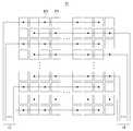
도 1은 터치 스크린이 적용된 종래 기술에 따른 터치 디스플레이 장치를 나타내는 도면이다. 도 1(A)는 애드온 방식(add on type)의 터치 디스플레이 장치를 나타내고 있고, 도 1(B)는 모디파이드 애드온 방식(Modified add on type)의 터치 디스플레이 장치를 나타내고 있고, 도 1(C)는 하이브리드 방식(hybrid type)의 터치 디스플레이 장치를 나타내고 있다.1 is a view illustrating a conventional touch display device to which a touch screen is applied. 1 (A) shows a touch display device of an add-on type (add on type), FIG. 1 (B) shows a modified add on type touch display device, A hybrid type touch display device is shown.
도 1(A)의 애드온 방식 및 도 1(B)의 모디파이드 애드온 방식의 터치 디스플레이 장치는 TFT(Thin Film Transistor) 어레이 기판(1)과 컬러필터 어레이 기판(2)을 포함하는 액정 패널 상부에 터치 스크린이 배치되어 있다. 터치 스크린에는 터치 구동전극(TX)과 터치 수신전극(RX)이 배열되어 있다. 이때, 터치 구동전극(TX)과 터치 수신전극(RX)이 서로 다른 층(layer)에 배치될 수도 있고, 서로 다른 층(layer)에 배치될 수도 있다.The add-on method of FIG. 1A and the modified display device of the modified add-on method of FIG. 1B are provided on a liquid crystal panel including a TFT (Thin Film Transistor)
도 1(C)의 하이브리드 박식의 터치 디스플레이 장치는 TFT 어레이 기판(1) 상에 터치 구동전극(TX)이 배치되고, 컬러필터 어레이 기판(2) 상에 터치 수신전극(RX)이 배치되어 있다.1 (C), a touch-driven electrode TX is disposed on a
이러한, 종래 기술에 따른 터치 디스플레이 장치는 액정 패널과 터치 스크린을 별도로 제조해야 함으로, 제조 공정이 복잡하고 비용이 증가하는 문제점 있다.Such a conventional touch display device requires a liquid crystal panel and a touch screen separately, which complicates the manufacturing process and increases the cost.
최근에 들어 터치 디스플레이 장치의 두께를 줄고 제조 비용을 절감시키기 위해서 터치 전극(터치 센서)를 액정 패널의 셀 내부에 내장시키는 인 셀 터치(in cell touch) 액정 디스플레이 장치가 개발되었다. 인셀 터치 액정 디스플레이 장치는 액정 패널의 TFT 어레이 기판에 배치된 공통 전극을 터치 센서로 이용한다. In recent years, an in-cell touch liquid crystal display device has been developed in which a touch electrode (touch sensor) is embedded in a cell of a liquid crystal panel in order to reduce the thickness of the touch display device and reduce the manufacturing cost. The Insel-Touch liquid crystal display device uses a common electrode disposed on a TFT array substrate of a liquid crystal panel as a touch sensor.
도 2는 뮤추얼 정전용량 방식(mutual capacitive type)의 인셀 터치 액정 디스플레이 장치를 나타내는 도면이다.2 is a view showing an in-cell touch liquid crystal display device of a mutual capacitive type.
도 2를 참조하면, 뮤추얼 정전용량 방식의 인셀 터치 액정 디스플레이 장치는 액정 패널(10)의 TFT 어레이 기판에 배열된 공통 전극을 터치 구동전극(TX)과 터치 수신전극(RX)으로 구동시킨다. 이러한, 뮤추얼 정전용량 방식은 터치 구동라인(14)과 터치 수신라인(12)을 액정 패널(10)의 좌측 및 우측 베젤(bezel) 영역에 배치함으로 인해서 베젤 폭이 증가하는 문제점이 있다.Referring to FIG. 2, the mutual capacitance type Insel-Touch liquid crystal display device drives a common electrode arranged on the TFT array substrate of the
도 3은 공통 전극 탑(Vcom top) 방식의 인셀 터치 디스플레이 장치의 제조공정을 개략적으로 나타내는 것으로, 제조공정에 소요되는 마스크의 개수를 나타내고 있다.3 schematically shows a manufacturing process of a common electrode top (Vcom top) type in-cell touch display device, and shows the number of masks required for the manufacturing process.
도 3을 참조하면, 종래 기술에 따른 인셀 터치 액정 디스플레이 장치는 픽셀의 구조에서 공통 전극이 최상층에 위치하고, 공통 전극의 아래에 픽셀 전극이 배치된 공통 전극 탑(Vcom top) 픽셀 구조를 적용하고 있다.Referring to FIG. 3, the conventional in-cell touch-type liquid crystal display device employs a common pixel top (Vcom top) pixel structure in which a common electrode is located on the uppermost layer and a pixel electrode is disposed below the common electrode .
TFT의 액티브층의 재료로 저온 다결정 실리콘(LTPS: Low Temperature Poly Silicon)이 이용되고, 공통 전극 탑(Vcom top) 픽셀 구조가 적용된 종래 기술에 따른 인셀 터치 액정 디스플레이 장치는 제조 공정에 11개의 마스크가 소요되고, 이에 따른 다수의 세부공정을 수행하게 된다. 이로 인해, 제조 공정이 복잡하고 제조 비용이 증가하는 문제점이 있다.Conventional Insel Touch Liquid Crystal Display devices using low temperature polysilicon (LTPS) as a material of an active layer of a TFT and applying a common electrode top (Vcom top) pixel structure have eleven masks And a number of detailed processes are performed accordingly. As a result, the manufacturing process is complicated and the manufacturing cost is increased.
또한, 공통 전극 탑(Vcom top) 픽셀 구조를 적용하면, 픽셀들의 경계 부분에서의 광 투과율이 높아 레드, 그린 및 블루 픽셀들 간의 혼색이 발생하는 문제점이 있다.Further, when the common electrode top (Vcom top) pixel structure is applied, there is a problem that the light transmittance at the boundary portion of the pixels is high, resulting in color mixture between red, green and blue pixels.
본 발명은 상술한 문제점을 해결하기 위한 것으로서, 픽셀 전극 탑(pixel electrode top) 구조의 인셀 터치 액정 디스플레이 장치와 이의 제조방법을 제공하는 것을 기술적 과제로 한다.SUMMARY OF THE INVENTION The present invention has been made to solve the above-mentioned problems, and it is an object of the present invention to provide an Insel-Touch liquid crystal display device having a pixel electrode top structure and a method of manufacturing the same.
본 발명은 상술한 문제점을 해결하기 위한 것으로서, 픽셀들 간의 혼색을 방지할 수 있는 인셀 터치 액정 디스플레이 장치와 이의 제조방법을 제공하는 것을 기술적 과제로 한다.Disclosure of Invention Technical Problem [8] Accordingly, the present invention has been made in view of the above problems, and it is an object of the present invention to provide an in-cell touch-sensitive liquid crystal display device and a method of manufacturing the same, which can prevent color mixing between pixels.
본 발명은 상술한 문제점을 해결하기 위한 것으로서, 인셀 터치 액정 디스플레이 장치의 제조에 소요되는 마스크의 개수 및 제조 공정을 줄이는 것을 기술적 과제로 한다.SUMMARY OF THE INVENTION The present invention has been made in view of the above problems, and it is a technical object of the present invention to reduce the number of masks and the manufacturing process required for manufacturing the Insel-Touch liquid crystal display device.
본 발명은 상술한 문제점을 해결하기 위한 것으로서, 터치 디스플레이 장치의 제조에 소요되는 비용을 줄이는 것을 기술적 과제로 한다.SUMMARY OF THE INVENTION The present invention has been made to solve the above problems and it is a technical object of the present invention to reduce the manufacturing cost of a touch display device.
위에서 언급된 본 발명의 기술적 과제 외에도, 본 발명의 다른 특징 및 이점들이 이하에서 기술되거나, 그러한 기술 및 설명으로부터 본 발명이 속하는 기술분야에서 통상의 지식을 가진 자에게 명확하게 이해될 수 있을 것이다.Other features and advantages of the invention will be set forth in the description which follows, or may be obvious to those skilled in the art from the description and the claims.
본 발명의 실시 예에 따른 인셀 터치 액정 디스플레이 장치는 복수의 픽셀 영역에 TFT(thin film transistor)가 배치되어 있다. 상기 TFT의 소스 전극과 접속된 소스 컨택부 및 드레인 전극과 접속된 드레인 컨택부가 배치되어 있다. 상기 소스 컨택부 및 드레인 컨택부 상에 제1 보호층 및 제2 보호층이 배치되어 있다. 상기 제2 보호층 상에 공통 전극이 배치되어 있고, 상기 공통 전극 상에 제3 보호층이 배치되어 있다. 상기 제3 보호층을 관통하여 상기 공통 전극과 중첩되도록 전도성 라인이 배치되어 있다. 그리고, 픽셀 전극이 제1 컨택홀에서 상기 드레인 컨택부와 접속되고, 상기 제3 보호층 상에 배치되어 있다.In an Insel-Touch liquid crystal display device according to an embodiment of the present invention, a thin film transistor (TFT) is disposed in a plurality of pixel regions. A source contact portion connected to the source electrode of the TFT, and a drain contact portion connected to the drain electrode. A first passivation layer and a second passivation layer are disposed on the source contact portion and the drain contact portion. A common electrode is disposed on the second protective layer, and a third protective layer is disposed on the common electrode. And a conductive line extending through the third passivation layer and overlapping the common electrode. A pixel electrode is connected to the drain contact portion in the first contact hole, and is disposed on the third passivation layer.
본 발명의 실시 예에 따른 인셀 터치 액정 디스플레이 장치의 제조방법은 복수의 픽셀 영역에 TFT(thin film transistor)를 형성한다. 상기 TFT의 소스 전극과 접속되는 소스 컨택부 및 드레인 전극과 접속되는 드레인 컨택부를 형성한다. 상기 소스 컨택부 및 드레인 컨택부 상에 제1 보호층 및 제2 보호층을 형성한다. 상기 제2 보호층 상에 공통 전극을 형성하고, 상기 공통 전극 상에 제3 보호층을 형성한다. 상기 드레인 컨택부를 노출시키는 제1 컨택홀 및 상기 공통 전극의 일부를 노출시키는 제2 컨택홀을 형성한다. 상기 공통 전극과 접속되도록 전도성 라인을 형성한다. 상기 제1 컨택홀 내부 및 상기 제3 보호층 상에 픽셀 전극을 형성한다.A method of manufacturing an in-cell touch-sensitive liquid crystal display device according to an embodiment of the present invention includes forming a thin film transistor (TFT) on a plurality of pixel regions. A source contact portion connected to the source electrode of the TFT and a drain contact portion connected to the drain electrode are formed. A first passivation layer and a second passivation layer are formed on the source contact portion and the drain contact portion. A common electrode is formed on the second protective layer, and a third protective layer is formed on the common electrode. A first contact hole exposing the drain contact portion and a second contact hole exposing a part of the common electrode are formed. And a conductive line is formed so as to be connected to the common electrode. A pixel electrode is formed in the first contact hole and on the third passivation layer.
본 발명은 픽셀 전극 탑(pixel electrode top) 구조의 인셀 터치 액정 디스플레이 장치와 이의 제조방법을 제공할 수 있다.The present invention can provide an Insel-Touch liquid crystal display device having a pixel electrode top structure and a method of manufacturing the same.
본 발명의 실시 예에 따른 인셀 터치 액정 디스플레이 장치는 픽셀 전극 탑(pixel electrode top) 구조로 형성되어 픽셀들 간의 혼색을 방지할 수 있다.The in-cell touch-sensitive liquid crystal display device according to the embodiment of the present invention may have a pixel electrode top structure to prevent color mixture between pixels.
본 발명의 실시 예에 따른 인셀 터치 액정 디스플레이 장치는 공통 전극과 전도성 라인이 직접 접촉(direct contact)되어 있어, 공통 전극과 전도성 라인을 접촉시키는 구조를 형성함으로 인해 발생하는 픽셀의 개구율 손실을 줄일 수 있다.The Insel-Touch liquid crystal display device according to an embodiment of the present invention has a structure in which a common electrode and a conductive line are in direct contact with each other, thereby forming a structure in which a common electrode and a conductive line are in contact with each other. have.
본 발명의 실시 예에 따른 인셀 터치 액정 디스플레이 장치의 제조방법은 인셀 터치 액정 디스플레이 장치의 제조에 소요되는 마스크의 개수 및 제조 공정을 줄일 수 있다.The method of manufacturing the in-cell touch-sensitive liquid crystal display device according to the embodiment of the present invention can reduce the number of masks and manufacturing process required for manufacturing the in-cell touch-sensitive liquid crystal display device.
본 발명의 실시 예에 따른 인셀 터치 액정 디스플레이 장치의 제조방법은 인셀 터치 액정 디스플레이 장치의 제조에 소요되는 비용을 줄일 수 있다.The manufacturing method of the in-line touch-type liquid crystal display device according to the embodiment of the present invention can reduce the manufacturing cost of the in-line touch-type liquid crystal display device.
이 밖에도, 본 발명의 실시 예들을 통해 본 발명의 또 다른 특징 및 이점들이 새롭게 파악될 수도 있을 것이다.In addition, other features and advantages of the present invention may be newly understood through embodiments of the present invention.
도 1은 터치 스크린이 적용된 종래 기술에 따른 터치 디스플레이 장치를 나타내는 도면이다.
도 2는 뮤추얼 정전용량 방식(mutual capacitive type)의 인셀 터치 액정 디스플레이 장치를 나타내는 도면이다.
도 3은 공통 전극 탑(Vcom top) 방식의 인셀 터치 디스플레이 장치의 제조공정을 개략적으로 나타내는 것으로, 제조공정에 소요되는 마스크의 개수를 나타내고 있다.
도 4는 본 발명의 실시 예에 따른 인셀 터치 액정 디스플레이 장치를 나타내는 것으로, TFT 어레이 기판에 배치된 픽셀의 단면 구조를 나타내고 있다.
도 5는 본 발명의 실시 예에 따른 인셀 터치 액정 디스플레이 장치의 제조방법을 개략적으로 나타내는 것으로, 제조공정에 소요되는 마스크의 개수를 나타내고 있다.
도 6 내지 도 15는 본 발명의 실시 예에 따른 인셀 터치 액정 디스플레이 장치의 제조방법을 나타내는 도면이다.
도 16은 터치 전극과 드라이브 IC(integrated circuit)을 연결시키는 전도성 라인의 배열 구조의 일 예를 나타내는 도면이다.
도 17은 터치 전극과 드라이브 IC(integrated circuit)을 연결시키는 전도성 라인의 배열 구조의 다른 예를 나타내는 도면이다.1 is a view illustrating a conventional touch display device to which a touch screen is applied.
2 is a view showing an in-cell touch liquid crystal display device of a mutual capacitive type.
3 schematically shows a manufacturing process of an in-line touch display device of a common electrode top (Vcom top) type, and shows the number of masks required for the manufacturing process.
FIG. 4 illustrates a cross-sectional structure of a pixel arranged on a TFT array substrate, according to an embodiment of the present invention.
5 schematically shows a method of manufacturing an in-cell touch-sensitive liquid crystal display device according to an embodiment of the present invention, and shows the number of masks required for the manufacturing process.
6 to 15 are views illustrating a method of manufacturing an in-cell touch-sensitive liquid crystal display device according to an embodiment of the present invention.
16 is a diagram showing an example of the arrangement structure of conductive lines connecting a touch electrode and a drive IC (integrated circuit).
17 is a view showing another example of the arrangement structure of the conductive lines connecting the touch electrode and the drive IC (integrated circuit).
명세서 전체에 걸쳐서 동일한 참조번호들은 실질적으로 동일한 구성요소들을 의미한다. 이하의 설명에서, 본 발명의 핵심 구성과 관련이 없는 경우 및 본 발명의 기술분야에 공지된 구성과 기능에 대한 상세한 설명은 생략될 수 있다.Like reference numerals throughout the specification denote substantially identical components. In the following description, detailed descriptions of configurations and functions known in the technical field of the present invention and those not related to the core configuration of the present invention can be omitted.
본 발명의 이점 및 특징, 그리고 그것들을 달성하는 방법은 첨부되는 도면과 함께 상세하게 후술되어 있는 실시 예들을 참조하면 명확해질 것이다. 그러나 본 발명은 이하에서 개시되는 실시 예들에 한정되는 것이 아니라 서로 다른 다양한 형태로 구현될 것이며, 단지 본 실시 예들은 본 발명의 개시가 완전하도록 하며, 본 발명이 속하는 기술 분야에서 통상의 지식을 가진 자에게 발명의 범주를 완전하게 알려주기 위해 제공되는 것이며, 본 발명은 청구항의 범주에 의해 정의될 뿐이다.BRIEF DESCRIPTION OF THE DRAWINGS The advantages and features of the present invention and the manner of achieving them will become apparent with reference to the embodiments described in detail below with reference to the accompanying drawings. The present invention may, however, be embodied in many different forms and should not be construed as being limited to the embodiments set forth herein. Rather, these embodiments are provided so that this disclosure will be thorough and complete, and will fully convey the concept of the invention to those skilled in the art. To fully disclose the scope of the invention to a person skilled in the art, and the invention is only defined by the scope of the claims.
본 명세서에서 각 도면의 구성요소들에 참조번호를 부가함에 있어서 동일한 구성 요소들에 한해서는 비록 다른 도면상에 표시되더라도 가능한 한 동일한 번호를 가지도록 하고 있음에 유의하여야 한다.It should be noted that, in the specification of the present invention, the same reference numerals as in the drawings denote the same elements, but they are numbered as much as possible even if they are shown in different drawings.
본 발명의 실시 예를 설명하기 위한 도면에 개시된 형상, 크기, 비율, 각도, 개수 등은 예시적인 것이므로 본 발명이 도시된 사항에 한정되는 것은 아니다. 명세서 전체에 걸쳐 동일 참조 부호는 동일 구성 요소를 지칭한다. 또한, 본 발명을 설명함에 있어서, 관련된 공지 기술에 대한 구체적인 설명이 본 발명의 요지를 불필요하게 흐릴 수 있다고 판단되는 경우 그 상세한 설명은 생략한다. 본 명세서 상에서 언급한 '포함한다', '갖는다', '이루어진다' 등이 사용되는 경우 '~만'이 사용되지 않는 이상 다른 부분이 추가될 수 있다. 구성 요소를 단수로 표현한 경우에 특별히 명시적인 기재 사항이 없는 한 복수를 포함하는 경우를 포함한다.The shapes, sizes, ratios, angles, numbers, and the like disclosed in the drawings for describing the embodiments of the present invention are illustrative, and thus the present invention is not limited thereto. Like reference numerals refer to like elements throughout the specification. In the following description, well-known functions or constructions are not described in detail since they would obscure the invention in unnecessary detail. In the case where the word 'includes', 'having', 'done', etc. are used in this specification, other parts can be added unless '~ only' is used. Unless the context clearly dictates otherwise, including the plural unless the context clearly dictates otherwise.
구성 요소를 해석함에 있어서, 별도의 명시적 기재가 없더라도 오차 범위를 포함하는 것으로 해석한다.In interpreting the constituent elements, it is construed to include the error range even if there is no separate description.
위치 관계에 대한 설명일 경우, 예를 들어, '~상에', '~상부에', '~하부에', '~옆에' 등으로 두 부분의 위치 관계가 설명되는 경우, '바로' 또는 '직접'이 사용되지 않는 이상 두 부분 사이에 하나 이상의 다른 부분이 위치할 수도 있다.In the case of a description of the positional relationship, for example, if the positional relationship between two parts is described as 'on', 'on top', 'under', and 'next to' Or " direct " is not used, one or more other portions may be located between the two portions.
시간 관계에 대한 설명일 경우, 예를 들어, '~후에', '~에 이어서', '~다음에', '~전에' 등으로 시간적 선후 관계가 설명되는 경우, '바로' 또는 '직접'이 사용되지 않는 이상 연속적이지 않은 경우도 포함할 수 있다.In the case of a description of a temporal relationship, for example, if the temporal relationship is described by 'after', 'after', 'after', 'before', etc., May not be continuous unless they are not used.
'적어도 하나'의 용어는 하나 이상의 관련 항목으로부터 제시 가능한 모든 조합을 포함하는 것으로 이해되어야 한다. 예를 들어, '제1 항목, 제 2 항목 및 제 3 항목 중에서 적어도 하나'의 의미는 제1 항목, 제 2 항목 또는 제 3 항목 각각 뿐만 아니라 제1 항목, 제 2 항목 및 제 3 항목 중에서 2개 이상으로부터 제시될 수 있는 모든 항목의 조합을 의미한다.The term " at least one " should be understood to include all possible combinations from one or more related items. For example, the meaning of 'at least one of the first item, the second item and the third item' means not only the first item, the second item or the third item, but also the second item, the second item and the third item, Means any combination of items that can be presented from more than one.
제1, 제2 등이 다양한 구성요소들을 서술하기 위해서 사용되나, 이들 구성요소들은 이들 용어에 의해 제한되지 않는다. 이들 용어들은 단지 하나의 구성 요소를 다른 구성요소와 구별하기 위하여 사용하는 것이다. 따라서, 이하에서 언급되는 제1 구성요소는 본 발명의 기술적 사상 내에서 제2 구성요소일 수도 있다.The first, second, etc. are used to describe various components, but these components are not limited by these terms. These terms are used only to distinguish one component from another. Therefore, the first component mentioned below may be the second component within the technical spirit of the present invention.
본 발명의 여러 실시 예들의 각각 특징들이 부분적으로 또는 전체적으로 서로 결합 또는 조합 가능하고, 기술적으로 다양한 연동 및 구동이 가능하며, 각 실시 예들이 서로에 대하여 독립적으로 실시 가능할 수도 있고 연관 관계로 함께 실시할 수도 있다.It is to be understood that each of the features of the various embodiments of the present invention may be combined or combined with each other, partially or wholly, technically various interlocking and driving, and that the embodiments may be practiced independently of each other, It is possible.
액정 디스플레이 장치는 액정층의 배열을 조절하는 방식에 따라 TN(Twisted Nematic) 모드, VA(Vertical Alignment) 모드, IPS(In Plane Switching) 모드, FFS(Fringe Field Switching) 모드 등 다양하게 개발되어 있다.The liquid crystal display device has been developed in various ways such as TN (Twisted Nematic) mode, VA (Vertical Alignment) mode, IPS (In Plane Switching) mode and FFS (Fringe Field Switching) mode according to a method of adjusting the arrangement of liquid crystal layers.
그 중에서, IPS 모드와 FFS 모드는 하부 기판 상에 픽셀 전극과 공통 전극을 배치하여 픽셀 전극과 공통 전극 사이의 전계에 의해 액정층의 배열을 조절하는 방식이다.In the IPS mode and the FFS mode, a pixel electrode and a common electrode are disposed on a lower substrate to adjust the alignment of the liquid crystal layer by an electric field between the pixel electrode and the common electrode.
특히, IPS 모드는 픽셀 전극과 공통 전극을 평행하게 교대로 배열함으로써 양 전극 사이에서 횡전계를 일으켜 액정층의 배열을 조절하는 방식이다. 이와 같은 IPS 모드는 픽셀 전극과 공통 전극 상측 부분에서 액정층의 배열이 조절되지 않아 그 영역에서 광의 투과도가 저하되는 단점이 있다.In particular, in the IPS mode, a pixel electrode and a common electrode are alternately arranged in parallel so that a horizontal electric field is generated between both electrodes to adjust the alignment of the liquid crystal layer. In such an IPS mode, the alignment of the liquid crystal layer is not controlled in the upper portion of the pixel electrode and the common electrode, so that the transmittance of light is reduced in the region.
이와 같은 IPS 모드의 단점을 해결하기 위해 고안된 것이 FFS 모드이다. FFS 모드는 상기 픽셀 전극과 상기 공통 전극을 절연층을 사이에 두고 이격되도록 형성시킨다.The FFS mode is designed to overcome the shortcomings of the IPS mode. In the FFS mode, the pixel electrode and the common electrode are spaced apart with an insulating layer therebetween.
하나의 전극은 판(plate) 형상 또는 패턴 형상으로 구성하고 다른 하나의 전극은 핑거(finger) 형상으로 구성하여 양 전극 사이에서 발생되는 프린지 필드(Fringe Field)를 통해 액정층의 배열을 조절하는 방식이다.One electrode may be formed in a plate shape or a pattern shape and the other electrode may be formed in a finger shape to adjust the alignment of the liquid crystal layer through a fringe field generated between the electrodes to be.
본 발명의 실시 예에 따른 인셀 터치 액정 디스플레이 장치와 이의 제조방법은 FFS 모드의 TFT(Thin Film Transistor) 어레이 기판(하부 기판) 및 이의 제조를 위한 것으로, 사용자의 터치를 검출하는 터치 센서를 TFT 어레이 기판(하부 기판)에 내장하였다.The Insel-Touch liquid crystal display device and the method of manufacturing the same according to the embodiment of the present invention are for fabricating an FFS mode TFT (Thin Film Transistor) array substrate (lower substrate) (Lower substrate).
TFT 어레이 기판에는 복수의 픽셀이 형성되며, 상기 복수의 픽셀 각각은 서로 교차하는 데이터 라인들(미도시)과 게이트 라인들(미도시)에 의해 정의된다. 상기 데이터 라인들과 상기 게이트 라인들이 교차되는 영역 마다 픽셀이 정의되고, 각 픽셀에는 TFT가 배치되어 있다.A plurality of pixels are formed on the TFT array substrate, and each of the plurality of pixels is defined by data lines (not shown) and gate lines (not shown) which intersect with each other. A pixel is defined for each region where the data lines and the gate lines intersect, and a TFT is disposed for each pixel.
이하, 도면을 참조하여 본 발명의 실시 예에 따른 인셀 터치 액정 디스플레이 장치와 이의 제조방법에 대해서 설명하기로 한다.Hereinafter, an in-cell touch-sensitive liquid crystal display device and a method of manufacturing the same will be described with reference to the drawings.
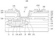
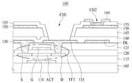
도 4는 본 발명의 실시 예에 따른 인셀 터치 액정 디스플레이 장치를 나타내는 것으로, TFT 어레이 기판에 배치된 픽셀의 단면 구조를 나타내고 있다. 도 4에는 FFS(Fringe Field Switch) 모드의 TFT 어레이 기판(하부 기판) 구조를 나타내고 있으며, 복수의 픽셀 중에서 하나의 픽셀 구조를 도시하고 있다. 도 4에서는 인셀 터치 타입으로 터치 센서가 TFT 어레이 기판에 내재화 된 것을 도시하고 있다. 도 4에서는 픽셀 전극 탑(pixel electrode top) 픽셀 구조를 도시하고 있다.FIG. 4 illustrates a cross-sectional structure of a pixel arranged on a TFT array substrate, according to an embodiment of the present invention. FIG. 4 shows a structure of a TFT array substrate (lower substrate) in an FFS (Fringe Field Switch) mode, and shows one pixel structure among a plurality of pixels. 4 shows that the touch sensor is internalized on the TFT array substrate by the in-cell touch type. FIG. 4 shows a pixel electrode top pixel structure.
도 4에서는 컬러필터 어레이 기판(상부 기판), 액정층, 백라이트 유닛 및 구동 회로부의 도시는 생략되었다. 구동 회로부는 타이밍 컨트롤러(T-con), 데이터 드라이버(D-IC), 게이트 드라이버(G-IC), 센싱 드라이버, 백라이트 구동부, 구동 회로들에 구동 전원을 공급하는 전원 공급부를 포함한다. 여기서, 구동 회로부의 전체 또는 일부는 COG(Chip On Glass) 또는 COF(Chip On Flexible Printed Circuit, Chip On Film) 방식으로 액정 패널 상에 형성될 수 있다.In FIG. 4, illustration of the color filter array substrate (upper substrate), the liquid crystal layer, the backlight unit, and the driving circuit are omitted. The driving circuit unit includes a power supply unit for supplying driving power to the timing controller (T-con), the data driver (D-IC), the gate driver (G-IC), the sensing driver, the backlight driver and the driving circuits. Here, all or a part of the driving circuit portion may be formed on the liquid crystal panel by COG (Chip On Glass) or COF (Chip On Flexible Printed Circuit) method.
이하, 도 4를 참조하여, 본 발명의 실시 예에 따른 인셀 터치 액정 디스플레이 장치에 대하여 설명한다. 도 4에서 본 발명의 실시 예에 따른 인셀 터치 액정 디스플레이 장치의 TFT 어레이 기판의 픽셀 구조를 도시하고 있다.Hereinafter, an in-cell touch-sensitive liquid crystal display device according to an embodiment of the present invention will be described with reference to FIG. 4 shows a pixel structure of a TFT array substrate of an in-cell touch-sensitive liquid crystal display device according to an embodiment of the present invention.
TFT 어레이 기판은 글래스 기판(105), 차광층(110, light shield layer), 버퍼층(115, buffer layer), 게이트 절연층(120, gate insulator), 층간 절연층(125, ILD: Inter Layer Dielectric), 소스 컨택부(130), 드레인 컨택부(135), 제1 보호층(140, PAS0), 제2 보호층(145, PAS1), 공통 전극(150, Common electrode), 제3 보호층(155, PAS2), 전도성 라인(160), 픽셀 전극(170, Pixel electrode), 게이트 전극(G), 액티브층(ACT), 소스 전극(S), 드레인 전극(D)으로 구성된 TFT(thin film transistor)를 포함한다.The TFT array substrate includes a
글래스 기판(105) 상부 중에서 TFT의 액티브층(ACT)과 대응되는 부분에 차광층(110)이 배치되어 있다. 차광층(110)은 불투명 메탈로 형성되어 있어 액티브층(ACT)에 광이 조사되는 것을 방지한다. 이러한, 차광층(110)은 몰리브덴(Mo) 또는 알루미늄(Al)으로 형성되며, 500~1,000Å의 두께를 가질 수 있다.The
차광층(110) 위에는 버퍼층(115)이 형성되어 있다. 버퍼층(115)은 SiO2, 또는 SiNx 물질로 형성되며, 2,000~3,000Å의 두께를 가질 수 있다.A
버퍼층(115) 상부 중에서 차광층(110)과 중첩되는 영역에 TFT의 액티브층(ACT), 소스 전극(S), 드레인 전극(D)이 배치되어 있다.The active layer ACT, the source electrode S, and the drain electrode D of the TFT are disposed in an area overlapping the
액티브층(ACT), 소스 전극(S), 드레인 전극(D)을 덮도록 게이트 절연층(120)이 배치되어 있다. 게이트 절연층(120)은 SiO2물질로 형성될 수 있으며, 1,000~1,500Å의 두께를 가질 수 있다.The
한편, 게이트 절연층(120)은 TEOS(Tetra Ethyl Ortho Silicate) 또는 MTO(Middle Temperature Oxide)를 CVD(Chemical Vapor Deposition)로 증착하여 형성될 수도 있다.Meanwhile, the
게이트 절연층(120)의 상부 중에서 액티브층(ACT)과 중첩되는 영역에 게이트 전극(G)이 배치되어 있다. 이때, 게이트 전극(G)은 알루미늄(Al) 또는 몰리브덴(Mo)으로 형성되며, 2,000~3,000Å의 두께를 가질 수 있다. 이와 같이, 게이트 절연층(120) 아래에 배치된 액티브층(ACT), 소스 전극(S), 드레인 전극(D)과 게이트 절연층(120) 위에 배치된 게이트 전극(G)으로 TFT가 구성된다. 여기서, TFT는 코플레너 탑 게이트(coplanar top gate) 구조로 형성되어 있다.A gate electrode G is disposed in an area overlapping the active layer ACT in the upper portion of the
게이트 절연층(120) 및 TFT를 덮도록 층간 절연층(125)이 배치되어 있다. 층간 절연층(125)은 SiO2 또는 SiNx 물질로 형성될 수 있으며, 3,000~6,000Å의 두께를 가질 수 있다. 다른 예로서, 층간 절연층(125)은 SiO2(3,000Å)/SiNx(3,000Å)가 적층된 구조로도 형성될 수도 있다.An interlayer insulating
게이트 절연층(120)과 층간 절연층(125)을 관통하여 TFT의 소스 전극(S)과 접속된 소스 컨택부(130)가 배치되어 있다. 그리고, 게이트 절연층(120)과 층간 절연층(125)을 관통하여 TFT의 드레인 전극(D)과 접속된 드레인 컨택부(135)가 배치되어 있다.A
소스 컨택부(130) 및 드레인 컨택부(135)는 몰리브덴(Mo)/알루미늄(Al)몰리브덴(Mo)이 적층된 다층(multi layer) 구조로 형성될 수 있다. 소스 컨택부(130)는 데이터 라인과 접속되고, 드레인 컨택부(135)는 픽셀 전극(170)과 접속된다.The
층간 절연층(125), 소스 컨택부(130) 및 드레인 컨택부(135)를 덮도록 제1 보호층(140, PAS0)이 배치되어 있다. 제1 보호층(140, PAS0)은 SiO2 또는 SiNx 물질로 형성되며, 1,000~2,000Å의 두께를 가진다.The
제1 보호층(140, PAS0)을 덮도록 제2 보호층(145, PAS1)이 배치되어 있다. 제2 보호층(145, PAS1)은 포토 아크릴(photo acryl)로 형성되며, 2.0~3.0um의 두께를 가진다.The second passivation layer 145 (PAS1) is disposed to cover the first passivation layer 140 (PAS0). The second passivation layer 145 (PAS1) is formed of photo acryl and has a thickness of 2.0 to 3.0 .mu.m.
제2 보호층(145, PAS1)의 상부에 공통 전극(150, Common electrode)이 배치되어 있다. 공통 전극(150)은 ITO(indium tin oxide), IZO(indium zinc oxide) 또는 ITZO(indium tin zinc oxide)와 같은 투명 전도성 물질 형성되며, 500~1,500Å의 두께를 가진다.A
공통 전극(150)을 덮도록 제3 보호층(155, PAS2)이 배치되어 있다. 제3 보호층(155, PAS2)은 SiO2, 또는 SiNx 물질로 형성되며, 2,000~3,000Å의 두께를 가질 수 있다.And the third protective layer 155 (PAS2) is disposed so as to cover the
드레인 컨택부(135)와 중첩된 부분의 제1 보호층(140, PAS0), 제2 보호층(145, PAS1) 및 제3 보호층(155, PAS2)이 제거되어 제1 컨택홀(CH1)이 형성되어 있다.The
제3 보호층(155, PAS2) 상부와 제1 컨택홀(CH1) 내부에 픽셀 전극(170)이 배치된다. 픽셀 전극(170)은 ITO(indium tin oxide), IZO(indium zinc oxide) 또는 ITZO(indium tin zinc oxide)와 같은 투명 전도성 물질 형성되며, 500~1,500Å의 두께를 가진다. 픽셀 전극(170)은 핑거(finger) 형상으로 형성되어, 공통 전극(150)과 픽셀 전극(170) 사이에 프린지 필드가 형성되게 된다.The
여기서, 제3 보호층(155, PAS2) 중에서 데이터 라인(DL) 및 공통 전극(150)과 중첩된 부분에는 제2 컨택홀(CH2)이 형성되어 있고, 제2 컨택홀(CH2) 내부 및 제3 보호층(155, PAS2) 상부에 전도성 라인(160)이 배치되어 있다. 이와 같이, 제2 컨택홀(CH2) 내에서 공통 전극(150)과 전도성 라인(160)이 직접 접촉(direct contact)되어 있다.A second contact hole CH2 is formed in a portion of the
전도성 라인(160)은 몰리브덴(Mo) 또는 알루미늄(Al)으로 형성될 수 있으며, 1,500~2,000Å의 두께를 가질 수 있다. 한편, 전도성 라인(160)은 몰리브덴(Mo)/알루미늄(Al)/ 몰리브덴(Mo)이 적층된 다층(multi layer) 구조로도 형성될 수 있다.The
여기서, 전도성 라인(160)은 데이터 라인(DL)과 중첩되도록 배치되게 되는데, 레드, 그린 및 블루 픽셀의 데이터 라인과 모두 중첩되지는 않는다. 레드 픽셀의 데이터 라인 상에 컬럼 스페이서가 배치되는 경우, 전도성 라인은 그린 픽셀의 데이터 라인 및 블루 픽셀의 데이터 라인과 중첩되도록 배치될 수 있다. 그러나, 반드시 이에 한정되는 것은 아니며, 전도성 라인(160)은 레드, 그린 및 블루 픽셀의 데이터 라인 중에서 어느 것과도 중첩되게 배치될 수 있다.Here, the
전도성 라인(160)은 복수의 픽셀에 배치된 공통 전극(150)과 전기적으로 접속되며, 액정 패널 내에서 데이터 라인의 상부에 배치된다. 전도성 라인(160)은 액정 패널에의 상부에서 하부로 바(bar) 형태로 배치된다. 전도성 라인(160)과 픽셀 전극(170)은 서로 접촉되지 않는다. 도 16 및 도 17을 참조하면, 공통 전극(150)과 접속된 전도성 라인(160) 각각은 링크 라인을 통해 드라이브 IC(190)의 채널과 접속된다.The
이러한, 전도성 라인(160)에 의해 공통 전극(150)이 터치 기간(비 표시 기간)에 터치 전극으로 기능한다. 표시 기간에는 전도성 라인(160)에 공통 전압이 공급된다. 그리고, 터치 기간(비 표시 기간)에는 전도성 라인(160)을 통해 공통 전극에 터치 구동 신호를 공급한 후, 전도성 라인(160)을 통해 공통 전극에 형성된 정전용량을 센싱하여 터치의 유무 및 유치를 검출하게 된다.By the
도 4에 도시하지는 않았지만, TFT 어레이 기판 상에는 복수의 게이트 라인 및 복수의 데이터 라인이 상호 교차하도록 형성되어 있다. 상기 복수의 게이트 라인 및 복수의 데이터 라인이 교차되는 영역에 TFT가 형성되게 된다. 그리고, 각 픽셀에는 스토리지 커패시터가 형성되어 있다.Although not shown in FIG. 4, a plurality of gate lines and a plurality of data lines cross each other on the TFT array substrate. A TFT is formed in a region where the plurality of gate lines and the plurality of data lines intersect. A storage capacitor is formed in each pixel.
종래 기술에서는 픽셀이 공통 전극 탑(Vcom top) 구조로 형성되어 있었으나, 본 발명의 실시 예에 따른 인셀 터치 액정 디스플레이 장치는 픽셀이 픽셀 전극 탑(pixel electrode top) 구조로 형성되어 있다. 이를 통해, 본 발명은 픽셀 전극 탑(pixel electrode top) 구조로 픽셀이 구성된 인셀 터치 액정 디스플레이 장치를 제공할 수 있다.In the prior art, the pixels are formed in the common electrode top (Vcom top) structure. However, in the Insel-Touch liquid crystal display device according to the embodiment of the present invention, pixels are formed in a pixel electrode top structure. Accordingly, the present invention can provide an in-cell touch liquid crystal display device in which pixels are formed in a pixel electrode top structure.
픽셀 전극 탑(pixel electrode top) 픽셀 구조는 픽셀 영역의 중앙 부분의 광 투과율이 높고, 데이터 라인 주변에서는 광 투과율이 낮은 특성이 있다. 따라서, 본 발명의 실시 예에 따른 인셀 터치 액정 디스플레이 장치는 데이터 라인들의 주변에서 광 투과율이 낮게 형성되어 픽셀들 간의 혼색을 방지할 수 있다.The pixel electrode top pixel structure has a high light transmittance at the central portion of the pixel region and a low light transmittance at the periphery of the data line. Accordingly, the in-cell touch-sensitive liquid crystal display device according to the embodiment of the present invention has a low light transmittance in the periphery of the data lines, thereby preventing color mixing between pixels.
또한, 본 발명의 실시 예에 따른 인셀 터치 액정 디스플레이 장치는 공통 전극과 전도성 라인이 직접 접촉(direct contact)되어 있어, 공통 전극과 전도성 라인을 접촉시키는 구조를 형성함으로 인해 발생하는 픽셀의 개구율 손실을 줄일 수 있다.Also, the Insel-Touch liquid crystal display device according to the embodiment of the present invention has a structure in which the common electrode and the conductive line are in direct contact with each other and the common electrode and the conductive line are in contact with each other, Can be reduced.
도 5는 본 발명의 실시 예에 따른 인셀 터치 액정 디스플레이 장치의 제조방법을 개략적으로 나타내는 것으로, 제조공정에 소요되는 마스크의 개수를 나타내고 있다. 본 발명의 실시 예에 따른 인셀 터치 액정 디스플레이 장치의 제조방법은 공통 전극 탑 방식 대비 픽셀 전극 탑 픽셀 구조에서 마스크의 개수를 줄일 수 있다.5 schematically shows a method of manufacturing an in-cell touch-sensitive liquid crystal display device according to an embodiment of the present invention, and shows the number of masks required for the manufacturing process. The method of manufacturing the in-cell touch-sensitive liquid crystal display device according to the embodiment of the present invention can reduce the number of masks in the pixel electrode top pixel structure compared to the common electrode top method.
도 5에 도시된 바와 같이, 10개의 마스크를 이용한 제조 공정을 통해 본 발명의 실시 예에 따른 인셀 터치 액정 디스플레이 장치를 제조 할 수 있다. 이하, 도 5와 함께 도 6 내지 도 15를 결부하여 본 발명의 실시 예에 따른 인셀 터치 액정 디스플레이 장치의 제조방법을 설명하기로 한다.As shown in FIG. 5, an in-cell touch-sensitive liquid crystal display device according to an embodiment of the present invention can be manufactured through a manufacturing process using ten masks. Hereinafter, a method of manufacturing an in-cell touch-sensitive liquid crystal display device according to an embodiment of the present invention will be described with reference to FIG. 5 and FIGS. 6 to 15. FIG.
도 6 내지 도 15는 본 발명의 실시 예에 따른 인셀 터치 액정 디스플레이 장치의 제조방법을 나타내는 도면이다.6 to 15 are views illustrating a method of manufacturing an in-cell touch-sensitive liquid crystal display device according to an embodiment of the present invention.
도 6을 참조하면, 글래스 기판(105) 상에 몰리브덴(Mo)과 같이 광을 차단하는 금속 물질을 도포하여 금속층을 형성한다.Referring to FIG. 6, a metal layer is formed on a
이후, 제1 마스크를 이용한 포토리소그래피(photolithography) 및 습식 에칭(etching, 식각) 공정을 통해 상기 금속층을 패터닝하여 TFT 영역에 차광층(120, light shield)을 형성한다. 이때, 차광층(110, light shield layer)은 500~1,000Å의 두께로 형성되며, 후속 공정에서 형성되는 TFT의 액티브층(ACT)과 얼라인 되도록 형성된다.Then, the metal layer is patterned through photolithography and wet etching using a first mask to form a
도 6에서는 TFT 어레이 기판의 베이스로 글래스 기판(105)이 적용된 것을 일 예로 나타내고 있으나, 플라스틱 기판이 글래스 기판(105)을 대체할 수도 있다.6 shows an example in which the
이어서, 도 7을 참조하면, 글래스 기판(105) 상부에 무기물, 일 예로서, SiO2 또는 SiNx 물질로 차광층(110, light shield layer)을 덮도록 버퍼층(115)을 형성한다. 이때, 버퍼층(115)은 2,000~3,000Å의 두께를 가질 수 있다.7, a
이후, 버퍼층(115) 상부 중에서 저온 다결정 실리콘(LTPS: Low Temperature Poly Silicon)을 증착하여 반도체층을 형성한다.Then, low temperature polysilicon (LTPS) is deposited on the
이후, 제2 마스크를 이용한 포토리소그래피 및 건식 에칭 공정을 통해 상기 반도체 레이어를 패터닝하여 차광층(110, light shield layer)과 중첩되는 영역에 TFT의 액티브층(ACT)를 형성한다. 이때, 상기 액티브층(ACT)는 500~1,500Å의 두께로 형성된다.Then, the active layer (ACT) of the TFT is formed in a region overlapping the
이어서, 도 8을 참조하면, 액티브층(ACT)를 덮도록 버퍼층(115)의 상부에 게이트 절연층(120)을 형성한다. 게이트 절연층(120)은 SiO2물질로 형성되며, 1,000~1,500Å의 두께를 가질 수 있다.Next, referring to FIG. 8, a
한편, 게이트 절연층(120)은 TEOS(Tetra Ethyl Ortho Silicate) 또는 MTO(Middle Temperature Oxide)를 CVD(Chemical Vapor Deposition)로 증착하여 형성될 수도 있다.Meanwhile, the
이후, 게이트 절연층(120)의 상부에 금속 물질을 증착시킨 후, 제3 마스크를 이용한 포토리소그래피 및 에칭 공정을 통해 상기 금속 물질을 패터닝하여 TFT의 게이트 전극(G)를 형성한다.Then, a metal material is deposited on the
이때, 게이트 전극(G)은 알루미늄(Al) 또는 몰리브덴(Mo)으로 2,000~3,000Å의 두께를 가지도록 형성될 수 있으며, 게이트 절연층(120)의 상부 중에서 액티브층(ACT)과 중첩되는 영역에 형성된다. 이러한, 게이트 전극(G)은 게이트 라인과 함께 형성된다. 이때, 게이트 라인은 액정 패널에서 제1 방향(예로서, 가로 방향)으로 배열될 수 있다.At this time, the gate electrode G may be formed of aluminum (Al) or molybdenum (Mo) to have a thickness of 2,000 to 3,000 ANGSTROM, and a region overlapping the active layer (ACT) As shown in FIG. The gate electrode G is formed together with the gate line. At this time, the gate lines may be arranged in the first direction (e.g., the horizontal direction) in the liquid crystal panel.
게이트 전극(G)를 마스크로 이용하여 액티브층(ACT)의 외곽에 P형 또는 N형의 고농도 불순물을 도핑하여 TFT의 소스 전극(S)과 드레인 전극(D)을 형성한다.A source electrode S and a drain electrode D of the TFT are formed by doping a p-type or n-type high-concentration impurity to the outside of the active layer ACT using the gate electrode G as a mask.
여기서, 게이트 전극(G)의 형성할 때, 습식 에칭 공정 및 건식 에칭 공정을 수행하게 되는데, 습식 에칭 공정과 건식 에칭 공정 사이에 상기 액티브층(ACT)에 P형 또는 N형의 불순물을 도핑할 수도 있다.Here, when forming the gate electrode G, a wet etching process and a dry etching process are performed. The active layer (ACT) is doped with a P-type or N-type impurity between the wet etching process and the dry etching process It is possible.
이와 같이, 게이트 절연층(120) 아래에 배치된 액티브층(ACT), 소스 전극(S), 드레인 전극(D)과 게이트 절연층(120) 위에 배치된 게이트 전극(G)으로 TFT가 구성된다. 여기서, TFT는 코플레너 탑 게이트(coplanar top gate) 구조로 형성되어 있다.The TFT is constituted by the active layer ACT, the source electrode S and the drain electrode D disposed below the
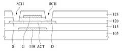
이어서, 도 9를 참조하면, TFT와 게이트 절연층(120)을 덮도록 절연물질을 증착하여 층간 절연층(125, ILD: Inter Layer Dielectric)을 형성한다. 이때, 층간 절연층(125)은 SiO2 또는 SiNx 물질로 형성되며, 3,000~6,000Å의 두께를 가질 수 있다. 다른 예로서, 층간 절연층(125)은 SiO2(3,000Å)/SiNx(3,000Å)의 구조로도 형성될 수도 있다.Referring to FIG. 9, an interlayer dielectric layer 125 (ILD) is formed by depositing an insulating material to cover the TFT and the
이후, 제4 마스크를 이용한 에칭 공정을 수행하여 TFT의 소스 전극(S)과 중첩된 부분의 게이트 절연층(120) 및 층간 절연층(125)을 제거한다. 이를 통해, TFT의 소스 전극(S)을 노출시키는 소스 컨택홀(SCH)을 형성한다. 이와 함께, TFT의 드레인 전극(D)과 중첩된 부분의 게이트 절연층(120) 및 층간 절연층(125)을 제거한다. 이를 통해, TFT의 드레인 전극(D)을 노출시키는 드레인 컨택홀(DCH)을 형성한다.Thereafter, an etching process using a fourth mask is performed to remove the
이어서, 도 10을 참조하면, 층간 절연층(125) 상에 금속 물질을 도포하여 금속층을 형성한다.Next, referring to FIG. 10, a metal layer is formed on the
이후, 제5 마스크를 이용한 포토리소그래피 및 에칭 공정을 통해 상기 금속층을 패터닝하여 복수의 픽셀에 데이터 전압을 공급하는 복수의 데이터 라인(DL)을 형성한다. 이와 함께, 상기 소스 컨택홀(SCH) 및 드레인 컨택홀(DCH)에 금속 물질을 매립하여 소스 컨택부(130) 및 드레인 컨택부(135)를 형성한다. 즉, 데이터 라인과 소스 컨택부(130) 및 드레인 컨택부(135)는 동일 마스크 공정으로 형성된다. 이때, 데이터 라인(DL)은 액정 패널에서 제2 방향(예로서, 세로 방향)으로 배열될 수 있다.Then, the metal layer is patterned through a photolithography and an etching process using a fifth mask to form a plurality of data lines DL for supplying data voltages to a plurality of pixels. At the same time, the source contact portion (SCH) and the drain contact hole (DCH) are filled with a metal material to form the
데이터 라인(DL), 소스 컨택부(130) 및 드레인 컨택부(135)는 알루미늄(Al) 또는 몰리브덴(Mo)으로 형성되며, 2,000~3,000Å의 두께를 가진다.The data line DL, the
이어서, 도 11을 참조하면, 층간 절연층(125) 상에 제1 보호층(140, PAS0)을 형성한다. 제1 보호층(140)은 층간 절연층(125), 소스 컨택부(130) 및 드레인 컨택부(135)를 덮도록 배치된다. 제1 보호층(140, PAS0)은 SiO2 또는 SiNx 물질로 형성되며, 1,000~2,000Å의 두께를 가진다.Referring to FIG. 11, a first passivation layer 140 (PAS0) is formed on the
이후, 제6 마스크를 이용한 공정을 수행하여 제1 보호층(140, PAS0)을 덮도록 제2 보호층(145, PAS1)을 형성한다. 제2 보호층(145, PAS1)은 포토 아크릴(photo acryl)로 형성되며, 2.0~3.0um의 두께를 가진다.Then, a process using a sixth mask is performed to form a second passivation layer 145 (PAS1) to cover the first passivation layer 140 (PAS0). The second passivation layer 145 (PAS1) is formed of photo acryl and has a thickness of 2.0 to 3.0 .mu.m.
드레인 컨택부(135)와 중첩되는 부분에는 제2 보호층(145, PAS1)이 형성하지 않는다. 후속 공정에서 제2 보호층(145, PAS1)이 형성되지 않은 부분에 드레인 컨택부(135)와 픽셀 전극이 컨택되는 제1 컨택홀(CH1)이 형성되게 된다. 이때, 제1 보호층(140, PAS0)은 제거하지 않고 그대로 잔존시킨다.And the second protective layer 145 (PAS1) is not formed at a portion overlapping the
이어서, 도 12를 참조하면, 제2 보호층(145, PAS1)의 상에 투명 전도성 물질을 도포한다. 이후, 제7 마스크를 이용한 포토리소그래피 및 에칭 공정을 수행하여 제2 보호층(145, PAS1)의 상부에 공통 전극(150, Common electrode)을 형성한다.Next, referring to FIG. 12, a transparent conductive material is applied on the second passivation layer 145 (PAS1). Then, a
여기서, 공통 전극(150)은 ITO(indium tin oxide), IZO(indium zinc oxide) 또는 ITZO(indium tin zinc oxide)와 같은 투명 전도성 물질로 형성되며, 500~1,500Å의 두께를 가진다.Here, the
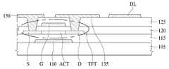
이어서, 도 13을 참조하면, 공통 전극(150)을 덮도록 제3 보호층(155)을 형성한다. 제3 보호층(155, PAS2)은 SiO2, 또는 SiNx 물질로 형성되며, 2,000~3,000Å의 두께를 가질 수 있다.Next, referring to FIG. 13, a
제8 마스크를 이용한 포토리소그래피 및 에칭 공정을 수행하여 드레인 컨택부(135)와 중첩된 부분의 제1 보호층(140, PAS0) 및 제3 보호층(155, PAS2)을 제거한다. 이를 통해, 드레인 컨택부(135)를 노출시키는 제1 컨택홀(CH1)을 형성한다.The
이와 함께, 상기 제8 마스크를 이용한 포토리소그래피 및 에칭 공정을 통해, 공통 전극(150)과 중첩된 부분의 제3 보호층(155, PAS2)을 제거한다. 이를 통해, 공통 전극(150)의 일부를 노출시키는 제2 컨택홀(CH2)을 형성한다. 제2 컨택홀(CH2)은 데이터 라인(DL) 및 공통 전극(150)과 중첩된 영역에 형성된다. 이와 같이, 제8 마스크를 이용한 포토리소그래피 및 에칭 공정을 통해 제1 컨택홀(CH1) 및 제2 컨택홀(CH2)을 한번에 형성한다.In addition, the third passivation layer 155 (PAS2) overlapped with the
여기서, 제1 컨택홀(CH1)은 TFT의 드레인 전극(D)과 픽셀 전극을 전기적으로 접속시키기 위한 것이다. 그리고, 제2 컨택홀(CH2)은 공통 전극(150)과 전도성 라인(160)을 전기적으로 접속시키기 위한 것이다.Here, the first contact hole CH1 is for electrically connecting the drain electrode D of the TFT to the pixel electrode. The second contact hole CH2 is for electrically connecting the
이어서, 도 14를 참조하면, 제3 보호층(155) 상부에 금속 물질을 도포한다. 이후, 제9 마스크를 이용한 포토리소그래피 및 에칭 공정을 수행하여 상기 금속 물질을 패터닝 한다. 이를 통해, 공통 전극(150)과 접촉하도록 전도성 라인(160)을 형성한다.Next, referring to FIG. 14, a metal material is applied on the third
제2 컨택홀(CH2) 내부 및 제3 보호층(155, PAS2) 상부에 전도성 라인(160)이 배치되고, 제2 컨택홀(CH2) 내에서 공통 전극(150)과 전도성 라인(160)이 직접 접촉(direct contact)된다.A
전도성 라인(160)은 몰리브덴(Mo) 또는 알루미늄(Al)으로 형성될 수 있으며, 1,500~2,000Å의 두께를 가질 수 있다. 한편, 전도성 라인(160)은 몰리브덴(Mo)/알루미늄(Al)/ 몰리브덴(Mo)이 적층된 다층(multi layer) 구조로도 형성될 수 있다.The
여기서, 전도성 라인(160)은 데이터 라인(DL)과 중첩되도록 형성되며, 액정 패널 내에서 세로 방향으로 인접한 픽셀들의 공통 전극(150)을 연결시킨다. 전도성 라인(160)이 레드, 그린 및 블루 픽셀의 데이터 라인과 모두 중첩되지는 않는다. 레드 픽셀의 데이터 라인 상에 컬럼 스페이서가 배치되는 경우, 전도성 라인은 그린 픽셀의 데이터 라인 및 블루 픽셀의 데이터 라인과 중첩되도록 배치될 수 있다. 그러나, 반드시 이에 한정되는 것은 아니며, 전도성 라인(160)은 레드, 그린 및 블루 픽셀의 데이터 라인 중에서 어느 것과도 중첩되게 배치될 수 있다.Here, the
이어서, 도 15를 참조하면, 제3 보호층(155, PAS2) 상부와 제1 컨택홀(CH1) 내부에 투명 전도성 물질을 도포한다. 이후, 제10 마스크를 이용한 포토리소그래피 및 에칭 공정을 수행하여 제3 보호층(155, PAS2) 상부와 제1 컨택홀(CH1) 내부에 픽셀 전극(170, pixel electrode)을 형성한다. 픽셀 전극(170)은 제1 컨택홀(CH1) 내부에서 드레인 컨택부(135)와 접속되어, TFT의 드레인 전극(D)과 픽셀 전극(170)이 전기적으로 접속된다. 전도성 라인(160)과 픽셀 전극(170)은 서로 접촉되지 않는다.Referring to FIG. 15, a transparent conductive material is applied to the upper portion of the
여기서, 픽셀 전극(170)은 ITO(indium tin oxide), IZO(indium zinc oxide) 또는 ITZO(indium tin zinc oxide)와 같은 투명 전도성 물질로 형성되며, 500~1,500Å의 두께를 가진다. 픽셀 전극(170)은 핑거(finger) 형상으로 형성되어, 공통 전극(150)과 픽셀 전극(170) 사이에 프린지 필드가 형성되게 된다.Here, the
본 발명의 실시 예에 따른 인셀 터치 액정 디스플레이 장치의 제조방법은 픽셀을 픽셀 전극 탑(pixel electrode top) 구조로 형성할 수 있다. 픽셀 전극 탑(pixel electrode top) 픽셀 구조는 픽셀 영역의 중앙 부분의 광 투과율이 높고, 데이터 라인 주변에서는 광 투과율이 낮은 특성이 있다. 따라서, 본 발명의 실시 예에 따른 인셀 터치 액정 디스플레이 장치는 픽셀들 간의 혼색을 방지할 수 있다.A method of manufacturing an Insel-Touch liquid crystal display device according to an embodiment of the present invention may include forming a pixel electrode top structure. The pixel electrode top pixel structure has a high light transmittance at the central portion of the pixel region and a low light transmittance at the periphery of the data line. Accordingly, the Insel-Touch liquid crystal display device according to the embodiment of the present invention can prevent color mixing between pixels.
또한, 본 발명의 실시 예에 따른 인셀 터치 액정 디스플레이 장치는 공통 전극과 전도성 라인이 직접 접촉(direct contact)되어 있어, 공통 전극과 전도성 라인을 접촉시키는 구조를 형성함으로 인해 발생하는 픽셀의 개구율 손실을 줄일 수 있다.Also, the Insel-Touch liquid crystal display device according to the embodiment of the present invention has a structure in which the common electrode and the conductive line are in direct contact with each other and the common electrode and the conductive line are in contact with each other, Can be reduced.
또한, 본 발명의 실시 예에 따른 인셀 터치 액정 디스플레이 장치의 제조방법은 인셀 터치 액정 디스플레이 장치의 제조에 소요되는 마스크의 개수 및 제조 공정을 줄일 수 있다.In addition, the manufacturing method of the Insel-Touch liquid crystal display device according to the embodiment of the present invention can reduce the number of masks and the manufacturing process required for manufacturing the Insel-Touch liquid crystal display device.
종래 기술의 인셀 터치 액정 디스플레이 장치의 제조방법은 TFT 어레이 기판의 제조에 11개의 마스크가 필요했다. 반면, 본 발명의 실시 예에 따른 인셀 터치 액정 디스플레이 장치의 제조방법은 10개의 마스크로 TFT 어레이 기판을 제조할 수 있어 종래 기술 대비 마스크의 개수를 줄일 수 있다. 또한, 세부 공정을 줄일 수 있어 제조 시간 및 제조 비용을 줄일 수 있다.The prior art method of manufacturing an Insel-Touch liquid crystal display device required 11 masks for manufacturing a TFT array substrate. On the other hand, in the method of manufacturing the Insel-Touch liquid crystal display device according to the embodiment of the present invention, the TFT array substrate can be manufactured with 10 masks, thereby reducing the number of masks compared to the conventional technique. In addition, the detailed process can be reduced, thereby reducing manufacturing time and manufacturing cost.
도 16은 터치 전극과 드라이브 IC(integrated circuit)을 연결시키는 전도성 라인의 배열 구조의 일 예를 나타내는 도면이고, 도 17은 터치 전극과 드라이브 IC(integrated circuit)을 연결시키는 전도성 라인의 배열 구조의 다른 예를 나타내는 도면이다.16 is a view showing an example of the arrangement structure of conductive lines connecting a touch electrode and a drive IC (integrated circuit), and Fig. 17 is a view showing an arrangement structure of conductive lines connecting a touch electrode and a drive IC Fig.
도 16 및 도 17에서는 본 발명의 인셀 터치 액정 디스플레이 장치의 터치 전극 및 전도성 라인이 셀프 정전용량 인셀 터치(self capacitive in cell touch) 방식으로 배열된 것을 도시하고 있다.16 and 17, the touch electrodes and the conductive lines of the in-cell touch-sensitive liquid crystal display device of the present invention are arranged in a self-capacitive in-cell touch manner.
도 16 및 도 17을 참조하면, 본 발명의 실시 예에 따른 인셀 터치 액정 디스플레이 장치는 액정 패널의 액티브 영역 내부에 복수의 전도성 라인(160)을 형성하고, 전도성 라인(160)이 데이터 라인과 중첩되어 수직하게 배열된다. 따라서, 전도성 라인(160)의 라우팅에 의해서 베젤(bezel) 면적이 증가하는 문제가 발생하지 않는다.16 and 17, the Insel-Touch liquid crystal display device according to the embodiment of the present invention includes a plurality of
일 예로서, 도 16에 도시된 바와 같이, 전도성 라인(160)이 공통 전극(150)과 접속된 부분에서부터 시작되어 액티브 영역의 하단까지 배치될 수 있다. 다른 예로서, 도 17에 도시된 바와 같이, 전도성 라인(160)이 액티브 영역의 상단에서부터 하단까지 배치될 수 있다. 전도성 라인(160)을 액티브 영역의 상단부터 하단까지 형성하면, 전도성 라인(160)의 라우팅에 의한 정전용량(capacitance) 값이 균일해저 터치 센싱의 정확도를 높일 수 있다.As an example, as shown in FIG. 16, the
본 발명이 속하는 기술분야의 당 업자는 상술한 본 발명이 그 기술적 사상이나 필수적 특징을 변경하지 않고서 다른 구체적인 형태로 실시될 수 있다는 것을 이해할 수 있을 것이다. 그러므로, 이상에서 기술한 실시 예들은 모든 면에서 예시적인 것이며 한정적인 것이 아닌 것으로 이해해야만 한다.It will be understood by those skilled in the art that the present invention can be embodied in other specific forms without departing from the spirit or essential characteristics thereof. It is therefore to be understood that the above-described embodiments are illustrative in all aspects and not restrictive.
본 발명의 범위는 상기 상세한 설명보다는 후술하는 특허청구범위에 의하여 나타내어지며, 특허청구범위의 의미 및 범위 그리고 그 등가 개념으로부터 도출되는 모든 변경 또는 변형된 형태가 본 발명의 범위에 포함되는 것으로 해석되어야 한다.The scope of the present invention is defined by the appended claims rather than the detailed description and all changes or modifications derived from the meaning and scope of the claims and their equivalents are to be construed as being included within the scope of the present invention do.
100: 인셀 터치 액정 디스플레이 장치
105: 글래스 기판
110: 차광층
115: 버퍼층
120: 게이트 절연층
125: 층간 절연층
130: 소스 컨택부
135: 드레인 컨택부
140: 제1 보호층
145: 제2 보호층
150: 공통 전극
155: 제3 보호층
160: 전도성 라인
170: 픽셀 전극
190: 드라이브 IC
TFT: thin film transistor
G: 게이트 전극
ACT: 액티브층
S: 소스 전극
D: 드레인 전극100: Inchell touch liquid crystal display device
105: glass substrate
110: Shading layer
115: buffer layer
120: gate insulating layer
125: interlayer insulating layer
130: source contact portion
135: drain contact portion
140: first protective layer
145: Second protective layer
150: common electrode
155: Third protective layer
160: Conductive line
170: pixel electrode
190: Drive IC
TFT: thin film transistor
G: gate electrode
ACT: active layer
S: source electrode
D: drain electrode
Claims (7)
Translated fromKorean상기 TFT의 소스 전극과 접속된 소스 컨택부, 드레인 전극과 접속된 드레인 컨택부, 및 상기 소스 컨택부와 접속된 데이터 라인;
상기 소스 컨택부, 상기 드레인 컨택부, 및 상기 데이터 라인 상에 배치된 제1 보호층 및 제2 보호층;
상기 제2 보호층 상에 배치된 공통 전극;
상기 공통 전극 상에 배치된 제3 보호층;
상기 제3 보호층을 관통하여 상기 공통 전극과 중첩되도록 배치된 전도성 라인; 및
제1 컨택홀에서 상기 드레인 컨택부와 접속되어 상기 제3 보호층 상에 배치된 픽셀 전극을 포함하고,
상기 전도성 라인은 상기 데이터 라인과 중첩된 영역에 배치되는 인셀 터치 액정 디스플레이 장치.A thin film transistor (TFT) arranged in a plurality of pixel regions;
A source contact portion connected to a source electrode of the TFT, a drain contact portion connected to a drain electrode, and a data line connected to the source contact portion;
A first protective layer and a second protective layer disposed on the source contact portion, the drain contact portion, and the data line;
A common electrode disposed on the second passivation layer;
A third protective layer disposed on the common electrode;
A conductive line disposed to overlap the common electrode through the third passivation layer; And
And a pixel electrode connected to the drain contact portion in the first contact hole and disposed on the third passivation layer,
Wherein the conductive line is disposed in an area overlapping with the data line.
상기 공통 전극을 노출시키는 제2 컨택홀에 상기 전도성 라인이 배치되어 상기 전도성 라인과 상기 공통 전극이 접속된 인셀 터치 액정 디스플레이 장치.The method according to claim 1,
And the conductive line is disposed in a second contact hole exposing the common electrode, and the conductive line and the common electrode are connected to each other.
상기 제2 컨택홀은 상기 데이터 라인과 중첩된 영역에 배치되는 인셀 터치 액정 디스플레이 장치.3. The method of claim 2,
And the second contact hole is disposed in a region overlapping the data line.
상기 TFT의 소스 전극과 접속되는 소스 컨택부, 드레인 전극과 접속되는 드레인 컨택부, 및 상기 소스 컨택부에 접속된 데이터 라인을 형성하는 단계;
상기 소스 컨택부, 상기 드레인 컨택부, 및 상기 데이터 라인 상에 제1 보호층 및 제2 보호층을 형성하는 단계;
상기 제2 보호층 상에 공통 전극을 형성하는 단계;
상기 공통 전극 상에 제3 보호층을 형성하는 단계;
상기 드레인 컨택부를 노출시키는 제1 컨택홀 및 상기 공통 전극의 일부를 노출시키는 제2 컨택홀을 형성하는 단계;
상기 공통 전극과 접속되도록 전도성 라인을 형성하는 단계; 및
상기 제1 컨택홀 내부 및 상기 제3 보호층 상에 픽셀 전극을 형성하는 단계를 포함하고,
상기 전도성 라인을 상기 데이터 라인과 중첩된 영역에 형성하는 인셀 터치 액정 디스플레이 장치의 제조방법.Forming a thin film transistor (TFT) on a plurality of pixel regions;
Forming a source contact portion connected to the source electrode of the TFT, a drain contact portion connected to the drain electrode, and a data line connected to the source contact portion;
Forming a first protective layer and a second protective layer on the source contact portion, the drain contact portion, and the data line;
Forming a common electrode on the second passivation layer;
Forming a third protective layer on the common electrode;
Forming a first contact hole exposing the drain contact portion and a second contact hole exposing a portion of the common electrode;
Forming a conductive line to be connected to the common electrode; And
Forming a pixel electrode in the first contact hole and on the third passivation layer,
Wherein the conductive line is formed in a region overlapping the data line.
상기 드레인 컨택부와 중첩된 영역의 상기 제1 보호층 내지 상기 제3 보호층을 제거하여 상기 제1 컨택홀을 형성하고,
상기 공통 전극과 중첩된 영역의 상기 제3 보호층을 제거하여 상기 제2 컨택홀을 형성하는 인셀 터치 액정 디스플레이 장치의 제조방법.5. The method of claim 4,
The first contact hole is formed by removing the first protective layer to the third protective layer in the region overlapping the drain contact portion,
And removing the third protective layer in an area overlapping the common electrode to form the second contact hole.
상기 제2 컨택홀에 상기 전도성 라인이 배치되어 상기 전도성 라인과 상기 공통 전극이 접속되는 인셀 터치 액정 디스플레이 장치의 제조방법.6. The method of claim 5,
And the conductive line is disposed in the second contact hole, and the conductive line and the common electrode are connected to each other.
상기 제2 컨택홀을 상기 데이터 라인과 중첩되도록 형성하는 인셀 터치 액정 디스플레이 장치의 제조방법.6. The method of claim 5,
And the second contact hole is formed to overlap the data line.
Priority Applications (5)
| Application Number | Priority Date | Filing Date | Title |
|---|---|---|---|
| KR1020140195973AKR101728793B1 (en) | 2014-12-31 | 2014-12-31 | In cell touch liquid crystal display device and method for manufacturing the same |
| US14/933,545US9568760B2 (en) | 2014-12-31 | 2015-11-05 | In-cell touch liquid crystal display apparatus and method of manufacturing the same |
| JP2015219024AJP6417311B2 (en) | 2014-12-31 | 2015-11-09 | In-cell touch liquid crystal display device and manufacturing method thereof |
| CN201510783379.2ACN105739203B (en) | 2014-12-31 | 2015-11-16 | Embedded touch liquid crystal display device and manufacturing method thereof |
| TW104141258ATWI578216B (en) | 2014-12-31 | 2015-12-09 | In-cell touch liquid crystal display apparatus and method of manufacturing the same |
Applications Claiming Priority (1)
| Application Number | Priority Date | Filing Date | Title |
|---|---|---|---|
| KR1020140195973AKR101728793B1 (en) | 2014-12-31 | 2014-12-31 | In cell touch liquid crystal display device and method for manufacturing the same |
Publications (2)
| Publication Number | Publication Date |
|---|---|
| KR20160083627A KR20160083627A (en) | 2016-07-12 |
| KR101728793B1true KR101728793B1 (en) | 2017-04-21 |
Family
ID=56163968
Family Applications (1)
| Application Number | Title | Priority Date | Filing Date |
|---|---|---|---|
| KR1020140195973AActiveKR101728793B1 (en) | 2014-12-31 | 2014-12-31 | In cell touch liquid crystal display device and method for manufacturing the same |
Country Status (5)
| Country | Link |
|---|---|
| US (1) | US9568760B2 (en) |
| JP (1) | JP6417311B2 (en) |
| KR (1) | KR101728793B1 (en) |
| CN (1) | CN105739203B (en) |
| TW (1) | TWI578216B (en) |
Families Citing this family (21)
| Publication number | Priority date | Publication date | Assignee | Title |
|---|---|---|---|---|
| US9910530B2 (en)* | 2015-02-27 | 2018-03-06 | Panasonic Liquid Crystal Display Co., Ltd. | Display panel with touch detection function |
| CN104716144B (en)* | 2015-03-06 | 2018-02-16 | 京东方科技集团股份有限公司 | Array base palte and preparation method thereof, display device |
| CN104965365A (en)* | 2015-07-14 | 2015-10-07 | 深圳市华星光电技术有限公司 | Liquid crystal display panel and array substrate thereof |
| US20170017327A1 (en)* | 2015-07-17 | 2017-01-19 | Innolux Corporation | Touch display device |
| CN105467644B (en)* | 2015-12-07 | 2019-01-22 | 武汉华星光电技术有限公司 | In Cell touch-control display panel |
| KR102555392B1 (en)* | 2016-03-18 | 2023-07-14 | 삼성디스플레이 주식회사 | Display device and fabricating method thereof |
| TWI656461B (en)* | 2016-07-31 | 2019-04-11 | 矽創電子股份有限公司 | Touch display device |
| KR102615232B1 (en)* | 2016-09-30 | 2023-12-15 | 엘지디스플레이 주식회사 | In-cell touch liquid crystal display device and method for fabricating the same |
| US10147719B2 (en)* | 2016-11-17 | 2018-12-04 | Taiwan Semiconductor Manufacturing Co., Ltd. | Semiconductor field effect transistors and manufacturing method thereof |
| CN107229153B (en)* | 2017-07-07 | 2019-11-22 | 昆山龙腾光电有限公司 | Embedded touch control type array substrate and production method and display device |
| CN109786391B (en) | 2017-11-10 | 2021-08-03 | 京东方科技集团股份有限公司 | Array substrate, manufacturing method thereof, and display device |
| CN108110010B (en) | 2017-12-15 | 2021-10-01 | 京东方科技集团股份有限公司 | Array substrate and preparation method thereof, and touch display panel |
| JP7086610B2 (en)* | 2018-01-09 | 2022-06-20 | 株式会社ジャパンディスプレイ | Display device |
| JP7030563B2 (en)* | 2018-03-02 | 2022-03-07 | 株式会社ジャパンディスプレイ | Display device |
| TWI671578B (en)* | 2018-03-30 | 2019-09-11 | 友達光電股份有限公司 | Pixel structure and touch panel |
| JP6804603B2 (en)* | 2018-09-19 | 2020-12-23 | シャープ株式会社 | Manufacturing method of active matrix substrate and manufacturing method of liquid crystal display device with touch sensor using active matrix substrate |
| JP6868069B2 (en)* | 2018-09-19 | 2021-05-12 | シャープ株式会社 | Liquid crystal display device with touch sensor using active matrix board and active matrix board |
| CN109375406A (en)* | 2018-11-30 | 2019-02-22 | 武汉华星光电技术有限公司 | Display panel and touch control display apparatus |
| US11086461B2 (en)* | 2019-01-02 | 2021-08-10 | Boe Technology Group Co., Ltd. | Array substrate, embedded touch screen, and display device |
| CN110660834B (en)* | 2019-09-29 | 2022-04-29 | 京东方科技集团股份有限公司 | Pixel structure, display panel, display device and manufacturing method |
| CN111290658B (en) | 2020-01-21 | 2022-04-22 | 京东方科技集团股份有限公司 | Array substrate, preparation method thereof and touch display panel |
Family Cites Families (26)
| Publication number | Priority date | Publication date | Assignee | Title |
|---|---|---|---|---|
| KR20050112878A (en)* | 2004-05-28 | 2005-12-01 | 삼성전자주식회사 | Electro phoretic indication display |
| TWI648719B (en) | 2004-09-16 | 2019-01-21 | 日商半導體能源研究所股份有限公司 | Display device and electronic device with pixels |
| KR20080052836A (en)* | 2006-12-08 | 2008-06-12 | 삼성전자주식회사 | Liquid Crystal Display and Manufacturing Method Thereof |
| JP4577318B2 (en)* | 2007-03-02 | 2010-11-10 | セイコーエプソン株式会社 | Manufacturing method of liquid crystal device |
| KR101290709B1 (en) | 2009-12-28 | 2013-07-29 | 엘지디스플레이 주식회사 | Touch sensor in-cell type liquid crystal display device and method of fabricating the same |
| JP5222864B2 (en)* | 2010-02-17 | 2013-06-26 | 株式会社ジャパンディスプレイイースト | Manufacturing method of liquid crystal display device |
| KR101273239B1 (en)* | 2010-09-20 | 2013-06-11 | 엘지디스플레이 주식회사 | Liquid crystal display device with a built-in touch screen and method for manufacturing the same |
| KR101320109B1 (en)* | 2010-10-26 | 2013-10-18 | 엘지디스플레이 주식회사 | In-Cell Touch Panel For Flat Panel Display Device |
| JP2012256020A (en) | 2010-12-15 | 2012-12-27 | Semiconductor Energy Lab Co Ltd | Semiconductor device and driving method for the same |
| KR20130037072A (en)* | 2011-10-05 | 2013-04-15 | 삼성전자주식회사 | Optical touch screen apparatus and method of fabricating the optical touch screen apparatus |
| US9214501B2 (en)* | 2012-03-13 | 2015-12-15 | Mei, Inc. | In-cell OLED touch display panel structure |
| KR101466556B1 (en) | 2012-03-29 | 2014-11-28 | 엘지디스플레이 주식회사 | Liquid crystal display device and Method for manufacturing the same |
| JP5991709B2 (en)* | 2012-05-01 | 2016-09-14 | 株式会社ジャパンディスプレイ | LCD with built-in touch panel |
| JP5922984B2 (en)* | 2012-05-02 | 2016-05-24 | 株式会社ジャパンディスプレイ | Liquid crystal display |
| KR101484022B1 (en)* | 2012-05-31 | 2015-01-19 | 엘지디스플레이 주식회사 | Array Substrate for Liquid Crystal Display and Method for Fabricating The Same |
| KR101936773B1 (en) | 2012-07-03 | 2019-01-09 | 엘지디스플레이 주식회사 | Method for manufacturing liquid crystal display device |
| KR20140023492A (en)* | 2012-08-16 | 2014-02-27 | 삼성코닝정밀소재 주식회사 | Sputtering target and organic light emitting diode display device including black matrix deposited by the same |
| JP6022320B2 (en)* | 2012-11-20 | 2016-11-09 | 株式会社ジャパンディスプレイ | Liquid crystal display |
| KR101318448B1 (en)* | 2012-12-11 | 2013-10-16 | 엘지디스플레이 주식회사 | Touch sensor integrated type display device and method of fabricating the same |
| KR101690600B1 (en) | 2012-12-28 | 2016-12-28 | 엘지디스플레이 주식회사 | Display Device With Integrated Touch Screen and Method for Manufacturing The Same |
| US9213441B2 (en)* | 2013-09-06 | 2015-12-15 | Shenzhen China Star Optoelectronics Technology Co., Ltd. | In-cell touch panel and liquid crystal device |
| CN103699269B (en)* | 2013-12-27 | 2017-02-01 | 京东方科技集团股份有限公司 | Double-side touch display device |
| US9753590B2 (en)* | 2014-06-13 | 2017-09-05 | Lg Display Co., Ltd. | Display device integrated with touch screen panel and method of fabricating the same |
| KR101655410B1 (en)* | 2014-08-26 | 2016-09-07 | 엘지디스플레이 주식회사 | In-cell Touch type liquid crystal display device |
| TW201616323A (en)* | 2014-10-17 | 2016-05-01 | 瑞鼎科技股份有限公司 | In-cell mutual-capacitive touch panel and trace layout thereof |
| KR102236460B1 (en)* | 2014-10-31 | 2021-04-06 | 엘지디스플레이 주식회사 | In Cell Touch Liquid Crystal Display Device And Method of Manufacturing The same, And Method of Manufacturing Thin Film Transistor Array Substrate And Color Filter Array Substrate |
- 2014
- 2014-12-31KRKR1020140195973Apatent/KR101728793B1/enactiveActive
- 2015
- 2015-11-05USUS14/933,545patent/US9568760B2/enactiveActive
- 2015-11-09JPJP2015219024Apatent/JP6417311B2/enactiveActive
- 2015-11-16CNCN201510783379.2Apatent/CN105739203B/enactiveActive
- 2015-12-09TWTW104141258Apatent/TWI578216B/enactive
Also Published As
| Publication number | Publication date |
|---|---|
| TW201624249A (en) | 2016-07-01 |
| CN105739203B (en) | 2019-10-22 |
| US20160187693A1 (en) | 2016-06-30 |
| JP6417311B2 (en) | 2018-11-07 |
| CN105739203A (en) | 2016-07-06 |
| TWI578216B (en) | 2017-04-11 |
| US9568760B2 (en) | 2017-02-14 |
| KR20160083627A (en) | 2016-07-12 |
| JP2016126321A (en) | 2016-07-11 |
Similar Documents
| Publication | Publication Date | Title |
|---|---|---|
| KR101798433B1 (en) | In cell touch liquid crystal display device and method for manufacturing the same | |
| KR101728793B1 (en) | In cell touch liquid crystal display device and method for manufacturing the same | |
| KR101727108B1 (en) | In cell touch liquid crystal display device and method for manufacturing the same | |
| KR101757675B1 (en) | In cell touch liquid crystal display device and method for manufacturing the same | |
| KR102263876B1 (en) | In cell touch liquid crystal display device and method for manufacturing the same | |
| US10310345B2 (en) | In-cell touch liquid crystal display apparatus, method of manufacturing the same, method of manufacturing thin film transistor array substrate, and method of manufacturing color filter array substrate | |
| KR101284709B1 (en) | Liquid crystal display device and method for manufacturing the same | |
| US10101832B2 (en) | Touch sensor integrated type display device | |
| KR101749146B1 (en) | Liquid crystal display device with a built-in touch screen and method for manufacturing the same | |
| KR101608637B1 (en) | Liquid crystal display device with a built-in touch screen and method for manufacturing the same | |
| KR20150077826A (en) | Touch sensor integrated display device |
Legal Events
| Date | Code | Title | Description |
|---|---|---|---|
| PA0109 | Patent application | Patent event code:PA01091R01D Comment text:Patent Application Patent event date:20141231 | |
| A201 | Request for examination | ||
| PA0201 | Request for examination | Patent event code:PA02012R01D Patent event date:20150818 Comment text:Request for Examination of Application Patent event code:PA02011R01I Patent event date:20141231 Comment text:Patent Application | |
| PG1501 | Laying open of application | ||
| E902 | Notification of reason for refusal | ||
| PE0902 | Notice of grounds for rejection | Comment text:Notification of reason for refusal Patent event date:20160721 Patent event code:PE09021S01D | |
| E701 | Decision to grant or registration of patent right | ||
| PE0701 | Decision of registration | Patent event code:PE07011S01D Comment text:Decision to Grant Registration Patent event date:20170117 | |
| PR0701 | Registration of establishment | Comment text:Registration of Establishment Patent event date:20170414 Patent event code:PR07011E01D | |
| PR1002 | Payment of registration fee | Payment date:20170414 End annual number:3 Start annual number:1 | |
| PG1601 | Publication of registration | ||
| PR1001 | Payment of annual fee | Payment date:20200319 Start annual number:4 End annual number:4 | |
| PR1001 | Payment of annual fee | Payment date:20210315 Start annual number:5 End annual number:5 | |
| PR1001 | Payment of annual fee | Payment date:20220314 Start annual number:6 End annual number:6 | |
| PR1001 | Payment of annual fee | Payment date:20230315 Start annual number:7 End annual number:7 | |
| PR1001 | Payment of annual fee | Payment date:20240315 Start annual number:8 End annual number:8 | |
| PR1001 | Payment of annual fee | Payment date:20250318 Start annual number:9 End annual number:9 |