KR101728363B1 - Structures and methods of fabricating dual gate devices - Google Patents
Structures and methods of fabricating dual gate devicesDownload PDFInfo
- Publication number
- KR101728363B1 KR101728363B1KR1020127024707AKR20127024707AKR101728363B1KR 101728363 B1KR101728363 B1KR 101728363B1KR 1020127024707 AKR1020127024707 AKR 1020127024707AKR 20127024707 AKR20127024707 AKR 20127024707AKR 101728363 B1KR101728363 B1KR 101728363B1
- Authority
- KR
- South Korea
- Prior art keywords
- polysilicon
- trench
- trenches
- oxide
- mesa
- Prior art date
- Legal status (The legal status is an assumption and is not a legal conclusion. Google has not performed a legal analysis and makes no representation as to the accuracy of the status listed.)
- Active
Links
- 238000000034methodMethods0.000titleclaimsdescription55
- 230000009977dual effectEffects0.000titledescription9
- 229910021420polycrystalline siliconInorganic materials0.000claimsabstractdescription141
- 229920005591polysiliconPolymers0.000claimsabstractdescription141
- 239000002184metalSubstances0.000claimsabstractdescription98
- 238000007517polishing processMethods0.000claimsabstractdescription46
- 239000000758substrateSubstances0.000claimsabstractdescription23
- 239000004065semiconductorSubstances0.000claimsdescription31
- 238000004519manufacturing processMethods0.000claimsdescription26
- 238000000151depositionMethods0.000claimsdescription19
- 238000005498polishingMethods0.000claimsdescription10
- 239000000126substanceSubstances0.000claimsdescription5
- 238000005530etchingMethods0.000claimsdescription2
- 229910052710siliconInorganic materials0.000claims1
- 239000010703siliconSubstances0.000claims1
- 210000000746body regionAnatomy0.000description7
- 239000002019doping agentSubstances0.000description5
- 230000015556catabolic processEffects0.000description4
- 239000000463materialSubstances0.000description4
- 238000010586diagramMethods0.000description3
- 230000007547defectEffects0.000description2
- 230000008021depositionEffects0.000description2
- 230000000694effectsEffects0.000description2
- 238000012986modificationMethods0.000description2
- 230000004048modificationEffects0.000description2
- 238000000206photolithographyMethods0.000description2
- 230000002411adverseEffects0.000description1
- 230000015572biosynthetic processEffects0.000description1
- 230000001427coherent effectEffects0.000description1
- 230000005684electric fieldEffects0.000description1
- 230000005669field effectEffects0.000description1
- 230000014509gene expressionEffects0.000description1
- 238000009499grossingMethods0.000description1
- 229910044991metal oxideInorganic materials0.000description1
- 150000004706metal oxidesChemical class0.000description1
- 239000002244precipitateSubstances0.000description1
- 238000005389semiconductor device fabricationMethods0.000description1
Images


Classifications
- H—ELECTRICITY
- H10—SEMICONDUCTOR DEVICES; ELECTRIC SOLID-STATE DEVICES NOT OTHERWISE PROVIDED FOR
- H10D—INORGANIC ELECTRIC SEMICONDUCTOR DEVICES
- H10D64/00—Electrodes of devices having potential barriers
- H10D64/111—Field plates
- H10D64/117—Recessed field plates, e.g. trench field plates or buried field plates
- H—ELECTRICITY
- H01—ELECTRIC ELEMENTS
- H01L—SEMICONDUCTOR DEVICES NOT COVERED BY CLASS H10
- H01L21/00—Processes or apparatus adapted for the manufacture or treatment of semiconductor or solid state devices or of parts thereof
- H01L21/02—Manufacture or treatment of semiconductor devices or of parts thereof
- H01L21/04—Manufacture or treatment of semiconductor devices or of parts thereof the devices having potential barriers, e.g. a PN junction, depletion layer or carrier concentration layer
- H01L21/18—Manufacture or treatment of semiconductor devices or of parts thereof the devices having potential barriers, e.g. a PN junction, depletion layer or carrier concentration layer the devices having semiconductor bodies comprising elements of Group IV of the Periodic Table or AIIIBV compounds with or without impurities, e.g. doping materials
- H01L21/30—Treatment of semiconductor bodies using processes or apparatus not provided for in groups H01L21/20 - H01L21/26
- H01L21/31—Treatment of semiconductor bodies using processes or apparatus not provided for in groups H01L21/20 - H01L21/26 to form insulating layers thereon, e.g. for masking or by using photolithographic techniques; After treatment of these layers; Selection of materials for these layers
- H01L21/3105—After-treatment
- H01L21/31051—Planarisation of the insulating layers
- H01L21/31053—Planarisation of the insulating layers involving a dielectric removal step
- H—ELECTRICITY
- H01—ELECTRIC ELEMENTS
- H01L—SEMICONDUCTOR DEVICES NOT COVERED BY CLASS H10
- H01L21/00—Processes or apparatus adapted for the manufacture or treatment of semiconductor or solid state devices or of parts thereof
- H01L21/02—Manufacture or treatment of semiconductor devices or of parts thereof
- H01L21/04—Manufacture or treatment of semiconductor devices or of parts thereof the devices having potential barriers, e.g. a PN junction, depletion layer or carrier concentration layer
- H01L21/18—Manufacture or treatment of semiconductor devices or of parts thereof the devices having potential barriers, e.g. a PN junction, depletion layer or carrier concentration layer the devices having semiconductor bodies comprising elements of Group IV of the Periodic Table or AIIIBV compounds with or without impurities, e.g. doping materials
- H01L21/30—Treatment of semiconductor bodies using processes or apparatus not provided for in groups H01L21/20 - H01L21/26
- H01L21/31—Treatment of semiconductor bodies using processes or apparatus not provided for in groups H01L21/20 - H01L21/26 to form insulating layers thereon, e.g. for masking or by using photolithographic techniques; After treatment of these layers; Selection of materials for these layers
- H01L21/3205—Deposition of non-insulating-, e.g. conductive- or resistive-, layers on insulating layers; After-treatment of these layers
- H01L21/321—After treatment
- H01L21/32115—Planarisation
- H01L21/3212—Planarisation by chemical mechanical polishing [CMP]
- H—ELECTRICITY
- H10—SEMICONDUCTOR DEVICES; ELECTRIC SOLID-STATE DEVICES NOT OTHERWISE PROVIDED FOR
- H10D—INORGANIC ELECTRIC SEMICONDUCTOR DEVICES
- H10D30/00—Field-effect transistors [FET]
- H10D30/01—Manufacture or treatment
- H10D30/021—Manufacture or treatment of FETs having insulated gates [IGFET]
- H10D30/028—Manufacture or treatment of FETs having insulated gates [IGFET] of double-diffused metal oxide semiconductor [DMOS] FETs
- H10D30/0291—Manufacture or treatment of FETs having insulated gates [IGFET] of double-diffused metal oxide semiconductor [DMOS] FETs of vertical DMOS [VDMOS] FETs
- H10D30/0297—Manufacture or treatment of FETs having insulated gates [IGFET] of double-diffused metal oxide semiconductor [DMOS] FETs of vertical DMOS [VDMOS] FETs using recessing of the gate electrodes, e.g. to form trench gate electrodes
- H—ELECTRICITY
- H10—SEMICONDUCTOR DEVICES; ELECTRIC SOLID-STATE DEVICES NOT OTHERWISE PROVIDED FOR
- H10D—INORGANIC ELECTRIC SEMICONDUCTOR DEVICES
- H10D30/00—Field-effect transistors [FET]
- H10D30/60—Insulated-gate field-effect transistors [IGFET]
- H10D30/64—Double-diffused metal-oxide semiconductor [DMOS] FETs
- H10D30/66—Vertical DMOS [VDMOS] FETs
- H10D30/668—Vertical DMOS [VDMOS] FETs having trench gate electrodes, e.g. UMOS transistors
- H—ELECTRICITY
- H10—SEMICONDUCTOR DEVICES; ELECTRIC SOLID-STATE DEVICES NOT OTHERWISE PROVIDED FOR
- H10D—INORGANIC ELECTRIC SEMICONDUCTOR DEVICES
- H10D30/00—Field-effect transistors [FET]
- H10D30/60—Insulated-gate field-effect transistors [IGFET]
- H10D30/69—IGFETs having charge trapping gate insulators, e.g. MNOS transistors
- H10D30/694—IGFETs having charge trapping gate insulators, e.g. MNOS transistors characterised by the shapes, relative sizes or dispositions of the gate electrodes
- H10D30/696—IGFETs having charge trapping gate insulators, e.g. MNOS transistors characterised by the shapes, relative sizes or dispositions of the gate electrodes having at least one additional gate, e.g. program gate, erase gate or select gate
- H—ELECTRICITY
- H10—SEMICONDUCTOR DEVICES; ELECTRIC SOLID-STATE DEVICES NOT OTHERWISE PROVIDED FOR
- H10D—INORGANIC ELECTRIC SEMICONDUCTOR DEVICES
- H10D64/00—Electrodes of devices having potential barriers
- H10D64/20—Electrodes characterised by their shapes, relative sizes or dispositions
- H10D64/23—Electrodes carrying the current to be rectified, amplified, oscillated or switched, e.g. sources, drains, anodes or cathodes
- H10D64/251—Source or drain electrodes for field-effect devices
- H10D64/252—Source or drain electrodes for field-effect devices for vertical or pseudo-vertical devices
- H—ELECTRICITY
- H10—SEMICONDUCTOR DEVICES; ELECTRIC SOLID-STATE DEVICES NOT OTHERWISE PROVIDED FOR
- H10D—INORGANIC ELECTRIC SEMICONDUCTOR DEVICES
- H10D64/00—Electrodes of devices having potential barriers
- H10D64/20—Electrodes characterised by their shapes, relative sizes or dispositions
- H10D64/27—Electrodes not carrying the current to be rectified, amplified, oscillated or switched, e.g. gates
- H10D64/311—Gate electrodes for field-effect devices
- H10D64/411—Gate electrodes for field-effect devices for FETs
- H10D64/511—Gate electrodes for field-effect devices for FETs for IGFETs
- H10D64/517—Gate electrodes for field-effect devices for FETs for IGFETs characterised by the conducting layers
- H10D64/519—Gate electrodes for field-effect devices for FETs for IGFETs characterised by the conducting layers characterised by their top-view geometrical layouts
- H—ELECTRICITY
- H10—SEMICONDUCTOR DEVICES; ELECTRIC SOLID-STATE DEVICES NOT OTHERWISE PROVIDED FOR
- H10D—INORGANIC ELECTRIC SEMICONDUCTOR DEVICES
- H10D64/00—Electrodes of devices having potential barriers
- H10D64/60—Electrodes characterised by their materials
- H10D64/66—Electrodes having a conductor capacitively coupled to a semiconductor by an insulator, e.g. MIS electrodes
- H10D64/661—Electrodes having a conductor capacitively coupled to a semiconductor by an insulator, e.g. MIS electrodes the conductor comprising a layer of silicon contacting the insulator, e.g. polysilicon having vertical doping variation
Landscapes
- Engineering & Computer Science (AREA)
- Physics & Mathematics (AREA)
- Condensed Matter Physics & Semiconductors (AREA)
- General Physics & Mathematics (AREA)
- Manufacturing & Machinery (AREA)
- Computer Hardware Design (AREA)
- Microelectronics & Electronic Packaging (AREA)
- Power Engineering (AREA)
- Electrodes Of Semiconductors (AREA)
- Insulated Gate Type Field-Effect Transistor (AREA)
- Mechanical Treatment Of Semiconductor (AREA)
Abstract
Translated fromKorean
Description
Translated fromKorean본원은 2010년 3월 2일자로 출원된 미국 가출원 제61/309,824호인 “Structures and Methods of Fabricating Dual Gate MIS Devices”의 우선권을 주장하며, 상기 출원은 전부 참조로서 본 명세서에 합체된다.This application claims priority to U.S. Provisional Application No. 61 / 309,824 entitled " Structures and Methods of Fabricating Dual Gate MIS Devices, " filed March 2, 2010, the entirety of which is incorporated herein by reference.
본 발명은 듀얼 게이트 디바이스의 구조 및 제조 방법과 관련이 있다.The present invention relates to the structure and fabrication method of a dual gate device.
전력 보존을 위하여, 트랜지스터의 전력 손실을 감소시키는 것이 중요하다. 금속 산화물 반도체 전계 효과 트랜지스터(MOSFET) 디바이스에서, 전력 손실은 디바이스의 드레인-소스간 온저항(drain-to-source on-resistance)을 감소시킴으로써 줄일 수 있다.For power conservation, it is important to reduce the power loss of the transistor. In metal oxide semiconductor field effect transistor (MOSFET) devices, power loss can be reduced by reducing the drain-to-source on-resistance of the device.
MOS 디바이스에서 높은 항복 전압(breakdown voltage)을 얻기 위해, 에피택셜(에피) 층 및/또는 비저항(resistivity)을 증가시킬 수 있으나, 이는 온저항에 불리한 영향을 가져온다. 이러한 문제를 해결하기 위해, 디바이스가 오프된 상태에서의 전류의 방향에 수직인 변조 자기장(modulated electric field)이 제시될 수 있다. 드리프트 영역에서의 변조 자기장은 종래의 MOS 디바이스와 비교하였을 때 상대적으로 항복 전압을 증가시키고, 고정된 항복 전압에서 더 큰 도핑 농도를 가능하게 해 준다. 이러한 자기장을 발생시키기 위한 한 방법으로서 드리프트 영역을 따라 “스플릿 게이트”를 포함시키는 방법이 있다. 스플릿 게이트 구조에서는, MOS 구조(예를 들어, 트렌치)가 드리프트 영역을 따라 형성된다. 소스에 연결된, 차폐된 폴리실리콘(poly) 영역은 트렌치 내의 게이트 폴리실리콘에 위치하고, 트렌치 위에는 게이트 구조가 형성된다. 스플릿 게이트 구조는 향상된 스위칭과 항복전압 및 낮은 온저항을 포함하는 다수의 이점들을 제공하지만, 이를 제조하는 것은 어렵다.In order to obtain a high breakdown voltage in MOS devices, the epitaxial (epi) layer and / or resistivity can be increased, but this has an adverse effect on the on resistance. To solve this problem, a modulated electric field perpendicular to the direction of the current with the device turned off can be presented. The modulation field in the drift region increases the breakdown voltage relative to conventional MOS devices and allows a larger doping concentration at a fixed breakdown voltage. One way to generate such a magnetic field is to include a " split gate " along the drift region. In the split gate structure, a MOS structure (e.g., a trench) is formed along the drift region. A shielded polysilicon region connected to the source is located in the gate polysilicon in the trench and a gate structure is formed on the trench. The split-gate structure offers a number of advantages including improved switching, breakdown voltage and low on-resistance, but it is difficult to manufacture.
따라서, 향상된 제조 방법, 그리고 향상된 제조 방법에 적합하고 스플릿 게이트 디바이스와 관련된 이점들을 제공할 수 있는 디바이스는 유용할 것이다.Thus, an improved manufacturing method, and a device that is suitable for an improved manufacturing method and that can provide benefits associated with a split-gate device, would be useful.
본 발명에 따른 하나의 실시예에 따르면, 기판에 형성된 깊은 트렌치들(trenches) 내에 제 1 폴리실리콘(poly-1)이 침적된다. 제 1 폴리실리콘의 노출 면이 인접 면들과 동일한 높이가 되도록 제 1 폴리실리콘의 노출 면을 평탄화시키는 제 1 폴리실리콘 연마 공정이 수행된다. 이후, 깊이가 낮은 트렌치들이 깊은 트렌치들 사이에서 기판에 형성되고, 제 2 폴리실리콘(poly-2)이 깊이가 낮은 트렌치들 내에 침적된다. 제 2폴리실리콘의 노출 면이 인접 면들과 동일한 높이가 되도록 제 2 폴리실리콘의 노출 면을 평탄화시키는 제 2 폴리실리콘 연마 공정이 수행된다.According to one embodiment of the present invention, a first polysilicon (poly-1) is deposited in deep trenches formed in a substrate. A first polysilicon polishing process is performed to planarize the exposed surface of the first polysilicon so that the exposed surface of the first polysilicon is flush with the adjacent surfaces. Subsequently, low depth trenches are formed in the substrate between the deep trenches, and second polysilicon (poly-2) is deposited in the low depth trenches. A second polysilicon polishing process is performed to planarize the exposed surface of the second polysilicon so that the exposed surface of the second polysilicon is flush with the adjacent surfaces.
더욱 구체적으로, 하나의 실시예에서 제 1 산화막(oxide layer)이 깊은 트렌치들 내부와 깊은 트렌치들 사이의 메사들(mesas) 위에 형성되고, 그 이후 제 1 폴리실리콘이 깊은 트렌치들 내에 침적된다. 평평한 표면을 형성하기 위하여 제 1 폴리실리콘의 적어도 일부를 제거하기 위한 제 1 폴리실리콘 연마 공정이 수행되고, 메사 위의 제 1 산화막의 적어도 일부를 제거하기 위한 산화막 연마 공정이 수행된다. 제 1 폴리실리콘 연마 공정 및 산화물 연막 공정 이후, 깊은 트렌치들 사이의 메사에 깊이가 낮은 트렌치들이 형성된다. 깊이가 낮은 트렌치들 내부와 깊은 및 깊이가 낮은 트렌치들 사이의 메사 위에 제 2 산화막이 형성된다. 그 이후, 깊이가 낮은 트렌치들 내에 제 2 폴리실리콘이 침적된다. 제 2 폴리실리콘의 적어도 일부를 제거하기 위한 제 2 폴리실리콘 연마 공정이 수행된다.More specifically, in one embodiment a first oxide layer is formed on the mesas between deep trenches and deep trenches, after which the first polysilicon is deposited in the deep trenches. A first polysilicon polishing process is performed to remove at least a portion of the first polysilicon to form a flat surface and an oxide film polishing process is performed to remove at least a portion of the first oxide film on the mesa. After the first polysilicon polishing step and the oxide smoothing step, trenches with a lower depth in the mesa between the deep trenches are formed. A second oxide film is formed on the mesa between deep trenches and deep and deep trenches. Thereafter, the second polysilicon is deposited in the lower depth trenches. A second polysilicon polishing process is performed to remove at least a portion of the second polysilicon.
그 이후, 제 1 폴리실리콘(poly-1)에 제 1 금속 접점(metal contact) 및 제 2 폴리실리콘(poly-2)에 제 2 금속 접점이 형성될 수 있다. 제 1 금속 접점은 제 1 폴리실리콘 상에 직접 위치하면서 접촉하고, 제 2 금속 접점은 제 2 폴리실리콘 상에 직접 위치하면서 접촉한다. 하나의 실시예에서, 제 1 금속 접점은 제 1 금속층의 일부이고, 제 2 금속 접점은 제 2 금속층의 일부이며, 제 1 및 제 2 금속층들은 동일한 평면에 있으나 서로 물리적으로 이격되어 있다.Thereafter, a first metal contact may be formed on the first polysilicon (poly-1) and a second metal contact may be formed on the second polysilicon (poly-2). The first metal contact is in direct contact with the first polysilicon and the second metal contact is in direct contact with the second polysilicon. In one embodiment, the first metal contact is a portion of the first metal layer, the second metal contact is a portion of the second metal layer, and the first and second metal layers are in the same plane but physically spaced from one another.
따라서, 하나의 실시예에서, 반도체 디바이스, 예를 들어, 듀얼 게이트 구조가 형성된다. 상기 디바이스는 기판에서 교번 방식으로 서로 평행하게 형성된 소스 트렌치들과 게이트 트렌치들을 포함한다. 게이트 트렌치들은 소스 트렌치들에 비해 그 깊이가 낮다. 소스 트렌치들의 일측 단부(end)에서 소스 트렌치들 내의 제 1 폴리실리콘에 소스 접점이 연결된다. 소스 접점은 제 1 폴리실리콘의 표면 상에 직접 위치하면서 접촉한다. 게이트 트렌치들의 일측 단부에 게이트 트렌치들 내의 제 2 폴리실리콘과 게이트 접점이 연결된다 (소스 및 게이트 접점들은 트렌치들의 양측 단부에 형성된다). 게이트 접점은 제 2 폴리실리콘의 표면 상에 직접 위치하면서 접촉한다. 제 1 폴리실리콘 연마 공정 및 제 2 폴리실리콘 연마 공정의 결과, 제 1 폴리실리콘 및 제 2 폴리실리콘의 면은 인접 면들과 그 높이가 동일하게 된다 (예를 들어, 게이트 및 소스 트렌치들에 의해 형성된 메사들과 그 높이가 동일하다). 소스 접점은 제 1 금속층의 일부이고 게이트 접점은 제 2 금속층의 일부이다. 제 1 및 제 2 금속층들은 동일한 평면에 서로 물리적으로 이격되어 있다.Thus, in one embodiment, a semiconductor device, for example, a dual gate structure is formed. The device includes source trenches and gate trenches formed in parallel to each other in an alternating manner on a substrate. The gate trenches have a lower depth than the source trenches. A source contact is connected to the first polysilicon in the source trenches at one end of the source trenches. The source contact directly contacts and contacts the surface of the first polysilicon. At one end of the gate trenches, a second polysilicon in the gate trenches and a gate contact are connected (the source and gate contacts are formed at both ends of the trenches). The gate contact directly contacts and contacts the surface of the second polysilicon. As a result of the first polysilicon polishing process and the second polysilicon polishing process, the surfaces of the first polysilicon and the second polysilicon are the same height as the adjacent surfaces (e.g., formed by gate and source trenches) The height is the same as the mesas). The source contact is part of the first metal layer and the gate contact is part of the second metal layer. The first and second metal layers are physically spaced from one another in the same plane.
하나의 실시예에서, 제 1 및 제 2 폴리실리콘 연마 공정과 산화막 연마 공정은 화학적 기계적 연마(chemical mechanical polishing: CMP) 공정이다. CMP 공정은 듀얼 게이트 구조와 같은 디바이스의 제조를 용이하게 해 준다. CMP 공정은 소스 및 게이트 트렌치들 내의 폴리실리콘과 각각의 소스 트렌치 위의 산화물의 평탄화를 가능하게 하여, 구조에 대한 향상된 제어와 향상된 공정 마진의 결과를 가져오고, 그에 따라 성능의 향상으로 이어진다. 예를 들어, 평탄화 과정은 포토리소그래피(photolithography) 중의 초점심도(depth of focus)를 향상시킨다. 결과적으로, 재료들을 더욱 정확하고 균일하게 침적시킬 수 있고, 깊이가 더 낮은 트렌치들이 형성될 수 있다. 그 결과, 디바이스들이 더욱 작은 크기로 조정이 가능해진다.In one embodiment, the first and second polysilicon polishing processes and the oxide film polishing process are chemical mechanical polishing (CMP) processes. The CMP process facilitates the fabrication of devices such as dual gate structures. The CMP process enables planarization of the polysilicon in the source and gate trenches and the oxide on each source trench, resulting in improved control of the structure and improved process margin resulting in improved performance. For example, the planarization process improves the depth of focus during photolithography. As a result, the materials can be deposited more accurately and uniformly, and trenches with lower depths can be formed. As a result, the devices can be adjusted to a smaller size.
본 발명의 상기 목적 및 기타 목적들과 이점들은 당업자가 후술하는, 다양한 도면에 도시된 발명의 상세한 기술을 읽음으로써 인식하게 될 것이다.These and other objects and advantages of the present invention will become apparent to those skilled in the art upon a reading of the following detailed description of the invention, which is set forth in the various drawings.
앞서 설명한 바와 같이, 본 발명에 따른 듀얼 게이트 디바이스는 제조가 용이하고, 스플릿 게이트 디바이스와 관련된 많은 이점들을 제공한다.As described above, the dual gate device according to the present invention is easy to manufacture and provides many advantages associated with the split gate device.
본 명세서에 합체되어 일부를 이루는 첨부 도면들은, 본 발명의 실시예를 보여주고, 서술과 함께, 발명의 원리들을 설명하는 역할을 한다. 도면과 명세서의 동일한 번호들은 동일한 요소를 표시한다.
도 1은 본 발명에 따른 반도체 디바이스의 하나의 실시예의 평면도다.
도 2, 3, 4, 5 및 6은 본 발명의 실시예에 따른 반도체 디바이스의 요소들을 다양한 축에 따라 도시한 단면도들이다.
도 7A 및 7B는 본 발명의 실시예에 따른 반도체 디바이스를 제조하기 위해 이용되는 과정의 순서도를 도시하고 있다.
도 8, 9, 10, 11, 12, 13, 14, 15, 16 및 17은 본 발명의 실시예에 따른 반도체 디바이스 제조 과정에서 일부 선별된 단계들의 단면도들이다.BRIEF DESCRIPTION OF THE DRAWINGS The accompanying drawings, which are incorporated in and constitute a part of this specification, illustrate embodiments of the invention and, together with the description, serve to explain the principles of the invention. Like numerals in the drawings and specification denote like elements.
1 is a plan view of one embodiment of a semiconductor device according to the present invention.
Figures 2, 3, 4, 5, and 6 are cross-sectional views illustrating elements of a semiconductor device according to various embodiments of the present invention.
7A and 7B show a flow diagram of a process used to fabricate a semiconductor device according to an embodiment of the present invention.
8, 9, 10, 11, 12, 13, 14, 15, 16, and 17 are cross-sectional views of some selected steps in the process of manufacturing a semiconductor device according to an embodiment of the present invention.
후술하는 본 발명의 상세한 기술에서, 본 발명의 올바른 이해를 제공하기 위하여 많은 구체적 세부 사항들이 제시될 것이다. 하지만, 본 발명이 이러한 구체적 세부 사항 없이도 또는 대체재에 의해 수행 가능한 것임을 당업자가 인식하여야 할 것이다. 다른 예시들에서, 잘 알려진 방법, 절차, 요소 및 회로들은 본 발명을 불필요하게 모호하게 하지 않는 한, 구체적으로 제시하지 않았다.In the following detailed description of the present invention, numerous specific details are set forth in order to provide a thorough understanding of the present invention. However, it should be appreciated by those skilled in the art that the present invention may be practiced without these specific details or alternatives. In other instances, well-known methods, procedures, elements, and circuits have not been specifically shown, unless the invention is unnecessarily obscured.
후술하는 발명의 상세한 기술의 일부에서 반도체 디바이스들을 제조하는 공정의 절차들, 논리 블록들(logic blocks), 과정, 기타 기호적 표현들의 개념이 제시될 것이다. 이러한 서술과 표현들은 반도체 디바이스 제조에 있어 당업자가 다른 기술자들에게 자신의 공정의 요지를 가장 효과적으로 전달하기 위해 사용되는 방법이다. 본원에서 절차, 논리 블록, 과정, 기타 동종의 것은 바람직한 결과를 도출하기 위한 일관된 단계 절차 또는 지시를 의도하고자 한다. 단계들은 물리적 양(quantity)의 물리적 조정(manipulation)을 요구하는 것들이다. 하지만, 이 모든 그리고 유사한 개념들은 적절한 물리적 양과 관련되어야 하고 이러한 양에 적용된 단순히 편리한 서술이라는 점을 인지하고 있어야 한다. 본 출원에서, 후술하는 논의에서 명백하게 특별히 달리 언급되지 않는 한, “형성”, “수행”, “제조”, “침적”, “생성”, “에칭” 또는 동종의 개념을 이용하는 논의들은 반도체 디바이스 제조 과정의 활동과 과정들을 언급하고 있음을 이해해야 한다.The concepts of procedures, logic blocks, processes, and other symbolic representations of a process for fabricating semiconductor devices in some of the detailed techniques of the invention described below will be presented. These statements and expressions are the means by which those skilled in the art of semiconductor device fabrication can most effectively communicate the gist of one's process to other technicians. In the present description, procedures, logical blocks, processes, and the like are intended to provide a coherent step procedure or instruction for deriving desired results. Steps are those that require physical manipulation of the physical quantity. However, it should be noted that all these and similar concepts should be related to the appropriate physical quantity and are simply convenient descriptions applied to these quantities. In the present application, discussions utilizing the concept of "forming", "performing", "manufacturing", "deposition", "generation", "etching", or the like are well- It should be understood that it refers to the activities and processes of the process.
도표들은 축척에 따르지 않았으며, 구조의 구성 부분들 및 구조를 형성하는 다양한 층들만이 도표에 의해 도시될 것이다. 나아가, 제조과정 및 단계들은 본 명세서에서 논의된 과정 및 단계들과 더불어 수행될 수 있다; 즉, 본 논의의 과정 단계들 이전의 단계, 사이의 단계 및/또는 후속 단계들이 다수 있을 수 있다. 본 발명에 따른 실시예들은 이러한(아마도 종래적인) 과정 및 단계들을 특별히 방해하지 않으면서 결합되어 시행될 수 있을 것이다. 일반적으로, 본 발명에 따른 실시예들은 부차적인 과정과 단계들에 중대하게 영향을 미치지 않으면서 전통적인 과정의 일부를 교체할 수 있다.The diagrams are not to scale and only the various parts of the structure and the various layers that form the structure will be illustrated by the diagrams. Furthermore, the fabrication process and steps may be performed in conjunction with the processes and steps discussed herein; That is, there can be many steps before, between, and / or following steps of the process steps of the present discussion. Embodiments in accordance with the present invention may be combined and practiced without specifically disturbing these (perhaps conventional) processes and steps. In general, embodiments in accordance with the present invention may replace some of the conventional processes without significantly affecting the secondary processes and steps.
본 명세서에서, 철자 “n”은 n형 도펀트(dopant)를, 철자 “p”는 p형 도펀트를 각각 의미한다. 플러스 기호 “+” 또는 마이너스 기호 “-”은 각각 상대적으로 높거나 낮은 도펀트 농도를 나타내는 데에 이용된다.In this specification, the letter "n" means an n-type dopant and the letter "p" means a p-type dopant, respectively. A plus sign "+" or a minus sign "-" is used to indicate a relatively high or low dopant concentration, respectively.
한 가지 종류의 디바이스에 관한 내용에서 일부 수치들이 논의된다; 그러나, 본 발명에 따른 실시예들은 그에 제한되지 않는다. 즉, 본 명세서에 제시된 특징들은 n채널 디바이스(n-channel device) 또는 p채널 디바이스(p-channel device) 모두에 이용될 수 있다. 한 가지 종류의 디바이스에 관한 논의는, p형 도펀트 및 재료들을 그에 대응하는 n형 도펀트 및 재료들로, 또는 그 반대로 교체함으로써 다른 디바이스로 쉽게 맵핑될 있다.Some figures are discussed in the context of one type of device; However, the embodiments according to the present invention are not limited thereto. That is, the features presented herein may be used for both n-channel devices or p-channel devices. The discussion of one kind of device is easily mapped to another device by replacing the p-type dopant and materials with the corresponding n-type dopant and materials, or vice versa.
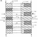
도 1은 본 발명에 따른 반도체(100)의 하나의 실시예의 평면도다. 반도체(100)는 일반적으로 듀얼 게이트 구조로 언급될 수 있다. 반도체(100)는 금속-절연체-반도체(MIS) 디바이스로 실행될 수 있다.1 is a plan view of one embodiment of a
도 1에서, 반도체(100)의 복수의 레벨들 또는 층들이 도시되어 있다. 도 1에 도시된 구조는 제 1 트렌치(111) 및 제 2 트렌치(112)로 예시된, 소스 트렌치들로 알려진 다수의 병렬 트렌치들을 포함한다. 게이트 트렌치로 알려진 제 3 트렌치(113)는, 제 1 및 제 2 트렌치들의 사이에서 제 1 및 제 2 트렌치들에 병렬하고 있다. 각 한 쌍의 소스 트렌치들 사이에 게이트 트렌치가 존재하는, 불특정 수의 소스 트렌치들이 있을 수 있다. 아래에서 서술하듯, 트렌치들(111, 112, 113)은 산화물로 둘러쌀 수 있고 그 후, 예를 들어, 폴리실리콘으로 채워질 수 있다.In FIG. 1, a plurality of levels or layers of
도 1에 도시되어 있는 바와 같이, 제 1 금속층(121)은 트렌치들의 일측 단부에 형성되며, 제 2 금속층(122)은 트렌치들의 반대측 단부에 형성된다. 제 1 및 제 2 금속층들은 동일한 평면에 있으나 서로 물리적으로 이격되어 있다.As shown in FIG. 1, a
제 1 금속층(121)은 소스 금속층으로 알려져 있다. 소스 금속층(121)은 소스 트렌치들(111 및 112) 내의 폴리실리콘과 131 및 132로 식별되는 위치에서 접촉한다. 소스 금속층(121)과의 접촉은 소스 트렌치들 내의 폴리실리콘 상에서 직접 이루어진다.The
제 2 금속층(122)은 게이트 금속층으로 알려져 있다. 게이트 금속층(122)은 게이트 트렌치(11) 내의 폴리실리콘과 133으로 식별되는 위치에서 접촉한다. 게이트 금속층(122)과의 접촉은 게이트 트렌치들 내의 폴리실리콘 상에서 직접 이루어진다. 하나의 실시예에서, 게이트 트렌치들의 넓이는 제 2 금속층(122) 아래에 있는 트렌치들의 단부에서 더 넓다. 즉, 게이트 트렌치들은 게이트 금속층과 접촉하는 지점에서 바깥으로 폭이 넓어진다. 도 1에서 도시되어 있듯이 게이트 트렌치들은 게이트 접점보다 넓다.The
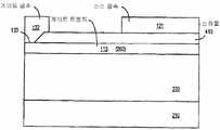
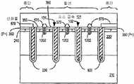
도 2는 도 1에 도시된 A-A 절개선에 따른 단면도이다. 도 2에 도시된 구조(100)의 부분은 소스 트렌치들(111, 112), 추가적인 소스 트렌치들(표시하지 않음), 및 게이트 트렌치(113), 추가적인 게이트 트렌치들(표시하지 않음)을 포함한다.2 is a cross-sectional view taken along line A-A in Fig. The portion of
도 2의 실시예에서, 소스 트렌치들과 게이트 트렌치들은 적층판(laminate) 또는 n+ 영역(210) 및 n형-도핑 에피택셜 영역(n-doped epitaxial region: 220)을 포함하는 기판에 형성된다. 소스 트렌치들은 게이트 트렌치들보다 깊이가 깊다; 소스 트렌치들은 에피택셜 영역(220) 및 n+ 영역(210) 속으로 확장하지만, 게이트 트렌치들은 그러하지 않는다.In the embodiment of FIG. 2, the source trenches and gate trenches are formed in a substrate comprising a laminate or n +
소스 트렌치들과 게이트 트렌치들은 산화막(230)으로 둘러싸일 수 있다. P형 바디 영역들, 이를 테면 p형 바디 영역(240) 또한 소스 트렌치들과 게이트 트렌치들 사이에서 기판에 형성될 수 있다. 소스 영역들, 이를테면 소스 영역(250) 또한 소스 트렌치들과 게이트 트렌치들 사이에서 기판에 형성될 수 있다. 드레인 영역(도시되지 않음)이 n+영역(210) 아래 층으로 실행될 수 있다.The source trenches and the gate trenches may be surrounded by an
도 2의 예에서, 소스 영역들은 반복되는 n+ 영역들이다. 그러나, 도 3에 도시된 하나의 실시예에서, n+ 소스 영역들은 p+ 영역들(350)에 의해 분리된다. 도 3에 도시되어 있는 바와 같이, n+ 소스 영역들(250)과 p+ 영역들(350)은 교번한다. 즉, n+ 소스 영역들(250)은 p+ 영역들(350) 사이에 위치하고, p+ 영역들은 n+ 소스 영역들 사이에 위치한다. P+ 영역들(350)은 p형 바디 영역(240)에 대한 전기적 접촉을 제공하는데 이용된다. 그에 따라, 동일한 소스 금속층이 [p+ 영역들(350)을 통해] p+ 바디 영역들(240)과 n+ 소스 영역들(250) 모두에 전기적 접촉이 가능하다.In the example of FIG. 2, the source regions are repeated n + regions. However, in one embodiment shown in FIG. 3, the n + source regions are separated by p +
아래에 더 상세히 설명될 바와 같이, 소스 및 게이트 트렌치들 내의 폴리실리콘(260)의 상면들(도 2), 소스 트렌치들 위 산화막들(230)의 노출 면들은 트렌치들 사이에 있는 메사들과 높이가 동일하다. 이는 많은 이점을 제공하는데, 이 또한 아래에서 설명하기로 한다.As will be described in greater detail below, the top surfaces (FIG. 2) of
도 2에서 도시된 구조(100)의 끝에서[즉, 금속층(122) 아래의 영역에서; 도 1 참조], 산화물 영역들(270)이 소스 트렌치들 및 소스 트렌치들과 게이트 트렌치들 사이의 메사들 위로 형성되어 있으나, 게이트 트렌치들 위로는 형성되지 않음으로써, 게이트 트렌치들 내의 폴리실리콘(260)이 게이트 금속층(122)에 노출된다. 따라서, 게이트 금속층 (122)은, (133)의 게이트 금속 접점에 예시된 바처럼 게이트 트렌치들 내의 폴리실리콘과 물리적 및 전기적 접촉이 가능해진다.At the end of the
도 4는 도 1에 도시된 B-B 절개선에 따른 단면도이다. 도 4에 도시된 구조(100)의 부분은 게이트 트렌치(113), 소스 금속층(121), 게이트 금속층(122), 에피택셜 영역(220), 및 n+ 영역(210)을 포함한다. 소스 금속층과 게이트 금속층들은 동일한 평면에 있다.4 is a cross-sectional view taken along line B-B in Fig. The portion of the
산화막(410)은 게이트 금속층(122) 아래의 게이트 트렌치들 부분을 제외하고 게이트 트렌치들을 덮음으로써, 게이트 트렌치들 내의 폴리실리콘(260)을 게이트 금속층에 노출시킨다. 그에 따라, 게이트 금속층(122)은 (133)의 게이트 금속 접점에 예시된 바처럼 게이트 트렌치들 내의 폴리실리콘과 물리적 및 전기적 접촉이 가능해진다.The
도 5는 도 1에 도시된 C-C 절개선에 따른 단면도이다. 도 5에 도시된 구조(100)의 부분은 소스 트렌치들(111 및 112), 및 추가적인 소스 트렌치들(표시하지 않음), 그리고 게이트 트렌치(113), 및 추가적인 게이트 트렌치들(표시하지 않음)을 포함한다.5 is a cross-sectional view taken along line C-C in Fig. The portion of
아래에서 상세하게 설명하게 될 바와 같이, 소스 및 게이트 트렌치들 내의 폴리실리콘(260)의 상면들, 산화막들(230)의 노출 면들, 및 트렌치들 사이에 있는 메사들의 높이는 동일하다. 이는 많은 이점을 제공하는데, 이 또한 아래에서 설명하기로 한다.As will be described in greater detail below, the top surfaces of the
도 5에 도시된 구조(100)의 단부에서[즉, 소스 금속층(121) 아래의 영역에서; 도 1 참조], 산화물 영역들(570)은 게이트 트렌치들 위로 형성되어 있으나 소스 트렌치들 위로 형성되어 있지 않다. 또한, 산화물 영역들(570)은 종단 영역들(termination regions) 내 n+ 소스 영역들 위에 형성되어 있으나, 활성 영역(active region) 내 n+ 소스 영역들 위에 형성되지 않는다. 결과적으로, 소스 트렌치들 내 폴리실리콘(260)과 활성 영역 내 n+소스 영역들[예를 들어, n+ 소스 영역 (250)]은 소스 금속층(121)에 노출된다. 그에 따라 소스 금속층(121)은, 131 및 132의 소스 금속 접점에 예시된 바처럼 소스 트렌치들 내 폴리실리콘 및 n+ 영역들과 물리적 및 전기적 접촉이 가능해진다.At the end of the
도 6은 도 1에 도시된 D-D 절개선에 따른 단면도이다. 도 6에 도시된 구조(100)의 부분은 소스 트렌치(111), 소스 금속층(121), 게이트 금속층(122), 및 n+ 영역(210)을 포함한다. 소스 및 게이트 금속층들은 동일한 평면에 있다.6 is a cross-sectional view taken along line D-D in Fig. The portion of
산화막(610)이 소스 금속층(121) 아래의 트렌치들 부분을 제외하고 소스 트렌치들을 덮음으로써, 소스 트렌치들 내 폴리실리콘(260)이 소스 금속층에 노출된다. 그에 따라, 소스 금속층(121)은, (131)의 소스 금속 접점에 예시된 바처럼 소스 트렌치들 내 폴리실리콘(260)과 물리적 및 전기적 접촉이 가능해진다.The
도 7A 및 7B는 도 1에 부분적으로 예시된 디바이스와 같은 반도체 디바이스들의 제조에 이용되는 하나의 실시예 과정의 순서도(700)를 예시하고 있다. 비록 특정한 단계들이 순서도(700)에 개시되어 있지만, 이들은 예시적인 것이다. 즉, 본 발명에 따른 실시예들은 다양한 기타 단계들을 수행하거나 순서도(700)에 인용된 단계들의 변형들을 수행하는 데에 적절하다. 순서도(700)는, 본 발명의 실시예에 따른 반도체 디바이스의 제조에 있어서 일부 선정된 단계들을 도시하는 단면도인 도 8-17과 결합하여 설명된다. 특정의 잘 알려진 단계들은 이후의 설명에서 제외한다. 예를 들어, 마스크의 형성과 제거와 관련한 공정은 제시되지 않는다.FIGS. 7A and 7B illustrate a
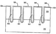
도 8을 함께 참조하면, 도 7의 블록(702)에서 트렌치들(802)은 n+ 영역(210) 및 에피택셜 영역(220)을 포함하는 기판/적층판에 형성된다. 트렌치들(802)을 형성하기 위하여 에칭 공정이 이용될 수 있다. 트렌치들(802)은 소스 트렌치들로 이용된다.8,
도 9를 함께 참조하면, 블록(704)에서 트렌치들(802)의 측벽 및 하단부를 따라, 그리고 상기 트렌치들 사이의 메사들(906) 위에 산화막(904)이 침적된다.9, at
도 10을 함께 참조하면, 블록(706)에서 트렌치들(802) 내에 폴리실리콘(1008/poly-1)이 침적된다. 각 트렌치들은 poly-1이 넘칠 만큼 채워도 된다. 하나의 실시예에서, 평평한 면을 형성하기 위하여 poly-1을 연마하는 제 1 폴리실리콘 연마 공정(예를 들어, CMP 공정)이 이용된다. 그 후 poly-1은 인접 산화막(904)에 상대적으로 만입되도록 (예를 들어, 플라즈마로) 백에칭 할 수 있다.10,
도 11을 함께 참조하면, 블록(708)에서 산화막 연마 공정(예를 들어, CMP 공정)이 균등한(평평하고 매끄러운) 표면(1110)을 형성하기 위해 사용된다. 구체적으로, 메사들 위의 산화막(904)이 제거되어, 산화막의 노출 면들[트렌치들(802)의 측벽을 따라, 산화막(904)의 잔여 부분의 단부들]이 인접한 면들/메사들과 높이가 동일하게 된다. 또한, 트렌치들(802)로부터 돌출하는 poly-1의 어떠한 부분들도 제거되어, poly-1의 노출 면들 또한 인접한 면들/메사들과 높이가 동일하게 된다.11, an oxide film polishing process (e.g., a CMP process) is used at
산화막 연마 공정(예를 들어 CMP 공정) 중에, 침적을 통해 추가적인 산화물을 부가하거나 제거를 함으로써 평평하면서 동시에 매끈한 표면(1110)을 얻을 수 있다. 실용적인 범위 내에서 표면(1110)은 결함(예를 들어, dips, pits, scratches)이 없는 것이 유리하다. 후속 단계(블록 712)에서 폴리실리콘(poly-2)이 게이트 트렌치들로 이용되는 트렌치들 내에 침적된다; 만약 표면(1110)이 실질적으로 평평하고 매끈하지 않다면, poly-2는 이러한 결함에 침전되어, 잠재적으로 스트링어(stringer)를 형성할 수 있다.During the oxide polishing process (e.g., a CMP process), additional oxide may be added or removed through the deposition to obtain a flat and
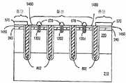
도 12를 참조하면, 블록(710)에서, 기판에 트렌치들(1202)이 형성된다. 트렌치들(1202)을 형성하는 데에는 에칭 공정이 이용될 수 있다. 트렌치들(1202)은 게이트 트렌치들로 이용되며 소스 트렌치들(802)보다 깊이가 낮다. 도 1에서 도시되어 있는 바와 같이가, 트렌치들(1202)의 한쪽 단부 - 게이트 금속 접점이 형성되는 단부- 에서 트렌치들(1202)의 넓이가 넓어진다.Referring to FIG. 12, at block 710,
도 12를 함께 참조하면 블록(712)에서, 트렌치들(1202)의 측벽들 및 하단부들을 따라, 그리고 트렌치들(1202)과 트렌치들(802) 사이의 메사들(1206) 위로 얇은 게이트 산화막(1204)이 생성된다.12, at
도 13을 참조하면 블록(714)에서, 폴리실리콘(1308/poly-2)이 트렌치들(1202) 내에 침적된다. 각 트렌치는 poly-2를 넘치게 채울 수 있는데, 이 경우 제 2 폴리실리콘 연마 공정(예를 들어 CMP 공정)이 평평한 면을 또 한 번 생성시키기 위해 사용된다. 그 후 poly-2는 인접 산화막에 상대적으로 만입되도록 (예를 들어, 플라즈마로) 백에칭 할 수 있다.Referring to FIG. 13, at
도 13를 계속하여 참조하면, 하나의 실시예에서, p형 바디 영역들(240)이 트렌치들(802 및 1202) 사이의 영역에서 형성될 수 있다.With continued reference to Figure 13, in one embodiment, p-
도 14를 함께 참조하면 블록(716)에서, 트렌치들(802 및 1202) 사이의 영역에서 영역들(1450)이 형성된다. 도 3과 결합하여 위에서 설명한 바와 같이, 영역들(1450)은 교번하는 n+ 소스 영역들(250) 및 p+ 영역들(350)을 포함한다. 즉, 도 3에서 도시되어 있는 바와 같이 n+ 소스 영역들(250)과 p+ 소스 영역들(350)은 상호 교번한다.14, at
도 15를 함께 참조하면 블록(718)에서, 소스 금속 영역의 지정된 위치에 산화물(570)이 침적된다. 구체적으로, 산화막이 침적되고, 그 이후 선택적으로 제거됨으로써, 소스 금속 영역에서 산화물(570)이 종단 영역들 내 및 게이트 트렌치들(1202) 위에 남아서, 영역들(1450)[예를 들어, 교번하는 n+ 소스 영역들(250)과 p+ 영역들(350)]이 활성 영역에 노출되고 소스 트렌치들(802)이 종단 및 활성 영역에 노출된다.15, at
결과적으로, 도 5에서 보는 바와 같이, 이후 소스 금속층(121)이 침적된 경우에 소스 트렌치들(111 및 112) 그리고 n+ 소스 영역들(250)에 대한 물리적 및 전기적 접촉이 이루어진다. 또한, 도 16에서 보는 바와 같이, 이후 소스 금속층(121)이 침적된 경우, p+ 영역들(350)에 대한 전기적 및 물리적 접촉 그리고 그에 따른 p형 바디 영역들(240)에 대한 전기적 접촉이 이루어진다. 따라서, 동일한 소스 금속층이 n+ 소스 영역들(250) 및 p형 바디 영역들(240) 모두에 전기적 접촉을 하게 된다.As a result, physical and electrical contacts are made to the
또한, 도 17을 참조하면, 산화물(270)이 게이트 금속 영역의 지정된 위치에 침적된다. 구체적으로, 산화막이 침적되고, 그 이후 선택적으로 제거됨으로써, 게이트 금속 영역에서 산화물(270)이 소스 트렌치들(802) 및 영역들(1450)[n+ 소스 영역들(250) 및 p+ 소스 영역들(350)]의 위에 남아있어, 게이트 트렌치들(1202)을 노출시키게 된다. 결과적으로, 이후에 게이트 금속층(122)이 침적되는 경우, 도 2에서 도시하듯이 게이트 트렌치들에 대한 물리적 및 전기적 접촉이 이루어진다. (‘W’ 방향을 따라 측정한) 게이트 트렌치의 넓이는 게이트 금속층(122)과 게이트 트렌치의 접점의 넓이보다 적다.Also, referring to FIG. 17, an
요약하면, 본 발명에 따른 실시예들은, 각각 연결된 독립적인 게이트 및 소스 트렌치들 내에 분리된 폴리실리콘 층들을 가지는 듀얼 게이트 구조들을 포함하는 트렌치-게이트 디바이스(예를 들어, MIS 디바이스들)의 구조들 및 제조 방법들과 관련된다. 듀얼 게이트 구조들은 게이트 트렌치 내 게이트 폴리실리콘(poly-2) 층을 게이트 전극에 연결하는 게이트 접점, 그리고 소스 트렌치 내 폴리실리콘(poly-1) 층을 소스 전극에 연결하는 소스 접점을 통해 실행된다. 소스 접점 그리고 게이트 접점은 동일한 평면에 있다.In summary, embodiments in accordance with the present invention relate to structures of trench-gate devices (e.g., MIS devices) including dual gate structures with separate gate and source polysilicon layers in each connected trenches And manufacturing methods. The dual gate structures are implemented through a gate contact connecting the gate polysilicon (poly-2) layer in the gate trench to the gate electrode and a source contact connecting the polysilicon (poly-1) layer in the source trench to the source electrode. The source contact and the gate contact are on the same plane.
CMP 공정은 위 디바이스들의 제조를 용이하게 하기 위하여 이용된다. CMP의 사용은 소스 및 게이트 트렌치들 내의 폴리실리콘 그리고 각 소스 트렌치 상위의 산화물을 평탄화시키는 것을 가능하게 함으로써, 구조에 대한 향상된 제어와 향상된 공정 마진의 결과를 가져오고, 그에 따라 성능의 향상으로 이어진다. 예를 들어, 평탄화 과정은 포토리소그래피(photolithography) 중의 초점심도(depth of focus)를 향상시킨다. 그에 따라, 재료들을 더욱 정확하고 균일하게 침적시킬 수 있고, 깊이가 더 낮은 트렌치들이 형성될 수 있다. 결과적으로, 디바이스들이 더욱 작은 크기로 조정이 가능해진다.The CMP process is used to facilitate fabrication of the above devices. The use of CMP makes it possible to planarize the polysilicon in the source and gate trenches and the oxide above each source trench, resulting in improved control of the structure and improved process margin resulting in improved performance. For example, the planarization process improves the depth of focus during photolithography. Thereby, the materials can be deposited more accurately and uniformly, and trenches with lower depths can be formed. As a result, the devices can be adjusted to a smaller size.
본 발명에 따른 실시예들은 중전압정격(60-150V) 트렌치 전력 MOS 디바이스 및 고전압정격(150-300V) 트렌치 전력 MOS 디바이스들에 이용될 수 있다.Embodiments in accordance with the present invention may be used for medium voltage rated (60-150V) trench power MOS devices and high voltage rated (150-300V) trench power MOS devices.
요약하면, 반도체 디바이스들의 실시예들, 그리고 당해 디바이스들을 제조하는 방법의 실시예들이 제시되어 있다. 앞서 언급한 본 발명의 특정 실시예들은 예시와 서술의 목적을 위해 제공되었다. 그것들은 개시된 발명의 특정 형태들이 하나도 빠뜨리지 않은 것임을 또는 개시된 특정한 형태로 본 발명을 제한하는 것을 의도하지 않았으며, 상기 내용을 고려한 수많은 수정과 변형들이 가능하다. 실시예들은, 다른 동업자들이 발명 및 특정한 이용을 고려한 발명의 다양한 변형을 갖춘 다양한 실시예들을 가장 잘 활용할 수 있도록, 발명의 원리와 그것의 실제적 적용을 가장 잘 설명하기 위하여 선택되었고 순서대로 제시되었다. 본 발명의 범위는 본 명세서에 첨부된 청구 범위 및 그 등가물에 의해 정의되는 것을 의도하고자 한다.In summary, embodiments of semiconductor devices and embodiments of methods of fabricating such devices are presented. The foregoing specific embodiments of the invention have been presented for purposes of illustration and description. They are not intended to be exhaustive or to limit the invention to the particular forms disclosed and that numerous modifications and variations are possible in light of the above teachings. The embodiments have been chosen and illustrated in order to best explain the principles of the invention and its practical application, so that other persons skilled in the art can best utilize the various embodiments having various modifications of the invention in consideration of the invention and the particular use. The scope of the invention is intended to be defined by the claims appended hereto and their equivalents.
본 명세서에 제시된 모든 요소들, 절차들과 단계들은 바람직하게 포함된다. 이러한 요소들, 절차들과 단계들은 당업계에서 공지된 다른 요소들, 절차들과 단계들에 의해 교체되거나 또는 모두 삭제될 수 있음을 이해해야 한다.All elements, procedures and steps presented herein are preferably included. It is to be understood that such elements, procedures and steps may be replaced or eliminated by other elements, procedures and steps known in the art.
대략적으로, 본 명세서는 다음과 같이 개시한다: 기재에 형성된 깊은 트렌치들 내에 제 1 폴리실리콘(poly-1)이 침적된다. Poly-1의 노출 면을 평탄화시켜 면이 인접면들과 동일한 높이가 되도록 제 1 폴리실리콘 연마 공정을 수행한다. 이후, 깊이가 낮은 트렌치들이 깊은 트렌치들 사이의 기판에 형성되고, 제 2 폴리실리콘(poly-2)이 깊이가 낮은 트렌치들 내에 침적된다. Poly-2의 노출 면을 평탄화시켜 면이 인접면들과 동일한 높이가 되도록 제 1 폴리실리콘 연마 공정을 수행한다. 그 이후 poly-1 및 poly-2에 대한 금속 접점들이 형성된다.
Approximately, the present disclosure begins as follows: a first polysilicon (poly-1) is deposited in deep trenches formed in a substrate. The exposed surface of Poly-1 is planarized to perform a first polysilicon polishing process so that the surfaces are flush with the adjacent surfaces. Subsequently, low depth trenches are formed in the substrate between the deep trenches, and a second polysilicon (poly-2) is deposited in the low depth trenches. The exposed surface of Poly-2 is planarized to perform a first polysilicon polishing process so that the surfaces are flush with the adjacent surfaces. Metal contacts for poly-1 and poly-2 are then formed.
개념들(concepts)Concepts
본 명세서는 적어도 다음과 같은 개념들을 개시한다.The present disclosure discloses at least the following concepts.
개념 1:Concept 1:
기판(substrate)에 형성된 제 1 트렌치(trench) 및 제 2 트렌치 내에 제 1 폴리실리콘을 침적(deposit)시키는 과정;Depositing a first polysilicon in a first trench and a second trench formed in a substrate;
상기 제 1 폴리실리콘의 노출 면을 평탄화하여 상기 면이 인접 면과 동일한 높이가 되도록 제 1 폴리실리콘 연마 공정(polishing process)을 수행하는 과정;Performing a first polysilicon polishing process so that the exposed surface of the first polysilicon is planarized to have the same height as the adjacent surface;
상기 제 1 폴리실리콘 연마 공정을 수행한 후, 상기 제 1 및 제 2 트렌치보다 깊이가 낮은(shallow) 제 3 트렌치를 상기 제 1 트렌치과 제 2 트렌치 사이에서 기판에 형성하는 과정;Forming a third shallow trench, which is shallower than the first and second trenches, on the substrate between the first trench and the second trench after performing the first polysilicon polishing process;
상기 제 3 트렌치 내에 제 2 폴리실리콘을 침적시키는 과정;Depositing a second polysilicon in the third trench;
상기 제 2 폴리실리콘의 노출 면을 평탄화하여 상기 면이 인접 면과 동일한 높이가 되도록 제 2 폴리실리콘 연마 공정을 수행하는 과정; 및Performing a second polysilicon polishing process so that the exposed surface of the second polysilicon is planarized to have the same height as the adjacent surface; And
상기 제 1 폴리실리콘에 제 1 금속 접점(metal contact)을 형성하고 상기 제 2 폴리실리콘에 제 2 금속 접점을 형성하는 과정;Forming a first metal contact on the first polysilicon and a second metal contact on the second polysilicon;
을 포함하는 것을 특징으로 하는 듀얼 게이트 반도체 디바이스 (dual gate semiconductor device)의 제조 방법.Wherein the first gate electrode and the second gate electrode are electrically connected to each other.
개념 2:Concept 2:
개념 1에 있어서,In concept 1,
상기 제 1 폴리실리콘을 침적하기에 앞서, 상기 제 1 및 제 2 트렌치들 내 및 상기 제 1 및 제 2 트렌치들 사이의 상기 기판 상에 산화물(oxide)을 침적시키는 과정; 및Depositing oxide on the substrate in the first and second trenches and between the first and second trenches prior to depositing the first polysilicon; And
상기 산화물을 평탄화하기 위하여 산화물 연마 공정을 수행하는 과정;Performing an oxide polishing process to planarize the oxide;
을 더 포함하는 것을 특징으로 하는 제조 방법.≪ / RTI >
개념 3:Concept 3:
개념 2에 있어서, 상기 제 1 및 제 2 폴리실리콘 연마 공정과 상기 산화물 연마 공정은 화학적 기계적 연마 공정(chemical mechanical polishing processes)을 포함하는 것을 특징으로 하는 제조 방법.The method of claim 2, wherein said first and second polysilicon polishing processes and said oxide polishing process comprise chemical mechanical polishing processes.
개념 4:Concept 4:
개념 1에 있어서, 상기 제 1 금속 접점은 상기 제 1 폴리실리콘 상에 직접 위치하면서 접촉되어 있으며, 상기 제 2 금속 접점은 상기 제 2 폴리실리콘 상에 직접 위치하면서 접촉되어 있는 것을 특징으로 하는 제조 방법.The method of claim 1, wherein the first metal contact is in direct contact with and on the first polysilicon, and the second metal contact is in direct contact with the second polysilicon. .
개념 5:Concept 5:
개념 1에 있어서, 상기 제 1 금속 접점은 제 1 금속층(metal layer)의 일부이고, 상기 제 2 금속 접점은 제 2 금속층의 일부이며, 상기 제 1 및 제 2 금속층들은 동일한 평면(surface plane)에 있으나 서로 물리적으로 이격되어 있는 것을 특징으로 하는 제조 방법.The first metal contact is a part of a first metal layer and the second metal contact is a part of a second metal layer and the first and second metal layers are on the same surface plane But are physically spaced apart from each other.
개념 6:Concept 6:
개념 1에 있어서, 상기 제 3 트렌치는 상기 제 2 금속 접점보다 넓은 것을 특징으로 하는 제조 방법.The method of claim 1, wherein the third trench is wider than the second metal contact.
개념 7:Concept 7:
기판에 형성되어 있는 소스 트렌치(source trench);A source trench formed in the substrate;
상기 기판에 형성되어 있고 상기 소스 트레인과 병렬(parallel)인 게이트 트렌치;A gate trench formed in the substrate and parallel to the source train;
상기 소스 트렌치의 제 1 단부(end)에서 소스 트렌치 내의 제 1 폴리실리콘에 연결되어 있고, 상기 제 1 폴리실리콘의 제 1 표면 상에 직접 위치하면서 접촉되어 있는 소스 접점(source contact); 및A source contact connected to the first polysilicon in the source trench at a first end of the source trench and in direct contact with and on the first surface of the first polysilicon; And
상기 제 1 단부에 대향하는 상기 게이트 트렌치의 제 2 단부에서 게이트 트렌치 내의 제 2 폴리실리콘에 연결되어 있고, 상기 제 2 폴리실리콘의 제 2 표면 상에 직접 위치하면서 접촉되어 있는 게이트 접점(gate contact);A gate contact coupled to the second polysilicon in the gate trench at a second end of the gate trench opposite the first end and in direct contact with and on the second surface of the second polysilicon, ;
을 포함하는 것을 특징으로 하는 반도체 디바이스.≪ / RTI >
개념 8:Concept 8:
개념 7에 있어서, 상기 소스 접점은 제 1 금속층의 일부이고, 상기 게이트 접점은 제 2 금속층의 일부이며, 상기 제 1 및 제 2 금속층들은 동일한 평면에서 물리적으로 서로 이격되어 있는 것을 특징으로 하는 반도체 디바이스.The semiconductor device of claim 7, wherein the source contact is part of a first metal layer, the gate contact is part of a second metal layer, and the first and second metal layers are physically spaced from each other in the same plane. .
개념 9:Concept 9:
개념 7에 있어서, 상기 제 1 및 제 2 표면 모두 상기 게이트 및 소스 트렌치들에 의해 형성된 메사(mesa)의 표면과 동일한 높이인 것을 특징으로 하는 반도체 디바이스.The semiconductor device of claim 7, wherein both the first and second surfaces are flush with the surface of the mesa formed by the gate and source trenches.
개념 10:Concept 10:
개념 7에 있어서, 상기 게이트 트렌치는 상기 제 2 단부에서 더 넓은 것을 특징으로 하는 반도체 디바이스.The semiconductor device of claim 7, wherein the gate trench is wider at the second end.
개념 11:Concept 11:
개념 7에 있어서, 상기 게이트 트렌치는 상기 게이트 접점보다 넓은 것을 특징으로 하는 반도체 디바이스.The semiconductor device according to concept 7, wherein the gate trench is wider than the gate contact.
개념 12:Concept 12:
기판에 제 1 트렌치 및 제 2 트렌치를 형성하고, 상기 제 1 및 제 2 트렌치들은 제 1 메사(mesa)에 의해 분리시키는 과정;Forming a first trench and a second trench in a substrate, and separating the first and second trenches by a first mesa;
상기 제 1 및 제 2 트렌치들의 내부와 상기 제 1 메사 위에 제 1 산화막(oxide layer)을 형성한 다음, 상기 제 1 및 제 2 트렌치들 내에 제 1 폴리실리콘을 침적시키는 과정;Depositing an oxide layer in the first and second trenches and on the first mesa and then depositing a first polysilicon in the first and second trenches;
평평한 표면을 형성하기 위하여, 상기 제 1 폴리실리콘의 적어도 일부를 제거하기 위한 제 1 폴리실리콘 연마 공정을 수행하고 상기 제 1 산화층의 적어도 일부를 제거하기 위한 산화막 연마 공정을 수행하는 과정;Performing a first polysilicon polishing process to remove at least a portion of the first polysilicon and performing an oxide film polishing process to remove at least a portion of the first oxide layer to form a flat surface;
상기 제 1 연마 공정과 산화막 연마 공정 이후에, 제 1 트렌치 및 제 2 트렌치 사이의 상기 제 1 메사에 제 3 트렌치를 형성하여, 상기 제 1 트렌치와 제 3 트렌치는 제 2 메사에 의해 분리되고, 상기 제 2 트렌치 및 제 3 트렌치는 제 3 메사에 의해 분리되며, 상기 제 3 트렌치는 상기 제 1 트렌치 및 제 2 트렌치보다 깊이가 낮도록 하는 과정;Forming a third trench in the first mesa between the first trench and the second trench after the first polishing step and the oxide film polishing step such that the first trench and the third trench are separated by the second mesa, The second trench and the third trench being separated by a third mesa, the third trench being lower in depth than the first trench and the second trench;
상기 제 3 트렌치 내부와 상기 제 2 및 제 3 메사 위에 제 2 산화막을 형성한 후, 제 2 폴리실리콘을 상기 제 3 트렌치 내에 침적시키는 과정; 및Depositing a second polysilicon in the third trench after forming a second oxide film on the third trench and on the second and third mesas; And
상기 제 2 폴리실리콘의 적어도 일부를 제거하기 위한 제 2 폴리실리콘 연마 공정을 수행하는 과정;Performing a second polysilicon polishing process to remove at least a portion of the second polysilicon;
을 포함하는 것을 특징으로 하는 듀얼 게이트 반도체 디바이스의 제조 방법.And a second gate electrode formed on the first gate electrode.
개념 13:Concept 13:
개념 12에 있어서, 상기 제 1 폴리실리콘에 제 1 금속 접점을 형성하고, 상기 제 2 폴리실리콘에 제 2 금속 접점을 형성하여, 상기 제 1 금속 접점이 상기 제 1 폴리실리콘 상에 직접 위치하면서 접촉하고, 상기 제 2 금속 접점이 상기 제 2 트렌치에서 제 2 폴리실리콘 상에 직접 위치하면서 접촉하도록 하는 과정을 더 포함하는 것을 특징으로 하는 제조 방법.The method of claim 12 further comprising forming a first metal contact on the first polysilicon and forming a second metal contact on the second polysilicon so that the first metal contact is positioned directly on the first polysilicon, And allowing the second metal contact to be in direct contact with the second polysilicon in the second trench.
개념 14:Concept 14:
개념 13에 있어서, 상기 제 1 금속 접점은 제 1 금속층의 일부이고, 상기 제 2 금속 접점은 제 2 금속층의 일부이며, 상기 제 1 및 제 2 금속층들은 동일한 평면에 있으나 서로 물리적으로 이격되어 있는 것을 특징으로 하는 제조 방법.The first metal contact is a part of a first metal layer and the second metal contact is a part of a second metal layer and the first and second metal layers are on the same plane but physically spaced from each other .
개념 15:Concept 15:
개념 13에 있어서, 상기 제 1 및 제 2 폴리실리콘 연마 공정 및 상기 산화막 연마 공정은 화학적 기계적 연마 공정을 포함하는 것을 특징으로 하는 제조 방법.13. The manufacturing method according to concept 13, wherein the first and second polysilicon polishing processes and the oxide polishing process include a chemical mechanical polishing process.
Claims (19)
Translated fromKorean병렬적으로 기판에 형성되어 있는 제 1 트렌치(trench) 내 및 제 2 트렌치 내에 산화물을 침적(deposit)시키는 단계 - 상기 산화물은 상기 제 1 트렌치 및 제 2 트렌치 사이에 있는 메사(mesa)의 상부 표면 위에도 침적되어, 상기 메사의 상기 상부 표면 위에 위치하는 상부 표면을 갖는 산화막을 형성함 - 와,
상기 제 1 트렌치 내 및 상기 제 2 트렌치 내에 제 1 폴리실리콘을 침적시키는 단계 - 상기 제 1 및 제 2 트렌치들 내의 상기 제 1 폴리실리콘의 상부 표면들은 노출됨 - 와,
상기 산화물을 침적시키는 단계 및 상기 제 1 폴리실리콘을 침적시키는 단계 이후에, 제 1 폴리실리콘 연마 공정을 수행하여, 상기 제 1 폴리실리콘 연마 공정 이후에 상기 제 1 폴리실리콘의 상기 상부 표면들이 상기 메사 위의 상기 산화막의 상부 표면과 동일한 높이가 되도록 상기 제 1 폴리실리콘의 상기 상부 표면들을 평탄화하는 단계와,
상기 제 1 폴리실리콘 연마 공정 이후에, 산화물 연마 공정을 수행하여, 상기 산화물 연마 공정 이후에 상기 제 1 폴리실리콘의 상기 상부 표면들이 상기 메사의 상기 상부 표면과 동일한 높이가 되도록, 상기 메사 위로부터 상기 산화막을 제거하고 상기 제 1 폴리실리콘의 상부 표면들로부터 제 1 폴리실리콘을 제거하는 단계와,
상기 산화물 연마 공정 이후에, 상기 제 1 트렌치 및 제 2 트렌치의 사이에서 상기 메사 내에 제 3 트렌치를 형성하는 단계 - 상기 제 3 트렌치는 상기 제 1 및 제 2 트렌치들에 병렬적으로 위치하나, 상기 제 1 및 제 2 트렌치들보다 얕음(shallow) - 와,
상기 제 3 트렌치 내에 제 2 폴리실리콘을 침적시키는 단계 - 상기 제 3 트렌치 내의 제 2 폴리실리콘의 상부 표면은 노출됨 - 와
상기 제 2 폴리실리콘을 침적시키는 단계 이후에, 제 2 폴리실리콘 연마 공정을 수행하여, 상기 제 2 폴리실리콘의 상부 표면이 상기 메사의 상기 상부 표면과 동일한 높이가 되도록 상기 제 2 폴리실리콘의 상기 상부 표면을 평탄화하는 단계와,
상기 제 1 폴리실리콘의 표면에 연결(coupled) 및 접촉되어 있는 소스 금속층의 소스 접점(source contact)을 형성하고 - 상기 소스 금속층은, 상기 제 1 폴리 실리콘 및 상기 제 2 폴리실리콘의 상기 상부 표면들 위로 뻗어(extend) 있고, 상기 메사와 동일한 높이임 -, 상기 제 2 폴리실리콘의 표면에 연결 및 접촉되어 있는 게이트 금속층의 게이트 접점(gate contact)을 형성하는 - 상기 기판 상에 형성되어 있는 상기 게이트 금속층은, 상기 제 1 폴리실리콘 및 상기 제 2 폴리실리콘의 상기 상부 표면들 위로 뻗어 있고, 상기 메사와 동일한 높이임 - 단계
를 포함하는
반도체 디바이스의 제조 방법.
A method of manufacturing a semiconductor device,
Depositing an oxide in a first trench and in a second trench formed in parallel on a substrate, the oxide being deposited on a top surface of a mesa between the first trench and the second trench, And forming an oxide film having an upper surface located on the upper surface of the mesa,
Depositing a first polysilicon in the first trench and in the second trench, the upper surfaces of the first polysilicon in the first and second trenches being exposed;
Performing a first polysilicon polishing process after the step of depositing the oxide and depositing the first polysilicon so that after the first polysilicon polishing step the upper surfaces of the first polysilicon are exposed to the mesas Planarizing the upper surfaces of the first polysilicon so as to be at the same height as the upper surface of the oxide film,
After the first polysilicon polishing step, an oxide polishing process is performed so that after the oxide polishing process, the upper surfaces of the first polysilicon are flush with the upper surface of the mesa, Removing the oxide film and removing the first polysilicon from the upper surfaces of the first polysilicon,
Forming a third trench in the mesa between the first trench and the second trench after the oxide polishing step, the third trench being located in parallel to the first and second trenches, Shallower than the first and second trenches,
Depositing a second polysilicon in the third trench, the upper surface of the second polysilicon in the third trench being exposed; and
After the step of depositing the second polysilicon, a second polysilicon polishing process is performed so that the upper surface of the second polysilicon is at the same height as the upper surface of the mesa, Planarizing the surface,
Forming a source contact of a source metal layer that is coupled to and in contact with a surface of the first polysilicon, the source metal layer comprising: And forming a gate contact of a gate metal layer connected to and in contact with the surface of the second polysilicon, wherein the gate contact is formed on the substrate, A metal layer extends over the top surfaces of the first polysilicon and the second polysilicon and is at the same height as the mesa,
Containing
A method of manufacturing a semiconductor device.
상기 제 1 및 제 2 폴리실리콘 연마 공정들과 상기 산화물 연마 공정은 화학적 기계적 연마 공정(chemical mechanical polishing processes)을 포함하는
반도체 디바이스의 제조 방법.
The method according to claim 1,
Wherein the first and second polysilicon polishing processes and the oxide polishing process comprise chemical mechanical polishing processes
A method of manufacturing a semiconductor device.
상기 소스 접점은 상기 제 1 폴리실리콘의 바로 위에 위치하면서 상기 제 1 폴리실리콘과 접촉되어 있으며, 상기 게이트 접점은 상기 제 2 폴리실리콘의 바로 위에 위치하면서 상기 제 2 폴리실리콘과 접촉되어 있는
반도체 디바이스의 제조 방법.
The method according to claim 1,
Wherein the source contact is located directly above the first polysilicon and is in contact with the first polysilicon and the gate contact is located directly above the second polysilicon and is in contact with the second polysilicon
A method of manufacturing a semiconductor device.
상기 소스 접점은 제 1 금속층의 일부이고, 상기 게이트 접점은 제 2 금속층의 일부이며, 상기 제 1 및 제 2 금속층들은 동일한 평면(surface plane)에 위치하나 서로 물리적으로 이격(isolated)되어 있는
반도체 디바이스의 제조 방법.
The method according to claim 1,
Wherein the source contact is part of a first metal layer and the gate contact is part of a second metal layer and the first and second metal layers are located on a surface plane but physically isolated from each other
A method of manufacturing a semiconductor device.
상기 제 3 트렌치는 상기 게이트 접점보다 넓은
반도체 디바이스의 제조 방법.
The method according to claim 1,
The third trench is wider than the gate contact
A method of manufacturing a semiconductor device.
기판에 병렬적으로 위치하는 제 1 트렌치 및 제 2 트렌치를 형성하는 단계 - 상기 제 1 및 제 2 트렌치들은 상부 표면을 갖는 제 1 메사에 의해 분리(separate)되어 있음 - 와,
상기 제 1 및 제 2 트렌치들의 내부와 상기 제 1 메사의 상부 표면 위에 제 1 산화막을 형성 - 상기 제 1 산화막은 상기 제 1 메사의 상기 상부 표면 위에 위치하는 상부 표면을 갖음 - 하고, 그리고 나서, 상기 제 1 및 제 2 트렌치들 내에 제 1 폴리실리콘을 침적 - 상기 제 1 및 제 2 트렌치들 내의 제 1 폴리실리콘의 상부 표면들은 노출됨 - 시키는 단계와,
상기 제 1 폴리실리콘을 침적시키는 단계 이후에, 제 1 폴리실리콘 연마 공정을 수행하여, 상기 제 1 폴리실리콘의 상기 상부 표면들로부터 상기 제 1 폴리실리콘의 적어도 일부를 제거하는 단계와,
상기 제 1 폴리실리콘 연마 공정이 수행된 후, 상기 제 1 폴리실리콘의 상기 상부 표면들이 상기 제 1 메사의 위에 위치하는 상기 제 1 산화막의 상부 표면에 대하여 상대적으로 만입(recessed)되도록 상기 제 1 폴리실리콘의 상기 상부 표면들을 백에칭(etching back)하는 단계와,
상기 백에칭하는 단계 이후에, 산화물 연마 공정을 수행하여, 상기 산화물 연마 공정이 수행된 후에 상기 제 1 폴리실리콘의 상기 상부 표면들이 상기 제 1 메사의 상기 상부 표면과 동일한 높이가 되도록, 상기 제 1 메사 위로 돌출한 상기 제 1 폴리실리콘의 상기 상부 표면들의 일부와 상기 제 1 메사 위로부터 상기 제 1 산화막을 제거하는 단계와,
상기 제 1 폴리실리콘 연마 공정 및 상기 산화물 연마 공정이 수행된 후에, 제 1 트렌치 및 제 2 트렌치 사이에서 상기 제 1 메사에 제 3 트렌치를 형성하는 단계 - 상기 제 1 및 제 3 트렌치들은 상부 표면을 갖는 제 2 메사에 의해 분리되고, 상기 제 2 및 제 3 트렌치들은 상부 표면을 갖는 제 3 메사에 의해 분리되며, 상기 제 3 트렌치는 상기 제 1 트렌치 및 제 2 트렌치에 병렬적으로 위치하고 상기 제 1 및 제 2 트렌치들보다 얕음 - 와,
상기 제 3 트렌치 내부와 상기 제 2 및 제 3 메사들 위에 제 2 산화막을 형성하고, 그리고 나서, 제 2 폴리실리콘을 상기 제 3 트렌치 내에 침적시키는 단계 - 상기 제 3 트렌치 내의 제 2 폴리실리콘의 상부 표면은 노출됨 - 와,
상기 제 2 폴리실리콘을 침적시키는 단계 이후에, 제 2 폴리실리콘 연마 공정을 수행하여, 상기 제 2 폴리실리콘의 상기 상부 표면이 상기 제 2 메사의 상기 상부 표면 및 제 3 메사의 상기 상부 표면과 동일한 높이가 되도록 상기 제 2 폴리실리콘의 상기 상부 표면을 평탄화하는 단계와,
상기 제 1 폴리실리콘의 표면에 연결 및 접촉되어 있는 소스 금속층의 소스 접점을 형성하고 - 상기 소스 금속층은, 상기 제 1 메사와 동일한 높이인 상기 상부 표면들 위로 뻗도록 상기 기판 상에 형성됨 -, 상기 제 2 폴리실리콘의 표면에 연결 및 접촉되어 있는 게이트 금속층의 게이트 접점을 형성하는 - 상기 게이트 금속층은, 상기 제 2 및 제 3 메사들과 동일한 높이인 상기 제 2 폴리실리콘의 상기 상부 표면 위로 뻗도록 상기 기판 상에 형성됨 - 단계
를 포함하는
반도체 디바이스의 제조 방법.
A method of manufacturing a semiconductor device,
Forming a first trench and a second trench in parallel on a substrate, the first and second trenches being separated by a first mesa having an upper surface,
Forming a first oxide layer inside the first and second trenches and on an upper surface of the first mesa, the first oxide layer having an upper surface located on the upper surface of the first mesa, Depositing a first polysilicon in the first and second trenches, exposing top surfaces of the first polysilicon in the first and second trenches;
Performing a first polysilicon polishing process after the step of depositing the first polysilicon to remove at least a portion of the first polysilicon from the upper surfaces of the first polysilicon,
After the first polysilicon polishing step is performed, the upper surfaces of the first polysilicon are recessed relative to the upper surface of the first oxide film located above the first mesa, Etching back the top surfaces of the silicon,
Performing an oxide polishing process so that after the oxide polishing process is performed the top surfaces of the first polysilicon are flush with the top surface of the first mesa, Removing the first oxide layer from above the first mesa and a portion of the upper surfaces of the first polysilicon protruding above the mesa,
Forming a third trench in the first mesa between the first trench and the second trench after the first polysilicon polishing step and the oxide polishing step are performed, the first and third trenches having a top surface Wherein the second and third trenches are separated by a third mesa having an upper surface and the third trench is located in parallel with the first trench and the second trench, And shallower than the second trenches,
Forming a second oxide layer over the third trench and on the second and third mesas, and then depositing a second polysilicon into the third trench, wherein the upper portion of the second polysilicon in the third trench The surface is exposed - and,
After the step of depositing the second polysilicon, a second polysilicon polishing process is performed to cause the upper surface of the second polysilicon to be identical to the upper surface of the second mesa and the upper surface of the third mesa Planarizing the upper surface of the second polysilicon to a height greater than the height of the second polysilicon,
Forming a source contact of a source metal layer connected to and in contact with a surface of the first polysilicon, the source metal layer being formed on the substrate to extend over the top surfaces of the same height as the first mesa; Forming a gate contact of a gate metal layer connected to and in contact with a surface of a second polysilicon, said gate metal layer extending over said upper surface of said second polysilicon at the same height as said second and third mesas Formed on the substrate,
Containing
A method of manufacturing a semiconductor device.
상기 소스 금속층 및 상기 게이트 금속층은 동일한 평면에 위치하고 있으나 서로 물리적으로 이격되어 있는
반도체 디바이스의 제조 방법.
13. The method of claim 12,
Wherein the source metal layer and the gate metal layer are located on the same plane but are physically spaced from each other
A method of manufacturing a semiconductor device.
상기 제 1 및 제 2 폴리실리콘 연마 공정들과 상기 산화물 연마 공정은 화학적 기계적 연마 공정을 포함하는
반도체 디바이스의 제조 방법.
13. The method of claim 12,
Wherein the first and second polysilicon polishing processes and the oxide polishing process comprise a chemical mechanical polishing process
A method of manufacturing a semiconductor device.
상기 제 1 및 제 2 트렌치들은 제 1 산화막들로 둘러싸이고, 상기 제 3 트렌치는 제 2 산화막으로 둘러싸이고, 상기 제 1 산화막들 및 상기 제 2 산화막의 표면들은 상기 산화물 연마 공정이 수행된 후의 상기 제 1 폴리실리콘의 노출된 표면들 및 상기 제 2 폴리실리콘 연마 공정이 수행된 후의 상기 제 2 폴리실리콘의 노출된 표면과 동일한 높이인
반도체 디바이스의 제조 방법.
The method according to claim 1,
Wherein the first and second trenches are surrounded by first oxide films, and the third trenches are surrounded by a second oxide film, and the surfaces of the first oxide films and the second oxide film are covered with the second oxide film after the oxide polishing process The exposed surfaces of the first polysilicon and the exposed surfaces of the second polysilicon after the second polysilicon polishing process is performed,
A method of manufacturing a semiconductor device.
상기 제 1 금속층은 상기 제 1, 제 2 및 제 3 트렌치들의 일측 단부 위에 형성되고, 상기 제 2 금속층은 제 1, 제 2 및 제 3 트렌치들의 타측 단부 위에 형성되는
반도체 디바이스의 제조 방법.6. The method of claim 5,
The first metal layer is formed on one end of the first, second and third trenches, and the second metal layer is formed on the other end of the first, second and third trenches
A method of manufacturing a semiconductor device.
Applications Claiming Priority (3)
| Application Number | Priority Date | Filing Date | Title |
|---|---|---|---|
| US30982410P | 2010-03-02 | 2010-03-02 | |
| US61/309,824 | 2010-03-02 | ||
| PCT/US2011/026925WO2011109559A2 (en) | 2010-03-02 | 2011-03-02 | Structures and methods of fabricating dual gate devices |
Publications (2)
| Publication Number | Publication Date |
|---|---|
| KR20130026427A KR20130026427A (en) | 2013-03-13 |
| KR101728363B1true KR101728363B1 (en) | 2017-05-02 |
Family
ID=44542829
Family Applications (1)
| Application Number | Title | Priority Date | Filing Date |
|---|---|---|---|
| KR1020127024707AActiveKR101728363B1 (en) | 2010-03-02 | 2011-03-02 | Structures and methods of fabricating dual gate devices |
Country Status (6)
| Country | Link |
|---|---|
| US (2) | US9577089B2 (en) |
| EP (1) | EP2543072B1 (en) |
| JP (1) | JP5736394B2 (en) |
| KR (1) | KR101728363B1 (en) |
| CN (1) | CN102859699B (en) |
| WO (1) | WO2011109559A2 (en) |
Families Citing this family (25)
| Publication number | Priority date | Publication date | Assignee | Title |
|---|---|---|---|---|
| US9484451B2 (en) | 2007-10-05 | 2016-11-01 | Vishay-Siliconix | MOSFET active area and edge termination area charge balance |
| JP2013131512A (en)* | 2011-12-20 | 2013-07-04 | Sumitomo Electric Ind Ltd | Semiconductor device and method of manufacturing the same |
| JP2013145770A (en) | 2012-01-13 | 2013-07-25 | Sumitomo Electric Ind Ltd | Semiconductor device and manufacturing method of the same |
| US9614043B2 (en)* | 2012-02-09 | 2017-04-04 | Vishay-Siliconix | MOSFET termination trench |
| US9842911B2 (en) | 2012-05-30 | 2017-12-12 | Vishay-Siliconix | Adaptive charge balanced edge termination |
| US9722041B2 (en)* | 2012-09-19 | 2017-08-01 | Vishay-Siliconix | Breakdown voltage blocking device |
| DE102013108518B4 (en)* | 2013-08-07 | 2016-11-24 | Infineon Technologies Ag | SEMICONDUCTOR DEVICE AND METHOD FOR MANUFACTURING THE SAME |
| US10395970B2 (en) | 2013-12-05 | 2019-08-27 | Vishay-Siliconix | Dual trench structure |
| JP2015176900A (en)* | 2014-03-13 | 2015-10-05 | 株式会社東芝 | semiconductor device |
| US9829806B2 (en)* | 2014-03-14 | 2017-11-28 | Taiwan Semiconductor Manufacturing Company Limited | Lithography tool with backside polisher |
| US9887259B2 (en) | 2014-06-23 | 2018-02-06 | Vishay-Siliconix | Modulated super junction power MOSFET devices |
| JP6022082B2 (en)* | 2014-07-11 | 2016-11-09 | 新電元工業株式会社 | Semiconductor device and manufacturing method of semiconductor device |
| US9882044B2 (en) | 2014-08-19 | 2018-01-30 | Vishay-Siliconix | Edge termination for super-junction MOSFETs |
| US10234486B2 (en) | 2014-08-19 | 2019-03-19 | Vishay/Siliconix | Vertical sense devices in vertical trench MOSFET |
| DE102014113375A1 (en)* | 2014-09-17 | 2016-03-17 | Infineon Technologies Austria Ag | SEMICONDUCTOR DEVICE WITH FIELD EFFECT STRUCTURE |
| JP2016174040A (en)* | 2015-03-16 | 2016-09-29 | 株式会社東芝 | Semiconductor device |
| US9673314B2 (en) | 2015-07-08 | 2017-06-06 | Vishay-Siliconix | Semiconductor device with non-uniform trench oxide layer |
| JP6233539B1 (en)* | 2016-12-21 | 2017-11-22 | 富士電機株式会社 | Semiconductor device and manufacturing method of semiconductor device |
| JP6967907B2 (en)* | 2017-08-07 | 2021-11-17 | ルネサスエレクトロニクス株式会社 | Semiconductor devices and methods for manufacturing semiconductor devices |
| JP7246287B2 (en)* | 2019-09-13 | 2023-03-27 | 株式会社東芝 | Semiconductor device and its manufacturing method |
| JP7515324B2 (en)* | 2020-07-10 | 2024-07-12 | 三菱電機株式会社 | Semiconductor Device |
| WO2022024813A1 (en)* | 2020-07-31 | 2022-02-03 | ローム株式会社 | SiC SEMICONDUCTOR DEVICE |
| WO2022024810A1 (en)* | 2020-07-31 | 2022-02-03 | ローム株式会社 | SiC SEMICONDUCTOR DEVICE |
| CN117293172B (en)* | 2023-11-24 | 2024-03-08 | 华羿微电子股份有限公司 | Double-groove high-performance MOSFET device and preparation method |
| CN117374125A (en)* | 2023-12-06 | 2024-01-09 | 无锡锡产微芯半导体有限公司 | Trench MOSFET device and preparation process thereof |
Citations (4)
| Publication number | Priority date | Publication date | Assignee | Title |
|---|---|---|---|---|
| US6653691B2 (en) | 2000-11-16 | 2003-11-25 | Silicon Semiconductor Corporation | Radio frequency (RF) power devices having faraday shield layers therein |
| US20070004116A1 (en)* | 2005-06-06 | 2007-01-04 | M-Mos Semiconductor Sdn. Bhd. | Trenched MOSFET termination with tungsten plug structures |
| US20080199997A1 (en)* | 2003-05-20 | 2008-08-21 | Grebs Thomas E | Methods of Forming Inter-poly Dielectric (IPD) Layers in Power Semiconductor Devices |
| US20090200578A1 (en) | 2008-02-13 | 2009-08-13 | Vishay-Siliconix | Self-repairing field effect transisitor |
Family Cites Families (115)
| Publication number | Priority date | Publication date | Assignee | Title |
|---|---|---|---|---|
| JPS6070766A (en) | 1983-09-26 | 1985-04-22 | Mitsubishi Electric Corp | Mos type semiconductor device |
| JP2570742B2 (en) | 1987-05-27 | 1997-01-16 | ソニー株式会社 | Semiconductor device |
| JPH0745817B2 (en) | 1988-02-12 | 1995-05-17 | 本田技研工業株式会社 | Direct injection multi-cylinder diesel engine |
| US5283201A (en) | 1988-05-17 | 1994-02-01 | Advanced Power Technology, Inc. | High density power device fabrication process |
| US4881105A (en) | 1988-06-13 | 1989-11-14 | International Business Machines Corporation | Integrated trench-transistor structure and fabrication process |
| JPH03211885A (en) | 1990-01-17 | 1991-09-17 | Matsushita Electron Corp | Semiconductor device and manufacture thereof |
| JP3322936B2 (en) | 1992-03-19 | 2002-09-09 | 株式会社東芝 | Semiconductor storage device |
| US5726463A (en) | 1992-08-07 | 1998-03-10 | General Electric Company | Silicon carbide MOSFET having self-aligned gate structure |
| JP3167457B2 (en) | 1992-10-22 | 2001-05-21 | 株式会社東芝 | Semiconductor device |
| JP3311070B2 (en) | 1993-03-15 | 2002-08-05 | 株式会社東芝 | Semiconductor device |
| JP3082522B2 (en) | 1993-07-27 | 2000-08-28 | 日産自動車株式会社 | Insulated electrode and method of manufacturing the same |
| JP3481287B2 (en) | 1994-02-24 | 2003-12-22 | 三菱電機株式会社 | Manufacturing method of semiconductor device |
| JP3307785B2 (en) | 1994-12-13 | 2002-07-24 | 三菱電機株式会社 | Insulated gate semiconductor device |
| US5597765A (en) | 1995-01-10 | 1997-01-28 | Siliconix Incorporated | Method for making termination structure for power MOSFET |
| US5637898A (en) | 1995-12-22 | 1997-06-10 | North Carolina State University | Vertical field effect transistors having improved breakdown voltage capability and low on-state resistance |
| JP3141769B2 (en) | 1996-02-13 | 2001-03-05 | 富士電機株式会社 | Insulated gate thyristor and manufacturing method thereof |
| US5763915A (en) | 1996-02-27 | 1998-06-09 | Magemos Corporation | DMOS transistors having trenched gate oxide |
| US5668026A (en) | 1996-03-06 | 1997-09-16 | Megamos Corporation | DMOS fabrication process implemented with reduced number of masks |
| US5895951A (en) | 1996-04-05 | 1999-04-20 | Megamos Corporation | MOSFET structure and fabrication process implemented by forming deep and narrow doping regions through doping trenches |
| US5719409A (en) | 1996-06-06 | 1998-02-17 | Cree Research, Inc. | Silicon carbide metal-insulator semiconductor field effect transistor |
| JPH10173175A (en) | 1996-12-09 | 1998-06-26 | Toshiba Corp | Semiconductor device and method of manufacturing semiconductor device |
| US5877528A (en) | 1997-03-03 | 1999-03-02 | Megamos Corporation | Structure to provide effective channel-stop in termination areas for trenched power transistors |
| US6281547B1 (en)* | 1997-05-08 | 2001-08-28 | Megamos Corporation | Power transistor cells provided with reliable trenched source contacts connected to narrower source manufactured without a source mask |
| JPH1168102A (en) | 1997-08-21 | 1999-03-09 | Toshiba Corp | Method for manufacturing semiconductor device |
| JP3431467B2 (en) | 1997-09-17 | 2003-07-28 | 株式会社東芝 | High voltage semiconductor device |
| US6031265A (en) | 1997-10-16 | 2000-02-29 | Magepower Semiconductor Corp. | Enhancing DMOS device ruggedness by reducing transistor parasitic resistance and by inducing breakdown near gate runners and termination area |
| US6429481B1 (en) | 1997-11-14 | 2002-08-06 | Fairchild Semiconductor Corporation | Field effect transistor and method of its manufacture |
| US6242775B1 (en) | 1998-02-24 | 2001-06-05 | Micron Technology, Inc. | Circuits and methods using vertical complementary transistors |
| KR100295063B1 (en) | 1998-06-30 | 2001-08-07 | 김덕중 | Power semiconductor device having trench gate structure and method for fabricating thereof |
| FR2785090B1 (en) | 1998-10-23 | 2001-01-19 | St Microelectronics Sa | POWER COMPONENT CARRYING INTERCONNECTIONS |
| US5998833A (en) | 1998-10-26 | 1999-12-07 | North Carolina State University | Power semiconductor devices having improved high frequency switching and breakdown characteristics |
| US6621121B2 (en) | 1998-10-26 | 2003-09-16 | Silicon Semiconductor Corporation | Vertical MOSFETs having trench-based gate electrodes within deeper trench-based source electrodes |
| US6084264A (en) | 1998-11-25 | 2000-07-04 | Siliconix Incorporated | Trench MOSFET having improved breakdown and on-resistance characteristics |
| US6255683B1 (en) | 1998-12-29 | 2001-07-03 | Infineon Technologies Ag | Dynamic random access memory |
| JP3851776B2 (en) | 1999-01-11 | 2006-11-29 | フラウンホーファー−ゲゼルシャフト・ツール・フェルデルング・デル・アンゲヴァンテン・フォルシュング・アインゲトラーゲネル・フェライン | Power MOS device and method for manufacturing MOS device |
| JP2000223705A (en) | 1999-01-29 | 2000-08-11 | Nissan Motor Co Ltd | Semiconductor device |
| US6351018B1 (en) | 1999-02-26 | 2002-02-26 | Fairchild Semiconductor Corporation | Monolithically integrated trench MOSFET and Schottky diode |
| US6404007B1 (en) | 1999-04-05 | 2002-06-11 | Fairchild Semiconductor Corporation | Trench transistor with superior gate dielectric |
| US6413822B2 (en) | 1999-04-22 | 2002-07-02 | Advanced Analogic Technologies, Inc. | Super-self-aligned fabrication process of trench-gate DMOS with overlying device layer |
| US6291298B1 (en) | 1999-05-25 | 2001-09-18 | Advanced Analogic Technologies, Inc. | Process of manufacturing Trench gate semiconductor device having gate oxide layer with multiple thicknesses |
| US6518621B1 (en) | 1999-09-14 | 2003-02-11 | General Semiconductor, Inc. | Trench DMOS transistor having reduced punch-through |
| US6548860B1 (en) | 2000-02-29 | 2003-04-15 | General Semiconductor, Inc. | DMOS transistor structure having improved performance |
| JP3949869B2 (en) | 2000-03-22 | 2007-07-25 | セイコーインスツル株式会社 | Vertical MOS transistor and manufacturing method thereof |
| JP4581179B2 (en) | 2000-04-26 | 2010-11-17 | 富士電機システムズ株式会社 | Insulated gate semiconductor device |
| EP1170803A3 (en) | 2000-06-08 | 2002-10-09 | Siliconix Incorporated | Trench gate MOSFET and method of making the same |
| US6784486B2 (en) | 2000-06-23 | 2004-08-31 | Silicon Semiconductor Corporation | Vertical power devices having retrograded-doped transition regions therein |
| US6309929B1 (en) | 2000-09-22 | 2001-10-30 | Industrial Technology Research Institute And Genetal Semiconductor Of Taiwan, Ltd. | Method of forming trench MOS device and termination structure |
| US7345342B2 (en) | 2001-01-30 | 2008-03-18 | Fairchild Semiconductor Corporation | Power semiconductor devices and methods of manufacture |
| US6870220B2 (en) | 2002-08-23 | 2005-03-22 | Fairchild Semiconductor Corporation | Method and apparatus for improved MOS gating to reduce miller capacitance and switching losses |
| US6710403B2 (en) | 2002-07-30 | 2004-03-23 | Fairchild Semiconductor Corporation | Dual trench power MOSFET |
| US7132712B2 (en) | 2002-11-05 | 2006-11-07 | Fairchild Semiconductor Corporation | Trench structure having one or more diodes embedded therein adjacent a PN junction |
| US6683346B2 (en) | 2001-03-09 | 2004-01-27 | Fairchild Semiconductor Corporation | Ultra dense trench-gated power-device with the reduced drain-source feedback capacitance and Miller charge |
| TW484213B (en) | 2001-04-24 | 2002-04-21 | Ememory Technology Inc | Forming method and operation method of trench type separation gate nonvolatile flash memory cell structure |
| JP4823435B2 (en) | 2001-05-29 | 2011-11-24 | 三菱電機株式会社 | Semiconductor device and manufacturing method thereof |
| US6853033B2 (en)* | 2001-06-05 | 2005-02-08 | National University Of Singapore | Power MOSFET having enhanced breakdown voltage |
| JP2002373989A (en) | 2001-06-13 | 2002-12-26 | Toshiba Corp | Semiconductor device |
| US7009247B2 (en) | 2001-07-03 | 2006-03-07 | Siliconix Incorporated | Trench MIS device with thick oxide layer in bottom of gate contact trench |
| US6882000B2 (en) | 2001-08-10 | 2005-04-19 | Siliconix Incorporated | Trench MIS device with reduced gate-to-drain capacitance |
| US6489204B1 (en) | 2001-08-20 | 2002-12-03 | Episil Technologies, Inc. | Save MOS device |
| US6621107B2 (en) | 2001-08-23 | 2003-09-16 | General Semiconductor, Inc. | Trench DMOS transistor with embedded trench schottky rectifier |
| US6573142B1 (en) | 2002-02-26 | 2003-06-03 | Taiwan Semiconductor Manufacturing Company | Method to fabricate self-aligned source and drain in split gate flash |
| DE10212149B4 (en) | 2002-03-19 | 2007-10-04 | Infineon Technologies Ag | Transistor arrangement with shield electrode outside of an active cell array and reduced gate-drain capacitance |
| JP3960091B2 (en) | 2002-03-20 | 2007-08-15 | 富士電機ホールディングス株式会社 | Semiconductor device and manufacturing method thereof |
| US6838722B2 (en) | 2002-03-22 | 2005-01-04 | Siliconix Incorporated | Structures of and methods of fabricating trench-gated MIS devices |
| US6858494B2 (en) | 2002-08-20 | 2005-02-22 | Taiwan Semiconductor Manufacturing Company | Structure and fabricating method with self-aligned bit line contact to word line in split gate flash |
| US7576388B1 (en) | 2002-10-03 | 2009-08-18 | Fairchild Semiconductor Corporation | Trench-gate LDMOS structures |
| JP2004241413A (en) | 2003-02-03 | 2004-08-26 | Toshiba Corp | Semiconductor device |
| JP4626131B2 (en) | 2003-07-11 | 2011-02-02 | 富士電機システムズ株式会社 | Insulated gate semiconductor device |
| JP4945055B2 (en)* | 2003-08-04 | 2012-06-06 | ルネサスエレクトロニクス株式会社 | Semiconductor device and manufacturing method thereof |
| DE10339455B3 (en) | 2003-08-27 | 2005-05-04 | Infineon Technologies Ag | Vertical semiconductor device having a field electrode drift zone and method for making such a drift zone |
| US7264813B2 (en) | 2003-09-24 | 2007-09-04 | Nikken Sohonsha Corporation | Therapeutic uses of Dunaliella powder |
| DE10353387B4 (en) | 2003-11-14 | 2008-07-24 | Infineon Technologies Ag | Method for producing a power transistor arrangement and power transistor arrangement |
| GB0327793D0 (en) | 2003-11-29 | 2003-12-31 | Koninkl Philips Electronics Nv | Trench mosfet |
| GB0327791D0 (en) | 2003-11-29 | 2003-12-31 | Koninkl Philips Electronics Nv | Trench insulated gate field effect transistor |
| JP4398719B2 (en) | 2003-12-25 | 2010-01-13 | 株式会社東芝 | Semiconductor device |
| JP4903055B2 (en) | 2003-12-30 | 2012-03-21 | フェアチャイルド・セミコンダクター・コーポレーション | Power semiconductor device and manufacturing method thereof |
| US6906380B1 (en) | 2004-05-13 | 2005-06-14 | Vishay-Siliconix | Drain side gate trench metal-oxide-semiconductor field effect transistor |
| DE102004029435B4 (en) | 2004-06-18 | 2017-02-16 | Infineon Technologies Ag | Field plate trench transistor |
| JP4913336B2 (en) | 2004-09-28 | 2012-04-11 | ルネサスエレクトロニクス株式会社 | Semiconductor device |
| JP2006202931A (en) | 2005-01-20 | 2006-08-03 | Renesas Technology Corp | Semiconductor device and manufacturing method thereof |
| US7453119B2 (en) | 2005-02-11 | 2008-11-18 | Alphs & Omega Semiconductor, Ltd. | Shielded gate trench (SGT) MOSFET cells implemented with a schottky source contact |
| US7494876B1 (en) | 2005-04-21 | 2009-02-24 | Vishay Siliconix | Trench-gated MIS device having thick polysilicon insulation layer at trench bottom and method of fabricating the same |
| DE112005003584B4 (en) | 2005-05-24 | 2011-06-16 | Vishay-Siliconix, Santa Clara | A method of fabricating a trench metal oxide semiconductor field effect transistor |
| WO2006127914A2 (en) | 2005-05-26 | 2006-11-30 | Fairchild Semiconductor Corporation | Trench-gate field effect transistors and methods of forming the same |
| KR101296984B1 (en) | 2005-06-10 | 2013-08-14 | 페어차일드 세미컨덕터 코포레이션 | Charge balance field effect transistor |
| US7385248B2 (en) | 2005-08-09 | 2008-06-10 | Fairchild Semiconductor Corporation | Shielded gate field effect transistor with improved inter-poly dielectric |
| DE102005041322B4 (en) | 2005-08-31 | 2017-03-16 | Infineon Technologies Ag | Trench transistor structure with field electrode assembly and manufacturing method thereof |
| DE102005052734B4 (en) | 2005-10-06 | 2012-02-23 | Infineon Technologies Ag | Semiconductor structure, method for operating a semiconductor structure and method for producing a semiconductor structure |
| US7449354B2 (en) | 2006-01-05 | 2008-11-11 | Fairchild Semiconductor Corporation | Trench-gated FET for power device with active gate trenches and gate runner trench utilizing one-mask etch |
| US7446374B2 (en) | 2006-03-24 | 2008-11-04 | Fairchild Semiconductor Corporation | High density trench FET with integrated Schottky diode and method of manufacture |
| WO2007129261A2 (en) | 2006-05-05 | 2007-11-15 | Nxp B.V. | Trench field effect transistors |
| US7319256B1 (en) | 2006-06-19 | 2008-01-15 | Fairchild Semiconductor Corporation | Shielded gate trench FET with the shield and gate electrodes being connected together |
| US7544571B2 (en) | 2006-09-20 | 2009-06-09 | Fairchild Semiconductor Corporation | Trench gate FET with self-aligned features |
| US7750398B2 (en)* | 2006-09-26 | 2010-07-06 | Force-Mos Technology Corporation | Trench MOSFET with trench termination and manufacture thereof |
| DE102006045441B4 (en) | 2006-09-26 | 2008-09-25 | Infineon Technologies Austria Ag | A method of manufacturing a semiconductor device device having a trench transistor structure |
| US7843004B2 (en) | 2006-09-27 | 2010-11-30 | Maxpower Semiconductor Inc. | Power MOSFET with recessed field plate |
| US7732842B2 (en) | 2006-12-06 | 2010-06-08 | Fairchild Semiconductor Corporation | Structure and method for forming a planar schottky contact |
| US7964913B2 (en) | 2007-01-09 | 2011-06-21 | Maxpower Semiconductor, Inc. | Power MOS transistor incorporating fixed charges that balance the charge in the drift region |
| US8035159B2 (en) | 2007-04-30 | 2011-10-11 | Alpha & Omega Semiconductor, Ltd. | Device structure and manufacturing method using HDP deposited source-body implant block |
| US8497549B2 (en) | 2007-08-21 | 2013-07-30 | Fairchild Semiconductor Corporation | Method and structure for shielded gate trench FET |
| US8686493B2 (en) | 2007-10-04 | 2014-04-01 | Fairchild Semiconductor Corporation | High density FET with integrated Schottky |
| JP2009135360A (en) | 2007-12-03 | 2009-06-18 | Renesas Technology Corp | Semiconductor device and manufacturing method thereof |
| JP5604029B2 (en) | 2007-12-04 | 2014-10-08 | ローム株式会社 | Semiconductor device and manufacturing method thereof |
| KR101396124B1 (en) | 2007-12-21 | 2014-05-19 | 삼성전자주식회사 | Method of forming a trench and method of manufacturing a semiconductor device using the same |
| WO2009151657A1 (en)* | 2008-06-11 | 2009-12-17 | Maxpower Semiconductor Inc. | Super self-aligned trench mosfet devices, methods and systems |
| US7936009B2 (en) | 2008-07-09 | 2011-05-03 | Fairchild Semiconductor Corporation | Shielded gate trench FET with an inter-electrode dielectric having a low-k dielectric therein |
| WO2010120704A2 (en) | 2009-04-13 | 2010-10-21 | Maxpower Semiconductor Inc. | Power semiconductor devices, methods, and structures with embedded dielectric layers containing permanent charges |
| US9425305B2 (en) | 2009-10-20 | 2016-08-23 | Vishay-Siliconix | Structures of and methods of fabricating split gate MIS devices |
| US9419129B2 (en) | 2009-10-21 | 2016-08-16 | Vishay-Siliconix | Split gate semiconductor device with curved gate oxide profile |
| US8354711B2 (en) | 2010-01-11 | 2013-01-15 | Maxpower Semiconductor, Inc. | Power MOSFET and its edge termination |
| JP5569162B2 (en) | 2010-06-10 | 2014-08-13 | 富士電機株式会社 | Semiconductor device and manufacturing method of semiconductor device |
| JP5580150B2 (en) | 2010-09-09 | 2014-08-27 | 株式会社東芝 | Semiconductor device |
| US8587059B2 (en) | 2011-04-22 | 2013-11-19 | Infineon Technologies Austria Ag | Transistor arrangement with a MOSFET |
| US9385132B2 (en) | 2011-08-25 | 2016-07-05 | Micron Technology, Inc. | Arrays of recessed access devices, methods of forming recessed access gate constructions, and methods of forming isolation gate constructions in the fabrication of recessed access devices |
| US9070585B2 (en) | 2012-02-24 | 2015-06-30 | Semiconductor Components Industries, Llc | Electronic device including a trench and a conductive structure therein and a process of forming the same |
- 2011
- 2011-03-02KRKR1020127024707Apatent/KR101728363B1/enactiveActive
- 2011-03-02WOPCT/US2011/026925patent/WO2011109559A2/enactiveApplication Filing
- 2011-03-02EPEP11751320.0Apatent/EP2543072B1/enactiveActive
- 2011-03-02CNCN201180017275.0Apatent/CN102859699B/enactiveActive
- 2011-03-02USUS13/039,089patent/US9577089B2/enactiveActive
- 2011-03-02JPJP2012556225Apatent/JP5736394B2/enactiveActive
- 2016
- 2016-12-21USUS15/387,378patent/US10453953B2/enactiveActive
Patent Citations (4)
| Publication number | Priority date | Publication date | Assignee | Title |
|---|---|---|---|---|
| US6653691B2 (en) | 2000-11-16 | 2003-11-25 | Silicon Semiconductor Corporation | Radio frequency (RF) power devices having faraday shield layers therein |
| US20080199997A1 (en)* | 2003-05-20 | 2008-08-21 | Grebs Thomas E | Methods of Forming Inter-poly Dielectric (IPD) Layers in Power Semiconductor Devices |
| US20070004116A1 (en)* | 2005-06-06 | 2007-01-04 | M-Mos Semiconductor Sdn. Bhd. | Trenched MOSFET termination with tungsten plug structures |
| US20090200578A1 (en) | 2008-02-13 | 2009-08-13 | Vishay-Siliconix | Self-repairing field effect transisitor |
Also Published As
| Publication number | Publication date |
|---|---|
| EP2543072A2 (en) | 2013-01-09 |
| WO2011109559A3 (en) | 2011-12-22 |
| US20170104096A1 (en) | 2017-04-13 |
| JP2013521660A (en) | 2013-06-10 |
| EP2543072B1 (en) | 2021-10-06 |
| CN102859699A (en) | 2013-01-02 |
| US10453953B2 (en) | 2019-10-22 |
| US9577089B2 (en) | 2017-02-21 |
| KR20130026427A (en) | 2013-03-13 |
| WO2011109559A2 (en) | 2011-09-09 |
| US20110254084A1 (en) | 2011-10-20 |
| CN102859699B (en) | 2016-01-06 |
| JP5736394B2 (en) | 2015-06-17 |
| EP2543072A4 (en) | 2016-03-02 |
Similar Documents
| Publication | Publication Date | Title |
|---|---|---|
| KR101728363B1 (en) | Structures and methods of fabricating dual gate devices | |
| JP5987035B2 (en) | Super junction trench power MOSFET device and manufacturing method thereof | |
| JP5746699B2 (en) | Manufacture of super junction trench power MOSFET devices | |
| US8907416B2 (en) | Dual gate oxide trench MOSFET with channel stop trench | |
| US9680003B2 (en) | Trench MOSFET shield poly contact | |
| US9935193B2 (en) | MOSFET termination trench | |
| US8525255B2 (en) | Trench MOSFET with trenched floating gates having thick trench bottom oxide as termination | |
| CN107851665B (en) | Semiconductor device having non-uniform trench oxide layer | |
| US9698248B2 (en) | Power MOS transistor and manufacturing method therefor | |
| CN105280711B (en) | Charge compensation structure and fabrication therefor | |
| CN120614851A (en) | Split-gate semiconductor with non-uniform trench oxide | |
| US9634122B2 (en) | Device boost by quasi-FinFET | |
| US20130307066A1 (en) | Trench mosfet with trenched floating gates having thick trench bottom oxide as termination | |
| CN211700291U (en) | Self-aligned trench field effect transistor | |
| US11222974B2 (en) | Trench gate semiconductor device and method of manufacture | |
| KR101919626B1 (en) | Semiconductor device | |
| CN108321206B (en) | LDMOS device and method of making the same | |
| CN112510083A (en) | Trench field electrode termination structure for transistor devices |
Legal Events
| Date | Code | Title | Description |
|---|---|---|---|
| PA0105 | International application | Patent event date:20120921 Patent event code:PA01051R01D Comment text:International Patent Application | |
| PG1501 | Laying open of application | ||
| A201 | Request for examination | ||
| PA0201 | Request for examination | Patent event code:PA02012R01D Patent event date:20150507 Comment text:Request for Examination of Application | |
| E902 | Notification of reason for refusal | ||
| PE0902 | Notice of grounds for rejection | Comment text:Notification of reason for refusal Patent event date:20160822 Patent event code:PE09021S01D | |
| E701 | Decision to grant or registration of patent right | ||
| PE0701 | Decision of registration | Patent event code:PE07011S01D Comment text:Decision to Grant Registration Patent event date:20170227 | |
| GRNT | Written decision to grant | ||
| PR0701 | Registration of establishment | Comment text:Registration of Establishment Patent event date:20170413 Patent event code:PR07011E01D | |
| PR1002 | Payment of registration fee | Payment date:20170414 End annual number:3 Start annual number:1 | |
| PG1601 | Publication of registration | ||
| PR1001 | Payment of annual fee | Payment date:20210330 Start annual number:5 End annual number:5 | |
| PR1001 | Payment of annual fee | Payment date:20230328 Start annual number:7 End annual number:7 | |
| PR1001 | Payment of annual fee | Payment date:20240326 Start annual number:8 End annual number:8 |