KR101723540B1 - Light emitting device and light emitting device package having the same - Google Patents
Light emitting device and light emitting device package having the sameDownload PDFInfo
- Publication number
- KR101723540B1 KR101723540B1KR1020100073864AKR20100073864AKR101723540B1KR 101723540 B1KR101723540 B1KR 101723540B1KR 1020100073864 AKR1020100073864 AKR 1020100073864AKR 20100073864 AKR20100073864 AKR 20100073864AKR 101723540 B1KR101723540 B1KR 101723540B1
- Authority
- KR
- South Korea
- Prior art keywords
- semiconductor layer
- organic semiconductor
- emitting device
- light emitting
- layer
- Prior art date
- Legal status (The legal status is an assumption and is not a legal conclusion. Google has not performed a legal analysis and makes no representation as to the accuracy of the status listed.)
- Expired - Fee Related
Links
Images


Classifications
- H—ELECTRICITY
- H10—SEMICONDUCTOR DEVICES; ELECTRIC SOLID-STATE DEVICES NOT OTHERWISE PROVIDED FOR
- H10H—INORGANIC LIGHT-EMITTING SEMICONDUCTOR DEVICES HAVING POTENTIAL BARRIERS
- H10H20/00—Individual inorganic light-emitting semiconductor devices having potential barriers, e.g. light-emitting diodes [LED]
- H10H20/80—Constructional details
- H10H20/81—Bodies
- H10H20/813—Bodies having a plurality of light-emitting regions, e.g. multi-junction LEDs or light-emitting devices having photoluminescent regions within the bodies
- H—ELECTRICITY
- H01—ELECTRIC ELEMENTS
- H01L—SEMICONDUCTOR DEVICES NOT COVERED BY CLASS H10
- H01L25/00—Assemblies consisting of a plurality of semiconductor or other solid state devices
- H01L25/03—Assemblies consisting of a plurality of semiconductor or other solid state devices all the devices being of a type provided for in a single subclass of subclasses H10B, H10D, H10F, H10H, H10K or H10N, e.g. assemblies of rectifier diodes
- H01L25/04—Assemblies consisting of a plurality of semiconductor or other solid state devices all the devices being of a type provided for in a single subclass of subclasses H10B, H10D, H10F, H10H, H10K or H10N, e.g. assemblies of rectifier diodes the devices not having separate containers
- H01L25/075—Assemblies consisting of a plurality of semiconductor or other solid state devices all the devices being of a type provided for in a single subclass of subclasses H10B, H10D, H10F, H10H, H10K or H10N, e.g. assemblies of rectifier diodes the devices not having separate containers the devices being of a type provided for in group H10H20/00
- H01L25/0756—Stacked arrangements of devices
- H—ELECTRICITY
- H10—SEMICONDUCTOR DEVICES; ELECTRIC SOLID-STATE DEVICES NOT OTHERWISE PROVIDED FOR
- H10H—INORGANIC LIGHT-EMITTING SEMICONDUCTOR DEVICES HAVING POTENTIAL BARRIERS
- H10H20/00—Individual inorganic light-emitting semiconductor devices having potential barriers, e.g. light-emitting diodes [LED]
- H10H20/80—Constructional details
- H10H20/81—Bodies
- H10H20/817—Bodies characterised by the crystal structures or orientations, e.g. polycrystalline, amorphous or porous
- H10H20/818—Bodies characterised by the crystal structures or orientations, e.g. polycrystalline, amorphous or porous within the light-emitting regions
- H—ELECTRICITY
- H10—SEMICONDUCTOR DEVICES; ELECTRIC SOLID-STATE DEVICES NOT OTHERWISE PROVIDED FOR
- H10K—ORGANIC ELECTRIC SOLID-STATE DEVICES
- H10K50/00—Organic light-emitting devices
- H10K50/10—OLEDs or polymer light-emitting diodes [PLED]
- H10K50/11—OLEDs or polymer light-emitting diodes [PLED] characterised by the electroluminescent [EL] layers
- H10K50/125—OLEDs or polymer light-emitting diodes [PLED] characterised by the electroluminescent [EL] layers specially adapted for multicolour light emission, e.g. for emitting white light
- H10K50/13—OLEDs or polymer light-emitting diodes [PLED] characterised by the electroluminescent [EL] layers specially adapted for multicolour light emission, e.g. for emitting white light comprising stacked EL layers within one EL unit
Landscapes
- Engineering & Computer Science (AREA)
- Physics & Mathematics (AREA)
- Power Engineering (AREA)
- Microelectronics & Electronic Packaging (AREA)
- Optics & Photonics (AREA)
- Condensed Matter Physics & Semiconductors (AREA)
- General Physics & Mathematics (AREA)
- Computer Hardware Design (AREA)
- Led Devices (AREA)
Abstract
Translated fromKoreanDescription
Translated fromKorean실시예는 우수한 광학적 특성을 얻기 위한 발광 소자 및 이를 갖는 발광 소자 패키지에 관한 것이다.Embodiments relate to a light emitting device for obtaining excellent optical characteristics and a light emitting device package having the same.
반도체의 3-5족 또는 2-6족 화합물 반도체 물질을 이용한 발광다이오드(Lighit Emitting Diode; LED)나 레이저 다이오드(Laser Diode; LD)와 같은 발광 소자는 박막 성장 기술 및 소자 재료의 개발로 적색, 녹색, 청색 및 자외선 등 다양한 색을 구현할 수 있으며, 형광 물질을 이용하거나 색을 조합함으로써 효율이 좋은 백색 광선도 구현이 가능하며, 형광등, 백열등 등 기존의 광원에 비해 저소비전력, 반영구적인 수명, 빠른 응답속도, 안전성, 환경친화성의 장점을 가진다.BACKGROUND ART Light emitting devices such as a light emitting diode (LED) or a laser diode (LD) using semiconductor materials of Group 3-5 or 2-6 group semiconductors have been developed with thin film growth technology and device materials, Green, blue, and ultraviolet rays. By using fluorescent materials or combining colors, it is possible to realize white light rays with high efficiency. Also, compared to conventional light sources such as fluorescent lamps and incandescent lamps, low power consumption, It has the advantages of response speed, safety, and environmental friendliness.
따라서, 광 통신 수단의 송신 모듈, LCD(Liquid Crystal Display) 표시 장치의 백라이트를 구성하는 냉음극관(CCFL: Cold Cathode Fluorescence Lamp)을 대체하는 발광 다이오드 백라이트, 형광등이나 백열 전구를 대체할 수 있는 백색 발광 다이오드 조명 장치, 자동차 헤드 라이트 및 신호등에까지 응용이 확대되고 있다.Therefore, a transmission module of the optical communication means, a light emitting diode backlight replacing a cold cathode fluorescent lamp (CCFL) constituting a backlight of an LCD (Liquid Crystal Display) display device, a white light emitting element capable of replacing a fluorescent lamp or an incandescent lamp Diode lighting, automotive headlights, and traffic lights.
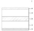
도 1은 종래의 발광 소자의 단면도이다.1 is a cross-sectional view of a conventional light emitting device.
발광 소자(1)는 n형 반도체층(10), 활성층(20) 및 p형 반도체층(30)을 포함한다. n형 반도체층(10) 측에는 n형 전극(50)이, p형 반도체층(30) 측에는 p형 전극(40)이 형성되어 있어 전압 등의 인가를 위하여 외부전원과 전기적으로 연결되어 있다.The
전극을 통하여 발광 소자(1)에 전압이 인가되면, n형 반도체층(10)으로부터 전자가 이동하고, p형 반도체층(30)으로부터 정공이 이동하여 전자 및 정공의 재결합을 통하여 발광이 일어난다. 도 1에 따른 발광 소자(1)는 활성층(20)을 포함하고, 발광은 활성층(20)에서 발생한다. 활성층(20)에서는 발광 소자(1)의 발광이 활성화된다.When a voltage is applied to the
n형 반도체층(10) 및 p형 반도체층(30)은 예를 들면, GaN계 반도체, ZnO계 반도체와 같은 무기 반도체를 포함한다. 각 반도체층(10, 30)은 각각의 타입에 따라 도핑되어 있다.The n-
그러나, 이러한 p-n 접합 형태의 무기반도체층을 갖는 발광 소자는 제작 과정이 어렵고, 단일 파장의 광을 방출하므로 백색광과 같이 다색이 요구되는 광소자에 사용할 경우에는 형광체와 같은 추가적인 요소가 필요한 단점이 있다.However, such a light emitting device having an inorganic semiconductor layer in the form of a pn junction is difficult to fabricate and emits light of a single wavelength, so that it is disadvantageous in that an additional element such as a phosphor is required when it is used in an optical device requiring multiple colors such as white light .
따라서, 실시예는 무기 반도체층과 유기 반도체층을 접합한 발광 소자를 제공하여, 기존의 무기 반도체의 p-n 접합과 같은 정류특성을 얻음과 동시에 제작이 간단하고 우수한 광학적 특성을 얻을 수 있는 발광 소자 및 이를 갖는 발광 소자 패키지를 제공하고자 함에 목적이 있다.Therefore, it is an object of the present invention to provide a light emitting device in which an inorganic semiconductor layer and an organic semiconductor layer are bonded to each other, to obtain rectifying characteristics such as pn junctions of existing inorganic semiconductors, And an object of the present invention is to provide a light emitting device package having such a structure.
실시예의 발광소자는, 기판; 상기 기판 상에 제1 무기반도체층; 상기 제1 무기반도체층 상에 배치되고, 광을 생성하는 활성층; 및 상기 활성층 상에 배치되고, 상기 활성층이 방출하는 광과 상이한 파장을 갖는 광을 생성하는 제2 유기반도체층; 을 포함한다.The light emitting device of the embodiment includes: a substrate; A first inorganic semiconductor layer on the substrate; An active layer disposed on the first inorganic semiconductor layer and generating light; And a second organic semiconductor layer disposed on the active layer, the second organic semiconductor layer generating light having a wavelength different from that of the light emitted from the active layer; .
또한, 상기 활성층과 상기 제2 유기반도체층 사이에 제2 무기반도체층; 을 더 포함한다.A second inorganic semiconductor layer between the active layer and the second organic semiconductor layer; .
또한, 상기 활성층과 상기 제2 유기반도체층 사이에 광을 방출하는 제1 유기반도체층; 을 더 포함한다.A first organic semiconductor layer that emits light between the active layer and the second organic semiconductor layer; .
또한, 상기 활성층, 상기 제1 유기반도체층 및 상기 제2 유기반도체층은 각각 다른 파장 영역의 광을 방출한다.In addition, the active layer, the first organic semiconductor layer, and the second organic semiconductor layer emit light in different wavelength regions, respectively.
또한, 상기 제1 유기반도체층의 LUMO 및 HOMO 에너지 준위는 각각 상기 활성층의 전도대 및 가전자대의 에너지보다 높고, 상기 제2 유기반도체층의 LUMO 및 HOMO 에너지 준위는 각각 상기 제1 유기반도체층의 LUMO 및 HOMO 에너지 준위보다 높다.The LUMO and HOMO energy levels of the first organic semiconductor layer are higher than the energy of the conduction band and the valence band of the active layer, respectively, and the LUMO and HOMO energy levels of the second organic semiconductor layer are LUMO And the HOMO energy level.
또한, 상기 제1 무기반도체층은 n형 반도체이고, 상기 제2 유기반도체층은 p형 반도체이다.The first inorganic semiconductor layer is an n-type semiconductor, and the second organic semiconductor layer is a p-type semiconductor.
또한, 상기 활성층과 상기 제2 유기반도체층 사이에 p형의 제1 유기반도체층; 을 더 포함한다.A p-type first organic semiconductor layer between the active layer and the second organic semiconductor layer; .
또한, 상기 제2 유기반도체층은 2이상의 서로 다른 유기물질이 혼합되어 이루어진다.Also, the second organic semiconductor layer is formed by mixing two or more different organic materials.
또한, 상기 제2 유기반도체층은 2 이상의 서로 다른 파장의 광을 방출한다.In addition, the second organic semiconductor layer emits light having two or more different wavelengths.
또한, 상기 제1 무기반도체층은 박막 혹은 양자점이나 선형태의 나노구조를 갖는다.Further, the first inorganic semiconductor layer has a thin film, a quantum dot, or a nanostructure of a line shape.
다른 실시예의 발광소자는, 기판; 상기 기판 상에 제1 무기반도체층; 및 상기 제1 무기반도체층 상에 형성되고, 광을 생성하는 제2 유기반도체층; 을 포함한다.A light emitting device of another embodiment includes: a substrate; A first inorganic semiconductor layer on the substrate; A second organic semiconductor layer formed on the first inorganic semiconductor layer and generating light; .
또한, 상기 제1 무기반도체층은 상기 제2 유기반도체층이 생성하는 광의 파장과는 상이한 파장을 갖는다.The first inorganic semiconductor layer has a wavelength different from a wavelength of light generated by the second organic semiconductor layer.
또한, 상기 제1 무기반도체층과 상기 제2 유기반도체층 사이에 제2 무기반도체층; 을 더 포함한다.A second inorganic semiconductor layer between the first inorganic semiconductor layer and the second organic semiconductor layer; .
또한, 상기 제1 무기반도체층과 상기 제2 유기반도체층 사이에 광을 방출하는 제1 유기반도체층; 을 더 포함한다.A first organic semiconductor layer that emits light between the first inorganic semiconductor layer and the second organic semiconductor layer; .
또한, 상기 제1 무기반도체층, 상기 제1 유기반도체층 및 상기 제2 유기반도체층은 각각 다른 파장 영역의 광을 방출한다.Further, the first inorganic semiconductor layer, the first organic semiconductor layer, and the second organic semiconductor layer emit light in different wavelength regions, respectively.
또한, 상기 제1 유기반도체층의 LUMO 및 HOMO 에너지 준위는 각각 상기 제1 무기반도체층의 전도대 및 가전자대의 에너지보다 높고, 상기 제2 유기반도체층의 LUMO 및 HOMO 에너지 준위는 각각 상기 제1 유기반도체층의 LUMO 및 HOMO 에너지 준위보다 높다.The LUMO and HOMO energy levels of the first organic semiconductor layer are higher than those of the conduction band and the valence band of the first inorganic semiconductor layer, respectively, and the LUMO and HOMO energy levels of the second organic semiconductor layer are higher than the energy of the first organic semiconductor layer. Is higher than the LUMO and HOMO energy levels of the semiconductor layer.
또한, 상기 제1 무기반도체층은 n형 반도체이고, 상기 제2 유기반도체층은 p형 반도체이다.The first inorganic semiconductor layer is an n-type semiconductor, and the second organic semiconductor layer is a p-type semiconductor.
또한, 상기 제1 무기반도체층과 상기 제2 유기반도체층 사이에 p형의 제1 유기반도체층; 을 더 포함한다.A p-type first organic semiconductor layer between the first inorganic semiconductor layer and the second organic semiconductor layer; .
또한, 상기 제1 및 제2 유기반도체층은 2 이상의 서로 다른 유기물질이 혼합되어 이루어질 수 있다.In addition, the first and second organic semiconductor layers may be formed by mixing two or more different organic materials.
또한, 혼합된 유기반도체층은 2 이상의 서로 다른 파장의 광을 방출한다.Further, the mixed organic semiconductor layer emits light of two or more different wavelengths.
실시예의 발광 소자 패키지는, 패키지 몸체; 상기 패키지 몸체 상에 구비되는 제1항 내지 제23항 중 어느 한 항에 따른 발광 소자; 상기 패키지 몸체에 구비되고, 상기 발광 소자와 각각 연결되는 제1 전극층과 제2 전극층; 및 상기 발광 소자를 포위하는 충진재; 를 포함한다.A light emitting device package of an embodiment includes: a package body; A light emitting device according to any one of
실시예는 무기 반도체층과 유기 반도체층을 접합한 발광 소자를 제공함으로써, 기존의 무기 반도체의 p-n 접합과 같은 정류특성을 얻음과 동시에 제작이 간단하고 우수한 광학적 특성을 얻을 수 있는 발광 소자 및 이를 갖는 발광 소자 패키지를 제공할 수 있다.The present embodiment provides a light emitting device in which a rectifying characteristic such as a pn junction of a conventional inorganic semiconductor is obtained by providing a light emitting device in which an inorganic semiconductor layer and an organic semiconductor layer are bonded to each other, The light emitting device package can be provided.
도 1은 종래의 발광 소자의 단면도이다.
도 2는 본 발명의 제1 실시예에 따른 반도체 발광 소자의 단면도이다.
도 3은 기존의 질화물 발광 소자와 본 발명의 실시예의 이종접합 발광 소자의 발광 특성을 나타내는 도면이다.
도 4는 본 발명의 제2 실시예에 따른 반도체 발광 소자의 단면도이다.
도 5는 본 발명의 제2 실시예에 따른 반도체 발광 소자의 에너지 밴드 다이어그램이다.
도 6은 본 발명의 제3 실시예에 따른 반도체 발광 소자의 단면도이다.
도 7은 본 발명의 실시예에 따른 수직구조의 반도체 발광 소자를 도시하는 단면도이다.
도 8은 본 발명의 발광 소자 패키지의 일실시예의 단면도이다.1 is a cross-sectional view of a conventional light emitting device.
2 is a cross-sectional view of a semiconductor light emitting device according to a first embodiment of the present invention.
FIG. 3 is a diagram showing light emission characteristics of a conventional nitride light emitting device and a heterojunction light emitting device of an embodiment of the present invention.
4 is a cross-sectional view of a semiconductor light emitting device according to a second embodiment of the present invention.
5 is an energy band diagram of a semiconductor light emitting device according to a second embodiment of the present invention.
6 is a cross-sectional view of a semiconductor light emitting device according to a third embodiment of the present invention.
7 is a cross-sectional view illustrating a semiconductor light emitting device having a vertical structure according to an embodiment of the present invention.
8 is a cross-sectional view of one embodiment of the light emitting device package of the present invention.
이하 상기의 목적을 구체적으로 실현할 수 있는 본 발명의 바람직한 실시예를 첨부한 도면을 참조하여 설명한다.DETAILED DESCRIPTION OF THE PREFERRED EMBODIMENTS Hereinafter, preferred embodiments of the present invention will be described with reference to the accompanying drawings.
상기의 실시예들의 설명에 있어서, 각 층(막), 영역, 패턴 또는 구조물들이 기판, 각 층(막), 영역, 패드 또는 패턴들의 "위(on)"에 또는 "아래(under)"에 형성되는 것으로 기재되는 경우에 있어, "위(on)"와 "아래(under)"는 "직접(directly)" 또는 "다른 층을 개재하여 (indirectly)" 형성되는 것을 모두 포함한다. 또한 각 층의 위 또는 아래에 대한 기준은 도면을 기준으로 설명한다.In describing the above embodiments, it is to be understood that each layer (film), area, pattern or structure may be referred to as being "on" or "under" the substrate, each layer Quot; on "and " under" include both being formed "directly" or "indirectly" In addition, the criteria for above or below each layer will be described with reference to the drawings.
도면에서 각층의 두께나 크기는 설명의 편의 및 명확성을 위하여 과장되거나 생략되거나 또는 개략적으로 도시되었다. 또한 각 구성요소의 크기는 실제크기를 전적으로 반영하는 것은 아니다.The thickness and size of each layer in the drawings are exaggerated, omitted, or schematically shown for convenience and clarity of explanation. Also, the size of each component does not entirely reflect the actual size.
실시예Example 1 One
도 2는 본 발명의 제1 실시예에 따른 반도체 발광 소자의 단면도로서, 수평구조의 반도체 발광 소자를 예시한 것이다. 도 3은 기존의 질화물 발광 소자와 본 발명의 실시예의 이종접합 발광 소자의 발광 특성을 나타내는 도면이다. 이하에서, 도 2 및 도 3을 참조하여 본 발명의 반도체 발광 소자의 일 실시예를 설명하기로 한다.2 is a cross-sectional view of a semiconductor light emitting device according to a first embodiment of the present invention, which illustrates a semiconductor light emitting device having a horizontal structure. FIG. 3 is a diagram showing light emission characteristics of a conventional nitride light emitting device and a heterojunction light emitting device of an embodiment of the present invention. Hereinafter, an embodiment of the semiconductor light emitting device of the present invention will be described with reference to FIGS. 2 and 3. FIG.
도 2에 도시한 바와 같이, 반도체 발광 소자는, 기판(110)과, 상기 기판(110) 상에 순차적으로 형성된 제1 무기반도체층(120), 활성층(130) 및 제2 유기반도체층(140)을 포함한다.2, the semiconductor light emitting device includes a substrate 110, a first inorganic semiconductor layer 120, an active layer 130, and a second organic semiconductor layer 140 sequentially formed on the substrate 110 ).
기판(110)은, 투광성을 갖는 재질, 예를 들어, 사파이어(Al203), GaN, SiC, ZnO, Si, GaP, InP, Ga203, 그리고 GaAs 등이 사용될 수 있다.For example, sapphire (Al2 O3 ), GaN, SiC, ZnO, Si, GaP, InP, Ga2 O3 , and GaAs may be used as the substrate 110.
기판(110) 상에는 제1 무기반도체층(120)이 형성된다. 제1 무기반도체층(120)은 상기 제1 무기반도체층(120) 아래에 언도프트 반도체층을 더 포함할 수 있으며, 이에 대해 한정하지는 않는다. 언도프트 반도체층은 제1 무기반도체층(120)의 결정성 향상을 위해 형성되는 층으로, n형 도펀트가 도핑되지 않아 제1 무기반도체층(120)에 비해 현저히 낮은 전기전도성을 갖는 것을 제외하고는, 제1 무기반도체층(120)과 같을 수 있다.The first inorganic semiconductor layer 120 is formed on the substrate 110. The first inorganic semiconductor layer 120 may further include an undoped semiconductor layer below the first inorganic semiconductor layer 120, but the present invention is not limited thereto. The un-doped semiconductor layer is a layer formed for improving the crystallinity of the first inorganic semiconductor layer 120, except that the n-type dopant is not doped and has a significantly lower electrical conductivity than the first inorganic semiconductor layer 120 May be the same as the first inorganic semiconductor layer 120.
제1 무기반도체층(120)은 질화물 반도체 또는 산화물 반도체 재료로 형성될 수 있고, Si, Ge, Sn, Se, Te 등의 n형 도펀트가 도핑될 수 있다. 예를 들어, 제1 무기반도체층(120)은 n형 도펀트가 도핑된 GaN, InAlGaN 또는 ZnO로 이루어질 수 있다. 제1 무기반도체층(120)은 박막 형태가 아닌 나노 구조, 예를 들어 나노와이어(nanowire), 나노막대(nanorod) 등으로 형성될 수 있다.The first inorganic semiconductor layer 120 may be formed of a nitride semiconductor or an oxide semiconductor material and may be doped with an n-type dopant such as Si, Ge, Sn, Se or Te. For example, the first inorganic semiconductor layer 120 may be composed of GaN, InAlGaN, or ZnO doped with an n-type dopant. The first inorganic semiconductor layer 120 may be formed of a nanostructure other than a thin film, for example, a nanowire, a nanorod, or the like.
제1 무기반도체층(120) 상에는 활성층(130)이 형성된다. 활성층(130)은 예를 들어, InxAlyGa1-x-yN의 조성식(여기서, 0≤x≤1, 0≤y≤1, 0≤x+y≤1임)을 갖는 반도체 재료를 포함하여 형성할 수 있으며, 양자선(Quantum wire) 구조, 양자점(Quantum dot) 구조, 단일양자우물 구조 또는 다중양자우물 구조(Multi Quantum Well; MQW) 중 적어도 하나를 포함할 수 있다. 예를 들어, 활성층(130)은 다중양자우물 구조의 InGaN/GaN층으로 이루어질 수 있다.The active layer 130 is formed on the first inorganic semiconductor layer 120. The active layer 130 is formed of a semiconductor material having a composition formula of Inx Aly Ga1-x-y N (where 0?X? 1, 0?Y? 1, 0?X + y? 1) And may include at least one of a quantum wire structure, a quantum dot structure, a single quantum well structure or a multi quantum well structure (MQW). For example, the active layer 130 may be formed of an InGaN / GaN layer having a multiple quantum well structure.
활성층(130)은 제1 무기반도체층(120) 및 제2 유기반도체층(140)으로부터 제공되는 전자 및 정공의 재결합(recombination) 과정에서 발생되는 에너지에 의해 광을 방출한다.The active layer 130 emits light by energy generated during the recombination of electrons and holes provided from the first inorganic semiconductor layer 120 and the second organic semiconductor layer 140.
활성층(130) 상에는 제2 유기반도체층(140)이 형성된다. 제2 유기반도체층(140)은 저분자계나 고분자 계열을 이용하여 열증착법(Thermal Evaporation) 또는 액체에 용해된 상태에서 스핀 코팅법(Spin Coating)을 통해 제작될 수 있다. 제2 유기반도체층(140)은 예를 들어 N,N'-diphenyl-N,N'-bis(1-naphthyl)-1,1'-bisphenyl-4,4'-diamine(α-NPD)로 형성될 수 있고, p형 도펀트 역할을 하는 물질이 도핑될 수 있다.A second organic semiconductor layer 140 is formed on the active layer 130. The second organic semiconductor layer 140 may be formed by a thermal evaporation method using a low molecular material or a polymer material or by a spin coating method while being dissolved in a liquid. The second organic semiconductor layer 140 may be formed of, for example, N, N'-diphenyl-N, N'-bis (1-naphthyl) -1,1'-bisphenyl-4,4'- And a material that serves as a p-type dopant can be doped.
제2 유기반도체층(140) 상에는 p형 전극(150)이 형성된다. 한편, 제2 유기반도체층(140), 활성층(130)의 일부는 식각(etching)으로 제거되어, 저면에 제1 무기반도체층(120)의 일부를 드러내고 있다. 식각에 의해 드러난 제1 무기반도체층(120), 즉 활성층(130)이 형성되지 않은 제1 무기반도체층(120) 상에는 n형 전극(160)이 형성되어 있다.A p-type electrode 150 is formed on the second organic semiconductor layer 140. On the other hand, a part of the second organic semiconductor layer 140 and the active layer 130 is removed by etching, and a part of the first inorganic semiconductor layer 120 is exposed on the bottom surface. The n-type electrode 160 is formed on the first inorganic semiconductor layer 120, that is, the first inorganic semiconductor layer 120 on which the active layer 130 is not formed.
상기에서 제1 무기반도체층(120)은 n형 반도체로 형성되고, 제2 유기반도체층(140)은 p형 반도체로 형성되는 것으로 설명하였지만, 반대로 제1 무기반도체층(120)이 p형 반도체로 형성되고, 제2 유기반도체층(140)이 n형 반도체로 형성될 수도 있다.Although the first inorganic semiconductor layer 120 is formed of an n-type semiconductor and the second organic semiconductor layer 140 is formed of a p-type semiconductor, the first inorganic semiconductor layer 120 may be a p- And the second organic semiconductor layer 140 may be formed of an n-type semiconductor.
제2 유기반도체층(140)은 발광 재료로 형성되어, 제1 무기반도체층(120) 및 제2 유기반도체층(140)으로부터 제공되는 전자 및 정공의 재결합과정에서 발생되는 에너지에 의해 광을 방출한다.The second organic semiconductor layer 140 is formed of a light emitting material and emits light by energy generated in the recombination process of electrons and holes provided from the first inorganic semiconductor layer 120 and the second organic semiconductor layer 140 do.
제2 유기반도체층(140)의 LUMO(Lowest Unoccupied Molecular Orbital; 가장 낮은 비점유된 분자궤도함수) 및 HOMO(Highest Occupied Molecular Orbital; 가장 높은 점유된 분자궤도함수)의 에너지 준위는 각각 활성층(130)의 전도대(conduction band) 및 가전자대(valence band)의 에너지보다 높아, 기존의 무기 p-n 접합 구조와 유사한 밴드구조를 갖는 것이 바람직하다.The energy levels of the LUMO (Lowest Unoccupied Molecular Orbital) and the HOMO (High Occupied Molecular Orbital) of the second organic semiconductor layer 140 are respectively set to the active layer 130, Is higher than the energy of the conduction band and the valence band of the conventional inorganic pn junction structure.
도 3을 참조하면, 기존의 질화물 발광 소자는 단일 파장의 광을 방출하지만, 본 발명의 실시예의 유기/무기 이종접합 발광 소자는 2 이상의 다른 파장의 광을 방출함을 확인할 수 있다.Referring to FIG. 3, it can be confirmed that the conventional nitride light emitting device emits light of a single wavelength, but the organic / inorganic heterojunction light emitting device of the present invention emits light of two or more different wavelengths.
본 실시예의 유기/무기 이종접합 발광 소자는 백색광과 같이 다색이 요구되는 광소자에 매우 유용하게 적용될 수 있다. 즉, 활성층(130)과 제2 유기반도체층(140)에서 서로 다른 파장의 광을 방출하도록, 예를 들어 활성층(130)에서 청색 광을 방출하고, 제2 유기반도체층(140)에서 황색 광을 방출하도록 구성함으로써, 백색광을 구현할 수 있다.The organic / inorganic heterojunction light emitting device of the present embodiment can be very usefully applied to an optical device requiring multiple colors such as white light. That is, for example, blue light is emitted from the active layer 130 and blue light is emitted from the second organic semiconductor layer 140 to emit light of different wavelengths in the active layer 130 and the second organic semiconductor layer 140, So that white light can be realized.
이와 같이, 실시예의 발광 소자는 활성층(130)과 제2 유기반도체층(140)이 모두 발광층으로서의 역할을 하므로, 원하는 에너지 대역(에너지 밴드갭)을 갖는 물질들을 조합하여 색을 조절할 수 있다.Thus, since the active layer 130 and the second organic semiconductor layer 140 both function as a light emitting layer, the light emitting device of the embodiment can control the color by combining materials having a desired energy band (energy band gap).
또한, 실시예의 제2 유기반도체층(140)은 서로 다른 종류의 유기물질을 혼합하여 형성될 수 있다. 이러한 경우, 제2 유기반도체층(140)은 각각의 유기물질에서 발광이 일어나서 2 이상의 서로 다른 파장의 광을 방출함으로써, 활성층(130)과 함께 3 파장 대역 이상의 다색발광소자를 얻을 수 있다.In addition, the second organic semiconductor layer 140 may be formed by mixing different kinds of organic materials. In this case, the second organic semiconductor layer 140 emits light in each organic material and emits light having two or more different wavelengths, so that a multicolor light emitting device having a wavelength band of three wavelengths or more can be obtained together with the active layer 130.
실시예의 발광 소자는 유기/무기 이종접합으로 이루어지지만, 기존의 무기 p-n 접합 다이오드와 마찬가지로 우수한 정류 특성을 보인다.The light emitting device of the embodiment is made of an organic / inorganic heterojunction, but exhibits excellent rectifying characteristics as in the conventional inorganic p-n junction diode.
또한, 실시예의 제2 유기반도체층(140)은 기존의 무기반도체층과 비교하여 제작과정이 쉽고, 낮은 온도 영역에서 제작될 수 있기 때문에, 저가, 대면적 소자로서 매우 유용한 장점을 갖고 있다.In addition, since the second organic semiconductor layer 140 of the embodiment is easy to manufacture and can be manufactured in a low temperature region as compared with the conventional inorganic semiconductor layer, it is very advantageous as a low-cost, large-area element.
본 실시예의 발광 소자에서, 제1 무기반도체층(120)과 제2 유기반도체층(140) 사이에 활성층(130)이 포함되지 않고, 제1 무기반도체층(120) 위에 제2 유기반도체층(140)이 형성되는 것도 가능하다. 이러한 경우, 제1 무기반도체층(120)이 발광층으로서의 역할을 하게 되고, 마찬가지의 효과를 가지게 된다.The active layer 130 is not included between the first inorganic semiconductor layer 120 and the second organic semiconductor layer 140 and the second organic semiconductor layer 140 may be formed. In this case, the first inorganic semiconductor layer 120 serves as a light emitting layer, and the same effect can be obtained.
실시예Example 2 2
도 4는 본 발명의 제2 실시예에 따른 반도체 발광 소자의 단면도로서, 수평구조의 반도체 발광 소자를 예시한 것이다. 도 5는 본 발명의 제2 실시예에 따른 반도체 발광 소자의 에너지 밴드 다이어그램이다. 이하에서, 도 4 및 도 5를 참조하여 본 발명의 반도체 발광 소자의 제2 실시예를 설명하기로 한다.4 is a cross-sectional view of a semiconductor light emitting device according to a second embodiment of the present invention, which illustrates a semiconductor light emitting device having a horizontal structure. 5 is an energy band diagram of a semiconductor light emitting device according to a second embodiment of the present invention. Hereinafter, a second embodiment of the semiconductor light emitting device of the present invention will be described with reference to FIGS. 4 and 5. FIG.
도 4를 참조하면, 반도체 발광 소자는, 기판(210)과, 상기 기판(210) 상에 순차적으로 형성된 제1 무기반도체층(220), 활성층(230), 제1 유기반도체층(240) 및 제2 유기반도체층(250)을 포함한다.4, the semiconductor light emitting device includes a
본 실시예의 기판(210), 제1 무기반도체층(220), 활성층(230) 및 제2 유기반도체층(250)은 상술한 제1 실시예의 기판(110), 제1 무기반도체층(120), 활성층(130) 및 제2 유기반도체층(140)과 유사한 구성을 갖는다. 또한, n형 전극(260) 및 p형 전극(270)도 제1 실시예의 n형 전극(150) 및 p형 전극(160)과 유사한 구성을 갖는다.The
본 실시예에서는 활성층(230)과 제2 유기반도체층(250) 사이에 제1 유기반도체층(240)이 구비되어 있다.In this embodiment, a first
제1 유기반도체층(240)은 저분자계나 고분자 계열을 이용하여 열증착법(Thermal Evaporation) 또는 액체에 용해된 상태에서 스핀 코팅법(Spin Coating)을 통해 제작될 수 있다. 제1 유기반도체층(240)은 예를 들어, Poly(N-vinylcarbazole)(PVK)로 형성될 수 있고, p형 도펀트 역할을 하는 물질이 도핑될 수 있다.The first
제1 유기반도체층(240)은 발광 재료로 형성되어, 제1 무기반도체층(220) 및 제1 유기반도체층(240)으로부터 제공되는 전자 및 정공의 재결합과정에서 발생되는 에너지에 의해 광을 방출한다.The first
마찬가지로, 제2 유기반도체층(250)도 제1 무기반도체층(220) 및 제2 유기반도체층(250)으로부터 제공되는 전자 및 정공의 재결합과정에서 발생되는 에너지에 의해 광을 방출한다.Similarly, the second
도 5에 도시된 바와 같이, 제1 유기반도체층(240)의 LUMO 및 HOMO의 에너지 준위는 각각 활성층(230)의 전도대 및 가전자대의 에너지보다 높은 것이 바람직하다. 또한, 제2 유기반도체층(250)의 LUMO 및 HOMO의 에너지 준위는 각각 제1 유기반도체층(240)의 LUMO 및 HOMO의 에너지 준위보다 높은 것이 바람직하다. 이는 이종접합된 활성층(230), 제1 유기반도체층(240), 제2 유기반도체층(250) 사이의 전도대와 LUMO, 가전자대와 HOMO 사이의 에너지 갭이 줄어들게 하여, 유기/무기 반도체 간의 전하이동을 원활하게 하고 발광효율이 높아지게 한다.5, the energy levels of LUMO and HOMO of the first
본 실시예의 발광 소자는 활성층(230), 제1 유기반도체층(240) 및 제2 유기반도체층(250)이 모두 발광층으로서의 역할을 하므로, 원하는 에너지 대역(에너지 밴드갭)을 갖는 물질들을 조합하여 발광색을 조절할 수 있다. 예를 들어, 활성층(130)에서 청색 광을 방출하고, 제1 유기반도체층(240)에서 녹색 광을 방출하고, 제2 유기반도체층(250)에서 적색 광을 방출하도록 구성함으로써, 백색광을 구현할 수 있다. 또한, 발광 소자는 백색광 이외의 다양한 다색발광소자를 구현할 수 있다.Since the
제1 무기반도체층(220)은 n형 반도체로 형성되고, 제1 유기반도체층(240) 및 제2 유기반도체층(250)은 p형 반도체로 형성되지만, 반대로 제1 무기반도체층(220)이 p형 반도체로 형성되고, 제1 유기반도체층(240) 및 제2 유기반도체층(250)이 n형 반도체로 형성될 수도 있다.The first
본 실시예의 발광 소자에서, 제1 무기반도체층(220)과 제1 유기반도체층(240) 사이에 활성층(230)이 포함되지 않고, 제1 무기반도체층(220) 위에 제1 유기반도체층(240)이 형성되는 것도 가능하다. 이러한 경우, 제1 무기반도체층(220)이 발광층으로서의 역할을 하게 되고, 마찬가지의 효과를 가지게 된다.The
실시예Example 3 3
도 6은 본 발명의 제3 실시예에 따른 반도체 발광 소자의 단면도로서, 수평구조의 반도체 발광 소자를 예시한 것이다.6 is a cross-sectional view of a semiconductor light emitting device according to a third embodiment of the present invention, which illustrates a semiconductor light emitting device having a horizontal structure.
도 6을 참조하면, 반도체 발광 소자는, 기판(310)과, 상기 기판(310) 상에 순차적으로 형성된 제1 무기반도체층(320), 활성층(330), 제2 무기반도체층(340) 및 제2 유기반도체층(350)을 포함한다.6, the semiconductor light emitting device includes a
본 실시예의 기판(310), 제1 무기반도체층(320), 활성층(330) 및 제2 유기반도체층(350)은 상술한 제1 실시예의 기판(110), 제1 무기반도체층(120), 활성층(130) 및 제2 유기반도체층(140)과 유사한 구성을 갖는다. 또한, n형 전극(360) 및 p형 전극(370)도 제1 실시예의 n형 전극(150) 및 p형 전극(160)과 유사한 구성을 갖는다.The
본 실시예에서는 활성층(330)과 제2 유기반도체층(350) 사이에 제2 무기반도체층(340)이 구비되어 있다.In this embodiment, a second
제2 무기반도체층(340)은 질화물 반도체 또는 산화물 반도체 재료로 형성될 수 있고, Si, Ge, Sn, Se, Te 등의 n형 도펀트가 도핑될 수 있다. 예를 들어, 제2 무기반도체층(340)은 n형 도펀트가 도핑된 GaN, InAlGaN 또는 ZnO로 이루어질 수 있다. 제2 무기반도체층(340)은 박막 형태가 아닌 나노 구조, 예를 들어 나노와이어(nanowire), 나노막대(nanorod) 등으로 형성될 수 있다.The second
본 실시예에서는 제1 실시예에서와 마찬가지로 활성층(330)과 제2 유기반도체층(350)이 모두 발광층으로서의 역할을 하므로, 원하는 에너지 대역(에너지 밴드갭)을 갖는 물질들을 조합하여 색을 조절할 수 있다. 즉, 활성층(330)과 제2 유기반도체층(350)에서 서로 다른 파장의 광을 방출하도록 구성함으로써, 백색광 또는 다색발광소자를 구현할 수 있다.In this embodiment, since the
본 실시예의 발광 소자에서, 제1 무기반도체층(320)과 제2 무기반도체층(340) 사이에 활성층(330)이 포함되지 않고, 제1 무기반도체층(320) 위에 제2 무기반도체층(340)이 형성되는 것도 가능하다. 이러한 경우, 제1 무기반도체층(320) 또는 제2 무기반도체층(340)이 발광층으로서의 역할을 하게 되고, 마찬가지의 효과를 가지게 된다.The
수직구조의 발광 소자Vertical structure light emitting element
도 7은 본 발명의 실시예에 따른 수직구조의 반도체 발광 소자를 도시하는 단면도이다.7 is a cross-sectional view illustrating a semiconductor light emitting device having a vertical structure according to an embodiment of the present invention.
도시한 바와 같이, 반도체 발광 소자의 최하부에는 구조지지층(410)이 형성되어 있다. 구조지지층(410)은, 발광 소자의 지지층 및 전극으로서의 역할을 수행하는 것으로서, 실리콘(Si) 기판, GaAs 기판, Ge 기판 또는 금속층 등으로 이루어질 수 있다.As shown in the figure, a
구조지지층(410) 상에는 p형 전극(460)이 형성되어 있으며, 이는 전극 역할 및 반사 역할을 동시에 하도록 반사율이 높은 금속으로 이루어지는 것이 바람직하다.A p-
p형 전극(460) 상에는 제2 유기반도체층(440), 활성층(430) 및 제1 무기반도체층(420)이 순차로 형성되어 있고, 제1 무기반도체층(420) 상에는 n형 전극(450)이 형성되어 있다.A second
제2 유기반도체층(440)은 저분자계나 고분자 계열을 이용하여 열증착법(Thermal Evaporation) 또는 액체에 용해된 상태에서 스핀 코팅법(Spin Coating)을 통해 제작될 수 있다. 제2 유기반도체층(440)은 예를 들어 N,N'-diphenyl-N,N'-bis(1-naphthyl)-1,1'-bisphenyl-4,4'-diamine(α-NPD)로 형성될 수 있고, p형 도펀트 역할을 하는 물질이 도핑될 수 있다.The second
제2 유기반도체층(440)은 발광 재료로 형성되어, 제1 무기반도체층(420) 및 제2 유기반도체층(440)으로부터 제공되는 전자 및 정공의 재결합과정에서 발생되는 에너지에 의해 광을 방출한다.The second
제2 유기반도체층(440) 상에는 활성층(430)이 형성된다. 활성층(130)은 예를 들어, InxAlyGa1-x-yN의 조성식(여기서, 0≤x≤1, 0≤y≤1, 0≤x+y≤1임)을 갖는 반도체 재료를 포함하여 형성할 수 있으며, 양자선(Quantum wire) 구조, 양자점(Quantum dot) 구조, 단일양자우물 구조 또는 다중양자우물 구조(Multi Quantum Well; MQW) 중 적어도 하나를 포함할 수 있다. 예를 들어, 활성층(130)은 다중양자우물 구조의 InGaN/GaN층으로 이루어질 수 있다. 활성층(430)은 제1 무기반도체층(420) 및 제2 유기반도체층(440)으로부터 제공되는 전자 및 정공의 재결합 과정에서 발생되는 에너지에 의해 광을 방출한다.An
활성층(430) 상에는 제1 무기반도체층(420)이 형성된다. 제1 무기반도체층(420)은 질화물 반도체 또는 산화물 반도체 재료로 형성될 수 있고, Si, Ge, Sn, Se, Te 등의 n형 도펀트가 도핑될 수 있다. 예를 들어, 제1 무기반도체층(420)은 n형 도펀트가 도핑된 N, GaN, InAlGaN 또는 ZnO로 이루어질 수 있다. 제1 무기반도체층(420)은 박막 형태가 아닌 나노 구조, 예를 들어 나노와이어(nanowire), 나노막대(nanorod) 등으로 형성될 수 있다.A first
상기에서 제1 무기반도체층(420)은 n형 반도체로 형성되고, 제2 유기반도체층(440)은 p형 반도체로 형성되는 것으로 설명하였지만, 반대로 제1 무기반도체층(420)이 p형 반도체로 형성되고, 제2 유기반도체층(440)이 n형 반도체로 형성될 수도 있다.Although the first
본 실시예의 유기/무기 이종접합 발광 소자는 수직구조라는 것을 제외하고는 수평구조의 반도체 발광 소자를 예시한 제1, 제2 및 제3 실시예의 반도체 발광 소자의 구성을 모두 포함할 수 있고, 그에 따른 효과도 동일함을 알 수 있다.The organic / inorganic heterojunction light emitting device of this embodiment may include all of the configurations of the semiconductor light emitting devices of the first, second, and third embodiments, which are exemplified as a horizontal semiconductor light emitting device, The same effect is also obtained.
발광 소자 패키지The light-
도 8은 본 발명의 발광 소자 패키지의 일실시예의 단면도이다. 이하에서, 도 8을 참조하여 발광 소자 패키지의 일실시예를 설명한다.8 is a cross-sectional view of one embodiment of the light emitting device package of the present invention. Hereinafter, an embodiment of the light emitting device package will be described with reference to FIG.
도시된 바와 같이, 실시예에 따른 발광 소자 패키지는 패키지 몸체(510)와, 패키지 몸체(510)에 형성된 제 1 전극층(521) 및 제 2 전극층(522)과, 패키지 몸체(510)에 설치되어 제 1 전극층(521) 및 제 2 전극층(522)과 전기적으로 연결되는 실시예에 따른 발광 소자(500)와, 이러한 발광 소자(500)를 포위하는 충진재(530)를 포함한다.As shown in the figure, the light emitting device package according to the embodiment includes a
패키지 몸체(510)는 실리콘 재질, 합성수지 재질, 또는 금속 재질을 포함하여 형성될 수 있으며, 발광 소자(500)의 주위에 경사면이 형성되어 광추출 효율을 높일 수 있다.The
제 1 전극층(521) 및 제 2 전극층(522)은 서로 전기적으로 분리되며, 발광 소자(500)에 전원을 제공한다. 또한, 제 1 전극층(521) 및 제 2 전극층(522)은 발광 소자(500)에서 발생된 광을 반사시켜 광 효율을 증가시킬 수 있으며, 발광 소자(500)에서 발생된 열을 외부로 배출시키는 역할을 할 수도 있다.The
발광 소자(500)는 패키지 몸체(510) 상에 설치되거나 제 1 전극층(521) 또는 제 2 전극층(522) 상에 설치된다.The
발광 소자(500)는 제 1 전극층(521) 및 제 2 전극층(522)과 와이어 방식, 플립칩 방식 또는 다이 본딩 방식 중 어느 하나에 의해 전기적으로 연결될 수 있다.The
충진재(530)는 발광 소자(500)를 포위하여 보호한다. 또한, 충진재(530)에는 형광체가 포함되어 발광 소자(500)에서 방출된 광의 파장을 변화시킬 수 있다.The
발광 소자 패키지는 상기에 개시된 실시예들의 발광 소자 중 적어도 하나를 하나 또는 복수개로 탑재할 수 있으며, 이에 대해 한정하지는 않는다.The light emitting device package may include at least one of the light emitting devices of the above-described embodiments, but may not be limited thereto.
실시 예에 따른 발광 소자 패키지는 복수개가 기판 상에 배열되며, 발광 소자 패키지의 광 경로 상에 광학 부재인 도광판, 프리즘 시트, 확산 시트 등이 배치될 수 있다. 이러한 발광 소자 패키지, 기판, 광학 부재는 라이트 유닛으로 기능할 수 있다. 또 다른 실시 예는 상술한 실시 예들에 기재된 반도체 발광 소자 또는 발광 소자 패키지를 포함하는 표시 장치, 지시 장치, 조명 시스템으로 구현될 수 있으며, 예를 들어, 조명 시스템은 램프, 가로등을 포함할 수 있다.A light guide plate, a prism sheet, a diffusion sheet, and the like, which are optical members, may be disposed on the light path of the light emitting device package. Such a light emitting device package, a substrate, and an optical member can function as a light unit. Still another embodiment may be implemented as a display device, an indicating device, a lighting system including the semiconductor light emitting device or the light emitting device package described in the above embodiments, for example, the lighting system may include a lamp, a streetlight .
이상에서 실시예들에 설명된 특징, 구조, 효과 등은 본 발명의 적어도 하나의 실시예에 포함되며, 반드시 하나의 실시예에만 한정되는 것은 아니다. 나아가, 각 실시예에서 예시된 특징, 구조, 효과 등은 실시예들이 속하는 분야의 통상의 지식을 가지는 자에 의해 다른 실시예들에 대해서도 조합 또는 변형되어 실시 가능하다. 따라서 이러한 조합과 변형에 관계된 내용들은 본 발명의 범위에 포함되는 것으로 해석되어야 할 것이다.The features, structures, effects and the like described in the embodiments are included in at least one embodiment of the present invention and are not necessarily limited to only one embodiment. Furthermore, the features, structures, effects and the like illustrated in the embodiments can be combined and modified by other persons skilled in the art to which the embodiments belong. Therefore, it should be understood that the present invention is not limited to these combinations and modifications.
또한, 이상에서 실시예를 중심으로 설명하였으나 이는 단지 예시일 뿐 본 발명을 한정하는 것이 아니며, 본 발명이 속하는 분야의 통상의 지식을 가진 자라면 본 실시예의 본질적인 특성을 벗어나지 않는 범위에서 이상에 예시되지 않은 여러 가지의 변형과 응용이 가능함을 알 수 있을 것이다. 예를 들어, 실시예에 구체적으로 나타난 각 구성 요소는 변형하여 실시할 수 있는 것이다. 그리고 이러한 변형과 응용에 관계된 차이점들은 첨부된 청구 범위에서 규정하는 본 발명의 범위에 포함되는 것으로 해석되어야 할 것이다.While the present invention has been particularly shown and described with reference to exemplary embodiments thereof, it is clearly understood that the same is by way of illustration and example only and is not to be taken by way of illustration, It can be seen that various modifications and applications are possible. For example, each component specifically shown in the embodiments can be modified and implemented. It is to be understood that all changes and modifications that come within the meaning and range of equivalency of the claims are therefore intended to be embraced therein.
1 : 발광 소자 10 : n형 반도체층
20 : 활성층 30 : 제2 유기반도체층
40 : n형 전극 50 : p형 전극
110 : 기판 120 : 제1 무기반도체층
130 : 활성층 140 : 제2 유기반도체층
150 : p형 전극 160 : n형 전극
510 : 패키지 몸체 521 : 제1 전극층
522 : 제2 전극층 530 : 충진재
500 : 발광 소자1: light emitting element 10: n-type semiconductor layer
20: active layer 30: second organic semiconductor layer
40: n-type electrode 50: p-type electrode
110: substrate 120: first inorganic semiconductor layer
130: active layer 140: second organic semiconductor layer
150: p-type electrode 160: n-type electrode
510: package body 521: first electrode layer
522: second electrode layer 530: filler
500: light emitting element
Claims (22)
Translated fromKorean상기 기판 상에 제1 무기반도체층;
상기 제1 무기반도체층 상에 배치되고, 광을 생성하는 활성층; 및
상기 활성층 상에 배치되고, 상기 활성층이 방출하는 광과 상이한 파장을 갖는 광을 생성하는 제2 유기반도체층;
을 포함하는 발광 소자.Board;
A first inorganic semiconductor layer on the substrate;
An active layer disposed on the first inorganic semiconductor layer and generating light; And
A second organic semiconductor layer disposed on the active layer and generating light having a wavelength different from that of the light emitted from the active layer;
.
상기 활성층과 상기 제2 유기반도체층 사이에 제2 무기반도체층;
을 더 포함하는 발광 소자.The method according to claim 1,
A second inorganic semiconductor layer between the active layer and the second organic semiconductor layer;
Emitting device.
상기 활성층과 상기 제2 유기반도체층 사이에 광을 방출하는 제1 유기반도체층;
을 더 포함하는 발광 소자.The method according to claim 1,
A first organic semiconductor layer that emits light between the active layer and the second organic semiconductor layer;
Emitting device.
상기 활성층, 상기 제1 유기반도체층 및 상기 제2 유기반도체층은 각각 다른 파장 영역의 광을 방출하는 발광 소자.The method of claim 3,
Wherein the active layer, the first organic semiconductor layer, and the second organic semiconductor layer emit light in different wavelength regions, respectively.
상기 제1 유기반도체층의 LUMO 및 HOMO 에너지 준위는 각각 상기 활성층의 전도대 및 가전자대의 에너지보다 높고,
상기 제2 유기반도체층의 LUMO 및 HOMO 에너지 준위는 각각 상기 제1 유기반도체층의 LUMO 및 HOMO 에너지 준위보다 높은 발광 소자.The method of claim 3,
The LUMO and HOMO energy levels of the first organic semiconductor layer are higher than the energy of the conduction band and the valence band of the active layer,
Wherein the LUMO and HOMO energy levels of the second organic semiconductor layer are higher than the LUMO and HOMO energy levels of the first organic semiconductor layer, respectively.
상기 제1 무기반도체층은 n형 반도체이고,
상기 제2 유기반도체층은 p형 반도체인 발광 소자.The method according to claim 1,
Wherein the first inorganic semiconductor layer is an n-type semiconductor,
And the second organic semiconductor layer is a p-type semiconductor.
상기 활성층과 상기 제2 유기반도체층 사이에 p형의 제1 유기반도체층;
을 더 포함하는 발광 소자.The method according to claim 6,
A p-type first organic semiconductor layer between the active layer and the second organic semiconductor layer;
Emitting device.
상기 제2 유기반도체층은 2이상의 서로 다른 유기물질이 혼합되어 이루어지는 발광 소자.The method according to claim 1,
Wherein the second organic semiconductor layer is formed by mixing two or more different organic materials.
상기 제2 유기반도체층은 2 이상의 서로 다른 파장의 광을 방출하는 발광 소자.9. The method of claim 8,
And the second organic semiconductor layer emits light having two or more different wavelengths.
상기 제1 무기반도체층은 나노구조를 갖는 발광 소자.The method according to claim 1,
Wherein the first inorganic semiconductor layer has a nanostructure.
상기 기판 상에 제1 무기반도체층; 및
상기 제1 무기반도체층 상에 형성되고, 광을 생성하는 제2 유기반도체층;을 포함하고,
상기 제1 무기반도체층은 상기 제2 유기반도체층이 생성하는 광의 파장과는 상이한 파장을 갖는 광을 생성하는 발광 소자.Board;
A first inorganic semiconductor layer on the substrate; And
And a second organic semiconductor layer formed on the first inorganic semiconductor layer and generating light,
Wherein the first inorganic semiconductor layer generates light having a wavelength different from a wavelength of light generated by the second organic semiconductor layer.
상기 제1 무기반도체층과 상기 제2 유기반도체층 사이에 제2 무기반도체층;
을 더 포함하는 발광 소자.12. The method of claim 11,
A second inorganic semiconductor layer between the first inorganic semiconductor layer and the second organic semiconductor layer;
Emitting device.
상기 제1 무기반도체층과 상기 제2 유기반도체층 사이에 광을 방출하는 제1 유기반도체층;
을 더 포함하는 발광 소자.12. The method of claim 11,
A first organic semiconductor layer that emits light between the first inorganic semiconductor layer and the second organic semiconductor layer;
Emitting device.
상기 제1 무기반도체층, 상기 제1 유기반도체층 및 상기 제2 유기반도체층은 각각 다른 파장 영역의 광을 방출하는 발광 소자.15. The method of claim 14,
Wherein the first inorganic semiconductor layer, the first organic semiconductor layer, and the second organic semiconductor layer emit light in different wavelength regions, respectively.
상기 제1 유기반도체층의 LUMO 및 HOMO 에너지 준위는 각각 상기 제1 무기반도체층의 전도대 및 가전자대의 에너지보다 높고,
상기 제2 유기반도체층의 LUMO 및 HOMO 에너지 준위는 각각 상기 제1 유기반도체층의 LUMO 및 HOMO 에너지 준위보다 높은 발광 소자.15. The method of claim 14,
The LUMO and HOMO energy levels of the first organic semiconductor layer are higher than the energy of the conduction band and the valence band of the first inorganic semiconductor layer,
Wherein the LUMO and HOMO energy levels of the second organic semiconductor layer are higher than the LUMO and HOMO energy levels of the first organic semiconductor layer, respectively.
상기 제1 무기반도체층은 n형 반도체이고,
상기 제2 유기반도체층은 p형 반도체인 발광 소자.12. The method of claim 11,
Wherein the first inorganic semiconductor layer is an n-type semiconductor,
And the second organic semiconductor layer is a p-type semiconductor.
상기 제1 무기반도체층과 상기 제2 유기반도체층 사이에 p형의 제1 유기반도체층;
을 더 포함하는 발광 소자.18. The method of claim 17,
A p-type first organic semiconductor layer between the first inorganic semiconductor layer and the second organic semiconductor layer;
Emitting device.
상기 제2 유기반도체층은 2 이상의 서로 다른 유기물질이 혼합되어 이루어지는 발광 소자.12. The method of claim 11,
Wherein the second organic semiconductor layer is formed by mixing two or more different organic materials.
상기 제2 유기반도체층은 2 이상의 서로 다른 파장의 광을 방출하는 발광 소자.20. The method of claim 19,
And the second organic semiconductor layer emits light having two or more different wavelengths.
상기 제1 무기반도체층은 나노구조를 갖는 발광 소자.12. The method of claim 11,
Wherein the first inorganic semiconductor layer has a nanostructure.
상기 패키지 몸체 상에 구비되는 제1항 내지 제11항, 제13항 내지 제21항 중 어느 한 항에 따른 발광 소자;
상기 패키지 몸체에 구비되고, 상기 발광 소자와 각각 연결되는 제1 전극층과 제2 전극층; 및
상기 발광 소자를 포위하는 충진재;
를 포함하는 발광 소자 패키지.A package body;
A light emitting device according to any one of claims 1 to 11 and 13 to 21 provided on the package body;
A first electrode layer and a second electrode layer provided on the package body and connected to the light emitting device, respectively; And
A filling material surrounding the light emitting element;
Emitting device package.
Priority Applications (1)
| Application Number | Priority Date | Filing Date | Title |
|---|---|---|---|
| KR1020100073864AKR101723540B1 (en) | 2010-07-30 | 2010-07-30 | Light emitting device and light emitting device package having the same |
Applications Claiming Priority (1)
| Application Number | Priority Date | Filing Date | Title |
|---|---|---|---|
| KR1020100073864AKR101723540B1 (en) | 2010-07-30 | 2010-07-30 | Light emitting device and light emitting device package having the same |
Publications (2)
| Publication Number | Publication Date |
|---|---|
| KR20120011735A KR20120011735A (en) | 2012-02-08 |
| KR101723540B1true KR101723540B1 (en) | 2017-04-05 |
Family
ID=45835899
Family Applications (1)
| Application Number | Title | Priority Date | Filing Date |
|---|---|---|---|
| KR1020100073864AExpired - Fee RelatedKR101723540B1 (en) | 2010-07-30 | 2010-07-30 | Light emitting device and light emitting device package having the same |
Country Status (1)
| Country | Link |
|---|---|
| KR (1) | KR101723540B1 (en) |
Cited By (1)
| Publication number | Priority date | Publication date | Assignee | Title |
|---|---|---|---|---|
| US10651255B2 (en) | 2017-07-27 | 2020-05-12 | Samsung Electronics Co. Ltd. | Thin film transistor and method of manufacturing the same |
Families Citing this family (1)
| Publication number | Priority date | Publication date | Assignee | Title |
|---|---|---|---|---|
| KR102206768B1 (en)* | 2019-04-23 | 2021-01-25 | 주식회사 페타룩스 | Semiconductor light generating device |
Citations (2)
| Publication number | Priority date | Publication date | Assignee | Title |
|---|---|---|---|---|
| JP2004296950A (en)* | 2003-03-27 | 2004-10-21 | Quantum 14:Kk | Light emitting element, light emitting device and information display device |
| KR100818459B1 (en) | 2007-02-13 | 2008-04-02 | 삼성전기주식회사 | Light emitting device and manufacturing method thereof |
Family Cites Families (2)
| Publication number | Priority date | Publication date | Assignee | Title |
|---|---|---|---|---|
| DE68925634T2 (en)* | 1988-11-21 | 1996-08-22 | Mitsui Toatsu Chemicals | Light emitting element |
| US5895932A (en)* | 1997-01-24 | 1999-04-20 | International Business Machines Corporation | Hybrid organic-inorganic semiconductor light emitting diodes |
- 2010
- 2010-07-30KRKR1020100073864Apatent/KR101723540B1/ennot_activeExpired - Fee Related
Patent Citations (2)
| Publication number | Priority date | Publication date | Assignee | Title |
|---|---|---|---|---|
| JP2004296950A (en)* | 2003-03-27 | 2004-10-21 | Quantum 14:Kk | Light emitting element, light emitting device and information display device |
| KR100818459B1 (en) | 2007-02-13 | 2008-04-02 | 삼성전기주식회사 | Light emitting device and manufacturing method thereof |
Cited By (1)
| Publication number | Priority date | Publication date | Assignee | Title |
|---|---|---|---|---|
| US10651255B2 (en) | 2017-07-27 | 2020-05-12 | Samsung Electronics Co. Ltd. | Thin film transistor and method of manufacturing the same |
Also Published As
| Publication number | Publication date |
|---|---|
| KR20120011735A (en) | 2012-02-08 |
Similar Documents
| Publication | Publication Date | Title |
|---|---|---|
| US8314429B1 (en) | Multi color active regions for white light emitting diode | |
| TWI324834B (en) | Phosphor-converted led devices having improved light distribution uniformity | |
| US11335833B2 (en) | Light-emitting diodes, light-emitting diode arrays and related devices | |
| CN102117771B (en) | LED epitaxial wafer and LED chip as well as manufacturing method thereof | |
| KR102189129B1 (en) | Light emitting device module | |
| US11233183B2 (en) | Light-emitting diodes, light-emitting diode arrays and related devices | |
| KR20090099593A (en) | High power small area group III-nitride based light emitting diode | |
| JP2019021919A (en) | Light emitting device package | |
| KR101011757B1 (en) | Light emitting device, manufacturing method and light emitting device package | |
| KR101071755B1 (en) | Light emitting element | |
| KR102261727B1 (en) | Light emitting device and light emitting device package including the same | |
| KR20120019598A (en) | Light emitting device | |
| KR20200009847A (en) | Semiconductor device and light emitting device package having thereof | |
| KR20110117415A (en) | Method of manufacturing semiconductor light emitting device, semiconductor light emitting device package and semiconductor light emitting device | |
| KR101723540B1 (en) | Light emitting device and light emitting device package having the same | |
| KR101667925B1 (en) | Light emitting device and light emitting device package | |
| KR102252474B1 (en) | Light emittng device | |
| KR20120011198A (en) | Light emitting device, light emitting device package and manufacturing method of light emitting device | |
| KR102252475B1 (en) | Light emitting device module | |
| KR102131309B1 (en) | Phosphor and light emitting device package including the same | |
| KR102610607B1 (en) | Light emitting device package | |
| KR102748489B1 (en) | Semiconductor device package | |
| KR102252472B1 (en) | Light emittng device | |
| KR20190105341A (en) | Light emitting device package | |
| KR102644793B1 (en) | Light emitting device package |
Legal Events
| Date | Code | Title | Description |
|---|---|---|---|
| PA0109 | Patent application | St.27 status event code:A-0-1-A10-A12-nap-PA0109 | |
| PG1501 | Laying open of application | St.27 status event code:A-1-1-Q10-Q12-nap-PG1501 | |
| PN2301 | Change of applicant | St.27 status event code:A-3-3-R10-R13-asn-PN2301 St.27 status event code:A-3-3-R10-R11-asn-PN2301 | |
| R17-X000 | Change to representative recorded | St.27 status event code:A-3-3-R10-R17-oth-X000 | |
| A201 | Request for examination | ||
| PA0201 | Request for examination | St.27 status event code:A-1-2-D10-D11-exm-PA0201 | |
| D13-X000 | Search requested | St.27 status event code:A-1-2-D10-D13-srh-X000 | |
| D14-X000 | Search report completed | St.27 status event code:A-1-2-D10-D14-srh-X000 | |
| P22-X000 | Classification modified | St.27 status event code:A-2-2-P10-P22-nap-X000 | |
| E902 | Notification of reason for refusal | ||
| PE0902 | Notice of grounds for rejection | St.27 status event code:A-1-2-D10-D21-exm-PE0902 | |
| E13-X000 | Pre-grant limitation requested | St.27 status event code:A-2-3-E10-E13-lim-X000 | |
| P11-X000 | Amendment of application requested | St.27 status event code:A-2-2-P10-P11-nap-X000 | |
| P13-X000 | Application amended | St.27 status event code:A-2-2-P10-P13-nap-X000 | |
| E90F | Notification of reason for final refusal | ||
| PE0902 | Notice of grounds for rejection | St.27 status event code:A-1-2-D10-D21-exm-PE0902 | |
| P11-X000 | Amendment of application requested | St.27 status event code:A-2-2-P10-P11-nap-X000 | |
| P13-X000 | Application amended | St.27 status event code:A-2-2-P10-P13-nap-X000 | |
| E701 | Decision to grant or registration of patent right | ||
| PE0701 | Decision of registration | St.27 status event code:A-1-2-D10-D22-exm-PE0701 | |
| R18-X000 | Changes to party contact information recorded | St.27 status event code:A-3-3-R10-R18-oth-X000 | |
| PR0701 | Registration of establishment | St.27 status event code:A-2-4-F10-F11-exm-PR0701 | |
| PR1002 | Payment of registration fee | St.27 status event code:A-2-2-U10-U11-oth-PR1002 Fee payment year number:1 | |
| PG1601 | Publication of registration | St.27 status event code:A-4-4-Q10-Q13-nap-PG1601 | |
| R18-X000 | Changes to party contact information recorded | St.27 status event code:A-5-5-R10-R18-oth-X000 | |
| R18-X000 | Changes to party contact information recorded | St.27 status event code:A-5-5-R10-R18-oth-X000 | |
| FPAY | Annual fee payment | Payment date:20200211 Year of fee payment:4 | |
| PR1001 | Payment of annual fee | St.27 status event code:A-4-4-U10-U11-oth-PR1001 Fee payment year number:4 | |
| PR1001 | Payment of annual fee | St.27 status event code:A-4-4-U10-U11-oth-PR1001 Fee payment year number:5 | |
| PN2301 | Change of applicant | St.27 status event code:A-5-5-R10-R13-asn-PN2301 St.27 status event code:A-5-5-R10-R11-asn-PN2301 | |
| PN2301 | Change of applicant | St.27 status event code:A-5-5-R10-R11-asn-PN2301 | |
| PN2301 | Change of applicant | St.27 status event code:A-5-5-R10-R14-asn-PN2301 | |
| PR1001 | Payment of annual fee | St.27 status event code:A-4-4-U10-U11-oth-PR1001 Fee payment year number:6 | |
| P22-X000 | Classification modified | St.27 status event code:A-4-4-P10-P22-nap-X000 | |
| P22-X000 | Classification modified | St.27 status event code:A-4-4-P10-P22-nap-X000 | |
| PR1001 | Payment of annual fee | St.27 status event code:A-4-4-U10-U11-oth-PR1001 Fee payment year number:7 | |
| PC1903 | Unpaid annual fee | St.27 status event code:A-4-4-U10-U13-oth-PC1903 Not in force date:20240331 Payment event data comment text:Termination Category : DEFAULT_OF_REGISTRATION_FEE | |
| P22-X000 | Classification modified | St.27 status event code:A-4-4-P10-P22-nap-X000 | |
| PC1903 | Unpaid annual fee | St.27 status event code:N-4-6-H10-H13-oth-PC1903 Ip right cessation event data comment text:Termination Category : DEFAULT_OF_REGISTRATION_FEE Not in force date:20240331 |