KR101722903B1 - Method of manufacturing photoelectric conversion device - Google Patents
Method of manufacturing photoelectric conversion deviceDownload PDFInfo
- Publication number
- KR101722903B1 KR101722903B1KR1020100077119AKR20100077119AKR101722903B1KR 101722903 B1KR101722903 B1KR 101722903B1KR 1020100077119 AKR1020100077119 AKR 1020100077119AKR 20100077119 AKR20100077119 AKR 20100077119AKR 101722903 B1KR101722903 B1KR 101722903B1
- Authority
- KR
- South Korea
- Prior art keywords
- electrode
- gas
- semiconductor film
- reaction chamber
- deposition
- Prior art date
- Legal status (The legal status is an assumption and is not a legal conclusion. Google has not performed a legal analysis and makes no representation as to the accuracy of the status listed.)
- Expired - Fee Related
Links
Images


Classifications
- H—ELECTRICITY
- H10—SEMICONDUCTOR DEVICES; ELECTRIC SOLID-STATE DEVICES NOT OTHERWISE PROVIDED FOR
- H10F—INORGANIC SEMICONDUCTOR DEVICES SENSITIVE TO INFRARED RADIATION, LIGHT, ELECTROMAGNETIC RADIATION OF SHORTER WAVELENGTH OR CORPUSCULAR RADIATION
- H10F71/00—Manufacture or treatment of devices covered by this subclass
- H10F71/121—The active layers comprising only Group IV materials
- H10F71/1224—The active layers comprising only Group IV materials comprising microcrystalline silicon
- C—CHEMISTRY; METALLURGY
- C23—COATING METALLIC MATERIAL; COATING MATERIAL WITH METALLIC MATERIAL; CHEMICAL SURFACE TREATMENT; DIFFUSION TREATMENT OF METALLIC MATERIAL; COATING BY VACUUM EVAPORATION, BY SPUTTERING, BY ION IMPLANTATION OR BY CHEMICAL VAPOUR DEPOSITION, IN GENERAL; INHIBITING CORROSION OF METALLIC MATERIAL OR INCRUSTATION IN GENERAL
- C23C—COATING METALLIC MATERIAL; COATING MATERIAL WITH METALLIC MATERIAL; SURFACE TREATMENT OF METALLIC MATERIAL BY DIFFUSION INTO THE SURFACE, BY CHEMICAL CONVERSION OR SUBSTITUTION; COATING BY VACUUM EVAPORATION, BY SPUTTERING, BY ION IMPLANTATION OR BY CHEMICAL VAPOUR DEPOSITION, IN GENERAL
- C23C16/00—Chemical coating by decomposition of gaseous compounds, without leaving reaction products of surface material in the coating, i.e. chemical vapour deposition [CVD] processes
- C23C16/44—Chemical coating by decomposition of gaseous compounds, without leaving reaction products of surface material in the coating, i.e. chemical vapour deposition [CVD] processes characterised by the method of coating
- C23C16/455—Chemical coating by decomposition of gaseous compounds, without leaving reaction products of surface material in the coating, i.e. chemical vapour deposition [CVD] processes characterised by the method of coating characterised by the method used for introducing gases into reaction chamber or for modifying gas flows in reaction chamber
- C23C16/45557—Pulsed pressure or control pressure
- C—CHEMISTRY; METALLURGY
- C23—COATING METALLIC MATERIAL; COATING MATERIAL WITH METALLIC MATERIAL; CHEMICAL SURFACE TREATMENT; DIFFUSION TREATMENT OF METALLIC MATERIAL; COATING BY VACUUM EVAPORATION, BY SPUTTERING, BY ION IMPLANTATION OR BY CHEMICAL VAPOUR DEPOSITION, IN GENERAL; INHIBITING CORROSION OF METALLIC MATERIAL OR INCRUSTATION IN GENERAL
- C23C—COATING METALLIC MATERIAL; COATING MATERIAL WITH METALLIC MATERIAL; SURFACE TREATMENT OF METALLIC MATERIAL BY DIFFUSION INTO THE SURFACE, BY CHEMICAL CONVERSION OR SUBSTITUTION; COATING BY VACUUM EVAPORATION, BY SPUTTERING, BY ION IMPLANTATION OR BY CHEMICAL VAPOUR DEPOSITION, IN GENERAL
- C23C16/00—Chemical coating by decomposition of gaseous compounds, without leaving reaction products of surface material in the coating, i.e. chemical vapour deposition [CVD] processes
- C23C16/44—Chemical coating by decomposition of gaseous compounds, without leaving reaction products of surface material in the coating, i.e. chemical vapour deposition [CVD] processes characterised by the method of coating
- C23C16/455—Chemical coating by decomposition of gaseous compounds, without leaving reaction products of surface material in the coating, i.e. chemical vapour deposition [CVD] processes characterised by the method of coating characterised by the method used for introducing gases into reaction chamber or for modifying gas flows in reaction chamber
- C23C16/45563—Gas nozzles
- C23C16/45565—Shower nozzles
- C—CHEMISTRY; METALLURGY
- C23—COATING METALLIC MATERIAL; COATING MATERIAL WITH METALLIC MATERIAL; CHEMICAL SURFACE TREATMENT; DIFFUSION TREATMENT OF METALLIC MATERIAL; COATING BY VACUUM EVAPORATION, BY SPUTTERING, BY ION IMPLANTATION OR BY CHEMICAL VAPOUR DEPOSITION, IN GENERAL; INHIBITING CORROSION OF METALLIC MATERIAL OR INCRUSTATION IN GENERAL
- C23C—COATING METALLIC MATERIAL; COATING MATERIAL WITH METALLIC MATERIAL; SURFACE TREATMENT OF METALLIC MATERIAL BY DIFFUSION INTO THE SURFACE, BY CHEMICAL CONVERSION OR SUBSTITUTION; COATING BY VACUUM EVAPORATION, BY SPUTTERING, BY ION IMPLANTATION OR BY CHEMICAL VAPOUR DEPOSITION, IN GENERAL
- C23C16/00—Chemical coating by decomposition of gaseous compounds, without leaving reaction products of surface material in the coating, i.e. chemical vapour deposition [CVD] processes
- C23C16/44—Chemical coating by decomposition of gaseous compounds, without leaving reaction products of surface material in the coating, i.e. chemical vapour deposition [CVD] processes characterised by the method of coating
- C23C16/50—Chemical coating by decomposition of gaseous compounds, without leaving reaction products of surface material in the coating, i.e. chemical vapour deposition [CVD] processes characterised by the method of coating using electric discharges
- C23C16/505—Chemical coating by decomposition of gaseous compounds, without leaving reaction products of surface material in the coating, i.e. chemical vapour deposition [CVD] processes characterised by the method of coating using electric discharges using radio frequency discharges
- C23C16/509—Chemical coating by decomposition of gaseous compounds, without leaving reaction products of surface material in the coating, i.e. chemical vapour deposition [CVD] processes characterised by the method of coating using electric discharges using radio frequency discharges using internal electrodes
- C23C16/5096—Flat-bed apparatus
- H—ELECTRICITY
- H01—ELECTRIC ELEMENTS
- H01L—SEMICONDUCTOR DEVICES NOT COVERED BY CLASS H10
- H01L21/00—Processes or apparatus adapted for the manufacture or treatment of semiconductor or solid state devices or of parts thereof
- H01L21/02—Manufacture or treatment of semiconductor devices or of parts thereof
- H01L21/02104—Forming layers
- H01L21/02365—Forming inorganic semiconducting materials on a substrate
- H01L21/02518—Deposited layers
- H01L21/02521—Materials
- H01L21/02524—Group 14 semiconducting materials
- H01L21/02532—Silicon, silicon germanium, germanium
- H—ELECTRICITY
- H01—ELECTRIC ELEMENTS
- H01L—SEMICONDUCTOR DEVICES NOT COVERED BY CLASS H10
- H01L21/00—Processes or apparatus adapted for the manufacture or treatment of semiconductor or solid state devices or of parts thereof
- H01L21/02—Manufacture or treatment of semiconductor devices or of parts thereof
- H01L21/02104—Forming layers
- H01L21/02365—Forming inorganic semiconducting materials on a substrate
- H01L21/02612—Formation types
- H01L21/02617—Deposition types
- H01L21/0262—Reduction or decomposition of gaseous compounds, e.g. CVD
- H—ELECTRICITY
- H10—SEMICONDUCTOR DEVICES; ELECTRIC SOLID-STATE DEVICES NOT OTHERWISE PROVIDED FOR
- H10F—INORGANIC SEMICONDUCTOR DEVICES SENSITIVE TO INFRARED RADIATION, LIGHT, ELECTROMAGNETIC RADIATION OF SHORTER WAVELENGTH OR CORPUSCULAR RADIATION
- H10F10/00—Individual photovoltaic cells, e.g. solar cells
- H10F10/10—Individual photovoltaic cells, e.g. solar cells having potential barriers
- H10F10/17—Photovoltaic cells having only PIN junction potential barriers
- H10F10/174—Photovoltaic cells having only PIN junction potential barriers comprising monocrystalline or polycrystalline materials
- H—ELECTRICITY
- H10—SEMICONDUCTOR DEVICES; ELECTRIC SOLID-STATE DEVICES NOT OTHERWISE PROVIDED FOR
- H10F—INORGANIC SEMICONDUCTOR DEVICES SENSITIVE TO INFRARED RADIATION, LIGHT, ELECTROMAGNETIC RADIATION OF SHORTER WAVELENGTH OR CORPUSCULAR RADIATION
- H10F19/00—Integrated devices, or assemblies of multiple devices, comprising at least one photovoltaic cell covered by group H10F10/00, e.g. photovoltaic modules
- H10F19/30—Integrated devices, or assemblies of multiple devices, comprising at least one photovoltaic cell covered by group H10F10/00, e.g. photovoltaic modules comprising thin-film photovoltaic cells
- H10F19/31—Integrated devices, or assemblies of multiple devices, comprising at least one photovoltaic cell covered by group H10F10/00, e.g. photovoltaic modules comprising thin-film photovoltaic cells having multiple laterally adjacent thin-film photovoltaic cells deposited on the same substrate
- H10F19/33—Patterning processes to connect the photovoltaic cells, e.g. laser cutting of conductive or active layers
- H—ELECTRICITY
- H10—SEMICONDUCTOR DEVICES; ELECTRIC SOLID-STATE DEVICES NOT OTHERWISE PROVIDED FOR
- H10F—INORGANIC SEMICONDUCTOR DEVICES SENSITIVE TO INFRARED RADIATION, LIGHT, ELECTROMAGNETIC RADIATION OF SHORTER WAVELENGTH OR CORPUSCULAR RADIATION
- H10F19/00—Integrated devices, or assemblies of multiple devices, comprising at least one photovoltaic cell covered by group H10F10/00, e.g. photovoltaic modules
- H10F19/30—Integrated devices, or assemblies of multiple devices, comprising at least one photovoltaic cell covered by group H10F10/00, e.g. photovoltaic modules comprising thin-film photovoltaic cells
- H10F19/31—Integrated devices, or assemblies of multiple devices, comprising at least one photovoltaic cell covered by group H10F10/00, e.g. photovoltaic modules comprising thin-film photovoltaic cells having multiple laterally adjacent thin-film photovoltaic cells deposited on the same substrate
- H10F19/35—Structures for the connecting of adjacent photovoltaic cells, e.g. interconnections or insulating spacers
- H—ELECTRICITY
- H10—SEMICONDUCTOR DEVICES; ELECTRIC SOLID-STATE DEVICES NOT OTHERWISE PROVIDED FOR
- H10F—INORGANIC SEMICONDUCTOR DEVICES SENSITIVE TO INFRARED RADIATION, LIGHT, ELECTROMAGNETIC RADIATION OF SHORTER WAVELENGTH OR CORPUSCULAR RADIATION
- H10F77/00—Constructional details of devices covered by this subclass
- H10F77/10—Semiconductor bodies
- H10F77/16—Material structures, e.g. crystalline structures, film structures or crystal plane orientations
- H10F77/169—Thin semiconductor films on metallic or insulating substrates
- H10F77/1692—Thin semiconductor films on metallic or insulating substrates the films including only Group IV materials
- Y—GENERAL TAGGING OF NEW TECHNOLOGICAL DEVELOPMENTS; GENERAL TAGGING OF CROSS-SECTIONAL TECHNOLOGIES SPANNING OVER SEVERAL SECTIONS OF THE IPC; TECHNICAL SUBJECTS COVERED BY FORMER USPC CROSS-REFERENCE ART COLLECTIONS [XRACs] AND DIGESTS
- Y02—TECHNOLOGIES OR APPLICATIONS FOR MITIGATION OR ADAPTATION AGAINST CLIMATE CHANGE
- Y02E—REDUCTION OF GREENHOUSE GAS [GHG] EMISSIONS, RELATED TO ENERGY GENERATION, TRANSMISSION OR DISTRIBUTION
- Y02E10/00—Energy generation through renewable energy sources
- Y02E10/50—Photovoltaic [PV] energy
- Y02E10/545—Microcrystalline silicon PV cells
- Y—GENERAL TAGGING OF NEW TECHNOLOGICAL DEVELOPMENTS; GENERAL TAGGING OF CROSS-SECTIONAL TECHNOLOGIES SPANNING OVER SEVERAL SECTIONS OF THE IPC; TECHNICAL SUBJECTS COVERED BY FORMER USPC CROSS-REFERENCE ART COLLECTIONS [XRACs] AND DIGESTS
- Y02—TECHNOLOGIES OR APPLICATIONS FOR MITIGATION OR ADAPTATION AGAINST CLIMATE CHANGE
- Y02E—REDUCTION OF GREENHOUSE GAS [GHG] EMISSIONS, RELATED TO ENERGY GENERATION, TRANSMISSION OR DISTRIBUTION
- Y02E10/00—Energy generation through renewable energy sources
- Y02E10/50—Photovoltaic [PV] energy
- Y02E10/547—Monocrystalline silicon PV cells
- Y—GENERAL TAGGING OF NEW TECHNOLOGICAL DEVELOPMENTS; GENERAL TAGGING OF CROSS-SECTIONAL TECHNOLOGIES SPANNING OVER SEVERAL SECTIONS OF THE IPC; TECHNICAL SUBJECTS COVERED BY FORMER USPC CROSS-REFERENCE ART COLLECTIONS [XRACs] AND DIGESTS
- Y02—TECHNOLOGIES OR APPLICATIONS FOR MITIGATION OR ADAPTATION AGAINST CLIMATE CHANGE
- Y02P—CLIMATE CHANGE MITIGATION TECHNOLOGIES IN THE PRODUCTION OR PROCESSING OF GOODS
- Y02P70/00—Climate change mitigation technologies in the production process for final industrial or consumer products
- Y02P70/50—Manufacturing or production processes characterised by the final manufactured product
Landscapes
- Chemical & Material Sciences (AREA)
- Engineering & Computer Science (AREA)
- Organic Chemistry (AREA)
- Metallurgy (AREA)
- Mechanical Engineering (AREA)
- Materials Engineering (AREA)
- Chemical Kinetics & Catalysis (AREA)
- General Chemical & Material Sciences (AREA)
- Physics & Mathematics (AREA)
- Plasma & Fusion (AREA)
- Power Engineering (AREA)
- Microelectronics & Electronic Packaging (AREA)
- Computer Hardware Design (AREA)
- Manufacturing & Machinery (AREA)
- General Physics & Mathematics (AREA)
- Condensed Matter Physics & Semiconductors (AREA)
- Chemical Vapour Deposition (AREA)
- Photovoltaic Devices (AREA)
Abstract
Translated fromKoreanDescription
Translated fromKorean본 발명의 일 태양은, 기상성장법을 사용한 결정성 반도체막을 갖는 광전 변환장치의 제조방법에 관한 것이다.
One aspect of the present invention relates to a method of manufacturing a photoelectric conversion device having a crystalline semiconductor film using a vapor phase growth method.
박막 트랜지스터의 기술분야에 있어서, 반도체막의 제조에 사용되는 플라즈마 CVD(Plasma Chemical Vapor Deposition)법이 사용되고, 보다 좋은 제품을 제조하기 위해 다양한 개량이 시도되어 있다.In the field of thin film transistors, a plasma CVD (Plasma Chemical Vapor Deposition) method used for manufacturing a semiconductor film is used, and various improvements have been attempted to manufacture a better product.
예를 들면, 반응실 내에 플라즈마를 생성하기 위한 전극에 통 모양의 오목부를 설치하고, 상기 오목부의 직경보다 폭의 좁은 홈에 의해 오목부가 서로 연결된 플라즈마 CVD 장치의 전극 구조가 개시되어 있다(특허문헌 1을 참조).For example, there has been disclosed an electrode structure of a plasma CVD apparatus in which a cylindrical recess is formed in an electrode for generating a plasma in a reaction chamber, and the recess is interconnected by a groove having a width smaller than the diameter of the recess 1).
또한, 가스를 처리 챔버 내부에 분산시키고, 막 두께나 막 특성을 균일하게 하기 위해, 중심부로부터 가장자리를 향하고, 직경, 깊이 및 표면적이 서서히 증가하는 가스 유로를 갖는 가스 디퓨저 플레이트(소위 샤워판)가 개시되어 있다(특허문헌 2를 참조). 다른 예로서, 보다 고품질의 막을 보다 효율적으로 제조하기 위해, 사다리형 전극을 사용하여, 400Pa의 가스 압력에서 100MHz의 초고주파 전력을 공급하고, 사다리형 전극과 기판의 간격을 6mm로 한 상태에서 성막 속도를 2nm/초로 하여 막을 성막하는 기술이 개시되어 있다(특허문헌 3을 참조).
Further, a gas diffuser plate (so-called shower plate) having a gas flow path gradually increasing in diameter, depth and surface area from the center toward the periphery is dispersed in the processing chamber in order to disperse the gas inside the processing chamber and uniform the film thickness and film characteristics (See Patent Document 2). As another example, in order to more efficiently manufacture a higher-quality film, a ladder-type electrode was used to supply a high-frequency power of 100 MHz at a gas pressure of 400 Pa, Is 2 nm / second (see Patent Document 3).
그렇지만, 종래의 플라즈마 CVD 장치에서는, 국부적으로 전계가 집중해 버리는 구조적인 결함이 존재하고 있었기 때문에. 치밀한 미결정 반도체막을 제조할 수 없었다. 예를 들면, 평판형의 전극의 표면에 오목부 또는 볼록부가 설치된 것에 의해, 그 오목부 또는 볼록부의 각 부에 있어서 전계가 집중하는 구조로 되고 있었다. 그 때문에 전계가 집중하는 영역에서 반응 가스가 격렬하게 반응하고, 또한 기상 중의 반응으로 이상 성장한 분체가 퇴적막 중에 포함되는 것에 의해, 치밀한 반도체막을 형성할 수 없었다.However, in the conventional plasma CVD apparatus, there is a structural defect that an electric field locally concentrates. A dense microcrystalline semiconductor film could not be produced. For example, a concave portion or a convex portion is provided on the surface of a flat electrode, so that the electric field is concentrated in each portion of the concave portion or the convex portion. As a result, the reaction gas reacts violently in the region where the electric field concentrates, and the powder grown abnormally due to the reaction in the vapor phase is contained in the deposited film, so that a dense semiconductor film can not be formed.
이러한 상황을 감안하여, 본 명세서에서 개시되는 발명의 일 형태는, 결정립 사이에 공동이 없는 치밀한 결정성 반도체막 (예를 들면, 미결정 반도체막)을 사용해서 광전변환소자를 제조하는 기술을 제공하는 것을 목적으로 한다.
In view of this situation, one aspect of the invention disclosed in this specification provides a technique for manufacturing a photoelectric conversion element by using a dense crystalline semiconductor film (for example, a microcrystalline semiconductor film) free of voids between crystal grains .
본 발명의 일 형태는, 반응실에 공급되는 반응 가스의 공급구의 근방에 플라즈마의 고밀도 영역을 형성하면서, 그 고밀도 플라즈마 영역을 포함하는 기상 중에서 반도체의 결정을 성장시켜, 그것을 막으로서 퇴적시키는 방법이다.One aspect of the present invention is a method of growing a crystal of a semiconductor in a gas phase containing the high-density plasma region while depositing a high-density region of plasma in the vicinity of a supply port of a reaction gas supplied to the reaction chamber .
기상 중에서 반도체의 결정을 성장시키기 위해서는 반응 압력을 높게 하고, 전극 간격을 좁게 하는 것이 바람직하다. 반응 압력이 높을수록, 글로우방전에 의해 생성된 라디칼끼리, 및 라디칼과 반응 가스 분자와의 충돌 반응을 일으킬 확률이 높아지고, 전극 간격을 좁게 함으로써 결정성을 갖는 퇴적 전구체가 비대화하기 전에 기판의 퇴적 표면에 도달시켜, 퇴적 표면에서 결정 핵으로 되고, 해당 결정 핵을 결정성장시킴으로써, 치밀한 결정성을 갖는 미결정 반도체막을 형성할 수 있다. 그리고, 기상 중에서 결정성을 갖는 퇴적 전구체를 생성함으로써, 퇴적 초기 단계부터 결정성의 좋은 미결정 반도체막을 제조할 수 있다.In order to grow crystals of semiconductors in the vapor phase, it is preferable to increase the reaction pressure and narrow the electrode interval. The higher the reaction pressure is, the higher the probability of causing the collision reaction between the radicals generated by the glow discharge and the molecules of the reactant gas and the radicals, and by narrowing the electrode interval, the deposition precursor having crystallinity, And becomes a crystal nucleus on the deposition surface, and the crystal nucleus is crystal-grown, whereby a microcrystalline semiconductor film having dense crystallinity can be formed. By forming a deposition precursor having crystallinity in the vapor phase, a microcrystalline semiconductor film with good crystallinity can be produced from the initial stage of deposition.
또한, 반응 가스에 희가스를 첨가하는 것은 바람직하다. 반응 가스와 함께 반응실에 도입된 희가스는, 전자 온도를 하강시켜 전자밀도를 높게 하는 작용이 있다. 그것에 의해 라디칼의 생성량이 증대하여, 성막 속도가 향상되고, 미결정 반도체막의 결정성이 향상되어, 미결정 반도체막이 치밀화하도록 작용한다. 이러한 작용을 얻기 위해서는, 희가스를 준안정 상태로 여기시킬 필요가 있고, 그것을 위해서는 희가스의 여기종을 생성시키거나, 혹은 희가스를 전리시킬 수 있는 정도의 전계를 인가할 필요가 있다. 예를 들면, 반응 가스인 실란 가스와 수소 가스 이외에, 희가스로서 아르곤을 가하면, 수소 라디칼이 증대하여 미결정 반도체막의 결정성을 향상시키는 것이 가능해진다.It is also preferable to add a rare gas to the reaction gas. The rare gas introduced into the reaction chamber together with the reaction gas serves to lower the electron temperature to increase the electron density. As a result, the amount of radicals generated increases, the deposition rate is improved, the crystallinity of the microcrystalline semiconductor film is improved, and the microcrystalline semiconductor film functions to make the microcrystalline semiconductor film densified. In order to obtain such an effect, it is necessary to excite the rare gas to the metastable state. To do so, it is necessary to generate excited species of rare gas or apply an electric field enough to ionize the rare gas. For example, when argon is added as a rare gas in addition to the silane gas and the hydrogen gas as reaction gases, hydrogen radicals are increased and the crystallinity of the microcrystalline semiconductor film can be improved.
예를 들면, 본 발명의 일 형태는, 기판 위에, 제1 전극과, 유닛 셀과, 제2 전극을 형성하는 광전 변환장치의 제조방법으로서, 유닛 셀을 구성하는, 제1 도전형을 표시하는 반도체막, 광전변환을 발휘하는 반도체막, 또는, 제2 도전형을 표시하는 반도체막 중 어느 한개를, 플라즈마 CVD 장치의 챔버 내에 있어서의 반응 가스의 압력을 450Pa 이상 13332Pa 이하, 바람직하게는 450Pa 이상 2000Pa 이하로 하고, 해당 플라즈마 CVD 장치의 제1 전극과 제2 전극의 간격을 1mm 이상 20mm 이하, 바람직하게는 4mm 이상 16mm 이하로 하여, 상기 제1 전극에 60MHz 이하의 고주파 전력을 공급함으로써, 제1 전극 및 제2 전극의 사이에 플라즈마 영역을 형성하고, 플라즈마 영역을 포함하는 기상 중에 있어서, 결정성을 갖는 퇴적 전구체를 형성하고, 퇴적 전구체를 퇴적시킴으로써, 5 이상 15nm 이하의 결정 핵을 형성하고, 결정 핵으로부터 결정성장시킴으로써 형성하는, 광전 변환장치의 제조방법이다.For example, one mode of the present invention is a manufacturing method of a photoelectric conversion device for forming a first electrode, a unit cell, and a second electrode on a substrate, the method comprising: Any one of a semiconductor film, a semiconductor film that exhibits photoelectric conversion, or a semiconductor film that displays a second conductivity type may be formed so that the pressure of the reaction gas in the chamber of the plasma CVD apparatus is 450 Pa or more and 13332 Pa or less, By setting the distance between the first electrode and the second electrode of the plasma CVD apparatus to 1 mm to 20 mm, preferably 4 mm to 16 mm, and supplying the high-frequency power of 60 MHz or less to the first electrode, Forming a plasma region between the first electrode and the second electrode, forming a deposition precursor having crystallinity in the vapor phase including the plasma region, depositing a deposition precursor, Or less of crystal nuclei and crystal growth from crystal nuclei.
또한, 본 발명의 다른 일 형태는, 기판 위에, 제1 전극과, 복수의 유닛 셀과, 제2 전극과를 형성하는 광전 변환장치의 제조방법으로서, 복수의 유닛 셀의 1개를 구하는, 제1 도전형을 표시하는 반도체막, 광전변환을 발휘하는 반도체막, 또는, 제2 도전형을 표시하는 반도체막 중 어느 한개를, 플라즈마 CVD 장치의 챔버 내에 있어서의 반응 가스의 압력을 450Pa 이상 13332Pa 이하, 바람직하게는 450Pa 이상 2000Pa 이하로 하고, 해당 플라즈마 CVD 장치의 제1 전극과 제2 전극의 간격을 1mm 이상 20mm 이하, 바람직하게는 4mm 이상 16mm 이하로 하여, 제1 전극에 60MHz 이하의 고주파 전력을 공급함으로써, 제1 전극 및 제2 전극 사이에 플라즈마 영역을 형성하고, 플라즈마 영역을 포함하는 기상 중에 있어서, 결정성을 갖는 퇴적 전구체를 형성하고, 퇴적 전구체를 퇴적시킴으로써, 5 이상 15nm 이하의 결정 핵을 형성하고, 결정 핵으로부터 결정성장시킴으로써 형성하는, 광전 변환장치의 제조방법이다.According to another aspect of the present invention, there is provided a manufacturing method of a photoelectric conversion device for forming a first electrode, a plurality of unit cells, and a second electrode on a substrate, Any one of a semiconductor film showing one conductivity type, a semiconductor film showing photoelectric conversion, or a semiconductor film showing a second conductivity type may be formed so that the pressure of the reaction gas in the chamber of the plasma CVD apparatus is set to 450 Pa or more and 13332 Pa or less , Preferably not less than 450 Pa and not more than 2000 Pa, and the distance between the first electrode and the second electrode of the plasma CVD apparatus is not less than 1 mm and not more than 20 mm, preferably not less than 4 mm and not more than 16 mm, Thereby forming a plasma region between the first electrode and the second electrode, forming a deposition precursor having crystallinity in the vapor phase including the plasma region, and depositing a deposition precursor , A method of manufacturing a photoelectric conversion device formed by crystal growth from, the crystal nuclei to form a crystal nucleus of a 5 or more than 15nm.
이때, 제1 전극 또는 제2 전극에 볼록의 모양의 구조체(돌기부)가 설치되어 있는 경우, 제1 전극 또는 제2 전극의 공통 평면, 또는 볼록 형상의 구조체의 정수리부 혹은 그 근방에 설치된 가스 공급구로부터 반응 가스를 공급하고, 고밀도 플라즈마 영역에 반응 가스가 흐르도록 하여, 퇴적 전구체를 생성해도 된다. 또는, 제1 전극 또는 제2 전극의 볼록 형상의 구조체의 정수리부 혹은 그 근방에 설치된 제1 가스 공급구와, 전극의 공통 평면에 설치된 제2 가스 공급구로부터 반응 가스를 공급하고, 고밀도 플라즈마 영역에 각각의 가스 공급구로부터 공급된 반응 가스가 흐르도록 해서 퇴적 전구체를 생성해도 된다.In this case, when the first electrode or the second electrode is provided with the protruding structure (protruding portion), the gas supply provided at the top of the structure of the common plane or convex structure of the first electrode or the second electrode, The reaction gas may be supplied from the sphere and the reaction gas may flow through the high-density plasma region to produce a deposition precursor. Alternatively, a reaction gas may be supplied from a first gas supply port provided at the apex of the convex structure of the first electrode or the second electrode or a second gas supply port provided in the vicinity thereof, and a second gas supply port provided in the common plane of the electrode, The reaction gas supplied from each of the gas supply ports may flow so as to generate a deposition precursor.
상기에 있어서, 반응 가스에 희가스를 첨가하는 것에 의해, 고밀도 플라즈마 영역에 있어서의 전자 온도를 낮추는 동시에, 고밀도 플라즈마 영역에 있어서의 전자밀도를 높여, 미결정 반도체막의 결정성을 향상시킬 수 있다.
In the above, by adding a rare gas to the reaction gas, the electron temperature in the high-density plasma region can be lowered, and the electron density in the high-density plasma region can be increased to improve the crystallinity of the microcrystalline semiconductor film.
가스 공급구로부터 공급되는 반응 가스를 고밀도 플라즈마 영역에 흘림으로써, 기상 중에서 퇴적 전구체를 생성하고, 그것의 반응을 촉진할 수 있다.By flowing a reaction gas supplied from a gas supply port into a high-density plasma region, a deposition precursor can be generated in the vapor phase and its reaction can be promoted.
또한, 평판형의 전극 표면에 구조체를 설치하고, 그 구조체의 모서리부를 곡면 형상으로 함으로써, 해당 모서리부에 전계를 집중시키지 않고 고밀도 플라즈마 영역을 형성할 수 있다.In addition, by providing the structure on the surface of the flat plate-like electrode and making the corner portion of the structure curved, it is possible to form the high-density plasma region without concentrating the electric field in the corner portion.
또한, 전극 간격을 좁게 함으로써 나노 크리스탈로 된 퇴적 전구체끼리의 충돌이 생기는 일은 없어, 비정질 성분을 생기게 하지 않는다.Further, by narrowing the interval between the electrodes, collision of the deposition precursors made of nanocrystals does not occur, and no amorphous component is produced.
상기에 의해, 퇴적되는 미결정 반도체막에 포함되는 비정질 성분의 비율을 저감할 수 있어, 치밀한 미결정 반도체막을 제조할 수 있다.
By this, the ratio of the amorphous component contained in the microcrystalline semiconductor film to be deposited can be reduced, and a dense microcrystalline semiconductor film can be produced.
도 1은 미결정 반도체막의 제조방법을 설명하는 도면이다.
도 2는 플라즈마 CVD 장치의 일례를 설명하는 도면이다.
도 3은 플라즈마 CVD 장치의 상부 전극의 형상을 설명하는 도면이다.
도 4는 성막 장치의 일례를 설명하는 도면이다.
도 5는 플라즈마 CVD 장치의 일례를 설명하는 도면이다.
도 6은 플라즈마 CVD 장치의 상부 전극의 형상을 설명하는 도면이다.
도 7은 플라즈마 CVD 장치의 상부 전극의 형상을 설명하는 도면이다.
도 8은 플라즈마 CVD 장치의 상부 전극의 형상을 설명하는 도면이다.
도 9는 플라즈마 CVD 장치의 상부 전극의 형상을 설명하는 도면이다.
도 10은 플라즈마 CVD 장치 중의 플라즈마의 강도를 설명하는 도면이다.
도 11은 플라즈마 CVD 장치의 일례를 설명하는 도면.
도 12는 플라즈마 CVD 장치의 일례를 설명하는 도면.
도 13은 플라즈마 CVD 장치의 상부 전극의 형상을 설명하는 도면.
도 14는 플라즈마 CVD 장치의 상부 전극의 형상을 설명하는 도면.
도 15는 플라즈마 CVD 장치의 상부 전극의 형상을 설명하는 도면.
도 16은 광전 변환장치의 제조방법을 설명하는 도면이다.
도 17은 광전 변환장치의 제조방법을 설명하는 도면이다.
도 18은 태양광 발전 시스템의 구조를 설명하는 도면이다.
도 19는 성막 장치의 구성의 개략을 도시한 도면이다.
도 20은 수소 라디칼 밀도를 도시한 도면이다.1 is a view for explaining a method for producing a microcrystalline semiconductor film.
2 is a view for explaining an example of a plasma CVD apparatus.
3 is a view for explaining the shape of the upper electrode of the plasma CVD apparatus.
4 is a view for explaining an example of a film forming apparatus.
5 is a view for explaining an example of a plasma CVD apparatus.
6 is a view for explaining the shape of the upper electrode of the plasma CVD apparatus.
7 is a view for explaining the shape of the upper electrode of the plasma CVD apparatus.
8 is a view for explaining the shape of the upper electrode of the plasma CVD apparatus.
9 is a view for explaining the shape of the upper electrode of the plasma CVD apparatus.
10 is a view for explaining the intensity of plasma in a plasma CVD apparatus.
11 is a view for explaining an example of a plasma CVD apparatus;
12 is a view for explaining an example of a plasma CVD apparatus;
13 is a view for explaining the shape of an upper electrode of a plasma CVD apparatus;
14 is a view for explaining a shape of an upper electrode of a plasma CVD apparatus;
15 is a view for explaining a shape of an upper electrode of a plasma CVD apparatus;
16 is a view for explaining a manufacturing method of the photoelectric conversion device.
17 is a view for explaining a manufacturing method of the photoelectric conversion device.
18 is a view for explaining the structure of the solar power generation system.
Fig. 19 is a view showing the outline of the configuration of the film forming apparatus.
20 is a diagram showing the hydrogen radical density.
이하에서는, 본 발명의 실시형태에 대해 도면을 사용해서 상세하게 설명한다. 단, 본 발명은 이하의 설명에 한정되지 않고, 본 발명의 취지 및 그 범위에서 일탈하지 않고 그 형태 및 상세를 다양하게 변경할 수 있는 것은, 당업자라면 용이하게 이해된다. 따라서, 본 발명은, 이하에 나타내는 실시형태의 기재 내용에 한정해서 해석되는 것은 아니다. 이때, 도면을 사용해서 발명의 구성을 설명함에 있어서, 동일한 것을 가리키는 부호는 다른 도면 사이에서도 공통되어 사용한다. 또한, 동일한 것을 가리킬 때에는 해치 패턴을 동일하게 하고, 특별히 부호를 붙이지 않는 경우가 있다. 또한, 편의상, 절연층은 평면도에는 나타내지 않는 경우가 있다. 이때, 각 도면에 있어서 나타내는 각 구성의, 크기, 층의 두께, 또는 영역은, 명료화를 위해 과장되어 표기하고 있는 경우가 있다. 따라서, 반드시 그것의 스케일에 한정되지 않는다.
Hereinafter, embodiments of the present invention will be described in detail with reference to the drawings. However, the present invention is not limited to the following description, and it is easily understood by those skilled in the art that various changes in form and detail can be made without departing from the spirit and scope of the present invention. Therefore, the present invention is not construed as being limited to the description of the embodiments described below. In describing the structure of the invention using the drawings, the same reference numerals are used in common between the other drawings. Also, when designating the same thing, the hatch pattern may be made the same, and there may be a case where the sign is not added. For the sake of convenience, the insulating layer may not be shown in the plan view. At this time, the size, the thickness or the area of each structure shown in each drawing may be exaggerated for clarity. Therefore, it is not necessarily limited to its scale.
(실시형태 1)(Embodiment 1)
실시형태에서는, 결정성이 높은 미결정 반도체막의 제조방법에 대해, 도 1 내지 도 4를 사용하여 설명한다.In the embodiments, a method of manufacturing a microcrystalline semiconductor film with high crystallinity will be described with reference to Figs. 1 to 4. Fig.
본 실시형태에 나타낸 미결정 반도체막의 형성방법은, 도 1a에 나타낸 것과 같이, 기상 중에서 퇴적 전구체(43)를 형성하고, 기판(40) 위로 형성된 하지막(42) 위에 해당 퇴적 전구체(43)를 퇴적시켜, 결정 핵(44)을 형성한다. 다음에, 도 1b에 나타낸 것과 같이, 결정 핵(44) 위에 미결정 반도체막을 형성함으로써, 결정 핵(44)을 결정 성장의 핵으로 하여, 결정성장한 미결정 반도체막(46)을 형성할 수 있다.1A, the
퇴적 전구체(43)는 플라즈마중에서 원료 가스와 전자의 반응에 의해 형성되는 것으로, 성막실 내의 압력을 종래의 미결정 반도체막의 성막 압력 300Pa보다 높은 압력, 대표적으로는 450Pa 이상 13332Pa 이하, 바람직하게는 450Pa 이상 2000Pa 이하, 더욱 바람직하게는 500Pa 이상 1500Pa 이하로 함으로써 생성할 수 있다. 퇴적 전구체는, 크기가 수 nm이며, 복수의 라디칼이 순차 반응하여, 어느 정도 질서성을 갖는 고차 라디칼(SiHn)x(n=1, 2, 3)이라고도 할 수 있다. 원료 가스가 실리콘 또는 게르마늄을 포함하는 퇴적성 기체인 경우, 퇴적 전구체(43)는, 실리콘, 게르마늄, 또는 실리콘 게르마늄으로 형성된다. 이 때문에, 하지막(42) 위에 퇴적한 퇴적 전구체(43)는 결정 핵(44)이 된다. 또는, 하지막(42) 위에 퇴적한 퇴적 전구체(43)에 플라즈마중에서 해리된 활성의 라디칼이 결합하여, 결정 핵(44)이 된다. 결정 핵(44)은, 5nm 이상 15nm 이하이며, 입자 내에 단결정으로 간주할 수 있는 미소 결정인 결정자를 갖기 때문에, 질서성을 갖는다. 이 때문에, 결정 핵(44)에 플라즈마중에서 해리된 활성의 라디칼이 도달하면, 결정 핵(44)을 핵으로서 결정성장하기 때문에, 하지막과의 계면으로부터 결정성이 높은 미결정 반도체막(46)을 형성할 수 있다.The
본 실시형태에서는, 반응실의 압력을 종래의 미결정 반도체막의 성막 압력보다 높은 압력, 대표적으로는 450Pa 이상 13332Pa 이하, 바람직하게는 450Pa 이상 2000Pa 이하, 더욱 바람직하게는 500Pa 이상 1500Pa 이하로 함으로써, 결정 핵(44)을 하지막(42) 위에 치밀하게 퇴적시키는 것이 가능하다. 즉, 인접하는 결정 핵(44)이 조밀하게 접한 상태에서 하지막(42) 위에 퇴적시키는 것이 가능하다. 이 때문에, 결정 핵(44)을 핵으로서 결정성장시키면, 결정립이 치밀하게 되어, 결정립의 사이에 있어서의 비정질 반도체나 저밀도 영역이 저감하기 때문에, 결정성이 높은 미결정 반도체막(46)을 형성할 수 있다.In the present embodiment, by setting the pressure of the reaction chamber at a pressure higher than the deposition pressure of the conventional microcrystalline semiconductor film, typically 450 Pa or more and 13332 Pa or less, preferably 450 Pa or more and 2000 Pa or less, and more preferably 500 Pa or more and 1500 Pa or less, (44) can be densely deposited on the base film (42). That is, the
이때, 하지막(42)이란, 미결정 반도체막(46)이 형성되는 피형성면을 갖는 막을 말한다. 기판(40) 및 하지막(42)은 적절히 사용할 수 있다. 또한, 하지막(42)으로서는, 도전막, 일 도전형을 부여하는 불순물 원소가 첨가된 반도체막 등이 있다.At this time, the
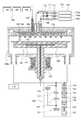
여기에서, 본 실시형태의 특징인 퇴적 전구체(43) 및 결정 핵(44)을 제조하는 것이 가능한 플라즈마 CVD 장치에 대해 도 2 내지 도 4를 사용하여 설명한다.Here, a plasma CVD apparatus capable of producing the
도 2는 플라즈마 CVD 장치의 반응실의 일 구성을 나타낸 것이다. 반응실(100b)은 알루미늄 또는 스테인레스 등 강성이 있는 소재로 형성되고, 내부를 진공배기할 수 있도록 구성되어 있다. 본 실시형태에서 나타낸 반응실(100b)은, 기계적 강도를 높이기 위해 챔버의 소재를 스테인레스로 하고, 내면에 알루미늄 용사를 실행한 것이다. 또한, 본 실시형태에서 나타낸 플라즈마 CVD 장치는, 메인티넌스를 위해 분해가 가능한 챔버 구성으로 하여, 정기적으로 다시 알루미늄 용사를 실행하는 것이 가능한 구성으로 하면 좋다. 반응실(100b)에는 제1 전극(101)(상부 전극이라고도 부른다)과, 제1 전극(101)과 대향하는 제2 전극(102)(하부 전극이라고도 부른다)이 구비되어 있다.2 shows a configuration of a reaction chamber of a plasma CVD apparatus. The
제1 전극(101)에는 고주파 전력 공급수단(103)이 연결되어 있다. 제2 전극(102)은 접지되고, 기판(40)을 재치할 수 있도록 구성되어 있다. 제1 전극(101)은 절연재(116)에 의해 반응실(100b)과 절연 분리됨으로써, 고주파 전력이 누설하지 않도록 구성되어 있다. 절연재(116)로서, 예를 들면, 세라믹 재료를 사용하는 경우에는, 상부 전극의 씰에 나이프 엣지형 메탈 씰 플랜지를 사용하는 것이 곤란하기 때문에, O링 씰을 사용하면 된다.The
이때, 도 2에서는, 제1 전극(101)과 제2 전극(102)을 갖는 용량결합형(평행 평판형)의 구성을 나타내고 있지만, 이것에 한정되지 않는다. 고주파 전력을 공급해서 반응실(100b)의 내부에 글로우 방전 플라즈마를 발생시킬 수 있는 것이면, 유도결합형 등 다른 구성을 적용해도 된다.2, the capacitive coupling type (parallel plate type) structure having the
제1 전극(101)과 제2 전극(102)은, 그것의 일표면이 대략 평행하게 되도록 설치되어 있다. 제1 전극(101)에는, 가스 공급수단(108)에 접속되는 중공부(144)가 설치되어 있다. 중공부(144)는, 가스 라인(146)을 통해 가스 공급수단(108)의 실리콘 또는 게르마늄을 포함하는 퇴적성 기체가 충전된 실린더(110a)에 접속되어 있다. 이 때문에, 중공부(144)의 가스 공급구로부터는, 실리콘 또는 게르마늄을 포함하는 퇴적성 기체가 반응실(100b)에 공급된다.The
가스 공급수단(108)은, 가스가 충전된 실린더(110), 압력 조정 밸브(111), 스톱 밸브(112), 매스 플로우 콘트롤러(113) 등으로 구성되어 있다. 또한, 가스 공급수단(108)은, 실리콘 또는 게르마늄을 포함하는 퇴적성 기체가 충전된 실린더(110a)와, 수소가 충전된 실린더(110b)와, 희석 가스가 충전된 실린더(110c)를 갖는다. 이때, 여기에서는, 희석 가스가 충전된 실린더(110c)를 설치했지만, 반드시 필요로 하지는 않는다.The gas supply means 108 is composed of a
실린더 110a에 충전된 실리콘 또는 게르마늄을 포함하는 퇴적성 기체로서, 대표적으로는, 실란(SiH4) 가스, 디실란(Si2H6) 가스, 게르만(GeH4) 가스, 디게르만(Ge2H6) 가스 등이 있지만, 다른 퇴적성 기체를 사용할 수도 있다.As deposited sex gas containing a silicon or germanium filled in the
실린더 110c에 충전된 희석 가스로서는, 아르곤, 크세논, 크립톤 등의 희가스가 있다.As the diluting gas filled in the
히터 콘트롤러(115)에 의해 온도제어되는 기판 가열 히터(114)는, 제2 전극(102) 내부에 설치되어 있다. 기판 가열 히터(114)가 제2 전극(102) 내부에 설치되는 경우, 열전도 가열방식이 채용된다. 기판 가열 히터(114)는, 예를 들면, 쉬즈 히터(sheathed heater)로 구성된다.The
고주파 전력 공급수단(103)에는, 고주파 전원(104), 정합기(106), 고주파 컷트 필터(129)가 포함되어 있다. 고주파 전원(104)으로부터 공급되는 고주파 전력은, 제1 전극(101)에 공급된다.The high-frequency
고주파 전원(104)은, 60MHz 이하의 고주파 전력을 공급한다. 또한, 제2 전극(102) 위에 재치되는 기판이 제7세대 이상의 대면적 기판인 경우에는, 고주파 전원(104)으로서, 파장이 대략 10m 이상인 고주파 전력을 공급하는 것이 바람직하다. 대표적으로는, 13.56MHz 이하, 예를 들면, 3MHz 이상 13.56MHz 이하의 고주파 전력을 공급하는 것이 바람직하다. 고주파 전원(104)이, 상기 범위의 고주파 전력을 공급함으로써, 제7세대 이상의 대면적 기판을 제2 전극(102) 위에 재치해서 글로우방전을 행하여도, 표면 정재파의 영향을 받지 않고 균일한 플라즈마를 발생시킬 수 있기 때문에, 기판이 대면적이라도 기판 전체에 균질하고 양질의 막을 형성할 수 있다.The high
또한, 고주파 전원(104)으로서 주파수 13.56MHz를 발진하는 전원을 사용하는 경우, 고주파 컷트 필터(129)로서 10pF∼100pF의 가변 콘덴서를 사용하면 된다.When a power source oscillating at a frequency of 13.56 MHz is used as the high
또한, 고주파 컷트 필터(129)로서, 코일을 더 사용하여, 코일과 가변 콘덴서를 사용하는 병렬 공진회로를 구성해도 된다.Further, as the high-
반응실(100b)에 접속되어 있는 배기수단(109)에는 진공배기하는 기능과, 반응 가스를 흘리는 경우에 반응실(100b) 내부를 소정의 압력에 유지하도록 제어하는 기능이 포함되어 있다. 배기수단(109)의 구성으로서는, 버터플라이 밸브 117, 버터플라이 밸브 118, 스톱 밸브(119∼124), 터보 분자펌프 125, 터보 분자펌프 126, 드라이 펌프(127) 등이 포함된다. 이때, 터보 분자펌프 126은 스톱 밸브 124를 거쳐 드라이 펌프(127)와 연결되어 있다.The exhaust means 109 connected to the
반응실(100b) 내부를 진공배기하는 경우에는, 우선, 대략 흡인용(rough vacuum)의 스톱 밸브 119와 대략 흡인용의 스톱 밸브 121을 열어, 반응실(100b) 내부를 드라이 펌프(127)로 배기한 후, 스톱 밸브 119를 닫고, 버터플라이 밸브 117, 스톱 밸브 120을 열어, 진공배기를 행한다. 더구나, 반응실(100b) 내부를 10-5Pa보다도 낮은 압력의 초고진공까지 배기하는 경우에는, 반응실(100b) 내부를 드라이 펌프에 의해 배기한 후, 버터플라이 밸브 117, 스톱 밸브 120 및 스톱 밸브 121을 닫고, 버터플라이 밸브 118로부터 스톱 밸브 122, 123, 124를 열고, 직렬접속된 터보 분자펌프 125, 터보 분자펌프 126 및 드라이 펌프(127)에 의한 배기를 행해서 진공배기한다. 또한, 진공배기를 행한 후에, 반응실(100b) 내부를 가열처리해서 내벽으로부터의 탈가스 처리를 행하는 것이 바람직하다.When the inside of the
제1 전극(101)과 제2 전극(102)의 간격(갭 간격이라고도 부른다)은 적당하게 변경할 수 있도록 구성되어 있다. 이 갭 간격의 조절은, 반응실(100b) 내부에서 제2 전극(102)의 높이의 조정에 의해 행할 수 있다. 벨로우즈(107)를 사용함으로써, 반응실(100b) 내부를 진공에 유지하면서, 갭 간격의 조절을 행할 수 있다.The gap between the
여기에서, 제1 전극(101)의 형상의 일 형태에 대해, 도 3에 나타낸다. 도 3a는 제1 전극(101)을 제2 전극(102)측에서 본 평면도이며, 도 3b는, 도 3a의 A-B에 있어서의 단면도이다.Here, one form of the shape of the
도 3a 및 도 3b에 나타낸 것과 같이, 제1 전극(101)에는 중공부(144)의 가스 공급구가 규칙적으로, 바람직하게는 동일한 간격으로 배치된다. 가스 공급구의 구경은, 제1 전극(101)의 전체면에 있어서 균일하여도 되고, 달라도 된다. 이때, 도면에 나타낸 가스 공급구의 배치는 일례에 지나지 않고, 개시하는 발명의 일 태양이 이것에 한정해서 해석되는 것은 아니다. 예를 들면, 가스 공급구를 제1 전극(101)의 중앙부에만 형성해도 된다.As shown in Figs. 3A and 3B, the
도 4는, 복수의 반응실을 구비한 멀티·챔버·플라즈마 CVD 장치의 일 형태의 개략도를 나타낸 것이다. 이 장치는, 공통실(130), 로드/언로드실(131), 제1 반응실(100a), 제2 반응실(100b), 제3 반응실(100c), 및 제4 반응실(100d)을 구비하고 있다. 로드/언로드실(131)은, 카세트에 장전되는 기판이 공통실(130)의 반송기구(134)에 의해 각 반응실로 반출입되는 매엽식의 구성이다. 공통실(130)과 각 실의 사이에는 게이트 밸브(133)가 구비되어, 각 반응실에서 행해지는 처리가, 서로 간섭하지 않도록 구성되어 있다.FIG. 4 is a schematic view of one embodiment of a multi-chamber plasma CVD apparatus having a plurality of reaction chambers. The apparatus includes a common chamber 130, a load / unload
각 반응실은, 형성하는 박막의 종류에 따라 구분되어 있다. 물론, 반응실의 수는 이것에 한정되는 것은 아니고, 필요에 따라 임의로 증감시킬 수 있다. 또한, 1의 반응실에서 1의 막을 성막하도록 하여도 되고, 1의 반응실에서 복수의 막을 성막하도록 구성해도 된다.Each reaction chamber is divided according to the kind of the thin film to be formed. Of course, the number of reaction chambers is not limited to this, and can be arbitrarily increased or decreased as necessary. In addition, one film may be formed in one reaction chamber, or a plurality of films may be formed in one reaction chamber.
각 반응실에는, 배기수단(109)이 접속되어 있다. 배기수단은 도 2 및 도 4에 나타낸 진공펌프의 조합에 한정되는 것은 아니고, 개략 10-5Pa 내지 10-1Pa의 진공도까지 배기할 수 있는 것이면 다른 진공펌프를 적용해도 된다.An exhausting means 109 is connected to each reaction chamber. The exhaust means is not limited to the combination of the vacuum pumps shown in Figs. 2 and 4, but other vacuum pumps may be used as long as they can evacuate to a degree of vacuum of about 10-5 Pa to 10-1 Pa.
이때, 로드/언로드실(131)에, 드라이 펌프(136) 이외에 초고진공까지 진공배기가 가능한 크라이오 펌프(cryopump)(135)를 연결해도 된다. 크라이오 펌프(135)를 사용함으로써, 로드/언로드실(131)의 압력을 10-5Pa보다도 낮은 압력의 초고진공으로 할 수 있어, 반응실 중의 기판에 퇴적되는 막의 불순물 농도를 저감할 수 있다. 또한, 크라이오 펌프(135)는, 터보 분자펌프 및 드라이 펌프와 비교해서 배기속도가 빠르기 때문에, 개폐 빈도가 높은 로드/언로드실(131)에 크라이오 펌프(135)를 설치함으로써, 스루풋을 향상시킬 수 있다.At this time, in addition to the
가스 공급수단(108)은, 가스가 충전된 실린더(110), 압력 조정 밸브(111), 스톱 밸브(112), 매스 플로우 콘트롤러(113) 등으로 구성되어 있다. 여기에서는 도시하지 않지만, 가스가 충전된 실린더는, 실리콘 또는 게르마늄을 포함하는 퇴적성 기체가 충전된 실린더, 수소가 충전된 실린더, 희석 가스가 충전된 실린더, 반응성 가스(산화성 가스, 질화성 가스, 할로겐 가스 등)가 충전된 실린더, 일 도전형을 부여하는 불순물 원소를 갖는 가스가 충전된 실린더 등을 갖는다.The gas supply means 108 is composed of a
각 반응실에는 플라즈마를 형성하기 위한 고주파 전력 공급수단이 연결되어 있다. 고주파 전력 공급수단에는, 적어도 고주파 전원(104)과 정합기(106)가 포함된다.High-frequency power supply means for forming a plasma is connected to each reaction chamber. The high-frequency power supply unit includes at least a high-
각 반응실은 형성하는 박막의 종류에 따라 나누어 사용하는 것이 가능하다. 각각의 박막에는 최적의 성막 온도가 있으므로, 반응실을 개별적으로 나누어 놓음으로써 성막 온도를 형성하는 막마다 관리하는 것이 용이해진다. 더구나, 동일한 막종을 반복하여 성막할 수 있으므로, 이전에 형성된 막에 기인하는 잔류 불순물의 영향을 배제할 수 있다.Each reaction chamber can be divided depending on the type of the thin film to be formed. Since each thin film has an optimum film forming temperature, it is easy to manage each film forming the film forming temperature by separately dividing the reaction chambers. In addition, since the same film can be formed repeatedly, the influence of residual impurities due to the film formed before can be excluded.
도 2에 나타낸 플라즈마 CVD 장치의 반응실(100b)에 있어서, 반응실의 압력을 종래의 미결정 반도체막의 성막 압력보다 높은 압력, 대표적으로는 450Pa 이상 13332Pa 이하, 바람직하게는 450Pa 이상 2000Pa 이하, 더욱 바람직하게는 500Pa 이상 1500Pa 이하로 하고, 원료 가스로서 실리콘 또는 게르마늄을 포함하는 퇴적성 기체 및 수소를 반응실에 도입하고, 제1 전극(101)에 고주파 전력을 공급하여, 글로우 방전시키면, 분자의 평균 자유 행정이 짧아져, 플라즈마 중에 있어서 전자가 기체 분자에 충돌할 확률이 높아져, 반응 확률이 증가한다. 이 때문에, 플라즈마 중에서 활성의 라디칼이 생성되기 쉽다. 특히, 플라즈마 밀도가 높은 영역에서는 수명이 짧은 활성의 라디칼이 생성되고, 이것이 기상 중에서 반응해서 핵이 형성된다. 핵이 형성되면 기상 중에서 순차 반응이 진행하여 나노미터 사이즈의 퇴적 전구체의 성장이 촉진된다. 이러한 종래의 미결정 반도체막의 성막 압력보다 높은 압력에서의 방전은, 제1 전극(101) 및 제2 전극(102)의 거리가 짧고, 대표적으로는 1mm 이상 20mm 이하, 바람직하게는 4mm 이상 16mm 이하, 더욱 바람직하게는 5mm 이상 10mm 이하의 경우에 발생시키기 쉽다. 이때, 여기에서는, 제1 전극(101) 및 제2 전극(102)의 거리란, 제1 전극(101) 및 제2 전극(102)의 간격을 말한다.In the
퇴적 전구체의 핵이 발생하면, 활성의 라디칼이 핵에 부착되어 퇴적 전구체가 성장한다. 핵 발생에 필요한 라디칼은 핵 성장으로 소비되므로, 새로운 핵의 생성은 억제된다. 따라서, 반응실의 압력과 함께, 제1 전극(101)에 공급하는 전력의 공급 시간(예를 들면, 펄스파 전력에 있어서의 펄스폭, 펄스 주파수), 가스 유량, 가스의 배기 속도를 제어함으로써, 퇴적 전구체의 사이즈 및 생성량을 제어하는 것이 가능하다.When the nuclei of the deposition precursor occur, the active radical attaches to the nucleus and the deposition precursor grows. The radicals needed for nucleation are consumed by the nucleation, so the production of new nuclei is inhibited. Therefore, by controlling the supply time of the electric power to be supplied to the first electrode 101 (for example, the pulse width and the pulse frequency at the pulsed power), the gas flow rate, and the gas exhaust rate together with the pressure in the reaction chamber , It is possible to control the size and amount of the deposition precursor.
퇴적 전구체의 조성은, 공급하는 가스의 선택에 의해 제어할 수 있다. 가스의 종류에 의해, 플라즈마 중에서 생성되는 라디칼이 다르기 때문이다. 따라서, 퇴적 전구체의 성장의 도중에 퇴적성 기체의 종류를 전환함으로써, 다층 구조의 퇴적 전구체의 생성도 가능하다. 이때, 원료 가스가 실리콘 또는 게르마늄을 포함하는 퇴적성 기체의 경우, 퇴적 전구체는, 실리콘, 게르마늄, 또는 실리콘 게르마늄으로 형성된다.The composition of the deposition precursor can be controlled by selection of the supplied gas. This is because the radicals generated in the plasma are different depending on the type of the gas. Therefore, it is also possible to produce a multi-layered deposition precursor by changing the kind of the deposition gas during the growth of the deposition precursor. At this time, in the case of a deposition gas containing silicon or germanium as the source gas, the deposition precursor is formed of silicon, germanium, or silicon germanium.
플라즈마 중에서 퇴적 전구체는 음으로 대전하기 쉽기 때문에, 쿨롬력에 의해 퇴적 전구체끼리의 응집은 억제되는 성질이 있다. 따라서, 본 실시형태에 의해, 단분산에 가까운 퇴적 전구체를 고밀도로 얻을 수 있다.Since the deposition precursor in the plasma is liable to negatively charge, aggregation of the deposition precursors is suppressed by the Coulomb force. Therefore, according to this embodiment, a deposition precursor close to monodisperse can be obtained with high density.
퇴적 전구체의 구조는, 성장에 기여하는 라디칼의 종류 이외에, 퇴적 전구체의 온도가 중요하다. 퇴적 전구체의 온도는, 그것의 표면(퇴적 전구체의 표면)에 입사하는 이온, 전자의 운동에너지, 표면에 있어서의 화학반응에 의한 에너지의 방출 또는 흡수, 중성 가스 분자의 충돌에 의한 가열 또는 냉각 등의 영향을 받아 결정된다.As for the structure of the deposition precursor, in addition to the kinds of radicals contributing to growth, the temperature of the deposition precursor is important. The temperature of the deposition precursor may be controlled by controlling the temperature of the deposition precursor such as the ion incident on its surface (the surface of the deposition precursor), the kinetic energy of the electron, the release or absorption of energy by the chemical reaction on the surface, .
예를 들면, 실리콘의 퇴적 전구체를 생성하는 경우, 실란(SiH4)을 수소로 희석함으로써 결정 구조로 할 수 있다. 이것은, 미결정 실리콘 막을 퇴적하는 경우에 발생하는 표면반응과 동일한 메커니즘이라고 생각되고, 실란이 해리하여 생성된 라디칼과 수소의 반응이, 결정 구조를 갖는 실리콘의 퇴적 전구체의 생성에 주로 기여하고 있기 때문으로 생각된다.For example, when a deposition precursor of silicon is produced, a crystal structure can be obtained by diluting silane (SiH4 ) with hydrogen. This is considered to be the same mechanism as the surface reaction occurring when the microcrystalline silicon film is deposited, and the reaction between the radical and hydrogen generated by dissociation of the silane contributes mainly to the formation of the deposition precursor of the silicon having the crystal structure I think.
이에 따라, 기상 중에서 형성된 질서성을 갖는 퇴적 전구체를 기판 표면에 퇴적시켜, 결정핵으로 하고, 해당 결정 핵을 기판 상에서의 결정성장의 핵으로서 사용할 수 있다. 또한, 퇴적하는 막 중에 결정성의 퇴적 전구체를 포함시킬 수 있다. 더구나, 결정 핵 위에 미결정 반도체막을 퇴적하면, 질서성을 갖는 결정 핵을 결정성장의 핵으로 하여 하지막과의 계면으로부터 결정성장하기 때문에, 하지막 계면으로부터 결정성이 높은 미결정 반도체막을 형성할 수 있다. 더구나, 반응실의 압력을 종래의 미결정 반도체막의 성막 압력보다 높은 압력, 대표적으로는 450Pa 이상 13332Pa 이하, 바람직하게는 450Pa 이상 2000Pa 이하, 바람직하게는 500Pa 이상 1500Pa 이하로 함으로써, 퇴적 전구체의 생성 속도가 증가하기 때문에, 인접하는 결정 핵(44)이 조밀하게 접한 상태에서 하지막(42) 위에 형성시키는 것이 가능한 동시에, 결정립의 사이에 있어서의 비정질 반도체나 저밀도 영역(공동이라고도 한다)이 저감하기 때문에, 결정성이 높은 미결정 반도체막의 성막 속도를 높일 수 있다.
Thus, a deposition precursor having orderedness formed in the vapor phase is deposited on the surface of the substrate to form a crystal nucleus, and the crystal nucleus can be used as nuclei for crystal growth on the substrate. In addition, a crystalline deposition precursor may be included in the deposited film. In addition, when a microcrystalline semiconductor film is deposited on the crystal nucleus, crystal nuclei having orderability are grown as crystals from the interface with the base film, so that a microcrystalline semiconductor film having a high crystallinity can be formed from the base film interface . Furthermore, by setting the pressure of the reaction chamber higher than the deposition pressure of the conventional microcrystalline semiconductor film, typically 450 Pa or more and 13332 Pa or less, preferably 450 Pa or more and 2000 Pa or less, preferably 500 Pa or more and 1500 Pa or less, The
(실시형태 2)(Embodiment 2)
본 실시형태에서는, 실시형태 1에 나타낸 플라즈마 CVD 장치에 있어서, 제1 전극에 적용가능한 구조에 대해서, 도 5 내지 도 10을 사용하여 설명한다.In the present embodiment, a structure applicable to the first electrode in the plasma CVD apparatus shown in
도 5에 나타낸 플라즈마 CVD 장치의 반응실의 일 구성에 있어서, 제1 전극(101)은, 볼록부(141) 및 오목부(143)가 규칙적으로, 바람직하게는 등간격으로 배치된 요철 전극이다. 즉, 볼록 형상의 구조체로 형성되는 볼록부(141)가 규칙적으로, 바람직하게는 등간격으로 배치되어 있다. 또한, 제1 전극(101)의 오목부(143)에는, 가스 공급수단(108)에 접속되는 중공부(144)가 설치되어 있다. 즉, 가스 공급구가 설치되는 공통 평면이 오목부(143)이다. 이때, 여기에서는, 제2 전극(102)의 표면과의 거리가 가까운 가스 공급구를 갖는 영역을 볼록부(141)로 하고, 제2 전극(102)의 표면과의 거리가 먼 가스 공급구를 갖는 영역을 오목부(143)로서 나타낸다.In one configuration of the reaction chamber of the plasma CVD apparatus shown in Fig. 5, the
또한, 중공부(144)는, 가스 라인(146)을 통해 가스 공급수단(108)의 실리콘 또는 게르마늄을 포함하는 퇴적성 기체가 충전된 실린더(110a)에 접속되어 있다. 이 때문에, 오목부(143)에 설치되는 중공부(144)의 가스 공급구로부터는, 실리콘 또는 게르마늄을 포함하는 퇴적성 기체가 반응실(100b)에 공급된다.The
여기에서, 제1 전극(101)의 형상의 일 형태에 대해, 도 6 및 도 7을 사용하여 설명한다. 도 6a 및 도 7a는, 제1 전극(101)을 제2 전극(102)측으로부터 본 평면도이며, 도 6b 및 도 7b는, 도 6a 및 도 7a의 A-B에 있어서의 단면도다. 이때, 도 6a 및 도 7a에 있어서, 요철의 모양을 이해하기 쉽게 하기 위해, 움푹 들어가 있는 영역(즉, 오목부)을 간격이 좁은 해치 패턴으로 나타낸다.Here, one form of the shape of the
도 6a 및 도 6b에 나타낸 것과 같이, 오목부(143)가 형성되는 중공부(144)의 가스 공급구가, 규칙적으로, 바람직하게는 등간격으로 배치된다. 또한, 오목부(143)에는 중공부(144)의 가스 공급구가 설치되어 있다. 복수의 볼록부(141)의 각각은 분리되어 있고, 오목부(143)는 연결된 1개의 평면(공통 평면)이다. 즉, 가스 공급구가 설치되는 공통 평면으로부터 돌출하도록 설치된 볼록 형상의 구조체를 갖고, 상기 볼록 형상의 구조체는 각각 고립되어 있다. 여기에서는, 볼록부(141)를 4각뿔대로 하고 있다. 이때, 볼록부(141)는 이것에 한정되지 않고, 적절히, 3각뿔대, 5각뿔대, 6각뿔대 그 이외의 다각뿔대로 해도 된다. 또한, 볼록부(141)의 모퉁이 및 모서리에 둥근 모따기를 실시하고, 모서리가 둥근 다각뿔대로 하는 것이 바람직하다. 볼록부(141) 및 오목부(143)의 모퉁이 및 모서리에 둥근 모따기를 실시함으로써, 과잉의 전계집중을 저감하는 것이 가능하다. 이 때문에, 국소적인 아크방전을 저감하는 것이 가능해서, 파티클의 발생을 저감할 수 있다.As shown in Figs. 6A and 6B, the gas supply ports of the
또한, 도 7a 및 도 7b에 나타낸 것과 같이, 볼록부(141)가 원뿔대로 되어 있어도 된다. 이때, 오목부(143)에는 중공부(144)의 가스 공급구가 설치되어 있다. 또한, 볼록부(141)의 모퉁이에 둥근 모따기를 실시하여, 모서리가 둥근 원뿔대로 하는 것이 바람직하다. 볼록부(141) 및 오목부(143)의 모퉁이에 둥근 모따기를 시시함으로써, 과잉의 전계집중을 저감하는 것이 가능하다. 이 때문에, 국소적인 아크방전을 저감하는 것이 가능해서, 파티클의 발생을 저감할 수 있다.In addition, as shown in Figs. 7A and 7B, the
또한, 도 6 및 도 7에 나타낸 볼록부(141)에 있어서는, 모서리가 둥근 다각뿔대 또는 원뿔대를 나타냈지만, 도 8a에 나타낸 것과 같이, 다각뿔대 또는 원뿔대의 모퉁이 및 모서리에 둥글게 되지 않도록 모따기를 실시할 수 있다. 대표적으로는, 볼록부(141)를 테이퍼 형상으로 하여 모서리 147을 모따기할 수 있다. 또한, 오목부(143)를 테이퍼 형상으로 하여 모서리 149를 모따기할 수 있다. 볼록부(141) 및 오목부(143)에 있어서, 모서리 147, 149를 모따기함으로써, 해당 영역의 전계집중을 저감하는 것이 가능하여, 파티클의 발생을 저감할 수 있다.6 and 7, a polygonal prism or a truncated cone having rounded corners is shown. However, as shown in Fig. 8A, a chamfer is provided so as not to be rounded at the corners and corners of the truncated pyramid or truncated cone. can do. Typically, the
또한, 도 6 및 도 7에 나타낸 오목부(143)에 있어서, 도 8b에 나타낸 것과 같이, 중공부(144)의 가스 공급구 주변의 모퉁이 및 모서리(155)를 둥글게 해도 된다. 더구나, 도시하지 않지만, 중공부(144)의 가스 공급구 주변에 둥글게 되지 않도록 모따기를 실시해도 된다. 이 결과, 가스 공급구 부근에 있어서의 전계집중을 저감하는 것이 가능하여, 파티클의 발생을 저감할 수 있다.In the
여기에서, 제1 전극(101)의 단면 형상과 전계의 강도에 대해, 도 10을 사용하여 설명한다. 도 10a 및 도 10b는 각각, 계산에 사용한 제1 전극(101)의 단면 형상을 나타내고, 도 10c 및 도 10d는 각각, 전계 시뮬레이터에 의해 계산한 전계의 강도를 나타낸다.Here, the cross-sectional shape of the
도 10a는 제1 전극(101)의 볼록부의 측면이 오목부의 표면과 수직한 형상(제1 형상)을 나타내고, 도 10b는 제1 전극(101)의 볼록부의 단면 형상이 테이퍼 형상(제2 형상)을 나타낸다. 즉, 제1 전극(101)의 볼록부의 측면과 오목부의 표면이 볼록부 내에서 이루는 각도를 θ로 하고, 볼록부의 정수리부의 표면과 측면이 이루는 각도를 γ로 하면, θ이 90°미만이며, γ이 90°보다 큰 형상이다. 이때, 볼록부의 단면 형상이 테이퍼 형상인 경우(도 10b의 경우)에는, 정수리부를 향함에 따라 단면적이 단조하게 작아진다.10A shows a shape in which the side surface of the convex portion of the
도 10a에 있어서는, 오목부의 깊이 d1을 40mm, 인접하는 볼록부의 간격 d2를 20mm, 제1 전극(101) 및 제2 전극(102)의 간격 d3을 20mm로 했다.10A, the depth d1 of the concave portion is 40 mm, the interval d2 of the adjacent convex portions is 20 mm, and the interval d3 of the
도 10b에 있어서는, 오목부의 깊이 d4를 40mm, 인접하는 볼록부에 있어서 제2 전극(102)측의 정수리부의 간격 d5를 60mm, 제1 전극(101) 및 제2 전극(102)의 간격 d6을 20mm로 했다. 이때, 오목부에 있어서 가스 공급구가 형성되는 평면의 직경 d7을 20mm로 했다. 또한, 볼록부의 모퉁이 및 모서리의 곡률반경 R을 10mm로 했다.10B, the depth d4 of the concave portion is 40 mm, the distance d5 of the top portion of the convex portion on the side of the
또한, 도 10 a 및 도 10b의 각각에 있어서, 가스 공급구 근방을 A, 오목부의 중앙 근방을 B, 오목부의 제2 전극(102) 근방을 C, 제1 전극(101)의 볼록부의 튀어나온 부분 근방을 D로 하여, 이들의 전계의 강도에 대해 계산한 결과를 표 1에 나타낸다. 이때, 표 1은, 도 10a에 나타낸 제1 전극(101)의 볼록부의 근방 D의 전계강도를 1로 하고, 그 밖의 영역의 전계강도를 규격화한 것이다. 이때, 제1 전극(101)에 공급한 전력의 주파수는 13.56MHz이다.In each of Figs. 10A and 10B, the vicinity of the gas supply port is denoted by A, the center vicinity of the concave portion is denoted by B, the vicinity of the
도 10c는, 도 10a에 대해서 계산한 전계강도의 분포를 나타내고, 도 10d는, 도 10b에 대해서 계산한 전계강도의 분포를 나타낸 것이다.Fig. 10C shows the distribution of electric field strengths calculated with respect to Fig. 10A, and Fig. 10D shows the distribution of electric field strengths calculated with respect to Fig. 10B.
도 10c에 있어서, 인접하는 볼록부의 사이의 오목부 표면의 근방(A의 근방)에는 전계가 극단적으로 약한 영역(181)이 형성되고, 볼록부와 플라즈마(187) 사이(제1 전극(101)의 볼록부의 근방(D의 근방))에는 전계가 강한 영역(185)이 형성된다.A
한편, 도 10d에 있어서, 테이퍼 각 θ가 작을수록 오목부의 표면까지 전계가 돌아 들어가기 때문에, 오목부에서는 전계가 약한 영역(191)이 형성되고, 볼록부의 정수리부 표면 근방에서는 중 정도의 전계의 영역(193)이 형성된다.On the other hand, in Fig. 10D, since the electric field is moved to the surface of the concave portion as the taper angle? Is smaller, a weak
도 10c와 도 10d를 비교하면, 도 10b의 형상에서는, 볼록부의 정수리부, 특히 볼록부의 모퉁이 및 모서리 근방에 있어서의 전계를 완화할 수 있어, 기판(40) 표면에의 플라즈마 대미지를 저감하는 동시에, 아크방전이 원인인 파티클의 발생을 저감할 수 있다. 또한, 볼록부의 정수리부의 표면의 영역을 작게 할수록, 볼록부의 정수리부 근방에 고밀도 플라즈마 영역을 형성할 수 있다.10C and Fig. 10D, it is possible to alleviate the electric field at the corner of the apex portion of the convex portion, especially at the corners of the convex portion and in the vicinity of the corner, thereby reducing the plasma damage to the surface of the
본 실시형태에 나타낸 제1 전극은, 볼록부(141) 및 오목부(143)를 갖기 때문에, 볼록부(141)의 정수리부에 고밀도 플라즈마 영역을 형성하는 것이 가능하다. 이 때문에, 고밀도 플라즈마 영역에 있어서 반응성이 높아져, 핵 및 퇴적 전구체의 생성을 촉진시킬 수 있다. 이 결과, 실시형태 1과 마찬가지로, 기상 중에서 형성된 질서성을 갖는 퇴적 전구체를 기판 표면에 퇴적시켜 결정 핵으로 하고, 해당 결정 핵을 기판 위에서의 결정성장의 핵으로서 사용할 수 있다. 또한, 퇴적하는 막 중에 결정성의 퇴적 전구체를 포함시킬 수 있다. 더구나, 결정 핵 위에 미결정 반도체막을 퇴적하면, 질서성을 갖는 결정 핵을 결정성장의 핵으로 하여 하지막과의 계면으로부터 결정성장하기 때문에, 하지막 계면으로부터 결정성이 높은 미결정 반도체막을 제조할 수 있다. 더구나, 반응실의 압력을 종래의 미결정 반도체막의 성막 압력보다 높은 압력, 대표적으로는 450Pa 이상 13332Pa 이하, 바람직하게는 450Pa 이상 2000Pa 이하, 바람직하게는 500Pa 이상 1500Pa 이하로 하는 동시에, 볼록부 근방에 있어서 고밀도 플라즈마 영역을 형성함으로써, 퇴적 전구체의 생성 속도가 증가하기 때문에, 인접하는 결정 핵(44)이 조밀하게 접한 상태에서 하지막(42) 위에 형성시키는 것이 가능한 동시에, 결정립의 사이에 있어서의 비정질 반도체나 저밀도 영역(공동이라고도 한다)이 저감하기 때문에, 결정성이 높은 미결정 반도체막의 성막 속도를 높일 수 있다.
Since the first electrode shown in this embodiment has the
(실시형태 3)(Embodiment 3)
본 실시형태에서는, 실시형태 1에 나타낸 플라즈마 CVD 장치에 있어서, 제1 전극에 적용가능한 구조에 대해, 도 9를 사용하여 설명한다. 도 9a는 제1 전극(101)을 제2 전극(102)측에서 본 평면도이며, 도 9b는, 도 9a의 A-B에 있어서의 단면도다. 이때, 도 9a에 있어서, 요철의 모양을 이해하기 쉽게 하기 위해, 움푹 들어가 있는 영역(즉, 오목부)을 간격이 좁은 해치 패턴으로 나타낸다.In this embodiment, a structure applicable to the first electrode in the plasma CVD apparatus shown in
도 9a 및 도 9b에 나타낸 것과 같이, 볼록부(141)에 형성되는 중공부(142)의 가스 공급구가 규칙적으로, 바람직하게는 등간격으로 배치된다. 또한, 도 9b에 나타낸 것과 같이, 볼록부(141)에는 중공부(142)의 가스 공급구가 설치되어 있다. 복수의 볼록부(141)의 각각은 분리되어 있고, 오목부(143)는 연결된 1개의 평면(공통 평면)이다. 여기에서는, 볼록부(141)를 4각뿔대로 하고 있다. 이때, 볼록부(141)는 이것에 한정되지 않고, 적절히, 3각뿔대, 5각뿔대, 6각뿔대 기타의 다각 뿔대로 해도 된다. 또한, 볼록부(141)의 모퉁이 및 모서리를 둥글게 하여, 모서리가 둥근 다각뿔대로 하는 것이 바람직하다. 또한, 볼록부(141)가 원뿔대로 되어 있어도 된다. 더구나, 볼록부(141)의 모퉁이를 둥글게 하여, 모서리가 둥근 원뿔대로 하는 것이 바람직하다.As shown in Figs. 9A and 9B, the gas supply ports of the
글로우 방전에 의해, 볼록부(141)의 정수리부에 있어서 고밀도 플라즈마 영역이 형성되기 때문에, 볼록부(141)의 가스 공급구로부터 반응실로 도입된 원료 가스의 반응이 더욱 촉진된다. 이 때문에, 퇴적 전구체(43)의 생성이 진행하여, 하지막 위에 보다 많은 결정 핵(44)을 치밀하게 퇴적할 수 있다.
Since the high density plasma region is formed at the top of the
(실시형태 4)(Fourth Embodiment)
본 실시형태에서는, 실시형태 1에 나타낸 플라즈마 CVD 장치에 있어서, 제1 전극에 적용가능한 구조에 대해서, 도 11 내지 도 15를 참조해서 설명한다.In the present embodiment, a structure applicable to the first electrode in the plasma CVD apparatus shown in
도 11에 나타낸 플라즈마 CVD 장치의 반응실의 일 구성에 있어서, 제1 전극(101)은, 볼록부(141) 및 오목부(143)가 규칙적으로, 바람직하게는 등간격으로 배치된 요철 전극이다. 즉, 볼록 형상의 구조체로 형성되는 볼록부(141)가 규칙적으로, 바람직하게는 등간격으로 배치되어 있다. 또한, 제1전극(101)의 볼록부(141)에는, 가스 공급수단(108)에 접속되는 중공부 142가 설치되어 있고, 제1 전극(101)의 오목부(143)에는, 가스 공급수단(108)에 접속되는 중공부 144가 설치되어 있다. 즉, 가스 공급구가 설치되는 공통 평면이 오목부(143)이다. 이러한 구조로 함으로써, 볼록부(141)와 오목부(143)로부터 반응실(100b)에 공급되는 가스 종류를 다르게 할 수 있다. 이때, 여기에서는, 제2 전극(102)의 표면과의 거리가 가까운 가스 공급구를 갖는 영역을 볼록부(141)이라고 해서 제2 전극(102)의 표면과의 거리가 먼 가스 공급구를 갖는 영역을 오목부(143)로서 나타낸다.In one configuration of the reaction chamber of the plasma CVD apparatus shown in Fig. 11, the
여기에서, 중공부 142와 중공부 144로부터 흘리는 가스의 종류는 필요에 따라 결정하면 된다. 예를 들면, 중공부 142로부터 퇴적성 가스를 흘리고, 중공부 144로부터 수소 가스를 흘려도 된다. 또는, 중공부 142로부터 수소 가스를 흘리고, 중공부 144로부터 퇴적성 가스를 흘려도 된다. 또는, 중공부 142로부터 퇴적성 가스와 수소 가스의 혼합 가스를 흘리고, 중공부 144로부터 퇴적성 가스를 흘려도 된다. 또는, 중공부 142로부터 퇴적성 가스를 흘리고, 중공부 144로부터 퇴적성 가스와 수소 가스의 혼합 가스를 흘려도 된다. 또는, 중공부 142로부터 퇴적성 가스와 수소 가스의 혼합 가스를 흘리고, 중공부 144로부터 수소 가스를 흘려도 된다. 가장 바람직하게는, 중공부 142로부터 수소 가스를 흘리고, 중공부 144로부터 퇴적성 가스와 수소 가스의 혼합 가스를 흘리는 것이다. 중공부 142로부터 수소 가스를 흘리고, 중공부 144로부터 퇴적성 가스와 수소 가스의 혼합 가스를 흘림으로써, 형성되는 미결정 반도체막의 결정성을 향상시킬 수 있다.Here, the kinds of gas to be discharged from the
이때, 성막 도중에 가스의 유량비를 바꾸어도 된다. 예를 들면, 성막 초기에는 퇴적성 가스의 유량비를 높게 하고, 성막 후기에는 희석율을 높게 함으로써, 결정성을 향상시킬 수 있다.At this time, the flow rate ratio of the gas may be changed during the film formation. For example, crystallinity can be improved by increasing the flow rate ratio of the deposition gas at the initial stage of deposition and increasing the dilution rate at the latter stage of deposition.
또한, 제1 전극(101)은, 복수의 확산판을 가져도 된다(도 12를 참조). 도 12에서는, 가스 라인 145로부터 공급된 가스는, 확산판 151에서 확산한 후, 확산판 151의 관통공 153을 통과하여, 볼록부(141)에 설치되는 중공부 142의 도입구로부터, 반응실(100b)에 공급된다. 또한, 가스 라인 146으로부터 공급된 가스는, 확산판 152에서 확산한 후, 확산판 152의 관통공 154를 통과하여, 오목부(143)에 설치된 중공부 144의 도입구로부터, 반응실(100b)에 공급된다. 도 12에 나타낸 것과 같이, 제1 전극(101)은 확산판 151 및 확산판 152를 갖는 것에 의해, 가스 라인 145 및 가스 라인 146으로부터 도입된 가스가 제1 전극(101) 내부에서 충분하게 확산되어, 균질한 가스를 반응실(100b)에 공급할 수 있으므로, 기판 위에 균질하고 양질의 막을 형성할 수 있다.In addition, the
여기에서, 제1 전극(101)의 형상의 일 형태에 대해서, 도 13 및 도 14를 참조해서 설명한다. 도 13a 및 도 14a는, 제1 전극(101)을 제2 전극(102)측에서 본 평면도이며, 도 13b 및 도 14b는, 도 13a 및 도 14a의 A-B에 있어서의 단면도다. 이때, 도 13a 및 도 14a에 있어서, 요철의 모양을 이해하기 쉽게 하기 위해, 움푹 들어가 있는 영역(즉, 오목부)을 간격이 좁은 해치 패턴으로 나타낸다.Here, one form of the shape of the
도 13a 및 도 13b에 나타낸 것과 같이, 볼록부(141)에 형성되는 중공부 142의 가스 공급구과, 오목부(143)에 형성되는 중공부 144의 가스 공급구가 규칙적으로, 바람직하게는 등간격으로 배치된다. 또한, 볼록부(141)에는 중공부 142의 가스 공급구가 설치되어 있고, 오목부(143)에는 중공부 144의 가스 공급구가 설치되어 있다. 복수의 볼록부(141)의 각각은 분리되어 있고, 오목부(143)는 연결된 1개의 평면(공통 평면)이다. 즉, 가스 공급구가 설치되는 공통 평면으로부터 돌출하도록 설치된 볼록 형상의 구조체를 갖고, 상기 볼록 형상의 구조체는 각각 고립되어 있다. 여기에서는, 볼록부(141)를 4각뿔대로 하고 있다. 이때, 볼록부(141)는 이것에 한정되지 않고, 적절히, 3각뿔대, 5각뿔대, 6각뿔대 기타의 다각뿔대로 해도 된다. 또한, 볼록부(141)의 모퉁이 및 모서리에 둥근 모따기를 실시하여, 모서리가 둥근 다각뿔대로 하는 것이 바람직하다. 볼록부(141) 및 오목부(143)의 모퉁이 및 모서리에 둥근 모따기를 실시함으로써, 과잉의 전계집중을 저감하는 것이 가능하다. 이 때문에, 국소적인 아크방전을 저감하는 것이 가능해서, 파티클의 발생을 저감할 수 있다.13A and 13B, the gas supply port of the
또한, 도 14a 및 도 14b에 나타낸 것과 같이, 볼록부(141)가 원뿔대로 되어 있어도 된다. 또한, 볼록부(141)에는 중공부 142의 가스 공급구가 설치되어 있고, 오목부(143)에는 중공부 144의 가스 공급구가 설치되어 있다. 이때, 볼록부(141)의 모퉁이에 둥근 모따기를 실시하여, 모서리가 둥근 원뿔대로 하는 것이 바람직하다. 대표적으로는, 볼록부(141)를 테이퍼 형상으로 하고, 모서리 156, 158을 모따기할 수 있다. 또한, 오목부(143)를 테이퍼 형상으로 할 수 있다. 볼록부(141) 및 오목부(143)를 테이퍼 형상으로 하고, 모서리 156, 158을 모따기함으로써, 해당 영역의 전계집중을 저감하는 것이 가능해서, 파티클의 발생을 저감할 수 있다(도 15a를 참조). 볼록부(141)를 원뿔대로 하고, 볼록부(141) 및 오목부(143)의 모퉁이에 둥근 모따기를 실시함으로써, 과잉의 전계집중을 저감하는 것이 가능하다. 이 때문에, 국소적인 아크방전을 저감하는 것이 가능해서, 파티클의 발생을 저감할 수 있다Further, as shown in Figs. 14A and 14B, the
또한, 도 13 및 도 14에 나타낸 볼록부(141)에 있어서는, 모서리가 둥근 다각뿔대 또는 원뿔대를 나타냈지만, 다각뿔대 또는 원뿔대의 모퉁이 및 모서리에 둥글게 되지 않도록 모따기를 실시해도 된다.In the
또한, 중공부 144의 가스 공급구 주변의 모퉁이 및 모서리(157)를 둥글게 해도 된다(도 15b를 참조). 더구나, 도시하지 않지만, 중공부 144의 가스 공급구 주변에 둥글게 되지 않도록 모따기를 실시해도 된다. 이 결과, 가스 공급구 부근에 있어서의 전계집중을 저감하는 것이 가능해서, 파티클의 발생을 저감할 수 있다.Further, corners and
이때, 실리콘의 퇴적 전구체를 생성하는 경우, 실란(SiH4)을 수소로 희석함으로써 결정 구조로 할 수 있다. 이것은, 미결정 실리콘 막을 퇴적하는 경우에 발생하는 표면반응과 동일한 메커니즘이라고 생각되고, 실란이 해리해서 생성된 라디칼과 수소의 반응이, 결정 구조를 갖는 실리콘의 퇴적 전구체의 생성에 주로 기여하고 있기 때문으로 생각된다.At this time, when a deposition precursor of silicon is produced, a crystalline structure can be obtained by diluting silane (SiH4 ) with hydrogen. This is considered to be the same mechanism as the surface reaction that occurs when the microcrystalline silicon film is deposited, and the reaction between the radical and hydrogen generated by the dissociation of the silane contributes mainly to the formation of the deposition precursor of the silicon having the crystal structure I think.
이 경우, 예를 들면, 오목부에 설치된 중공부 144의 가스 공급구로부터 공급하는 가스를 실란 가스 또는 수소 희석의 실란 가스로 하면, 퇴적 전구체의 성장이 촉진되어, 기판(40)에 퇴적하는 막의 퇴적 속도를 향상시킬 수 있다. 한편, 오목부에 설치된 중공부 144의 가스 공급구로부터 공급하는 가스를 크세논, 크립톤, 아르곤 등의 희가스로 하면, 희가스의 여기종에 의해 실란의 분해가 촉진되어 고차 라디칼의 생성에 기여하게 된다.In this case, for example, when the gas to be supplied from the gas supply port of the
본 실시형태에 나타낸 제1 전극은, 볼록부(141) 및 오목부(143)를 갖기 때문에, 볼록부(141)의 정수리부에 고밀도 플라즈마 영역을 형성하는 것이 가능하다. 이 때문에, 고밀도 플라즈마 영역에 있어서 반응성이 높아져, 핵 및 퇴적 전구체의 생성을 촉진시킬 수 있다. 이 결과, 실시형태 1과 마찬가지로, 기상 중에서 형성된 질서성을 갖는 퇴적 전구체를 기판 표면에 퇴적시켜 결정 핵으로 하고, 해당 결정 핵을 기판 상에서의 결정성장의 핵으로서 사용할 수 있다. 또한, 퇴적하는 막 중에 결정성의 퇴적 전구체를 포함시킬 수 있다. 더구나, 결정 핵 위에 퇴적하면, 질서성을 갖는 결정 핵을 결정성장의 핵으로 하여 하지막과의 계면으로부터 결정성장하기 때문에, 하지막 계면으로부터 결정성이 높은 미결정 반도체막을 형성할 수 있다. 더구나, 반응실의 압력을 종래의 미결정 반도체막의 성막 압력보다 높은 압력, 대표적으로는 450Pa 이상 13332Pa 이하, 바람직하게는 450Pa 이상 2000Pa 이하, 바람직하게는 500Pa 이상 1500Pa 이하로 한다 동시에, 볼록부 근방에 있어서 고밀도 플라즈마 영역을 형성함으로써, 퇴적 전구체의 생성 속도가 증가하기 때문에, 인접하는 결정 핵(44)이 조밀하게 접한 상태에서 하지막(42) 위에 형성시키는 것이 가능한 동시에, 결정립의 사이에 있어서의 비정질 반도체나 저밀도 영역(공동이라고도 한다)이 저감하기 때문에, 결정성이 높은 미결정 반도체막의 성막 속도를 높일 수 있다.
Since the first electrode shown in this embodiment has the
(실시형태 5)(Embodiment 5)
본 실시형태에서는, 실시형태 1 내지 실시형태 4보다 더욱 결정성이 높은 미결정 반도체막의 형성방법에 대해 설명한다.In this embodiment mode, a method of forming a microcrystalline semiconductor film having higher crystallinity than
본 실시형태에서는, 도 1의 퇴적 전구체(43) 및 미결정 반도체막(46)의 원료 가스로서, 실리콘 또는 게르마늄을 포함하는 퇴적성 기체 및 수소 이외에, 아르곤, 크세논, 크립톤 등의 희가스를 사용하는 것을 특징으로 한다.In this embodiment, rare gas such as argon, xenon, or krypton is used as a source gas for the
원료 가스로서, 아르곤, 크세논, 크립톤과 같은 여기 에너지가 작고, 또한, 실란 및 수소의 해리 에너지에 가까운 준안정 에너지를 갖는 희가스를 사용함으로써, 플라즈마 중에 있어서의 전자밀도 및 수소 라디칼 양이 증가한다. 또한, 전자 온도가 저하하기 때문에, 플라즈마 전위차가 감소하고, 미결정 반도체막에의 대미지가 저감하여, 결정성이 높은 미결정 반도체막(46)을 형성할 수 있다. 또한, 희가스를 원료 가스에 사용함으로써, 플라즈마가 안정되고, 실리콘 또는 게르마늄을 포함하는 퇴적성 기체, 및 수소의 해리가 촉진되어, 활성의 라디칼의 양이 증가한다. 이 때문에, 활성의 라디칼끼리의 반응이 촉진되어, 퇴적 전구체(43)의 생성 속도 및 미결정 반도체막(46)의 성막 속도가 높아진다. 또한, 성막 속도가 높아지면, 미결정 반도체막(46)의 퇴적시간이 짧아져, 퇴적중에 받아들이는 반응실 내의 불순물 양이 저감하기 때문에, 미결정 반도체막(46)에 포함되는 불순물 양이 저감하여, 미결정 반도체막(46)의 결정성을 높일 수 있다.
By using a rare gas having a small excitation energy such as argon, xenon and krypton as the source gas and having metastable energy close to the dissociation energy of silane and hydrogen, the electron density and hydrogen radical content in the plasma are increased. In addition, since the electron temperature is lowered, the plasma potential difference is reduced, the damage to the microcrystalline semiconductor film is reduced, and the
(실시형태 6)(Embodiment 6)
본 실시형태에서는, 광전 변환장치의 일 형태에 대해, 설명한다. 본 실시형태에 나타낸 광전 변환장치에서는, 실시형태 1 내지 실시형태 5에 나타낸 것과 같은 결정성이 높은 미결정 반도체막이 채용되는 반도체막으로서는, 광전변환을 발휘하는 반도체막이나 도전형을 표시하는 반도체막 등이 있지만, 특히, 광전변환을 발휘하는 반도체막에 채용하는 것이 적합하다. 또는, 광전변환을 발휘하는 반도체막이나 도전형을 표시하는 반도체막과, 다른 막과의 계면에, 결정립의 사이의 틈의 수가 극히 적고, 그것의 크기가 극히 작고, 또한, 결정성이 높은 미결정 반도체막을 형성할 수도 있다.In the present embodiment, one form of the photoelectric conversion device will be described. In the photoelectric conversion device according to the present embodiment, as the semiconductor film employing the microcrystalline semiconductor film having high crystallinity as shown in
전술한 것과 같은 구성을 채용함으로써, 광전변환을 발휘하는 반도체막이나 도전형을 표시하는 반도체막에 의해 생기는 저항(직렬저항)을 저감하여, 광전 변환장치의 특성을 향상시킬 수 있다. 또한, 광전변환을 발휘하는 반도체막이나 도전형을 표시하는 반도체막과, 다른 막과의 계면에 있어서의 광학적·전기적인 손실을 억제하여, 광전변환 효율을 향상시킬 수 있다. 이하, 도 16 및 도 17을 사용하여, 광전 변환장치의 제조방법의 일 형태에 대해 설명한다.By adopting the structure as described above, it is possible to reduce the resistance (series resistance) caused by the semiconductor film that exhibits photoelectric conversion or the semiconductor film that displays the conductivity type, and the characteristics of the photoelectric conversion device can be improved. In addition, the photoelectric conversion efficiency can be improved by suppressing optical and electrical loss at the interface between the semiconductor film exhibiting photoelectric conversion and the semiconductor film exhibiting conductivity type and another film. Hereinafter, one mode of the manufacturing method of the photoelectric conversion device will be described with reference to Figs. 16 and 17. Fig.
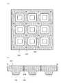
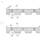
1818
도 16 a에 나타낸 것과 같이, 기판(200) 위에 제1 전극(202)을 형성한다.16 (a), a
기판(200)으로서는, 대표적으로는, 알루미노 실리케이트 유리, 바륨 보로실리케이트 유리, 알루미노 보로실리케이트 유리 등의 전자공업용으로 사용되는 각종 유리 기판이 채용된다. 그 이외에, 석영 기판, 사파이어 기판 등을 사용할 수 있다. 또한, 유기재료를 포함하는 기판을 사용할 수도 있다. 유기재료를 포함하는 기판으로서는, 에폭시 수지, 불포화 폴리에스테르 수지, 폴리이미드 수지, 비스말레이미드 트리아진수지, 시아네이트 수지 등의 열경화성 수지를 포함하는 기판이나, 폴리페닐렌옥시드 수지, 폴리에테르이미드 수지, 불소 수지 등의 열가소성 수지를 포함하는 기판을 사용하면 된다.As the
이때, 기판(200)의 표면은, 텍스처 구조이면 된다. 이에 따라, 광전변환 효율을 향상시키는 것이 가능하다.At this time, the surface of the
또한, 본 실시형태에서는, 빛이 기판(200)의 이면측(도면의 아래쪽)으로부터 입사하는 구성으로 하기 위해, 투광성을 갖는 기판을 채용하지만, 나중에 형성되는 제2 전극측(도면의 윗쪽)으로부터 빛이 입사하는 구성으로 하는 경우에는, 이것에 한정되지 않는다. 이 경우, 실리콘 등의 재료를 포함하는 반도체 기판이나, 금속 재료 등을 포함하는 도전성 기판을 사용해도 된다.In the present embodiment, a light-transmitting substrate is used in order to make the light incident on the back side (lower side of the drawing) of the
제1 전극(202)은, 대표적으로는, 광 투과성을 갖는 도전성 재료를 사용한 전극이 채용된다. 광 투과성을 갖는 도전성 재료에는, In-Sn-Zn-O계, In-Al-Zn-O계, Sn-Ga-Zn-O계, Al-Ga-Zn-O계, Sn-Al-Zn-O계, In-Zn-O계, Sn-Zn-O계, Al-Zn-O계, In-O계, Sn-O계, Zn-O계 등의 산화물(금속 산화물)이 있다. 특히, 산화 인듐, 산화 인듐·주석 합금(ITO), 산화 아연, 산화 인듐·산화 아연 합금 등을 사용하는 것이 바람직하다. 이 이외에, Zn-O-Al-N계의 재료를 사용할 수도 있다. 또한, 무기재료에 한정되지 않고, 유기재료를 사용해도 된다. 유기재료로서는, 폴리아닐린, 폴리피롤, 폴리티오펜, 이들의 유도체 등의 재료(도전성 고분자 재료)를 사용할 수 있다. 제1 전극(202)은, 스퍼터링법, CVD법, 진공증착법, 도포법, 인쇄법 등을 사용해서 형성한다.As the
제1 전극(202)은, 10nm 내지 500nm, 바람직하게는, 50nm 내지 100nm의 두께로 형성한다. 또한, 제1 전극(202)의 시트 저항은, 20Ω/sq. 내지 200Ω/sq. 정도가 되도록 형성한다.The
이때, 본 실시형태에서는, 빛이 기판(200)의 이면측(도면의 아래쪽)으로부터 입사하는 구성으로 하기 위해, 투광성을 갖는 도전성 재료를 사용해서 제1 전극(202)을 형성하고 있지만, 나중에 형성되는 제2 전극측(도면의 윗쪽)으로부터 빛이 입사하는 구성으로 하는 경우에는, 이것에 한정되지 않는다. 이러한 경우에는, 알루미늄, 백금, 금, 은, 구리, 티타늄, 탄탈, 텅스텐 등의 투광성을 갖지 않는 도전성 재료를 사용해서 제1 전극(202)을 형성할 수 있다. 특히, 알루미늄, 은, 티타늄, 탄탈 등의 빛을 반사하기 쉬운 재료를 사용하는 경우에는, 광전변환 효율을 충분히 향상시키는 것이 가능하다.In this embodiment, the
기판(200)의 표면과 마찬가지로, 제1 전극(202)의 표면을, 텍스처 구조로 해도 된다. 또한, 제1 전극(202)에 접하도록, 저저항의 도전성 재료로 이루어진 보조 전극을 별도 형성해도 된다.Like the surface of the
다음에, 도 16b에 나타낸 것과 같이, 제1 전극(202) 위에 제1 도전형을 표시하는 반도체막 204를 형성하고, 제1 도전형을 표시하는 반도체막 204 위에 광전변환을 발휘하는 반도체막 206을 형성하고, 광전변환을 발휘하는 반도체막 206 위에 제2 도전형을 표시하는 반도체막 208을 형성한다.Next, as shown in Fig. 16B, a
제1 도전형을 표시하는 반도체막 204는, 대표적으로는, 도전형을 부여하는 불순물 원소가 첨가된 반도체 재료를 포함하는 반도체막을 사용해서 형성한다. 반도체 재료로서는, 생산성이나 가격 등의 점에서 실리콘을 사용하는 것이 적합하다. 반도체 재료로서 실리콘을 사용하는 경우, 도전형을 부여하는 불순물 원소로서는, n형을 부여하는 인, 비소, p형을 부여하는 붕소, 알루미늄 등이 채용된다.The
이때, 본 실시형태에서는, 빛이 기판(200)의 이면측(도면의 아래쪽)으로부터 입사하는 구성으로 하고 있기 때문에, 제1 도전형을 표시하는 반도체막 204의 도전형(제1 도전형)은 p형으로 하는 것이 바람직하다. 이것은, 홀의 수명이 전자의 수명의 대략 절반으로 짧고, 결과적으로 홀의 확산 길이가 짧은 것, 전자와 홀의 형성이, 광전변환을 발휘하는 반도체막의 빛이 입사하는 쪽에 있어서 많이 행해지는 것 등에 의한 것이다. 이와 같이, 제1 도전형을 p형으로 함으로써, 홀이 소멸하기 전에 전류로서 추출하는 것이 가능하기 때문에, 광전변환 효율의 저하를 억제할 수 있다. 이때, 상기 내용이 문제로 되지 않는 것과 같은 상황, 예를 들면, 광전변환을 발휘하는 반도체막이 충분히 얇은 경우 등에 있어서는, 제1 도전형을 n형으로 해도 된다.In this embodiment, since the light is incident on the back side (lower side in the figure) of the
제1 도전형을 표시하는 반도체막 204의 결정성에 관한 요구는 특별히 없지만, 제1 도전형을 표시하는 반도체막 204에, 실시형태 1 내지 실시형태 5에 나타낸 결정성이 높은 미결정 반도체막을 채용함으로써, 종래의 미결정 반도체막을 채용하는 경우와 비교하여, 직렬저항을 저감하고, 또한, 제1 도전형을 표시하는 반도체막 204와 다른 막과의 계면에 있어서의 광학적·전기적인 손실을 억제 할 수 있으므로, 바람직하다. 물론, 비정질, 다결정, 단결정 등의 다른 결정성의 반도체를 채용하는 것도 가능하다.There is no particular requirement on the crystallinity of the
이때, 제1 도전형을 표시하는 반도체막 204의 표면을, 기판(200)의 표면과 마찬가지로, 텍스처 구조로 해도 된다.At this time, the surface of the
제1 도전형을 표시하는 반도체막 204는, 실리콘을 포함하는 퇴적성 가스, 및 디보란을 사용한 플라즈마 CVD법으로, 형성할 수 있다. 또한, 제1 도전형을 표시하는 반도체막 204는, 1nm 내지 100nm, 바람직하게는, 5nm 내지 50nm의 두께가 되도록 형성한다.The
또한, 도전형을 부여하는 불순물 원소가 첨가되어 있지 않은 실리콘 막을 플라즈마 CVD법 등에 의해 형성한 후, 이온주입 등의 방법으로 붕소를 첨가하여, 제1 도전형을 표시하는 반도체막 204를 형성해도 된다.Further, after forming a silicon film to which an impurity element imparting conductivity type is not added by plasma CVD or the like, boron is added by ion implantation or the like to form a
광전변환을 발휘하는 반도체막 206을 형성한다. 광전변환을 발휘하는 반도체막으로서는, 반도체 재료로서, 실리콘, 실리콘 게르마늄 등을 사용할 수 있다.Thereby forming a
여기에서는, 광전변환을 발휘하는 반도체막 206의 제조방법으로서, 실시형태 1 내지 실시형태 5에 나타낸 미결정 반도체막의 제조공정을 적용한다. 광전변환을 발휘하는 반도체막 206에, 실시형태 1 내지 실시형태 5에 나타낸 미결정 반도체막을 채용함으로써, 종래의 미결정 반도체막을 채용하는 경우와 비교해서 직렬저항을 저감하고, 또한, 반도체막 204와 다른 막과의 계면에 있어서의 광학적·전기적인 손실을 억제할 수 있다.Here, as the manufacturing method of the
이때, 광전변환을 발휘하는 반도체막 206에는 충분한 광흡수가 요구되기 때문에, 그것의 두께는, 100nm 내지 10μm 정도로 하는 것이 바람직하다.At this time, since the
본 실시형태에서는, 제2 도전형을 n형으로 한다. 제2 도전형을 표시하는 반도체막 208은, 도전형을 부여하는 불순물 원소로서 인이 첨가된 실리콘 등의 재료를 사용해서 형성할 수 있다. 제2 도전형을 표시하는 반도체막 208에 사용되는 반도체 재료는, 제1 도전형을 표시하는 반도체막 204와 동일하다.In the present embodiment, the second conductivity type is n-type. The
제2 도전형을 표시하는 반도체막 208은, 제1 도전형을 표시하는 반도체막 204와 마찬가지로 형성할 수 있다. 예를 들면, 실리콘을 포함하는 퇴적성 가스, 및 포스핀을 사용한 플라즈마 CVD법으로, 형성할 수 있다. 제2 도전형을 표시하는 반도체막 208에 대해서도, 실시형태 1 내지 실시형태 5에 나타낸 결정성이 높은 미결정 반도체막을 채용하는 것이 바람직하다.The
이때, 본 실시형태에서는, 빛이 기판(200)의 이면측(도면의 아래 쪽)으로부터 입사하는 구성으로 하고 있기 때문에, 제2 도전형을 표시하는 반도체막 208의 도전형(제2 도전형)을 n형으로 하고 있지만, 개시하는 발명의 일 형태는 이것에 한정되지 않는다. 제1 도전형을 n형으로 하는 경우에는, 제2 도전형이 p형이 된다.In this embodiment, since the light is incident on the back side (lower side of the drawing) of the
상기한 공정에 의해, 제1 도전형을 표시하는 반도체막 204, 광전변환을 발휘하는 반도체막 206, 제2 도전형을 표시하는 반도체막 208을 갖는 유닛 셀(210)이 완성된다.By the above process, the
동일 기판 위에 복수의 유닛 셀을 형성하기 위해, 레이저 가공법에 의해 유닛 셀(210) 및 제1 전극(202)을 관통하는 개구 C0∼Cn을 형성한다. 해당 공정에 의해, 제1 전극(202)이 분할되어, 제1 전극 T1∼Tn으로 된다. 또한, 유닛 셀(210)이 분할되어, 유닛 셀 K1∼Kn이 된다(도 16c 참조).In order to form a plurality of unit cells on the same substrate, openings C0 to Cn passing through the
개구 C0, C2, C4, …Cn-2, Cn은 절연 분리용의 개구이다. 개구 C1, C3, C5, … Cn-1은, 제1 전극(202) 및 나중에 형성되는 제2 전극의 접속을 형성하기 위한 개구이다. 제1 전극(202) 및 유닛 셀(210)이 적층된 상태에서 레이저 가공을 행함으로써, 가공시에 있어서, 기판(200)으로부터의 제1 전극(202)의 박리를 방지할 수 있다.The openings C0 , C2 , C4 , ... Cn-2 , and Cn are openings for insulation isolation. The openings C1 , C3 , C5 , ... Cn-1 is an opening for forming the connection of the
다음에, 개구 C0, C2, C4, …Cn-2, Cn을 충전하면서, 그 개구의 상단부를 덮는 절연 수지층 Zo∼Zn을 형성한다(도 16d 참조). 절연 수지층 Z0∼Zn은 스크린인쇄법에 의해, 아크릴계, 페놀계, 에폭시계, 폴리이미드계 등의 절연성이 있는 수지재료를 사용해서 형성하면 된다. 예를 들면, 페녹시 수지에 시클로헥산, 이소포론, 고저항 카본블랙, 에로실(aerosil), 분산제, 소포제, 레벨링제를 혼합시킨 수지 조성물을 사용하여, 스크린인쇄법에 의해 개구 C0, C2, C4, …Cn-2, Cb을 충전하도록 절연 수지 패턴을 형성한다. 절연 수지 패턴을 형성한 후, 160℃ 오븐 중에서 20분간 열경화시켜, 절연 수지층 Z0∼Zn을 얻는다.Next, the openings C0 , C2 , C4 , ... Cn-2 , and Cn , the insulating resin layers Zo to Zn covering the upper ends of the openings are formed (see FIG. 16D). The insulating resin layers Z0 to Zn may be formed by a screen printing method using an insulating resin material such as an acrylic resin, a phenol resin, an epoxy resin, or a polyimide resin. For example, a resin composition obtained by mixing phenoxy resin with cyclohexane, isophorone, high-resistance carbon black, aerosil, a dispersant, a defoaming agent, and a leveling agent is used to form openings C0 and C2 , C4 , ... Cn-2 , and Cb . Isolated after forming the resin pattern was thermally cured 20 minutes in a 160 ℃ oven, the insulating resin layer to obtain a ~Z0 Zn.
다음에, 제2 전극 E0∼En을 형성한다(도 17 참조). 제2 전극 E0∼En은, 금속 등의 도전성 재료를 사용해서 형성한다. 예를 들면, 알루미늄, 은, 티타늄, 탄탈 등의 빛을 반사하기 쉬운 재료를 사용해서 형성할 수 있다. 빛을 반사하기 쉬운 재료를 사용해서 형성하는 경우, 광전변환을 발휘하는 반도체막에 있어서 완전히 흡수되지 않았던 빛을 재차, 광전변환을 발휘하는 반도체막에 입사시킬 수 있고, 광전변환 효율을 향상시키는 것이 가능하기 때문에, 바람직하다.Next, to form a second electrode E0 ~En (see FIG. 17). A second electrode E0 ~En is formed using a conductive material such as metal. For example, it can be formed using a material which is liable to reflect light such as aluminum, silver, titanium, or tantalum. It is possible to make the light which has not been completely absorbed by the semiconductor film exhibiting photoelectric conversion to be incident again on the semiconductor film exhibiting photoelectric conversion and to improve the photoelectric conversion efficiency It is preferable.
제2 전극 E0∼En의 형성방법으로서는, 스퍼터링법, 진공증착법, CVD법, 도포법, 인쇄법 등이 있다. 또한, 제2 전극 E0∼En은, 10nm 내지 500nm, 바람직하게는, 50nm 내지 100nm의 두께로 형성한다.As the method for forming the second electrode E0 ~En, there is such as a sputtering method, a vacuum vapor deposition method, CVD method, a coating method, a printing method. In addition, the second electrode E0 ~En are to form a 10nm to 500nm, preferably 50nm to 100nm in thickness.
이때, 본 실시형태에서는, 빛이 기판(200)의 이면측(도면의 아래쪽)으로부터 입사하는 구성으로 하기 때문에, 투광성을 갖지 않는 재료를 사용해서 제2 전극 E0∼En을 형성하고 있지만, 제2 전극 E0∼En의 구성은 이것에 한정되지 않는다. 예를 들면, 제2 전극 E0∼En측(도면의 윗쪽)으로부터 빛이 입사하는 구성으로 하는 경우에는, 제2 전극 E0∼En은, 제1 전극(202)에 나타낸 투광성을 갖는 도전성 재료를 사용해서 형성할 수 있다.At this time, in this embodiment, although the light is due to the configuration that is incident from the back surface (bottom in the drawing) of the
각각의 제2 전극 E0∼En은, 개구 C1, C3, C5, …Cn-1에 있어서 제1 전극 T1∼Tn과 접속하도록 형성한다. 즉 개구 C1, C3, C5, …Cn-1에도 제2 전극 E0∼En을 충전한다. 이렇게 하여, 예를 들면, 제2 전극 E1은 제1 전극 T2와 전기적으로 접속하고, 제2 전극 En-1은 제1 전극 Tn과 전기적으로 접속한다. 즉, 제2 전극은, 인접하는 제1 전극과의 전기적인 접속을 얻을 수 있고, 유닛 셀 K1∼Kn은 직렬로 전기적인 접속을 한다.Each of the second electrodes E0 to En has openings C1 , C3 , C5 , ... Cn-1 to the first electrodes T1 to Tn . That is, the openings C1 , C3 , C5 , ... And Cn-1 charge to the second electrodes E0 ~En even. Thus, for example, the second electrode E1 is electrically connected to the first electrode T2, and the second electrode En-1 is electrically connected to the first electrode Tn . That is, the second electrode can obtain an electrical connection with the adjacent first electrode, and the unit cells K1 to Kn are electrically connected in series.
이때, 제2 전극 E0∼En에 접하도록, 저저항의 도전성 재료로 이루어진 보조 전극을 형성해도 된다.At this time, in contact with the second electrode E0 ~En, it may be formed an auxiliary electrode made of a conductive material having a low resistance.
밀봉수지층(212)은, 에폭시 수지, 아크릴 수지, 실리콘 수지를 사용해서 형성한다. 밀봉수지층(212)은, 제2 전극 E0과 제2 전극 En 위에 개구부 214, 개구부 216을 형성한다. 해당 개구부 214, 216에 있어서, 제2 전극 E0과 제2 전극 En은 각각, 외부 배선과 접속한다.The sealing
이상과 같이 해서, 기판(200) 위에 제1 전극 Tn, 유닛 셀 Kn, 및 제2 전극 En으로 이루어진 유닛 셀 Un이 형성된다. 또한, 제1 전극 Tn은 인접하는 제2 전극 En-1과 개구 Cn-1에 있어서 접속한다. 이 결과, n개의 유닛 셀이 직렬로 접속하는 광전 변환장치를 제조할 수 있다. 제2 전극 E0는, 유닛 셀 U1에 있어서의 제1 전극 T1의 추출 전극이 된다.As mentioned above, the first electrode on the substrate (200) Tn, the unit cell Kn, and a are the unit cell Un consisting of two electrodes En is formed. Also, the first electrode Tn is connected to the adjacent second electrode En-1 at the opening Cn-1 . As a result, a photoelectric conversion device in which n unit cells are connected in series can be manufactured. The second electrode E0 becomes an extraction electrode of the first electrode T1 in the unit cell U1 .
상기한 방법으로, 결정성이 높은 미결정 반도체막을, 광전변환을 발휘하는 반도체막, 제1 도전형을 표시하는 반도체막, 제2 도전형을 표시하는 반도체막 중 어느 한개에 사용한 광전 변환장치를 제조할 수 있다. 그리고, 이에 따라, 광전 변환장치의 변환 효율을 높일 수 있다. 이때, 결정성을 높인 미결정 반도체막은, 광전변환을 발휘하는 반도체막, 제1 도전형을 표시하는 반도체막, 제2 도전형을 표시하는 반도체막 중 어느 한개에 이용되고 있으면 되고, 그것의 어느 것에 사용하는지는 적절히 변경이 가능하다. 또한, 상기 반도체막의 복수에 결정립 사이의 틈의 수가 극히 적고, 그 크기가 극히 작고, 또한, 결정성이 높은 미결정 반도체막을 사용하는 경우에는, 보다 효과적이다.With the above-described method, the microcrystalline semiconductor film having a high crystallinity can be obtained by forming a photoelectric conversion device used for either a semiconductor film exhibiting photoelectric conversion, a semiconductor film showing a first conductivity type, or a semiconductor film showing a second conductivity type can do. Thus, the conversion efficiency of the photoelectric conversion device can be increased. At this time, the microcrystalline semiconductor film with an increased crystallinity may be used either in a semiconductor film that exhibits photoelectric conversion, a semiconductor film that displays a first conductivity type, or a semiconductor film that displays a second conductivity type. It is possible to change it appropriately. It is also more effective to use a microcrystalline semiconductor film having extremely small number of gaps between crystal grains in the semiconductor film, extremely small size, and high crystallinity.
이때, 본 실시형태에서는, 1개의 유닛 셀을 갖는 광전 변환장치를 나타냈지만, 적절히 2개 이상의 유닛 셀을 적층한 광전 변환장치로 할 수 있다.In this embodiment, a photoelectric conversion device having one unit cell is shown, but a photoelectric conversion device in which two or more unit cells are appropriately stacked can be used.
본 실시형태는, 다른 실시형태와 적절히 조합해서 사용할 수 있다.
This embodiment can be used in combination with other embodiments as appropriate.
(실시형태 7)(Seventh Embodiment)
도 18에, 이전의 실시형태에서 나타낸 광전 변환장치(501)를 사용한 태양광 발전 시스템의 예를 나타낸다. 충전 제어회로(500)는, 1 또는 복수의 광전 변환장치(501)로부터 공급되는 전력을 사용하여, 축전지(502)를 충전한다. 또한, 축전지(502)가 충분하게 충전되어 있는 경우에는, 광전 변환장치(501)로부터 공급되는 전력을 부하(504)에 직접 출력한다.18 shows an example of a photovoltaic power generation system using the
축전지(502)로서 전기 이중층 커패시터를 사용하면, 충전에 화학반응을 필요로 하지 않기 때문에, 급속한 충전이 가능하다. 또한, 화학반응을 이용하는 납 축전지 등과 비교하여, 수명을 8배 정도, 충방전 효율을 1.5배 정도로 높일 수 있다. 본 실시형태에서 나타낸 태양광 발전 시스템은, 조명, 전자기기 등, 전력을 사용하는 다양한 부하(504)에 대해 사용할 수 있다.The use of an electric double layer capacitor as the
이때, 본 실시형태는, 다른 실시형태와 적절히 조합해서 사용할 수 있다.At this time, the present embodiment can be used in combination with other embodiments as appropriate.
[실시예 1][Example 1]
본 실시예에서는, 고압 조건, 또는, 아르곤 첨가 조건에 의해, 미결정 반도체막의 결정성이 향상되는 모양에 대해, 컴퓨터 시뮬레이션을 사용해서 확인한 결과를 나타낸다. 구체적으로는, 다른 압력, 다른 가스 종류에 있어서의 수소 라디칼의 밀도를 계산하고, 비교한 결과를 나타낸다. 이때, 계산에는, CFD Research Corporation사제의 멀티 피직스 해석 소프트웨어 CFD-ACE+을 사용했다.The present embodiment shows a result of checking the shape of the microcrystalline semiconductor film with improved crystallinity under high pressure or argon addition conditions using computer simulation. Specifically, the density of hydrogen radicals at different pressures and different gas types is calculated and the results are shown. At this time, multi-physics analysis software CFD-ACE + manufactured by CFD Research Corporation was used for calculation.
계산에 있어서의 성막 장치의 모델로서는, 평행 평판 용량 결합형의 CVD장치를 상정했다. 막제조장치의 구성의 개략을 도 19에 나타낸다. 상부 전극(1000)(RF 전극으로 불러도 된다)은, 콘덴서(1010)를 거쳐 고주파 전원(1020)에 접속된다. 기판 스테이지로서 기능하는 하부 전극(1002)은 접지되어 있다.As a model of the film forming apparatus in the calculation, a parallel plate capacitive coupling type CVD apparatus was assumed. The outline of the configuration of the membrane production apparatus is shown in Fig. The upper electrode 1000 (which may be referred to as an RF electrode) is connected to a high
계산에 의해 구해진 수소 라디칼 밀도를 도 20에 나타낸다. 도 20에 있어서, 횡축은 상부 전극으로의 거리(m)를 나타내고, 종축은 수소 라디칼의 밀도(m-3)를 나타낸다. 도 20으로부터, 고압 조건(500Pa, H2)의 경우에는, 저압 조건(100Pa, H2)과 비교하여, 수소 라디칼 밀도가 높아지고 있는 것을 알 수 있다. 이것은, 고압 조건에서는, 저압 조건과 비교하여, 수소의 충돌 해리 레이트가 향상되는 것에 기인하는 것이다.The hydrogen radical density obtained by calculation is shown in Fig. 20, the abscissa axis represents the distance (m) to the upper electrode, and the ordinate axis represents the density (m-3 ) of hydrogen radicals. It can be seen from FIG. 20 that the density of the hydrogen radical is higher in the case of the high pressure condition (500 Pa, H2 ) than in the low pressure condition (100 Pa, H2 ). This is because, under a high-pressure condition, the collision-dissociation rate of hydrogen is improved as compared with a low-pressure condition.
또한, 수소만인 경우(100Pa, H2)와 비교하여, 아르곤을 첨가한 혼합 가스(100Pa, H2+Ar)에서는, 수소 라디칼 밀도가 높아지고 있는 것을 알 수 있다. 아르곤을 첨가함으로써 수소 분자밀도는 저하하기 때문에, 수소의 충돌 해리 레이트는 저하하지만, 기상 중에 있어서의 이하의 반응에 의해, 수소의 해리가 촉진되어, 수소 라디칼 밀도가 높아지고 있는 것으로 고찰된다.It can also be seen that the hydrogen radical density is increased in the mixed gas (100 Pa, H2 + Ar) in which argon is added, as compared with the case of only hydrogen (100 Pa, H2 ). The addition of argon lowers the hydrogen molecule density, so that the collision dissociation rate of hydrogen is lowered. However, it is considered that hydrogen dissociation is promoted by the following reaction in the gas phase, and hydrogen radical density is increased.
Ar+ + H2 → H+ + H + Ar(1)Ar + + H 2 → H + + H + Ar (1)
ArH+ + H2 → H3+ + Ar(2)ArH+ + H2- > H3+ + Ar (2)
H- + ArH+ → Ar + 2H(3)H- + ArH+- > Ar + 2H (3)
e + ArH+→ Ar + H(4)e + ArH+ - > Ar + H (4)
H- + Ar+ → Ar + H(5)H- + Ar+- > Ar + H (5)
Ar(4s) + H2 → 2H + Ar(6)Ar (4s) + H 2 → 2H + Ar (6)
Ar(4p) + H2 → 2H + Ar(7)Ar (4p) + H 2 → 2H + Ar (7)
수소 라디칼 밀도가 높아지는 것에 의해, 수소 라디칼-수소 라디칼의 반응이 촉진된다. 그리고, 해당 반응에 의한 잉여 에너지가 방출되어, 반응 표면에서는 가열의 효과가 생긴다. 예를 들면, 해당 반응이 고차 라디칼(SiHn)x(n=1, 2, 3)의 표면에서 생긴 경우, 잉여 에너지에 의해, 고차 라디칼의 결정성이 향상하게 된다.By increasing the hydrogen radical density, the reaction of the hydrogen radical-hydrogen radical is promoted. Then, surplus energy due to the reaction is released, and a heating effect is produced on the reaction surface. For example, when the reaction occurs on the surface of a higher-order radical (SiHn )x (n = 1, 2, 3), the crystallinity of the higher-order radical is improved by the surplus energy.
이와 같이, 수소 라디칼 밀도는, 양호한 결정성을 구비한 결정 핵의 생성에 큰 영향을 준다. 상기 계산의 결과로부터, 수소 라디칼 밀도를 높임으로써, 미결정 반도체막의 결정성이 향상되는 것이 이해된다.
Thus, the hydrogen radical density has a great influence on the generation of crystal nuclei having good crystallinity. From the results of the calculation, it is understood that the crystallinity of the microcrystalline semiconductor film is improved by increasing the hydrogen radical density.
40 기판 42 하지막 43 퇴적 전구체 44 결정 핵 46 미결정 반도체막 101 전극 102 전극 103 고주파 전력 공급수단 104 고주파전원 106 정합기 107 벨로우즈 108 가스 공급 수단 109 배기수단 110 실린더 111 압력 조정밸브 112 스톱 밸브 113 매스 플로우 콘트롤러 114 기판 가열 히터 115 히터 콘트롤러 116 절연재 117 버터플라이 밸브 118 버터플라이 밸브 119 스톱 밸브 120 스톱 밸브 121 스톱 밸브 124 스톱 밸브 125 터보 분자펌프 126 터보 분자펌프 127 드라이 펌프 129 고주파 컷트 필터 130 공통실 131 로드/언로드 실 133 게이트밸브 134 반송 기구 135 크라이오 펌프 136 드라이 펌프 141 볼록부 142 중공부 143 오목부 144 중공부 145 가스 라인 146 가스 라인 147 모서리 149 모서리 151 확산판 152 확산판 153 관통공 154 관통공 155 모서리 156 모서리 157 모서리 158 모서리 181 영역 185 영역 187 플라즈마 191 영역 193 영역 200 기판 202 전극 204 반도체막 206 반도체막 208 반도체막 210 유닛 셀 212 밀봉수지층 214 개구부 216 개구부 500 충전 제어회로 501 광전 변환장치 502 축전지 504 부하 1000 상부 전극 1002 하부 전극 100a 반응실 100b 반응실 100c 반응실 100d 반응실 1010 콘덴서 1020 고주파 전원 110a 실린더 110b 실린더 110c 실린더40
Claims (16)
Translated fromKorean반응실 내에 상부 전극과 하부 전극이 구비된 플라즈마 CVD 장치를 사용하고,
상기 반응실 내에 반응 가스를 도입하는 단계와,
상기 반응실의 압력을 450Pa 이상 13332Pa 이하로 설정하는 단계와,
상기 상부 전극에 60MHz 이하의 고주파 전력을 공급함으로써 상기 상부 전극과 상기 하부 전극 사이에 플라즈마 영역을 형성하는 단계와,
상기 플라즈마 영역을 포함하는 기상 중에서 결정성을 갖는 퇴적 전구체를 형성하는 단계와,
상기 결정성을 갖는 퇴적 전구체를 퇴적시킴으로써, 5nm 이상 15nm 이하의 결정 핵을 형성하는 단계와,
상기 결정 핵으로부터 결정을 성장시킴으로써, 상기 유닛 셀 내부의 제 1 반도체막, 제 2 반도체막 및 제 3 반도체막 중 어느 한개를 형성하는 단계를 포함하고,
상기 제 1 반도체막의 제 1 도전형과 상기 제 3 반도체막의 제 2 도전형이 서로 다르고,
상기 상부 전극은,
상기 고주파 전력을 공급함으로써 상기 반응실 내에 플라즈마를 형성하는 복수의 볼록부와,
상기 복수의 볼록부의 각각의 정수리부에 설치된 제1 가스 공급구와,
상기 복수의 볼록부 중에서 각각의 2개의 블록부 사이에 설치된 제2 가스 공급구를 갖고,
상기 복수의 볼록부 각각은 테이퍼 형상을 갖고 모따기되어 있으며,
상기 상부 전극과 상기 하부 전극 사이의 간격은 1mm 이상 20mm 이하이고,
상기 제 1 가스 공급구를 통해 상기 반응실에 수소 가스가 도입되고,
상기 제 2 가스 공급구를 통해 상기 반응실에 퇴적성 가스와 수소 가스의 혼합 가스가 도입되는, 광전 변환장치의 제조방법.A method of manufacturing a photoelectric conversion device having a first electrode, a unit cell, and a second electrode on a substrate,
A plasma CVD apparatus having an upper electrode and a lower electrode in a reaction chamber is used,
Introducing a reaction gas into the reaction chamber;
Setting the pressure of the reaction chamber to 450 Pa or more and 13332 Pa or less,
Forming a plasma region between the upper electrode and the lower electrode by supplying a high frequency power of 60 MHz or less to the upper electrode;
Forming a deposition precursor having crystallinity in a vapor phase including the plasma region;
Depositing a deposition precursor having the crystallinity to form crystal nuclei of 5 nm or more and 15 nm or less;
And forming one of the first semiconductor film, the second semiconductor film and the third semiconductor film in the unit cell by growing crystals from the crystal nuclei,
The first conductivity type of the first semiconductor film and the second conductivity type of the third semiconductor film are different from each other,
The upper electrode includes:
A plurality of convex portions for forming a plasma in the reaction chamber by supplying the high frequency electric power,
A first gas supply port provided in each of the apical portions of the plurality of convex portions,
And a second gas supply port provided between each of the two block portions of the plurality of convex portions,
Wherein each of the plurality of convex portions has a tapered shape and is chamfered,
Wherein a distance between the upper electrode and the lower electrode is 1 mm or more and 20 mm or less,
Hydrogen gas is introduced into the reaction chamber through the first gas supply port,
Wherein a mixed gas of a deposition gas and a hydrogen gas is introduced into the reaction chamber through the second gas supply port.
상기 반응 가스와 함께 희가스가 상기 반응실에 도입되는, 광전 변환장치의 제조방법.
14. The method of claim 13,
And a rare gas is introduced into the reaction chamber together with the reaction gas.
상기 반응실 내에 반응 가스를 도입하는 단계와,
상기 반응실의 압력을 450Pa 이상 13332Pa 이하로 설정하는 단계와,
상기 상부 전극에 60MHz 이하의 고주파 전력을 공급함으로써 상기 상부 전극과 상기 하부 전극 사이에 플라즈마 영역을 형성하는 단계와,
상기 플라즈마 영역을 포함하는 기상 중에서 결정성을 갖는 퇴적 전구체를 형성하는 단계와,
상기 결정성을 갖는 퇴적 전구체를 퇴적시킴으로써, 5nm 이상 15nm 이하의 결정 핵을 형성하는 단계를 포함하고,
상기 상부 전극은,
상기 고주파 전력을 공급함으로써 상기 반응실 내에 플라즈마를 형성하는 복수의 볼록부와,
상기 복수의 볼록부의 각각의 정수리부에 설치된 제1 가스 공급구와,
상기 복수의 볼록부 중에서 각각의 2개의 블록부 사이에 설치된 제2 가스 공급구를 갖고,
상기 복수의 볼록부 각각은 테이퍼 형상을 갖고 모따기되어 있으며,
상기 상부 전극과 상기 하부 전극 사이의 간격은 1mm 이상 20mm 이하이고,
상기 제 1 가스 공급구를 통해 상기 반응실에 수소 가스가 도입되고,
상기 제 2 가스 공급구를 통해 상기 반응실에 퇴적성 가스와 수소 가스의 혼합 가스가 도입되는, 미결정 반도체막의 제조방법.A method for producing a microcrystalline semiconductor film by using a plasma CVD apparatus having an upper electrode and a lower electrode in a reaction chamber,
Introducing a reaction gas into the reaction chamber;
Setting the pressure of the reaction chamber to 450 Pa or more and 13332 Pa or less,
Forming a plasma region between the upper electrode and the lower electrode by supplying a high frequency power of 60 MHz or less to the upper electrode;
Forming a deposition precursor having crystallinity in a vapor phase including the plasma region;
And depositing a deposition precursor having the crystallinity to form crystal nuclei of 5 nm or more and 15 nm or less,
The upper electrode includes:
A plurality of convex portions for forming a plasma in the reaction chamber by supplying the high frequency electric power,
A first gas supply port provided in each of the apical portions of the plurality of convex portions,
And a second gas supply port provided between each of the two block portions of the plurality of convex portions,
Wherein each of the plurality of convex portions has a tapered shape and is chamfered,
Wherein a distance between the upper electrode and the lower electrode is 1 mm or more and 20 mm or less,
Hydrogen gas is introduced into the reaction chamber through the first gas supply port,
And a mixed gas of a deposition gas and a hydrogen gas is introduced into the reaction chamber through the second gas supply port.
상기 반응 가스와 함께 희가스가 상기 반응실에 도입되는, 미결정 반도체막의 제조방법.16. The method of claim 15,
And a rare gas is introduced into the reaction chamber together with the reaction gas.
Applications Claiming Priority (6)
| Application Number | Priority Date | Filing Date | Title |
|---|---|---|---|
| JPJP-P-2009-194855 | 2009-08-25 | ||
| JP2009194846 | 2009-08-25 | ||
| JPJP-P-2009-194806 | 2009-08-25 | ||
| JP2009194855 | 2009-08-25 | ||
| JPJP-P-2009-194846 | 2009-08-25 | ||
| JP2009194806 | 2009-08-25 |
Publications (2)
| Publication Number | Publication Date |
|---|---|
| KR20110021652A KR20110021652A (en) | 2011-03-04 |
| KR101722903B1true KR101722903B1 (en) | 2017-04-04 |
Family
ID=43625512
Family Applications (1)
| Application Number | Title | Priority Date | Filing Date |
|---|---|---|---|
| KR1020100077119AExpired - Fee RelatedKR101722903B1 (en) | 2009-08-25 | 2010-08-11 | Method of manufacturing photoelectric conversion device |
Country Status (4)
| Country | Link |
|---|---|
| US (1) | US8207011B2 (en) |
| JP (1) | JP5774826B2 (en) |
| KR (1) | KR101722903B1 (en) |
| TW (1) | TWI524541B (en) |
Families Citing this family (7)
| Publication number | Priority date | Publication date | Assignee | Title |
|---|---|---|---|---|
| US9177761B2 (en)* | 2009-08-25 | 2015-11-03 | Semiconductor Energy Laboratory Co., Ltd. | Plasma CVD apparatus, method for forming microcrystalline semiconductor film and method for manufacturing semiconductor device |
| KR20110021654A (en)* | 2009-08-25 | 2011-03-04 | 가부시키가이샤 한도오따이 에네루기 켄큐쇼 | Manufacturing method of microcrystalline semiconductor film, and manufacturing method of semiconductor device |
| US8513046B2 (en) | 2010-10-07 | 2013-08-20 | Semiconductor Energy Laboratory Co., Ltd. | Photoelectric conversion device and manufacturing method thereof |
| JP5892581B2 (en)* | 2011-08-17 | 2016-03-23 | 国立研究開発法人物質・材料研究機構 | Plasma process equipment |
| TWI733712B (en)* | 2015-12-18 | 2021-07-21 | 美商應用材料股份有限公司 | A diffuser for a deposition chamber and an electrode for a deposition chamber |
| US11266003B2 (en)* | 2017-06-13 | 2022-03-01 | Zaka-Ul-Islam Mujahid | Method and apparatus for generating plasma using a patterned dielectric or electrode |
| JP2019207912A (en)* | 2018-05-28 | 2019-12-05 | 東京エレクトロン株式会社 | Upper electrode assembly, processing apparatus, and manufacturing method of upper electrode assembly |
Citations (3)
| Publication number | Priority date | Publication date | Assignee | Title |
|---|---|---|---|---|
| JP2001093842A (en)* | 1999-09-27 | 2001-04-06 | Kanegafuchi Chem Ind Co Ltd | Plasma cvd apparatus, and method of manufacturing silicon-based thin-film photoelectric converter |
| JP2006237490A (en)* | 2005-02-28 | 2006-09-07 | Sanyo Electric Co Ltd | Plasma processing equipment |
| US20080188062A1 (en)* | 2007-02-02 | 2008-08-07 | Chi-Lin Chen | Method of forming microcrystalline silicon film |
Family Cites Families (21)
| Publication number | Priority date | Publication date | Assignee | Title |
|---|---|---|---|---|
| JPS56122123A (en)* | 1980-03-03 | 1981-09-25 | Shunpei Yamazaki | Semiamorphous semiconductor |
| JPS63166235A (en)* | 1986-12-27 | 1988-07-09 | Nec Corp | Parallel flat plate type plasma cvd system |
| JP4578693B2 (en)* | 2001-02-09 | 2010-11-10 | 株式会社カネカ | Plasma CVD apparatus and silicon-based film manufacturing method using plasma CVD apparatus |
| CN1496584A (en)* | 2001-03-09 | 2004-05-12 | �ձ�������ʽ���� | Vapor phase growth method of metal oxide dielectric film and PZT film |
| JP3837539B2 (en) | 2003-03-25 | 2006-10-25 | 独立行政法人産業技術総合研究所 | Plasma CVD equipment |
| JP4707959B2 (en)* | 2004-02-20 | 2011-06-22 | 日本エー・エス・エム株式会社 | Shower plate, plasma processing apparatus and plasma processing method |
| JP4178202B2 (en) | 2004-03-10 | 2008-11-12 | 三菱重工業株式会社 | Thin film manufacturing method |
| US20050233092A1 (en)* | 2004-04-20 | 2005-10-20 | Applied Materials, Inc. | Method of controlling the uniformity of PECVD-deposited thin films |
| US7785672B2 (en)* | 2004-04-20 | 2010-08-31 | Applied Materials, Inc. | Method of controlling the film properties of PECVD-deposited thin films |
| US7125758B2 (en)* | 2004-04-20 | 2006-10-24 | Applied Materials, Inc. | Controlling the properties and uniformity of a silicon nitride film by controlling the film forming precursors |
| US8083853B2 (en)* | 2004-05-12 | 2011-12-27 | Applied Materials, Inc. | Plasma uniformity control by gas diffuser hole design |
| US8074599B2 (en)* | 2004-05-12 | 2011-12-13 | Applied Materials, Inc. | Plasma uniformity control by gas diffuser curvature |
| US20060005771A1 (en)* | 2004-07-12 | 2006-01-12 | Applied Materials, Inc. | Apparatus and method of shaping profiles of large-area PECVD electrodes |
| US8328939B2 (en)* | 2004-05-12 | 2012-12-11 | Applied Materials, Inc. | Diffuser plate with slit valve compensation |
| JP4451221B2 (en)* | 2004-06-04 | 2010-04-14 | 東京エレクトロン株式会社 | Gas processing apparatus and film forming apparatus |
| DE602006017195D1 (en)* | 2005-04-04 | 2010-11-11 | Dowa Holdings Co Ltd | Process for growing GaN single crystals |
| JP4730034B2 (en)* | 2005-09-20 | 2011-07-20 | 日新電機株式会社 | Method for forming a substrate with silicon dots |
| JP5503857B2 (en)* | 2007-09-14 | 2014-05-28 | 株式会社半導体エネルギー研究所 | Method for manufacturing thin film transistor |
| KR20090095314A (en)* | 2008-03-05 | 2009-09-09 | 삼성전자주식회사 | Crystallization method of amorphous layer and thin film solar cell and fabrication method of the cell adopting the crystallization method |
| US9177761B2 (en)* | 2009-08-25 | 2015-11-03 | Semiconductor Energy Laboratory Co., Ltd. | Plasma CVD apparatus, method for forming microcrystalline semiconductor film and method for manufacturing semiconductor device |
| KR20110021654A (en)* | 2009-08-25 | 2011-03-04 | 가부시키가이샤 한도오따이 에네루기 켄큐쇼 | Manufacturing method of microcrystalline semiconductor film, and manufacturing method of semiconductor device |
- 2010
- 2010-08-11KRKR1020100077119Apatent/KR101722903B1/ennot_activeExpired - Fee Related
- 2010-08-17TWTW099127456Apatent/TWI524541B/ennot_activeIP Right Cessation
- 2010-08-20USUS12/860,283patent/US8207011B2/ennot_activeExpired - Fee Related
- 2010-08-24JPJP2010186932Apatent/JP5774826B2/ennot_activeExpired - Fee Related
Patent Citations (3)
| Publication number | Priority date | Publication date | Assignee | Title |
|---|---|---|---|---|
| JP2001093842A (en)* | 1999-09-27 | 2001-04-06 | Kanegafuchi Chem Ind Co Ltd | Plasma cvd apparatus, and method of manufacturing silicon-based thin-film photoelectric converter |
| JP2006237490A (en)* | 2005-02-28 | 2006-09-07 | Sanyo Electric Co Ltd | Plasma processing equipment |
| US20080188062A1 (en)* | 2007-02-02 | 2008-08-07 | Chi-Lin Chen | Method of forming microcrystalline silicon film |
Also Published As
| Publication number | Publication date |
|---|---|
| JP2011071499A (en) | 2011-04-07 |
| TW201123466A (en) | 2011-07-01 |
| US8207011B2 (en) | 2012-06-26 |
| KR20110021652A (en) | 2011-03-04 |
| TWI524541B (en) | 2016-03-01 |
| US20110053311A1 (en) | 2011-03-03 |
| JP5774826B2 (en) | 2015-09-09 |
Similar Documents
| Publication | Publication Date | Title |
|---|---|---|
| KR101722903B1 (en) | Method of manufacturing photoelectric conversion device | |
| JP2824808B2 (en) | Apparatus for continuously forming large-area functional deposited films by microwave plasma CVD | |
| US5397395A (en) | Method of continuously forming a large area functional deposited film by microwave PCVD and apparatus for the same | |
| JP6103104B2 (en) | Deposition equipment | |
| US20100029038A1 (en) | Manufacturing method of solar cell and manufacturing apparatus of solar cell | |
| KR101203963B1 (en) | Apparatus and method for manufacturing photoelectric conversion elements, and photoelectric conversion element | |
| US20090183771A1 (en) | Plasma processing apparatus, plasma processing method and photoelectric conversion element | |
| US9177761B2 (en) | Plasma CVD apparatus, method for forming microcrystalline semiconductor film and method for manufacturing semiconductor device | |
| US5976257A (en) | Apparatus for continuously forming a large area deposited film by means of microwave plasma CVD process | |
| JPS62271418A (en) | Manufacture of amorphous silicon semiconductor element | |
| KR20110021654A (en) | Manufacturing method of microcrystalline semiconductor film, and manufacturing method of semiconductor device | |
| KR20140006907A (en) | Silicon nitride film deposition method, organic electronic device manufacturing method, and silicon nitride film deposition device | |
| JPH04198482A (en) | Deposited film forming method and deposited film forming apparatus | |
| JP2722114B2 (en) | Method and apparatus for continuously forming large-area functional deposition film by microwave plasma CVD | |
| JP5732558B2 (en) | Photoelectric conversion device and manufacturing method thereof | |
| CN102031503B (en) | Deposition method of silicon thin film | |
| US8772627B2 (en) | Photoelectric conversion device and manufacturing method thereof | |
| JPH10265212A (en) | Method for producing microcrystalline and polycrystalline silicon thin films | |
| CN101480111A (en) | Plasma processing apparatus, plasma processing method, and photoelectric conversion element | |
| JP2017226924A (en) | Plasma cvd device, crystal silicon group solar cell, and plasma cvd method for manufacturing them | |
| JP2018019107A (en) | Plasma cvd system, crystal silicon-based solar battery, and plasma cvd method for manufacturing the same | |
| TWI732223B (en) | Process reactor for plasma-enhanced chemical vapor deposition and a vacuum installation using such reactor | |
| JP2018026594A (en) | Plasma cvd device and plasma cvd method | |
| JP2009038317A (en) | Thin film solar cell film forming method and film forming apparatus | |
| CN117438491A (en) | Silicon heterojunction solar cell preparation equipment |
Legal Events
| Date | Code | Title | Description |
|---|---|---|---|
| PA0109 | Patent application | St.27 status event code:A-0-1-A10-A12-nap-PA0109 | |
| PG1501 | Laying open of application | St.27 status event code:A-1-1-Q10-Q12-nap-PG1501 | |
| P22-X000 | Classification modified | St.27 status event code:A-2-2-P10-P22-nap-X000 | |
| A201 | Request for examination | ||
| PA0201 | Request for examination | St.27 status event code:A-1-2-D10-D11-exm-PA0201 | |
| P22-X000 | Classification modified | St.27 status event code:A-2-2-P10-P22-nap-X000 | |
| D13-X000 | Search requested | St.27 status event code:A-1-2-D10-D13-srh-X000 | |
| D14-X000 | Search report completed | St.27 status event code:A-1-2-D10-D14-srh-X000 | |
| E902 | Notification of reason for refusal | ||
| PE0902 | Notice of grounds for rejection | St.27 status event code:A-1-2-D10-D21-exm-PE0902 | |
| E13-X000 | Pre-grant limitation requested | St.27 status event code:A-2-3-E10-E13-lim-X000 | |
| P11-X000 | Amendment of application requested | St.27 status event code:A-2-2-P10-P11-nap-X000 | |
| P13-X000 | Application amended | St.27 status event code:A-2-2-P10-P13-nap-X000 | |
| E701 | Decision to grant or registration of patent right | ||
| PE0701 | Decision of registration | St.27 status event code:A-1-2-D10-D22-exm-PE0701 | |
| GRNT | Written decision to grant | ||
| PR0701 | Registration of establishment | St.27 status event code:A-2-4-F10-F11-exm-PR0701 | |
| PR1002 | Payment of registration fee | St.27 status event code:A-2-2-U10-U11-oth-PR1002 Fee payment year number:1 | |
| PG1601 | Publication of registration | St.27 status event code:A-4-4-Q10-Q13-nap-PG1601 | |
| FPAY | Annual fee payment | Payment date:20200227 Year of fee payment:4 | |
| PR1001 | Payment of annual fee | St.27 status event code:A-4-4-U10-U11-oth-PR1001 Fee payment year number:4 | |
| P22-X000 | Classification modified | St.27 status event code:A-4-4-P10-P22-nap-X000 | |
| PR1001 | Payment of annual fee | St.27 status event code:A-4-4-U10-U11-oth-PR1001 Fee payment year number:5 | |
| PC1903 | Unpaid annual fee | St.27 status event code:A-4-4-U10-U13-oth-PC1903 Not in force date:20220330 Payment event data comment text:Termination Category : DEFAULT_OF_REGISTRATION_FEE | |
| PC1903 | Unpaid annual fee | St.27 status event code:N-4-6-H10-H13-oth-PC1903 Ip right cessation event data comment text:Termination Category : DEFAULT_OF_REGISTRATION_FEE Not in force date:20220330 | |
| P22-X000 | Classification modified | St.27 status event code:A-4-4-P10-P22-nap-X000 |