KR101716369B1 - Auto inspection apparatus and method of laser processing apparatus - Google Patents
Auto inspection apparatus and method of laser processing apparatusDownload PDFInfo
- Publication number
- KR101716369B1 KR101716369B1KR1020150145432AKR20150145432AKR101716369B1KR 101716369 B1KR101716369 B1KR 101716369B1KR 1020150145432 AKR1020150145432 AKR 1020150145432AKR 20150145432 AKR20150145432 AKR 20150145432AKR 101716369 B1KR101716369 B1KR 101716369B1
- Authority
- KR
- South Korea
- Prior art keywords
- image
- laser beam
- damaged
- laser
- processed
- Prior art date
- Legal status (The legal status is an assumption and is not a legal conclusion. Google has not performed a legal analysis and makes no representation as to the accuracy of the status listed.)
- Active
Links
- 238000000034methodMethods0.000titleclaimsabstractdescription46
- 238000007689inspectionMethods0.000titleclaimsabstractdescription17
- 230000001678irradiating effectEffects0.000claimsabstractdescription10
- 238000003754machiningMethods0.000claimsdescription38
- 239000000463materialSubstances0.000claimsdescription14
- 239000004065semiconductorSubstances0.000claimsdescription14
- 238000005259measurementMethods0.000claimsdescription9
- 238000001514detection methodMethods0.000claimsdescription8
- VYZAMTAEIAYCRO-UHFFFAOYSA-NChromiumChemical compound[Cr]VYZAMTAEIAYCRO-UHFFFAOYSA-N0.000claimsdescription6
- WGLPBDUCMAPZCE-UHFFFAOYSA-NTrioxochromiumChemical compoundO=[Cr](=O)=OWGLPBDUCMAPZCE-UHFFFAOYSA-N0.000claimsdescription6
- 229910052804chromiumInorganic materials0.000claimsdescription6
- 239000011651chromiumSubstances0.000claimsdescription6
- 229910000423chromium oxideInorganic materials0.000claimsdescription6
- OKTJSMMVPCPJKN-UHFFFAOYSA-NCarbonChemical compound[C]OKTJSMMVPCPJKN-UHFFFAOYSA-N0.000claimsdescription5
- 229910052799carbonInorganic materials0.000claimsdescription5
- 239000000284extractSubstances0.000claimsdescription5
- XUIMIQQOPSSXEZ-UHFFFAOYSA-NSiliconChemical compound[Si]XUIMIQQOPSSXEZ-UHFFFAOYSA-N0.000description9
- 229910052710siliconInorganic materials0.000description9
- 239000010703siliconSubstances0.000description9
- 230000003287optical effectEffects0.000description6
- 239000000758substrateSubstances0.000description3
- 238000012986modificationMethods0.000description2
- 230000004048modificationEffects0.000description2
- 230000002411adverseEffects0.000description1
- 230000015572biosynthetic processEffects0.000description1
- 238000005530etchingMethods0.000description1
- 238000004080punchingMethods0.000description1
Images


Classifications
- B—PERFORMING OPERATIONS; TRANSPORTING
- B23—MACHINE TOOLS; METAL-WORKING NOT OTHERWISE PROVIDED FOR
- B23K—SOLDERING OR UNSOLDERING; WELDING; CLADDING OR PLATING BY SOLDERING OR WELDING; CUTTING BY APPLYING HEAT LOCALLY, e.g. FLAME CUTTING; WORKING BY LASER BEAM
- B23K26/00—Working by laser beam, e.g. welding, cutting or boring
- B23K26/02—Positioning or observing the workpiece, e.g. with respect to the point of impact; Aligning, aiming or focusing the laser beam
- B23K26/03—Observing, e.g. monitoring, the workpiece
- B23K26/032—Observing, e.g. monitoring, the workpiece using optical means
- H—ELECTRICITY
- H01—ELECTRIC ELEMENTS
- H01L—SEMICONDUCTOR DEVICES NOT COVERED BY CLASS H10
- H01L22/00—Testing or measuring during manufacture or treatment; Reliability measurements, i.e. testing of parts without further processing to modify the parts as such; Structural arrangements therefor
- H01L22/10—Measuring as part of the manufacturing process
- H01L22/12—Measuring as part of the manufacturing process for structural parameters, e.g. thickness, line width, refractive index, temperature, warp, bond strength, defects, optical inspection, electrical measurement of structural dimensions, metallurgic measurement of diffusions
- B—PERFORMING OPERATIONS; TRANSPORTING
- B23—MACHINE TOOLS; METAL-WORKING NOT OTHERWISE PROVIDED FOR
- B23K—SOLDERING OR UNSOLDERING; WELDING; CLADDING OR PLATING BY SOLDERING OR WELDING; CUTTING BY APPLYING HEAT LOCALLY, e.g. FLAME CUTTING; WORKING BY LASER BEAM
- B23K26/00—Working by laser beam, e.g. welding, cutting or boring
- B23K26/0006—Working by laser beam, e.g. welding, cutting or boring taking account of the properties of the material involved
- B—PERFORMING OPERATIONS; TRANSPORTING
- B23—MACHINE TOOLS; METAL-WORKING NOT OTHERWISE PROVIDED FOR
- B23K—SOLDERING OR UNSOLDERING; WELDING; CLADDING OR PLATING BY SOLDERING OR WELDING; CUTTING BY APPLYING HEAT LOCALLY, e.g. FLAME CUTTING; WORKING BY LASER BEAM
- B23K26/00—Working by laser beam, e.g. welding, cutting or boring
- B23K26/02—Positioning or observing the workpiece, e.g. with respect to the point of impact; Aligning, aiming or focusing the laser beam
- B23K26/06—Shaping the laser beam, e.g. by masks or multi-focusing
- B23K26/062—Shaping the laser beam, e.g. by masks or multi-focusing by direct control of the laser beam
- B23K26/0622—Shaping the laser beam, e.g. by masks or multi-focusing by direct control of the laser beam by shaping pulses
- B23K26/0624—Shaping the laser beam, e.g. by masks or multi-focusing by direct control of the laser beam by shaping pulses using ultrashort pulses, i.e. pulses of 1ns or less
- B—PERFORMING OPERATIONS; TRANSPORTING
- B23—MACHINE TOOLS; METAL-WORKING NOT OTHERWISE PROVIDED FOR
- B23K—SOLDERING OR UNSOLDERING; WELDING; CLADDING OR PLATING BY SOLDERING OR WELDING; CUTTING BY APPLYING HEAT LOCALLY, e.g. FLAME CUTTING; WORKING BY LASER BEAM
- B23K26/00—Working by laser beam, e.g. welding, cutting or boring
- B23K26/02—Positioning or observing the workpiece, e.g. with respect to the point of impact; Aligning, aiming or focusing the laser beam
- B23K26/06—Shaping the laser beam, e.g. by masks or multi-focusing
- B23K26/064—Shaping the laser beam, e.g. by masks or multi-focusing by means of optical elements, e.g. lenses, mirrors or prisms
- B—PERFORMING OPERATIONS; TRANSPORTING
- B23—MACHINE TOOLS; METAL-WORKING NOT OTHERWISE PROVIDED FOR
- B23K—SOLDERING OR UNSOLDERING; WELDING; CLADDING OR PLATING BY SOLDERING OR WELDING; CUTTING BY APPLYING HEAT LOCALLY, e.g. FLAME CUTTING; WORKING BY LASER BEAM
- B23K26/00—Working by laser beam, e.g. welding, cutting or boring
- B23K26/08—Devices involving relative movement between laser beam and workpiece
- B23K26/082—Scanning systems, i.e. devices involving movement of the laser beam relative to the laser head
- B—PERFORMING OPERATIONS; TRANSPORTING
- B23—MACHINE TOOLS; METAL-WORKING NOT OTHERWISE PROVIDED FOR
- B23K—SOLDERING OR UNSOLDERING; WELDING; CLADDING OR PLATING BY SOLDERING OR WELDING; CUTTING BY APPLYING HEAT LOCALLY, e.g. FLAME CUTTING; WORKING BY LASER BEAM
- B23K26/00—Working by laser beam, e.g. welding, cutting or boring
- B23K26/36—Removing material
- B23K26/362—Laser etching
- B—PERFORMING OPERATIONS; TRANSPORTING
- B23—MACHINE TOOLS; METAL-WORKING NOT OTHERWISE PROVIDED FOR
- B23K—SOLDERING OR UNSOLDERING; WELDING; CLADDING OR PLATING BY SOLDERING OR WELDING; CUTTING BY APPLYING HEAT LOCALLY, e.g. FLAME CUTTING; WORKING BY LASER BEAM
- B23K26/00—Working by laser beam, e.g. welding, cutting or boring
- B23K26/36—Removing material
- B23K26/40—Removing material taking account of the properties of the material involved
- B—PERFORMING OPERATIONS; TRANSPORTING
- B23—MACHINE TOOLS; METAL-WORKING NOT OTHERWISE PROVIDED FOR
- B23K—SOLDERING OR UNSOLDERING; WELDING; CLADDING OR PLATING BY SOLDERING OR WELDING; CUTTING BY APPLYING HEAT LOCALLY, e.g. FLAME CUTTING; WORKING BY LASER BEAM
- B23K26/00—Working by laser beam, e.g. welding, cutting or boring
- B23K26/50—Working by transmitting the laser beam through or within the workpiece
- B23K26/53—Working by transmitting the laser beam through or within the workpiece for modifying or reforming the material inside the workpiece, e.g. for producing break initiation cracks
- B—PERFORMING OPERATIONS; TRANSPORTING
- B23—MACHINE TOOLS; METAL-WORKING NOT OTHERWISE PROVIDED FOR
- B23K—SOLDERING OR UNSOLDERING; WELDING; CLADDING OR PLATING BY SOLDERING OR WELDING; CUTTING BY APPLYING HEAT LOCALLY, e.g. FLAME CUTTING; WORKING BY LASER BEAM
- B23K31/00—Processes relevant to this subclass, specially adapted for particular articles or purposes, but not covered by only one of the preceding main groups
- B23K31/12—Processes relevant to this subclass, specially adapted for particular articles or purposes, but not covered by only one of the preceding main groups relating to investigating the properties, e.g. the weldability, of materials
- B23K31/125—Weld quality monitoring
- H—ELECTRICITY
- H01—ELECTRIC ELEMENTS
- H01L—SEMICONDUCTOR DEVICES NOT COVERED BY CLASS H10
- H01L21/00—Processes or apparatus adapted for the manufacture or treatment of semiconductor or solid state devices or of parts thereof
- H01L21/02—Manufacture or treatment of semiconductor devices or of parts thereof
- H01L21/04—Manufacture or treatment of semiconductor devices or of parts thereof the devices having potential barriers, e.g. a PN junction, depletion layer or carrier concentration layer
- H01L21/18—Manufacture or treatment of semiconductor devices or of parts thereof the devices having potential barriers, e.g. a PN junction, depletion layer or carrier concentration layer the devices having semiconductor bodies comprising elements of Group IV of the Periodic Table or AIIIBV compounds with or without impurities, e.g. doping materials
- H01L21/26—Bombardment with radiation
- H01L21/263—Bombardment with radiation with high-energy radiation
- H01L21/268—Bombardment with radiation with high-energy radiation using electromagnetic radiation, e.g. laser radiation
- H—ELECTRICITY
- H01—ELECTRIC ELEMENTS
- H01L—SEMICONDUCTOR DEVICES NOT COVERED BY CLASS H10
- H01L22/00—Testing or measuring during manufacture or treatment; Reliability measurements, i.e. testing of parts without further processing to modify the parts as such; Structural arrangements therefor
- H01L22/20—Sequence of activities consisting of a plurality of measurements, corrections, marking or sorting steps
- H01L22/24—Optical enhancement of defects or not directly visible states, e.g. selective electrolytic deposition, bubbles in liquids, light emission, colour change
- H—ELECTRICITY
- H01—ELECTRIC ELEMENTS
- H01L—SEMICONDUCTOR DEVICES NOT COVERED BY CLASS H10
- H01L22/00—Testing or measuring during manufacture or treatment; Reliability measurements, i.e. testing of parts without further processing to modify the parts as such; Structural arrangements therefor
- H01L22/30—Structural arrangements specially adapted for testing or measuring during manufacture or treatment, or specially adapted for reliability measurements
- B—PERFORMING OPERATIONS; TRANSPORTING
- B23—MACHINE TOOLS; METAL-WORKING NOT OTHERWISE PROVIDED FOR
- B23K—SOLDERING OR UNSOLDERING; WELDING; CLADDING OR PLATING BY SOLDERING OR WELDING; CUTTING BY APPLYING HEAT LOCALLY, e.g. FLAME CUTTING; WORKING BY LASER BEAM
- B23K2101/00—Articles made by soldering, welding or cutting
- B23K2101/36—Electric or electronic devices
- B23K2101/40—Semiconductor devices
- B—PERFORMING OPERATIONS; TRANSPORTING
- B23—MACHINE TOOLS; METAL-WORKING NOT OTHERWISE PROVIDED FOR
- B23K—SOLDERING OR UNSOLDERING; WELDING; CLADDING OR PLATING BY SOLDERING OR WELDING; CUTTING BY APPLYING HEAT LOCALLY, e.g. FLAME CUTTING; WORKING BY LASER BEAM
- B23K2103/00—Materials to be soldered, welded or cut
- B23K2103/50—Inorganic material, e.g. metals, not provided for in B23K2103/02 – B23K2103/26
- B23K2103/56—Inorganic material, e.g. metals, not provided for in B23K2103/02 – B23K2103/26 semiconducting
Landscapes
- Engineering & Computer Science (AREA)
- Physics & Mathematics (AREA)
- Optics & Photonics (AREA)
- Mechanical Engineering (AREA)
- Plasma & Fusion (AREA)
- Manufacturing & Machinery (AREA)
- Computer Hardware Design (AREA)
- Microelectronics & Electronic Packaging (AREA)
- Power Engineering (AREA)
- High Energy & Nuclear Physics (AREA)
- Quality & Reliability (AREA)
- Chemical & Material Sciences (AREA)
- Chemical Kinetics & Catalysis (AREA)
- General Chemical & Material Sciences (AREA)
- Oil, Petroleum & Natural Gas (AREA)
- Electromagnetism (AREA)
- Health & Medical Sciences (AREA)
- Toxicology (AREA)
- Condensed Matter Physics & Semiconductors (AREA)
- General Physics & Mathematics (AREA)
- Laser Beam Processing (AREA)
Abstract
Translated fromKoreanDescription
Translated fromKorean본 발명은 레이저 가공 장비의 자동 검사 장치 및 방법에 관한 것으로, 보다 상세하게는 가공대상물의 내부에 레이저 빔의 집광점을 형성하여 가공작업을 수행하는 장치에서 레이저 빔의 스플래쉬(splash)에 의해 가공대상물이 손상되었는지를 자동으로 검사하는 장치 및 방법에 관한 것이다.The present invention relates to an apparatus and method for automatically inspecting laser machining equipment, and more particularly to an apparatus and method for automatic machining of laser machining equipment by splashing a laser beam in an apparatus for forming a light- To an apparatus and method for automatically checking whether an object has been damaged.
레이저 가공장치는 레이저 발진기로부터 출사된 레이저 빔을 광학계를 이용하여 가공대상물에 조사하게 되고, 이러한 레이저빔의 조사에 의해 가공대상물에 대한 마킹, 노광, 식각, 펀칭, 스크라이빙(scribing), 다이싱(dicing) 등과 같은 레이저 가공작업을 수행하게 된다.The laser processing apparatus irradiates an object to be processed with a laser beam emitted from a laser oscillator by using an optical system. The object to be processed is exposed by such a laser beam to perform marking, exposure, etching, punching, scribing, Laser processing such as dicing is performed.
최근에는 가공대상물의 표면이 손상되는 것을 방지하기 위하여, 레이저 빔을 투과성이 있는 가공대상물의 내부에 집광점을 형성하여 크랙을 생성시킴으로써 가공대상물을 가공하는 방법이 각광을 받고 있다. 예를 들면, 반도체 웨이퍼의 높은 출력의 레이저빔이 포커싱되어 집광점을 형성하게 되면, 그 집광점 부근에서는 개질영역이 형성되고, 이렇게 형성된 개질영역으로부터 크랙이 발생하게 된다. 이어서, 레이저빔을 반도체 웨이퍼의 가공 라인을 따라 이동시키게 되면 가공대상물 내부에는 크랙열이 형성되며, 이후 자연적으로 또는 외력에 의해 크랙이 반도체 웨이퍼의 표면까지 확장됨으로써 반도체 웨이퍼가 절단될 수 있다.Recently, in order to prevent the surface of the object to be damaged, a method of processing the object by forming a light-converging point within the object to be processed having a laser beam transmissive to generate a crack has attracted attention. For example, when a high-power laser beam of a semiconductor wafer is focused to form a light-converging point, a modified region is formed near the light-converging point, and a crack is generated from the modified region. Then, when the laser beam is moved along the processing line of the semiconductor wafer, cracks are formed in the object, and then the crack expands naturally or by external force to the surface of the semiconductor wafer, whereby the semiconductor wafer can be cut.
한편, 가공대상물의 내부에 집광점을 형성하여 가공작업을 수행하는 레이저 가공장치에서 집광점 형성에 의해 발생된 개질 영역 및 크랙 영역에 레이저 빔이 입사되면 간섭 현상에 의해 레이저 빔이 그 주위로 스플래쉬되면서 가공대상물에 손상을 줄 수 있다. 특히, 가공대상물이 소자들이 집적된 반도체 웨이퍼인 경우 스플래쉬된 레이저 빔이 소자들이 위치한 액티브 영역(active area)에 영향을 주게 되면 반도체 칩이 손상을 받게 되며, 이에 따라 반도체 칩의 수율이 크게 떨어질 수 있다. 따라서, 이러한 레이저 스플래쉬에 의한 가공대상물의 손상을 조기에 발견할 수 있도록 레이저 가공 장치를 자동적으로 검사하고 관리할 필요가 있다.On the other hand, when the laser beam is incident on the modified region and the crack region generated by the light-converging point formation in the laser processing apparatus for forming the light-converging point in the object to be processed, the laser beam is splashed Thereby damaging the object to be processed. Particularly, in the case where the object to be processed is a semiconductor wafer on which devices are integrated, if the splashed laser beam affects the active area in which the devices are located, the semiconductor chip is damaged, have. Therefore, it is necessary to automatically inspect and manage the laser processing apparatus so that damage to the object by the laser splash can be detected early.
본 발명의 실시예는 가공대상물의 내부에 레이저 빔의 집광점을 형성하여 가공작업을 수행하는 장치에서 레이저 빔의 스플래쉬에 의해 가공대상물이 손상되었는지를 자동으로 검사하는 장치 및 방법을 제공한다.An embodiment of the present invention provides an apparatus and method for automatically checking whether an object to be processed is damaged by splashing a laser beam in an apparatus for forming a light-converging point of a laser beam inside a object to be processed.
본 발명의 일 측면에 따르면,According to an aspect of the present invention,
가공대상물의 내부에 레이저 빔을 조사하여 개질 영역을 형성하는 레이저 가공장비의 가공 품질을 검사하는 장치에 있어서,An apparatus for inspecting a machining quality of a laser machining apparatus for forming a modified region by irradiating a laser beam inside a workpiece,
상기 가공대상물의 하면에 코팅되는 이미지 필름(image film);An image film coated on the lower surface of the object to be processed;
상기 레이저 빔의 조사에 의해 상기 이미지 필름에 형성된 상기 가공대상물의 손상 이미지(damage image)를 검출하는 이미지 검출부(image sensing unit); 및An image sensing unit for detecting a damage image of the object formed on the image film by irradiation of the laser beam; And
상기 이미지 검출부에 의해 검출된 손상 이미지를 처리하는 이미지 처리부(image processing unit);를 포함하는 레이저 가공 장비의 자동 검사 장치가 제공된다.And an image processing unit for processing the damaged image detected by the image detecting unit.
상기 레이저 빔은 상기 가공대상물의 상면 쪽에 입사되어 상기 가공대상물의 내부에 개질 영역을 형성할 수 있다. 상기 가공대상물은 예를 들면, 반도체 웨이퍼를 포함할 수 있다.The laser beam is incident on an upper surface of the object to form a modified region inside the object. The object to be processed may include, for example, a semiconductor wafer.
상기 이미지 필름은 상기 레이저 빔과 반응성을 가지는 물질을 포함할 수 있다. 상기 이미지 필름은 예를 들면 카본, 크롬 및 크롬 산화물 중 적어도 하나를 포함할 수 있다.The image film may comprise a material reactive with the laser beam. The image film may comprise at least one of, for example, carbon, chromium and chromium oxide.
상기 가공대상물의 손상 이미지는 상기 레이저 빔이 상기 개질 영역의 주변으로 스플래쉬(splash)되어 상기 이미지 필름과 반응하면서 형성될 수 있다.The damaged image of the object may be formed while the laser beam is splashed to the periphery of the modified region and reacted with the image film.
상기 이미지 검출부는 상기 가공대상물을 투과하는 측정빔을 이용하여 상기이미지 필름에 형성된 상기 손상 이미지를 검출할 수 있다. 상기 이미지 검출부는 상기 레이저 가공장비와 상기 가공대상물의 정렬(alignment)에 사용되는 카메라를 포함할 수 있다. 예를 들면, 상기 이미지 검출부는 적외선 카메라(IR camera)를 포함할 수 있다.The image detecting unit may detect the damaged image formed on the image film using a measurement beam passing through the object. The image detecting unit may include a camera used for alignment of the laser processing equipment and the object to be processed. For example, the image detecting unit may include an IR camera.
상기 이미지 처리부는 상기 손상 이미지를 이진화 이미지로 변경하고, 상기 이진화 이지미로부터 가공라인 이미지를 제거한 다음, 상기 가공대상물이 손상된 지점들을 나타내는 손상 포인트들(damage points)의 위치 정보를 추출할 수 있다.The image processing unit may convert the damaged image into a binary image, remove the processing line image from the binarization image, and then extract location information of damage points indicating points where the object is damaged.
본 발명의 다른 측면에 따르면,According to another aspect of the present invention,
가공대상물의 내부에 레이저 빔을 조사하여 개질 영역을 형성하는 레이저 가공장비의 가공 품질을 검사하는 방법에 있어서,A method for inspecting a machining quality of a laser machining apparatus for forming a modified region by irradiating a laser beam inside a workpiece,
이미지 필름이 코팅된 상기 가공대상물을 준비하는 단계;Preparing an object to be processed on which an image film is coated;
상기 레이저 가공장비를 이용하여 상기 레이저 빔을 상기 가공대상물의 내부에 조사하여 가공작업을 진행하는 단계;Irradiating the inside of the object with the laser beam using the laser processing equipment to advance a machining operation;
상기 레이저 빔의 조사에 의해 상기 이미지 필름에 형성된 상기 가공대상물의 손상 이미지를 검출하는 단계; 및Detecting a damaged image of the object formed on the image film by irradiation of the laser beam; And
상기 가공대상물의 손상 이미지를 처리하는 단계;를 포함하는 레이저 가공 장비의 자동 검사 방법이 제공된다.And processing the damaged image of the object to be inspected.
상기 이미지 필름은 상기 가공대상물의 하면에 코팅되고, 상기 레이저 빔은 상기 가공대상물의 상면 쪽에 입사되어 상기 가공대상물의 내부에 개질 영역을 형성할 수 있다. 상기 이미지 필름은 상기 레이저 빔과 반응성을 가지는 물질을 포함할 수 있다. 상기 가공대상물의 상기 손상 이미지는 상기 레이저 빔이 상기 개질 영역의 주변으로 스플래쉬되어 상기 이미지 필름과 반응하면서 형성될 수 있다.The image film is coated on the lower surface of the object to be processed, and the laser beam is incident on the upper surface of the object to form a modified region inside the object. The image film may comprise a material reactive with the laser beam. The damaged image of the object may be formed while the laser beam is splashed around the modified region and reacted with the image film.
상기 이미지 필름에 형성된 상기 가공대상물의 손상 이미지는 이미지 검출부에 의해 검출될 수 있다. 상기 이미지 검출부는 상기 가공대상물을 투과하는 측정빔을 이용하여 상기 이미지 필름에 형성된 상기 손상 이미지를 검출할 수 있다. 이러한 이미지 검출부는 상기 레이저 가공장비와 상기 가공대상물의 정렬에 사용되는 카메라를 포함할 수 있다.The damaged image of the object formed on the image film can be detected by the image detecting unit. The image detecting unit may detect the damaged image formed on the image film using a measurement beam passing through the object. The image detecting unit may include a camera used for aligning the laser processing equipment and the object.
상기 가공대상물의 손상 이미지는 이미지 처리부에 의해서 처리될 수 있다.The damaged image of the object to be processed can be processed by the image processing unit.
상기 가공대상물의 손상 이미지를 처리하는 단계는, 상기 이미지 검출부에 의해 검출된 상기 가공대상물의 손상 이미지를 이진화 이미지로 변경하는 단계; 상기 이진화 이미지로부터 가공라인 이미지를 제거하는 단계; 및 상기 가공라인 이미지가 제거된 상기 이진화 이미지에서 상기 가공대상물이 손상된 지점들을 나타내는 손상 포인트들의 위치 정보를 추출하는 단계;를 포함할 수 있다.Wherein the step of processing the damaged image of the object comprises: changing a damaged image of the object detected by the image detector to a binarized image; Removing a machining line image from the binarized image; And extracting position information of damage points indicating points where the object is damaged in the binarized image from which the machining line image has been removed.
상기 손상 포인트들의 위치 정보를 추출하는 단계는, 상기 이진화 이미지에 센터 라인(center line)을 설정하는 단계; 및 상기 센터 라인과 상기 손상 포인트들 사이의 거리를 측정하여 데이터로 저장하는 단계;를 포함할 수 있다. 한편, 상기 데이터를 토대로 상기 레이저 가공 장비의 가공 품질을 파악하는 단계가 더 포함될 수 있다.The step of extracting the location information of the damage points may include: setting a center line in the binarized image; And measuring a distance between the center line and the damage points and storing the data as data. Meanwhile, the step of grasping the processing quality of the laser processing equipment based on the data may be further included.
본 발명의 예시적인 실시예에 따른 자동 검사 장치는 스테이지에 가공대상물을 적재한 다음, 레이저 가공장비에 의해 가공대상물을 가공하는 과정, 이미지 검출부가 이미지 필름에 형성된 손상 이미지를 검출하는 과정 및 이미지 처리부가 손상 포인트들에 대한 위치 정보(즉, 센터 라인과 손상 포인트들 사이의 거리들)를 추출하는 과정을 모두 자동적으로 진행하여 레이저 가공장비의 가공 품질을 검사할 수 있다. 이에 따라, 레이저 가공장비에 대한 현 상태를 미리 파악할 수 있으며, 그 결과 원하는 가공 품질을 얻을 수 있도록 레이저 가공장비에 대한 수선 및 관리를 용이하게 할 수 있다. 그리고, 레이저 가공장비의 정렬에 사용되는 카메라를 이미지 검출부로 그대로 사용함으로써 장치를 보다 간단하게 구성할 수 있다. 또한, 레이저 가공작업 후 가공대상물을 스테이지로부터 분리하지 않고 스테이지에 적재된 상태에서 가공대상물의 손상 이미지를 이미지 검출부가 검출함으로써 보다 간단한 공정으로 레이저 가공장비의 가공 품질을 파악할 수 있다.An automatic inspection apparatus according to an exemplary embodiment of the present invention includes a process of processing an object to be processed by a laser processing equipment after loading an object to be processed on a stage, a process of detecting a damaged image formed on the image film by the image detection unit, The process of extracting the position information on the additional damage points (i.e., the distances between the center line and the damage points) can be automatically performed to check the machining quality of the laser processing equipment. Accordingly, the present state of the laser processing equipment can be grasped in advance, and as a result, repair and management of the laser processing equipment can be facilitated so as to obtain desired processing quality. By using the camera used for aligning the laser processing equipment as it is with the image detecting unit, the apparatus can be configured more simply. Further, it is possible to grasp the machining quality of the laser processing equipment by a simpler process by detecting the damage image of the object to be processed in a state in which the object to be processed is not separated from the stage after the laser processing, and is mounted on the stage.
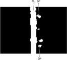
도 1a는 레이저 빔이 가공대상물의 내부에 집광되어 이동하면서 개질 영역을 형성하는 모습을 도시한 것이다.
도 1b 및 도 1c는 도 1a에서 레이저 빔이 개질 영역의 주위로 스플래쉬되는 모습을 도시한 것이다.
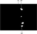
도 2a 및 도 2b는 가공대상물에 부착된 이미지 필름에 형성된 레이저 스플래쉬에 의한 가공대상물의 손상 이미지를 찍은 사진이다.
도 3은 본 발명의 예시적인 실시예에 따른 레이저 가공장비의 자동 검사 장치를 개략적으로 도시한 것이다.
도 4는 도 3에 도시된 가공대상물 및 가공대상물의 하면에 코팅된 이미지 필름을 도시한 것이다.
도 5는 본 발명의 예시적인 실시예에 따른 레이저 가공장비의 자동 검사 장치를 개략적으로 도시한 것이다.
도 6a 내지 도 6d는 자동 검사 장치의 이미지 처리부가 이미지 필름에 형성된 가공대상물의 손상 이미지를 처리하는 과정을 도시한 것이다.
도 7은 이미지 필름에 찍힌 손상 포인트들에 대한 위치 정보를 추출하는 방법을 예시적으로 보여주는 도면이다.1A shows a state in which a laser beam is condensed in an object to be processed and moves to form a modified region.
Figs. 1B and 1C show a state in which the laser beam is splashed around the modified region in Fig. 1A.
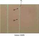
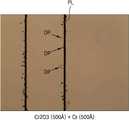
2A and 2B are photographs showing damage images of an object to be processed by laser splash formed on an image film attached to the object to be processed.
3 schematically shows an automatic inspection apparatus for laser processing equipment according to an exemplary embodiment of the present invention.
Fig. 4 shows an image film coated on the lower surface of the object to be processed and the object shown in Fig. 3;
5 schematically shows an automatic inspection apparatus for laser processing equipment according to an exemplary embodiment of the present invention.
6A to 6D illustrate a process of processing a damaged image of an object to be processed formed on an image film by the image processing unit of the automatic inspection apparatus.
FIG. 7 is an exemplary view showing a method of extracting positional information on damage points imprinted on an image film.
이하, 첨부된 도면을 참조하여 본 발명의 실시예를 상세히 설명한다. 아래에 예시되는 실시예는 본 발명의 범위를 한정하는 것은 아니며, 본 발명을 이 기술 분야에서 통상의 지식을 가진 자에게 설명하기 위해서 제공되는 것이다. 도면에서 동일한 참조부호는 동일한 구성요소를 지칭하며, 각 구성요소의 크기나 두께는 설명의 명료성을 위하여 과장되어 있을 수 있다. 또한, 소정의 물질층이 예를 들어 기판에 존재한다고 설명될 때, 그 물질층은 기판에 직접 접하면서 존재할 수도 있고, 그 사이에 다른 제3의 층이 존재할 수도 있다. 그리고, 아래의 실시예에서 각 구성요소를 이루는 물질은 예시적인 것이므로, 이외에 다른 물질이 사용될 수도 있다.Hereinafter, embodiments of the present invention will be described in detail with reference to the accompanying drawings. The embodiments illustrated below are not intended to limit the scope of the invention, but rather are provided to illustrate the invention to those skilled in the art. In the drawings, like reference numerals refer to like elements, and the size and thickness of each element may be exaggerated for clarity of explanation. Also, when it is described that a given material layer is present, for example, on a substrate, the material layer may be present in direct contact with the substrate, and there may be another third layer in between. In the following embodiments, the materials constituting each component are illustrative, and other materials may be used.
도 1a는 레이저 빔(L)이 가공대상물(W)의 내부에 집광되어 이동하면서 개질 영역(도 1b의 20)을 형성하는 모습을 도시한 것이다.FIG. 1A shows a state in which a laser beam L is condensed in the interior of the object W and moves to form a modified region (20 in FIG. 1B).
도 1a를 참조하면, 레이저 가공장비로부터 출사된 레이저 빔(L)이 가공대상물(W)의 내부에 집속됨으로써 집광점(10)을 형성하게 된다. 여기서, 레이저 빔(L)은 가공대상물(W)의 상면 쪽에서 가공대상물(W)의 내부로 입사될 수 있다. 이러한 가공대상물(W)은 레이저 빔(L)에 대해 투과성을 가지는 물질로 이루어질 수 있다. 예를 들어 가공대상물(W)은 반도체 웨이퍼가 될 수 있지만, 이에 한정되는 것은 아니다. 그리고, 가공대상물(W)의 내부에 집광점(10)을 형성하기 위한 레이저 빔(L)으로는 짧은 펄스폭(예를 들면, 피코초(pico second) 또는 나노초(nano second) 범위의 펄스폭)을 가지는 레이저 빔이 사용될 수 있다.1A, a laser beam L emitted from a laser processing machine is focused on an object W to form a light-
이와 같이, 가공대상물(W)의 내부에 레이저 빔(L)이 집속되어 집광점(10)을 형성하게 되면 이 집광점(10)과 그 주위에는 개질 영역(20)이 형성되고, 이러한 개질 영역(20)으로부터 그 주위로 크랙이 연장되어 형성될 수 있다. 그리고, 레이저 빔(L)을 가공 라인(PL)을 따라 움직이게 되면 가공대상물(W)의 내부에는 가공라인(PL)을 따라 개질 영역(20)이 연장되어 형성될 수 있다. 도 1a는 레이저 빔(L)이 x방향을 따라 이동하면서 개질 영역(20)을 형성하는 모습이 예시적으로 도시되어 있다.As described above, when the laser beam L is focused on the object W to form the light-converging
도 1b 및 도 1c는 도 1a에서 레이저 빔(L)이 개질 영역(20)에 중첩되면서 개질 영역(20)의 주위로 스플래쉬되는 모습을 도시한 것이다. 구체적으로, 도 1b는 도 1a에서 B-B'선을 따라 본 단면도이며, 도 1c는 도 1a에서 C-C'선을 따라 본 단면도이다.1B and 1C show a state in which the laser beam L is splashed around the modified
도 1b 및 도 1c를 참조하면, 가공대상물(W)의 상면 쪽에서 레이저 빔이 입사하여 가공대상물(W)의 내부에 형성된 개질 영역(20)을 만나게 되면 간섭에 의해 레이저 빔(L)이 그 주위로 스플래쉬(splash)되는 현상이 발생될 수 있다. 이렇게 스플래쉬된 레이저 빔들(SL)은 가공대상물(W)의 하면 쪽으로 진행하면서 가공대상물(W)의 하부를 손상시킬 수 있다. 이에 따라, 가공대상물(W)의 하면에는 스플래쉬된 레이저 빔들(SL)에 의해 가공대상물(W)이 손상된 지점들을 나타내는 손상 포인트들(damage point, DP)이 생성될 수 있다.1B and 1C, when a laser beam is incident on the upper surface of the object to be processed W and the modified
도 1b에는 레이저 빔(L)이 가공 라인(PL), 즉 x방향을 따라 이동하는 과정에서 x방향 또는 -x방향으로 스플래쉬되는 레이저 빔들(SL)에 의해 가공대상물(W)의 하면에 형성된 손상 포인트들(DP)이 도시되어 있으며, 도 1c에는 레이저 빔(L)이 가공 라인(PL), 즉 x방향을 따라 이동하는 과정에서 x방향에 수직한 방향인 y방향 또는 -y방향으로 스플래쉬되는 레이저빔들(SL)에 의해 가공대상물(W)의 하면에 형성된 손상 포인트들(DP)이 도시되어 있다.1B shows a state in which the laser beam SL is splashed in the x direction or the -x direction in the process of moving the laser beam L along the processing line PL, 1C shows a state in which the laser beam L is splashed in the y direction or the -y direction perpendicular to the x direction in the process of moving along the processing line PL, that is, the x direction The damage points DP formed on the lower surface of the object W by the laser beams SL are shown.
도 1b에 도시된 바와 같이, 가공 라인(PL)에 나란한 방향(즉, x방향 또는 -x방향)으로 스플래쉬된 레이저빔들(SL)에 의해 가공대상물(W)이 손상되어 형성된 손상 포인트들(DP)은 가공대상물(W)이 가공 라인(P)을 따라 절단되는 경우에 가공 품질에 큰 영향을 주지 않을 수 있다. 그러나, 도 1c에 도시된 바와 같이, 가공 라인에 수직한 방향(즉, y방향 또는 -y방향)으로 스플래쉬된 레이저 빔들(SL)에 의해 가공대상물(W)이 손상됨으로써 형성된 손상 포인트들(DP)은 가공 품질에 나쁜 영향을 줄 수 있다. 구체적인 예를 들면, 가공대상물(W)이 소자들이 집적된 반도체 웨이퍼인 경우 가공 라인(PL)에 수직한 방향으로 스플래쉬된 레이저 빔들(SL)은 소자들이 위치한 액티브 영역(active area)에 영향을 줄 수 있으며, 이 경우에는 반도체 칩이 손상을 받을 수 있다.As shown in Fig. 1B, the object W is damaged by the laser beams SL splashed in the direction parallel to the processing line PL (i.e., the x direction or the -x direction) DP may not have a great influence on the processing quality when the object W is cut along the processing line P. [ However, as shown in Fig. 1C, the damage points DP formed by damaging the object W by the laser beams SL splashed in the direction perpendicular to the processing line (i.e., the y direction or the -y direction) ) May adversely affect the machining quality. For example, when the object W is a semiconductor wafer on which elements are integrated, the laser beams SL splashed in the direction perpendicular to the processing line PL affect the active area in which the elements are located In this case, the semiconductor chip may be damaged.
도 2a 및 도 2b는 실리콘 웨이퍼에 가공작업을 수행한 다음, 실리콘 웨이퍼의 하면에 부착된 이미지 필름에 나타난 손상 포인트들을 찍은 사진이다. 여기서, 레이저 빔은 실리콘 웨이퍼의 상면으로부터 그 내부에 집속되어 개질 영역을 형성하면서 가공라인을 따라 이동하였으며, 이미지 필름에는 개질 영역과 만나면서 스플래쉬된 레이저 빔들이 실리콘 웨이퍼의 하부를 투과한 다음 실리콘 웨이퍼의 하면에 부착된 이미지 필름과 반응하면서 형성된 손상 포인트들이 형성되어 있다.2A and 2B are photographs showing damage points appearing on an image film attached to a lower surface of a silicon wafer after a processing operation is performed on the silicon wafer. Here, the laser beam is focused from the upper surface of the silicon wafer to the inner side of the silicon wafer while moving along the processing line while forming the modified region, and splashed laser beams are transmitted through the lower portion of the silicon wafer, Damage points formed while reacting with the image film attached to the lower surface are formed.
도 2a의 경우에는 실리콘 웨이퍼의 하면에 500Å두께의 카본으로 이루어진 이미지 필름이 부착되었으며, 도 2b의 경우에는 실리콘 웨이퍼의 하면에 500Å 두께의 크롬 산화물 및 500Å 두께의 크롬으로 이루어진 이미지 필름을 부착되었다. 도 2a 및 도 2b에 도시된 바와 같이, 스플래쉬된 레이저 빔들에 의해 가공대상물이 손상되어 가공대상물의 하면에는 가공라인과 수직한 방향으로 가공대상물의 손상된 지점들을 나타내는 다수의 손상 포인트들이 생성되었음을 알 수 있다.2A, an image film made of carbon having a thickness of 500 A was attached to the lower surface of the silicon wafer. In FIG. 2B, an image film made of chromium oxide having a thickness of 500 A and chromium having a thickness of 500A was attached to the lower surface of the silicon wafer. As shown in FIGS. 2A and 2B, it can be seen that the object is damaged by the splashed laser beams, and a plurality of damage points are generated on the lower surface of the object, which indicate damaged points of the object in a direction perpendicular to the processing line have.
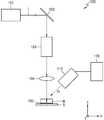
도 3은 본 발명의 예시적인 실시예에 따른 레이저 가공장비의 자동 검사 장치(100)를 개략적으로 도시한 것이다. 도 3에는 가공대상물(W)의 내부에 레이저 빔(L)을 조사하여 개질 영역(20)을 형성하는 레이저 가공장비의 가공 품질을 검사하는 자동 검사 장치(100)가 도시되어 있다. 그리고, 도 4에는 도 3에 도시된 가공대상물(W) 및 가공대상물(W)의 하면에 코팅된 이미지 필름(150)이 도시되어 있다.3 schematically shows an
도 3 및 도 4를 참조하면, 자동 검사 장치(100)는 가공대상물(W)의 하면에 코팅된 이미지 필름(image film, 150)과, 레이저 가공에 의해 이미지 필름(150)에 형성되는 손상 이미지(damage image)를 검출하는 이미지 검출부(image sensing unit, 110)와, 이미지 검출부(110)에 의해 검출된 손상 이미지를 처리하는 이미지 처리부(image processing unit, 120)를 포함할 수 있다.3 and 4, the
가공대상물(W)에 레이저 빔(L)을 조사하여 가공작업을 수행하는 레이저 가공장비에서는 광원(101)으로부터 레이저 빔(L)이 출사되고, 이렇게 출사된 레이저 빔(L)은 소정의 미러(102)를 통해 반사된 다음, 소정 광학계(103)를 경유할 수 있다. 여기서, 광학계(103)에는 예를 들면 BET(Beam Expanding Telescope), 스캔 광학계 등이 포함될 수 있지만, 이에 한정되는 것은 아니다. 그리고, 광학계(103)를 나온 레이저 빔(L)은 집속 렌즈(104)에 의해 집속되어 가공대상물(W)의 내부에 조사될 수 있다.The laser beam L is emitted from the
레이저 빔(L)은 가공대상물(W)의 상면 쪽에서 내부로 입사되어 집광점을 형성할 수 있다. 여기서, 레이저 빔(L)은 예를 들면, 피코초(pico second) 또는 나노초(nano second) 범위의 짧은 펄스폭을 가질 수 있다. 가공대상물(W)은 레이저 빔에 대해 투과성을 가지는 물질로 이루어질 수 있다. 예를 들면, 가공대상물(W)은 반도체 웨이퍼를 포함할 수 있다. 이 경우, 반도체 웨이퍼의 하면에 소자들이 집적되어 있을 수 있다. 하지만, 이는 단지 예시적인 것으로 이외에도 가공대상물(W)은 다른 다양한 재질을 포함할 수 있다.The laser beam L is incident on the upper side of the object W to form a light-converging point. Here, the laser beam L may have a short pulse width in the range of, for example, pico second or nano second. The object W may be made of a material having transparency to the laser beam. For example, the object to be processed W may include a semiconductor wafer. In this case, the elements may be integrated on the lower surface of the semiconductor wafer. However, this is merely exemplary and the object W may include other various materials.
가공대상물(W)의 하면에는 이미지 필름(150)이 코팅되어 있다. 이미지 필름(150)은 후술하는 레이저 스플래쉬에 의해 가공대상물(W)이 손상된 부분들을 나타내기 위한 것이다. 이러한 이미지 필름(150)은 가공대상물(W)의 내부에 조사되는 레이저 빔(L)과 반응성을 가지는 물질로 이루어질 수 있다. 예를 들면, 이미지 필름(150)은 카본, 크롬 및 크롬 산화물 중 적어도 하나를 포함할 수 있다. 하지만, 이는 단지 예시적인 것으로 레이저 빔(L)의 종류에 따라 이미지 필름(150)을 구성하는 물질은 다양하게 변형될 수 있다.An
가공대상물(W)의 주위에는 이미지 검출부(110)가 마련되어 있다. 이미지 검출부(110)는 가공대상물(W)에 측정빔을 조사하여 가공대상물(W)의 하면에 코팅된 이미지 필름에 형성된 손상 이미지를 검출하기 위한 것이다. 이를 위해 이미지 검출부(110)는 가공대상물(W)을 투과하여 이미지 필름(150)에 형성된 손상 이미지를 촬영할 수 있는 측정빔을 방출하는 카메라가 사용될 수 있다. 예를 들면, 이미지 검출부(110)로는 적외선(IR)을 방출하는 적외선 카메라(IR camera)가 사용될 수 있다. 하지만 이는 단지 예시적인 것으로 이미지 검출부(110)는 이외에도 다양한 파장 범위의 측정빔을 방출하는 카메라를 포함할 수 있다.An
한편, 이미지 필름(150)에 형성되는 손상 이미지를 명확하게 찍기 위해서는 이미지 검출부(110)로부터 방출되는 측정빔의 파장에 따라 이미지 필름(150)을 구성하는 물질이 달라질 수 있다. 예를 들어, 이미지 검출부(110)로부터 방출되는 측정빔이 적외선인 경우에는 이미지 필름(150)으로는 카본 필름 보다는 크롬 및/또는 크롬 산화물로 이루어진 필름이 사용될 수 있다.The material constituting the
본 실시예에서 이미지 검출부(110)는 레이저 가공장비와 가공대상물(W)을 정렬(alignment)하는데 사용되는 카메라로도 사용될 수 있다. 이 경우, 이미지 검출부(110)는 레이저 가공장비와 가공대상물(W)을 원하는 위치에 올바르게 정렬하는 동시에 레이저 가공 후 이미지 필름(150)에 형성된 손상 이미지를 검출하는데 사용될 수 있다.In this embodiment, the
이미지 처리부(120)는 이미지 검출부(110)로부터 검출된 손상 이미지를 처리하는 역할을 한다. 구체적으로, 이미지 처리부(120)는 이미지 필름(150)에 형성된 손상 이미지를 이진화 이미지로 변경하고, 이 이진화 이지미로부터 가공라인 이미지를 제거한 다음, 가공대상물이 손상된 부분을 나타내는 손상 포인트들(damage points)에 대한 위치 정보를 추출하게 된다.The
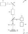
도 5는 본 발명의 다른 예시적인 실시예에 따른 레이저 가공장비의 자동 검사 장치(200)를 개략적으로 도시한 것이다. 도 5에 도시된 자동 검사 장치(200)는 이미지 검출부(110)로부터 방출된 측정빔(예를 들면, IR)이 다이크로익 미러(dichroic mirror)에 의해 반사된 다음 레이저 빔(L)이 진행하는 경로를 따라 가공대상물(W)에 조사된다는 점을 제외하면 도 3에 도시된 자동 검사 장치(100)와 그 구성이 동일하다.5 schematically shows an
이하에서는 도 3 및 도 5에 도시된 레이저 가공장비의 자동 검사 장치(100,200)를 이용하여 레이저 가공장비의 가공 품질을 자동적으로 검사하는 방법에 대해 설명한다.Hereinafter, a method of automatically checking the processing quality of the laser processing equipment using the
스테이지(S) 상에 이미지 필름(150)이 코팅된 가공대상물(W)을 적재한다. 여기서, 이미지 필름(150)은 가공대상물(W)의 하면에 코팅될 수 있다. 가공대상물(W)로는 예를 들어 하면에 소자들이 집적된 실리콘 웨이퍼가 사용될 수 있지만, 이에 한정되는 것은 아니다.The object W on which the
다음으로, 레이저 가공장비를 이용하여 가공대상물(W)에 대해 가공작업을 수행한다. 구체적으로, 레이저 가공장비로부터 출사된 레이저 빔(L)은 가공대상물(W)의 상면 쪽에서 조사되며, 이렇게 조사된 레이저 빔(L)은 가공대상물(W)의 내부에 집속되어 집광점을 형성한다. 이와 같이, 가공대상물(W)의 내부에 집광점이 형성되면 집광점과 그 주위에는 개질 영역(20)이 형성될 수 있으며, 이러한 개질 영역(20)으로부터 주위로 크랙이 연장되어 발생할 수 있다. 그리고, 레이저 빔(L)을 가공 라인(PL)을 따라 움직이게 되면 가공대상물(W)의 내부에는 가공 라인(PL)을 따라 개질 영역(20)이 연장되어 형성될 수 있다.Next, a machining operation is performed on the object W using a laser processing equipment. More specifically, the laser beam L emitted from the laser processing equipment is irradiated from the upper surface side of the object W, and the laser beam L thus irradiated is focused on the object W to form a light-converging point . Thus, when the light-converging point is formed in the object W, the light-converging point and the modified
한편, 가공작업을 수행하는 과정에서 가공대상물(W)의 내부에 조사되는 레이저 빔(L)이 개질 영역(20)과 중첩되면 간섭에 의해 개질 영역(20) 주위로 레이저 빔(L)이 스플래쉬될 수 있으며, 이렇게 스플래쉬된 레이저 빔들(SL)은 가공대상물(W)의 하면 쪽으로 진행하면서 가공대상물(W)의 하부를 손상시킬 수 있다. 이에 따라, 가공대상물(W)의 하면에는 스플래쉬된 레이저 빔들(SL)에 의해 가공대상물(W)이 손상된 지점들을 나타내는 손상 포인트들(DP)이 생성될 수 있다. 도 4에는 레이저 빔(L)이 y방향을 따라 이동하면서 가공작업을 수행하고, y방향에 수직한 방향으로 스플래쉬된 레이저 빔들(SL)에 의해 이미지 필름(150)에 형성된 손상 포인트들(DP)이 예시적으로 도시되어 있다.Meanwhile, when the laser beam L irradiated inside the object W is overlapped with the modified
이어서, 이미지 검출부(110)가 레이저 가공작업 중에 가공대상물(W)의 하면에 코팅된 이미지 필름(150)에 형성된 가공대상물(W)의 손상 이미지를 검출한다. 여기서, 이미지 필름(150)에 형성된 손상 이미지는 레이저 가공작업 중에 가공대상물(W) 내부에서 개질 영역(20)에 의해 스플래쉬된 레이저 빔들(SL)이 가공대상물(W)의 하면으로부터 나오면서 이미지 필름(150)과 반응하여 형성된 것이다. 따라서, 이미지 필름(150)에 형성된 손상 이미지로부터 가공대상물(W)의 하면이 스플래쉬된 레이저 빔(SL)에 의해 손상된 상태를 알 수 있다. 도 6a에는 이미지 검출부(110)에 의해 검출된 이미지 필름(150)의 손상 이미지가 예시적으로 도시되어 있다.Then, the
다음으로, 이미지 처리부(120)가 이미지 검출부(110)에 의해 검출된 손상 이미지를 처리한다. 이미지 처리부(120)는 이미지 필름(150)에 형성된 손상 이미지를 이진화 이미지로 변경하고, 이 이진화 이지미로부터 가공라인 이미지를 제거한 다음, 가공대상물(W)이 손상된 부분을 나타내는 손상 포인트들(DP)에 대한 위치 정보를 추출하게 된다.Next, the
이미지 검출부(110)에 의해 검출된 가공대상물(W)의 손상 이미지를 이미지 처리부(120)에 의해 처리하는 구체적인 과정은 도 6a 내지 도 6d를 참조하여 설명한다. 여기서, 도 6a 내지 도 6d에 도시된 결과에서는 가공대상물(W)로는 실리콘 웨이퍼를 사용하였으며, 이미지 필름(150)으로는 크롬 및 크롬 산화물로 이루어진 필름을 사용하였다. 그리고, 사용된 레이저 빔(L)의 파장은 1083nm, 펄스폭은 350ns 이었다.A detailed process of processing the image of damage of the object W detected by the
도 6a에는 이미지 검출부(110, 적외선 카메라)에 의해 찍힌 이미지 필름(150)의 손상 이미지가 도시되어 있다. 도 6a를 참조하면, 레이저 빔(L)이 가공 라인(PL)을 따라 이동한 모습을 보여주는 가공 라인(PL) 이미지와 가공 라인(PL) 주변에 스플래쉬된 레이저 빔들(SL)에 의해 형성된 손상 포인트들(DP)이 도시되어 있다.6A shows a damaged image of the
이미지 처리부(120)는 먼저, 이미지 검출부(110)에 의해 검출된 가공대상물(W)의 손상 이미지를 이진화 이미지로 변경한다. 여기서, 이진화 이미지는 손상 이미지를 2개의 밝기로 표현한 이미지를 의미한다. 도 6b에는 도 6a에 도시된 가공대상물(W)의 손상 이미지를 이진화 이미지로 변경한 모습이 도시되어 있다.The
다음으로, 이미지 처리부(110)는 이진화 이미지로부터 레이저 빔(L)이 이동한 가공 라인(PL) 이미지를 제거한다. 도 6c에는 도 6b에 도시된 이진화 이미지로부터 가공라인(PL) 이미지가 제거된 모습이 도시되어 있다.Next, the
이어서, 이미지 처리부(120)는 가공 라인(PL) 이미지가 제거된 상태에서 가공대상물(W)의 손상된 지점들을 나타내는 손상 포인트들(DP)에 대한 위치 정보를 추출한다. 이를 위해서는 가공라인(PL) 이미지가 제거된 이진화 이미지에서 센터 라인(CL)을 설정한 다음, 이 센터 라인(CL)을 기준으로 손상 포인트들(DP)의 거리를 측정한다. 도 6d에는 가공라인(PL) 이미지가 제거된 이진화 이미지에서 센터 라인(CL)을 설정한 모습이 도시되어 있다.Subsequently, the
이하에서는 손상 포인트들에 대한 위치 정보를 추출하는 방법을 도 7을 참조하여 보다 구체적으로 설명한다. 도 7에는 이미지 필름(150)에 찍힌 손상 포인트들(DP1~DP9)에 대한 위치 정보를 추출하는 방법이 예시적으로 도시되어 있다.Hereinafter, a method of extracting the location information on the damage points will be described in more detail with reference to FIG. FIG. 7 exemplarily shows a method of extracting position information on the damage points DP1 to DP9 imaged on the
도 7를 참조하면, 가공 라인(PL) 이미지가 제거된 상태에서 이진화 이미지에 센터 라인(CL)을 설정한다. 여기서, 센터 라인(CL)은 가공 라인(PL)의 중심선을 따라 설정될 수 있다. 그리고, 이러한 센터 라인(CL)의 주위에는 가공대상물(W)의 손상된 지점들을 나타내는 손상 포인트들(DP1~DP9)이 형성되어 있다. 도 7에는 9개의 손상 포인트들(DP1~DP9)이 예시적으로 도시되어 있다.Referring to FIG. 7, the center line CL is set in the binarized image with the processing line (PL) image removed. Here, the center line CL can be set along the center line of the processing line PL. Damage points DP1 to DP9 indicating the damaged points of the object W are formed around the center line CL. In Fig. 7, nine damage points DP1 to DP9 are illustrated by way of example.
이와 같이 센터 라인(CL)을 설정한 다음, 이 센터 라인(CL)과 손상 포인트들(DP1~DP9) 사이의 거리들(d1~d9)을 각각 측정한다. 그리고, 이렇게 측정된 거리값들(d1~d9)을 데이터로 만들어 저장한다.After setting the center line CL in this way, the distances d1 to d9 between the center line CL and the damage points DP1 to DP9 are respectively measured. Then, the measured distance values d1 to d9 are stored as data.
이상과 같이, 센터 라인(CL)과 손상 포인트들(DP) 사이의 거리들(d1~d9)을 모두 측정하여 데이터로 저장한 다음, 이 데이터를 토대한 하여 레이저 가공장비의 가공 품질을 파악한다. 도 7에서 WD는 가공작업에서 손상이 허용될 수 있는 가공폭을 나타낸다. 따라서, 가공폭(WD) 내에 위치하는 손상 포인트들(DP1,DP3,DP4,DP6,DP9)은 가공에 의해 제거될 수 있는 것이므로 레이저 가공장비의 가공 품질에 영향을 주지 않을 수 있다. 그러나, 가공폭(WD)을 벗어나는 손상 포인트들(DP2,DP5,DP7,DP8)은 예를 들어 소자들이 집적된 반도체 웨이퍼의 액티브 영역 등에 손상을 줄 수 있는 것으로 이는 레이저 가공장비의 가공 품질에 영향을 줄 수 있다. 따라서, 이미지 처리부(120)를 통해 손상 포인트들(DP1~DP9)에 대한 위치 정보, 즉 센터 라인과 손상 포인트들 사이의 거리들을 추출함으로써 레이저 가공장비의 가공 품질을 자동적으로 파악할 수 있게 된다.As described above, all of the distances d1 to d9 between the center line CL and the damage points DP are measured and stored as data, and the machining quality of the laser processing equipment is grasped based on this data . In Fig. 7, WD represents the machining width at which damage can be tolerated in the machining operation. Therefore, the damage points DP1, DP3, DP4, DP6, and DP9 located within the machining width WD can be removed by machining, so that the machining quality of the laser machining equipment may not be affected. However, the damage points DP2, DP5, DP7, and DP8 that deviate from the processing width WD can damage, for example, the active area of the semiconductor wafer on which the devices are integrated, . Accordingly, the
이와 같이, 본 실시예에 따른 자동 검사 장치(100,200)는 스테이지(S)에 가공대상물(W)을 적재한 다음, 레이저 가공장비에 의해 가공대상물(W)을 가공하는 과정, 이미지 검출부(110)가 이미지 필름(150)에 형성된 손상 이미지를 검출하는 과정 및 이미지 처리부(120)가 손상 포인트들(DP)에 대한 위치 정보(즉, 센터 라인과 손상 포인트들 사이의 거리들)를 추출하는 과정을 모두 자동적으로 진행하여 레이저 가공장비의 가공 품질을 검사할 수 있다. 이에 따라, 레이저 가공장비에 대한 현 상태를 미리 파악할 수 있으며, 그 결과 원하는 가공 품질을 얻을 수 있도록 레이저 가공장비에 대한 수선 및 관리를 용이하게 할 수 있다. 그리고, 레이저 가공장비의 정렬에 사용되는 카메라를 이미지 검출부(110)로 그대로 사용함으로써 장치를 보다 간단하게 구성할 수 있다. 또한, 레이저 가공작업 후 가공대상물(W)을 스테이지(S)로부터 분리하지 않고 스테이지(S)에 적재된 상태에서 가공대상물(W)의 손상 이미지를 이미지 검출부(110)가 검출함으로써 보다 간단한 공정으로 레이저 가공장비의 가공 품질을 파악할 수 있다. 이상에서 본 발명의 실시예가 설명되었으나, 이는 예시적인 것에 불과하며, 당해 분야에서 통상적 지식을 가진 자라면 이로부터 다양한 변형 및 균등한 타 실시예가 가능하다는 점을 이해할 것이다.As described above, the
10.. 집광점
20.. 개질영역
100,200.. 레이저 가공장비의 자동 검사 장치
101.. 광원
102.. 반사미러
103.. 광학계
104.. 집속 렌즈
110.. 이미지 검출부
120.. 이미지 처리부
150.. 이미지 필름
PL.. 가공 라인
CL.. 센터 라인
S.. 스테이지
W.. 가공대상물10 .. condensing point
20. Modification zone
100,200 .. Automatic inspection system of laser processing equipment
101 .. Light source
102 .. reflection mirror
103 .. Optical system
104. Focusing lens
110. Image detector
120,
150 .. Image film
PL .. processing line
CL .. Center Line
S .. Stage
W .. The object to be processed
Claims (21)
Translated fromKorean상기 가공대상물의 하면에 코팅되는 이미지 필름(image film);
상기 레이저 빔의 조사에 의해 상기 이미지 필름에 형성된 상기 가공대상물의 손상 이미지(damage image)를 검출하는 이미지 검출부(image sensing unit); 및
상기 이미지 검출부에 의해 검출된 손상 이미지를 처리하는 이미지 처리부(image processing unit);를 포함하는 레이저 가공 장비의 자동 검사 장치.An apparatus for inspecting a machining quality of a laser machining apparatus for forming a modified region by irradiating a laser beam inside a workpiece,
An image film coated on the lower surface of the object to be processed;
An image sensing unit for detecting a damage image of the object formed on the image film by irradiation of the laser beam; And
And an image processing unit for processing the damaged image detected by the image detecting unit.
상기 레이저 빔은 상기 가공대상물의 상면 쪽에 입사되어 상기 가공대상물의 내부에 개질 영역을 형성하는 레이저 가공 장비의 자동 검사 장치.The method according to claim 1,
Wherein the laser beam is incident on an upper surface side of the object to form a modified region inside the object.
상기 가공대상물은 반도체 웨이퍼를 포함하는 레이저 가공 장비의 자동 검사 장치.The method according to claim 1,
Wherein the object to be processed comprises a semiconductor wafer.
상기 이미지 필름은 상기 레이저 빔과 반응성을 가지는 물질을 포함하는 레이저 가공 장비의 자동 검사 장치.The method according to claim 1,
Wherein the image film comprises a material reactive with the laser beam.
상기 이미지 필름은 카본, 크롬 및 크롬 산화물 중 적어도 하나를 포함하는 레이저 가공 장비의 자동 검사 장치.5. The method of claim 4,
Wherein the image film comprises at least one of carbon, chromium and chromium oxide.
상기 가공대상물의 손상 이미지는 상기 레이저 빔이 상기 개질 영역의 주변으로 스플래쉬(splash)되어 상기 이미지 필름과 반응하면서 형성되는 레이저 가공 장비의 자동 검사 장치.5. The method of claim 4,
Wherein the damage image of the object to be processed is formed while the laser beam is splashed to the periphery of the modified region and reacted with the image film.
상기 이미지 검출부는 상기 가공대상물을 투과하는 측정빔을 이용하여 상기이미지 필름에 형성된 상기 손상 이미지를 검출하는 레이저 가공 장비의 자동 검사 장치.The method according to claim 6,
Wherein the image detecting unit detects the damaged image formed on the image film using a measurement beam transmitted through the object.
상기 이미지 검출부는 상기 레이저 가공장비와 상기 가공대상물의 정렬(alignment)에 사용되는 카메라를 포함하는 레이저 가공 장비의 자동 검사 장치.8. The method of claim 7,
Wherein the image detection unit includes a camera used for alignment of the laser processing equipment and the object to be processed.
상기 이미지 검출부는 적외선 카메라(IR camera)를 포함하는 레이저 가공 장비의 자동 검사 장치.8. The method of claim 7,
Wherein the image detecting unit includes an infrared camera (IR camera).
상기 이미지 처리부는 상기 손상 이미지를 이진화 이미지로 변경하고, 상기 이진화 이미지로부터 가공라인 이미지를 제거한 다음, 상기 가공대상물이 손상된 지점들을 나타내는 손상 포인트들(damage points)의 위치 정보를 추출하는 레이저 가공 장비의 자동 검사 장치.The method according to claim 1,
Wherein the image processing unit changes the damaged image to a binarized image, removes a machining line image from the binarized image, and extracts position information of damage points indicating points where the object is damaged Automatic inspection device.
이미지 필름에 코팅된 상기 가공대상물을 준비하는 단계;
상기 레이저 가공장비를 이용하여 상기 레이저 빔을 상기 가공대상물의 내부에 조사하여 가공작업을 진행하는 단계;
상기 레이저 빔의 조사에 의해 상기 이미지 필름에 형성된 상기 가공대상물의 손상 이미지를 검출하는 단계; 및
상기 가공대상물의 손상 이미지를 처리하는 단계;를 포함하는 레이저 가공 장비의 자동 검사 방법.A method for inspecting a machining quality of a laser machining apparatus for forming a modified region by irradiating a laser beam inside a workpiece,
Preparing the object to be processed coated on the image film;
Irradiating the inside of the object with the laser beam using the laser processing equipment to advance a machining operation;
Detecting a damaged image of the object formed on the image film by irradiation of the laser beam; And
And processing the damaged image of the object to be inspected.
상기 이미지 필름은 상기 가공대상물의 하면에 코팅되고, 상기 레이저 빔은 상기 가공대상물의 상면 쪽에 입사되어 상기 가공대상물의 내부에 개질 영역을 형성하는 레이저 가공 장비의 자동 검사 방법.12. The method of claim 11,
Wherein the image film is coated on a lower surface of the object to be processed and the laser beam is incident on an upper surface side of the object to form a modified region inside the object.
상기 이미지 필름은 상기 레이저 빔과 반응성을 가지는 물질을 포함하는 레이저 가공 장비의 자동 검사 방법.12. The method of claim 11,
Wherein the image film comprises a material reactive with the laser beam.
상기 가공대상물의 손상 이미지는 상기 레이저 빔이 상기 개질 영역의 주변으로 스플래쉬(splash)되어 상기 이미지 필름과 반응하면서 형성되는 레이저 가공 장비의 자동 검사 방법.14. The method of claim 13,
Wherein the damage image of the object to be processed is formed while the laser beam is splashed to the periphery of the modified region and reacted with the image film.
상기 이미지 필름에 형성된 상기 가공대상물의 손상 이미지는 이미지 검출부에 의해 검출되는 레이저 가공 장비의 자동 검사 방법.12. The method of claim 11,
Wherein the damage image of the object formed on the image film is detected by an image detection unit.
상기 이미지 검출부는 상기 가공대상물을 투과하는 측정빔을 이용하여 상기이미지 필름에 형성된 상기 손상 이미지를 검출하는 레이저 가공 장비의 자동 검사 방법.16. The method of claim 15,
Wherein the image detecting unit detects the damaged image formed on the image film using a measuring beam transmitted through the object.
상기 이미지 검출부는 상기 레이저 가공장비와 상기 가공대상물의 정렬에 사용되는 카메라를 포함하는 레이저 가공 장비의 자동 검사 방법.16. The method of claim 15,
Wherein the image detecting unit includes a camera used for aligning the laser processing equipment with the object to be processed.
상기 가공대상물의 손상 이미지는 이미지 처리부에 의해서 처리되는 레이저 가공 장비의 자동 검사 방법.16. The method of claim 15,
Wherein the damaged image of the object is processed by an image processing unit.
상기 가공대상물의 손상 이미지를 처리하는 단계는,
상기 이미지 검출부에 의해 검출된 상기 가공대상물의 손상 이미지를 이진화 이미지로 변경하는 단계;
상기 이진화 이미지로부터 가공라인 이미지를 제거하는 단계; 및
상기 가공라인 이미지가 제거된 상기 이진화 이미지에서 상기 가공대상물이 손상된 지점들을 나타내는 손상 포인트들의 위치 정보를 추출하는 단계;를 포함하는 레이저 가공 장비의 자동 검사 방법.19. The method of claim 18,
Wherein the step of processing the damaged image of the object comprises:
Changing a damaged image of the object detected by the image detecting unit to a binarized image;
Removing a machining line image from the binarized image; And
And extracting positional information of damage points indicating points where the object is damaged in the binarized image from which the machining line image has been removed.
상기 손상 포인트들의 위치 정보를 추출하는 단계는,
상기 이진화 이미지에 센터 라인(center line)을 설정하는 단계; 및
상기 센터 라인과 상기 손상 포인트들 사이의 거리를 측정하여 데이터로 저장하는 단계;를 포함하는 레이저 가공 장비의 자동 검사 방법.20. The method of claim 19,
Wherein the step of extracting the location information of the damage points comprises:
Setting a center line in the binarized image; And
Measuring a distance between the center line and the damage points and storing the data as data.
상기 데이터를 토대로 상기 레이저 가공 장비의 가공 품질을 파악하는 단계를 더 포함하는 레이저 가공 장비의 자동 검사 방법.21. The method of claim 20,
Further comprising the step of grasping the processing quality of the laser processing equipment based on the data.
Priority Applications (5)
| Application Number | Priority Date | Filing Date | Title |
|---|---|---|---|
| KR1020150145432AKR101716369B1 (en) | 2015-10-19 | 2015-10-19 | Auto inspection apparatus and method of laser processing apparatus |
| PCT/KR2016/009010WO2017069388A1 (en) | 2015-10-19 | 2016-08-17 | Automatic inspection device and method of laser processing equipment |
| US15/757,500US10770298B2 (en) | 2015-10-19 | 2016-08-17 | Automatic inspection device and method of laser processing equipment |
| CN201680053556.4ACN108140589B (en) | 2015-10-19 | 2016-08-17 | Automatic inspection device and method for laser processing equipment |
| TW105126974ATWI595230B (en) | 2015-10-19 | 2016-08-24 | Auto inspection apparatus and method of laser processing apparatus |
Applications Claiming Priority (1)
| Application Number | Priority Date | Filing Date | Title |
|---|---|---|---|
| KR1020150145432AKR101716369B1 (en) | 2015-10-19 | 2015-10-19 | Auto inspection apparatus and method of laser processing apparatus |
Publications (1)
| Publication Number | Publication Date |
|---|---|
| KR101716369B1true KR101716369B1 (en) | 2017-03-27 |
Family
ID=58496666
Family Applications (1)
| Application Number | Title | Priority Date | Filing Date |
|---|---|---|---|
| KR1020150145432AActiveKR101716369B1 (en) | 2015-10-19 | 2015-10-19 | Auto inspection apparatus and method of laser processing apparatus |
Country Status (5)
| Country | Link |
|---|---|
| US (1) | US10770298B2 (en) |
| KR (1) | KR101716369B1 (en) |
| CN (1) | CN108140589B (en) |
| TW (1) | TWI595230B (en) |
| WO (1) | WO2017069388A1 (en) |
Families Citing this family (3)
| Publication number | Priority date | Publication date | Assignee | Title |
|---|---|---|---|---|
| JP6797481B2 (en)* | 2017-03-01 | 2020-12-09 | 株式会社ディスコ | Semiconductor ingot inspection method, inspection equipment and laser processing equipment |
| JP7112204B2 (en)* | 2018-02-07 | 2022-08-03 | 株式会社ディスコ | Nondestructive detection method |
| JP7665345B2 (en)* | 2021-01-29 | 2025-04-21 | 浜松ホトニクス株式会社 | Observation device and observation method |
Citations (4)
| Publication number | Priority date | Publication date | Assignee | Title |
|---|---|---|---|---|
| JP2008055455A (en)* | 2006-08-30 | 2008-03-13 | Sumitomo Electric Ind Ltd | Laser processing method and laser processing apparatus |
| KR20140140206A (en)* | 2013-05-28 | 2014-12-09 | 주식회사 이오테크닉스 | Laser processing apparatus and laser processing method |
| KR20150065917A (en)* | 2000-09-13 | 2015-06-15 | 하마마츠 포토닉스 가부시키가이샤 | Cutting method, cutting method for workpiece, and cutting method for optically transparent material |
| KR20160089277A (en)* | 2015-01-19 | 2016-07-27 | 가부시기가이샤 디스코 | Method for testing laser beam |
Family Cites Families (8)
| Publication number | Priority date | Publication date | Assignee | Title |
|---|---|---|---|---|
| WO2007005636A2 (en)* | 2005-06-30 | 2007-01-11 | Controlled Semiconductor, Inc. | Semiconductor failure analysis tool |
| JP2007035133A (en)* | 2005-07-26 | 2007-02-08 | Sony Corp | Lens position control method, lens position controller, cutting method, and cutting device |
| JP4988224B2 (en)* | 2006-03-01 | 2012-08-01 | 株式会社日立ハイテクノロジーズ | Defect inspection method and apparatus |
| JP2009061744A (en)* | 2007-09-07 | 2009-03-26 | Sony Corp | Manufacturing equipment for laminated products |
| JP5331421B2 (en)* | 2008-09-12 | 2013-10-30 | オリンパス株式会社 | Laser repair device and laser repair method |
| KR101076455B1 (en)* | 2010-02-17 | 2011-10-25 | 주식회사 이오테크닉스 | Method for detecting area processed with a laser |
| JP2013176788A (en)* | 2012-02-28 | 2013-09-09 | Olympus Corp | Laser processing apparatus, laser processing method and laser processing program |
| CN107074633B (en)* | 2014-10-22 | 2019-12-27 | 日本板硝子株式会社 | Method for producing glass substrate and plate-shaped glass |
- 2015
- 2015-10-19KRKR1020150145432Apatent/KR101716369B1/enactiveActive
- 2016
- 2016-08-17WOPCT/KR2016/009010patent/WO2017069388A1/ennot_activeCeased
- 2016-08-17USUS15/757,500patent/US10770298B2/enactiveActive
- 2016-08-17CNCN201680053556.4Apatent/CN108140589B/enactiveActive
- 2016-08-24TWTW105126974Apatent/TWI595230B/enactive
Patent Citations (4)
| Publication number | Priority date | Publication date | Assignee | Title |
|---|---|---|---|---|
| KR20150065917A (en)* | 2000-09-13 | 2015-06-15 | 하마마츠 포토닉스 가부시키가이샤 | Cutting method, cutting method for workpiece, and cutting method for optically transparent material |
| JP2008055455A (en)* | 2006-08-30 | 2008-03-13 | Sumitomo Electric Ind Ltd | Laser processing method and laser processing apparatus |
| KR20140140206A (en)* | 2013-05-28 | 2014-12-09 | 주식회사 이오테크닉스 | Laser processing apparatus and laser processing method |
| KR20160089277A (en)* | 2015-01-19 | 2016-07-27 | 가부시기가이샤 디스코 | Method for testing laser beam |
Also Published As
| Publication number | Publication date |
|---|---|
| WO2017069388A1 (en) | 2017-04-27 |
| TW201715223A (en) | 2017-05-01 |
| TWI595230B (en) | 2017-08-11 |
| CN108140589B (en) | 2022-04-29 |
| CN108140589A (en) | 2018-06-08 |
| US20180247818A1 (en) | 2018-08-30 |
| US10770298B2 (en) | 2020-09-08 |
Similar Documents
| Publication | Publication Date | Title |
|---|---|---|
| KR102235580B1 (en) | Defect marking for semiconductor wafer inspection | |
| JP5469839B2 (en) | Device surface defect inspection apparatus and method | |
| CN107305863B (en) | wafer processing method | |
| JP6465722B2 (en) | Processing equipment | |
| CN105382420B (en) | Laser processing device | |
| TWI630967B (en) | Laser processing device | |
| US9285211B2 (en) | Height detecting apparatus | |
| KR102231739B1 (en) | Method of inspecting laser beam | |
| KR20160002353A (en) | Laser machining apparatus | |
| KR101716369B1 (en) | Auto inspection apparatus and method of laser processing apparatus | |
| KR20190047550A (en) | Laser processing method, substrate dicing method, and substrate processing apparatus for performing the same | |
| KR102866847B1 (en) | Laser machining method and laser machining apparatus | |
| JP5420890B2 (en) | Device for measuring the height position of the workpiece held on the chuck table | |
| JP7313128B2 (en) | IMAGING DEVICE, LASER PROCESSING DEVICE, AND IMAGING METHOD | |
| US8502988B2 (en) | Pattern inspection apparatus and pattern inspection method | |
| CN105643118A (en) | Detection method of transmission laser beam | |
| CN108376665B (en) | processing method | |
| JPWO2022181301A5 (en) | ||
| JP5656690B2 (en) | Laser processing equipment | |
| KR20140140206A (en) | Laser processing apparatus and laser processing method | |
| JP2009115611A (en) | Inspection apparatus for electronic element | |
| JP7138417B2 (en) | Foreign Matter Inspection Apparatus, Foreign Matter Inspection Method, Imprint Apparatus, and Article Manufacturing Method | |
| KR20210066846A (en) | Imaging apparatus, laser processing apparatus, and imaging method | |
| TW202203307A (en) | Wafer inspection method | |
| US20250153278A1 (en) | Processing method and processing system |
Legal Events
| Date | Code | Title | Description |
|---|---|---|---|
| PA0109 | Patent application | Patent event code:PA01091R01D Comment text:Patent Application Patent event date:20151019 | |
| PA0201 | Request for examination | ||
| E701 | Decision to grant or registration of patent right | ||
| PE0701 | Decision of registration | Patent event code:PE07011S01D Comment text:Decision to Grant Registration Patent event date:20170307 | |
| GRNT | Written decision to grant | ||
| PR0701 | Registration of establishment | Comment text:Registration of Establishment Patent event date:20170308 Patent event code:PR07011E01D | |
| PR1002 | Payment of registration fee | Payment date:20170309 End annual number:3 Start annual number:1 | |
| PG1601 | Publication of registration | ||
| FPAY | Annual fee payment | Payment date:20200310 Year of fee payment:4 | |
| PR1001 | Payment of annual fee | Payment date:20200310 Start annual number:4 End annual number:4 | |
| PR1001 | Payment of annual fee | Payment date:20210309 Start annual number:5 End annual number:5 | |
| PR1001 | Payment of annual fee | Payment date:20220310 Start annual number:6 End annual number:6 | |
| PR1001 | Payment of annual fee | Payment date:20240307 Start annual number:8 End annual number:8 |