KR101715331B1 - Communication transceiver for vehicular selectively using a plurality of communication method - Google Patents
Communication transceiver for vehicular selectively using a plurality of communication methodDownload PDFInfo
- Publication number
- KR101715331B1 KR101715331B1KR1020160006670AKR20160006670AKR101715331B1KR 101715331 B1KR101715331 B1KR 101715331B1KR 1020160006670 AKR1020160006670 AKR 1020160006670AKR 20160006670 AKR20160006670 AKR 20160006670AKR 101715331 B1KR101715331 B1KR 101715331B1
- Authority
- KR
- South Korea
- Prior art keywords
- communication
- bit stream
- digital bit
- lin
- signal
- Prior art date
- Legal status (The legal status is an assumption and is not a legal conclusion. Google has not performed a legal analysis and makes no representation as to the accuracy of the status listed.)
- Active
Links
Images


Classifications
- H—ELECTRICITY
- H04—ELECTRIC COMMUNICATION TECHNIQUE
- H04L—TRANSMISSION OF DIGITAL INFORMATION, e.g. TELEGRAPHIC COMMUNICATION
- H04L12/00—Data switching networks
- H04L12/28—Data switching networks characterised by path configuration, e.g. LAN [Local Area Networks] or WAN [Wide Area Networks]
- H04L12/40—Bus networks
- H04L12/40006—Architecture of a communication node
- H04L12/40039—Details regarding the setting of the power status of a node according to activity on the bus
- H—ELECTRICITY
- H04—ELECTRIC COMMUNICATION TECHNIQUE
- H04L—TRANSMISSION OF DIGITAL INFORMATION, e.g. TELEGRAPHIC COMMUNICATION
- H04L12/00—Data switching networks
- H04L12/28—Data switching networks characterised by path configuration, e.g. LAN [Local Area Networks] or WAN [Wide Area Networks]
- H04L12/40—Bus networks
- H04L2012/40208—Bus networks characterized by the use of a particular bus standard
- H04L2012/40215—Controller Area Network CAN
- H—ELECTRICITY
- H04—ELECTRIC COMMUNICATION TECHNIQUE
- H04L—TRANSMISSION OF DIGITAL INFORMATION, e.g. TELEGRAPHIC COMMUNICATION
- H04L12/00—Data switching networks
- H04L12/28—Data switching networks characterised by path configuration, e.g. LAN [Local Area Networks] or WAN [Wide Area Networks]
- H04L12/40—Bus networks
- H04L2012/40208—Bus networks characterized by the use of a particular bus standard
- H04L2012/40234—Local Interconnect Network LIN
- H—ELECTRICITY
- H04—ELECTRIC COMMUNICATION TECHNIQUE
- H04L—TRANSMISSION OF DIGITAL INFORMATION, e.g. TELEGRAPHIC COMMUNICATION
- H04L12/00—Data switching networks
- H04L12/28—Data switching networks characterised by path configuration, e.g. LAN [Local Area Networks] or WAN [Wide Area Networks]
- H04L12/40—Bus networks
- H04L2012/40267—Bus for use in transportation systems
- H04L2012/40273—Bus for use in transportation systems the transportation system being a vehicle
Landscapes
- Engineering & Computer Science (AREA)
- Computer Networks & Wireless Communication (AREA)
- Signal Processing (AREA)
- Small-Scale Networks (AREA)
Abstract
Translated fromKoreanDescription
Translated fromKorean본 발명은 차량용 통신 송수신기에 관한 것으로, 상세하게는 서로 다른 통신 방식을 수행하는 복수의 통신 모듈이 원 칩(1-chip) 형태로 구현되도록 하되 입출력 버스 라인(Bus Line) 또한 공용으로 사용할 수 있도록 설계함으로써, 버스 라인들과 연결되는 입출력 단자의 수를 줄이고 칩 사이즈의 이득을 볼 수 있도록 한 복수의 통신 방식을 선택적으로 이용하는 차량용 통신 송수신기에 관한 것이다.The present invention relates to a vehicular communication transceiver, and more particularly, to a vehicular communication transceiver that allows a plurality of communication modules performing different communication methods to be implemented in a one-chip form, but also allows an input / output bus line to be shared And more particularly, to a vehicle communication transceiver that selectively uses a plurality of communication methods for reducing the number of input / output terminals connected to bus lines and for obtaining a gain of a chip size.
일반적으로, 차량용 통신 시스템들은 다른 전자 제품들에 비해 상대적으로 단순한 버스 시스템이 통신 규약에 따라 적용된다. 구체적으로, 하나의 전송 라인만을 포함하는 LIN 버스(Local Interconnect Network Bus)를 비롯하여, 2개 정도로 되도록 적은 수의 버스 라인들을 이용하는 CAN_HIGH, CAN_LOW, 및 CAN_GND(ground) 등의 CAN 버스(Controller Area Network Bus) 등이 이용된다.In general, automotive communication systems are applied in accordance with communication protocols in a relatively simple bus system as compared to other electronic products. Specifically, a CAN bus such as CAN_HIGH, CAN_LOW, and CAN_GND (ground) using as few as two bus lines, including a Local Interconnect Network Bus (LIN) bus including only one transmission line, ) Are used.
이와 더불어, 데이터 전송속도를 더욱 향상시키기 위해, 대한민국 등록특허공보 제10-1519793호(2015. 2. 6 등록)에는 CAN FD(CAN flexible data rate) 프로토콜이 제시 및 적용되기도 하였다. CAN FD 프로토콜에 따르면, CAN 프레임의 실제 유용한 데이터는 CAN 2.0프로토콜에서 정의된 것보다 높은 전송 속도로 전송된다.In addition, in order to further improve the data transmission speed, CAN flexible data rate (CAN FD) protocol has been proposed and applied to Korean Patent Registration No. 10-1519793 (registered on Feb. 2, 2015). According to the CAN FD protocol, the actual useful data of the CAN frame is transmitted at a higher transmission rate than that defined in the CAN 2.0 protocol.
상술한 바와 같이, LIN 통신 모듈은 하나의 전송 라인만을 사용하고, CAN 통신 모듈은 HIGH, LOW 및 GND(ground) 전송라인을 사용한다. 그리고, 전송 속도 또한 LIN, CAN, CAN FD 통신 모듈이 모두 서로 달라 LIN, CAN, CAN FD 통신 모듈을 서로 혼용하여 사용할 수는 없다.As described above, the LIN communication module uses only one transmission line, and the CAN communication module uses HIGH, LOW and GND (ground) transmission lines. Also, the LIN, CAN, and CAN FD communication modules are different from each other, and the LIN, CAN, and CAN FD communication modules can not be used in combination.
근래에는, LIN 통신 모듈과 CAN 통신 모듈을 하나의 칩에 집적하여 원 칩 형태로 구현하고자 하는 노력이 있었으나, 이 또한 원 칩 구조라 할지라도 각각의 통신 모듈별로 서로 다른 버스 라인을 통해 서로 다른 전송 속도로 통신을 수행하도록 설계된바, 칩 사이즈가 커지고 입출력 단자 및 연결된 버스 라인의 수가 줄지 않아 원 칩의 의미가 크게 퇴색되는 문제가 있었다.In recent years, efforts have been made to integrate a LIN communication module and a CAN communication module into a single chip so as to implement it in a one-chip form. However, even in a one-chip structure, The chip size is increased and the number of the input / output terminals and the number of the connected bus lines is not reduced, so that the meaning of the original chip is greatly deteriorated.
상기와 같은 문제점을 해결하기 위한 본 발명의 목적은 LIN, CAN, CAN FD 통신 모듈 등과 같이 서로 다른 통신 방식을 수행하는 복수의 통신 모듈이 원 칩(1-chip) 형태로 구현되도록 하되, 입출력 버스 라인 또한 공용으로 사용할 수 있도록 설계함으로써, 버스 라인 및 버스 라인들과 연결되는 입출력 단자의 수를 줄이고 칩 사이즈의 이득을 볼 수 있도록 한 복수의 통신 방식을 선택적으로 이용하는 차량용 통신 송수신기를 제공하는 것이다.In order to solve the above-mentioned problems, an object of the present invention is to provide a communication system in which a plurality of communication modules performing different communication methods such as LIN, CAN, and CAN FD communication modules are implemented in a one-chip form, Lines are also designed to be commonly used so as to provide a vehicle communication transceiver selectively using a plurality of communication methods for reducing the number of input / output terminals connected to bus lines and bus lines and for obtaining gain of chip size.
상기와 같은 목적을 달성하기 위한 본 발명의 실시 예에 따른 복수의 통신 방식을 선택적으로 이용하는 차량용 통신 송수신기는 외부 마이크로 프로세서로부터의 디지털 코드나 신호를 CAN, LIN, CAN FD 중 미리 설정된 통신 방식의 디지털 비트 스트림으로 전송하는 하는 제어신호 생성부, 전송되는 디지털 비트 스트림의 속도를 검출하고 검출 결과에 따라 상기의 CAN, LIN, CAN FD 통신 방식 중 어느 한 통신 방식으로 디지털 비트 스트림이 전송되도록 적어도 하나의 출력 노드를 선택하여 출력하는 신호 검출 판단부, 및 신호 검출 판단부의 선택 노드에 따라 CAN, LIN, CAN FD 통신 모듈 중 어느 한 통신 모듈만을 활성화시켜 CAN, LIN, CAN FD 통신 방식 중 활성화된 통신 방식으로 디지털 비트 스트림을 적어도 하나의 버스 라인으로 송출하는 통합 통신 모듈부를 포함한다.According to another aspect of the present invention, there is provided a vehicle communication transceiver for selectively using a plurality of communication methods according to an exemplary embodiment of the present invention. The communication transceiver includes a CAN, a LIN, and a CAN A control signal generator for detecting the speed of the digital bit stream to be transmitted and for transmitting the digital bit stream through one of the CAN, LIN and CAN FD communication methods according to the detection result, LIN, and CAN FD communication modules by activating only one of CAN, LIN, and CAN FD communication modules according to the selection node of the signal detection determination unit, And an integrated communication module unit for transmitting the digital bit stream to at least one bus line The.
상기에서 설명한 본 발명의 복수의 통신 방식을 선택적으로 이용하는 차량용 통신 송수신기에 의하면 LIN, CAN, CAN FD 통신 모듈 등과 같이 서로 다른 통신 방식을 수행하는 복수의 통신 모듈이 원 칩(1-chip) 형태로 구현되도록 하되, 입출력 버스 라인 또한 공용으로 사용할 수 있도록 설계함으로써, 버스 라인 및 버스 라인들과 연결되는 입출력 단자의 수를 줄이고 칩 사이즈의 이득을 볼 수 있는 효과가 있다.According to the vehicle communication transceiver selectively using the plurality of communication methods of the present invention as described above, a plurality of communication modules performing different communication methods such as LIN, CAN, and CAN FD communication modules are formed in a one-chip form And the input / output bus line is also designed to be commonly used, thereby reducing the number of input / output terminals connected to the bus line and the bus line, and achieving a gain in chip size.
또한, 하나의 칩 형태로 구현된 통합 송수신기 구조에 의해 한 번의 패키징 과정을 통해 CAN 통신과 LIN 통신 및 CAN FD 통신 송수신기를 통합해서 사용할 수 있게 되어 비용적인 면에서 이득을 얻게 된다.In addition, the integrated transceiver structure implemented in a single chip forms a single packaging process, which enables the CAN communication, the LIN communication, and the CAN FD communication transceiver to be integrated, thereby achieving a cost advantage.
또한, PCB 기판에 패키징 된 칩을 배치하는데 필요한 면적에 이득을 보게 되어 PCB의 라우팅 라인의 여유를 얻을 수 있게 된다.In addition, the area required to place the packaged chips on the PCB substrate is advantageous, and the margin of the routing line of the PCB can be obtained.
특히, LIN 통신을 위한 TRX로 동작시킬 경우 하나의 칩을 가지고 2개의 버스 노드를 제어할 수 있는데, 하나의 노드에 물린 최대 16개의 클러스터를 8개의 패키징 된 칩으로 제어할 수 있다.In particular, when operating as TRX for LIN communication, two bus nodes can be controlled with one chip, and up to 16 clusters banged on one node can be controlled by 8 packaged chips.
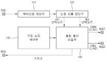
도 1은 본 발명의 실시 예에 따른 복수의 통신 방식을 선택적으로 이용하는 차량용 통신 송수신기를 나타낸 회로 블록도이다.
도 2는 도 1에 도시된 구동모드 제어부와 통합 통신 모듈부 구성을 구체적으로 나타낸 회로 블록도이다.
도 3은 도 2에 도시된 통합 통신 모듈부 구성을 더욱 구체적으로 나타낸 회로 블록도이다.1 is a circuit block diagram showing a vehicle communication transceiver selectively using a plurality of communication methods according to an embodiment of the present invention.
FIG. 2 is a circuit block diagram specifically illustrating the configuration of the driving mode control unit and the integrated communication module unit shown in FIG. 1. Referring to FIG.
3 is a circuit block diagram showing the configuration of the integrated communication module unit shown in FIG. 2 in more detail.
이하, 본 발명의 실시 예를 첨부한 도면들을 참조하여 상세히 설명하기로 한다.Hereinafter, embodiments of the present invention will be described in detail with reference to the accompanying drawings.
마이크로 프로세서(예를 들어, ECU)에서 통신 송수신기의 입력단인 TXD 단으로 디지털 신호를 전송하면 전송된 신호는 출력 버스 라인으로 출력되되, 이때 출력되는 같은 위상을 가진 전송 신호는 마이크로 프로세서의 피드백 신호(F/D_S) 입력단인 RXD 단으로 피드백되어 전송된 신호(F/D_S)의 출력을 확인할 수 있도록 하는 데이터 패스(Data Path) 구조가 차량용 통신 송수신기의 신호 송출 구조이다.When a digital signal is transmitted from a microprocessor (for example, an ECU) to a TXD terminal, which is an input terminal of a communication transceiver, the transmitted signal is output to an output bus line. F / D_S) is fed back to the RXD stage and the output of the transmitted signal (F / D_S) is verified by the signal transmission structure of the vehicular communication transceiver.
예를 들어, CAN 통신 방식이나 LIN 방식 또는 CAN FD 통신 방식에 따른 국제표준화기구(International Organization for Standardization) 규격에 맞는 디지털 비트 스트림을 마이크로 프로세서에서 전달해 주면 CAN 송수신기(Transceiver)나 LIN 송수신기에서 신호를 받아 출력 버스 라인으로 전달해주는 방식이다. 이를 위해 CAN, LIN, CAN FD 등의 차량 통신에 따른 국제표준화기구 규격에서 요구하는 파라미터들은 CAN, LIN, CAN FD 등의 통신 송수신기에서 만족시켜야 한다.For example, if a microprocessor transmits a digital bitstream conforming to the International Organization for Standardization (CAN) standard, the CAN protocol, the LIN protocol, or the CAN FD protocol, a CAN transceiver or a LIN transceiver receives a signal To the output bus line. For this purpose, the parameters required by the International Standardization Organization Specification for CAN, LIN, CAN FD, etc. for vehicle communication must be satisfied by communication transceivers such as CAN, LIN, and CAN FD.
본 발명에서는 LIN, CAN, CAN FD 통신 모듈 등과 같이 서로 다른 통신 방식을 수행하는 복수의 통신 모듈이 원 칩(1-chip) 형태로 구현되도록 하되, 입출력 버스 라인 또한 공용으로 사용할 수 있도록 설계한다.In the present invention, a plurality of communication modules performing different communication methods such as LIN, CAN, and CAN FD communication modules are implemented in a one-chip form, and input / output bus lines are also designed to be commonly used.
도 1은 본 발명의 실시 예에 따른 복수의 통신 방식을 선택적으로 이용하는 차량용 통신 송수신기를 나타낸 회로 블록도이다.1 is a circuit block diagram showing a vehicle communication transceiver selectively using a plurality of communication methods according to an embodiment of the present invention.
먼저, 도 1에 도시된 차량용 통신 송수신기는 제어신호 생성부(111), 신호 검출 판단부(121), 구동 모드 제어부(131), 통합 통신 모듈부(141)를 포함하여 구성된다.1 includes a control
도시되지 않은 마이크로 프로세서(예를 들어, ECU)에서 차량용 통신 송수신기의 제어신호 생성부(111) 입력단인 TXD 단으로 디지털 신호를 전송하면 전송된 신호는 최종 출력단인 통합 통신 모듈부(141)의 출력 버스 라인으로 출력되되, 이때 출력되는 전송 신호는 마이크로 프로세서의 피드백 신호(F/D_S) 입력단인 RXD 단으로 피드백되어, 신호 검출 판단부(121)는 피드백되는 전송 신호(F/D_S)의 출력을 확인하는 데이터 패스 구조를 이룬다.When a digital signal is transmitted from an unillustrated microprocessor (for example, an ECU) to a TXD terminal, which is an input terminal of the
구체적으로, 제어신호 생성부(111)는 외부의 마이크로 프로세서 등으로부터의 디지털 코드나 신호를 CAN, LIN, CAN FD 중 미리 설정된 통신 방식의 디지털 비트 스트림으로 전송한다.Specifically, the control
제어신호 생성부(111)의 입력단은 마이크로 프로세서 등의 외부 프로세서 출력단인 TXD 단과 연결된다. 이에, 제어신호 생성부(111)는 마이크로 프로세서 등으로부터 CAN, LIN, CAN FD 중 미리 설정된 통신 방식에 따른 디지털 코드나 신호를 입력받는다. 그리고, 입력된 디지털 코드나 신호를 디지털 비트 스트림(bitstream) 형태로 신호 검출 판단부(121)에 공급한다.The input terminal of the
신호 검출 판단부(121)는 전송되는 디지털 비트 스트림의 속도를 검출하고 검출 결과에 따라 상기의 CAN, LIN, CAN FD 통신 방식 중 어느 한 통신 방식으로 디지털 비트 스트림이 전송되도록 적어도 하나의 출력 노드를 선택하여 출력한다.The signal
구체적으로, 신호 검출 판단부(121)는 외부의 마이크로 프로세서 및 제어신호 생성부(111)를 통해 입력되는 디지털 비트 스트림의 속도를 인식하여 CAN, LIN, CAN FD 통신 방식 중 어떤 통신 방식으로 통신이 수행되는지를 판단한다. 예를 들어, 입력되는 디지털 비트 스트림의 속도가 LIN 표준 통신 방식에 해당하여 20kbps이나, 10.4kbps 등과 같은 속도로 판단되면 LIN 통신 방식으로 판단한다. 그리고, 상기의 디지털 비트 스트림을 LIN 통신 노드로 출력함으로써 통합 통신 모듈부(141)의 LIN 통신 모듈을 활성화시킨다.Specifically, the signal
반면, 신호 검출 판단부(121)는 입력되는 디지털 비트 스트림의 속도가 CAN 표준 통신 방식에 해당하는 125kbps 내지 1Mbps 중 어느 한 속도로 판단되면 CAN 통신 방식으로 판단한다. 이에, 신호 검출 판단부(121)는 상기의 디지털 비트 스트림을 CAN 통신 노드로 출력함으로써 통합 통신 모듈부(141)의 CAN 통신 모듈을 활성화시키게 된다.On the other hand, if the speed of the input digital bit stream is determined to be any one of 125 kbps to 1 Mbps corresponding to the CAN standard communication method, the signal
한편, 신호 검출 판단부(121)는 입력되는 디지털 비트 스트림의 속도가 CAN 2.0 프로토콜에서 정의된 것보다 높은 전송 속도로 판단되면 CAN FD 통신 방식으로 판단한다. 이에, 신호 검출 판단부(121)는 상기의 디지털 비트 스트림을 CAN FD 통신 노드로 출력함으로써, 통합 통신 모듈부(141)의 CAN FD 통신 모듈을 활성화시킬 수도 있다.On the other hand, if the rate of the input digital bit stream is determined to be higher than that defined in the CAN 2.0 protocol, the signal
통합 통신 모듈부(141)는 신호 검출 판단부(121)의 선택 노드에 따라 CAN, LIN, CAN FD 통신 모듈 중 어느 한 통신 모듈만을 활성화시켜 CAN, LIN, CAN FD 통신 방식 중 활성화된 통신 방식으로 디지털 비트 스트림을 적어도 하나의 버스 라인(BUS1, BUS2)으로 송출한다.The integrated
구체적으로, 통합 통신 모듈부(141)에는 CAN, LIN, CAN FD 통신 모듈 중 복수의 통신 모듈에 집적화되어 구성될 수 있다. 이하에서는 설명의 편의상 CAN 통신 모듈과 LIN 통신 모듈에 집적화되어 구동되는 예를 설명하기로 한다. 이에, 신호 검출 판단부(121)로부터 디지털 비트 스트림이 LIN 통신 노드로 입력되면, 통합 통신 모듈부(141)의 LIN 통신 모듈이 활성화되어 LIN 통신 방식으로 디지털 비트 스트림을 적어도 하나의 버스 라인(BUS1, BUS2)으로 송출한다.Specifically, the integrated
반면, 신호 검출 판단부(121)로부터 디지털 비트 스트림이 CAN 통신 노드로 입력되면, 통합 통신 모듈부(141)의 CAN 통신 모듈이 활성화되어 CAN 통신 방식으로 디지털 비트 스트림을 적어도 하나의 버스 라인(BUS1, BUS2)으로 송출한다. 이때, 통합 통신 모듈부(141)에 집적된 LIN 통신 모듈과 CAN 통신 모듈은 버스 라인(BUS1, BUS2)들을 공유한다. 이러한, 통합 통신 모듈부(141)에 대해서는 추 후에 첨부된 도면을 참조하여 좀 더 구체적으로 설명하기로 한다.On the other hand, when the digital bit stream is input from the signal
구동 모드 제어부(131)는 마이크로 프로세서의 제어에 따라 전력 소모를 줄이기 위한 모드 제어 신호 예를 들어, Wake up signal, Sleep Signal, Enable Signal, Disable Signal 중 적어도 하나의 신호를 생성하여 모드 제어 신호를 디지털 비트 스트림 형태로 상기 제어신호 생성부(111) 또는 통합 통신 모듈부(141)로 제공한다. 이에, 제어신호 생성부(111)나 통합 통신 모듈부(141)는 CAN, LIN, CAN FD 중 미리 설정된 통신 방식에 따른 디지털 비트 스트림 형태로 Wake up signal, Sleep Signal, Enable Signal, Disable Signal 중 적어도 하나의 신호를 출력하게 된다.The drive
도 2는 도 1에 도시된 구동모드 제어부와 통합 통신 모듈부 구성을 구체적으로 나타낸 회로 블록도이다.FIG. 2 is a circuit block diagram specifically illustrating the configuration of the driving mode control unit and the integrated communication module unit shown in FIG. 1. Referring to FIG.
도 2에 도시된 바와 같이, 구동 모드 제어부(131)는 전원 공급부(132), 모드 제어부(133), 및 보호 회로부(134)를 포함하여 구성된다.2, the driving
구체적으로, 전원 공급부(132)는 차량용 송수신기 자체 구동에 필요한 바이어스 전압 및 전류를 생성 및 제공한다. 그리고, 모드 제어부(133)는 Wake up, Sleep, Standby 모드 전환에 따른 모드 제어 신호로 Wake up signal, Sleep Signal, Enable Signal, Disable Signal 중 적어도 하나의 신호를 생성하여 디지털 비트 스트림 형태로 제어신호 생성부(111) 또는 통합 통신 모듈부(141)로 제공하게 된다.Specifically, the
보호 회로부(134)는 고전압 및 ESD 방지 보호 회로를 포함하되 CAN 버스의 커먼 모드(Common mode) 전압을 생성하여 통합 통신 모듈부(141)의 CAN 통신 모듈(142)로 제공한다.The
통합 통신 모듈부(141)는 도 2에 도시된 바와 같이, 신호 검출 판단부(121)로부터 디지털 비트 스트림이 CAN 통신 노드로 입력되면 활성화되어 CAN 통신 방식으로 디지털 비트 스트림을 복수의 버스 라인(BUS1, BUS2)으로 송출하는 CAN 통신 모듈(142), 및 신호 검출 판단부(121)로부터의 디지털 비트 스트림이 LIN 통신 노드로 입력되면 활성화되어 LIN 통신 방식으로 디지털 비트 스트림을 적어도 하나의 버스 라인(BUS1, BUS2)으로 송출하는 LIN 통신 모듈(143)을 포함하여 구성된다.2, the integrated
한편, 통합 통신 모듈부(141)에는 신호 검출 판단부(121)로부터 디지털 비트 스트림이 CAN FD 통신 노드로 입력되면 활성화되어 CAN FD 통신 방식으로 디지털 비트 스트림을 복수의 버스 라인(BUS1, BUS2)으로 송출하는 CAN FD 통신 모듈을 더 구비하여 구성되기도 한다. 이에, 통합 통신 모듈부(141)에 집적된 LIN 통신 모듈(143)과 CAN 통신 모듈(142) 및 CAN FD 통신 모듈은 버스 라인(BUS1, BUS2)들을 공유하여 각기의 통신 방식으로 디지털 비트 스트림을 출력하게 된다.When the digital bit stream is input to the CAN FD communication node from the signal
도 3은 도 2에 도시된 통합 통신 모듈부 구성을 더욱 구체적으로 나타낸 회로 블록도이다.3 is a circuit block diagram showing the configuration of the integrated communication module unit shown in FIG. 2 in more detail.
도 3을 참조하면, CAN 통신 모듈(142)은 신호 검출 판단부(121)로부터의 디지털 비트 스트림에 응답하여 턴-온 또는 턴-오프 됨으로써 CAN 통신 방식으로 CANH 비트의 디지털 비트 스트림을 제 1 버스 라인(BUS1)으로 송출하는 적어도 하나의 제 1 스위칭 소자(Tr1), 및 신호 검출 판단부(121)로부터의 디지털 비트 스트림에 응답하여 턴-온 또는 턴-오프 됨으로써 CAN 통신 방식으로 CANL 비트의 디지털 비트 스트림을 제 2 버스 라인(BUS2)으로 송출하는 적어도 하나의 제 2 스위칭 소자(Tr2)를 포함하여 구성된다. 여기서, CANH 또는 CANL 비트의 디지털 비트 스트림은 커먼 모드(Common mode) 전압을 기준으로 각각 하이 또는 로우 상태로 구분되어 출력되는 신호이다.Referring to FIG. 3, the
한편, 제 1 및 제 2 스위칭 소자(Tr1,Tr2) 각각은 PMOS 및 NMOS 중 적어도 하나의 POWER MOSFET가 될 수 있는데, 본 발명에서는 제 1 스위칭 소자(Tr1)가 PMOS POWER MOSFET로 구성되고 제 2 스위칭 소자(Tr2)는 NMOS POWER MOSFET로 구성된 예를 도시한다. 여기서, 제 1 스위칭 소자(Tr1)의 소스 단자는 전류 공급원인 VDD와 연결되며, 제 2 스위칭 소자(Tr2)의 소스 단자는 그라운드 또는 접지단인 GND와 연결될 수 있다.Each of the first and second switching elements Tr1 and Tr2 may be a power MOSFET of at least one of PMOS and NMOS. In the present invention, the first switching element Tr1 is a PMOS POWER MOSFET and the second switching The element Tr2 is an example configured of an NMOS POWER MOSFET. Here, the source terminal of the first switching device Tr1 is connected to the power supply source VDD, and the source terminal of the second switching device Tr2 is connected to the ground or the ground GND.
이때 제 1 및 제 2 스위칭 소자(Tr1,Tr2) 각각은 LIN 통신 모듈(143)에서 출력되는 12V 이상의 전압 스윙을 견뎌낼 수 있도록 설계 및 형성되어야 한다. 만일, 어느 한 POWER MOSFET의 드레인(Drain) 전극이 공정상에서 protection layer를 보강하지 않은 일반적인 CAN 통신 모듈(142)에 사용하는 소자를 선정한다면 LIN 통신 방식으로 사용하고 난 후에는 소자가 망가져 버려 CAN 통신 모듈(142)로 더 이상 사용할 수 없게 된다.At this time, each of the first and second switching elements Tr1 and Tr2 must be designed and formed so as to withstand a voltage swing of 12 V or more output from the
도 3에 도시된 바와 같이, LIN 통신 모듈(143)은 신호 검출 판단부(121)로부터의 디지털 비트 스트림에 응답하여 턴-온 또는 턴-오프 됨으로써 LIN 통신 방식으로 비트의 디지털 비트 스트림을 제 1 버스 라인(BUS1)으로 송출하는 적어도 하나의 제 3 스위칭 소자(Tr3), 및 신호 검출 판단부(121)로부터의 디지털 비트 스트림에 응답하여 턴-온 또는 턴-오프 됨으로써 LIN 통신 방식으로 디지털 비트 스트림을 제 2 버스 라인(BUS2)으로 송출하는 적어도 하나의 제 4 스위칭 소자(Tr4)를 포함하여 구성된다.3, the
구체적으로, 제 3 및 제 4 스위칭 소자(Tr3,Tr4) 각각은 PMOS 및 NMOS 중 적어도 하나의 POWER MOSFET가 될 수 있는데, 본 발명에서는 제 3 및 제 4 스위칭 소자(Tr3,Tr4)가 모두 NMOS POWER MOSFET로 구성된 예를 도시한다. 여기서, 제 3 및 제 4 스위칭 소자(Tr3,Tr4)의 소스 단자는 그라운드 또는 접지단인 GND와 연결될 수 있다. 이에, 제 3 및 제 4 스위칭 소자(Tr3,Tr4)는 턴-온 또는 턴-오프되어, 제 1 버스 라인(BUS1)으로의 LIN1 신호와 제 2 버스 라인(BUS2)으로의 LIN2 신호가 동일한 위상의 신호로 출력된다. 이렇게 구성된 LIN 통신 방식의 경우에는 출력단 출력 노드가 제 3 스위칭 소자(Tr3)와 제 4 스위칭 소자(Tr4)의 드레인 단이 되며, CAN 통신 모듈(142) 제 1 및 제 2 스위칭 소자(Tr1,Tr2)의 드레인 단과 각각 노드를 공유하게 된다.Specifically, each of the third and fourth switching elements Tr3 and Tr4 may be a power MOSFET of at least one of a PMOS and an NMOS. In the present invention, the third and fourth switching elements Tr3 and Tr4 are all NMOS POWER MOSFET. Here, the source terminals of the third and fourth switching elements Tr3 and Tr4 may be connected to a ground or GND which is a ground terminal. The third and fourth switching elements Tr3 and Tr4 are turned on or turned off so that the LIN1 signal to the first bus line BUS1 and the LIN2 signal to the second bus line BUS2 are in the same phase As shown in FIG. In the case of the LIN communication system configured as described above, the output stage output node is the drain terminal of the third switching device Tr3 and the fourth switching device Tr4, and the
이상 상술한 구성에 의해, 본 발명의 복수의 통신 방식을 선택적으로 이용하는 차량용 통신 송수신기는 LIN, CAN, CAN FD 통신 모듈 등과 같이 서로 다른 통신 방식을 수행하는 복수의 통신 모듈이 원 칩(1-chip) 형태로 구현되도록 하되, 입출력 버스 라인 또한 공용으로 사용할 수 있도록 설계함으로써, 버스 라인 및 버스 라인들과 연결되는 입출력 단자의 수를 줄이고 칩 사이즈의 이득을 볼 수 있게 된다.According to the above-described configuration, the vehicular communication transceiver that selectively uses the plurality of communication methods of the present invention has a plurality of communication modules that perform different communication methods, such as LIN, CAN, and CAN FD communication modules, ). By designing the input / output bus line to be commonly used, it is possible to reduce the number of input / output terminals connected to the bus line and the bus line, and gain the chip size.
또한, 하나의 칩 형태로 구현된 통합 송수신기 구조에 의해 한 번의 패키징 과정을 통해 CAN 통신과 LIN 통신 및 CAN FD 통신 송수신기를 통합해서 사용할 수 있게 되어 비용적인 면에서 이득을 얻게 되며, PCB 기판에 패키징 된 칩을 배치하는데 필요한 면적에 이득을 보게 되어 PCB의 라우팅 라인의 여유를 얻을 수 있게 된다. 특히, LIN 통신을 위한 TRX로 동작시킬 경우 하나의 칩을 가지고 2개의 버스 노드를 제어할 수 있는데, 하나의 노드에 물린 최대 16개의 클러스터를 8개의 패키징 된 칩으로 제어할 수 있다. 일반적인 송수신기를 사용할 경우, 하나의 마스터 노드와 15개의 슬레이브 노드를 제어하기 위해 16개의 송수신기가 필요하다.In addition, the integrated transceiver structure implemented in one chip form allows a single packaging process to integrate CAN communication, LIN communication, and CAN FD communication transceiver, thereby achieving a cost advantage, Gain of the area required to place the chip on the PCB, thereby providing a margin of the routing line of the PCB. In particular, when operating as TRX for LIN communication, two bus nodes can be controlled with one chip, and up to 16 clusters banged on one node can be controlled by 8 packaged chips. When using a typical transceiver, 16 transceivers are needed to control one master node and 15 slave nodes.
상기에서는 본 발명의 실시 예를 참조하여 설명하였지만, 해당 기술 분야에서 통상의 지식을 가진 자라면 하기의 특허 청구의 범위에 기재된 본 발명의 사상 및 영역으로부터 벗어나지 않는 범위 내에서 본 발명을 다양하게 수정 및 변경시킬 수 있음을 이해할 수 있을 것이다.It will be apparent to those skilled in the art that various modifications and variations can be made in the present invention without departing from the spirit or scope of the invention as defined in the following claims And changes may be made without departing from the spirit and scope of the invention.
111: 제어신호 생성부 121: 신호 검출 판단부
131: 구동 모드 제어부 132: 전원 공급부
133: 모드 제어부 134: 보호 회로부
141: 통합 통신 모듈부 142: CAN 통신 모듈
143: LIN 통신 모듈111: control signal generation unit 121: signal detection determination unit
131: drive mode control unit 132: power supply unit
133: Mode control section 134: Protection circuit section
141: Integrated communication module module 142: CAN communication module
143: LIN communication module
Claims (8)
Translated fromKorean상기 제어신호 생성부가 전송하는 디지털 비트 스트림의 속도를 검출하고 검출 결과에 따라 상기의 CAN, LIN, CAN FD 통신 방식 중 어느 한 통신 방식으로 상기 디지털 비트 스트림이 전송되도록 적어도 하나의 출력 노드를 선택하여 출력하는 신호 검출 판단부; 및
상기 신호 검출 판단부의 선택 노드에 따라 CAN, LIN, CAN FD 통신 모듈 중 어느 한 통신 모듈만을 활성화시켜 CAN, LIN, CAN FD 통신 방식 중 활성화된 통신 방식으로 상기 디지털 비트 스트림을 적어도 하나의 버스 라인으로 송출하는 통합 통신 모듈부;
를 포함하되,
상기 신호 검출 판단부는
상기 제어 신호 생성부로부터 수신하는 디지털 비트 스트림의 속도가 20kbps 또는 10.4kbps인 경우, 디지털 비트 스트림 통신 방법이 LIN 통신 방식이라고 판단하여, 상기 제어 신호 생성부로부터 수신한 디지털 비트 스트림을 LIN 통신 노드로 출력하고, 상기 제어 신호 생성부로부터 수신하는 디지털 비트 스트림의 속도가 125kbps 내지 1Mbps인 경우, 디지털 비트 스트림 통신 방법이 CAN 통신 방식이라고 판단하여, 상기 제어 신호 생성부로부터 수신한 디지털 비트 스트림을 CAN 통신 노드로 출력하고, 상기 제어 신호 생성부로부터 수신하는 디지털 비트 스트림의 속도가 1Mbps를 초과하는 경우, 디지털 비트 스트림 통신 방법이 CAN FD 통신 방식이라고 판단하여, 상기 제어 신호 생성부로부터 수신한 디지털 비트 스트림을 CAN FD 통신 노드로 출력하는 것을 포함하는 복수의 통신 방식을 선택적으로 이용하는 차량용 통신 송수신기.
A control signal generator for transmitting a digital code or signal from an external microprocessor in a digital bit stream of a predetermined communication method among CAN, LIN, and CAN FD;
Detects the speed of the digital bit stream transmitted by the control signal generator, and selects at least one output node so that the digital bit stream is transmitted according to one of the CAN, LIN, and CAN FD communication methods according to the detection result A signal detection / determination unit for outputting the signal; And
And activates only one communication module among the CAN, LIN, and CAN FD communication modules according to the selected node of the signal detection determination unit to transmit the digital bit stream to at least one bus line An integrated communication module unit for transmitting the integrated communication module;
, ≪ / RTI &
The signal detection determination unit
When the speed of the digital bit stream received from the control signal generator is 20 kbps or 10.4 kbps, it is determined that the digital bit stream communication method is the LIN communication method and the digital bit stream received from the control signal generator is sent to the LIN communication node And when the speed of the digital bit stream received from the control signal generation unit is 125 kbps to 1 Mbps, it is determined that the digital bit stream communication method is the CAN communication method, and the digital bit stream received from the control signal generation unit is transmitted to the CAN communication And when the speed of the digital bit stream received from the control signal generator exceeds 1 Mbps, it is determined that the digital bit stream communication method is the CAN FD communication method, and the digital bit stream To the CAN FD communication node A vehicle communication transceiver selectively using a plurality of communication methods.
상기 마이크로 프로세서의 제어에 따라 전력 소모를 줄이기 위한 모드 제어 신호로 Wake up signal, Sleep Signal, Enable Signal, Disable Signal 중 적어도 하나의 신호를 생성하여 디지털 비트 스트림 형태로 상기 제어신호 생성부 또는 통합 통신 모듈부로 제공하는 구동 모드 제어부를 더 포함하는 복수의 통신 방식을 선택적으로 이용하는 차량용 통신 송수신기.
The method according to claim 1,
A sleep signal, a sleep signal, an enable signal, and a disable signal as a mode control signal for reducing power consumption under the control of the microprocessor, and generates the at least one of a sleep signal, a sleep signal, And a driving mode control unit for providing the driving mode control unit with the driving mode control unit.
상기 구동 모드 제어부는
차량용 송수신기의 자체 구동에 필요한 바이어스 전압 및 전류를 생성 및 제공하는 전원 공급부;
Wake up, Sleep, Standby 모드 전환에 따른 모드 제어 신호로 상기 Wake up signal, Sleep Signal, Enable Signal, Disable Signal 중 적어도 하나의 신호를 생성하여 디지털 비트 스트림 형태로 상기 제어신호 생성부 또는 상기 통합 통신 모듈부로 제공하는 모드 제어부; 및
고전압 및 ESD 방지 보호 회로를 포함하되 CAN 버스의 커먼 모드(Common mode) 전압을 생성 및 제공하는 보호 회로부;
를 포함하는 복수의 통신 방식을 선택적으로 이용하는 차량용 통신 송수신기.
3. The method of claim 2,
The drive mode control unit
A power supply unit generating and providing a bias voltage and a current necessary for self-driving of the vehicle transceiver;
A sleep signal, a sleep signal, a sleep signal, and a disable signal with a mode control signal according to a mode change of a wake up, a sleep, and a standby mode, A mode control unit for providing a part; And
A protection circuit portion including a high voltage and an ESD protection circuit but generating and providing a common mode voltage of the CAN bus;
And a plurality of communication methods including the plurality of communication methods.
상기 통합 통신 모듈부는
상기 신호 검출 판단부로부터 디지털 비트 스트림이 CAN 통신 노드로 입력되면 활성화되어 CAN 통신 방식으로 디지털 비트 스트림을 복수의 버스 라인으로 송출하는 CAN 통신 모듈; 및
상기 신호 검출 판단부로부터의 디지털 비트 스트림이 LIN 통신 노드로 입력되면 활성화되어 LIN 통신 방식으로 디지털 비트 스트림을 상기 복수의 버스 라인 중 적어도 하나의 버스 라인으로 송출하는 LIN 통신 모듈;
을 포함하는 복수의 통신 방식을 선택적으로 이용하는 차량용 통신 송수신기.
The method according to claim 1,
The integrated communication module
A CAN communication module that is activated when the digital bit stream is input to the CAN communication node from the signal detection determination unit and transmits a digital bit stream to a plurality of bus lines by a CAN communication method; And
An LIN communication module activated when the digital bit stream from the signal detection determination unit is input to the LIN communication node and sending a digital bit stream to at least one of the plurality of bus lines in a LIN communication manner;
And a plurality of communication methods including the plurality of communication methods.
상기 통합 통신 모듈부은
상기 신호 검출 판단부로부터 디지털 비트 스트림이 CAN FD 통신 노드로 입력되면 활성화되어 CAN FD 통신 방식으로 디지털 비트 스트림을 상기 복수의 버스 라인으로 송출하는 CAN FD 통신 모듈을 더 포함하며,
상기 통합 통신 모듈부에 포함된 상기 LIN 통신 모듈과 상기 CAN 통신 모듈 및 상기 CAN FD 통신 모듈은 상기 적어도 하나의 버스 라인을 공유하는 복수의 통신 방식을 선택적으로 이용하는 차량용 통신 송수신기.
5. The method of claim 4,
The integrated communication module
And a CAN FD communication module activated when the digital bit stream is input to the CAN FD communication node from the signal detection determination unit and sending out a digital bit stream to the plurality of bus lines by the CAN FD communication method,
Wherein the LIN communication module, the CAN communication module, and the CAN FD communication module included in the integrated communication module selectively use a plurality of communication methods sharing the at least one bus line.
상기 CAN 통신 모듈은
상기 신호 검출 판단부로부터의 디지털 비트 스트림에 응답하여 턴-온 또는 턴-오프 됨으로써 CAN 통신 방식으로 CANH 비트의 디지털 비트 스트림을 상기 복수의 버스 라인 중 제 1 버스 라인으로 송출하는 적어도 하나의 제 1 스위칭 소자; 및
상기 신호 검출 판단부로부터의 디지털 비트 스트림에 응답하여 턴-온 또는 턴-오프 됨으로써 CAN 통신 방식으로 CANL 비트의 디지털 비트 스트림을 상기 복수의 버스 라인 중 제 2 버스 라인으로 송출하는 적어도 하나의 제 2 스위칭 소자;
를 포함하는 복수의 통신 방식을 선택적으로 이용하는 차량용 통신 송수신기.
5. The method of claim 4,
The CAN communication module
And a second bus line for transmitting a digital bit stream of CANH bits to a first one of the plurality of bus lines by a CAN communication method by turning on or off in response to a digital bit stream from the signal detection determination unit A switching element; And
On or off-off in response to the digital bit stream from the signal detection determination unit, thereby transmitting a CAN bit digital bit stream to a second one of the plurality of bus lines in a CAN communication manner, A switching element;
And a plurality of communication methods including the plurality of communication methods.
상기 제 1 및 제 2 스위칭 소자 각각은
PMOS와 NMOS POWER MOSFET 중 적어도 어느 하나의 POWER MOSFET로 이루어지되 상기 LIN 통신 모듈에서 출력되는 12V 이상의 전압 스윙을 견뎌낼 수 있도록 설계 및 형성된 것을 특징으로 하는 복수의 통신 방식을 선택적으로 이용하는 차량용 통신 송수신기.
The method according to claim 6,
Each of the first and second switching elements
And a power MOSFET of at least one of a PMOS and an NMOS power MOSFET, and is designed and formed to withstand a voltage swing of 12 V or more output from the LIN communication module.
상기 LIN 통신 모듈은
상기 신호 검출 판단부로부터의 디지털 비트 스트림에 응답하여 턴-온 또는 턴-오프 됨으로써 LIN 통신 방식으로 비트의 디지털 비트 스트림을 상기 복수의 버스 라인 중 제 1 버스 라인으로 송출하는 적어도 하나의 제 3 스위칭 소자; 및
상기 신호 검출 판단부로부터의 디지털 비트 스트림에 응답하여 턴-온 또는 턴-오프 됨으로써 LIN 통신 방식으로 디지털 비트 스트림을 상기 복수의 버스 라인 중 제 2 버스 라인으로 송출하는 적어도 하나의 제 4 스위칭 소자;
를 포함하는 복수의 통신 방식을 선택적으로 이용하는 차량용 통신 송수신기.
8. The method of claim 7,
The LIN communication module
And at least one third switching circuit for transmitting a bit digital bit stream to the first one of the plurality of bus lines by the LIN communication method by turning on or off in response to the digital bit stream from the signal detection / device; And
At least one fourth switching device for transmitting a digital bit stream to a second one of the plurality of bus lines by an LIN communication method by turning on or off in response to a digital bit stream from the signal detection determination unit;
And a plurality of communication methods including the plurality of communication methods.
Priority Applications (1)
| Application Number | Priority Date | Filing Date | Title |
|---|---|---|---|
| KR1020160006670AKR101715331B1 (en) | 2016-01-19 | 2016-01-19 | Communication transceiver for vehicular selectively using a plurality of communication method |
Applications Claiming Priority (1)
| Application Number | Priority Date | Filing Date | Title |
|---|---|---|---|
| KR1020160006670AKR101715331B1 (en) | 2016-01-19 | 2016-01-19 | Communication transceiver for vehicular selectively using a plurality of communication method |
Publications (1)
| Publication Number | Publication Date |
|---|---|
| KR101715331B1true KR101715331B1 (en) | 2017-03-27 |
Family
ID=58496705
Family Applications (1)
| Application Number | Title | Priority Date | Filing Date |
|---|---|---|---|
| KR1020160006670AActiveKR101715331B1 (en) | 2016-01-19 | 2016-01-19 | Communication transceiver for vehicular selectively using a plurality of communication method |
Country Status (1)
| Country | Link |
|---|---|
| KR (1) | KR101715331B1 (en) |
Cited By (7)
| Publication number | Priority date | Publication date | Assignee | Title |
|---|---|---|---|---|
| CN109753277A (en)* | 2017-11-06 | 2019-05-14 | 联合汽车电子有限公司 | The automatically generating device and method of CAN bus code |
| KR101989340B1 (en)* | 2018-11-01 | 2019-06-17 | 비티에스테크놀로지스(주) | Data link layer test method and system of CAN communication |
| KR102006634B1 (en)* | 2019-03-06 | 2019-08-02 | 브이에스아이 주식회사 | Method for enabling nodes of hetero-geneous communication protocols to share a single bus by adapting to one of the hetero-geneous communication protocols and devics for said method |
| KR101987890B1 (en)* | 2019-04-09 | 2019-09-30 | 브이에스아이 주식회사 | Method for determining the transmission speed of a communication module in mediating connection of the communication module to a bus, and a device for said method |
| KR20210013511A (en)* | 2019-07-27 | 2021-02-04 | 브이에스아이 주식회사 | Method and device for enabling nodes of hetero-geneous communication protocols to communicate through a single shared bus and a network built by said method |
| US11722866B2 (en) | 2019-12-13 | 2023-08-08 | Hyundai Motor Company | Apparatus for controlling a vehicle using low power communication and method thereof |
| US12219039B2 (en) | 2021-06-01 | 2025-02-04 | Repairify, Inc. | Remote vehicle communications bitrate determination |
Citations (5)
| Publication number | Priority date | Publication date | Assignee | Title |
|---|---|---|---|---|
| KR20100136223A (en)* | 2009-06-18 | 2010-12-28 | 성균관대학교산학협력단 | In-vehicle network system and its control method |
| KR20130086363A (en)* | 2010-11-03 | 2013-08-01 | 브로드콤 코포레이션 | Vehicle communication network |
| KR101480052B1 (en)* | 2014-01-02 | 2015-01-08 | 현대자동차주식회사 | Gateway for an in-vehicle network including different communication protocols and method for controlling there of |
| KR101515546B1 (en)* | 2014-05-23 | 2015-04-30 | 한국산업기술대학교산학협력단 | Electronic control unit for vehicle having high energy efficiency and Network for vehicle |
| KR101519793B1 (en) | 2014-06-24 | 2015-05-12 | 현대자동차주식회사 | Network system for vehicle and data transmission method of a different kind communication controller in the same system |
- 2016
- 2016-01-19KRKR1020160006670Apatent/KR101715331B1/enactiveActive
Patent Citations (5)
| Publication number | Priority date | Publication date | Assignee | Title |
|---|---|---|---|---|
| KR20100136223A (en)* | 2009-06-18 | 2010-12-28 | 성균관대학교산학협력단 | In-vehicle network system and its control method |
| KR20130086363A (en)* | 2010-11-03 | 2013-08-01 | 브로드콤 코포레이션 | Vehicle communication network |
| KR101480052B1 (en)* | 2014-01-02 | 2015-01-08 | 현대자동차주식회사 | Gateway for an in-vehicle network including different communication protocols and method for controlling there of |
| KR101515546B1 (en)* | 2014-05-23 | 2015-04-30 | 한국산업기술대학교산학협력단 | Electronic control unit for vehicle having high energy efficiency and Network for vehicle |
| KR101519793B1 (en) | 2014-06-24 | 2015-05-12 | 현대자동차주식회사 | Network system for vehicle and data transmission method of a different kind communication controller in the same system |
Cited By (9)
| Publication number | Priority date | Publication date | Assignee | Title |
|---|---|---|---|---|
| CN109753277A (en)* | 2017-11-06 | 2019-05-14 | 联合汽车电子有限公司 | The automatically generating device and method of CAN bus code |
| KR101989340B1 (en)* | 2018-11-01 | 2019-06-17 | 비티에스테크놀로지스(주) | Data link layer test method and system of CAN communication |
| KR102006634B1 (en)* | 2019-03-06 | 2019-08-02 | 브이에스아이 주식회사 | Method for enabling nodes of hetero-geneous communication protocols to share a single bus by adapting to one of the hetero-geneous communication protocols and devics for said method |
| US11451412B2 (en) | 2019-03-06 | 2022-09-20 | Vsi Corporation | Method for enabling nodes of heterogeneous communication protocols to share a single bus by adapting to one of the heterogeneous communication protocols and device for said method |
| KR101987890B1 (en)* | 2019-04-09 | 2019-09-30 | 브이에스아이 주식회사 | Method for determining the transmission speed of a communication module in mediating connection of the communication module to a bus, and a device for said method |
| KR20210013511A (en)* | 2019-07-27 | 2021-02-04 | 브이에스아이 주식회사 | Method and device for enabling nodes of hetero-geneous communication protocols to communicate through a single shared bus and a network built by said method |
| KR102236241B1 (en)* | 2019-07-27 | 2021-04-05 | 브이에스아이 주식회사 | Method and device for enabling nodes of hetero-geneous communication protocols to communicate through a single shared bus and a network built by said method |
| US11722866B2 (en) | 2019-12-13 | 2023-08-08 | Hyundai Motor Company | Apparatus for controlling a vehicle using low power communication and method thereof |
| US12219039B2 (en) | 2021-06-01 | 2025-02-04 | Repairify, Inc. | Remote vehicle communications bitrate determination |
Similar Documents
| Publication | Publication Date | Title |
|---|---|---|
| KR101715331B1 (en) | Communication transceiver for vehicular selectively using a plurality of communication method | |
| KR101596763B1 (en) | A method for controling controller area network circuit and a device therefore | |
| KR101881182B1 (en) | Device and method for serial data transmission at a high data rate | |
| JP6872016B2 (en) | Vehicle control device | |
| US10313152B2 (en) | Transmission circuit | |
| US20110022766A1 (en) | Circuit Arrangement For A Motor Vehicle Data Bus | |
| JP6337110B2 (en) | Bus system subscriber station and method for reducing radiation associated with conductors in a bus system | |
| JP5725058B2 (en) | Data relay device | |
| US11632265B2 (en) | Transceiver unit and communication control unit for a user station of a serial bus system and method for communication in a serial bus system | |
| CN104238489A (en) | Network communication control apparatus, system and method | |
| JP4984582B2 (en) | In-vehicle control device | |
| US10479295B2 (en) | Controller for a multi-voltage on-board power supply | |
| JP2016019176A (en) | Signal transfer device | |
| KR102398873B1 (en) | Communication node of vehicle network and operating method of the communication node | |
| KR102597144B1 (en) | Transmitter/receiver device for bus systems and method for reducing oscillation tendencies when switching between different bit states | |
| JP2011035449A (en) | Transceiver, semiconductor device, and communication system | |
| US10014846B2 (en) | Increasing output amplitude of a voltage-mode driver in a low supply voltage technology | |
| WO2009133633A1 (en) | Input/output signal controller | |
| AU2003274503A1 (en) | Integrated circuit | |
| US6366126B1 (en) | Input circuit, output circuit, and input/output circuit and signal transmission system using the same input/output circuit | |
| KR20020064666A (en) | Driver circuit and data communication device | |
| US20070245042A1 (en) | Interface between busses of different physical layers | |
| US10567193B2 (en) | In-vehicle control device | |
| JP5626240B2 (en) | Driver circuit | |
| JP4574256B2 (en) | Communication apparatus and communication method |
Legal Events
| Date | Code | Title | Description |
|---|---|---|---|
| PA0109 | Patent application | Patent event code:PA01091R01D Comment text:Patent Application Patent event date:20160119 | |
| PA0201 | Request for examination | ||
| PE0902 | Notice of grounds for rejection | Comment text:Notification of reason for refusal Patent event date:20161115 Patent event code:PE09021S01D | |
| E701 | Decision to grant or registration of patent right | ||
| PE0701 | Decision of registration | Patent event code:PE07011S01D Comment text:Decision to Grant Registration Patent event date:20170223 | |
| GRNT | Written decision to grant | ||
| PR0701 | Registration of establishment | Comment text:Registration of Establishment Patent event date:20170306 Patent event code:PR07011E01D | |
| PR1002 | Payment of registration fee | Payment date:20170307 End annual number:3 Start annual number:1 | |
| PG1601 | Publication of registration | ||
| PR1001 | Payment of annual fee | Payment date:20201223 Start annual number:5 End annual number:5 | |
| PR1001 | Payment of annual fee | Payment date:20230306 Start annual number:7 End annual number:7 | |
| PR1001 | Payment of annual fee | Payment date:20240305 Start annual number:8 End annual number:8 |