KR101695902B1 - Method of manufacturing a semiconductor device - Google Patents
Method of manufacturing a semiconductor deviceDownload PDFInfo
- Publication number
- KR101695902B1 KR101695902B1KR1020100036331AKR20100036331AKR101695902B1KR 101695902 B1KR101695902 B1KR 101695902B1KR 1020100036331 AKR1020100036331 AKR 1020100036331AKR 20100036331 AKR20100036331 AKR 20100036331AKR 101695902 B1KR101695902 B1KR 101695902B1
- Authority
- KR
- South Korea
- Prior art keywords
- insulating film
- interlayer insulating
- hard mask
- pattern
- film
- Prior art date
- Legal status (The legal status is an assumption and is not a legal conclusion. Google has not performed a legal analysis and makes no representation as to the accuracy of the status listed.)
- Active
Links
Images


Classifications
- H—ELECTRICITY
- H01—ELECTRIC ELEMENTS
- H01L—SEMICONDUCTOR DEVICES NOT COVERED BY CLASS H10
- H01L21/00—Processes or apparatus adapted for the manufacture or treatment of semiconductor or solid state devices or of parts thereof
- H01L21/02—Manufacture or treatment of semiconductor devices or of parts thereof
- H01L21/04—Manufacture or treatment of semiconductor devices or of parts thereof the devices having potential barriers, e.g. a PN junction, depletion layer or carrier concentration layer
- H01L21/18—Manufacture or treatment of semiconductor devices or of parts thereof the devices having potential barriers, e.g. a PN junction, depletion layer or carrier concentration layer the devices having semiconductor bodies comprising elements of Group IV of the Periodic Table or AIIIBV compounds with or without impurities, e.g. doping materials
- H01L21/30—Treatment of semiconductor bodies using processes or apparatus not provided for in groups H01L21/20 - H01L21/26
- H01L21/31—Treatment of semiconductor bodies using processes or apparatus not provided for in groups H01L21/20 - H01L21/26 to form insulating layers thereon, e.g. for masking or by using photolithographic techniques; After treatment of these layers; Selection of materials for these layers
- H01L21/3105—After-treatment
- H01L21/31051—Planarisation of the insulating layers
- H01L21/31053—Planarisation of the insulating layers involving a dielectric removal step
- H—ELECTRICITY
- H01—ELECTRIC ELEMENTS
- H01L—SEMICONDUCTOR DEVICES NOT COVERED BY CLASS H10
- H01L21/00—Processes or apparatus adapted for the manufacture or treatment of semiconductor or solid state devices or of parts thereof
- H01L21/02—Manufacture or treatment of semiconductor devices or of parts thereof
- H01L21/04—Manufacture or treatment of semiconductor devices or of parts thereof the devices having potential barriers, e.g. a PN junction, depletion layer or carrier concentration layer
- H01L21/18—Manufacture or treatment of semiconductor devices or of parts thereof the devices having potential barriers, e.g. a PN junction, depletion layer or carrier concentration layer the devices having semiconductor bodies comprising elements of Group IV of the Periodic Table or AIIIBV compounds with or without impurities, e.g. doping materials
- H01L21/30—Treatment of semiconductor bodies using processes or apparatus not provided for in groups H01L21/20 - H01L21/26
- H01L21/302—Treatment of semiconductor bodies using processes or apparatus not provided for in groups H01L21/20 - H01L21/26 to change their surface-physical characteristics or shape, e.g. etching, polishing, cutting
- H01L21/304—Mechanical treatment, e.g. grinding, polishing, cutting
- H—ELECTRICITY
- H01—ELECTRIC ELEMENTS
- H01L—SEMICONDUCTOR DEVICES NOT COVERED BY CLASS H10
- H01L23/00—Details of semiconductor or other solid state devices
- H01L23/544—Marks applied to semiconductor devices or parts, e.g. registration marks, alignment structures, wafer maps
- H—ELECTRICITY
- H10—SEMICONDUCTOR DEVICES; ELECTRIC SOLID-STATE DEVICES NOT OTHERWISE PROVIDED FOR
- H10D—INORGANIC ELECTRIC SEMICONDUCTOR DEVICES
- H10D30/00—Field-effect transistors [FET]
- H10D30/60—Insulated-gate field-effect transistors [IGFET]
- H10D30/791—Arrangements for exerting mechanical stress on the crystal lattice of the channel regions
- H10D30/797—Arrangements for exerting mechanical stress on the crystal lattice of the channel regions being in source or drain regions, e.g. SiGe source or drain
- H—ELECTRICITY
- H10—SEMICONDUCTOR DEVICES; ELECTRIC SOLID-STATE DEVICES NOT OTHERWISE PROVIDED FOR
- H10D—INORGANIC ELECTRIC SEMICONDUCTOR DEVICES
- H10D84/00—Integrated devices formed in or on semiconductor substrates that comprise only semiconducting layers, e.g. on Si wafers or on GaAs-on-Si wafers
- H10D84/01—Manufacture or treatment
- H10D84/0123—Integrating together multiple components covered by H10D12/00 or H10D30/00, e.g. integrating multiple IGBTs
- H10D84/0126—Integrating together multiple components covered by H10D12/00 or H10D30/00, e.g. integrating multiple IGBTs the components including insulated gates, e.g. IGFETs
- H10D84/0165—Integrating together multiple components covered by H10D12/00 or H10D30/00, e.g. integrating multiple IGBTs the components including insulated gates, e.g. IGFETs the components including complementary IGFETs, e.g. CMOS devices
- H10D84/0167—Manufacturing their channels
- H—ELECTRICITY
- H10—SEMICONDUCTOR DEVICES; ELECTRIC SOLID-STATE DEVICES NOT OTHERWISE PROVIDED FOR
- H10D—INORGANIC ELECTRIC SEMICONDUCTOR DEVICES
- H10D84/00—Integrated devices formed in or on semiconductor substrates that comprise only semiconducting layers, e.g. on Si wafers or on GaAs-on-Si wafers
- H10D84/01—Manufacture or treatment
- H10D84/0123—Integrating together multiple components covered by H10D12/00 or H10D30/00, e.g. integrating multiple IGBTs
- H10D84/0126—Integrating together multiple components covered by H10D12/00 or H10D30/00, e.g. integrating multiple IGBTs the components including insulated gates, e.g. IGFETs
- H10D84/0165—Integrating together multiple components covered by H10D12/00 or H10D30/00, e.g. integrating multiple IGBTs the components including insulated gates, e.g. IGFETs the components including complementary IGFETs, e.g. CMOS devices
- H10D84/017—Manufacturing their source or drain regions, e.g. silicided source or drain regions
- H—ELECTRICITY
- H10—SEMICONDUCTOR DEVICES; ELECTRIC SOLID-STATE DEVICES NOT OTHERWISE PROVIDED FOR
- H10D—INORGANIC ELECTRIC SEMICONDUCTOR DEVICES
- H10D84/00—Integrated devices formed in or on semiconductor substrates that comprise only semiconducting layers, e.g. on Si wafers or on GaAs-on-Si wafers
- H10D84/01—Manufacture or treatment
- H10D84/0123—Integrating together multiple components covered by H10D12/00 or H10D30/00, e.g. integrating multiple IGBTs
- H10D84/0126—Integrating together multiple components covered by H10D12/00 or H10D30/00, e.g. integrating multiple IGBTs the components including insulated gates, e.g. IGFETs
- H10D84/0165—Integrating together multiple components covered by H10D12/00 or H10D30/00, e.g. integrating multiple IGBTs the components including insulated gates, e.g. IGFETs the components including complementary IGFETs, e.g. CMOS devices
- H10D84/0172—Manufacturing their gate conductors
- H—ELECTRICITY
- H10—SEMICONDUCTOR DEVICES; ELECTRIC SOLID-STATE DEVICES NOT OTHERWISE PROVIDED FOR
- H10D—INORGANIC ELECTRIC SEMICONDUCTOR DEVICES
- H10D84/00—Integrated devices formed in or on semiconductor substrates that comprise only semiconducting layers, e.g. on Si wafers or on GaAs-on-Si wafers
- H10D84/01—Manufacture or treatment
- H10D84/02—Manufacture or treatment characterised by using material-based technologies
- H10D84/03—Manufacture or treatment characterised by using material-based technologies using Group IV technology, e.g. silicon technology or silicon-carbide [SiC] technology
- H10D84/038—Manufacture or treatment characterised by using material-based technologies using Group IV technology, e.g. silicon technology or silicon-carbide [SiC] technology using silicon technology, e.g. SiGe
- H—ELECTRICITY
- H01—ELECTRIC ELEMENTS
- H01L—SEMICONDUCTOR DEVICES NOT COVERED BY CLASS H10
- H01L2223/00—Details relating to semiconductor or other solid state devices covered by the group H01L23/00
- H01L2223/544—Marks applied to semiconductor devices or parts
- H01L2223/54426—Marks applied to semiconductor devices or parts for alignment
- H—ELECTRICITY
- H01—ELECTRIC ELEMENTS
- H01L—SEMICONDUCTOR DEVICES NOT COVERED BY CLASS H10
- H01L2223/00—Details relating to semiconductor or other solid state devices covered by the group H01L23/00
- H01L2223/544—Marks applied to semiconductor devices or parts
- H01L2223/54453—Marks applied to semiconductor devices or parts for use prior to dicing
- H—ELECTRICITY
- H01—ELECTRIC ELEMENTS
- H01L—SEMICONDUCTOR DEVICES NOT COVERED BY CLASS H10
- H01L2924/00—Indexing scheme for arrangements or methods for connecting or disconnecting semiconductor or solid-state bodies as covered by H01L24/00
- H01L2924/0001—Technical content checked by a classifier
- H01L2924/0002—Not covered by any one of groups H01L24/00, H01L24/00 and H01L2224/00
Landscapes
- Engineering & Computer Science (AREA)
- Physics & Mathematics (AREA)
- Condensed Matter Physics & Semiconductors (AREA)
- General Physics & Mathematics (AREA)
- Computer Hardware Design (AREA)
- Microelectronics & Electronic Packaging (AREA)
- Power Engineering (AREA)
- Manufacturing & Machinery (AREA)
- Internal Circuitry In Semiconductor Integrated Circuit Devices (AREA)
- Metal-Oxide And Bipolar Metal-Oxide Semiconductor Integrated Circuits (AREA)
- Electrodes Of Semiconductors (AREA)
- Semiconductor Memories (AREA)
Abstract
Translated fromKorean
Description
Translated fromKorean본 발명은 폴리 오픈 평탄화 방법 및 이를 이용한 반도체 소자 제조 방법에 관한 것이다. 보다 상세하게는, 기판 내 및 기판들 간의 평탄도가 우수한 폴리 오픈 평탄화 방법 및 이를 이용한 반도체 소자 제조 방법에 관한 것이다.The present invention relates to a poly-open planarization method and a semiconductor device manufacturing method using the same. More particularly, the present invention relates to a poly-open planarization method and a method of manufacturing a semiconductor device using the same.
로직 회로의 트랜지스터는 게이트 전극을 패터닝한 후 소오스/드레인 형성과 같은 후속 공정을 수행하는 게이트 퍼스트 공정으로 형성되거나 또는 게이트 전극을 마지막 단계에서 형성하는 게이트 라스트 공정으로 형성될 수 있다. 특히, 게이트 전극을 금속 물질로 사용하는 경우, 금속 물질을 직접 패터닝하기가 어렵기 때문에 게이트 라스트 공정을 주로 사용한다. 상기 게이트 라스트 공정을 통해 게이트 전극을 형성할 때, 게이트 전극들이 균일한 높이를 갖기 위해서는 평탄화 공정이 안정적으로 수행되어야 한다. 또한, 평탄화 공정 시에 주변에 형성된 다른 패턴들의 손상이나 디싱의 발생이 감소되어야 한다. 따라서, 균일한 높이를 갖도록 하기 위한 평탄화 방법이 요구되고 있다.The transistors of the logic circuit may be formed by a gate first process that performs a subsequent process such as forming a source / drain after patterning the gate electrode, or may be formed by a gate-last process that forms the gate electrode at the final stage. In particular, when the gate electrode is used as a metal material, it is difficult to directly pattern the metal material, and therefore, the gate-last process is mainly used. When the gate electrode is formed through the gate-last process, the planarization process must be performed stably in order for the gate electrodes to have a uniform height. Also, the occurrence of damage or dishing of other patterns formed in the periphery during the planarization process must be reduced. Therefore, a flattening method is required to have a uniform height.
본 발명의 목적은 주변의 층간 절연막의 높이가 균일하게 되도록 하는 폴리 오픈 평탄화 방법을 제공하는데 있다.SUMMARY OF THE INVENTION An object of the present invention is to provide a poly-open flattening method in which the height of the surrounding interlayer insulating film is made uniform.
본 발명의 다른 목적은 상기 폴리 오픈 평탄화 방법을 이용하여 반도체 소자를 제조하는 방법을 제공하는데 있다.It is another object of the present invention to provide a method of manufacturing a semiconductor device using the poly-open planarizing method.
상기한 목적을 달성하기 위한 본 발명의 일 실시예에 따른 폴리 오픈 평탄화 방법으로, 기판 상에 폴리실리콘 패턴 및 하드 마스크 패턴의 적층 구조물들을 형성한다. 상기 하드 마스크 패턴들 상에 상기 하드 마스크 패턴들 상부면보다 높은 상부면을 갖는 제1 예비 층간 절연막을 형성한다. 상기 하드 마스크 패턴들 중 적어도 일부의 하드 마스크 패턴들의 상부면이 노출되도록 상기 제1 예비 층간 절연막을 1차 연마하여 제2 예비 층간 절연막을 형성한다. 상기 하드 마스크 패턴들의 상부면이 노출되도록 상기 제2 예비 층간 절연막을 식각하여 제3 예비 층간 절연막을 형성한다. 또한, 상기 폴리실리콘 패턴들이 노출되도록 상기 하드 마스크 패턴들 및 제3 예비 층간 절연막을 2차 연마하여, 층간 절연막을 형성한다.According to an aspect of the present invention, there is provided a poly-open planarization method for forming a stacked structure of a polysilicon pattern and a hard mask pattern on a substrate. A first preliminary interlayer insulating film having a top surface higher than the upper surface of the hard mask patterns is formed on the hard mask patterns. The first preliminary interlayer insulating film is first polished to expose the upper surface of the hard mask patterns of at least some of the hard mask patterns to form a second preliminary interlayer insulating film. The second preliminary interlayer insulating film is etched so that the upper surface of the hard mask patterns is exposed to form a third preliminary interlayer insulating film. Further, the hard mask patterns and the third preliminary interlayer insulating film are secondarily polished to expose the polysilicon patterns to form an interlayer insulating film.
본 발명의 일 실시예에서, 상기 1차 연마 공정을 수행하기 위하여, 상기 제1 예비 층간 절연막을 빠르게 제거하는 제1 슬러리를 사용하여, 상기 하드 마스크 패턴들이 노출되지 않도록 상기 제1 예비 층간 절연막을 일부 두께만큼 연마한다. 또한, 상기 하드 마스크 패턴들 상부면이 노출되었을 때 연마 속도가 느려지는 제2 슬러리를 사용하여, 상기 제1 예비 층간 절연막을 연마한다.In one embodiment of the present invention, in order to perform the primary polishing step, a first slurry for rapidly removing the first preliminary interlayer insulating film is used to form the first preliminary interlayer insulating film so as to prevent the hard mask patterns from being exposed. Grind to some thickness. Further, the first preliminary interlayer insulating film is polished by using a second slurry in which the polishing rate is slowed when the upper surface of the hard mask patterns is exposed.
본 발명의 일 실시예에서, 상기 기판 내에서, 상기 기판 표면으로부터 상기 제2 예비 층간 절연막 상부면까지의 두께의 산포는 상기 하드 마스크 패턴의 두께 산포보다 작게되도록 상기 1차 연마 공정을 수행할 수 있다.In one embodiment of the present invention, in the substrate, the primary polishing step may be performed so that the scattering of the thickness from the substrate surface to the upper surface of the second preliminary interlayer insulating film is smaller than the thickness scattering of the hard mask pattern have.
본 발명의 일 실시예에서, 상기 제2 예비 층간 절연막의 식각은 상기 하드 마스크 패턴과의 식각 선택비가 높은 조건의 건식 식각 공정으로 수행될 수 있다.In one embodiment of the present invention, the etching of the second preliminary interlayer insulating film may be performed by a dry etching process under a condition that the etching selection ratio with the hard mask pattern is high.
본 발명의 일 실시예에서, 상기 제2 연마 공정은 상기 하드 마스크 패턴들 및 제3 예비 층간 절연막의 연마 속도보다 상기 폴리실리콘 패턴의 연마 속도가 느린 제3 슬러리를 사용하여 수행할 수 있다.In one embodiment of the present invention, the second polishing step may be performed using a third slurry having a polishing rate lower than the polishing rate of the hard mask patterns and the third preliminary interlayer insulating film.
상기한 목적을 달성하기 위한 본 발명의 일 실시예에 따른 반도체 소자 제조 방법으로, 기판 상에 폴리실리콘 패턴 및 하드 마스크 패턴의 적층 구조물들을 형성한다. 상기 하드 마스크 패턴들 상에 상기 하드 마스크 패턴들 상부면보다 높은 상부면을 갖는 제1 예비 층간 절연막을 형성한다. 상기 하드 마스크 패턴들 중 적어도 일부의 하드 마스크 패턴들의 상부면이 노출되도록 상기 제1 예비 층간 절연막을 1차 연마하여 제2 예비 층간 절연막을 형성한다. 상기 하드 마스크 패턴들의 상부면이 노출되도록 상기 제2 예비 층간 절연막을 식각하여 제3 예비 층간 절연막을 형성한다. 상기 폴리실리콘 패턴들이 노출되도록 상기 하드 마스크 패턴들 및 제3 예비 층간 절연막을 2차 연마하여, 층간 절연막을 형성한다. 상기 폴리실리콘 패턴을 제거하여 개구부를 형성한다. 또한, 상기 개구부 내부에 금속 물질을 증착시켜 게이트 전극 패턴을 형성한다.According to an aspect of the present invention, there is provided a method of fabricating a semiconductor device, comprising: forming a stack structure of a polysilicon pattern and a hard mask pattern on a substrate; A first preliminary interlayer insulating film having a top surface higher than the upper surface of the hard mask patterns is formed on the hard mask patterns. The first preliminary interlayer insulating film is first polished to expose the upper surface of the hard mask patterns of at least some of the hard mask patterns to form a second preliminary interlayer insulating film. The second preliminary interlayer insulating film is etched so that the upper surface of the hard mask patterns is exposed to form a third preliminary interlayer insulating film. The hard mask patterns and the third preliminary interlayer insulating film are secondarily polished to expose the polysilicon patterns to form an interlayer insulating film. The polysilicon pattern is removed to form openings. Further, a metal material is deposited inside the opening to form a gate electrode pattern.
본 발명의 일 실시예에서, 상기 제1 예비 층간 절연막은 갭필 능력이 우수한 특성을 갖는 제1 절연 물질막 및 증착 두께 산포가 작은 특성을 갖는 제2 절연 물질막을 적층시켜 형성할 수 있다.In one embodiment of the present invention, the first preliminary interlayer insulating film can be formed by laminating a first insulating material film having a characteristic of excellent gap fill capability and a second insulating material film having a small deposition thickness scatter characteristic.
본 발명의 일 실시예에서, 상기 1차 연마 공정은, 상기 제1 예비 층간 절연막을 빠르게 제거하는 제1 슬러리를 사용하여, 상기 하드 마스크 패턴들이 노출되지 않도록 상기 제1 예비 층간 절연막을 일부 두께만큼 연마한다. 상기 하드 마스크 패턴들 상부면이 노출되었을 때 연마 속도가 느려지는 제2 슬러리를 사용하여, 상기 제1 예비 층간 절연막을 연마할 수 있다.In one embodiment of the present invention, the first polishing step may be performed by using a first slurry that rapidly removes the first preliminary interlayer insulating film, and the first preliminary interlayer insulating film is formed to have a certain thickness Polish. The first preliminary interlayer insulating film can be polished using a second slurry in which the polishing rate is slowed when the upper surface of the hard mask patterns is exposed.
본 발명의 일 실시예에서, 상기 기판 내에서, 상기 기판 표면으로부터 상기 제2 예비 층간 절연막 상부면까지의 두께의 산포는 상기 하드 마스크 패턴의 두께 산포보다 작게되도록 상기 1차 연마 공정을 수행할 수 있다.In one embodiment of the present invention, in the substrate, the primary polishing step may be performed so that the scattering of the thickness from the substrate surface to the upper surface of the second preliminary interlayer insulating film is smaller than the thickness scattering of the hard mask pattern have.
본 발명의 일 실시에에서, 상기 기판 내에서, 상기 기판 표면으로부터 상기 제2 예비 층간 절연막 상부면까지의 두께의 산포는 200Å보다 작게되도록 상기 1차 연마 공정을 수행할 수 있다.In one embodiment of the present invention, in the substrate, the primary polishing process may be performed so that the scattering of the thickness from the substrate surface to the upper surface of the second interlayer insulating film is less than 200 angstroms.
본 발명의 일 실시예에서, 상기 제2 예비 층간 절연막을 식각하는 단계는 상기 하드 마스크 패턴과의 식각 선택비가 높은 조건의 건식 식각 공정으로 수행될 수 있다.In one embodiment of the present invention, the step of etching the second preliminary interlayer insulating film may be performed in a dry etching process with a high etching selectivity to the hard mask pattern.
본 발명의 일 실시예에서, 상기 제2 연마 공정은 상기 하드 마스크 패턴들 및 제3 예비 층간 절연막의 연마 속도보다 상기 폴리실리콘 패턴의 연마 속도가 느린 제3 슬러리를 사용하여 상기 하드 마스크 패턴 및 제3 예비 층간 절연막을 연마할 수 있다.In one embodiment of the present invention, the second polishing process is performed by using the third slurry having the polishing rate of the polysilicon pattern lower than the polishing rate of the hard mask patterns and the third preliminary interlayer insulating film, 3 preliminary interlayer insulating film can be polished.
본 발명의 일 실시예에서, 상기 적층 구조물의 측벽에 스페이서를 형성할 수 있다.In an embodiment of the present invention, a spacer may be formed on the side wall of the stacked structure.
본 발명의 일 실시예에서, 상기 적층 구조물의 양 측의 기판 표면 아래에 불순물을 주입하여 소오스/드레인을 형성할 수 있다.In one embodiment of the present invention, impurities may be implanted under the substrate surface on both sides of the stacked structure to form a source / drain.
본 발명의 일 실시예에서, 상기 적층 구조물을 형성하기 이 전에, 상기 기판 표면 상에 게이트 절연막을 형성할 수 있다.In one embodiment of the present invention, a gate insulating film may be formed on the surface of the substrate before forming the stacked structure.
본 발명의 일 실시예에서, 금속 전극 패턴을 형성하기 위하여, 상기 개구부 내부를 채우도록 금속막을 형성한다. 또한, 상기 층간 절연막의 상부면이 노출되도록 상기 금속막을 연마한다.In one embodiment of the present invention, a metal film is formed so as to fill the inside of the opening to form a metal electrode pattern. Further, the metal film is polished so that the upper surface of the interlayer insulating film is exposed.
상기 소오스/드레인 영역에 해당하는 기판 표면 상에 금속 실리사이드 패턴을 형성할 수 있다.A metal silicide pattern may be formed on the surface of the substrate corresponding to the source / drain regions.
본 발명의 일 실시예에서, 상기 적층 구조물들 중 PMOS 트랜지스터로 형성되는 일부 적층 구조물들 사이의 기판 표면에 선택적으로 실리콘 게르마늄을 성장시키는 단계를 더 포함할 수 있다.In one embodiment of the present invention, the method may further include selectively growing silicon germanium on the surface of the substrate between the plurality of stacked structures formed of PMOS transistors among the stacked structures.
상기 게이트 절연막은 고유전율을 갖는 금속 산화물을 포함할 수 있다.The gate insulating film may include a metal oxide having a high dielectric constant.
본 발명의 일 실시예에서, 상기 금속 물질은 알루미늄을 포함할 수 있다.In one embodiment of the present invention, the metal material may comprise aluminum.
본 발명에 따른 폴리 오픈 평탄화 방법에 의하면, 하드 마스크 패턴의 두께 산포가 크더라도 최종 평탄화 후에 남아있는 폴리실리콘 패턴 및 층간 절연막의 상부면이 매우 평탄하게 되도록 상기 막들을 평탄화할 수 있다. 또한, 상기 폴리 오픈 평탄화 방법을 이용하여 금속 게이트를 포함하고 특성 산포가 작은 고성능의 트랜지스터를 제조할 수 있다.According to the poly-open planarizing method of the present invention, even though the thickness distribution of the hard mask pattern is large, the films can be planarized so that the upper surface of the polysilicon pattern and the interlayer insulating film remaining after the final planarization become very flat. In addition, a high-performance transistor including a metal gate and having small characteristic scattering can be manufactured by using the poly-opening flattening method.
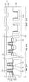
도 1a 내지 도 1d는 본 발명의 일 실시예에 따른 폴리 오픈 평탄화 방법을 나타내는 단면도들이다.
도 2a 내지 도 2l은 본 발명의 일 실시예에 따른 트랜지스터 제조 방법을 나타내는 단면도들이다.
도 3은 본 발명의 실시예들에 따른 메모리 시스템을 설명하기 위한 블록도이다.
도 4는 본 발명의 실시예들에 따른 메모리 시스템을 설명하기 위한 블록도이다.1A through 1D are cross-sectional views illustrating a poly-open planarization method according to an embodiment of the present invention.
2A to 2L are cross-sectional views illustrating a method of manufacturing a transistor according to an embodiment of the present invention.
3 is a block diagram illustrating a memory system according to embodiments of the present invention.
4 is a block diagram illustrating a memory system according to embodiments of the present invention.
이하, 첨부한 도면을 참조하여 본 발명의 바람직한 실시예를 상세히 설명하고자 한다.Hereinafter, preferred embodiments of the present invention will be described in detail with reference to the accompanying drawings.
본 발명의 각 도면에 있어서, 구조물들의 치수는 본 발명의 명확성을 기하기 위하여 실제보다 확대하여 도시한 것이다.In the drawings of the present invention, the dimensions of the structures are enlarged to illustrate the present invention in order to clarify the present invention.
본 발명에서, 제1, 제2 등의 용어는 다양한 구성요소들을 설명하는데 사용될 수 있지만, 상기 구성요소들은 상기 용어들에 의해 한정되어서는 안 된다. 상기 용어들은 하나의 구성요소를 다른 구성요소로부터 구별하는 목적으로만 사용된다.In the present invention, the terms first, second, etc. may be used to describe various elements, but the elements should not be limited by the terms. The terms are used only for the purpose of distinguishing one component from another.
본 발명에서 사용한 용어는 단지 특정한 실시예를 설명하기 위해 사용된 것으로, 본 발명을 한정하려는 의도가 아니다. 단수의 표현은 문맥상 명백하게 다르게 뜻하지 않는 한, 복수의 표현을 포함한다. 본 출원에서, "포함하다" 또는 "가지다" 등의 용어는 명세서 상에 기재된 특징, 숫자, 단계, 동작, 구성요소, 부품 또는 이들을 조합한 것이 존재함을 지정하려는 것이지, 하나 또는 그 이상의 다른 특징들이나 숫자, 단계, 동작, 구성요소, 부품 또는 이들을 조합한 것들의 존재 또는 부가 가능성을 미리 배제하지 않는 것으로 이해되어야 한다.The terminology used herein is for the purpose of describing particular embodiments only and is not intended to be limiting of the invention. The singular expressions include plural expressions unless the context clearly dictates otherwise. In the present application, the terms "comprises" or "having" and the like are used to specify that there is a feature, a number, a step, an operation, an element, a component or a combination thereof described in the specification, But do not preclude the presence or addition of one or more other features, integers, steps, operations, elements, components, or combinations thereof.
본 발명에 있어서, 각 층(막), 영역, 전극, 패턴 또는 구조물들이 대상체, 기판, 각 층(막), 영역, 전극 또는 패턴들의 "상에", "상부에" 또는 "하부"에 형성되는 것으로 언급되는 경우에는 각 층(막), 영역, 전극, 패턴 또는 구조물들이 직접 기판, 각 층(막), 영역, 또는 패턴들 위에 형성되거나 아래에 위치하는 것을 의미하거나, 다른 층(막), 다른 영역, 다른 전극, 다른 패턴 또는 다른 구조물들이 대상체나 기판 상에 추가적으로 형성될 수 있다.In the present invention, it is to be understood that each layer (film), region, electrode, pattern or structure may be formed on, over, or under the object, substrate, layer, Means that each layer (film), region, electrode, pattern or structure is directly formed or positioned below a substrate, each layer (film), region, or pattern, , Other regions, other electrodes, other patterns, or other structures may additionally be formed on the object or substrate.
본문에 개시되어 있는 본 발명의 실시예들에 대해서, 특정한 구조적 내지 기능적 설명들은 단지 본 발명의 실시예를 설명하기 위한 목적으로 예시된 것으로, 본 발명의 실시예들은 다양한 형태로 실시될 수 있으며 본문에 설명된 실시예들에 한정되는 것으로 해석되어서는 안된다.For the embodiments of the invention disclosed herein, specific structural and functional descriptions are set forth for the purpose of describing an embodiment of the invention only, and it is to be understood that the embodiments of the invention may be practiced in various forms, But should not be construed as limited to the embodiments set forth in the claims.
즉, 본 발명은 다양한 변경을 가할 수 있고 여러 가지 형태를 가질 수 있는 바, 특정 실시예들을 도면에 예시하고 본문에 상세하게 설명하고자 한다. 그러나, 이는 본 발명을 특정한 개시 형태에 대해 한정하려는 것이 아니며, 본 발명의 사상 및 기술 범위에 포함되는 모든 변경, 균등물 내지 대체물을 포함하는 것으로 이해되어야 한다.
That is, the present invention is capable of various modifications and various forms, and specific embodiments are illustrated in the drawings and described in detail in the following description. It should be understood, however, that the invention is not intended to be limited to the particular forms disclosed, but includes all modifications, equivalents, and alternatives falling within the spirit and scope of the invention.
도 1a 내지 도 1d는 본 발명의 일 실시예에 따른 폴리 오픈 평탄화 방법을 나타내는 단면도들이다.1A through 1D are cross-sectional views illustrating a poly-open planarization method according to an embodiment of the present invention.
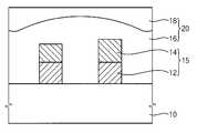
도 1a를 참조하면, 기판(10) 상에 폴리실리콘막(도시안함) 및 하드 마스크막(도시안함)을 형성한다. 상기 하드 마스크막은 실리콘 질화물로 이루어질 수 있다.Referring to FIG. 1A, a polysilicon film (not shown) and a hard mask film (not shown) are formed on a
상기 하드 마스크막을 패터닝하여 하드 마스크 패턴들(14)을 형성한다. 또한, 상기 하드 마스크 패턴들(14)을 식각 마스크로 사용하여 상기 폴리실리콘막을 식각함으로써, 폴리실리콘막 패턴들(12)을 형성한다. 상기 공정을 수행함으로써, 상기 기판(10) 상에는 폴리실리콘 패턴(12) 및 하드 마스크 패턴(14)이 적층된 적층 구조물들(15)이 형성된다.The hard mask film is patterned to form
그런데, 상기 하드 마스크막은 증착 상태에서의 두께 산포가 있다. 또한, 상기 폴리실리콘막을 식각하는 공정을 수행할 때 상기 하드 마스크 패턴들(14)도 데미지를 입기 때문에 상기 적층 구조물들(15)에 포함된 하드 마스크 패턴들(14)은 두께 산포가 생기게 된다. 즉, 상기 기판(10) 내에서 상기 하드 마스크 패턴들(14)은 균일한 두께를 갖지 못하게 된다. 또한, 상기 공정을 동일하게 수행한 각 기판들별로도 상기 하드 마스크 패턴들(14)의 두께 산포가 크게 발생하게 된다.Incidentally, the hard mask film has a thickness scattering in a deposition state. Also, since the
상기 적층 구조물들(15)을 덮는 제1 예비 층간 절연막(20)을 형성한다. 상기 제1 예비 층간 절연막(20)의 상부면은 상기 적층 구조물(15)의 상부면보다 높게 위치하도록 형성할 수 있다. 상기 제1 예비 층간 절연막(20)은 실리콘 산화물로 이루어질 수 있다.A first preliminary
후속의 연마 공정을 용이하게 수행하도록 하기 위하여, 상기 제1 예비 층간 절연막(20)은 상부면이 평탄한 상태로 증착되는 것이 바람직하다. 이를 위하여, 상기 제1 예비 층간 절연막(20)은 다층의 절연막으로 형성할 수 있다. 일 예로, 상기 제1 예비 층간 절연막(20)은 갭필 능력이 우수한 특성을 갖는 제1 절연 물질막(16)을 먼저 형성하고, 증착 두께 산포가 작은 제2 절연 물질막(18)을 적층시켜 형성할 수 있다. 이와같이, 두께 산포가 작은 제2 절연 물질막(18)을 상부에 증착함으로써, 기판(10) 내의 각 영역별로 제1 예비 층간 절연막(20)의 두께 산포를 감소시킬 수 있다. 구체적으로, 상기 제1 절연 물질막(16)은 고밀도 플라즈마 산화막으로 형성할 수 있고, 상기 제2 절연 물질막(18)은 TEOS막으로 형성할 수 있다. 후속 공정을 통해 연마가 완료되었을 때, 상기 폴리실리콘 패턴 양측으로 제1 절연 물질막만(16)이 남도록 하는 것이 바람직하다. 그러므로, 상기 제1 절연 물질막(16)은 그 상부면이 적어도 상기 폴리실리콘 패턴 상부면보다 높게 위치되도록 형성할 수 있다.In order to facilitate the subsequent polishing process, it is preferable that the first preliminary
도 1b를 참조하면, 상기 하드 마스크 패턴들(14) 중 적어도 일부의 하드 마스크 패턴들(14)의 상부면이 노출되도록 상기 제1 예비 층간 절연막(20)을 1차 연마하여 제2 예비 층간 절연막(22)을 형성한다. 즉, 상기 하드 마스크 패턴들(14) 중에 두께가 두꺼운 하드 마스크 패턴들(14)은 상부면이 노출되도록 한다. 그러나, 상기 하드 마스크 패턴들(14) 중에서 상대적으로 얇은 두께를 갖는 하드 마스크 패턴들(14) 상에는 제2 예비 층간 절연막(22)이 남아있도록 함으로써, 상기 하드 마스크 패턴(14)의 상부면이 노출되지 않도록 한다.Referring to FIG. 1B, the first preliminary
상기 1차 연마 공정을 통해 형성되는 제2 예비 층간 절연막(22)은 상부면이 높은 평탄도를 갖는 것이 바람직하다. 즉, 상기 기판(10) 내에서, 상기 기판(10) 표면으로부터 상기 제2 예비 층간 절연막(22) 상부면까지의 두께의 산포는 상기 하드 마스크 패턴(14)의 두께 산포보다 작게되도록 하여야 한다. 여기서, 두께 산포는 기판 위치별로 동일한 박막의 최대 두께 차이를 의미한다. 또한, 상기 기판(10) 내에서, 상기 기판(10) 표면으로부터 상기 제2 예비 층간 절연막(22) 상부면까지의 두께의 산포는 200Å보다 작은 것이 바람직하다.The upper surface of the second preliminary
일 예로, 상기 1차 연마 공정은 2가지 슬러리를 이용하여 수행할 수 있다. 먼저, 상기 제1 예비 층간 절연막(20)을 빠르게 제거하는 제1 슬러리를 사용하여, 상기 하드 마스크 패턴들(14)이 노출되지 않도록 상기 제1 예비 층간 절연막(16)을 일부 두께만큼 연마한다. 이 때, 상기 제1 슬러리는 실리콘 산화물과 실리콘 질화물 간의 연마 선택비를 갖지 않아도 된다. 상기 제1 슬러리는 건식 실리카(Fumed silica) 슬러리를 사용할 수 있다. 계속하여, 상기 하드 마스크 패턴들(14) 상부면이 노출되었을 때 연마 속도가 느려지는 제2 슬러리를 사용하여, 적어도 일부의 하드 마스크 패턴들(14)의 상부면이 노출되도록 상기 제1 예비 층간 절연막(20)을 연마한다. 즉, 일부의 하드 마스크 패턴(14)의 상부면이 노출되면, 더 이상 제1 예비 층간 절연막(20) 및 하드 마스크 패턴(14)의 연마 속도가 느려지도록 한다. 상기 제2 슬러리는 자동 정지 세리아(Auto Stop Ceria) 슬러리를 사용할 수 있다. 이로써, 상기 연마 공정을 통해 형성되는 제2 예비 층간 절연막(22)은 높은 평탄도를 갖게된다.For example, the primary polishing process may be performed using two slurries. First, the first preliminary
다른 예로, 상기 1차 연마 공정은 상기 하드 마스크 패턴(14) 상부면이 노출되었을 때 연마 속도가 느려지는 상기 제2 슬러리만을 사용하여 수행할 수도 있다.As another example, the primary polishing process may be performed using only the second slurry where the polishing rate is slowed when the upper surface of the
도 1c를 참조하면, 상기 하드 마스크 패턴들(14) 상부면이 모두 노출되도록 상기 제2 예비 층간 절연막(22)을 건식 식각 공정을 통해 일부 두께만큼 제거하여 제3 예비 층간 절연막(24)을 형성한다. 상기 제2 예비 층간 절연막(22)의 식각은 상기 하드 마스크 패턴(14)과의 식각 선택비가 높은 조건의 건식 식각 공정으로 수행될 수 있다. 즉, 상기 식각 공정을 통해 상기 하드 마스크 패턴(14)은 거의 식각되지 않는 것이 바람직하다.Referring to FIG. 1C, the second preliminary
상기 건식 식각 공정을 통해 제2 예비 층간 절연막(22)을 일부 두께만큼 제거함으로써, 후속의 2차 연마 공정 시에 상기 제3 예비 층간 절연막(24)이 제거되는 두께를 감소시킬 수 있다. 그러므로, 2차 연마 공정 시에 하드 마스크 패턴(14)과 제3 예비 층간 절연막(24)간의 연마 속도의 차이에 의해 발생되는 디싱 불량 등을 감소시킬 수 있다.By removing the second preliminary
상기 제3 예비 층간 절연막(24)의 상부면은 상기 하드 마스크 패턴들(14)의 상부면보다 낮게 위치하도록 하는 것이 바람직하다. 또한, 상기 제3 예비 층간 절연막(24)의 상부면은 상기 폴리실리콘 패턴(12)의 상부면보다 높게 위치하도록 하는 것이 바람직하다.The upper surface of the third
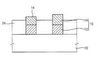
도 1d를 참조하면, 상기 폴리실리콘 패턴들(12)이 노출되도록 상기 하드 마스크 패턴(14) 및 제3 예비 층간 절연막(24)을 2차 연마하여 층간 절연막(26)을 형성한다. 상기 층간 절연막(26) 및 폴리실리콘 패턴(12)의 상부면은 평탄하게 되는 것이 바람직하다. 또한, 상기 연마 공정에 의해 상기 하드 마스크 패턴들(14)은 모두 제거된다.Referring to FIG. 1D, the
상기 제2 연마 공정은 상기 하드 마스크 패턴들(14) 및 제3 예비 층간 절연막(24)의 연마 속도보다 상기 폴리실리콘 패턴(12)의 연마 속도가 느린 제3 슬러리를 사용하여 수행할 수 있다. 일 예로, 상기 제3 슬러리는 콜로이들 실리카(colloidal silica)를 사용할 수 있다.The second polishing process may be performed using a third slurry having a polishing rate lower than the polishing rate of the
상기 제2 연마 공정을 수행할 때, 상기 하드 마스크 패턴(14)은 상기 제3 예비 층간 절연막(24)보다 빠르게 연마될 수 있다. 또한, 상기 폴리실리콘 패턴(12)은 거의 연마되지 않는다. 그런데, 상기 제3 예비 층간 절연막(24)의 상부면은 상기 하드 마스크 패턴(14)의 상부면보다 낮게 위치한다. 때문에, 상기 하드 마스크 패턴(14)이 제거되도록 연마 공정을 수행하면 남아있는 폴리실리콘 패턴(12) 및 층간 절연막(26)의 상부면이 매우 평탄해진다. 또한, 상기 폴리실리콘 패턴(12)과 층간 절연막(26)의 상부면이 평탄해지기 위하여, 연마하여야 할 상기 제3 예비 층간 절연막(24)의 두께가 감소된다. 그러므로, 상기 연마 공정 시간을 단축할 수 있으며 이로 인해 주변 영역에 형성되어있는 단차를 갖는 각 패턴들이 상기 연마 공정에 의해 손상되는 것을 최소화할 수 있다.When the second polishing process is performed, the
상기 설명한 공정을 통해, 층간 절연막(26)과 폴리실리콘 패턴(12)간의 평탄도가 높게 되도록 하면서 상기 폴리실리콘 패턴(12)의 상부면을 노출시킬 수 있다. 상기 평탄화 공정을 이용하여 다양한 반도체 소자를 제조할 수 있다.
The upper surface of the
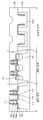
도 2a 내지 도 2l은 본 발명의 일 실시예에 따른 트랜지스터 제조 방법을 나타내는 단면도들이다.2A to 2L are cross-sectional views illustrating a method of manufacturing a transistor according to an embodiment of the present invention.
도 2a를 참조하면, 단결정 실리콘으로 이루어지는 기판(100)을 마련한다. 상기 기판(100)에는 NMOS 트랜지스터, PMOS 트랜지스터, 포토키 등이 형성되어야 하므로, PMOS 형성 영역, NMOS 형성 영역 및 포토키 형성 영역 등으로 구분될 수 있다.Referring to FIG. 2A, a
상기 기판(100)에 소자 분리 공정을 수행하여 소자 분리막 패턴(102)을 형성한다. 또한, 상기 포토키 형성 영역의 기판(100)을 식각하여 단차부를 갖는 포토키 패턴(100a)을 형성한다. 상기 포토키 패턴(100a)의 단차부 표면에는 절연막(102a)이 증착될 수 있다.A device isolation process is performed on the
상기 기판(100) 상에 게이트 절연막(104)을 형성한다. 상기 게이트 절연막(104)은 실리콘 질화물보다 높은 유전율을 갖는 금속 산화물을 증착하여 형성할 수 있다. 상기 금속 산화물로 사용될 수 있는 물질의 예로는 Ta2O5, Ta2O5N, Al2O5, HfO2, ZrO2, TiO2 등을 들 수 있다. 상기 물질들은 단독으로 사용되는 것이 바람직하지만, 2 이상이 사용될 수도 있다.A
상기 게이트 절연막(104) 상에, 상기 게이트 절연막(104)을 보호하기 위한 보호막(106)을 형성할 수 있다. 상기 보호막(106)은 후속 공정을 수행할 때 게이트 절연막에 어택을 입지 않도록 하는 역할을 하며, 도전성 물질로 이루어질 수 있다. 상기 보호막(106)으로 사용될 수 있는 물질의 예로는 티타늄, 티타늄 질화물, 탄탈륨, 탄탈륨 질화물 등을 들 수 있다. 이들 물질은 단독으로 사용되거나 또는 2 이상이 사용될 수 있다. 상기 보호막(106)은 수 내지 수십 Å의 얇은 두께를 갖도록 형성한다.A
도 2b를 참조하면, 상기 보호막(106) 상에 폴리실리콘막(도시안함) 및 하드 마스크막(도시안함)을 형성한다. 상기 하드 마스크막은 실리콘 질화물로 이루어질 수 있다.Referring to FIG. 2B, a polysilicon film (not shown) and a hard mask film (not shown) are formed on the
상기 하드 마스크막을 패터닝하여 하드 마스크 패턴들(110)을 형성한다. 또한, 상기 하드 마스크 패턴들(110)을 식각 마스크로 사용하여 상기 폴리실리콘막을 식각함으로써, 폴리실리콘막 패턴들(108)을 형성한다. 상기 폴리실리콘막 패턴(108)은 후속 공정을 통해 제거되어 금속 게이트 전극이 형성될 부분이 된다. 그러므로, 상기 폴리실리콘막 패턴(108)은 NMOS 및 PMOS 트랜지스터의 게이트 전극이 형성되어야 할 위치에 형성된다.The hard mask film is patterned to form
계속하여, 상기 하드 마스크 패턴(110)을 식각 마스크로 이용하여 상기 보호막(106) 및 게이트 절연막(104)을 식각할 수 있다. 이로써, 보호막 패턴(106a) 및 게이트 절연막 패턴(104a)을 형성한다.Subsequently, the
상기 공정을 수행함으로써, 상기 기판(100) 상에는 게이트 절연막 패턴(104a), 보호막 패턴(106a), 폴리실리콘 패턴(108) 및 하드 마스크 패턴(110)이 적층된 적층 구조물들(111)이 형성된다.By performing the above process, stacked
도 2c를 참조하면, 상기 적층 구조물(111)의 표면 및 기판(100) 표면을 따라 제1 스페이서막(도시안함)을 형성한다. 상기 제1 스페이서막은 층간 절연막으로 제공되는 박막과 식각 선택비를 갖는 물질로 형성할 수 있다. 일 예로, 상기 제1 스페이서막은 실리콘 질화물을 증착시켜 형성할 수 있다. 상기 제1 스페이서막을 이방성 식각함으로써, 상기 적층 구조물(111)의 양 측벽에 제1 스페이서(112)를 형성한다.Referring to FIG. 2C, a first spacer film (not shown) is formed along the surface of the stacked
상기 적층 구조물(111) 양 측의 기판(100)에 불순물 영역을 형성한다. 즉, NMOS 영역의 기판에 선택적으로 N형 불순물을 주입시킨다. 따라서, NMOS 트랜지스터의 소오스 및 드레인 영역(116)을 형성한다. 또한, PMOS 영역의 기판에 선택적으로 P형 불순물을 주입시킨다. 이로써, PMOS 트랜지스터의 소오스 및 드레인 영역(118)을 형성한다.An impurity region is formed on the
계속하여, 상기 제1 스페이서(112), 적층 구조물(111) 상부면 및 기판(100) 상에 제2 스페이서막(도시안함)을 형성한다. 상기 제2 스페이서막은 제1 스페이서막과 다른 절연 물질로 형성할 수 있다. 일 예로, 상기 제2 스페이서막은 실리콘 산화물로 형성할 수 있다. 상기 제2 스페이서막을 이방성 식각하여 제2 스페이서(114)를 형성한다. 상기 제2 스페이서(114)는 후속 공정에서 실리콘 게르마늄 패턴이 형성될 부위를 한정하는 역할을 한다. 즉, 후속 공정에서, 상기 제2 스페이서(114) 사이에 노출되는 기판(100) 부위에 상기 실리콘 게르마늄 패턴이 형성된다.Subsequently, a second spacer film (not shown) is formed on the
도 2d를 참조하면, 상기 PMOS 트랜지스터 영역의 기판(100)이 선택적으로 노출되도록 상기 기판(100) 상에 마스크 패턴(119)을 형성한다. 상기 마스크 패턴(119)은 NMOS 트랜지스터 영역의 기판(100) 및 포토키 영역의 기판(100)을 덮는다.Referring to FIG. 2D, a
이 후, 상기 PMOS 트랜지스터 영역의 노출된 기판(100) 부위에 선택적으로 실리콘 게르마늄을 성장시켜 실리콘 게르마늄 패턴(120)을 형성한다. 상기 실리콘 게르마늄 패턴(120)을 형성하면, 상기 PMOS 트랜지스터의 채널 영역의 격자 간격이 변화된다. 이로인해, 상기 PMOS 트랜지스터의 홀의 이동도가 향상된다. 상기 실리콘 게르마늄 패턴(120)을 형성하고 난 다음, 상기 마스크 패턴(119)을 제거한다.Thereafter, silicon germanium is selectively grown on the exposed portion of the
도 2e를 참조하면, 상기 기판(100), 하드 마스크 패턴(110) 및 제2 스페이서(114)의 표면을 따라 금속 실리사이드 형성을 위한 금속막(도시안함)을 형성한다. 상기 금속막으로 사용할 수 있는 금속 물질의 예로는 니켈, 플레티늄 등을 들 수 있다. 이들은 단독으로 사용하거나 또는 복합적으로 사용할 수 있다.Referring to FIG. 2E, a metal film (not shown) for forming a metal silicide is formed along the surfaces of the
이 후, 상기 금속막과 상기 기판(100)을 반응시켜 상기 기판(100) 표면 상에 금속 실리사이드 패턴(122)을 형성한다. 상기 금속 실리사이드 패턴(122)은 니켈 실리사이드, 플레티늄 실리사이드 또는 니켈 플레티늄 실리사이드일 수 있다. 이 후, 미반응한 상기 금속막을 제거한다. 상기 금속 실리사이드 패턴(122)은 소오스/드레인들과 후속 공정을 통해 형성되는 콘택 플러그 간의 저항을 감소시키는 역할을 한다.Thereafter, the metal film and the
이 후, 상기 금속 실리사이드 패턴(122), 하드 마스크 패턴(110) 및 제2 스페이서(114)의 표면을 따라 식각 저지막(도시안함)을 형성할 수 있다. 상기 식각 저지막은 상기 소오스/드레인들과 접촉하는 콘택 플러그들을 형성하는 공정에서 정확하게 식각이 종료될 수 있도록 하기 위하여 제공된다.Thereafter, an etch stop layer (not shown) may be formed along the surfaces of the
상기 설명한 것과 같이, 폴리실리콘 패턴(108) 및 하드 마스크 패턴(110)을 형성한 다음에, 제1 및 제2 스페이서(112, 114) 형성, 실리콘 게르마늄 패턴(120) 성장 및 금속 실리사이드 패턴(122) 형성 등과 같은 공정들이 수행된다. 때문에, 상기 공정들을 수행할 때, 각각의 하드 마스크 패턴들(110)은 어택을 받게되어 일부 제거될 수 있다. 또한, 각각의 하드 마스크 패턴들(110)은 위치별로 서로 동일하지 않은 어택을 받을 수 있다. 예를들어, 상기 실리콘 게르마늄 패턴(120)을 형성하기 전 마스크 패턴(119)을 형성하는 공정에서, 상기 PMOS 영역에 형성된 하드 마스크 패턴(110)만이 노출되어 있으므로 상대적으로 상기 PMOS 영역에 형성된 하드 마스크 패턴(110)이 더 많은 어택을 받게된다. 그러므로, 상기 공정들이 완료된 다음에, 상기 적층 구조물(111)에 포함된 하드 마스크 패턴들(110)은 두께 산포가 생기게 된다. 즉, 상기 기판(100) 내에서 상기 하드 마스크 패턴들(110)은 균일한 두께를 갖지 못하게 된다. 또한, 상기 각 공정을 동일하게 수행한 서로 다른 기판별로도 상기 하드 마스크 패턴(110)의 두께 산포가 크게 발생하게 된다. 일 예로, 상기 기판(100) 내에서 상기 하드 마스크 패턴들(110)은 300 내지 500Å정도의 두께 산포를 갖게된다. 이와같이, 상기 하드 마스크 패턴들(110)의 두께 산포가 클 경우, 통상적인 연마 공정을 수행하였을 때 원하는 수준의 높은 평탄도를 가질 수 없게 된다. 그리고, 상기 두께 산포가 클 경우에는 연마 정지 포인트를 설정하기가 어려우므로, 과도 연마가 되거나 연마가 일부 되지 않는 등의 불량이 발생될 수 있다.After forming the
도 2f를 참조하면, 상기 적층 구조물(111)을 덮는 제1 예비 층간 절연막(127)을 형성한다. 상기 제1 예비 층간 절연막(127)의 상부면은 상기 적층 구조물(111)의 상부면보다 높게 위치하여야 한다. 상기 제1 예비 층간 절연막(127)은 실리콘 산화물로 이루어질 수 있다.Referring to FIG. 2F, a first preliminary
후속의 연마 공정을 용이하게 수행하여 상기 제1 예비 층간 절연막(127)의 상부면이 평탄한 상태로 증착되는 것이 바람직하다. 이를 위하여, 상기 제1 예비 층간 절연막(127)은 2층 이상의 막으로 형성될 수 있다. 일 예로, 갭필 능력이 우수한 특성을 갖는 제1 절연 물질막(124)을 먼저 형성하고, 증착 두께 산포가 작은 제2 절연 물질막(126)을 적층시켜 형성할 수 있다. 이와같이, 두께 산포가 작은 제2 절연 물질막(126)을 상부에 증착함으로써, 기판 내의 각 영역별로 제1 예비 층간 절연막(127)의 두께 산포를 감소시킬 수 있다. 구체적으로, 상기 제1 절연 물질막(124)은 고밀도 플라즈마 산화막으로 형성할 수 있고, 상기 제2 절연 물질막(126)은 TEOS막으로 형성할 수 있다.It is preferable that the upper surface of the first preliminary
상기 제1 절연 물질막(124)은 상기 적층 구조물 사이를 채우도록 형성할 수 있다. 또한, 상기 제1 절연 물질막(124)의 상부면은 적어도 상기 폴리실리콘 패턴의 상부면보다 높게 위치하도록 형성할 수 있다. 이 경우, 후속의 평탄화 공정이 완료되면, 상기 제2 절연 물질막(126)은 모두 제거되고 상기 폴리실리콘 패턴(108)의 양측으로 제1 절연 물질막(124)만이 남게된다.The first insulating
도 2g를 참조하면, 상기 하드 마스크 패턴들(110) 중 적어도 일부의 하드 마스크 패턴들(110)의 상부면이 노출되도록 상기 제1 예비 층간 절연막(127)을 1차 연마하여 제2 예비 층간 절연막(128)을 형성한다. 즉, 상기 하드 마스크 패턴들(110) 중에 두께가 두꺼운 하드 마스크 패턴들(110)은 상부면이 노출되도록 한다. 그러나, 상기 하드 마스크 패턴들(110) 중에서 상대적으로 얇은 두께를 갖는 하드 마스크 패턴들(110) 상에는 제2 예비 층간 절연막(128)이 남아있도록 함으로써, 상기 하드 마스크 패턴(110)의 상부면이 노출되지 않도록 한다.Referring to FIG. 2G, the first preliminary
상기 1차 연마 공정을 통해 형성되는 제2 예비 층간 절연막(128)은 상부면이 높은 평탄도를 가져야 한다. 즉, 상기 기판(100) 내에서, 상기 기판(100) 표면으로부터 상기 제2 예비 층간 절연막(128) 상부면까지의 두께의 산포는 상기 하드 마스크 패턴(110)의 두께 산포보다 작게되도록 하여야 한다. 또한, 상기 기판(100) 내에서, 상기 기판(100) 표면으로부터 상기 제2 예비 층간 절연막(128) 상부면까지의 두께의 산포는 200Å보다 작은 것이 바람직하다. 즉, 상기 폴리실리콘 패턴(108) 상부면에 남아있는 상기 제2 예비 층간 절연막(128)은 0 내지 200Å인 것이 바람직하다.The upper surface of the second preliminary
일 예로, 상기 1차 연마 공정은 2가지 슬러리를 이용하여 수행할 수 있다. 먼저, 상기 제1 예비 층간 절연막(127)을 빠르게 제거하는 제1 슬러리를 사용하여, 상기 하드 마스크 패턴들(110)이 노출되지 않도록 상기 제1 예비 층간 절연막(127)을 일부 두께만큼 연마한다. 이 때, 상기 제1 슬러리는 실리콘 산화물과 실리콘 질화물 간의 연마 선택비를 갖지 않아도 된다. 상기 제1 슬러리는 실리카 슬러리일 수 있다. 계속하여, 상기 하드 마스크 패턴들(110) 상부면이 노출되었을 때 연마 속도가 느려지는 제2 슬러리를 사용하여, 적어도 일부의 하드 마스크 패턴들(110)의 상부면이 노출되도록 상기 제1 예비 층간 절연막(127)을 연마한다. 즉, 일부의 하드 마스크 패턴(110)의 상부면이 노출되면, 더 이상 제1 예비 층간 절연막(127) 및 하드 마스크 패턴(110)의 연마 속도가 느려지도록 한다. 이로써, 상기 연마 공정을 통해 형성되는 제2 예비 층간 절연막(128)은 높은 평탄도를 갖게된다. 상기 제2 슬러리는 자동 정지 세리아 슬러리일 수 있다.For example, the primary polishing process may be performed using two slurries. First, the first preliminary
다른 예로, 상기 1차 연마 공정은 상기 하드 마스크 패턴들(110) 상부면이 노출되었을 때 연마 속도가 느려지는 상기 제2 슬러리만을 사용하여 수행할 수도 있다.As another example, the primary polishing process may be performed using only the second slurry where the polishing rate is slowed when the upper surface of the
도 2h를 참조하면, 적어도 상기 하드 마스크 패턴(110)들 상부면이 모두 노출되도록 상기 제2 예비 층간 절연막(128)을 건식 식각 공정을 통해 일부 두께만큼 제거하여 제3 예비 층간 절연막(130)을 형성한다. 상기 건식 식각은 상기 하드 마스크 패턴(110)과의 식각 선택비가 높은 조건으로 수행된다. 즉, 상기 건식 식각 공정을 수행할 때 상기 하드 마스크 패턴(110)은 거의 식각되지 않도록 한다.Referring to FIG. 2H, the second preliminary
상기 제3 예비 층간 절연막(130)의 상부면은 상기 하드 마스크 패턴(110)의 상부면보다 낮게 위치하도록 하는 것이 바람직하다. 또한, 상기 제3 예비 층간 절연막(130)의 상부면은 상기 폴리실리콘 패턴(108)의 상부면보다 높게 위치하도록 하는 것이 바람직하다.The upper surface of the third
상기 건식 식각 공정을 통해 제2 예비 층간 절연막(128)을 일부 두께만큼 제거함으로써, 후속의 2차 연마 공정 시에 상기 제3 예비 층간 절연막(130)의 제거 두께를 감소시킬 수 있다. 그러므로, 2차 연마 공정 시에 하드 마스크 패턴(110)과 제3 예비 층간 절연막(130)간의 연마 속도의 차이에 의해 발생되는 디싱 불량 등을 감소시킬 수 있다.By removing the second preliminary
도 2i를 참조하면, 상기 폴리실리콘 패턴들(108)이 노출되도록 상기 하드 마스크 패턴(110) 및 제3 예비 층간 절연막(130)을 2차 연마하여 층간 절연막(132)을 형성한다. 상기 층간 절연막(132) 및 폴리실리콘 패턴(108)의 상부면은 평탄한 것이 바람직하다.Referring to FIG. 2I, the
상기 제2 연마 공정은 상기 하드 마스크 패턴들(110) 및 제3 예비 층간 절연막(130)의 연마 속도보다 상기 폴리실리콘 패턴(108)의 연마 속도가 느린 제3 슬러리를 사용하여 수행할 수 있다. 일 예로, 상기 제3 슬러리는 콜로이들 실리카(colloidal silica)를 사용할 수 있다.The second polishing process may be performed using a third slurry in which the polishing rate of the
상기 제2 연마 공정을 수행할 때, 상기 하드 마스크 패턴(110)은 상기 제3 예비 층간 절연막(130)보다 빠르게 연마될 수 있다. 그런데, 상기 제3 예비 층간 절연막(130)의 상부면은 상기 하드 마스크 패턴(110)의 상부면보다 낮게 위치한다. 때문에, 상기 하드 마스크 패턴(110)이 제거되도록 연마 공정을 수행하면 남아있는 폴리실리콘 패턴(108) 및 층간 절연막(132)의 상부면이 매우 평탄해진다.When the second polishing process is performed, the
또한, 상기 폴리실리콘 패턴(108)과 층간 절연막(132)의 상부면이 평탄해지기 위하여, 연마하여야 할 상기 제3 예비 층간 절연막(130)의 두께가 감소된다. 그러므로, 상기 연마 공정 시간을 단축할 수 있으며 이로인해 주변 영역에 형성되어있는 단차를 갖는 각 패턴들이 상기 연마 공정에 의해 손상되는 것을 최소화할 수 있다. 구체적으로, 상기 연마 공정 시간이 단축됨으로써, 상기 포토키 패턴이 연마에 의해 붕괴되거나 단차가 낮아지는 불량을 감소시킬 수 있다. 더구나, 상기 연마 공정 시간이 단축됨으로써, 상기 하드 마스크 패턴과 동일한 물질로 이루어지는 식각 저지막(도시안됨) 부위가 과도하게 제거되지 않는다. 그러므로, 상기 식각 저지막 부위가 일부 제거되어 덴트(dent)가 생성되는 것을 억제할 수 있다.In addition, the thickness of the third preliminary
또한, 상기 연마 공정이 과도하게 수행되는 것을 억제할 수 있어, 과도 연마에 의해 상기 실리콘 게르마늄 패턴(120) 또는 금속 실리사이드 패턴(122)이 노출되는 등의 불량이 거의 발생되지 않는다.In addition, it is possible to suppress the polishing process from being excessively performed, and the defects such as the exposure of the
도 2j를 참조하면, 상기 노출된 폴리실리콘 패턴(108)을 선택적으로 제거하여 개구부(134)를 형성한다. 상기 폴리실리콘 패턴(108)을 선택적으로 제거하는 공정은 습식 식각 또는 건식 식각 공정을 통해 수행할 수 있다. 다른 예로, 상기 폴리실리콘 패턴(108) 상의 산화물을 제거하기 위한 건식 식각 공정을 먼저 수행한 후, 습식 식각 공정을 통해 상기 폴리실리콘 패턴(108)을 제거할 수 있다. 상기 개구부(134)의 저면에는 보호막이 노출되어 있다.Referring to FIG. 2J, the exposed
상기 개구부(134)가 형성된 층간 절연막들(132)은 매우 평탄한 상부면을 갖고 있으며, 두께 산포가 거의 없다. 때문에, 후속 공정을 수행함으로써, 상기 개구부(134) 내부에 균일한 두께를 갖는 게이트 전극을 용이하게 형성할 수 있다.The
도 2k를 참조하면, 상기 개구부(134) 내부를 채우도록 금속막(도시안함)을 형성한다. 상기 금속막은 NMOS 트랜지스터 및 PMOS 트랜지스터에 각각 적합한 일함수를 갖도록 조절하기에 용이한 금속 물질을 사용하여 형성할 수 있다. 일 예로, 상기 금속막은 알루미늄막으로 형성할 수 있다. 도시하지는 않았지만, 상기 금속막을 형성하기 이 전에 베리어 금속막(도시안함)을 먼저 형성할 수 있다. 상기 베리어 금속막으로 사용될 수 있는 물질의 예로는 티타늄, 티타늄 질화물, 탄탈륨, 탄탈륨 질화물 등을 들 수 있다.Referring to FIG. 2K, a metal film (not shown) is formed to fill the inside of the
상기 층간 절연막(132)의 상부면이 노출되도록 상기 금속막을 연마하여, 상기 개구부(134) 내부에 금속 물질로 이루어지는 게이트 전극(136)을 형성한다. 이로써, NMOS 트랜지스터 및 PMOS 트랜지스터가 완성된다. 설명한 것과 같이, 상기 트랜지스터를 제조하는 마지막 단계에서 금속을 포함하는 게이트 전극(136)이 형성된다.The metal film is polished so that the upper surface of the
도 2l을 참조하면, 상기 층간 절연막(132) 상에 상부 층간 절연막(140)을 형성한다. 상기 상부 층간 절연막(140)의 일부분을 식각하여 콘택홀들을 형성한다. 상기 콘택홀들은 NMOS 및 PMOS 트랜지스터의 소오스/드레인 및 게이트 전극(136)의 상부면을 노출하도록 형성할 수 있다. 상기 콘택홀들 내부에 도전 물질을 채워넣어 콘택 플러그들(142)을 형성한다.Referring to FIG. 21, an upper
본 실시예에 의하면, 상기 폴리실리콘 패턴을 노출하는 연마 공정에서 층간 절연막의 평탄도가 매우 높다. 또한, 상기 연마 공정을 수행한 이 후에, 덴트 불량 등이 거의 발생되지 않는다. 때문에, 게이트 전극을 공정의 마지막 단계에서 형성하는 게이트 라스트 공정을 수행하여, 기판 전 영역에서 균일한 두께를 가질 뿐 아니라 기판 간의 두께 편차도 매우 작은 게이트 전극을 형성할 수 있다. 그러므로, 특성 편차가 거의 없으면서 우수한 특성을 갖는 NMOS 및 PNOS 트랜지스터를 형성할 수 있다.
According to this embodiment, the flatness of the interlayer insulating film in the polishing step for exposing the polysilicon pattern is very high. Further, after the polishing step is performed, hardly any dent failure or the like occurs. Therefore, a gate electrode having a uniform thickness in the entire region of the substrate as well as a very small thickness variation between the substrates can be formed by performing the gate-last process of forming the gate electrode at the final stage of the process. Therefore, NMOS and PNOS transistors having excellent characteristics can be formed with little characteristic variation.
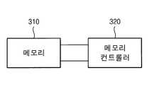
도 3은 본 발명의 실시예들에 따른 메모리 시스템을 설명하기 위한 블록도이다.3 is a block diagram illustrating a memory system according to embodiments of the present invention.
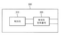
도 3을 참조하면, 본 실시예는 메모리 콘트롤러(320)와 연결된 메모리 소자(310)를 포함한다. 메모리 소자(310)는 각 실시예들에 따라 제조된 트랜지스터들이 포함될 수 있다. 메모리 콘트롤러(320)는 상기 메모리의 동작을 콘트롤하기 위한 입력 신호를 제공한다. 메모리 콘트롤러(320)는 인가 받은 콘트롤 신호를 기초로 메모리 소자(310)를 콘트롤할 수 있다.
Referring to FIG. 3, the present embodiment includes a
도 4는 본 발명의 실시예들에 따른 메모리 시스템을 설명하기 위한 블록도이다.4 is a block diagram illustrating a memory system according to embodiments of the present invention.
도 4를 참조하면, 본 실시예는 메모리(310)와 메모리 콘트롤러(320)가 메모리 카드(330) 내에 실장되는 것을 제외하고는 도 3과 동일하다. 예를 들어, 메모리 카드(330)는 각 실시예들에 따라 제조된 트랜지스터들이 포함되어 있는 메모리 카드일 수 있다. 일 예로, 상기 메모리 카드(330)에는 SRAM이 포함되어 있을 수도 있다. 즉, 메모리 카드(330)는 디지털 카메라, 퍼스널 컴퓨터 등과 같은 전자제품과 함께 사용되기 위한 산업적 표준에 맞는 카드일 수 있다. 메모리 콘트롤러(320)는 상기 다른 외부 장치로부터 카드에 의해 입력받은 콘트롤 신호에 기초하여 상기 메모리 소자(310)를 콘트롤할 수 있다.Referring to FIG. 4, the present embodiment is the same as FIG. 3 except that the
상기 설명한 것과 같이, 본 발명에 의하면 균일한 높이를 갖는 게이트 전극을 형성할 수 있다. 따라서, 상기 게이트 전극을 포함하는 고성능의 트랜지스터들을 형성할 수 있다. 또한, 상기 트랜지스터를 포함하는 다양한 반도체 메모리 소자 및 로직 소자들을 형성할 수 있다.As described above, according to the present invention, a gate electrode having a uniform height can be formed. Thus, high-performance transistors including the gate electrode can be formed. In addition, various semiconductor memory devices and logic devices including the transistors can be formed.
10 : 기판12 : 폴리실리콘 패턴
14 : 마스크 패턴15 : 적층 구조물
16 : 제1 절연 물질막18 : 제2 절연 물질막
20 : 제1 예비 층간 절연막22 : 제2 예비 층간 절연막
24 : 제3 예비 층간 절연막26 : 층간 절연막
100 : 기판102 : 소자 분리막 패턴
104 : 게이트 절연막106 : 보호막
108 : 폴리실리콘 패턴110 : 하드 마스크 패턴
111 : 적층 구조물112 : 제1 스페이서
114 : 제2 스페이서116, 118 : 소오스/드레인 영역
119 : 마스크 패턴120 : 실리콘 게르마늄 패턴
122 : 금속 실리사이드 패턴124 : 제1 절연 물질막
126 : 제2 절연 물질막127 : 제1 예비 층간 절연막
128 : 제2 예비 층간 절연막130 : 제3 예비 층간 절연막
132 : 층간 절연막134 : 개구부
136 : 게이트 전극140 : 상부 층간 절연막
142 : 콘택 플러그들10: substrate 12: polysilicon pattern
14: mask pattern 15: laminated structure
16: first insulating material film 18: second insulating material film
20: first preliminary interlayer insulating film 22: second preliminary interlayer insulating film
24: third preliminary interlayer insulating film 26: interlayer insulating film
100: substrate 102: element separation film pattern
104: gate insulating film 106: protective film
108: polysilicon pattern 110: hard mask pattern
111: laminated structure 112: first spacer
114:
119: mask pattern 120: silicon germanium pattern
122: metal silicide pattern 124: first insulating material film
126: second insulating material film 127: first preliminary interlayer insulating film
128: second preliminary interlayer insulating film 130: third preliminary interlayer insulating film
132: interlayer insulating film 134: opening
136: gate electrode 140: upper interlayer insulating film
142: contact plugs
Claims (10)
Translated fromKorean상기 하드 마스크 패턴들 상에 상기 하드 마스크 패턴들 상부면보다 높은 상부면을 갖는 제1 예비 층간 절연막을 형성하는 단계;
상기 하드 마스크 패턴들 중 적어도 일부의 하드 마스크 패턴들의 상부면이 노출되도록 상기 제1 예비 층간 절연막을 연마하는 1차 연마 공정을 수행하여 제2 예비 층간 절연막을 형성하는 단계;
상기 하드 마스크 패턴들의 상부면이 노출되도록 상기 제2 예비 층간 절연막을 식각하여 제3 예비 층간 절연막을 형성하는 단계;
상기 하드 마스크 패턴들 및 제3 예비 층간 절연막의 연마 속도보다 상기 폴리실리콘 패턴의 연마 속도가 느린 슬러리를 사용하여, 상기 폴리실리콘 패턴들이 노출되도록 상기 하드 마스크 패턴들 및 제3 예비 층간 절연막을 연마하는 2차 연마공정을 수행하여, 층간 절연막을 형성하는 단계;
상기 폴리실리콘 패턴을 제거하여 개구부를 형성하는 단계; 및
상기 개구부 내부에 금속 물질을 증착시켜 게이트 전극 패턴을 형성하는 단계를 포함하는 것을 특징으로 하는 반도체 소자 제조 방법.Forming stacked structures of a polysilicon pattern and a hard mask pattern on a substrate;
Forming a first preliminary interlayer insulating film having a top surface higher than the upper surface of the hard mask patterns on the hard mask patterns;
Forming a second preliminary interlayer insulating film by performing a first polishing step of polishing the first preliminary interlayer insulating film such that a top surface of at least some hard mask patterns of the hard mask patterns is exposed;
Forming a third preliminary interlayer insulating film by etching the second preliminary interlayer insulating film so that the upper surface of the hard mask patterns is exposed;
The hard mask patterns and the third preliminary interlayer insulating film are polished so that the polysilicon patterns are exposed using a slurry in which the polishing rate of the polysilicon pattern is slower than the polishing rate of the hard mask patterns and the third preliminary interlayer insulating film Performing a secondary polishing process to form an interlayer insulating film;
Removing the polysilicon pattern to form an opening; And
And forming a gate electrode pattern by depositing a metal material within the opening.
제1 슬러리를 사용하여, 상기 하드 마스크 패턴들이 노출되지 않도록 상기 제1 예비 층간 절연막을 일부 두께만큼 연마하는 단계; 및
상기 제1 슬러리와 다른 연마 특성을 갖는 제2 슬러리를 사용하여, 상기 제1 예비 층간 절연막을 연마하는 단계를 포함하는 것을 특징으로 하는 반도체 소자 제조 방법.The polishing method according to claim 1,
Using the first slurry, polishing the first preliminary interlayer insulating film to a certain thickness so that the hard mask patterns are not exposed; And
And polishing the first preliminary interlayer insulating film by using a second slurry having different polishing characteristics from the first slurry.
Priority Applications (2)
| Application Number | Priority Date | Filing Date | Title |
|---|---|---|---|
| KR1020100036331AKR101695902B1 (en) | 2010-04-20 | 2010-04-20 | Method of manufacturing a semiconductor device |
| US13/048,683US8470663B2 (en) | 2010-04-20 | 2011-03-15 | Methods of manufacturing a semiconductor device |
Applications Claiming Priority (1)
| Application Number | Priority Date | Filing Date | Title |
|---|---|---|---|
| KR1020100036331AKR101695902B1 (en) | 2010-04-20 | 2010-04-20 | Method of manufacturing a semiconductor device |
Publications (2)
| Publication Number | Publication Date |
|---|---|
| KR20110116735A KR20110116735A (en) | 2011-10-26 |
| KR101695902B1true KR101695902B1 (en) | 2017-01-13 |
Family
ID=44788498
Family Applications (1)
| Application Number | Title | Priority Date | Filing Date |
|---|---|---|---|
| KR1020100036331AActiveKR101695902B1 (en) | 2010-04-20 | 2010-04-20 | Method of manufacturing a semiconductor device |
Country Status (2)
| Country | Link |
|---|---|
| US (1) | US8470663B2 (en) |
| KR (1) | KR101695902B1 (en) |
Families Citing this family (3)
| Publication number | Priority date | Publication date | Assignee | Title |
|---|---|---|---|---|
| US9960050B2 (en)* | 2013-08-05 | 2018-05-01 | Taiwan Semiconductor Manufacturing Company Limited | Hard mask removal method |
| KR102230198B1 (en)* | 2014-09-23 | 2021-03-19 | 삼성전자주식회사 | Semiconductor device and method for manufacturing the same |
| KR102365108B1 (en)* | 2017-08-01 | 2022-02-18 | 삼성전자주식회사 | Integrated Circuit devices |
Family Cites Families (8)
| Publication number | Priority date | Publication date | Assignee | Title |
|---|---|---|---|---|
| JP4971559B2 (en) | 2001-07-27 | 2012-07-11 | ルネサスエレクトロニクス株式会社 | Manufacturing method of semiconductor device |
| KR100564580B1 (en)* | 2003-10-06 | 2006-03-29 | 삼성전자주식회사 | Oxide planarization method and manufacturing method of semiconductor device using same |
| KR100591719B1 (en)* | 2004-11-09 | 2006-06-22 | 삼성전자주식회사 | Method for manufacturing epitaxial contact plug, method for manufacturing semiconductor device using the method and method for manufacturing double stack transistor using the method |
| US7166506B2 (en) | 2004-12-17 | 2007-01-23 | Intel Corporation | Poly open polish process |
| JP4626411B2 (en)* | 2005-06-13 | 2011-02-09 | ソニー株式会社 | Semiconductor device and manufacturing method of semiconductor device |
| US7799630B2 (en) | 2008-01-23 | 2010-09-21 | United Microelectronics Corp. | Method for manufacturing a CMOS device having dual metal gate |
| KR20100006944A (en)* | 2008-07-11 | 2010-01-22 | 삼성전자주식회사 | Method of forming a isolation pattern and method of manufacturing a non-volatile memory device using the same |
| KR20100037212A (en)* | 2008-10-01 | 2010-04-09 | 주식회사 동부하이텍 | Semiconductor device and fabricating method thereof |
- 2010
- 2010-04-20KRKR1020100036331Apatent/KR101695902B1/enactiveActive
- 2011
- 2011-03-15USUS13/048,683patent/US8470663B2/enactiveActive
Also Published As
| Publication number | Publication date |
|---|---|
| US20110256676A1 (en) | 2011-10-20 |
| KR20110116735A (en) | 2011-10-26 |
| US8470663B2 (en) | 2013-06-25 |
Similar Documents
| Publication | Publication Date | Title |
|---|---|---|
| US20210391420A1 (en) | Fin recess last process for finfet fabrication | |
| US11864376B2 (en) | Semiconductor device including insulating element and method of making | |
| TWI689043B (en) | Transistor and methods of forming the same | |
| CN108122845B (en) | Contact structure manufacturing method and semiconductor device | |
| TWI700782B (en) | Semiconductor device and manufacturing method thereof | |
| US20150155208A1 (en) | Control Fin Heights in FinFET Structures | |
| TW201717398A (en) | Semiconductor device and method of manufacturing same | |
| CN107833891B (en) | Semiconductor device and method for manufacturing the same | |
| KR20180060911A (en) | Semiconductor device and manufacturing method thereof | |
| US20120292716A1 (en) | Dram structure with buried word lines and fabrication thereof, and ic structure and fabrication thereof | |
| KR20210053197A (en) | Semiconductor device and method | |
| US9564448B2 (en) | Flash memory structure | |
| US10636890B2 (en) | Chamfered replacement gate structures | |
| TWI767629B (en) | Semiconductor device and method for forming the same | |
| US20150255293A1 (en) | Planarization process | |
| US20170140984A1 (en) | Interconnect structure including middle of line (mol) metal layer local interconnect on etch stop layer | |
| KR101695902B1 (en) | Method of manufacturing a semiconductor device | |
| EP3240021B1 (en) | A method for fabricating a semiconductor structure | |
| TWI889014B (en) | Semiconductor device and method for manufacturing the same | |
| TWI802315B (en) | Method of forming semiconductor device | |
| KR101793160B1 (en) | Method of manufacturing a semiconductor device | |
| CN108807521B (en) | Semiconductor device and method for manufacturing the same | |
| US20160071867A1 (en) | Semiconductor device and method for fabricating the same | |
| US20240047458A1 (en) | Semiconductor device and method of forming the same | |
| US20250072048A1 (en) | Semiconductor device |
Legal Events
| Date | Code | Title | Description |
|---|---|---|---|
| PA0109 | Patent application | Patent event code:PA01091R01D Comment text:Patent Application Patent event date:20100420 | |
| PG1501 | Laying open of application | ||
| A201 | Request for examination | ||
| PA0201 | Request for examination | Patent event code:PA02012R01D Patent event date:20150403 Comment text:Request for Examination of Application Patent event code:PA02011R01I Patent event date:20100420 Comment text:Patent Application | |
| E902 | Notification of reason for refusal | ||
| PE0902 | Notice of grounds for rejection | Comment text:Notification of reason for refusal Patent event date:20160805 Patent event code:PE09021S01D | |
| E701 | Decision to grant or registration of patent right | ||
| PE0701 | Decision of registration | Patent event code:PE07011S01D Comment text:Decision to Grant Registration Patent event date:20170104 | |
| GRNT | Written decision to grant | ||
| PR0701 | Registration of establishment | Comment text:Registration of Establishment Patent event date:20170106 Patent event code:PR07011E01D | |
| PR1002 | Payment of registration fee | Payment date:20170109 End annual number:3 Start annual number:1 | |
| PG1601 | Publication of registration | ||
| FPAY | Annual fee payment | Payment date:20191226 Year of fee payment:4 | |
| PR1001 | Payment of annual fee | Payment date:20191226 Start annual number:4 End annual number:4 | |
| PR1001 | Payment of annual fee | Payment date:20201230 Start annual number:5 End annual number:5 | |
| PR1001 | Payment of annual fee | Payment date:20211229 Start annual number:6 End annual number:6 | |
| PR1001 | Payment of annual fee | Payment date:20221221 Start annual number:7 End annual number:7 | |
| PR1001 | Payment of annual fee | Payment date:20231226 Start annual number:8 End annual number:8 | |
| PR1001 | Payment of annual fee | Payment date:20241226 Start annual number:9 End annual number:9 |