KR101695652B1 - Organic light emitting display device and method for fabricating the same - Google Patents
Organic light emitting display device and method for fabricating the sameDownload PDFInfo
- Publication number
- KR101695652B1 KR101695652B1KR1020160044115AKR20160044115AKR101695652B1KR 101695652 B1KR101695652 B1KR 101695652B1KR 1020160044115 AKR1020160044115 AKR 1020160044115AKR 20160044115 AKR20160044115 AKR 20160044115AKR 101695652 B1KR101695652 B1KR 101695652B1
- Authority
- KR
- South Korea
- Prior art keywords
- light emitting
- layer
- refractive index
- organic light
- bank
- Prior art date
- Legal status (The legal status is an assumption and is not a legal conclusion. Google has not performed a legal analysis and makes no representation as to the accuracy of the status listed.)
- Active
Links
Images


Classifications
- H—ELECTRICITY
- H10—SEMICONDUCTOR DEVICES; ELECTRIC SOLID-STATE DEVICES NOT OTHERWISE PROVIDED FOR
- H10K—ORGANIC ELECTRIC SOLID-STATE DEVICES
- H10K59/00—Integrated devices, or assemblies of multiple devices, comprising at least one organic light-emitting element covered by group H10K50/00
- H10K59/30—Devices specially adapted for multicolour light emission
- H10K59/35—Devices specially adapted for multicolour light emission comprising red-green-blue [RGB] subpixels
- H10K59/353—Devices specially adapted for multicolour light emission comprising red-green-blue [RGB] subpixels characterised by the geometrical arrangement of the RGB subpixels
- H01L51/5275—
- H—ELECTRICITY
- H10—SEMICONDUCTOR DEVICES; ELECTRIC SOLID-STATE DEVICES NOT OTHERWISE PROVIDED FOR
- H10K—ORGANIC ELECTRIC SOLID-STATE DEVICES
- H10K50/00—Organic light-emitting devices
- H10K50/10—OLEDs or polymer light-emitting diodes [PLED]
- H10K50/11—OLEDs or polymer light-emitting diodes [PLED] characterised by the electroluminescent [EL] layers
- H01L27/3246—
- H01L27/3258—
- H01L51/5012—
- H01L51/5237—
- H01L51/5256—
- H01L51/56—
- H—ELECTRICITY
- H10—SEMICONDUCTOR DEVICES; ELECTRIC SOLID-STATE DEVICES NOT OTHERWISE PROVIDED FOR
- H10K—ORGANIC ELECTRIC SOLID-STATE DEVICES
- H10K50/00—Organic light-emitting devices
- H10K50/80—Constructional details
- H10K50/805—Electrodes
- H10K50/81—Anodes
- H10K50/813—Anodes characterised by their shape
- H—ELECTRICITY
- H10—SEMICONDUCTOR DEVICES; ELECTRIC SOLID-STATE DEVICES NOT OTHERWISE PROVIDED FOR
- H10K—ORGANIC ELECTRIC SOLID-STATE DEVICES
- H10K50/00—Organic light-emitting devices
- H10K50/80—Constructional details
- H10K50/84—Passivation; Containers; Encapsulations
- H10K50/844—Encapsulations
- H—ELECTRICITY
- H10—SEMICONDUCTOR DEVICES; ELECTRIC SOLID-STATE DEVICES NOT OTHERWISE PROVIDED FOR
- H10K—ORGANIC ELECTRIC SOLID-STATE DEVICES
- H10K50/00—Organic light-emitting devices
- H10K50/80—Constructional details
- H10K50/85—Arrangements for extracting light from the devices
- H10K50/858—Arrangements for extracting light from the devices comprising refractive means, e.g. lenses
- H—ELECTRICITY
- H10—SEMICONDUCTOR DEVICES; ELECTRIC SOLID-STATE DEVICES NOT OTHERWISE PROVIDED FOR
- H10K—ORGANIC ELECTRIC SOLID-STATE DEVICES
- H10K59/00—Integrated devices, or assemblies of multiple devices, comprising at least one organic light-emitting element covered by group H10K50/00
- H10K59/10—OLED displays
- H10K59/12—Active-matrix OLED [AMOLED] displays
- H10K59/1201—Manufacture or treatment
- H—ELECTRICITY
- H10—SEMICONDUCTOR DEVICES; ELECTRIC SOLID-STATE DEVICES NOT OTHERWISE PROVIDED FOR
- H10K—ORGANIC ELECTRIC SOLID-STATE DEVICES
- H10K59/00—Integrated devices, or assemblies of multiple devices, comprising at least one organic light-emitting element covered by group H10K50/00
- H10K59/10—OLED displays
- H10K59/12—Active-matrix OLED [AMOLED] displays
- H10K59/121—Active-matrix OLED [AMOLED] displays characterised by the geometry or disposition of pixel elements
- H10K59/1213—Active-matrix OLED [AMOLED] displays characterised by the geometry or disposition of pixel elements the pixel elements being TFTs
- H—ELECTRICITY
- H10—SEMICONDUCTOR DEVICES; ELECTRIC SOLID-STATE DEVICES NOT OTHERWISE PROVIDED FOR
- H10K—ORGANIC ELECTRIC SOLID-STATE DEVICES
- H10K59/00—Integrated devices, or assemblies of multiple devices, comprising at least one organic light-emitting element covered by group H10K50/00
- H10K59/10—OLED displays
- H10K59/12—Active-matrix OLED [AMOLED] displays
- H10K59/122—Pixel-defining structures or layers, e.g. banks
- H—ELECTRICITY
- H10—SEMICONDUCTOR DEVICES; ELECTRIC SOLID-STATE DEVICES NOT OTHERWISE PROVIDED FOR
- H10K—ORGANIC ELECTRIC SOLID-STATE DEVICES
- H10K59/00—Integrated devices, or assemblies of multiple devices, comprising at least one organic light-emitting element covered by group H10K50/00
- H10K59/10—OLED displays
- H10K59/12—Active-matrix OLED [AMOLED] displays
- H10K59/124—Insulating layers formed between TFT elements and OLED elements
- H—ELECTRICITY
- H10—SEMICONDUCTOR DEVICES; ELECTRIC SOLID-STATE DEVICES NOT OTHERWISE PROVIDED FOR
- H10K—ORGANIC ELECTRIC SOLID-STATE DEVICES
- H10K59/00—Integrated devices, or assemblies of multiple devices, comprising at least one organic light-emitting element covered by group H10K50/00
- H10K59/80—Constructional details
- H10K59/805—Electrodes
- H10K59/8051—Anodes
- H10K59/80515—Anodes characterised by their shape
- H—ELECTRICITY
- H10—SEMICONDUCTOR DEVICES; ELECTRIC SOLID-STATE DEVICES NOT OTHERWISE PROVIDED FOR
- H10K—ORGANIC ELECTRIC SOLID-STATE DEVICES
- H10K59/00—Integrated devices, or assemblies of multiple devices, comprising at least one organic light-emitting element covered by group H10K50/00
- H10K59/80—Constructional details
- H10K59/87—Passivation; Containers; Encapsulations
- H10K59/873—Encapsulations
- H10K59/8731—Encapsulations multilayered coatings having a repetitive structure, e.g. having multiple organic-inorganic bilayers
- H—ELECTRICITY
- H10—SEMICONDUCTOR DEVICES; ELECTRIC SOLID-STATE DEVICES NOT OTHERWISE PROVIDED FOR
- H10K—ORGANIC ELECTRIC SOLID-STATE DEVICES
- H10K59/00—Integrated devices, or assemblies of multiple devices, comprising at least one organic light-emitting element covered by group H10K50/00
- H10K59/80—Constructional details
- H10K59/875—Arrangements for extracting light from the devices
- H10K59/878—Arrangements for extracting light from the devices comprising reflective means
- H—ELECTRICITY
- H10—SEMICONDUCTOR DEVICES; ELECTRIC SOLID-STATE DEVICES NOT OTHERWISE PROVIDED FOR
- H10K—ORGANIC ELECTRIC SOLID-STATE DEVICES
- H10K59/00—Integrated devices, or assemblies of multiple devices, comprising at least one organic light-emitting element covered by group H10K50/00
- H10K59/80—Constructional details
- H10K59/875—Arrangements for extracting light from the devices
- H10K59/879—Arrangements for extracting light from the devices comprising refractive means, e.g. lenses
- H—ELECTRICITY
- H10—SEMICONDUCTOR DEVICES; ELECTRIC SOLID-STATE DEVICES NOT OTHERWISE PROVIDED FOR
- H10K—ORGANIC ELECTRIC SOLID-STATE DEVICES
- H10K71/00—Manufacture or treatment specially adapted for the organic devices covered by this subclass
- H01L2227/323—
- H01L2251/105—
- H01L2251/55—
- H—ELECTRICITY
- H10—SEMICONDUCTOR DEVICES; ELECTRIC SOLID-STATE DEVICES NOT OTHERWISE PROVIDED FOR
- H10K—ORGANIC ELECTRIC SOLID-STATE DEVICES
- H10K2102/00—Constructional details relating to the organic devices covered by this subclass
- H10K2102/301—Details of OLEDs
- H10K2102/302—Details of OLEDs of OLED structures
- H10K2102/3023—Direction of light emission
- H10K2102/3026—Top emission
- H—ELECTRICITY
- H10—SEMICONDUCTOR DEVICES; ELECTRIC SOLID-STATE DEVICES NOT OTHERWISE PROVIDED FOR
- H10K—ORGANIC ELECTRIC SOLID-STATE DEVICES
- H10K71/00—Manufacture or treatment specially adapted for the organic devices covered by this subclass
- H10K71/821—Patterning of a layer by embossing, e.g. stamping to form trenches in an insulating layer
Landscapes
- Engineering & Computer Science (AREA)
- Microelectronics & Electronic Packaging (AREA)
- Physics & Mathematics (AREA)
- Chemical & Material Sciences (AREA)
- Inorganic Chemistry (AREA)
- Optics & Photonics (AREA)
- Manufacturing & Machinery (AREA)
- Geometry (AREA)
- Electroluminescent Light Sources (AREA)
Abstract
Translated fromKoreanDescription
Translated fromKorean본 발명은 유기발광표시장치와 그의 제조방법에 관한 것이다.The present invention relates to an organic light emitting display and a method of manufacturing the same.
정보화 사회가 발전함에 따라 화상을 표시하기 위한 표시장치에 대한 요구가 다양한 형태로 증가하고 있다. 이에 따라, 최근에는 액정표시장치(LCD: Liquid Crystal Display), 플라즈마표시장치(PDP: Plasma Display Panel), 유기발광표시장치(OLED: Organic Light Emitting Display)와 같은 여러가지 표시장치가 활용되고 있다.As the information society develops, the demand for display devices for displaying images is increasing in various forms. In recent years, various display devices such as a liquid crystal display (LCD), a plasma display panel (PDP), and an organic light emitting display (OLED) have been used.
표시장치들 중에서 유기발광표시장치는 자체발광형으로서, 액정표시장치(LCD)에 비해 시야각, 대조비 등이 우수하며, 별도의 백라이트가 필요하지 않아 경량 박형이 가능하며, 소비전력이 유리한 장점이 있다. 또한, 유기발광표시장치는 직류저전압 구동이 가능하고, 응답속도가 빠르며, 특히 제조비용이 저렴한 장점이 있다.Of the display devices, the organic light emitting display device is a self-emitting type, and has a better viewing angle and contrast ratio than a liquid crystal display device (LCD), does not require a separate backlight and is lightweight and thin, . In addition, the organic light emitting display device is capable of being driven by a DC low voltage, has a high response speed, and is particularly advantageous in manufacturing cost.
유기발광표시장치는 화상을 표시하는 표시패널을 구비한다. 표시패널은 유기발광소자와 유기발광소자를 구획하는 뱅크를 포함한다. 유기발광소자는 애노드 전극, 정공 수송층(hole transporting layer), 유기발광층(organic light emitting layer), 전자 수송층(electron transporting layer), 및 캐소드 전극을 포함한다. 이 경우, 애노드 전극에 고전위 전압이 인가되고 캐소드 전극에 저전위 전압이 인가되면 정공과 전자가 각각 정공 수송층과 전자 수송층을 통해 유기발광층으로 이동되며, 유기발광층에서 서로 결합하여 발광하게 된다.The organic light emitting display includes a display panel for displaying an image. The display panel includes a bank for partitioning the organic light emitting element and the organic light emitting element. The organic light emitting device includes an anode electrode, a hole transporting layer, an organic light emitting layer, an electron transporting layer, and a cathode electrode. In this case, when a high potential voltage is applied to the anode electrode and a low potential voltage is applied to the cathode electrode, holes and electrons move to the organic light emitting layer through the hole transporting layer and the electron transporting layer, respectively.
유기발광표시장치는 상부 발광(top emission) 방식 또는 하부 발광(bottom emission) 방식으로 구분될 수 있다. 상부 발광 방식은 유기발광소자에서 발광된 광이 표시패널의 상부 기판 방향으로 출력되는 방식이며, 하부 발광 방식은 유기발광소자에서 발광된 광이 표시패널의 하부 기판 방향으로 출력되는 방식을 나타낸다.The organic light emitting display may be classified into a top emission type or a bottom emission type. The upper light emitting method is a method in which light emitted from the organic light emitting element is output toward the upper substrate of the display panel and the lower light emitting method is a method of emitting light emitted from the organic light emitting element toward the lower substrate of the display panel.
상부 발광 방식은 유기발광소자에서 발광된 광이 표시패널의 상부 기판 방향으로 출력되기 때문에 개구 영역이 넓다. 또한, 상부 발광 방식은 개구 영역을 고려하여 박막 트랜지스터들을 설계할 필요가 없으므로 박막 트랜지스터의 설계 영역이 넓은 장점이 있다.In the top emission type, the light emitted from the organic light emitting device is outputted in the direction of the upper substrate of the display panel, so that the opening area is wide. In addition, since the upper light emitting system does not need to design thin film transistors considering the opening region, the thin film transistor has a wide design range.
하지만, 유기발광소자로부터 발광된 광이 상부 기판 방향이 아닌 유기발광소자를 구획하는 뱅크 방향으로 진행하는 경우 상부 기판 방향으로 반사되지 못하고 손실될 수 있다. 유기발광소자로부터 발광된 광의 손실을 줄이는 경우, 유기발광소자의 수명을 늘릴 수 있을 뿐만 아니라 유기발광표시장치의 소비전력을 낮출 수 있다. 따라서, 유기발광소자로부터 발광된 광 중에서 뱅크 방향으로 진행하는 광을 상부 기판 방향으로 출광시킴으로써, 유기발광소자로부터 발광된 광의 손실을 줄일 수 있는 구체적인 방안이 요구된다.However, when the light emitted from the organic light emitting element travels in the direction of the bank partitioning the organic light emitting element rather than the direction of the upper substrate, the light may not be reflected toward the upper substrate and may be lost. When the loss of light emitted from the organic light emitting device is reduced, the lifetime of the organic light emitting device can be increased and the power consumption of the organic light emitting display device can be reduced. Accordingly, there is a need for a specific method capable of reducing the loss of light emitted from the organic light emitting element by emitting the light traveling in the bank direction out of the light emitted from the organic light emitting element toward the upper substrate.
본 발명은 유기발광소자로부터 발광된 광의 손실을 줄임으로써, 유기발광소자의 수명을 늘리고, 유기발광표시장치의 소비전력을 낮출 수 있는 유기발광표시장치와 그의 제조방법을 제공한다.The present invention provides an organic light emitting display and a method of manufacturing the same, which can reduce the loss of light emitted from the organic light emitting device, thereby increasing the lifetime of the organic light emitting device and lowering the power consumption of the organic light emitting display.
본 발명의 일 실시예에 따른 유기발광표시장치는 제1 기판 상에 배치된 애노드 전극, 발광부들을 구획하기 위해 상기 애노드 전극 상에 배치된 뱅크, 애노드 전극과 뱅크 상에 배치된 유기발광층, 유기발광층 상에 배치된 캐소드 전극, 및 유기발광층과 캐소드 전극으로 수분이 침투하는 것을 방지하기 위해 캐소드 전극 상에 배치되는 봉지층을 구비하고, 봉지층은 뱅크 사이의 공간을 채워 평탄화하며, 뱅크의 굴절률은 유기발광층의 굴절률과 상기 봉지층의 굴절률보다 낮다.An organic light emitting diode display according to an embodiment of the present invention includes an anode disposed on a first substrate, a bank disposed on the anode to partition the light emitting portions, an organic light emitting layer disposed on the anode and the bank, And a sealing layer disposed on the cathode electrode to prevent moisture from permeating into the organic light emitting layer and the cathode electrode, wherein the sealing layer is formed by filling a space between the banks and planarizing the organic layer, Is lower than the refractive index of the organic light emitting layer and the refractive index of the sealing layer.
본 발명의 일 실시예에 따른 유기발광표시장치의 제조방법은 제1 기판 상에 형성된 평탄화층 상에 애노드 전극을 형성하는 단계, 발광부들을 구획하기 위해 애노드 전극 상에 뱅크를 형성하는 단계, 애노드 전극과 뱅크 상에 유기발광층을 형성하는 단계, 유기발광층 상에 캐소드 전극을 형성하는 단계, 및 뱅크 사이의 공간을 채워 평탄화하도록 캐소드 전극 상에 봉지층을 형성하는 단계를 포함하고, 뱅크의 굴절률은 유기발광층의 굴절률과 봉지층의 굴절률보다 낮다.A method of manufacturing an organic light emitting diode display according to an embodiment of the present invention includes forming an anode electrode on a planarization layer formed on a first substrate, forming a bank on the anode electrode to partition light emitting portions, Forming an organic light emitting layer on the electrode and the bank, forming a cathode electrode on the organic light emitting layer, and forming an encapsulation layer on the cathode electrode to fill and planarize the space between the banks, wherein the refractive index of the bank is The refractive index of the organic light-emitting layer and the refractive index of the sealing layer.
본 발명의 또 다른 실시예에 따른 유기발광표시장치의 제조방법은 제1 기판 상에 양각 패턴을 포함하는 평탄화층을 형성하는 단계, 평탄화층 상에 애노드 전극을 형성하는 단계, 발광부들을 구획하기 위해 애노드 전극 상에 뱅크를 형성하는 단계, 애노드 전극과 뱅크 상에 유기발광층을 형성하는 단계, 유기발광층 상에 캐소드 전극을 형성하는 단계, 및 뱅크 사이의 공간을 채워 평탄화하도록 캐소드 전극 상에 봉지층을 형성하는 단계를 포함하고, 뱅크의 굴절률은 유기발광층의 굴절률과 봉지층의 굴절률보다 낮다.According to another embodiment of the present invention, there is provided a method of manufacturing an organic light emitting diode display, comprising: forming a planarization layer including a relief pattern on a first substrate; forming an anode electrode on the planarization layer; Forming an organic light emitting layer on the anode electrode and the bank, forming a cathode electrode on the organic light emitting layer, and forming a sealing layer on the cathode electrode so as to fill the space between the banks, And the refractive index of the bank is lower than the refractive index of the organic light emitting layer and the refractive index of the sealing layer.
본 발명은 유기발광층의 굴절률과 제1 무기막의 굴절률 간의 차이가 유기발광층의 굴절률과 뱅크의 굴절률 간의 차이 및 제1 무기막의 굴절률과 뱅크의 굴절률 간의 차이보다 작게 한다. 또한, 본 발명은 유기발광층의 굴절률과 유기막의 굴절률 간의 차이가 유기발광층의 굴절률과 뱅크의 굴절률 간의 차이 및 유기막의 굴절률과 뱅크의 굴절률 간의 차이보다 작게 한다. 이 경우, 유기발광층으로부터 뱅크로 진행하는 광은 고굴절 매질에서 저굴절 매질로 진행하게 되므로, 소정의 임계각 이상의 각도로 뱅크로 입사되는 경우, 뱅크의 경계에서 전반사될 수 있다. 따라서, 본 발명은 유기발광층으로부터 뱅크로 진행하는 광을 뱅크에 의해 전반사하여 상부 기판 방향으로 출광시킬 수 있으므로, 유기발광층으로부터 발광된 광의 손실을 줄일 수 있다.The difference between the refractive index of the organic light emitting layer and the refractive index of the first inorganic film is smaller than the difference between the refractive index of the organic light emitting layer and the refractive index of the bank and the refractive index of the first inorganic film and the refractive index of the bank. In addition, the present invention makes the difference between the refractive index of the organic light emitting layer and the refractive index of the organic layer smaller than the difference between the refractive index of the organic light emitting layer and the refractive index of the bank, and the refractive index of the organic film and the refractive index of the bank. In this case, since light traveling from the organic light emitting layer to the bank proceeds from the high-refraction medium to the low-refraction medium, the light can be totally reflected at the boundary of the bank when entering the bank at an angle of more than a predetermined critical angle. Therefore, the present invention can totally light the light traveling from the organic light emitting layer to the bank to be emitted toward the upper substrate, thereby reducing loss of light emitted from the organic light emitting layer.
또한, 본 발명은 뱅크에 의한 전반사 효과를 높이기 위해 뱅크의 높이를 3㎛ 이상으로 형성하며, 이 경우 뱅크의 높이로 인해 뱅크와 발광부 사이에 단차가 발생할 수 있다. 본 발명은 봉지층을 이용하여 뱅크 사이의 공간을 채움으로써 뱅크와 발광부 사이에 단차를 평탄화할 수 있다. 특히, 본 발명은 뱅크 사이의 공간을 채우는 유기물질을 유기발광층의 굴절률과 매칭되도록 함으로써 유기발광층으로부터 뱅크로 진행하는 광을 뱅크에 의해 전반사하여 상부 기판 방향으로 출광시킬 수 있다.In addition, in order to enhance the total reflection effect by the bank, the height of the bank is set to 3 m or more. In this case, a height difference between the bank and the light emitting portion may occur due to the height of the bank. The present invention can flatten the step between the bank and the light emitting portion by filling the space between the banks by using the sealing layer. Particularly, in the present invention, the organic material filling the space between the banks is matched with the refractive index of the organic light-emitting layer, so that light traveling from the organic light-emitting layer to the bank can be totally reflected by the bank to be emitted toward the upper substrate.
나아가, 본 발명의 일 실시예는 평탄화막이 양각 패턴을 포함하며, 양각 패턴 상에 애노드전극을 형성한다. 본 발명의 실시예는 애노드전극을 반사율이 높은 금속물질로 형성하므로, 유기발광층으로부터 양각 패턴으로 진행하는 광을 애노드전극에 의해 전반사하여 상부 기판 방향으로 출광시킬 수 있으므로, 유기발광층으로부터 발광된 광의 손실을 줄일 수 있다.Further, in an embodiment of the present invention, the planarizing film includes a relief pattern and forms an anode electrode on the relief pattern. Since the anode electrode is formed of a metal material having a high reflectance, light emitted from the organic light emitting layer in a bumpy pattern can be totally reflected by the anode electrode and emitted toward the upper substrate. Thus, loss of light emitted from the organic light emitting layer .
도 1은 본 발명의 일 실시예에 따른 유기발광표시장치를 보여주는 사시도이다.
도 2는 도 1의 제1 기판, 게이트 구동부, 소스 드라이브 IC, 연성필름, 회로보드, 및 타이밍 제어부를 보여주는 평면도이다.
도 3은 도 2의 표시영역의 화소들 일부를 보여주는 평면도이다.
도 4는 도 3의 I-I'의 일 예를 보여주는 단면도이다.
도 5는 도 3의 Ⅱ-Ⅱ'의 또 다른 예를 보여주는 단면도이다.
도 6은 도 2의 표시영역의 화소들 일부를 보여주는 또 다른 평면도이다.
도 7은 도 3의 Ⅱ-Ⅱ'의 일 예를 보여주는 단면도이다.
도 8은 도 3의 Ⅱ-Ⅱ'의 또 다른 예를 보여주는 단면도이다.
도 9는 본 발명의 일 실시예에 따른 유기발광표시장치의 제조방법을 보여주는 흐름도이다.
도 10a 내지 도 10e는 본 발명의 일 실시예에 따른 유기발광표시장치의 제조방법을 설명하기 위한 I-I'의 단면도들이다.
도 11은 본 발명의 또 다른 실시예에 따른 유기발광표시장치의 제조방법을 보여주는 흐름도이다.
도 12a 내지 도 12f는 본 발명의 일 실시예에 따른 유기발광표시장치의 제조방법을 설명하기 위한 Ⅱ-Ⅱ'의 단면도들이다.1 is a perspective view illustrating an OLED display according to an embodiment of the present invention.
2 is a plan view showing the first substrate, the gate driver, the source drive IC, the flexible film, the circuit board, and the timing controller of FIG.
3 is a plan view showing a part of pixels of the display area of FIG.
4 is a cross-sectional view showing an example of I-I 'of FIG.
5 is a cross-sectional view showing another example of II-II 'of FIG.
6 is another plan view showing a part of pixels of the display area of FIG.
7 is a cross-sectional view showing an example of II-II 'of FIG.
8 is a cross-sectional view showing another example of II-II 'of FIG.
9 is a flowchart illustrating a method of manufacturing an OLED display according to an embodiment of the present invention.
FIGS. 10A to 10E are cross-sectional views taken along the line I-I 'for explaining a method of manufacturing an organic light emitting display according to an embodiment of the present invention.
11 is a flowchart illustrating a method of manufacturing an OLED display according to another embodiment of the present invention.
12A to 12F are sectional views of II-II 'for explaining a method of manufacturing an organic light emitting diode display according to an embodiment of the present invention.
본 발명의 이점 및 특징, 그리고 그것들을 달성하는 방법은 첨부되는 도면과 함께 상세하게 후술되어 있는 실시예들을 참조하면 명확해질 것이다. 그러나 본 발명은 이하에서 개시되는 실시예들에 한정되는 것이 아니라 서로 다른 다양한 형태로 구현될 것이며, 단지 본 실시예들은 본 발명의 개시가 완전하도록 하며, 본 발명이 속하는 기술분야에서 통상의 지식을 가진 자에게 발명의 범주를 완전하게 알려주기 위해 제공되는 것이며, 본 발명은 청구항의 범주에 의해 정의될 뿐이다.BRIEF DESCRIPTION OF THE DRAWINGS The advantages and features of the present invention, and the manner of achieving them, will be apparent from and elucidated with reference to the embodiments described hereinafter in conjunction with the accompanying drawings. The present invention may, however, be embodied in many different forms and should not be construed as being limited to the embodiments set forth herein. Rather, these embodiments are provided so that this disclosure will be thorough and complete, and will fully convey the scope of the invention to those skilled in the art. Is provided to fully convey the scope of the invention to those skilled in the art, and the invention is only defined by the scope of the claims.
본 발명의 실시예를 설명하기 위한 도면에 개시된 형상, 크기, 비율, 각도, 개수 등은 예시적인 것이므로 본 발명이 도시된 사항에 한정되는 것은 아니다. 명세서 전체에 걸쳐 동일 참조 부호는 동일 구성 요소를 지칭한다. 또한, 본 발명을 설명함에 있어서, 관련된 공지 기술에 대한 구체적인 설명이 본 발명의 요지를 불필요하게 흐릴 수 있다고 판단되는 경우 그 상세한 설명은 생략한다.The shapes, sizes, ratios, angles, numbers, and the like disclosed in the drawings for describing the embodiments of the present invention are illustrative, and thus the present invention is not limited thereto. Like reference numerals refer to like elements throughout the specification. In the following description, well-known functions or constructions are not described in detail since they would obscure the invention in unnecessary detail.
본 명세서에서 언급된 '포함한다', '갖는다', '이루어진다' 등이 사용되는 경우 '~만'이 사용되지 않는 이상 다른 부분이 추가될 수 있다. 구성 요소를 단수로 표현한 경우에 특별히 명시적인 기재 사항이 없는 한 복수를 포함하는 경우를 포함한다.Where the terms "comprises," "having," "consisting of," and the like are used in this specification, other portions may be added as long as "only" is not used. Unless the context clearly dictates otherwise, including the plural unless the context clearly dictates otherwise.
구성 요소를 해석함에 있어서, 별도의 명시적 기재가 없더라도 오차 범위를 포함하는 것으로 해석한다.In interpreting the constituent elements, it is construed to include the error range even if there is no separate description.
위치 관계에 대한 설명일 경우, 예를 들어, '~상에', '~상부에', '~하부에', '~옆에' 등으로 두 부분의 위치 관계가 설명되는 경우, '바로' 또는 '직접'이 사용되지 않는 이상 두 부분 사이에 하나 이상의 다른 부분이 위치할 수도 있다.In the case of a description of the positional relationship, for example, if the positional relationship between two parts is described as 'on', 'on top', 'under', and 'next to' Or " direct " is not used, one or more other portions may be located between the two portions.
시간 관계에 대한 설명일 경우, 예를 들어, '~후에', '~에 이어서', '~다음에', '~전에' 등으로 시간적 선후 관계가 설명되는 경우, '바로' 또는 '직접'이 사용되지 않는 이상 연속적이지 않은 경우도 포함할 수 있다.In the case of a description of a temporal relationship, for example, if the temporal relationship is described by 'after', 'after', 'after', 'before', etc., May not be continuous unless they are not used.
제1, 제2 등이 다양한 구성요소들을 서술하기 위해서 사용되나, 이들 구성요소들은 이들 용어에 의해 제한되지 않는다. 이들 용어들은 단지 하나의 구성요소를 다른 구성요소와 구별하기 위하여 사용하는 것이다. 따라서, 이하에서 언급되는 제1 구성요소는 본 발명의 기술적 사상 내에서 제2 구성요소일 수도 있다.The first, second, etc. are used to describe various components, but these components are not limited by these terms. These terms are used only to distinguish one component from another. Therefore, the first component mentioned below may be the second component within the technical spirit of the present invention.
"X축 방향", "Y축 방향" 및 "Z축 방향"은 서로 간의 관계가 수직으로 이루어진 기하학적인 관계만으로 해석되어서는 아니 되며, 본 발명의 구성이 기능적으로 작용할 수 있는 범위 내에서보다 넓은 방향성을 가지는 것을 의미할 수 있다.The terms "X-axis direction "," Y-axis direction ", and "Z-axis direction" should not be construed solely by the geometric relationship in which the relationship between them is vertical, It may mean having directionality.
"적어도 하나"의 용어는 하나 이상의 관련 항목으로부터 제시 가능한 모든 조합을 포함하는 것으로 이해되어야 한다. 예를 들어, "제 1 항목, 제 2 항목 및 제 3 항목 중에서 적어도 하나"의 의미는 제 1 항목, 제 2 항목 또는 제 3 항목 각각 뿐만 아니라 제 1 항목, 제 2 항목 및 제 3 항목 중에서 2개 이상으로부터 제시될 수 있는 모든 항목의 조합을 의미할 수 있다.It should be understood that the term "at least one" includes all possible combinations from one or more related items. For example, the meaning of "at least one of the first item, the second item and the third item" means not only the first item, the second item or the third item, but also the second item and the second item among the first item, May refer to any combination of items that may be presented from more than one.
본 발명의 여러 실시예들의 각각 특징들이 부분적으로 또는 전체적으로 서로 결합 또는 조합 가능하고, 기술적으로 다양한 연동 및 구동이 가능하며, 각 실시예들이 서로에 대하여 독립적으로 실시 가능할 수도 있고 연관 관계로 함께 실시할 수도 있다.It is to be understood that each of the features of the various embodiments of the present invention may be combined or combined with each other, partially or wholly, technically various interlocking and driving, and that the embodiments may be practiced independently of each other, It is possible.
이하, 첨부된 도면을 참조하여 본 발명의 바람직한 실시예를 상세히 설명하기로 한다. 이하에서는, 본 발명의 실시예에 따른 유기발광표시장치가 상부 발광(top emission) 방식으로 구현된 것을 중심으로 설명하였다. 상부 발광 방식은 유기발광소자로부터 발광된 광이 상부 기판(112) 방향으로 출광되는 방식을 가리킨다.Hereinafter, preferred embodiments of the present invention will be described in detail with reference to the accompanying drawings. Hereinafter, the organic light emitting display according to the exemplary embodiment of the present invention is implemented in a top emission mode. The top emission type indicates a method in which light emitted from the organic light emitting device is emitted toward the
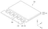
도 1은 본 발명의 실시예에 따른 유기발광표시장치를 보여주는 사시도이다. 도 2는 도 1의 제1 기판, 게이트 구동부, 소스 드라이브 IC, 연성필름, 회로보드, 및 타이밍 제어부를 보여주는 평면도이다.1 is a perspective view illustrating an organic light emitting display according to an embodiment of the present invention. 2 is a plan view showing the first substrate, the gate driver, the source drive IC, the flexible film, the circuit board, and the timing controller of FIG.
도 1 및 도 2를 참조하면, 본 발명의 실시예에 따른 유기발광 표시장치(100)는 표시패널(110), 게이트 구동부(120), 소스 드라이브 집적회로(integrated circuit, 이하 "IC"라 칭함)(130), 연성필름(140), 회로보드(150), 및 타이밍 제어부(160)를 포함한다.1 and 2, an
표시패널(110)은 제1 기판(111)과 제2 기판(112)을 포함한다. 제2 기판(112)은 봉지 기판일 수 있다. 제1 기판(111)과 제2 기판(112)은 플라스틱 또는 유리(glass)일 수 있다.The
제2 기판(112)과 마주보는 제1 기판(111)의 일면 상에는 게이트 라인들, 데이터 라인들, 및 화소들이 형성된다. 화소들은 복수의 서브 화소들을 포함하며, 복수의 서브 화소들은 게이트 라인들과 데이터 라인들의 교차 영역들에 형성된다.On one side of the
복수의 서브 화소들 각각은 적어도 하나의 박막 트랜지스터와 유기발광소자를 포함할 수 있다. 복수의 서브 화소들 각각은 적어도 하나의 박막 트랜지스터가 게이트 라인의 게이트 신호에 의해 턴-온되는 경우 데이터 라인을 통해 데이터 전압을 공급받는다. 복수의 서브 화소들 각각은 데이터 전압에 따라 유기발광소자로 흐르는 전류를 제어하여 유기발광소자를 소정의 밝기로 발광시킨다. 복수의 서브 화소들에 대한 자세한 설명은 도 3 내지 도 8을 결부하여 후술한다.Each of the plurality of sub-pixels may include at least one thin film transistor and an organic light emitting element. Each of the plurality of sub-pixels is supplied with the data voltage through the data line when at least one thin film transistor is turned on by the gate signal of the gate line. Each of the plurality of sub-pixels controls the current flowing to the organic light emitting element according to the data voltage to emit the organic light emitting element at a predetermined brightness. A detailed description of the plurality of sub-pixels will be described later with reference to FIGS. 3 to 8. FIG.
표시패널(110)은 도 2와 같이 화상을 표시하는 표시영역(DA)과 화상을 표시하지 않는 비표시영역(NDA)으로 구분될 수 있다. 표시영역(DA)에는 게이트 라인들, 데이터 라인들, 및 화소들이 형성될 수 있다. 비표시영역(NDA)에는 게이트 구동부(120)와 패드들이 형성될 수 있다.The
게이트 구동부(120)는 타이밍 제어부(160)로부터 입력되는 게이트 제어신호에 따라 게이트 라인들에 게이트 신호들을 공급한다. 게이트 구동부(120)는 표시패널(110)의 표시영역(DA)의 일측 또는 양측 바깥쪽의 비표시영역(DA)에 GIP(gate driver in panel) 방식으로 형성될 수 있다. 또는, 게이트 구동부(120)는 구동 칩으로 제작되어 연성필름에 실장되고 TAB(tape automated bonding) 방식으로 표시패널(110)의 표시영역(DA)의 일측 또는 양측 바깥쪽의 비표시영역(DA)에 부착될 수도 있다.The
소스 드라이브 IC(130)는 타이밍 제어부(160)로부터 디지털 비디오 데이터와 소스 제어신호를 입력받는다. 소스 드라이브 IC(130)는 소스 제어신호에 따라 디지털 비디오 데이터를 아날로그 데이터전압들로 변환하여 데이터 라인들에 공급한다. 소스 드라이브 IC(130)가 구동 칩으로 제작되는 경우, COF(chip on film) 또는 COP(chip on plastic) 방식으로 연성필름(140)에 실장될 수 있다.The
표시패널(110)의 비표시영역(NDA)에는 데이터 패드들과 같은 패드들이 형성될 수 있다. 연성필름(140)에는 패드들과 소스 드라이브 IC(130)를 연결하는 배선들, 패드들과 회로보드(150)의 배선들을 연결하는 배선들이 형성될 수 있다. 연성필름(140)은 이방성 도전 필름(antisotropic conducting film)을 이용하여 패드들 상에 부착되며, 이로 인해 패드들과 연성필름(140)의 배선들이 연결될 수 있다.Pads such as data pads may be formed in the non-display area NDA of the
회로보드(150)는 연성필름(140)들에 부착될 수 있다. 회로보드(150)는 구동 칩들로 구현된 다수의 회로들이 실장될 수 있다. 예를 들어, 회로보드(150)에는 타이밍 제어부(160)가 실장될 수 있다. 회로보드(150)는 인쇄회로보드(printed circuit board) 또는 연성 인쇄회로보드(flexible printed circuit board)일 수 있다.The
타이밍 제어부(160)는 회로보드(150)의 케이블을 통해 외부의 시스템 보드로부터 디지털 비디오 데이터와 타이밍 신호를 입력받는다. 타이밍 제어부(60)는 타이밍 신호에 기초하여 게이트 구동부(120)의 동작 타이밍을 제어하기 위한 게이트 제어신호와 소스 드라이브 IC(130)들을 제어하기 위한 소스 제어신호를 발생한다. 타이밍 제어부(160)는 게이트 제어신호를 게이트 구동부(120)에 공급하고, 소스 제어신호를 소스 드라이브 IC(130)들에 공급한다.The
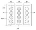
도 3은 도 2의 표시영역의 화소들 일부를 보여주는 평면도이다.3 is a plan view showing a part of pixels of the display area of FIG.
도 3을 참조하면, 표시영역(DA)의 화소(P)들 각각은 도 3과 같이 적색 서브 화소(RP), 녹색 서브 화소(GP), 및 청색 서브 화소(BP)를 포함할 수 있다. 적색 서브 화소(RP)는 적색 광을 발광하는 서브 화소, 녹색 서브 화소(GP)는 녹색 광을 발광하는 서브 화소, 청색 서브 화소(BP)는 청색 광을 발광하는 서브 화소를 나타낸다. 본 발명의 실시예는 화소(P)들 각각이 적색 서브 화소(RP), 녹색 서브 화소(GP), 및 청색 서브 화소(BP)를 포함하는 것에 한정되지 않으며, 화소(P)들의 서브 화소들의 개수와 서브 화소들의 색 조합은 표시패널(110)의 특성에 따라 변경될 수 있다.Referring to FIG. 3, each of the pixels P in the display area DA may include a red subpixel RP, a green subpixel GP, and a blue subpixel BP, as shown in FIG. The red sub-pixel RP represents a sub-pixel for emitting red light, the green sub-pixel GP represents a sub-pixel for emitting green light, and the blue sub-pixel BP represents a sub-pixel for emitting blue light. The embodiment of the present invention is not limited to the case where each of the pixels P includes the red subpixel RP, the green subpixel GP and the blue subpixel BP, The number and the color combination of the sub-pixels may be changed according to the characteristics of the
서브 화소들(RP, GP, BP) 각각은 복수의 발광부들(RE, GE, BE)을 포함할 수 있다. 적색 서브 화소(RP)는 적색 광을 발광하는 복수의 적색 발광부(RE)들을 포함하고, 녹색 서브 화소(GP)는 녹색 광을 발광하는 복수의 녹색 발광부(GE)들을 포함하며, 청색 서브 화소(BP)는 청색 광을 발광하는 복수의 청색 발광부(BE)들을 포함할 수 있다. 복수의 발광부들(RE, GE, BE)은 뱅크(BANK)에 의해 구획된다.Each of the sub pixels RP, GP, and BP may include a plurality of light emitting units RE, GE, and BE. The red sub-pixel RP includes a plurality of red light emitting units RE for emitting red light, the green sub-pixel GP includes a plurality of green light emitting units GE for emitting green light, The pixel BP may include a plurality of blue light emitting portions BE for emitting blue light. The plurality of light emitting units RE, GE, and BE are divided by the banks BANK.
복수의 발광부들(RE, GE, BE) 각각의 유기발광소자는 백색 광을 발광할 수 있다. 이 경우, 복수의 서브 화소들(RP, GP, BP) 각각은 컬러필터를 포함할 수 있다. 또한, 서브 화소들(RP, GP, BP)의 컬러필터들 사이에는 도 3과 같이 혼색을 방지하기 위한 블랙 매트릭스(BM)가 형성될 수 있다. 즉, 서브 화소들(RP, GP, BP)은 블랙 매트릭스(BM)에 의해 구획될 수 있다.The organic light emitting elements of each of the plurality of light emitting units RE, GE, and BE can emit white light. In this case, each of the plurality of sub-pixels RP, GP, BP may include a color filter. In addition, a black matrix BM may be formed between the color filters of the sub-pixels RP, GP, and BP to prevent color mixing as shown in FIG. That is, the sub pixels RP, GP, and BP may be partitioned by a black matrix BM.
복수의 발광부들(RE, GE, BE) 각각의 유기발광소자는 백색 광이 아닌 소정의 색을 갖는 광을 발광할 수 있다. 예를 들어, 적색 발광부(RE)의 유기발광소자가 적색 광을 발광하고, 녹색 발광부(GE)의 유기발광소자가 녹색 광을 발광하며, 청색 발광부(GE)의 유기발광소자가 청색 광을 발광할 수 있다. 이 경우, 복수의 서브 화소들(RP, GP, BP) 각각은 컬러필터를 포함할 필요가 없다.The organic light emitting elements of each of the plurality of light emitting units RE, GE, and BE can emit light having a predetermined color other than white light. For example, when the organic light emitting element of the red light emitting portion RE emits red light, the organic light emitting element of the green light emitting portion GE emits green light, and the organic light emitting element of the blue light emitting portion GE emits blue light Light can be emitted. In this case, each of the plurality of sub pixels RP, GP, BP need not include a color filter.
한편, 도 3에서는 복수의 발광부들(RE, GE, BE)의 평면 형태가 원형인 것을 예시하였으나, 이에 한정되지 않는다. 즉, 복수의 발광부들(RE, GE, BE)의 평면 형태는 삼각형, 사각형, 오각형과 같은 다각형일 수 있다.3, the planar shape of the plurality of light emitting units RE, GE, and BE is circular. However, the present invention is not limited thereto. That is, the plane shape of the plurality of light emitting units RE, GE, and BE may be a polygon such as a triangle, a rectangle, or a pentagon.
이상에서 살펴본 바와 같이, 본 발명의 일 실시예는 복수의 서브 화소들(RP, GP, BP) 각각이 복수의 발광부들(RE, GE, BE)을 포함하며, 복수의 발광부들(RE, GE, BE)은 뱅크(BANK)에 의해 구획된다. 이때, 뱅크(BANK)의 굴절률이 복수의 발광부들(RE, GE, BE)에 형성된 복수의 층들 각각의 굴절률보다 낮은 경우, 유기발광소자로부터 발광된 광이 뱅크(BANK)에 소정의 임계각보다 큰 각도로 입사되는 경우 뱅크(BANK)에 의해 전반사될 수 있다. 즉, 본 발명의 일 실시예는 유기발광소자로부터 뱅크(BANK)로 진행하는 광을 뱅크(BANK)에 의해 전반사하여 상부 기판 방향으로 출광시킴으로써, 유기발광소자로부터 발광된 광의 손실을 줄일 수 있다.As described above, according to an embodiment of the present invention, each of the plurality of sub-pixels RP, GP, and BP includes a plurality of light emitting units RE, GE, and BE, , BE are partitioned by the bank BANK. At this time, when the refractive index of the bank BANK is lower than the refractive index of each of the plurality of layers formed in the plurality of light emitting portions RE, GE, and BE, light emitted from the organic light emitting element is incident on the bank BANK larger than a predetermined critical angle And can be totally reflected by the bank BANK when incident at an angle. That is, in one embodiment of the present invention, the light traveling from the organic light emitting device to the bank is totally reflected by the bank, and the light is emitted toward the upper substrate, thereby reducing loss of light emitted from the organic light emitting device.
이하에서는 도 4 및 도 5를 결부하여 서브 화소들(RP, GP, BP) 각각의 단면 구조를 상세히 살펴본다.Hereinafter, the cross-sectional structure of each of the sub-pixels RP, GP, and BP will be described in detail with reference to FIGS.
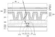
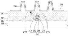
도 4는 도 3의 I-I'의 일 예를 보여주는 단면도이다.4 is a cross-sectional view showing an example of I-I 'of FIG.
도 4를 참조하면, 제2 기판(112)과 마주보는 제1 기판(111)의 일면 상에는 박막트랜지스터(210)들이 형성된다. 박막트랜지스터(210)들 각각은 액티브층(211), 게이트전극(212), 소스전극(215) 및 드레인전극(214)을 포함한다. 도 4에서는 박막트랜지스터(210)들이 게이트전극(212)이 액티브층(211)의 상부에 위치하는 상부 게이트(탑 게이트, top gate) 방식으로 형성된 것을 예시하였으나, 이에 한정되지 않음에 주의하여야 한다. 즉, 박막트랜지스터(210)들은 게이트전극(212)이 액티브층(211)의 하부에 위치하는 하부 게이트(보텀 게이트, bottom gate) 방식 또는 게이트전극(212)이 액티브층(211)의 상부와 하부에 모두 위치하는 더블 게이트(double gate) 방식으로 형성될 수 있다.Referring to FIG. 4,
제1 기판(111) 상에는 액티브층(211)이 형성된다. 액티브층(211)은 실리콘계 반도체 물질 또는 산화물계 반도체 물질로 형성될 수 있다.An
제1 기판(111)과 액티브층(211) 사이에는 액티브층(211)을 보호하고 액티브층(211)의 계면 접착력을 높이기 위한 버퍼막(미도시)이 형성될 수 있다. 버퍼막(미도시)은 실리콘 산화막(SiOx), 실리콘 질화막(SiNx), SiON, 또는 이들의 다중막으로 형성될 수 있다.A buffer layer (not shown) may be formed between the
또한, 제1 기판(111)과 액티브층(211)들 사이에는 액티브층(211)들로 입사되는 외부광을 차단하기 위한 차광층(미도시)이 형성될 수 있다. 차광층(미도시)은 불투명한 금속 물질로 형성될 수 있다.A light shielding layer (not shown) may be formed between the
액티브층(211)들 상에는 게이트 절연막(220)이 형성될 수 있다. 게이트 절연막(220)은 무기막, 예를 들어 실리콘 산화막(SiOx), 실리콘 질화막(SiNx), 또는 이들의 다중막으로 형성될 수 있다.A
게이트 절연막(220) 상에는 게이트 전극(212)들과 게이트 라인들이 형성될 수 있다. 게이트 전극(212)들과 게이트 라인들은 몰리브덴(Mo), 알루미늄(Al), 크롬(Cr), 금(Au), 티타늄(Ti), 니켈(Ni), 네오디뮴(Nd) 및 구리(Cu) 중 어느 하나 또는 이들의 합금으로 이루어진 단일층 또는 다중층으로 형성될 수 있다.
게이트 전극(212)들 상에는 층간 절연막(230)이 형성될 수 있다. 예를 들어, 층간 절연막(230)은 무기막, 예를 들어 실리콘 산화막(SiOx), 실리콘 질화막(SiNx), 또는 이들의 다중막으로 형성될 수 있다.An interlayer insulating
층간 절연막(230) 상에는 소스전극(215)들, 드레인 전극(214)들, 및 데이터 라인들이 형성될 수 있다. 소스전극(215)들 및 드레인전극(214)들 각각은 게이트 절연막(220)과 층간 절연막(230)을 관통하는 콘택홀(CT1)을 통해 액티브층(211)에 접속될 수 있다. 소스전극(215)들, 드레인 전극(214)들, 및 데이터 라인들은 몰리브덴(Mo), 알루미늄(Al), 크롬(Cr), 금(Au), 티타늄(Ti), 니켈(Ni), 네오디뮴(Nd) 및 구리(Cu) 중 어느 하나 또는 이들의 합금으로 이루어진 단일층 또는 다중층으로 형성될 수 있다.
소스전극(215)들, 드레인전극(214)들, 및 데이터 라인들 상에는 박막 트랜지스터(210)들의 상부를 평탄하게 하기 위한 평탄화막(240)이 형성될 수 있다. 평탄화막(240)은 아크릴 수지(acryl resin), 에폭시 수지(epoxy resin), 페놀 수지(phenolic resin), 폴리아미드 수지(polyamide resin), 폴리이미드 수지(polyimide resin) 등의 유기막으로 형성될 수 있다.A
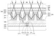
평탄화막(240) 상에는 유기발광소자(250)들을 포함하는 발광부(RE)들이 형성된다. 유기발광소자(250)들 각각은 애노드전극(251), 유기발광층(252), 및 캐소드전극(253)를 포함한다. 발광부(RE)들은 뱅크(255)에 의해 구획된다.On the
평탄화막(240) 상에는 애노드전극(251)이 형성된다. 애노드전극(251)은 평탄화막(240)을 관통하는 콘택홀(CT2)을 통해 드레인전극(214)에 접속된다. 애노드전극(251)은 마이크로 캐비티(micro cavity) 효과를 얻기 위해 알루미늄과 티타늄의 적층 구조(Ti/Al/Ti), 알루미늄과 ITO의 적층 구조(ITO/Al/ITO), APC 합금, 및 APC 합금과 ITO의 적층 구조(ITO/APC/ITO)과 같은 반사율이 높은 금속물질로 형성될 수 있다. APC 합금은 은(Ag), 팔라듐(Pd), 및 구리(Cu)의 합금이다.An
뱅크(255)는 발광부(RE)들을 구획하기 위해 애노드전극(251) 상에 형성될 수 있다. 뱅크(255)는 유기발광층(252)에서 발광된 광(L)을 전반사시키기 위해 유기발광층(252)보다 낮은 굴절률을 갖는 유기물질로 형성될 수 있다. 예를 들어, 뱅크(255)는 1.6 이하의 굴절률을 가지는 유기물질로 형성될 수 있으며, 포토 아크릴계 물질로 형성될 수 있다. 또한, 유기발광층(252)에서 발광된 광(L)이 뱅크(255)에 의해 전반사되는 비율을 높이기 위해 뱅크(255)의 높이는 3㎛ 이상으로 형성되는 것이 바람직하다.The
애노드전극(251)과 뱅크(255) 상에는 유기발광층(252)이 형성된다. 유기발광층(252)은 정공 수송층(hole transporting layer), 발광층(light emitting layer), 및 전자 수송층(electron transporting layer)을 포함할 수 있다. 이 경우, 애노드전극(251)과 캐소드전극(253)에 전압이 인가되면 정공과 전자가 각각 정공 수송층과 전자 수송층을 통해 발광층으로 이동하게 되며, 발광층에서 서로 결합하여 발광하게 된다.An organic
유기발광층(252)은 백색 광을 발광하는 백색 발광층만을 포함할 수 있다. 유기발광층(252)이 백색 발광층인 경우, 도 4와 같이 애노드 전극(251)들과 뱅크(255)를 덮도록 형성될 수 있다.The organic
또는, 유기발광층(252)은 적색 광을 발광하는 적색 발광층, 녹색 광을 발광하는 녹색 발광층, 청색 광을 발광하는 청색 발광층을 포함할 수 있다. 이 경우, 적색 발광층은 적색 발광부(RE)의 애노드전극(251) 상에 형성되고, 녹색 발광층은 녹색 발광부(GE)의 애노드전극(251) 상에 형성되며, 청색 발광층은 청색 발광부(BE)의 애노드전극(251) 상에 형성될 수 있다.Alternatively, the organic
유기발광층(252)은 대략 1.8 이상의 굴절률을 갖는 유기물질로 형성될 수 있다.The organic
캐소드전극(253)은 유기발광층(252) 상에 형성된다. 캐소드전극(253)은 광을 투과시킬 수 있는 ITO, IZO와 같은 투명한 금속물질(TCO, Transparent Conductive Material)로 형성되거나, 또는 마그네슘(Mg), 은(Ag), 또는 마그네슘(Mg)과 은(Ag)의 합금과 같은 반투과 금속물질(Semi-transmissive Conductive Material)로 형성될 수 있다.The
캐소드전극(253) 상에는 캡핑층(capping layer, 미도시)이 형성될 수 있다. 캡핑층(미도시)은 대략 1.8 이상의 굴절률을 갖는 유기물질로 형성될 수 있으며, 유기발광층(252)의 굴절률과 매칭되는 유기물질로 형성되는 것이 바람직하다. 캡핑층(미도시)은 생략될 수 있다.A capping layer (not shown) may be formed on the
캐소드전극(253) 상에는 봉지막(260)이 형성된다. 봉지막(260)은 유기발광층(252)과 캐소드전극(253)에 산소 또는 수분이 침투되는 것을 방지하는 역할을 한다. 이를 위해, 봉지막(260)은 적어도 하나의 무기막과 적어도 하나의 유기막을 포함할 수 있다. 도 3에서는 봉지층(260)이 제1 무기막(261), 유기막(262) 및 제2 무기막(263)을 포함하는 것을 예시하였으나, 이에 한정되지 않는다.A sealing
제1 무기막(261)은 캐소드전극(253)을 덮도록 캐소드전극(253) 상에 형성된다. 유기막(262)은 이물들(particles)이 제1 무기막(261)을 뚫고 유기발광층(252)과 캐소드전극(253)에 투입되는 것을 방지하기 위해 제1 무기막(261) 상에 형성된다. 제2 무기막(263)은 유기막(262)을 덮도록 유기막(262) 상에 형성된다.The first
제1 및 제2 무기막들(261, 263) 각각은 실리콘 질화물, 알루미늄 질화물, 지르코늄 질화물, 티타늄 질화물, 하프늄 질화물, 탄탈륨 질화물, 실리콘 산화물, 알루미늄 산화물 또는 티타늄 산화물로 형성될 수 있다. 제1 무기막(261)은 대략 1.8 이상의 굴절률을 갖는 유기물질로 형성될 수 있으며, 유기발광층(252)의 굴절률과 매칭되는 유기물질로 형성되는 것이 바람직하다.Each of the first and second
유기막(262)은 유기발광층(253)에서 발광된 광(L)을 통과시키기 위해 투명하게 형성될 수 있다. 유기막(262)은 유기발광층(253)에서 발광된 광(L)을 99% 이상 통과시킬 수 있는 유기물질로 형성되는 것이 바람직하다.The
또한, 유기막(262)은 뱅크(255)의 높이로 인해 발생된 뱅크(255)와 발광부(RE) 사이의 단차를 평탄화하기 위해 뱅크(255) 사이의 공간을 채우도록 형성된다. 유기막(262)은 대략 1.8 이상의 굴절률을 갖는 유기물질로 형성될 수 있으며, 유기발광층(252)의 굴절률과 매칭되는 유기물질로 형성되는 것이 바람직하다. 이를 위해, 유기막(262)은 바이닐 화합물(vinyl compound), 광중합 개시제(Photopolymerization initiator), 톨루엔(Toluene), 및 2,6-디-tert-부틸-4-메틸페놀(2,6-di-tert-butyl-4-methylphenol)을 포함할 수 있다. 이 경우, 바이닐 화합물은 황화 페닐(phenyl sulfide)일 수 있다.The
제1 기판(111)과 마주보는 제2 기판(112) 상에는 컬러필터(RC)들과 블랙 매트릭스(BM)가 형성될 수 있다. 적색 서브화소(RP)에는 적색 컬러필터(RC)가 형성되고, 녹색 서브화소(GP)에는 녹색 컬러필터가 형성되며, 청색 서브화소(BP)에는 청색 컬러필터가 형성될 수 있다. 블랙 매트릭스(BM)는 서로 다른 색을 갖는 컬러필터들 사이에 배치될 수 있다. 이로 인해, 블랙 매트릭스(BM)는 서브화소들(RP, GP, BP)을 구획하는 역할을 한다.Color filters (RC) and a black matrix (BM) may be formed on the
유기발광층(252)이 적색 광을 발광하는 적색 발광층, 녹색 광을 발광하는 녹색 발광층, 청색 광을 발광하는 청색 발광층을 포함하는 경우, 컬러필터(RC)들과 블랙 매트릭스(BM)는 생략될 수 있다.When the organic
제1 기판(111)의 봉지층(260)과 제2 기판(112)의 컬러필터(RC)들은 접착층(270)을 이용하여 접착되며, 이로 인해 제1 기판(111)과 제2 기판(112)은 합착될 수 있다. 접착층(270)은 투명한 접착 레진일 수 있다.The
이상에서 살펴본 바와 같이, 본 발명의 일 실시예는 유기발광층(252)과 봉지층(260)의 제1 무기막(261) 및 유기막(262)을 1.8 이상의 굴절률로 형성하고, 뱅크(255)를 1.6 이하의 굴절률로 형성한다. 특히, 유기발광층(252), 제1 무기막(261) 및 유기막(262) 각각의 굴절률과 뱅크(255)의 굴절률 간의 차이가 클수록 유기발광층(252)에서 발광된 광(L)이 뱅크(255)에 의해 전반사되는 전반사율이 높아질 수 있다. 또한, 전반사율을 높이기 위해서는 유기발광층(252), 제1 무기막(261) 및 유기막(262)은 동일한 굴절률을 갖는 것이 바람직하다.The first
결국, 본 발명의 실시예는 유기발광층(252)의 굴절률과 제1 무기막(261)의 굴절률 간의 차이가 유기발광층(252)의 굴절률과 뱅크(255)의 굴절률 간의 차이 및 제1 무기막(261)의 굴절률과 뱅크(255)의 굴절률 간의 차이보다 작게 한다. 또한, 유기발광층(252)의 굴절률과 유기막(262)의 굴절률 간의 차이가 유기발광층(252)의 굴절률과 뱅크(255)의 굴절률 간의 차이 및 유기막(262)의 굴절률과 뱅크(255)의 굴절률 간의 차이보다 작게 한다. 이 경우, 유기발광층(252)으로부터 뱅크(255)로 진행하는 광은 고굴절 매질에서 저굴절 매질로 진행하게 되므로, 소정의 임계각 이상의 각도로 뱅크(255)로 입사되는 경우, 뱅크(255)의 경계에서 전반사된다. 따라서, 본 발명의 일 실시예는 유기발광층(252)으로부터 뱅크(255)로 진행하는 광을 뱅크(255)에 의해 전반사하여 상부 기판 방향으로 출광시킬 수 있으므로, 유기발광층(252)으로부터 발광된 광(L)의 손실을 줄일 수 있다.The difference between the refractive index of the organic
또한, 본 발명의 일 실시예는 뱅크(255)에 의한 전반사 효과를 높이기 위해 뱅크(255)의 높이를 3㎛ 이상으로 형성하며, 이 경우 뱅크(255)의 높이로 인해 뱅크(255)와 발광부(RE) 사이에 단차가 발생할 수 있다. 본 발명의 일 실시예는 봉지층(260)을 이용하여 뱅크(255) 사이의 공간을 채움으로써 뱅크(255)와 발광부(RE) 사이에 단차를 평탄화할 수 있다. 특히, 본 발명은 뱅크(255) 사이의 공간을 채우는 유기물질을 유기발광층(252)의 굴절률과 매칭되도록 함으로써 유기발광층(252)으로부터 뱅크(255)로 진행하는 광을 뱅크(255)에 의해 전반사하여 상부 기판(112) 방향으로 출광시킬 수 있다.In order to increase the total reflection effect by the
도 5는 도 3의 I-I'의 또 다른 예를 보여주는 단면도이다.5 is a cross-sectional view showing another example of I-I 'of FIG.
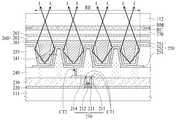
도 5에서는 뱅크(255)와 발광부(RE) 사이의 단차를 평탄화하기 위해 뱅크(255) 사이의 공간을 유기막(262)이 아닌 제1 무기막(261)으로 채우는 것을 제외하고는 도 4를 결부하여 설명한 바와 실질적으로 동일하다. 그러므로, 도 5의 단면도에 대한 자세한 설명은 생략한다.5, except that the space between the
도 6은 도 2의 표시영역의 화소들 일부를 보여주는 또 다른 평면도이다.6 is another plan view showing a part of pixels of the display area of FIG.
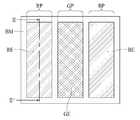
도 6을 참조하면, 표시영역(DA)의 화소(P)들 각각은 도 3과 같이 적색 서브 화소(RP), 녹색 서브 화소(GP), 및 청색 서브 화소(BP)를 포함할 수 있다. 적색 서브 화소(RP)는 적색 광을 발광하는 서브 화소, 녹색 서브 화소(GP)는 녹색 광을 발광하는 서브 화소, 청색 서브 화소(BP)는 청색 광을 발광하는 서브 화소를 나타낸다. 본 발명의 실시예는 화소(P)들 각각이 적색 서브 화소(RP), 녹색 서브 화소(GP), 및 청색 서브 화소(BP)를 포함하는 것에 한정되지 않으며, 화소(P)들의 서브 화소들의 개수와 서브 화소들의 색 조합은 표시패널(10)의 특성에 따라 변경될 수 있다.Referring to FIG. 6, each of the pixels P in the display area DA may include a red subpixel RP, a green subpixel GP, and a blue subpixel BP, as shown in FIG. The red sub-pixel RP represents a sub-pixel for emitting red light, the green sub-pixel GP represents a sub-pixel for emitting green light, and the blue sub-pixel BP represents a sub-pixel for emitting blue light. The embodiment of the present invention is not limited to the case where each of the pixels P includes the red subpixel RP, the green subpixel GP and the blue subpixel BP, The number and the color combination of the sub-pixels may be changed according to the characteristics of the display panel 10. [
서브 화소들(RP, GP, BP) 각각은 하나의 발광부를 포함할 수 있다. 적색 서브 화소(RP)는 적색 광을 발광하는 하나의 적색 발광부(RE)를 포함하고, 녹색 서브 화소(GP)는 녹색 광을 발광하는 하나의 녹색 발광부(GE)를 포함하며, 청색 서브 화소(BP)는 청색 광을 발광하는 하나의 청색 발광부(BE)를 포함할 수 있다. 발광부들은 뱅크(미도시)에 의해 구획될 수 있다.Each of the sub pixels RP, GP, and BP may include one light emitting portion. The red sub-pixel RP includes one red light emitting portion RE for emitting red light, the green sub-pixel GP includes one green light emitting portion GE for emitting green light, The pixel BP may include one blue light emitting portion BE for emitting blue light. The light emitting portions may be partitioned by a bank (not shown).
각 발광부의 유기발광소자는 백색 광을 발광할 수 있다. 이 경우, 복수의 서브 화소들(RP, GP, BP) 각각은 컬러필터를 포함할 수 있다. 또한, 서브 화소들(RP, GP, BP)의 컬러필터들 사이에는 도 6과 같이 혼색을 방지하기 위한 블랙 매트릭스(BM)가 형성될 수 있다. 블랙 매트릭스(BM)는 뱅크(미도시) 상에 형성될 수 있다.The organic light emitting element of each light emitting portion can emit white light. In this case, each of the plurality of sub-pixels RP, GP, BP may include a color filter. In addition, a black matrix BM may be formed between the color filters of the sub-pixels RP, GP, and BP to prevent color mixing as shown in FIG. The black matrix BM may be formed on a bank (not shown).
각 발광부의 유기발광소자는 백색 광이 아닌 소정의 색을 갖는 광을 발광할 수 있다. 예를 들어, 적색 발광부(RE)의 유기발광소자가 적색 광을 발광하고, 녹색 발광부(GE)의 유기발광소자가 녹색 광을 발광하며, 청색 발광부(GE)의 유기발광소자가 청색 광을 발광할 수 있다. 이 경우, 복수의 서브 화소들(RP, GP, BP) 각각은 컬러필터를 포함할 필요가 없다.The organic light emitting element of each light emitting portion can emit light having a predetermined color other than white light. For example, when the organic light emitting element of the red light emitting portion RE emits red light, the organic light emitting element of the green light emitting portion GE emits green light, and the organic light emitting element of the blue light emitting portion GE emits blue light Light can be emitted. In this case, each of the plurality of sub pixels RP, GP, BP need not include a color filter.
이상에서 살펴본 바와 같이, 본 발명의 일 실시예는 복수의 서브 화소들(RP, GP, BP) 각각이 하나의 발광부를 포함하며, 발광부들은 뱅크(미도시)에 의해 구획된다. 이때, 뱅크(미도시)의 굴절률이 하나의 발광부에 형성된 복수의 층들 각각의 굴절률보다 낮은 경우, 유기발광소자로부터 발광된 광이 뱅크(미도시)에 소정의 임계각보다 큰 각도로 입사되는 경우 뱅크(미도시)에 의해 전반사될 수 있다. 즉, 본 발명의 실시예는 유기발광소자로부터 뱅크(미도시)로 진행하는 광을 뱅크(미도시)에 의해 전반사하여 상부 기판 방향으로 출광시킴으로써, 유기발광소자로부터 발광된 광의 손실을 줄일 수 있다.As described above, in one embodiment of the present invention, each of the plurality of sub pixels RP, GP, and BP includes one light emitting unit, and the light emitting units are divided by a bank (not shown). In this case, when the refractive index of the bank (not shown) is lower than the refractive index of each of the plurality of layers formed in one light emitting portion, when light emitted from the organic light emitting element is incident on the bank (not shown) at an angle larger than a predetermined critical angle May be totally reflected by a bank (not shown). That is, in the embodiment of the present invention, light traveling from the organic light emitting element to the bank (not shown) is totally reflected by a bank (not shown) and is emitted toward the upper substrate, thereby reducing the loss of light emitted from the organic light emitting element .
이하에서는 도 7 및 도 8을 결부하여 서브 화소들(RP, GP, BP) 각각의 단면 구조를 상세히 살펴본다.Hereinafter, the cross-sectional structure of each of the sub-pixels RP, GP, and BP will be described in detail with reference to FIGS. 7 and 8. FIG.
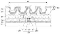
도 7은 도 3의 Ⅱ-Ⅱ'의 일 예를 보여주는 단면도이다.7 is a cross-sectional view showing an example of II-II 'of FIG.
도 7에 도시된 제1 기판(111), 박막 트랜지스터(210), 게이트 절연막(220), 및 층간 절연막(230)은 도 4를 결부하여 설명한 바와 실질적으로 동일하므로, 이들에 대한 자세한 설명은 생략한다.Since the
도 7을 참조하면, 소스전극(215)들, 드레인전극(214)들, 및 데이터 라인들 상에는 박막 트랜지스터(210)들의 상부를 평탄하게 하기 위한 평탄화막(240)이 형성될 수 있다. 평탄화막(240)은 아크릴 수지(acryl resin), 에폭시 수지(epoxy resin), 페놀 수지(phenolic resin), 폴리아미드 수지(polyamide resin), 폴리이미드 수지(polyimide resin) 등의 유기막으로 형성될 수 있다.Referring to FIG. 7, a
평탄화막(240)은 평탄화막(240)으로부터 돌출된 양각 패턴(241)을 포함한다. 양각 패턴(241)은 뱅크(255) 사이에 배치되도록 형성될 수 있다. 또한, 양각 패턴(241)의 높이는 뱅크(255)의 높이보다 낮거나 같을 수 있다. 양각 패턴(241)의 높이가 뱅크(255)의 높이보다 높아지는 경우, 양각 패턴(241) 사이의 공간을 채워 양각 패턴(241)으로 인한 단차를 평탄화하기 위한 봉지층(260)의 두께가 두꺼워진다. 따라서, 양각 패턴(241)의 높이는 뱅크(255)의 높이보다 낮거나 같은 것이 바람직하다.The
평탄화막(240) 상에는 유기발광소자(250)들을 포함하는 발광부(RE)들이 형성된다. 유기발광소자(250)들 각각은 애노드전극(251), 유기발광층(252), 및 캐소드전극(253)를 포함한다. 발광부(RE)들은 뱅크(255)에 의해 구획된다.On the
평탄화막(240) 상에는 애노드전극(251)이 형성된다. 애노드전극(251)은 평탄화막(240)을 관통하는 콘택홀(CT2)을 통해 드레인전극(214)에 접속된다. 애노드전극(251)은 마이크로 캐비티(micro cavity) 효과를 얻기 위해 알루미늄, 알루미늄과 몰리브덴의 적층 구조(Mo/Al/Mo), 알루미늄과 티타늄의 적층 구조(Ti/Al/Ti), 알루미늄과 ITO의 적층 구조(ITO/Al/ITO), APC 합금, 및 APC 합금과 ITO의 적층 구조(ITO/APC/ITO)과 같은 반사율이 높은 금속물질로 형성될 수 있다. APC 합금은 은(Ag), 팔라듐(Pd), 및 구리(Cu)의 합금이다.An
애노드전극(251)은 평탄화막(240)의 양각 패턴(241) 상에도 형성된다. 이로 인해, 애노드전극(251)은 유기발광층(252)으로부터 양각 패턴(241)으로 진행하는 광을 애노드전극(251)에 의해 전반사하여 상부 기판 방향으로 출광시킬 수 있으므로, 본 발명의 일 실시예는 유기발광층(252)으로부터 발광된 광(L)의 손실을 줄일 수 있다.The
뱅크(255)는 발광부(RE)들을 구획하기 위해 애노드전극(251)의 가장자리를 덮도록 형성될 수 있다. 뱅크(255)는 유기발광층(252)에서 발광된 광(L)을 전반사시키기 위해 유기발광층(252)보다 낮은 굴절률을 갖는 유기물질로 형성될 수 있다. 예를 들어, 뱅크(255)는 1.6 이하의 굴절률을 가지는 유기물질로 형성될 수 있으며, 포토 아크릴계 물질로 형성될 수 있다. 또한, 유기발광층(252)에서 발광된 광(L)이 뱅크(255)에 의해 전반사되는 비율을 높이기 위해 뱅크(255)의 높이는 3㎛ 이상으로 형성되는 것이 바람직하다.The
평탄화층(240)은 애노드전극(251) 아래에 배치되는 반면에, 뱅크(255)는 애노드전극(251) 상에 형성된다. 따라서, 평탄화층(240)과 뱅크(255)는 별도의 공정으로 형성되며, 이로 인해 서로 다른 물질로 형성될 수 있다.The
애노드전극(251)과 뱅크(255) 상에는 유기발광층(252)이 형성된다. 유기발광층(252)은 정공 수송층(hole transporting layer), 발광층(light emitting layer), 및 전자 수송층(electron transporting layer)을 포함할 수 있다. 이 경우, 애노드전극(251)과 캐소드전극(253)에 전압이 인가되면 정공과 전자가 각각 정공 수송층과 전자 수송층을 통해 발광층으로 이동하게 되며, 발광층에서 서로 결합하여 발광하게 된다.An organic
유기발광층(252)은 백색 광을 발광하는 백색 발광층만을 포함할 수 있다. 유기발광층(252)이 백색 발광층인 경우, 도 4와 같이 애노드 전극(251)들과 뱅크(255)를 덮도록 형성될 수 있다.The organic
또는, 유기발광층(252)은 적색 광을 발광하는 적색 발광층, 녹색 광을 발광하는 녹색 발광층, 청색 광을 발광하는 청색 발광층을 포함할 수 있다. 이 경우, 적색 발광층은 적색 발광부(RE)의 애노드전극(251) 상에 형성되고, 녹색 발광층은 녹색 발광부(GE)의 애노드전극(251) 상에 형성되며, 청색 발광층은 청색 발광부(BE)의 애노드전극(251) 상에 형성될 수 있다.Alternatively, the organic
유기발광층(252)은 대략 1.8 이상의 굴절률을 갖는 유기물질로 형성될 수 있다.The organic
캐소드전극(253)은 유기발광층(252) 상에 형성된다. 캐소드전극(253)은 광을 투과시킬 수 있는 ITO, IZO와 같은 투명한 금속물질(TCO, Transparent Conductive Material)로 형성되거나, 또는 마그네슘(Mg), 은(Ag), 또는 마그네슘(Mg)과 은(Ag)의 합금과 같은 반투과 금속물질(Semi-transmissive Conductive Material)로 형성될 수 있다.The
캐소드전극(253) 상에는 캡핑층(capping layer, 미도시)이 형성될 수 있다. 캡핑층(미도시)은 대략 1.8 이상의 굴절률을 갖는 유기물질로 형성될 수 있으며, 유기발광층(252)의 굴절률과 매칭되는 유기물질로 형성되는 것이 바람직하다. 캡핑층(미도시)은 생략될 수 있다.A capping layer (not shown) may be formed on the
캐소드전극(253) 상에는 봉지막(260)이 형성된다. 봉지막(260)은 유기발광층(252)과 캐소드전극(253)에 산소 또는 수분이 침투되는 것을 방지하는 역할을 한다. 이를 위해, 봉지막(260)은 적어도 하나의 무기막과 적어도 하나의 유기막을 포함할 수 있다. 도 3에서는 봉지층(260)이 제1 무기막(261), 유기막(262) 및 제2 무기막(263)을 포함하는 것을 예시하였으나, 이에 한정되지 않는다.A sealing
제1 무기막(261)은 캐소드전극(253)을 덮도록 캐소드전극(253) 상에 형성된다. 유기막(262)은 이물들(particles)이 제1 무기막(261)을 뚫고 유기발광층(252)과 캐소드전극(253)에 투입되는 것을 방지하기 위해 제1 무기막(261) 상에 형성된다. 제2 무기막(263)은 유기막(262)을 덮도록 유기막(262) 상에 형성된다.The first
제1 및 제2 무기막들(261, 263) 각각은 실리콘 질화물, 알루미늄 질화물, 지르코늄 질화물, 티타늄 질화물, 하프늄 질화물, 탄탈륨 질화물, 실리콘 산화물, 알루미늄 산화물 또는 티타늄 산화물로 형성될 수 있다. 제1 무기막(261)은 대략 1.8 이상의 굴절률을 갖는 유기물질로 형성될 수 있으며, 유기발광층(252)의 굴절률과 매칭되는 유기물질로 형성되는 것이 바람직하다.Each of the first and second
유기막(262)은 유기발광층(253)에서 발광된 광(L)을 통과시키기 위해 투명하게 형성될 수 있다. 유기막(262)은 유기발광층(253)에서 발광된 광(L)을 99% 이상 통과시킬 수 있는 유기물질로 형성되는 것이 바람직하다.The
또한, 유기막(262)은 평탄화막(240)의 양각 패턴(241)과 뱅크(255)의 높이로 인해 발생된 양각 패턴(241) 사이의 단차를 평탄화하기 위해 뱅크(255) 사이의 공간을 채우도록 형성된다. 유기막(262)은 대략 1.8 이상의 굴절률을 갖는 유기물질로 형성될 수 있으며, 유기발광층(252)의 굴절률과 매칭되는 유기물질로 형성되는 것이 바람직하다. 이를 위해, 유기막(262)은 바이닐 화합물(vinyl compound), 광중합 개시제(Photopolymerization initiator), 톨루엔(Toluene), 및 2,6-디-tert-부틸-4-메틸페놀(2,6-di-tert-butyl-4-methylphenol)을 포함할 수 있다. 이 경우, 바이닐 화합물은 황화 페닐(phenyl sulfide)일 수 있다.The
제1 기판(111)과 마주보는 제2 기판(112) 상에는 컬러필터(RC)들과 블랙 매트릭스(BM)가 형성될 수 있다. 적색 서브화소(RP)에는 적색 컬러필터(RC)가 형성되고, 녹색 서브화소(GP)에는 녹색 컬러필터가 형성되며, 청색 서브화소(BP)에는 청색 컬러필터가 형성될 수 있다. 블랙 매트릭스(BM)는 서로 다른 색을 갖는 컬러필터들 사이에 배치될 수 있다. 이로 인해, 블랙 매트릭스(BM)는 서브화소들(RP, GP, BP)을 구획하는 역할을 한다.Color filters (RC) and a black matrix (BM) may be formed on the
유기발광층(252)이 적색 광을 발광하는 적색 발광층, 녹색 광을 발광하는 녹색 발광층, 청색 광을 발광하는 청색 발광층을 포함하는 경우, 컬러필터(RC)들과 블랙 매트릭스(BM)는 생략될 수 있다.When the organic
제1 기판(111)의 봉지층(260)과 제2 기판(112)의 컬러필터(RC)들은 접착층(270)을 이용하여 접착되며, 이로 인해 제1 기판(111)과 제2 기판(112)은 합착될 수 있다. 접착층(270)은 투명한 접착 레진일 수 있다.The
이상에서 살펴본 바와 같이, 본 발명의 일 실시예는 유기발광층(252)과 봉지층(260)의 제1 무기막(261) 및 유기막(262)을 1.8 이상의 굴절률로 형성하고, 뱅크(255)를 1.6 이하의 굴절률로 형성한다. 특히, 유기발광층(252), 제1 무기막(261) 및 유기막(262) 각각의 굴절률과 뱅크(255)의 굴절률 간의 차이가 클수록 유기발광층(252)에서 발광된 광(L)이 뱅크(255)에 의해 전반사되는 전반사율이 높아질 수 있다. 또한, 전반사율을 높이기 위해서는 유기발광층(252), 제1 무기막(261) 및 유기막(262)은 동일한 굴절률을 갖는 것이 바람직하다.The first
결국, 본 발명의 실시예는 유기발광층(252)의 굴절률과 제1 무기막(261)의 굴절률 간의 차이가 유기발광층(252)의 굴절률과 뱅크(255)의 굴절률 간의 차이 및 제1 무기막(261)의 굴절률과 뱅크(255)의 굴절률 간의 차이보다 작게 한다. 또한, 유기발광층(252)의 굴절률과 유기막(262)의 굴절률 간의 차이가 유기발광층(252)의 굴절률과 뱅크(255)의 굴절률 간의 차이 및 유기막(262)의 굴절률과 뱅크(255)의 굴절률 간의 차이보다 작게 한다. 이 경우, 유기발광층(252)으로부터 뱅크(255)로 진행하는 광은 고굴절 매질에서 저굴절 매질로 진행하게 되므로, 소정의 임계각 이상의 각도로 뱅크(255)로 입사되는 경우, 뱅크(255)의 경계에서 전반사된다. 따라서, 본 발명의 일 실시예는 유기발광층(252)으로부터 뱅크(255)로 진행하는 광을 뱅크(255)에 의해 전반사하여 상부 기판 방향으로 출광시킬 수 있으므로, 유기발광층(252)으로부터 발광된 광(L)의 손실을 줄일 수 있다.The difference between the refractive index of the organic
또한, 본 발명의 일 실시예는 뱅크(255)와 양각 패턴(241)에 의한 전반사 효과를 높이기 위해 뱅크(255)의 높이를 3㎛ 이상으로 형성하고 양각 패턴(241)의 높이를 뱅크(255)의 높이보다 낮거나 동일하게 형성할 수 있다. 이 경우, 뱅크(255)와 양각 패턴(241)의 높이로 인해 단차가 발생할 수 있다. 본 발명의 일 실시예는 봉지층(260)을 이용하여 뱅크(255) 사이의 공간과 양각 패턴(241) 사이의 공간을 채움으로써 상기 단차를 평탄화할 수 있다. 특히, 본 발명은 뱅크(255) 사이의 공간과 양각 패턴(241) 사이의 공간을 채우는 유기물질을 유기발광층(252)의 굴절률과 매칭되도록 함으로써 유기발광층(252)으로부터 뱅크(255)로 진행하는 광을 뱅크(255)에 의해 전반사하여 상부 기판(112) 방향으로 출광시킬 수 있다.In order to increase the total reflection effect by the
나아가, 본 발명의 일 실시예는 평탄화막(240)이 양각 패턴(241)을 포함하며, 양각 패턴(241) 상에 애노드전극(251)을 형성한다. 본 발명의 실시예는 애노드전극(251)을 반사율이 높은 금속물질로 형성하므로, 유기발광층(252)으로부터 양각 패턴(241)으로 진행하는 광을 애노드전극(251)에 의해 전반사하여 상부 기판 방향으로 출광시킬 수 있으므로, 유기발광층(252)으로부터 발광된 광(L)의 손실을 줄일 수 있다. 또한, 애노드전극(251)은 반사율이 높은 금속물질이므로, 뱅크(255)의 굴절률 차이로 인한 전반사보다 높은 전반사 효과를 얻을 수 있다.Further, in one embodiment of the present invention, the
도 8은 도 3의 Ⅱ-Ⅱ'의 또 다른 예를 보여주는 단면도이다.8 is a cross-sectional view showing another example of II-II 'of FIG.
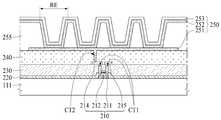
도 8에서는 뱅크(255)와 발광부(RE) 사이의 단차를 평탄화하기 위해 뱅크(255) 사이의 공간을 유기막(262)이 아닌 제1 무기막(261)으로 채우는 것을 제외하고는 도 7을 결부하여 설명한 바와 실질적으로 동일하다. 그러므로, 도 8의 단면도에 대한 자세한 설명은 생략한다.7A and 7B except that the space between the
도 9는 본 발명의 일 실시예에 따른 유기발광표시장치의 제조방법을 보여주는 흐름도이다. 도 10a 내지 도 10e는 본 발명의 일 실시예에 따른 유기발광표시장치의 제조방법을 설명하기 위한 I-I'의 단면도들이다. 도 10a 내지 도 10e에 도시된 단면도들은 전술한 도 4에 도시된 유기발광표시장치의 제조방법에 관한 것이므로, 동일한 구성에 대해 동일한 도면부호를 부여하였다. 이하에서는 도 9 및 도 10a 내지 도 10e를 결부하여 본 발명의 일 실시예에 따른 유기발광표시장치의 제조방법을 상세히 설명한다.9 is a flowchart illustrating a method of manufacturing an OLED display according to an embodiment of the present invention. FIGS. 10A to 10E are cross-sectional views taken along the line I-I 'for explaining a method of manufacturing an organic light emitting display according to an embodiment of the present invention. 10A to 10E relate to the manufacturing method of the organic light emitting diode display shown in FIG. 4 described above, and therefore the same reference numerals are given to the same components. Hereinafter, a method of manufacturing an OLED display according to an embodiment of the present invention will be described in detail with reference to FIGS. 9 and 10A to 10E.
첫 번째로, 도 10a와 같이 제1 기판(111) 상에 박막 트랜지스터(210)들을 형성하고, 박막 트랜지스터(210)들의 상부를 평탄하게 하기 위한 평탄화막(240)을 형성하며, 평탄화막(240) 상에 애노드전극(251)을 형성한다.First, as shown in FIG. 10A, the
구체적으로, 제1 기판(100) 상에 액티브층(110)을 형성하고, 액티브층(211) 상에 게이트 절연막(220)을 형성하며, 게이트 절연막(220) 상에 게이트 전극(212)들과 게이트 라인들을 형성하고, 게이트 전극(212)들 상에 층간 절연막(230)을 형성하며, 층간 절연막(230) 상에 소스전극(215)들, 드레인 전극(214)들, 및 데이터 라인들을 형성한다. 소스전극(215)들 및 드레인전극(214)들 각각은 게이트 절연막(220)과 층간 절연막(230)을 관통하는 콘택홀(CT1)을 통해 액티브층(211)에 접속될 수 있다.More specifically, an
그리고 나서, 소스전극(215)들, 드레인전극(214)들, 및 데이터 라인들 상에 박막 트랜지스터(210)들의 상부를 평탄하게 하기 위한 평탄화막(240)을 형성한다.Then, a
그리고 나서, 평탄화막(240) 상에는 애노드전극(251)이 형성된다. 애노드전극(251)은 평탄화막(240)을 관통하는 콘택홀(CT2)을 통해 드레인전극(214)에 접속된다. (도 9의 S101)Then, an
두 번째로, 도 10b와 같이 발광부들을 구획하기 위해 애노드전극(251) 상에 뱅크(255)를 형성한다.Second, a
뱅크(255)는 유기발광층(252)에서 발광된 광을 전반사시키기 위해 유기발광층(252)보다 낮은 굴절률을 갖는 유기물질로 형성될 수 있다. 예를 들어, 뱅크(255)는 1.6 이하의 굴절률을 가지는 유기물질로 형성될 수 있다. 또한, 유기발광층(252)에서 발광된 광이 뱅크(255)에 의해 전반사되는 비율을 높이기 위해 뱅크(255)의 높이는 3㎛ 이상으로 형성되는 것이 바람직하다.The
뱅크(255)는 스핀 코팅(spin coating) 방식 또는 슬릿 코팅(slit coating) 방식으로 애노드 전극(251) 상에 유기물질을 도포한 후 포토 공정을 노광하여 형성될 수 있다. 스핀 코팅 방식으로 유기물질을 도포하는 경우 유기물질의 점도는 대략 30cp 내지 100cp인 것이 바람직하다. 슬릿 코팅 방식으로 유기물질을 도포하는 경우 유기물질의 점도는 대략 10cp 이하인 것이 바람직하다. (도 9의 S102)The
세 번째로, 도 10c와 같이 애노드 전극(251)과 뱅크(255) 상에 유기발광층(252)과 캐소드전극(253)을 형성한다.Third, an organic
유기발광층(252)은 증착 공정 또는 용액 공정으로 형성될 수 있다. 유기발광층(252)이 증착 공정으로 형성되는 경우, 증발법(Evaporation)을 이용하여 형성될 수 있다. 유기발광층(252)은 대략 1.8 이상의 굴절률을 갖는 유기물질로 형성될 수 있다.The organic
캐소드전극(253)은 스퍼터링(Sputtering)과 같은 증착 공정을 통해 형성될 수 있다. 캐소드전극(253)은 광을 투과시킬 수 있는 ITO, IZO와 같은 투명한 금속물질(TCO, Transparent Conductive Material)로 형성되거나, 또는 마그네슘(Mg), 은(Ag), 또는 마그네슘(Mg)과 은(Ag)의 합금과 같은 반투과 금속물질(Semi-transmissive Conductive Material)로 형성될 수 있다. (도 9의 S103)The
네 번째로, 도 10d와 같이 캐소드전극(253) 상에 봉지층(260)을 형성한다. 봉지층(260)은 뱅크(255) 사이의 공간을 채움으로써 캐소드전극(253) 상부를 평탄화하도록 형성된다.Fourth, an
도 10d에서는 봉지층(260)이 제1 무기막(261), 유기막(262) 및 제2 무기막(263)을 포함하는 것을 예시하였으나, 이에 한정되지 않는다.In FIG. 10D, the
캐소드전극(253)을 덮도록 제1 무기막(261)을 형성하며, 제1 무기막(261) 상에 유기막(262)을 형성하고, 유기막(262)을 덮도록 제2 무기막(263)을 형성한다.The first
제1 및 제2 무기막들(261, 263) 각각은 실리콘 질화물, 알루미늄 질화물, 지르코늄 질화물, 티타늄 질화물, 하프늄 질화물, 탄탈륨 질화물, 실리콘 산화물, 알루미늄 산화물 또는 티타늄 산화물로 형성될 수 있다. 제1 무기막(261)은 대략 1.8 이상의 굴절률을 갖는 유기물질로 형성될 수 있으며, 유기발광층(252)의 굴절률과 매칭되는 유기물질로 형성되는 것이 바람직하다.Each of the first and second
유기막(262)은 유기발광층(253)에서 발광된 광을 통과시키기 위해 투명하게 형성될 수 있다. 유기막(262)은 유기발광층(253)에서 발광된 광을 99% 이상 통과시킬 수 있는 유기물질로 형성되는 것이 바람직하다.The
또한, 유기막(262)은 뱅크(255)의 높이로 인해 발생된 뱅크(255)와 발광부(RE) 사이의 단차를 평탄화하기 위해 뱅크(255) 사이의 공간을 채우도록 형성된다. 유기막(262)은 대략 1.8 이상의 굴절률을 갖는 유기물질로 형성될 수 있으며, 유기발광층(252)의 굴절률과 매칭되는 유기물질로 형성되는 것이 바람직하다. 이를 위해, 유기막(262)은 바이닐 화합물(vinyl compound), 광중합 개시제(Photopolymerization initiator), 톨루엔(Toluene), 및 2,6-디-tert-부틸-4-메틸페놀(2,6-di-tert-butyl-4-methylphenol)을 포함할 수 있다. 이 경우, 바이닐 화합물은 황화 페닐(phenyl sulfide)일 수 있다.The
이 경우, 유기막(262)은 스크린 인쇄(screen printing) 방식 또는 잉크젯 인쇄(inkjet printing) 방식으로 제1 무기막(261) 상에 유기물질을 도포한 후, UV 경화 또는 열경화함으로써 형성될 수 있다. 스크린 인쇄 방식으로 유기물질을 도포하는 경우 유기물질의 점도는 대략 3000cp 이상인 것이 바람직하다. 잉크젯 인쇄 방식으로 유기물질을 도포하는 경우 유기물질의 점도는 대략 20cp 이하인 것이 바람직하다.In this case, the
한편, 뱅크(255)와 발광부(RE) 사이의 단차를 평탄화하기 위해 도 5와 같이 뱅크(255) 사이의 공간은 유기막(262)이 아닌 제1 무기막(261)으로 채워질 수도 있다. (도 9의 S104)5, the space between the
다섯 번째로, 도 10e와 같이 접착층(270)을 이용하여 제1 기판(111)의 봉지층(260)과 제2 기판(112)의 컬러필터(RC)들은 접착함으로써, 제1 기판(111)과 제2 기판(112)을 합착한다. 접착층(270)은 투명한 접착 레진일 수 있다. (도 9의 S105)Fifthly, the
도 11은 본 발명의 또 다른 실시예에 따른 유기발광표시장치의 제조방법을 보여주는 흐름도이다. 도 12a 내지 도 12f는 본 발명의 일 실시예에 따른 유기발광표시장치의 제조방법을 설명하기 위한 Ⅱ-Ⅱ'의 단면도들이다. 도 12a 내지 도 12f에 도시된 단면도들은 전술한 도 7에 도시된 유기발광표시장치의 제조방법에 관한 것이므로, 동일한 구성에 대해 동일한 도면부호를 부여하였다. 이하에서는 도 11 및 도 12a 내지 도 12f를 결부하여 본 발명의 일 실시예에 따른 유기발광표시장치의 제조방법을 상세히 설명한다.11 is a flowchart illustrating a method of manufacturing an OLED display according to another embodiment of the present invention. 12A to 12F are sectional views of II-II 'for explaining a method of manufacturing an organic light emitting diode display according to an embodiment of the present invention. 12A to 12F relate to the manufacturing method of the organic light emitting diode display shown in FIG. 7 described above, and thus the same reference numerals are given to the same components. Hereinafter, a method of manufacturing an OLED display according to an embodiment of the present invention will be described in detail with reference to FIGS. 11 and 12A to 12F.
첫 번째로, 도 12a와 같이 제1 기판(111) 상에 박막 트랜지스터(210)들을 형성하고, 박막 트랜지스터(210)들의 상부를 평탄하게 하기 위한 평탄화막(240)을 형성한다.First, as shown in FIG. 12A,
제1 기판(111) 상에 박막 트랜지스터(210)들을 형성하는 방법은 도 9의 S101 단계에서 설명한 바와 실질적으로 동일하므로, 이에 대한 자세한 설명은 생략한다.The method of forming the
박막 트랜지스터(210)들을 형성한 후, 소스전극(215)들, 드레인전극(214)들, 및 데이터 라인들 상에 박막 트랜지스터(210)들의 상부를 평탄하게 하기 위한 평탄화막(240)을 형성한다. 평탄화막(240)은 평탄화막(240)으로부터 돌출된 양각 패턴(241)을 포함한다. 양각 패턴(241)은 뱅크(255) 사이에 배치되도록 형성될 수 있다. 또한, 양각 패턴(241)의 높이는 뱅크(255)의 높이보다 낮거나 같을 수 있다. (도 11의 S201)After the
두 번째로, 도 12b와 같이 평탄화막(240) 상에 애노드전극(251)을 형성한다. 애노드전극(251)은 평탄화막(240)을 관통하는 콘택홀(CT2)을 통해 드레인전극(214)에 접속된다.Secondly, an
애노드전극(251)은 평탄화막(240)의 양각 패턴(241) 상에도 형성된다. 이로 인해, 애노드전극(251)은 유기발광층(252)으로부터 양각 패턴(241)으로 진행하는 광을 애노드전극(251)에 의해 전반사하여 상부 기판 방향으로 출광시킬 수 있으므로, 본 발명의 일 실시예는 유기발광층(252)으로부터 발광된 광의 손실을 줄일 수 있다. (도 11의 S201)The
세 번째로, 도 12c와 같이 발광부들을 구획하기 위해 애노드전극(251)의 가장자리를 덮는 뱅크(255)를 형성한다.Thirdly, as shown in FIG. 12C, a
뱅크(255)는 유기발광층(252)에서 발광된 광을 전반사시키기 위해 유기발광층(252)보다 낮은 굴절률을 갖는 유기물질로 형성될 수 있다. 예를 들어, 뱅크(255)는 1.6 이하의 굴절률을 가지는 유기물질로 형성될 수 있다. 또한, 유기발광층(252)에서 발광된 광이 뱅크(255)에 의해 전반사되는 비율을 높이기 위해 뱅크(255)의 높이는 3㎛ 이상으로 형성되는 것이 바람직하다.The
뱅크(255)는 스핀 코팅(spin coating) 방식 또는 슬릿 코팅(slit coating) 방식으로 애노드 전극(251) 상에 유기물질을 도포한 후 포토 공정을 노광하여 형성될 수 있다. 스핀 코팅 방식으로 유기물질을 도포하는 경우 유기물질의 점도는 대략 30cp 내지 100cp인 것이 바람직하다. 슬릿 코팅 방식으로 유기물질을 도포하는 경우 유기물질의 점도는 대략 10cp 이하인 것이 바람직하다. (도 11의 S203)The
네 번째로, 도 12d와 같이 애노드 전극(251)과 뱅크(255) 상에 유기발광층(252)과 캐소드전극(253)을 형성한다.Fourth, an organic
애노드 전극(251)과 뱅크(255) 상에 유기발광층(252)과 캐소드전극(253)을 형성하는 방법은 도 9의 S103 단계에서 설명한 바와 실질적으로 동일하므로, 이에 대한 자세한 설명은 생략한다. (도 11의 S204)The method of forming the organic
다섯 번째로, 도 12e와 같이 캐소드전극(253) 상에 봉지층(260)을 형성한다. 봉지층(260)은 뱅크(255) 사이의 공간을 채움으로써 캐소드전극(253) 상부를 평탄화하도록 형성된다.Fifthly, an
캐소드전극(253) 상에 봉지층(260)을 형성하는 방법은 도 9의 S104 단계에서 설명한 바와 실질적으로 동일하므로, 이에 대한 자세한 설명은 생략한다. (도 11의 S205)The method of forming the
여섯 번째로, 도 12f와 같이 접착층(270)을 이용하여 제1 기판(111)의 봉지층(260)과 제2 기판(112)의 컬러필터(RC)들은 접착함으로써, 제1 기판(111)과 제2 기판(112)을 합착한다. 접착층(270)은 투명한 접착 레진일 수 있다. (도 11의 S206)Sixth, the
이상 첨부된 도면을 참조하여 본 발명의 실시예들을 더욱 상세하게 설명하였으나, 본 발명은 반드시 이러한 실시예로 국한되는 것은 아니고, 본 발명의 기술사상을 벗어나지 않는 범위 내에서 다양하게 변형 실시될 수 있다. 따라서, 본 발명에 개시된 실시예들은 본 발명의 기술 사상을 한정하기 위한 것이 아니라 설명하기 위한 것이고, 이러한 실시예에 의하여 본 발명의 기술 사상의 범위가 한정되는 것은 아니다. 그러므로, 이상에서 기술한 실시예들은 모든 면에서 예시적인 것이며 한정적이 아닌 것으로 이해해야만 한다. 본 발명의 보호 범위는 청구범위에 의하여 해석되어야 하며, 그와 동등한 범위 내에 있는 모든 기술 사상은 본 발명의 권리범위에 포함되는 것으로 해석되어야 할 것이다.Although the embodiments of the present invention have been described in detail with reference to the accompanying drawings, it is to be understood that the present invention is not limited to those embodiments and various changes and modifications may be made without departing from the scope of the present invention. . Therefore, the embodiments disclosed in the present invention are intended to illustrate rather than limit the scope of the present invention, and the scope of the technical idea of the present invention is not limited by these embodiments. Therefore, it should be understood that the above-described embodiments are illustrative in all aspects and not restrictive. The scope of protection of the present invention should be construed according to the claims, and all technical ideas within the scope of equivalents should be interpreted as being included in the scope of the present invention.
100: 유기발광 표시장치110: 표시패널
111: 하부 기판112: 상부 기판
120: 게이트 구동부130: 소스 드라이브 IC
140: 연성필름150: 회로보드
160: 타이밍 콘트롤러210: 박막 트랜지스터
211: 액티브층212: 게이트전극
213: 소스전극214: 드레인전극
220: 게이트 절연막230: 층간 절연막
240: 평탄화막250: 유기발광소자
251: 애노드전극252: 유기발광층
253: 캐소드전극255: 뱅크
260: 봉지층261: 제1 무기막
262: 유기막263: 제2 무기막
270: 투명 접착층RC: 적색 컬러필터
BM: 블랙 매트릭스100: organic light emitting display device 110: display panel
111: lower substrate 112: upper substrate
120: Gate driver 130: Source drive IC
140: flexible film 150: circuit board
160: timing controller 210: thin film transistor
211: active layer 212: gate electrode
213: source electrode 214: drain electrode
220: gate insulating film 230: interlayer insulating film
240: planarization film 250: organic light emitting element
251: anode electrode 252: organic light emitting layer
253: cathode electrode 255:
260: sealing layer 261: first inorganic film
262: organic film 263: second inorganic film
270: transparent adhesive layer RC: red color filter
BM: Black Matrix
Claims (16)
Translated fromKorean발광부들을 구획하기 위해 상기 애노드 전극 상에 배치된 뱅크;
상기 애노드 전극과 상기 뱅크 상에 배치된 유기발광층;
상기 유기발광층 상에 배치된 캐소드 전극; 및
상기 유기발광층과 상기 캐소드 전극으로 수분이 침투하는 것을 방지하기 위해 상기 캐소드 전극 상에 배치되는 봉지층을 구비하고,
상기 봉지층은 상기 뱅크 사이의 공간을 채워 평탄화하며,
상기 뱅크의 굴절률은 상기 유기발광층의 굴절률과 상기 봉지층의 굴절률보다 낮으며,
상기 유기발광층의 굴절률과 상기 봉지층의 굴절률 간의 차이는 상기 뱅크의 굴절률과 상기 유기발광층의 굴절률 간의 차이보다 작은 유기발광표시장치.An anode electrode disposed on the first substrate;
A bank disposed on the anode electrode for partitioning the light emitting portions;
An organic light emitting layer disposed on the anode and the bank;
A cathode electrode disposed on the organic light emitting layer; And
And an encapsulation layer disposed on the cathode electrode to prevent water from penetrating into the organic emission layer and the cathode electrode,
Wherein the sealing layer fills a space between the banks to planarize,
The refractive index of the bank is lower than the refractive index of the organic light emitting layer and the refractive index of the sealing layer,
Wherein a difference between a refractive index of the organic light emitting layer and a refractive index of the sealing layer is smaller than a difference between a refractive index of the bank and a refractive index of the organic light emitting layer.
상기 유기발광층의 굴절률과 상기 봉지층의 굴절률 간의 차이는 상기 뱅크의 굴절률과 상기 봉지층의 굴절률 간의 차이보다 작은 유기발광표시장치.The method according to claim 1,
Wherein a difference between a refractive index of the organic light emitting layer and a refractive index of the sealing layer is smaller than a difference between a refractive index of the bank and a refractive index of the sealing layer.
상기 봉지층은,
상기 캐소드 전극 상에 배치되는 제1 무기막;
상기 제1 무기막 상에 배치되며, 상기 뱅크 사이의 공간을 채워 평탄화하는 유기막; 및
상기 유기막 상에 배치된 제2 무기막을 포함하는 유기발광표시장치.The method according to claim 1,
The encapsulation layer may be formed,
A first inorganic film disposed on the cathode electrode;
An organic film which is disposed on the first inorganic film and fills a space between the banks to planarize the organic film; And
And a second inorganic film disposed on the organic film.
상기 봉지층은,
상기 캐소드 전극 상에 배치되며, 상기 뱅크 사이의 공간을 채워 평탄화하는 제1 무기막;
상기 제1 무기막 상에 배치되는 유기막; 및
상기 유기막 상에 배치된 제2 무기막을 포함하는 유기발광표시장치.The method according to claim 1,
The encapsulation layer may be formed,
A first inorganic film disposed on the cathode electrode and filling a space between the banks and planarizing the space;
An organic film disposed on the first inorganic film; And
And a second inorganic film disposed on the organic film.
상기 애노드 전극 아래에 배치된 평탄화층을 더 구비하고,
상기 평탄화층은 상기 뱅크 사이에 배치되며 상기 평탄화층으로부터 돌출된 양각 패턴을 포함하는 유기발광표시장치.The method according to claim 1,
Further comprising a planarization layer disposed under the anode electrode,
Wherein the planarization layer comprises an embossed pattern disposed between the banks and protruding from the planarization layer.
상기 양각 패턴의 높이는 상기 뱅크의 높이보다 낮거나 같은 유기발광표시장치.The method according to claim 6,
Wherein the height of the relief pattern is less than or equal to the height of the bank.
상기 양각 패턴의 물질과 상기 뱅크의 물질은 서로 다른 유기발광표시장치.The method according to claim 6,
Wherein the material of the relief pattern and the material of the bank are different from each other.
상기 봉지층은 상기 양각 패턴 사이의 공간을 채워 평탄화하는 유기발광표시장치.The method according to claim 6,
Wherein the encapsulation layer fills a space between the relief patterns to planarize the encapsulation layer.
발광부들을 구획하기 위해 상기 애노드 전극 상에 뱅크를 형성하는 단계;
상기 애노드 전극과 뱅크 상에 유기발광층을 형성하는 단계;
상기 유기발광층 상에 캐소드 전극을 형성하는 단계; 및
상기 뱅크 사이의 공간을 채워 평탄화하도록 상기 캐소드 전극 상에 봉지층을 형성하는 단계를 포함하고,
상기 뱅크의 굴절률은 상기 유기발광층의 굴절률과 상기 봉지층의 굴절률보다 낮으며,
상기 유기발광층의 굴절률과 상기 봉지층의 굴절률 간의 차이는 상기 뱅크의 굴절률과 상기 유기발광층의 굴절률 간의 차이보다 작은 유기발광표시장치의 제조방법.Forming an anode electrode on the planarization layer formed on the first substrate;
Forming a bank on the anode electrode to partition the light emitting portions;
Forming an organic light emitting layer on the anode electrode and the bank;
Forming a cathode electrode on the organic light emitting layer; And
And forming an encapsulation layer on the cathode electrode so as to fill and space the space between the banks,
The refractive index of the bank is lower than the refractive index of the organic light emitting layer and the refractive index of the sealing layer,
Wherein a difference between a refractive index of the organic light emitting layer and a refractive index of the sealing layer is smaller than a difference between a refractive index of the bank and a refractive index of the organic light emitting layer.
상기 평탄화층 상에 애노드 전극을 형성하는 단계;
발광부들을 구획하기 위해 상기 애노드 전극 상에 뱅크를 형성하는 단계;
상기 애노드 전극과 뱅크 상에 유기발광층을 형성하는 단계;
상기 유기발광층 상에 캐소드 전극을 형성하는 단계; 및
상기 뱅크 사이의 공간을 채워 평탄화하도록 상기 캐소드 전극 상에 봉지층을 형성하는 단계를 포함하고,
상기 뱅크의 굴절률은 상기 유기발광층의 굴절률과 상기 봉지층의 굴절률보다 낮으며,
상기 유기발광층의 굴절률과 상기 봉지층의 굴절률 간의 차이는 상기 뱅크의 굴절률과 상기 유기발광층의 굴절률 간의 차이보다 작은 유기발광표시장치의 제조방법.Forming a planarization layer including a relief pattern on a first substrate;
Forming an anode electrode on the planarization layer;
Forming a bank on the anode electrode to partition the light emitting portions;
Forming an organic light emitting layer on the anode electrode and the bank;
Forming a cathode electrode on the organic light emitting layer; And
And forming an encapsulation layer on the cathode electrode so as to fill and space the space between the banks,
The refractive index of the bank is lower than the refractive index of the organic light emitting layer and the refractive index of the sealing layer,
Wherein a difference between a refractive index of the organic light emitting layer and a refractive index of the sealing layer is smaller than a difference between a refractive index of the bank and a refractive index of the organic light emitting layer.
서브 화소에 포함된 복수의 발광부들을 구획하기 위해 상기 애노드 전극 상에 배치된 뱅크;
상기 애노드 전극과 상기 뱅크 상에 배치된 유기발광층;
상기 유기발광층 상에 배치된 캐소드 전극; 및
상기 유기발광층과 상기 캐소드 전극으로 수분이 침투하는 것을 방지하기 위해 상기 캐소드 전극 상에 배치되는 봉지층을 구비하고,
상기 봉지층은 상기 뱅크 사이의 공간을 채워 평탄화하며,
상기 뱅크의 굴절률은 상기 유기발광층의 굴절률과 상기 봉지층의 굴절률보다 낮은 유기발광표시장치.An anode electrode disposed on the first substrate;
A bank disposed on the anode electrode to partition a plurality of light emitting portions included in the sub pixel;
An organic light emitting layer disposed on the anode and the bank;
A cathode electrode disposed on the organic light emitting layer; And
And an encapsulation layer disposed on the cathode electrode to prevent water from penetrating into the organic emission layer and the cathode electrode,
Wherein the sealing layer fills a space between the banks to planarize,
Wherein the refractive index of the bank is lower than the refractive index of the organic light emitting layer and the refractive index of the sealing layer.
상기 유기발광층의 굴절률과 상기 봉지층의 굴절률 간의 차이는 상기 뱅크의 굴절률과 상기 봉지층의 굴절률 간의 차이보다 작은 유기발광표시장치.13. The method of claim 12,
Wherein a difference between a refractive index of the organic light emitting layer and a refractive index of the sealing layer is smaller than a difference between a refractive index of the bank and a refractive index of the sealing layer.
상기 유기발광층의 굴절률과 상기 봉지층의 굴절률 간의 차이는 상기 뱅크의 굴절률과 상기 유기발광층의 굴절률 간의 차이보다 작은 유기발광표시장치.13. The method of claim 12,
Wherein a difference between a refractive index of the organic light emitting layer and a refractive index of the sealing layer is smaller than a difference between a refractive index of the bank and a refractive index of the organic light emitting layer.
상기 봉지층은,
상기 캐소드 전극 상에 배치되는 제1 무기막;
상기 제1 무기막 상에 배치되며, 상기 뱅크 사이의 공간을 채워 평탄화하는 유기막; 및
상기 유기막 상에 배치된 제2 무기막을 포함하는 유기발광표시장치.13. The method of claim 12,
The encapsulation layer may be formed,
A first inorganic film disposed on the cathode electrode;
An organic film which is disposed on the first inorganic film and fills a space between the banks to planarize the organic film; And
And a second inorganic film disposed on the organic film.
상기 봉지층은,
상기 캐소드 전극 상에 배치되며, 상기 뱅크 사이의 공간을 채워 평탄화하는 제1 무기막;
상기 제1 무기막 상에 배치되는 유기막; 및
상기 유기막 상에 배치된 제2 무기막을 포함하는 유기발광표시장치.13. The method of claim 12,
The encapsulation layer may be formed,
A first inorganic film disposed on the cathode electrode and filling a space between the banks and planarizing the space;
An organic film disposed on the first inorganic film; And
And a second inorganic film disposed on the organic film.
Priority Applications (6)
| Application Number | Priority Date | Filing Date | Title |
|---|---|---|---|
| KR1020160044115AKR101695652B1 (en) | 2016-04-11 | 2016-04-11 | Organic light emitting display device and method for fabricating the same |
| US15/458,898US10008555B2 (en) | 2016-04-11 | 2017-03-14 | Display device and method of manufacturing the same |
| EP17163564.2AEP3232488B1 (en) | 2016-04-11 | 2017-03-29 | Display device and method of manufacturing the same |
| CN201710206817.8ACN107331785B (en) | 2016-04-11 | 2017-03-31 | Display device and method of manufacturing the same |
| CN201910480465.4ACN110265567B (en) | 2016-04-11 | 2017-03-31 | Display device and method for manufacturing the same |
| TW106112020ATWI655798B (en) | 2016-04-11 | 2017-04-11 | Display device and method of manufacturing same |
Applications Claiming Priority (1)
| Application Number | Priority Date | Filing Date | Title |
|---|---|---|---|
| KR1020160044115AKR101695652B1 (en) | 2016-04-11 | 2016-04-11 | Organic light emitting display device and method for fabricating the same |
Publications (1)
| Publication Number | Publication Date |
|---|---|
| KR101695652B1true KR101695652B1 (en) | 2017-01-12 |
Family
ID=57811584
Family Applications (1)
| Application Number | Title | Priority Date | Filing Date |
|---|---|---|---|
| KR1020160044115AActiveKR101695652B1 (en) | 2016-04-11 | 2016-04-11 | Organic light emitting display device and method for fabricating the same |
Country Status (5)
| Country | Link |
|---|---|
| US (1) | US10008555B2 (en) |
| EP (1) | EP3232488B1 (en) |
| KR (1) | KR101695652B1 (en) |
| CN (2) | CN110265567B (en) |
| TW (1) | TWI655798B (en) |
Cited By (11)
| Publication number | Priority date | Publication date | Assignee | Title |
|---|---|---|---|---|
| WO2018179927A1 (en)* | 2017-03-31 | 2018-10-04 | ソニーセミコンダクタソリューションズ株式会社 | Light-emitting element, display device, and electronic apparatus |
| KR20190024199A (en)* | 2017-08-31 | 2019-03-08 | 엘지디스플레이 주식회사 | Electroluminescent Display Device |
| CN109728187A (en)* | 2017-10-31 | 2019-05-07 | 乐金显示有限公司 | Electroluminescent display device |
| KR20200048310A (en)* | 2018-10-29 | 2020-05-08 | 엘지디스플레이 주식회사 | Light emitting display apparatus |
| KR20200066773A (en)* | 2018-12-03 | 2020-06-11 | 엘지디스플레이 주식회사 | Display device |
| KR20200135068A (en)* | 2019-05-24 | 2020-12-02 | 엘지디스플레이 주식회사 | Light emitting display apparatus |
| KR20210010053A (en)* | 2019-07-19 | 2021-01-27 | 엘지디스플레이 주식회사 | Light emitting display apparatus |
| US11005076B2 (en) | 2018-11-05 | 2021-05-11 | Samsung Display Co., Ltd. | Flexible display device |
| CN113937234A (en)* | 2020-06-29 | 2022-01-14 | 江苏三月科技股份有限公司 | Top-emitting organic electroluminescent device with covering layer |
| KR20220022011A (en)* | 2020-08-14 | 2022-02-23 | 삼성디스플레이 주식회사 | Display apparatus and manufacturing the same |
| KR20240153542A (en)* | 2019-01-07 | 2024-10-23 | 삼성디스플레이 주식회사 | Display device |
Families Citing this family (31)
| Publication number | Priority date | Publication date | Assignee | Title |
|---|---|---|---|---|
| KR102504436B1 (en)* | 2017-12-18 | 2023-03-02 | 삼성디스플레이 주식회사 | Organic light emitting display device |
| US20190198809A1 (en)* | 2017-12-27 | 2019-06-27 | Wuhan China Star Optoelectronics Semiconductor Display Technology Co., Ltd. | Thin-film encapsulation structure and method for oled |
| CN108110038B (en)* | 2018-01-02 | 2021-06-25 | 上海天马微电子有限公司 | Organic light emitting display panel and display device |
| JP7057147B2 (en)* | 2018-01-31 | 2022-04-19 | ソニーセミコンダクタソリューションズ株式会社 | Light emitting element and display device |
| CN108767136B (en) | 2018-06-05 | 2020-06-30 | 京东方科技集团股份有限公司 | A kind of mirror display screen and preparation method |
| CN108807485B (en)* | 2018-06-25 | 2020-12-29 | 武汉天马微电子有限公司 | Display panel and display device |
| CN208622729U (en)* | 2018-09-14 | 2019-03-19 | 京东方科技集团股份有限公司 | An OLED display panel and display device |
| KR102818046B1 (en)* | 2018-11-19 | 2025-06-11 | 삼성디스플레이 주식회사 | Display device |
| US11196016B2 (en) | 2018-11-20 | 2021-12-07 | Boe Technology Group Co., Ltd. | Pixel structure, display apparatus, and method of fabricating pixel structure |
| KR102632623B1 (en)* | 2018-12-20 | 2024-01-31 | 엘지디스플레이 주식회사 | Light path control member and electronic device comprising the same |
| KR102635472B1 (en)* | 2018-12-21 | 2024-02-08 | 삼성디스플레이 주식회사 | Display device and manufacturing the same |
| KR102728271B1 (en)* | 2018-12-27 | 2024-11-07 | 엘지디스플레이 주식회사 | Display device |
| CN111490068B (en)* | 2019-01-29 | 2022-07-26 | 京东方科技集团股份有限公司 | Display panel, manufacturing method thereof and display device |
| KR102785782B1 (en)* | 2019-02-07 | 2025-03-24 | 삼성디스플레이 주식회사 | Organic light emitting display device including quantum dot color convert filter |
| CN109920800A (en)* | 2019-02-28 | 2019-06-21 | 武汉华星光电半导体显示技术有限公司 | A display device and method of making the same |
| CN109904347B (en)* | 2019-03-15 | 2020-07-31 | 京东方科技集团股份有限公司 | Light emitting device, method of manufacturing the same, and display apparatus |
| US10777717B1 (en)* | 2019-03-20 | 2020-09-15 | Mikro Mesa Technology Co., Ltd. | Pixel encapsulating structure |
| CN110148685B (en)* | 2019-05-07 | 2021-01-15 | 深圳市华星光电半导体显示技术有限公司 | Display panel and method of making the same |
| CN111952335B (en)* | 2019-05-17 | 2024-12-13 | 乐金显示有限公司 | Light-emitting display device |
| KR20200134752A (en)* | 2019-05-23 | 2020-12-02 | 엘지디스플레이 주식회사 | Light emitting display apparatus |
| CN110429111B (en)* | 2019-07-15 | 2022-07-05 | 昆山工研院新型平板显示技术中心有限公司 | Display panel and display device |
| CN111129338B (en)* | 2019-11-25 | 2023-04-18 | 京东方科技集团股份有限公司 | Display device, display panel and preparation method thereof |
| KR20220131245A (en)* | 2019-12-24 | 2022-09-27 | 오티아이 루미오닉스 인크. | Light emitting device including capping layer and manufacturing method thereof |
| CN111682120B (en)* | 2020-06-22 | 2023-09-05 | 京东方科技集团股份有限公司 | Display panel, manufacturing method thereof, and display device |
| CN115997488A (en)* | 2020-08-20 | 2023-04-21 | 应用材料公司 | OLED light field architecture |
| KR20230067687A (en)* | 2020-09-21 | 2023-05-16 | 어플라이드 머티어리얼스, 인코포레이티드 | Organic electroluminescent devices with improved optical out-coupling efficiencies |
| US20240114747A1 (en)* | 2020-12-22 | 2024-04-04 | Sharp Kabushiki Kaisha | Display device and method for manufacturing display device |
| CN113328054B (en)* | 2021-05-31 | 2022-08-09 | 武汉天马微电子有限公司 | Display panel and display device |
| KR20220164844A (en)* | 2021-06-04 | 2022-12-14 | 삼성디스플레이 주식회사 | Display device |
| CN113707828B (en)* | 2021-08-27 | 2022-12-06 | 京东方科技集团股份有限公司 | Display panel, manufacturing method thereof and display device |
| KR20240118469A (en)* | 2023-01-27 | 2024-08-05 | 엘지디스플레이 주식회사 | Light emitting display device |
Citations (4)
| Publication number | Priority date | Publication date | Assignee | Title |
|---|---|---|---|---|
| JP2011128437A (en)* | 2009-12-18 | 2011-06-30 | Dainippon Printing Co Ltd | Color filter and organic el display device having the same |
| KR20140059372A (en)* | 2012-11-07 | 2014-05-16 | 삼성디스플레이 주식회사 | Organic light emitting diode display |
| JP2015122248A (en)* | 2013-12-25 | 2015-07-02 | 株式会社ジャパンディスプレイ | Organic EL display device |
| KR20150121896A (en)* | 2014-04-22 | 2015-10-30 | 엘지디스플레이 주식회사 | Organic light emitting display device and method of manufacturing the same |
Family Cites Families (11)
| Publication number | Priority date | Publication date | Assignee | Title |
|---|---|---|---|---|
| KR100952831B1 (en)* | 2009-01-12 | 2010-04-15 | 삼성모바일디스플레이주식회사 | Organic light emitting display device |
| WO2012176089A1 (en)* | 2011-06-22 | 2012-12-27 | Koninklijke Philips Electronics N.V. | Autostereoscopic display device |
| JP6082907B2 (en)* | 2012-02-17 | 2017-02-22 | 株式会社Joled | Display device and manufacturing method of display device |
| CN104396345B (en)* | 2012-06-20 | 2016-08-24 | 日本先锋公司 | Organic Electroluminescent Devices |
| CN104770063A (en)* | 2012-10-11 | 2015-07-08 | 松下知识产权经营株式会社 | Organic electroluminescent element and lighting device |
| JP5849981B2 (en) | 2013-03-25 | 2016-02-03 | ソニー株式会社 | Display device and electronic device |
| US9246133B2 (en) | 2013-04-12 | 2016-01-26 | Semiconductor Energy Laboratory Co., Ltd. | Light-emitting module, light-emitting panel, and light-emitting device |
| KR102067376B1 (en)* | 2013-05-21 | 2020-01-17 | 삼성디스플레이 주식회사 | Organic light emitting diode display and method for manufacturing the same |
| KR20150009734A (en)* | 2013-07-17 | 2015-01-27 | 코닝정밀소재 주식회사 | Oled |
| DE102014111424A1 (en)* | 2014-08-11 | 2016-02-11 | Osram Oled Gmbh | Organic light emitting device and method of making an organic light emitting device |
| CN104952884B (en) | 2015-05-13 | 2019-11-26 | 深圳市华星光电技术有限公司 | AMOLED back board structure and preparation method thereof |
- 2016
- 2016-04-11KRKR1020160044115Apatent/KR101695652B1/enactiveActive
- 2017
- 2017-03-14USUS15/458,898patent/US10008555B2/enactiveActive
- 2017-03-29EPEP17163564.2Apatent/EP3232488B1/enactiveActive
- 2017-03-31CNCN201910480465.4Apatent/CN110265567B/enactiveActive
- 2017-03-31CNCN201710206817.8Apatent/CN107331785B/enactiveActive
- 2017-04-11TWTW106112020Apatent/TWI655798B/enactive
Patent Citations (4)
| Publication number | Priority date | Publication date | Assignee | Title |
|---|---|---|---|---|
| JP2011128437A (en)* | 2009-12-18 | 2011-06-30 | Dainippon Printing Co Ltd | Color filter and organic el display device having the same |
| KR20140059372A (en)* | 2012-11-07 | 2014-05-16 | 삼성디스플레이 주식회사 | Organic light emitting diode display |
| JP2015122248A (en)* | 2013-12-25 | 2015-07-02 | 株式会社ジャパンディスプレイ | Organic EL display device |
| KR20150121896A (en)* | 2014-04-22 | 2015-10-30 | 엘지디스플레이 주식회사 | Organic light emitting display device and method of manufacturing the same |
Cited By (25)
| Publication number | Priority date | Publication date | Assignee | Title |
|---|---|---|---|---|
| JPWO2018179927A1 (en)* | 2017-03-31 | 2020-04-23 | ソニーセミコンダクタソリューションズ株式会社 | Light emitting element, display device, and electronic device |
| US10777774B2 (en) | 2017-03-31 | 2020-09-15 | Sony Semiconductor Solutions Corporation | Light emitting element, display device, and electronic apparatus |
| WO2018179927A1 (en)* | 2017-03-31 | 2018-10-04 | ソニーセミコンダクタソリューションズ株式会社 | Light-emitting element, display device, and electronic apparatus |
| JP7007366B2 (en) | 2017-03-31 | 2022-01-24 | ソニーセミコンダクタソリューションズ株式会社 | Light emitting elements, display devices, and electronic devices |
| KR102353802B1 (en) | 2017-08-31 | 2022-01-19 | 엘지디스플레이 주식회사 | Electroluminescent Display Device |
| KR20190024199A (en)* | 2017-08-31 | 2019-03-08 | 엘지디스플레이 주식회사 | Electroluminescent Display Device |
| CN109728187A (en)* | 2017-10-31 | 2019-05-07 | 乐金显示有限公司 | Electroluminescent display device |
| KR20190048834A (en)* | 2017-10-31 | 2019-05-09 | 엘지디스플레이 주식회사 | Electroluminescent Display Device |
| KR102418513B1 (en)* | 2017-10-31 | 2022-07-06 | 엘지디스플레이 주식회사 | Electroluminescent Display Device |
| KR20200048310A (en)* | 2018-10-29 | 2020-05-08 | 엘지디스플레이 주식회사 | Light emitting display apparatus |
| KR102697901B1 (en)* | 2018-10-29 | 2024-08-21 | 엘지디스플레이 주식회사 | Light emitting display apparatus |
| US11005076B2 (en) | 2018-11-05 | 2021-05-11 | Samsung Display Co., Ltd. | Flexible display device |
| KR102626658B1 (en) | 2018-12-03 | 2024-01-17 | 엘지디스플레이 주식회사 | Display device |
| US11139343B2 (en) | 2018-12-03 | 2021-10-05 | Lg Display Co., Ltd | Display device |
| KR20200066773A (en)* | 2018-12-03 | 2020-06-11 | 엘지디스플레이 주식회사 | Display device |
| KR20240153542A (en)* | 2019-01-07 | 2024-10-23 | 삼성디스플레이 주식회사 | Display device |
| KR102749938B1 (en)* | 2019-01-07 | 2025-01-06 | 삼성디스플레이 주식회사 | Display device |
| KR20200135068A (en)* | 2019-05-24 | 2020-12-02 | 엘지디스플레이 주식회사 | Light emitting display apparatus |
| KR102678701B1 (en)* | 2019-05-24 | 2024-06-25 | 엘지디스플레이 주식회사 | Light emitting display apparatus |
| KR20210010053A (en)* | 2019-07-19 | 2021-01-27 | 엘지디스플레이 주식회사 | Light emitting display apparatus |
| KR102722773B1 (en) | 2019-07-19 | 2024-10-25 | 엘지디스플레이 주식회사 | Light emitting display apparatus |
| CN113937234A (en)* | 2020-06-29 | 2022-01-14 | 江苏三月科技股份有限公司 | Top-emitting organic electroluminescent device with covering layer |
| CN113937234B (en)* | 2020-06-29 | 2023-08-15 | 江苏三月科技股份有限公司 | Top-emission organic electroluminescent device containing covering layer |
| KR20220022011A (en)* | 2020-08-14 | 2022-02-23 | 삼성디스플레이 주식회사 | Display apparatus and manufacturing the same |
| KR102761522B1 (en) | 2020-08-14 | 2025-02-04 | 삼성디스플레이 주식회사 | Display apparatus and manufacturing the same |
Also Published As
| Publication number | Publication date |
|---|---|
| EP3232488A1 (en) | 2017-10-18 |
| CN110265567A (en) | 2019-09-20 |
| US20170294493A1 (en) | 2017-10-12 |
| CN107331785A (en) | 2017-11-07 |
| CN107331785B (en) | 2019-06-28 |
| US10008555B2 (en) | 2018-06-26 |
| EP3232488B1 (en) | 2024-10-30 |
| TW201803178A (en) | 2018-01-16 |
| CN110265567B (en) | 2022-01-28 |
| TWI655798B (en) | 2019-04-01 |
Similar Documents
| Publication | Publication Date | Title |
|---|---|---|
| KR101695652B1 (en) | Organic light emitting display device and method for fabricating the same | |
| JP7361860B2 (en) | display device | |
| US10770515B2 (en) | Display device including color filters | |
| JP6568180B2 (en) | Organic light emitting display | |
| US11641756B2 (en) | Display device with enhanced damage resistance and method for manufacturing the same | |
| KR102456123B1 (en) | Display device | |
| CN108022951A (en) | Organic light-emitting display device | |
| JP2017120408A (en) | Display device | |
| KR102572763B1 (en) | Transparent display device and method for manufacturing the same | |
| KR102489225B1 (en) | Display device and method for manufacturing thereof | |
| US10431778B2 (en) | Organic light emitting display device | |
| KR20180012942A (en) | Display device | |
| KR102772108B1 (en) | Electroluminescence Display Having Micro-Lens Layer | |
| CN113013192A (en) | Electroluminescent display device | |
| KR20220090183A (en) | Flexible Display Appratus | |
| KR102589905B1 (en) | Narrow bezel flexible electroluminesence display and methed for manufacturing the same | |
| KR102431313B1 (en) | Organic light emitting display device | |
| KR102398001B1 (en) | Organic light emitting display device | |
| KR102433358B1 (en) | Display device | |
| KR102513824B1 (en) | Organic light emitting display | |
| KR102787485B1 (en) | Organic light emitting display device | |
| JP2025104271A (en) | transparent display device | |
| KR20230101208A (en) | Top Emission Type Electroluminescence Display Having Micro-cavity Structure |
Legal Events
| Date | Code | Title | Description |
|---|---|---|---|
| PA0109 | Patent application | Patent event code:PA01091R01D Comment text:Patent Application Patent event date:20160411 | |
| PA0201 | Request for examination | Patent event code:PA02012R01D Patent event date:20160524 Comment text:Request for Examination of Application Patent event code:PA02011R01I Patent event date:20160411 Comment text:Patent Application | |
| PA0302 | Request for accelerated examination | Patent event date:20160524 Patent event code:PA03022R01D Comment text:Request for Accelerated Examination Patent event date:20160411 Patent event code:PA03021R01I Comment text:Patent Application | |
| PE0902 | Notice of grounds for rejection | Comment text:Notification of reason for refusal Patent event date:20160617 Patent event code:PE09021S01D | |
| E701 | Decision to grant or registration of patent right | ||
| PE0701 | Decision of registration | Patent event code:PE07011S01D Comment text:Decision to Grant Registration Patent event date:20161130 | |
| GRNT | Written decision to grant | ||
| PR0701 | Registration of establishment | Comment text:Registration of Establishment Patent event date:20170106 Patent event code:PR07011E01D | |
| PR1002 | Payment of registration fee | Payment date:20170109 End annual number:3 Start annual number:1 | |
| PG1601 | Publication of registration | ||
| PR1001 | Payment of annual fee | Payment date:20201222 Start annual number:5 End annual number:5 | |
| PR1001 | Payment of annual fee | Payment date:20211216 Start annual number:6 End annual number:6 | |
| PR1001 | Payment of annual fee | Payment date:20241216 Start annual number:9 End annual number:9 |