KR101695251B1 - System for reconfiguring fpga remotely and method for controlling camera - Google Patents
System for reconfiguring fpga remotely and method for controlling cameraDownload PDFInfo
- Publication number
- KR101695251B1 KR101695251B1KR1020120054446AKR20120054446AKR101695251B1KR 101695251 B1KR101695251 B1KR 101695251B1KR 1020120054446 AKR1020120054446 AKR 1020120054446AKR 20120054446 AKR20120054446 AKR 20120054446AKR 101695251 B1KR101695251 B1KR 101695251B1
- Authority
- KR
- South Korea
- Prior art keywords
- camera
- information
- isp
- arrangement information
- fpga board
- Prior art date
- Legal status (The legal status is an assumption and is not a legal conclusion. Google has not performed a legal analysis and makes no representation as to the accuracy of the status listed.)
- Active
Links
- 238000000034methodMethods0.000titleclaimsabstractdescription35
- 238000004891communicationMethods0.000claimsabstractdescription29
- 238000012545processingMethods0.000claimsdescription31
- 230000008859changeEffects0.000claimsdescription19
- 230000008569processEffects0.000claimsdescription16
- 238000012937correctionMethods0.000claimsdescription11
- 238000012423maintenanceMethods0.000claimsdescription9
- 238000006243chemical reactionMethods0.000claimsdescription7
- 230000007547defectEffects0.000claimsdescription3
- 230000009467reductionEffects0.000claimsdescription3
- 230000001629suppressionEffects0.000claimsdescription2
- 238000001931thermographyMethods0.000claims1
- 238000003491arrayMethods0.000abstract2
- 230000006870functionEffects0.000description18
- 230000006835compressionEffects0.000description11
- 238000007906compressionMethods0.000description11
- 238000010586diagramMethods0.000description9
- 238000007781pre-processingMethods0.000description8
- 238000003384imaging methodMethods0.000description5
- 238000012986modificationMethods0.000description5
- 230000004048modificationEffects0.000description5
- 230000006837decompressionEffects0.000description4
- 238000004519manufacturing processMethods0.000description4
- CDFKCKUONRRKJD-UHFFFAOYSA-N1-(3-chlorophenoxy)-3-[2-[[3-(3-chlorophenoxy)-2-hydroxypropyl]amino]ethylamino]propan-2-ol;methanesulfonic acidChemical compoundCS(O)(=O)=O.CS(O)(=O)=O.C=1C=CC(Cl)=CC=1OCC(O)CNCCNCC(O)COC1=CC=CC(Cl)=C1CDFKCKUONRRKJD-UHFFFAOYSA-N0.000description3
- 238000007796conventional methodMethods0.000description3
- 230000003287optical effectEffects0.000description3
- 238000003672processing methodMethods0.000description3
- 239000004065semiconductorSubstances0.000description2
- 230000005856abnormalityEffects0.000description1
- 230000000295complement effectEffects0.000description1
- 239000000284extractSubstances0.000description1
- 229910044991metal oxideInorganic materials0.000description1
- 150000004706metal oxidesChemical class0.000description1
- 230000008439repair processEffects0.000description1
- 230000003068static effectEffects0.000description1
Images


Classifications
- H—ELECTRICITY
- H04—ELECTRIC COMMUNICATION TECHNIQUE
- H04N—PICTORIAL COMMUNICATION, e.g. TELEVISION
- H04N23/00—Cameras or camera modules comprising electronic image sensors; Control thereof
- H04N23/60—Control of cameras or camera modules
- H04N23/66—Remote control of cameras or camera parts, e.g. by remote control devices
- H04N23/661—Transmitting camera control signals through networks, e.g. control via the Internet
- H—ELECTRICITY
- H04—ELECTRIC COMMUNICATION TECHNIQUE
- H04N—PICTORIAL COMMUNICATION, e.g. TELEVISION
- H04N23/00—Cameras or camera modules comprising electronic image sensors; Control thereof
- H04N23/60—Control of cameras or camera modules
- H04N23/66—Remote control of cameras or camera parts, e.g. by remote control devices
- H—ELECTRICITY
- H04—ELECTRIC COMMUNICATION TECHNIQUE
- H04N—PICTORIAL COMMUNICATION, e.g. TELEVISION
- H04N23/00—Cameras or camera modules comprising electronic image sensors; Control thereof
- H04N23/60—Control of cameras or camera modules
- H04N23/617—Upgrading or updating of programs or applications for camera control
Landscapes
- Engineering & Computer Science (AREA)
- Multimedia (AREA)
- Signal Processing (AREA)
- Software Systems (AREA)
- Studio Devices (AREA)
Abstract
Translated fromKorean
Description
Translated fromKorean본 발명은 원격으로 카메라 FPGA 배열을 변경하기 위한 시스템 및 방법과, 이를 포함하는 카메라 시스템에 관한 것이다.The present invention relates to a system and method for remotely changing a camera FPGA arrangement, and a camera system including the same.
일반적인 카메라 시스템은 오프 칩(off chip)으로 설계하여, 하나의 하드웨어 플랫폼에 대하여 하나의 특정 목적에 대해서만 사용할 수 있는 카메라 시스템이 생산되었다. 예를 들어, CCTV와 같이 특정 목적을 가진 카메라에 대해서는 그 목적에 대응하는 ISP(Image Signal Processor) 알고리즘이 초기 생산 과정에서 FPGA 칩에 기록되었다.A typical camera system is designed as an off-chip, and a camera system that can be used for only one specific purpose for one hardware platform has been produced. For example, for a camera with a specific purpose, such as CCTV, an Image Signal Processor (ISP) algorithm corresponding to the purpose was recorded on the FPGA chip during the initial production process.
종래 한국 등록특허 제0962987호에 따르면, 광학식 모션 캡처를 위하여 카메라에 부착된 FPGA 보드를 사용하여 FPGA 보드에서 처리된 이미지를 호스트 컴퓨터 측의 무선 랜으로 무선 통신에 의해 전송하는 발명이 개시되어 있다.Korean Patent Registration No. 0962987 discloses an invention in which an FPGA board attached to a camera is used for optical motion capture, and an image processed by the FPGA board is transmitted to a wireless LAN on the host computer side by wireless communication.
본 발명은 내장된 FPGA 보드에서 ISP(Image Signal Processing)을 행하는 카메라를 포함하는 시스템에서, 상기 FPGA 보드의 배열 정보를 원격으로 수신하여 상기 ISP를 변경할 수 있는 시스템을 제공하는 것을 일 목적으로 한다.An object of the present invention is to provide a system which can remotely receive arrangement information of the FPGA board and change the ISP in a system including a camera that performs an ISP (Image Signal Processing) on an embedded FPGA board.
본 발명은 카메라에 내장된 FPGA 보드에서 ISP 기능 및 통신 기능을 수행하고, FPGA 보드의 배열 변경으로 카메라의 하드웨어 및 소프트웨어 설정을 원격으로 변경할 수 있는 것을 다른 목적으로 한다.It is another object of the present invention to perform an ISP function and a communication function in an FPGA board built in a camera and remotely change the hardware and software settings of the camera by changing the arrangement of the FPGA board.
상기 목적을 달성하기 위한 본 발명의 대표적인 구성은 다음과 같다.In order to accomplish the above object, a representative structure of the present invention is as follows.
본 발명의 일 실시예에 따르면, 원격으로 카메라에 내장된 FPGA 보드의 배열 정보를 수신하는 통신부;According to an embodiment of the present invention, there is provided a communication system comprising: a communication unit for remotely receiving array information of an FPGA board built in a camera;
상기 FPGA 보드에 상기 배열 정보를 기록하는 저장부;A storage unit for storing the arrangement information on the FPGA board;
를 포함하는 원격 FPGA 배열 변경 시스템이 제공된다.Lt; RTI ID = 0.0 > FPGA < / RTI >
본 발명에 있어서, 상기 배열 정보는 상기 카메라의 ISP(Image Signal Processor) 정보를 포함하는 것을 특징으로 한다.In the present invention, the arrangement information includes information on an image signal processor (ISP) of the camera.
본 발명에 있어서, 상기 FPGA 보드에 기존의 ISP 정보가 저장되어 있는 경우, 상기 수신한 배열 정보로 상기 FPGA 보드에 교체하여 기록하는 것을 특징으로 한다.In the present invention, when the existing FPGA information is stored in the FPGA board, the FPGA board is replaced with the received FPGA array information.
본 발명에 있어서, 상기 배열 정보는 상기 카메라의 유지 보수 정보를 포함하는 것을 특징으로 한다.In the present invention, the arrangement information may include maintenance information of the camera.
본 발명에 있어서, 상기 배열 정보를 상기 메모리에 기록하기 전 상기 배열 정보의 오류를 검사하는 것을 특징으로 한다.In the present invention, an error of the arrangement information is checked before the arrangement information is written in the memory.
본 발명에 있어서, 상기 ISP 배열 정보는 이더넷(ethernet network)를 통해 수신하는 것을 특징으로 한다.In the present invention, the ISP arrangement information is received through an Ethernet network.
본 발명에 있어서, 상기 배열 정보와 상기 FPGA 보드에 저장된 기존의 배열 정보를 비교하여, 상기 기존의 배열 정보에서 변경된 부분만 기록하는 것을 특징으로 한다.In the present invention, the arrangement information is compared with existing arrangement information stored in the FPGA board, and only the changed portion of the existing arrangement information is recorded.
본 발명에 있어서, 상기 FPGA 보드에 기록된 배열 정보를 이용하여 영상 처리를 행하는 영상 처리부;를 더 포함하는 것을 특징으로 한다.The image processing apparatus may further include an image processing unit that performs image processing using the array information recorded on the FPGA board.
본 발명의 다른 실시예에 따르면, 원격으로 카메라에 내장된 FPGA 보드의 배열 정보를 수신하는 단계;According to another embodiment of the present invention, there is provided a method of controlling a camera system, comprising: receiving arrangement information of an FPGA board embedded in a camera remotely;
상기 FPGA 보드에 상기 배열 정보를 기록하는 단계;Recording the arrangement information on the FPGA board;
를 포함하는 원격 FPGA 배열 변경 방법을 제공한다.And a remote FPGA array change method.
본 발명에 있어서, 상기 배열 정보는 상기 카메라의 ISP(Image Signal Processor) 정보를 포함하는 것을 특징으로 한다.In the present invention, the arrangement information includes information on an image signal processor (ISP) of the camera.
본 발명에 있어서, 상기 FPGA 보드에 기존의 ISP 정보가 저장되어 있는 경우, 상기 수신한 배열 정보로 상기 FPGA 보드에 교체하여 기록하는 것을 특징으로 한다.In the present invention, when the existing FPGA information is stored in the FPGA board, the FPGA board is replaced with the received FPGA array information.
본 발명에 있어서, 상기 배열 정보는 카메라의 유지 보수 정보를 포함하는 것을 특징으로 한다.In the present invention, the arrangement information may include maintenance information of the camera.
본 발명에 있어서, 상기 배열 정보를 상기 메모리에 기록하기 전 상기 배열 정보의 오류를 검사하는 것을 특징으로 한다.In the present invention, an error of the arrangement information is checked before the arrangement information is written in the memory.
본 발명에 있어서, 상기 ISP 배열 정보는 이더넷(ethernet network)를 통해 수신하는 것을 특징으로 한다.In the present invention, the ISP arrangement information is received through an Ethernet network.
본 발명에 있어서, 상기 배열 정보와 상기 FPGA 보드에 저장된 기존의 배열 정보를 비교하여, 상기 기존의 배열 정보에서 변경된 부분만 기록하는 것을 특징으로 한다.In the present invention, the arrangement information is compared with existing arrangement information stored in the FPGA board, and only the changed portion of the existing arrangement information is recorded.
본 발명에 있어서, 상기 FPGA 보드에 기록된 배열 정보를 이용하여 영상 처리를 행하는 단계;를 더 포함하는 것을 특징으로 한다.The method may further include performing image processing using the array information recorded on the FPGA board.
본 발명의 다른 실시예에 따르면, 촬상 소자와 상기 촬상 소자를 이용하여 얻은 이미지를 영상 처리하여 네트워크로 전송하는 FPGA 보드를 포함하는 카메라;According to another embodiment of the present invention, there is provided a camera comprising: an image pickup device; a camera including an FPGA board for image processing an image obtained using the image pickup device and transmitting the processed image to a network;
상기 FPGA 보드의 배열 정보를 생성하는 호스트 장치;A host device for generating array information of the FPGA board;
를 포함하는 카메라 시스템에 있어서,A camera system comprising:
상기 카메라는 상기 호스트 장치로부터 상기 FPGA의 배열 정보를 수신하여 상기 FPGA 보드의 ISP(Image Signal Processor)의 설정을 변경하는 것을 특징으로 하는 카메라 시스템이 제공된다.The camera receives configuration information of the FPGA from the host device, and changes settings of an ISP (Image Signal Processor) of the FPGA board.
본 발명에 있어서, 상기 배열 정보는 상기 카메라의 유지 보수에 관련된 정보를 포함하는 것을 특징으로 한다.In the present invention, the arrangement information may include information related to maintenance of the camera.
본 발명의 다른 실시예에 따르면, 카메라에 내장된 FPGA 보드의 배열 정보를 생성하는 단계;According to another embodiment of the present invention, there is provided a method of generating an FPGA board,
상기 FPGA 보드의 ISP(Image Signal Processor)를 변경하고자 하는 경우, 상기 ISP에 관련된 생성된 상기 배열 정보를 네트워크를 통해 수신하는 단계;Receiving, through a network, the generated arrangement information related to the ISP when the ISP (Image Signal Processor) of the FPGA board is changed;
수신한 상기 배열 정보를 FPGA 보드에 업데이트하는 단계;Updating the received array information on the FPGA board;
상기 FPGA 보드를 사용하여 영상 처리를 행하는 단계;Performing image processing using the FPGA board;
를 포함하는 카메라 제어 방법이 제공된다.A camera control method is provided.
본 발명의 다른 실시예에 따르면, 상기 배열 정보는 상기 카메라의 유지 보수에 관련된 정보를 포함하는 것을 특징으로 한다According to another embodiment of the present invention, the arrangement information includes information relating to maintenance of the camera
본 발명에 의하면, 카메라에 내장된 FPGA 보드에서 ISP(Image Signal Processing)을 행하고, FPGA 보드의 배열 정보를 원격으로 수신하여 상기 ISP를 원격으로 변경할 수 있다.According to the present invention, an ISP (Image Signal Processing) is performed on an FPGA board built in a camera, and the ISP information can be remotely changed by remotely receiving arrangement information of an FPGA board.
본 발명에 의하면 카메라에 내장된 FPGA 보드에서 ISP 기능 및 통신 기능을 수행하고, FPGA 배열의 변경으로 카메라의 하드웨어 및 소프트웨어 설정을 원격으로 변경할 수 있다.According to the present invention, the ISP function and the communication function are performed in the FPGA board built in the camera, and the hardware and software settings of the camera can be remotely changed by changing the FPGA arrangement.
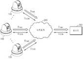
도 1은 본 발명의 일 실시 예에 따른 원격 FPGA 배열 변경 시스템을 개략적으로 나타낸 도면이다.
도 2는 본 발명의 일 실시 예에 따른 원격 FPGA 배열 변경 시스템이 사용되는 카메라를 나타내는 블록도이다.
도 3은 본 발명의 일 실시예에 따른 FPGA 보드의 내부 구성을 나타낸 도면이다.
도 4는 카메라의 용도에 따라 다른 ISP의 영상 처리 과정을 개략적으로 나타낸 도면이다.
도 5는 본 발명의 일 실시예에 따라 원격으로 FPGA 보드의 배열을 변경하는 방법을 나타내는 순서도이다.
도 6은 본 발명의 일 실시예에 따라 통신부를 갖는 FPGA 보드를 포함하는 카메라의 동작을 순서도로 나타낸 도면이다.1 is a schematic diagram of a remote FPGA array modification system in accordance with an embodiment of the present invention.
2 is a block diagram illustrating a camera in which a remote FPGA array modification system according to an embodiment of the invention is used.
3 is a diagram illustrating an internal configuration of an FPGA board according to an embodiment of the present invention.
4 is a diagram schematically illustrating an image processing procedure of another ISP according to the use of the camera.
5 is a flowchart illustrating a method of remotely changing the arrangement of FPGA boards according to an embodiment of the present invention.
6 is a flowchart illustrating an operation of a camera including an FPGA board having a communication unit according to an exemplary embodiment of the present invention.
후술하는 본 발명에 대한 상세한 설명은, 본 발명이 실시될 수 있는 특정 실시예를 예시로서 도시하는 첨부 도면을 참조한다. 이러한 실시예는 당업자가 본 발명을 실시할 수 있기에 충분하도록 상세히 설명된다. 본 발명의 다양한 실시예는 서로 다르지만 상호 배타적일 필요는 없음이 이해되어야 한다. 예를 들어, 본 명세서에 기재되어 있는 특정 형상, 구조 및 특성은 본 발명의 정신과 범위를 벗어나지 않으면서 일 실시예로부터 다른 실시예로 변경되어 구현될 수 있다. 또한, 각각의 실시예 내의 개별 구성요소의 위치 또는 배치도 본 발명의 정신과 범위를 벗어나지 않으면서 변경될 수 있음이 이해되어야 한다. 따라서, 후술하는 상세한 설명은 한정적인 의미로서 행하여지는 것이 아니며, 본 발명의 범위는 특허청구범위의 청구항들이 청구하는 범위 및 그와 균등한 모든 범위를 포괄하는 것으로 받아들여져야 한다. 도면에서 유사한 참조부호는 여러 측면에 걸쳐서 동일하거나 유사한 구성요소를 나타낸다.The following detailed description of the invention refers to the accompanying drawings, which illustrate, by way of illustration, specific embodiments in which the invention may be practiced. These embodiments are described in sufficient detail to enable those skilled in the art to practice the invention. It should be understood that the various embodiments of the present invention are different, but need not be mutually exclusive. For example, the specific shapes, structures, and characteristics described herein may be implemented by changing from one embodiment to another without departing from the spirit and scope of the invention. It should also be understood that the location or arrangement of individual components within each embodiment may be varied without departing from the spirit and scope of the present invention. Therefore, the following detailed description is not to be taken in a limiting sense, and the scope of the present invention should be construed as encompassing the scope of the appended claims and all equivalents thereof. In the drawings, like reference numbers designate the same or similar components throughout the several views.
이하에서는, 본 발명이 속하는 기술분야에서 통상의 지식을 가진 자가 본 발명을 용이하게 실시할 수 있도록 하기 위하여, 본 발명의 여러 실시예에 관하여 첨부된 도면을 참조하여 상세히 설명하기로 한다.DETAILED DESCRIPTION OF THE PREFERRED EMBODIMENTS Hereinafter, embodiments of the present invention will be described in detail with reference to the accompanying drawings in order to facilitate a person skilled in the art to which the present invention pertains.
도 1은 본 발명의 일 실시 예에 따른 원격 FPGA 배열 변경 시스템을 개략적으로 나타낸 도면이다.1 is a schematic diagram of a remote FPGA array modification system in accordance with an embodiment of the present invention.
도 1을 참조하면, 복수 개의 카메라들(100)이 네트워크(200)를 통해 호스트 장치(300)와 데이터를 주고받고 있다. 구체적으로, 카메라들(100)은 통신 채널(DCOM)을 통하여 호스트 장치(300)와 통신하면서, 영상 데이터 채널(DIMA)을 통하여 라이브 뷰 동영상 데이터를 호스트 장치(300)에 전달한다. 물론 복수 개의 카메라가 아닌 한 개의 카메라만 호스트 장치(300)와 통신할 수도 있고, 한 개의 카메라 또는 복수 개의 카메라들이 복수 개의 호스트 장치(300)들과 통신할 수도 있는 등 다양한 변형이 가능함은 물론이다. 여기서 통신 채널(DCOM) 및 영상 데이터 채널(DIMA)을 형성하는 네트워크(200)는 유선 또는 무선으로 데이터나 명령을 송수신할 수 있는 모든 수단이 될 수 있다. 예를 들어, 네트워크(200)는 케이블을 통하여 유선으로 카메라(100)와 호스트 장치(300)를 연결할 수도 있으며, 무선 랜 등을 사용하여 무선으로 카메라(100)와 호스트 장치(300)를 연결할 수도 있다. 바람직하게는, 네트워크(200)는 이더넷(ethernet) 네트워크와 같은 근거리 통신망(local area network)일 수 있다.Referring to FIG. 1, a plurality of
도 1에서는 호스트 장치(300)가 컴퓨터와 유사한 형태를 갖는 것으로 도시하고 있으나 본 실시 예에 따른 카메라(100)가 도 1에 도시된 것과 같은 호스트 장치(300)와만 통신할 수 있는 것은 아니며, 디스플레이 화면을 갖는 장치라면 어떠한 것이든 가능함은 물론이다. 예를 들어, 호스트 장치(300)로 개인용 컴퓨터 등이 사용될 수도 있을 것이다. 호스트 장치(300)는 필요에 따라 카메라(100)로부터의 라이브 뷰 동영상을 저장할 수도 있다.1, the
본 발명에서, 호스트 장치(300)는 카메라(100) 내부의 후술할 FPGA 보드(140)에 탑재된 이미지 신호 처리 장치(Image Signal Processor, 이하 'ISP'라 한다) 설정을 변경하기 위한 배열(configuration) 파일을 생성할 수 있다. 즉, 본 발명의 일 실시예에서 호스트 장치(300)는 네트워크(200)를 통해 원격으로 카메라(100)의 ISP 설정을 변경할 수 있다.In the present invention, the
도 2는 본 발명의 일 실시 예에 따른 원격 FPGA 배열 변경 시스템이 사용되는 카메라를 나타내는 블록도이다.2 is a block diagram illustrating a camera in which a remote FPGA array modification system according to an embodiment of the invention is used.
도 2를 참조하면, 본 실시 예에 따른 카메라(100)는, 렌즈부(110), 촬상소자(111), 촬상소자 제어부(112), 드라이버(113), 모터(114), 사전 처리부(120), 압축 신장부(121), ROM(131), RAM(132), 메모리 콘트롤러(133), 카메라 메모리(134), FPGA 보드(140), 카메라 디스플레이부(150), 카메라 통신부(160), 카메라 조작부(170) 등을 포함할 수 있다.2, the
렌즈부(110)는 외부의 광 정보를 촬상소자(111)에 결상시키는 광학계 시스템으로, 피사체로부터의 광을 촬상소자(111)까지 투과시킨다. 렌즈부(110)는 초점거리를 변화시키는 줌 렌즈, 초점을 조절하는 포커스 렌즈 등의 렌즈군과 투과하는 광량을 조절하는 조리개 등으로 이루어진다.The
렌즈부(110)에 포함되는 줌 렌즈, 조리개, 포커스 렌즈 등은 드라이버(113)로부터 구동신호를 인가받은 모터(114)에 의해 구동된다.The zoom lens, diaphragm, focus lens, and the like included in the
촬상소자(111)는 광전변환소자의 일례로서, 렌즈부(110)를 투과하여 입사된 영상광을 촬상하여 전기신호로 변환하는 광전 변환이 가능한 복수의 소자로 구성된다. 각 소자는 입사된 빛에 따른 전기신호를 생성하여 영상신호를 생성한다. 이때, 촬상소자(11)는 촬상소자 제어부(112)로부터의 타이밍 신호에 따라서 미리 설정된 주기로 프레임 영상을 촬상하여 영상신호를 주기적으로 생성한다. 촬상소자(111)는 CCD(charge coupled device) 센서, CMOS(complementary metal oxide semiconductor) 센서 등을 적용할 수 있다. 촬상소자(111)는 광전변환 및 Analog/Digital 변환에 의하여 생성한 디지털 신호를 사전 처리부(120)로 출력한다.The
촬상소자 제어부(112)는 타이밍 신호를 생성하고, 타이밍 신호에 동기하여 상기 촬상소자(111)가 촬상하도록 제어한다.The image pickup
사전 처리부(120)는 촬상소자(111)로부터 출력된 디지털 신호에 대해 처리를 하여 영상처리가 가능하게 되는 영상신호를 생성한다. 사전 처리부(120)는, 영상신호를 FPGA 보드(140)로 출력한다. 또한, 사전 처리부(120)는 RAM(132)으로의 영상 데이터의 읽기 및 쓰기를 제어한다.The
압축 신장부(121)는 압축 처리 전의 영상신호를 수신하여, 예를 들면 MPEG, ACI, MOV, ASD 등의 압축 형식으로 영상신호를 압축 처리한다. 압축 신장부(121)는 압축 처리로 생성한 영상 데이터를 포함하는 영상 파일을 메모리 콘트롤러(133)로 전송한다. 또는 압축 신장부(121)는 영상 파일을 카메라 통신부(160)에 입력하고, 카메라 통신부(160)를 통하여 카메라(110)를 제어하는 메인 서버(300) 등으로 전송할 수도 있다. 또한 압축 신장부(121)는 카메라 디스플레이부(150)를 구비하는 경우, 카메라 메모리(134)에 저장된 영상 파일을 추출한 후 신장 처리를 수행하여 카메라 디스플레이부(150)에서 재생될 수 있도록 한다.The compression /
ROM(read only memory, 131)은 촬영 조건 등과 관련된 사용자의 설정 데이터가 저장될 수 있다. 또한 ROM(131)은 FPGA(140)에서 카메라(100)를 제어하기 위하여 사용하는 알고리즘이 저장될 수 있다. 이러한 ROM(131)으로는 EEPROM(electrically erasable and programmable read only memory) 등이 사용될 수 있다.A ROM (read only memory) 131 may store user setting data related to shooting conditions and the like. Also, the
RAM(random access memory, 132)은 사전 처리부(120)에서 출력된 영상신호, FPGA 보드(140)에서 신호 처리 과정에서 생성되는 데이터 등, 각종 데이터를 일시적으로 저장하는 부분이다. RAM(132)으로 DRAM(dynamic RAM)을 사용할 수 있다.A random access memory (RAM) 132 is a part for temporarily storing various data such as a video signal output from the
메모리 컨트롤러(133)는 카메라 메모리(134)로의 영상 데이터의 기입, 또는 상기 카메라 메모리(134)에 기록된 영상 데이터나 설정 정보 등의 독출을 제어한다. 카메라 메모리(134)는, 예를 들면 광디스크(CD, DVD, 블루레이 디스크 등), 광자기 디스크, 자기 디스크, 반도체 기억 매체 등으로서, 촬영된 영상 데이터를 기록한다. 상기 영상 데이터는 압축 신장부(121)에서 생성된 영상 파일에 포함된 것일 수 있다. 메모리 콘트롤러(133), 카메라 메모리(134)는 카메라(100)로부터 착탈 가능하게 구성되어도 좋다. 그러나 메모리 콘트롤러(133) 및 카메라 메모리(134)는 카메라(100)에 반드시 설치되어야 하는 것은 아니며, 카메라(100)가 네트워크(200)를 통하여 메인 서버(300)에 연결된 카메라 등일 경우에는 카메라(100)를 제어하는 메인 서버(300) 측에 영상 데이터 등을 저장하기 위한 서버 메모리(350)가 구비될 수 있을 것이다. 이때, 영상 데이터 등은 카메라 통신부(160)에 의하여 네트워크(200)를 통하여 카메라(100)로부터 메인 서버(300)로 전송될 수 있을 것이다.The
다음으로, FPGA(field programmable gate array) 보드(140)는 본 발명의 일 실시예에서 카메라(100)에 내장되어 각종 카메라 설정을 저장 및 변경하고, ISP를 사용하여 영상 처리를 행하며, 호스트 장치(300)로부터 배열 정보를 다운받아 ISP를 변경 할 수 있다. 본 발명에서, 카메라(100)는 FPGA 보드(140)를 장착함으로써, 촬상 대상으로부터 얻은 이미지 데이터를 네트워크(200)를 통해 호스트 장치(300) 컴퓨터에서 처리하는 것이 아니라 후처리된 이미지를 호스트 장치(300)에 바로 전송할 수 있다.Next, a field programmable gate array (FPGA)
본 발명의 FPGA보드(140)는 카메라에 내장된 현장 프로그램가능 게이트 어레이로서, 프로그래머블 논리 요소와 프로그래밍가능 내부선이 포함된 반도체 소자를 말한다. 그리고, 프로그래머블 논리 요소는 AND, OR, XOR, NOT, 더 복잡한 디코더나 계산기능의 조합 기능 같은 기본적인 논리 게이트의 기능을 복재하여 프로그래밍할 수 있다. 또한, 본 발명의 FPGA 보드(140)는 프로그래밍가능 논리 요소에 간단한 플립플롭이나 더 완벽한 메모리 블록으로 된 메모리 요소도 포함할 수 있다. 이러한 논리블록과 내부선은 제조공정 이후에 프로그램, 즉 FPGA 보드(140)의 배열(configuration)을 새로이 기록하거나 변경할 수 있어서 필요로 되는 어떠한 논리기능이라도 수행할 수 있게 된다.The
특히, 본 발명의 일 실시예에 카메라(100)에 포함된 FPGA 보드(140)의 프로그램은 네트워크(200)를 통해 호스트 장치(300)에서 전송된 배열 정보를 통해 변경될 수 있다. 이에 의해, 카메라(100)는 생산 당시 설정되었던, 예를 들어 열상 카메라용 기능, 감시 카메라용 기능 등에 국한되지 않고 다양하게 그 용도를 변경할 수 있다. FPGA 보드(140) 내부의 상세한 구성에 대해서는 아래의 도 3에서 후술하기로 한다.In particular, the program of the
카메라 디스플레이부(150)는 촬영된 영상이나 촬영되어 카메라 메모리(134)에 저장된 영상, 또는 압축 신장부(121)에서 신장 처리된 영상 등을 표시한다. 또한 카메라 디스플레이부(150)는 카메라(100)의 제어를 위한 각종 설정 화면 등이 표시될 수 있다.The
카메라 통신부(160)는 카메라(100)에서 촬영된 라이브 뷰 영상이나 촬영되어 카메라 메모리(134)에 저장된 영상을 유선 또는 무선 네트워크(200)를 통하여 외부 장치, 예를 들어 호스트 장치(300)로 전송한다. 또한 카메라 통신부(160)는 네트워크(200)를 통하여 호스트 장치(300)로부터 전송되는 각종 명령 신호를 수신한다. 특히, 본 발명의 일 실시예에서 카메라 통신부(160)는 호스트 장치(300)로부터 FPGA 보드(140)의 배열 정보를 다운로드 할 수 있다.The
카메라 조작부(170)는, 예를 들면 카메라(100)에 설치된 각종 버튼이나 레버 등을 포함하며, 사용자에 의한 조작에 기초하여 조작신호를 FPGA 보드(140) 등에 전송한다. 그러나 카메라 조작부(170)는 카메라(100)에 반드시 설치되어야 하는 것은 아니며, 카메라(100)가 네트워크(200)로 연결된 카메라 등일 경우에는 카메라(100)를 제어하는 메인 서버(300) 측에 서버 조작부(330)를 구비하고, 이를 통하여 인가되는 신호를 통하여 카메라(100)의 동작을 제어할 수도 있을 것이다.The
도 3은 본 발명의 일 실시예에 따른 FPGA 보드의 내부 구성을 나타낸 도면이다.3 is a diagram illustrating an internal configuration of an FPGA board according to an embodiment of the present invention.
도 3을 참조하면, 본 발명의 FPGA 보드는 제어부(141), 통신부(142), 저장부(143), 영상 처리부(144)를 포함한다. 본 발명의 일 실시예에 따르면, FPGA 보드(140)는 배열 정보를 업데이트함으로써 원격으로 카메라(100)의 소프트웨어 뿐만 아니라 하드웨어 설정을 변경할 수 있으므로, 원격으로 FPGA 보드(140)의 배열을 변경하여 카메라의 영상 처리 방법, 즉 ISP의 설정을 변경할 수 있다.Referring to FIG. 3, the FPGA board of the present invention includes a
제어부(141)는, 프로그램에 의해 연산처리장치 및 제어장치로서 기능하고, 카메라(100) 내에 설치된 각 구성요소의 처리를 제어한다. 본 발명의 일 실시예에서, 제어부(141)는 제어 기능을 수행하는 하나 이상의 CPU 장치로 구성될 수 있다. 제어부(141)는, 예를 들면 포커스 제어나 노출 제어에 기초하여 드라이버(113)로 신호를 출력하여 모터(114)를 구동시킨다. 또한, 제어부(141)는 카메라 조작부(170)로부터의 신호에 기초하여 카메라(100)의 각 구성요소를 제어한다. 또, 본 실시 예에서는, 제어부(141)가 하나의 CPU로 이루어진 구성일 수 있고, 신호계의 명령과 조작계의 명령을 별도의 CPU에서 행하는 등 복수의 CPU로 구성되어도 된다.The
다음으로, 통신부(142)는 FPGA 보드(140)와 카메라(100) 내부의 다른 기기들간의 통신을 수행한다. 특히, 통신부(142)는 카메라 통신부(160)가 호스트 장치(300)로부터 수신한 배열 정보를 후술할 저장부(143)가 FPGA 보드에 적용할 수 있도록 전달하는 역할을 한다. 도 2 및 도 3에서는 비록 통신부(142)가 카메라 통신부(160)와는 별개로 FPGA 보드(140) 내에 내장된 것으로 표시되었지만, 본 발명의 다른 실시예에서는 통신부(142)가 카메라 통신부(160)의 역할까지 겸하여 직접 호스트 장치(300)와 네트워크(200)를 통해 통신할 수 있다. 또한, 본 발명의 일 실시예에서 통신부(142)는 FPGA 보드(140) 내에 내장된 이더넷 컨트롤러(ethernet controller)로서 기능할 수 있다.Next, the
다음으로, 저장부(143)는 통신부(142)가 호스트 장치(300)로부터 원격으로 수신한 ISP에 관련된 배열 정보를 FPGA 보드(140)에 기록하는 역할을 한다. 본 발명의 일 실시예에서, 저장부(143)는 FPAG 보드(140) 내의 SRAM(Static RAM)에 배열 정보를 저장할 수 있다. 본 발명에서 FPGA 보드(140)는 프로그래밍 하기 위한 연결 스위치 점이 SRAM 셀에 의해 조정되고 연결점을 제어하기 위한 배열 정보가 SRAM 셀에 저장된다. 이와 같은 SRAM은 휘발성(Volatile) 소자이므로 배열 정보는 전원이 꺼지면 그 정보가 유실되지만, 전원이 인가된 상태에서도 배열 정보를 기록할 수 있으므로 저장부(143)는 이러한 점을 활용하여 다운받은 배열 정보를 사용하여 FPGA 보드(140)의 ISP 기능을 저장 또는 변경할 수 있다.The
기존의 카메라에 내장된 ISP는 생산시 한번 적용되면 그 설정을 바꿀 수 없어 카메라의 용도를 변경하기 위해서는 카메라의 하드웨어를 교체해야 하는 불편함이 있었다. 이에 반해, 본 발명의 일 실시예에 따르면, 저장부(143)는 FPGA 보드(140) 내에 저장된 ISP를 네트워크(200)를 통해 전송된 배열 정보를 사용하여 업데이트할 수 있다. 따라서 카메라 하드웨어의 변경 없이도 원격으로 카메라(100) ISP를 변경할 수 있어 사용자의 편의성을 증가시킬 수 있다.The existing ISP's built-in ISP can not change its settings once it is applied to production, so it was inconvenient to change the camera's hardware in order to change the purpose of the camera. In contrast, according to an embodiment of the present invention, the
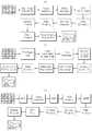
도 4는 카메라의 용도에 따라 서로 다른 ISP의 영상 처리 과정을 개략적으로 나타낸 도면이다.FIG. 4 is a diagram schematically illustrating an image processing process of different ISPs according to the use of the camera.
도 4의 (a), (b), (c)는 각각 다른 기능을 가진 ISP의 이미지 신호 처리 과정을 나타낸 블록도를 나타낸다. (a)는 범용 카메라의 ISP, (b)는 CCTV용 카메라의 ISP, (c)는 열상 카메라의 ISP이다.4 (a), 4 (b) and 4 (c) are block diagrams showing an image signal processing process of an ISP having different functions. (a) is an ISP of a general-purpose camera, (b) is an ISP of a CCTV camera, and (c) is an ISP of a thermal camera.
도 4의 (a)에서 볼 수 있는 바와 같이, 범용 카메라의 ISP는 Black Level Adjustment, Noise Reduction, White Balance, CFA Interpolation, Color Correction, Gamma Correction, Edge Enhance, Contrast Enhance, Color Enhance, False Chroma Suppression 과정을 통해 이미지를 처리한다. 각 과정의 구체적인 영상 처리 방법은 종래의 기술을 참조할 수 있다.As shown in (a) of FIG. 4, the ISP of the general-purpose camera performs various processes such as Black Level Adjustment, Noise Reduction, White Balance, CFA Interpolation, Color Correction, Gamma Correction, Edge Enhance, Contrast Enhance, Color Enhance, False Chroma Suppression To process the image. Conventional techniques can be referred to as specific image processing methods of each process.
다음으로, 도 4의 (b)에서 볼 수 있는 바와 같이 CCTV용 카메라의 ISP는 8Bit Bayer Data, Color Interpolation to 24bit RGB, Color Correction, RG Gain Control By AWB, Gamma Correction, Color Space Conversion, Histogram Equalization, Edge Enhance, YCbCr 4:2:2 Format output 과정을 통해 이미지를 처리한다. 마찬가지로, 각 과정의 구체적인 영상처리 방법은 종래의 기술을 참조할 수 있다.As shown in FIG. 4B, the ISP of the CCTV camera includes 8Bit Bayer Data, Color Interpolation to 24bit RGB, Color Correction, RG Gain Control By AWB, Gamma Correction, Color Space Conversion, Histogram Equalization, Edge enhancement, and YCbCr 4: 2: 2 format output. Likewise, a specific image processing method of each process can refer to conventional techniques.
마지막으로, 도 4의 (c)에서 볼 수 있는 바와 같이 열상 카메라의 ISP는 NUC, Defect Correction, DAE, VGA Controller, ANDR, Edge Enhance, Gamma Enhance, Contrast Enhance, OSD Font, ITU656 Encoder 과정을 통해 이미지를 처리한다. 마찬가지로, 각 과정의 구체적인 영상처리 방법은 종래의 기술을 참조할 수 있다.Finally, as shown in FIG. 4 (c), the ISP of the thermal camera transmits the image through the NUC, Defect Correction, DAE, VGA Controller, ANDR, Edge Enhance, Gamma Enhance, Contrast Enhance, OSD Font, . Likewise, a specific image processing method of each process can refer to conventional techniques.
도 4에서 볼 수 있는 바와 같이, 카메라의 용도에 따라 ISP는 차이가 있으며, 기존에는 서로 다른 ISP를 적용하기 위하여 카메라 하드웨어를 변경하는 작업이 필요했다. 이에 반해, 본 발명의 일 실시예에서는 원격으로 ISP의 설정을 포함하는 배열 정보를 호스트 장치(300)로부터 다운로드하여 FPGA 보드(140)에 기록할 수 있다. 즉, 도 4의 (a)와 같은 일반 카메라의 ISP가 FPGA 보드(140)에 적용되어 있는 경우에도, 저장부(143)는 호스트 장치(300)로부터 CCTV용 ISP를 적용한 배열 정보를 다운받아 FPGA 보드(140)에 업데이트함으로써 카메라의 ISP를 CCTV 용으로 변경할 수 있다.As can be seen from FIG. 4, ISPs differ according to the use of cameras, and in the past, it was necessary to change the camera hardware in order to apply different ISPs. In contrast, in one embodiment of the present invention, the array information including the setting of the ISP can be remotely downloaded from the
또한, 본 발명의 다른 실시예에서, 저장부(143)는 배열 정보를 다운로드하여 기존의 ISP에서 변경된 부분만을 FPGA 보드(140)에 기록할 수 있다. 예를 들어, 도 4의 (a)에서 점선으로 표시된 CFA Interpolation 등의 기능은 다른 용도의 ISP에서도 사용될 수 있다. 이 경우, 저장부(143)는 점선으로 표시된 공통 사용 기능은 제외하고 실선으로 표시된 변경 기능만을 타 ISP에 적용되는 기능으로 대체할 수 있다.Also, in another embodiment of the present invention, the
또한, 저장부(143)는 배열 정보를 영상 처리부(143)에 제공하기 전 배열 정보에 오류가 있는지 유무를 검사할 수 있다. 추가적으로, 저장부가 FPGA 보드(140)에 저장하는 배열 정보는 ISP에 관련된 것 뿐만이 아니라 카메라(100)의 유지 보수에 관련된 것일 수 있다. 예를 들어, FPAG 보드(140)의 특정 구성에 있어 오류가 있다고 감지되면, 호스트 장치(100)로부터 보수에 관한 배열 파일을 다운받아 FPGA 보드(140)의 배열을 변경할 수 있다.In addition, the
다음으로, 영상 처리부(144)는 사전 처리부(120)로부터 영상 신호를 받아 FPGA 보드(140)에 기록된 ISP를 토대로 영상을 처리한다. 보다 구체적으로, 영상 처리부(144)는 WB 제어값, γ값, 윤곽 강조 제어값 등에 기초하여 영상 처리된 영상신호를 생성한다. 영상 처리된 영상신호는 압축 신장부(121)에 인가될 수 있다. 영상 처리부(144)는 상술한 바와 같이 ISP의 종류에 따라 서로 다른 방법으로 영상을 처리한다. 추가적으로, 영상 처리된 영상신호는 라이브 뷰 영상으로 사용될 수 있으며, RAM(132)을 거쳐서 카메라 디스플레이부(150)로 전송될 수도 있다.Next, the
도 5는 본 발명의 일 실시예에 따라 원격으로 FPGA 보드의 배열을 변경하는 방법을 나타내는 순서도이다.5 is a flowchart illustrating a method of remotely changing the arrangement of FPGA boards according to an embodiment of the present invention.
먼저, 호스트는 카메라의 ISP에 관련된 FPGA 보드의 배열 정보를 생성한다(S11).First, the host generates array information of the FPGA board related to the ISP of the camera (S11).
다음으로, 카메라 내의 FPGA 보드는 생성된 배열 정보를 호스트로부터 네트워크를 통해 수신한다(S12).Next, the FPGA board in the camera receives the generated array information from the host through the network (S12).
다음으로, 배열 정보를 수신한 FPGA 보드는 배열 정보가 올바른지 여부를 검사한다(S13).Next, the FPGA board receiving the array information checks whether the array information is correct (S13).
다음으로, 수신한 배열 정보를 FPGA 보드에 업데이트하여 카메라의 ISP를 변경한다(S14).Next, the received array information is updated on the FPGA board to change the ISP of the camera (S14).
마지막으로, 변경된 ISP를 사용하여 이미지 센서가 얻은 영상을 처리한다(S15).Finally, the image obtained by the image sensor is processed using the changed ISP (S15).
도 6은 본 발명의 일 실시예에 따라 통신부를 갖는 FPGA 보드를 포함하는 카메라의 동작을 순서도로 나타낸 도면이다.6 is a flowchart illustrating an operation of a camera including an FPGA board having a communication unit according to an exemplary embodiment of the present invention.
먼저, 도 6을 참조하면, 카메라의 FPGA 보드는 이미지 센서의 이미지 센서의 드라이버에 클락(clock)을 공급한다(S21).First, referring to FIG. 6, the FPGA board of the camera supplies a clock to the driver of the image sensor of the image sensor (S21).
다음으로, 이미지 센서는 촬상된 이미지 데이터를 FPGA 보드에 저장한다(S22).Next, the image sensor stores the captured image data on the FPGA board (S22).
이 과정에서, FPGA 보드에 이상이 있는지를 점검하여(S23), 호스트 장치로부터 FPGA 보드의 유지 또는 보수를 위한 배열 정보를 전송받아 FPGA 보드에 저장할 수 있다(S24).In this process, it is checked whether there is an abnormality in the FPGA board (S23), and arrangement information for maintenance or repair of the FPGA board is received from the host device and stored in the FPGA board (S24).
다음으로, FPGA 보드의 ISP를 변경하고자 하는 경우, ISP에 관련된 생성된 배열 정보를 네트워크를 통해 수신한다(S25).Next, when it is desired to change the ISP of the FPGA board, the generated array information related to the ISP is received through the network (S25).
다음으로, 수신한 배열 정보를 FPGA 보드에 업데이트하여 카메라의 ISP를 변경한다(S26).Next, the received array information is updated on the FPGA board to change the ISP of the camera (S26).
마지막으로, ISP를 사용하여 영상 처리한 촬상 영상을 카메라 디스플레이에 제공하거나 네트워크를 통해 호스트 장치에 제공한다(S27).Finally, the captured image obtained by image processing using the ISP is provided to the camera display or provided to the host apparatus via the network (S27).
이상에서 본 발명이 구체적인 구성요소 등과 같은 특정 사항과 한정된 실시예 및 도면에 의하여 설명되었으나, 이는 본 발명의 보다 전반적인 이해를 돕기 위하여 제공된 것일 뿐, 본 발명이 상기 실시예에 한정되는 것은 아니며, 본 발명이 속하는 기술분야에서 통상적인 지식을 가진 자라면 이러한 기재로부터 다양한 수정과 변경을 꾀할 수 있다.While the present invention has been particularly shown and described with reference to exemplary embodiments thereof, it is to be understood that the invention is not limited to the disclosed embodiments, but, on the contrary, Those skilled in the art will appreciate that various modifications and changes may be made thereto without departing from the scope of the present invention.
따라서, 본 발명의 사상은 상기 설명된 실시예에 국한되어 정해져서는 아니 되며, 후술하는 특허청구범위뿐만 아니라 이 특허청구범위와 균등한 또는 이로부터 등가적으로 변경된 모든 범위는 본 발명의 사상의 범주에 속한다고 할 것이다.Accordingly, the spirit of the present invention should not be construed as being limited to the above-described embodiments, and all ranges that are equivalent to or equivalent to the claims of the present invention as well as the claims .
100감시 카메라200네트워크
300호스트 장치111렌즈부
111촬상소자112촬상소자 제어부
113드라이버114모터
120사전 처리부121압축 신장부
131ROM132RAM
133메모리 컨트롤러134카메라 메모리
140FPGA 보드141제어부
142통신부143저장부
144영상 처리부150카메라 디스플레이부
160카메라 통신부170카메라 조작부100
300
113
120
131
133
140
142
144
160
Claims (20)
Translated fromKorean상기 FPGA 보드에 상기 배열 정보를 기록하는 저장부; 및
상기 FPGA 보드에 기록된 상기 배열 정보를 이용하여 영상 처리를 행하는 영상 처리부;를 포함하고,
상기 저장부는 상기 배열 정보와 상기 FPGA 보드에 저장된 기존의 배열 정보를 비교하여, 상기 기존의 배열 정보에서 변경된 부분만 기록하는 것을 특징으로 하는 원격 FPGA 배열 변경 시스템.A communication unit for remotely receiving arrangement information of an FPGA board built in a camera;
A storage unit for storing the arrangement information on the FPGA board; And
And an image processor for performing image processing using the arrangement information recorded on the FPGA board,
Wherein the storage unit compares the array information with existing array information stored in the FPGA board and records only the changed part in the existing array information.
상기 배열 정보는 상기 카메라의 ISP(Image Signal Processor) 정보를 포함하는 것을 특징으로 하는 원격 FPGA 배열 변경 시스템.The method according to claim 1,
Wherein the arrangement information includes information of an ISP (Image Signal Processor) of the camera.
상기 카메라는, 범용 카메라이고,
상기 배열 정보는, Black Level Adjustment, Noise Reduction, White Balance, CFA Interpolation, Color Correction, Gamma Correction, Edge Enhance, Contrast Enhance, Color Enhance, 및 False Chroma Suppression 과정을 통해 이미지를 처리하는 상기 범용 카메라의 ISP 정보를 포함하고,
상기 기존의 배열 정보에서 변경된 부분은, 상기 Black Level Adjustment, 상기 Noise Reduction, 상기 White Balance, 상기 Color Enhance, 및 상기 False Chroma Suppression 과정 중 적어도 하나의 과정을 통해 이미지를 처리하는 ISP 정보인, 원격 FPGA 배열 변경 시스템.The method according to claim 1,
The camera is a general purpose camera,
The arrangement information may include at least one of ISP information of the general purpose camera for processing an image through a Black Level Adjustment, Noise Reduction, White Balance, CFA Interpolation, Color Correction, Gamma Correction, Edge Enhance, Contrast Enhance, Color Enhance, Lt; / RTI >
The changed part of the existing arrangement information may be the ISP information for processing the image through at least one of the Black Level Adjustment, the Noise Reduction, the White Balance, the Color Enhance, and the False Chroma Suppression process. Array Change System.
상기 배열 정보는 상기 카메라의 유지 보수 정보를 포함하는 것을 특징으로 하는 원격 FPGA 배열 변경 시스템.The method according to claim 1,
Wherein the arrangement information includes maintenance information of the camera.
상기 배열 정보를 상기 저장부에 기록하기 전 상기 배열 정보의 오류를 검사하는 것을 특징으로 하는 원격 FPGA 배열 변경 시스템.The method according to claim 1,
And an error of the array information is checked before writing the array information in the storage unit.
상기 ISP 정보는 이더넷(ethernet network)를 통해 수신하는 것을 특징으로 하는 원격 FPGA 배열 변경 시스템.3. The method of claim 2,
Wherein the ISP information is received via an Ethernet network.
상기 카메라는, CCTV용 카메라이고,
상기 배열 정보는, 8Bit Bayer Data, Color Interpolation to 24bit RGB, Color Correction, RG Gain Control By AWB, Gamma Correction, Color Space Conversion, Histogram Equalization, Edge Enhance, 및 YCbCr 4:2:2 Format output 과정을 통해 이미지를 처리하는 상기 CCTV용 카메라의 ISP 정보를 포함하고,
상기 기존의 배열 정보에서 변경된 부분은, 상기 8Bit Bayer Data, 상기 RG Gain Control By AWB, 상기 Color Space Conversion, 상기 Histogram Equalization, 및 상기 YCbCr 4:2:2 Format output 과정 중 적어도 하나의 과정을 통해 이미지를 처리하는 ISP 정보인, 원격 FPGA 배열 변경 시스템.The method according to claim 1,
The camera is a CCTV camera,
The arrangement information is obtained through the process of 8Bit Bayer Data, Color Interpolation to 24bit RGB, Color Correction, RG Gain Control By AWB, Gamma Correction, Color Space Conversion, Histogram Equalization, Edge Enhance, and YCbCr 4: The ISP information of the CCTV camera,
The modified part of the existing arrangement information may include at least one of the 8Bit Bayer Data, the RG Gain Control By AWB, the Color Space Conversion, the Histogram Equalization, and the YCbCr 4: 2: The remote FPGA array changing system comprising:
상기 카메라는, 열상 카메라이고,
상기 배열 정보는, NUC, Defect Correction, DAE, VGA Controller, ANDR, Edge Enhance, Gamma Enhance, Contrast Enhance, OSD Font, ITU656 Encoder 과정을 통해 이미지를 처리하는 상기 열상 카메라의 ISP 정보를 포함하고,
상기 기존의 배열 정보에서 변경된 부분은, 상기 NUC, 상기 Defect Correction, 상기 DAE, 상기 VGA Controller, 상기 ANDR, 상기 OSD Font, 상기 ITU656 Encoder 과정 중 적어도 하나의 과정을 통해 이미지를 처리하는 ISP 정보인, 원격 FPGA 배열 변경 시스템.The method according to claim 1,
The camera is a thermal camera,
The arrangement information includes ISP information of the thermal imaging camera that processes an image through NUC, Defect Correction, DAE, VGA Controller, ANDR, Edge Enhance, Gamma Enhance, Contrast Enhance, OSD Font,
Wherein the changed portion of the existing arrangement information is ISP information for processing an image through at least one of NUC, the Defect Correction, the DAE, the VGA Controller, the ANDR, the OSD Font, and the ITU656 Encoder process. Remote FPGA Array Change System.
상기 FPGA 보드의 ISP(Image Signal Processor)를 변경하고자 하는 경우, 상기 ISP에 관련된 생성된 상기 배열 정보를 네트워크를 통해 수신하는 단계;
수신한 상기 배열 정보를 상기 FPGA 보드에 업데이트하는 단계;
상기 FPGA 보드를 사용하여 영상 처리를 행하는 단계;
를 포함하고,
상기 업데이트하는 단계는, 상기 배열 정보와 상기 FPGA 보드에 저장된 기존의 배열 정보를 비교하여, 상기 기존의 배열 정보에서 변경된 부분만 기록하는 것을 특징으로 하는 카메라 제어 방법.Generating array information of an FPGA board embedded in a camera;
Receiving, through a network, the generated arrangement information related to the ISP when the ISP (Image Signal Processor) of the FPGA board is changed;
Updating the received array information to the FPGA board;
Performing image processing using the FPGA board;
Lt; / RTI >
Wherein the updating step compares the arrangement information with existing arrangement information stored in the FPGA board and records only the changed part in the existing arrangement information.
상기 배열 정보는 상기 카메라의 유지 보수에 관련된 정보를 포함하는 것을 특징으로 하는 카메라 제어 방법.20. The method of claim 19,
Wherein the arrangement information includes information related to maintenance of the camera.
Priority Applications (2)
| Application Number | Priority Date | Filing Date | Title |
|---|---|---|---|
| KR1020120054446AKR101695251B1 (en) | 2012-05-22 | 2012-05-22 | System for reconfiguring fpga remotely and method for controlling camera |
| US13/898,853US9077887B2 (en) | 2012-05-22 | 2013-05-21 | Camera having reconfigurable logic blocks in integrated circuit embedded thereon and system having the camera |
Applications Claiming Priority (1)
| Application Number | Priority Date | Filing Date | Title |
|---|---|---|---|
| KR1020120054446AKR101695251B1 (en) | 2012-05-22 | 2012-05-22 | System for reconfiguring fpga remotely and method for controlling camera |
Publications (2)
| Publication Number | Publication Date |
|---|---|
| KR20130130545A KR20130130545A (en) | 2013-12-02 |
| KR101695251B1true KR101695251B1 (en) | 2017-01-12 |
Family
ID=49621305
Family Applications (1)
| Application Number | Title | Priority Date | Filing Date |
|---|---|---|---|
| KR1020120054446AActiveKR101695251B1 (en) | 2012-05-22 | 2012-05-22 | System for reconfiguring fpga remotely and method for controlling camera |
Country Status (2)
| Country | Link |
|---|---|
| US (1) | US9077887B2 (en) |
| KR (1) | KR101695251B1 (en) |
Families Citing this family (16)
| Publication number | Priority date | Publication date | Assignee | Title |
|---|---|---|---|---|
| US10270709B2 (en) | 2015-06-26 | 2019-04-23 | Microsoft Technology Licensing, Llc | Allocating acceleration component functionality for supporting services |
| DE102014208771A1 (en)* | 2014-05-09 | 2015-11-12 | Mobotix Ag | Dynamically configured video camera |
| US10511478B2 (en) | 2015-04-17 | 2019-12-17 | Microsoft Technology Licensing, Llc | Changing between different roles at acceleration components |
| US10198294B2 (en) | 2015-04-17 | 2019-02-05 | Microsoft Licensing Technology, LLC | Handling tenant requests in a system that uses hardware acceleration components |
| US9792154B2 (en) | 2015-04-17 | 2017-10-17 | Microsoft Technology Licensing, Llc | Data processing system having a hardware acceleration plane and a software plane |
| US10296392B2 (en) | 2015-04-17 | 2019-05-21 | Microsoft Technology Licensing, Llc | Implementing a multi-component service using plural hardware acceleration components |
| US10516865B2 (en) | 2015-05-17 | 2019-12-24 | Endochoice, Inc. | Endoscopic image enhancement using contrast limited adaptive histogram equalization (CLAHE) implemented in a processor |
| KR102105093B1 (en) | 2015-06-08 | 2020-04-28 | 배틀카트 유럽 | Environment creation system |
| US9819542B2 (en) | 2015-06-26 | 2017-11-14 | Microsoft Technology Licensing, Llc | Configuring acceleration components over a network |
| US10216555B2 (en) | 2015-06-26 | 2019-02-26 | Microsoft Technology Licensing, Llc | Partially reconfiguring acceleration components |
| US10165180B2 (en)* | 2016-08-26 | 2018-12-25 | Cisco Technology, Inc. | Dynamic deployment of executable recognition resources in distributed camera devices |
| DE102017204463A1 (en)* | 2017-03-17 | 2018-09-20 | Sirona Dental Systems Gmbh | Color reference for calibrating a dental color camera |
| CN108810395B (en)* | 2017-05-05 | 2020-11-06 | 瑞芯微电子股份有限公司 | A method and device for rapidly displaying initial frame images and rapidly capturing images |
| TWI685786B (en)* | 2018-10-25 | 2020-02-21 | 神雲科技股份有限公司 | Firmware updating method for fpga |
| JP2022133135A (en)* | 2021-03-01 | 2022-09-13 | キヤノン株式会社 | IMAGING DEVICE, CONTROL METHOD OF IMAGING DEVICE, INFORMATION PROCESSING DEVICE |
| US12158849B2 (en)* | 2021-12-17 | 2024-12-03 | Dspace Gmbh | Method for data communication between subregions of an FPGA |
Family Cites Families (11)
| Publication number | Priority date | Publication date | Assignee | Title |
|---|---|---|---|---|
| KR100288561B1 (en)* | 1997-08-08 | 2001-05-02 | 윤종용 | Program Patching Method of Job Scheduler Software |
| JP4153522B2 (en)* | 2003-07-11 | 2008-09-24 | 株式会社日立製作所 | Image processing camera system and image processing camera control method |
| KR100669511B1 (en)* | 2005-01-31 | 2007-01-15 | 뷰웨이 주식회사 | Smart network camera |
| KR20070067306A (en)* | 2005-12-23 | 2007-06-28 | 엘지노텔 주식회사 | FPM programming device using IPC and its method |
| EP1809025A3 (en)* | 2006-01-17 | 2007-08-15 | STMicroelectronics (Research & Development) Limited | Memory enhanced image sensor |
| US7843487B2 (en) | 2006-08-28 | 2010-11-30 | Panasonic Corporation | System of linkable cameras, each receiving, contributing to the encoding of, and transmitting an image |
| US8542315B2 (en)* | 2007-11-27 | 2013-09-24 | Broadcom Corporation | Method and apparatus for expanded dynamic range imaging |
| KR100962987B1 (en) | 2008-07-18 | 2010-06-09 | 성균관대학교산학협력단 | Camera-attached image processing and data transmission device for optical motion capture |
| KR100972360B1 (en) | 2008-08-08 | 2010-07-26 | 뷰-하이텍주식회사 | Omnidirectional security camera system |
| FR2935078B1 (en) | 2008-08-12 | 2012-11-16 | Groupe Des Ecoles De Telecommunications Get Ecole Nationale Superieure Des Telecommunications Enst | METHOD OF PROTECTING THE DECRYPTION OF CONFIGURATION FILES OF PROGRAMMABLE LOGIC CIRCUITS AND CIRCUIT USING THE METHOD |
| KR101200433B1 (en)* | 2010-11-10 | 2012-11-22 | (주)아이아이에스티 | System for realtime observing fire using CCTV camera, and method for the same |
- 2012
- 2012-05-22KRKR1020120054446Apatent/KR101695251B1/enactiveActive
- 2013
- 2013-05-21USUS13/898,853patent/US9077887B2/enactiveActive
Also Published As
| Publication number | Publication date |
|---|---|
| US9077887B2 (en) | 2015-07-07 |
| US20130314559A1 (en) | 2013-11-28 |
| KR20130130545A (en) | 2013-12-02 |
Similar Documents
| Publication | Publication Date | Title |
|---|---|---|
| KR101695251B1 (en) | System for reconfiguring fpga remotely and method for controlling camera | |
| JP4943721B2 (en) | Color noise removal method for image data and imaging apparatus using the method | |
| US9538085B2 (en) | Method of providing panoramic image and imaging device thereof | |
| WO2008053716A1 (en) | Imaging device and imaging method | |
| US20140146185A1 (en) | Method and system for generating real-time motion video | |
| US8497922B2 (en) | Image processing apparatus and image processing method | |
| JP6300529B2 (en) | Imaging apparatus, control method therefor, program, and storage medium | |
| KR101747219B1 (en) | Camera and camera controlling method for generating privacy mask | |
| KR102229152B1 (en) | Image photographing appratus | |
| JP5084366B2 (en) | IMAGING DEVICE AND IMAGING DEVICE CONTROL METHOD | |
| JP2012114611A (en) | Imaging apparatus, image processing method, and program | |
| US20180197282A1 (en) | Method and device for producing a digital image | |
| US11622175B2 (en) | Electronic apparatus and control method thereof | |
| JP4343657B2 (en) | Image recording device | |
| JP2007274504A (en) | Digital camera | |
| JP5410158B2 (en) | Imaging system and electronic information device | |
| JP6083959B2 (en) | Transmission apparatus, control method thereof, and control program | |
| US20140168472A1 (en) | Image pickup device | |
| JP6083968B2 (en) | IMAGING DEVICE AND IMAGING DEVICE CONTROL METHOD | |
| US11616907B2 (en) | Image capturing apparatus, image capturing system, control method therefor, and storage medium | |
| KR101204093B1 (en) | Image processing apparatus and controlling method of the same | |
| JP6467455B2 (en) | IMAGING DEVICE, ITS CONTROL METHOD, PROGRAM, AND RECORDING MEDIUM | |
| JP4529782B2 (en) | Imaging apparatus and signal processing method thereof | |
| JP2006148456A (en) | Electronic camera | |
| KR101247320B1 (en) | Photographing apparatus |
Legal Events
| Date | Code | Title | Description |
|---|---|---|---|
| PA0109 | Patent application | Patent event code:PA01091R01D Comment text:Patent Application Patent event date:20120522 | |
| PG1501 | Laying open of application | ||
| A201 | Request for examination | ||
| PA0201 | Request for examination | Patent event code:PA02012R01D Patent event date:20151007 Comment text:Request for Examination of Application Patent event code:PA02011R01I Patent event date:20120522 Comment text:Patent Application | |
| E902 | Notification of reason for refusal | ||
| PE0902 | Notice of grounds for rejection | Comment text:Notification of reason for refusal Patent event date:20160817 Patent event code:PE09021S01D | |
| E701 | Decision to grant or registration of patent right | ||
| PE0701 | Decision of registration | Patent event code:PE07011S01D Comment text:Decision to Grant Registration Patent event date:20161201 | |
| GRNT | Written decision to grant | ||
| PR0701 | Registration of establishment | Comment text:Registration of Establishment Patent event date:20170105 Patent event code:PR07011E01D | |
| PR1002 | Payment of registration fee | Payment date:20170106 End annual number:3 Start annual number:1 | |
| PG1601 | Publication of registration | ||
| FPAY | Annual fee payment | Payment date:20191223 Year of fee payment:4 | |
| PR1001 | Payment of annual fee | Payment date:20191223 Start annual number:4 End annual number:4 | |
| PR1001 | Payment of annual fee | Payment date:20201228 Start annual number:5 End annual number:5 | |
| PR1001 | Payment of annual fee | Payment date:20211228 Start annual number:6 End annual number:6 | |
| PR1001 | Payment of annual fee | Payment date:20231220 Start annual number:8 End annual number:8 | |
| PR1001 | Payment of annual fee | Payment date:20241224 Start annual number:9 End annual number:9 |