KR101692799B1 - Wiring board and mounting structure thereof - Google Patents
Wiring board and mounting structure thereofDownload PDFInfo
- Publication number
- KR101692799B1 KR101692799B1KR1020110122845AKR20110122845AKR101692799B1KR 101692799 B1KR101692799 B1KR 101692799B1KR 1020110122845 AKR1020110122845 AKR 1020110122845AKR 20110122845 AKR20110122845 AKR 20110122845AKR 101692799 B1KR101692799 B1KR 101692799B1
- Authority
- KR
- South Korea
- Prior art keywords
- resin
- hole
- layer
- fiber layer
- concave portion
- Prior art date
- Legal status (The legal status is an assumption and is not a legal conclusion. Google has not performed a legal analysis and makes no representation as to the accuracy of the status listed.)
- Active
Links
Images

Classifications
- H—ELECTRICITY
- H05—ELECTRIC TECHNIQUES NOT OTHERWISE PROVIDED FOR
- H05K—PRINTED CIRCUITS; CASINGS OR CONSTRUCTIONAL DETAILS OF ELECTRIC APPARATUS; MANUFACTURE OF ASSEMBLAGES OF ELECTRICAL COMPONENTS
- H05K1/00—Printed circuits
- H05K1/02—Details
- H05K1/03—Use of materials for the substrate
- H05K1/0313—Organic insulating material
- H05K1/0353—Organic insulating material consisting of two or more materials, e.g. two or more polymers, polymer + filler, + reinforcement
- H05K1/0366—Organic insulating material consisting of two or more materials, e.g. two or more polymers, polymer + filler, + reinforcement reinforced, e.g. by fibres, fabrics
- H—ELECTRICITY
- H05—ELECTRIC TECHNIQUES NOT OTHERWISE PROVIDED FOR
- H05K—PRINTED CIRCUITS; CASINGS OR CONSTRUCTIONAL DETAILS OF ELECTRIC APPARATUS; MANUFACTURE OF ASSEMBLAGES OF ELECTRICAL COMPONENTS
- H05K3/00—Apparatus or processes for manufacturing printed circuits
- H05K3/40—Forming printed elements for providing electric connections to or between printed circuits
- H05K3/42—Plated through-holes or plated via connections
- H05K3/422—Plated through-holes or plated via connections characterised by electroless plating method; pretreatment therefor
- H—ELECTRICITY
- H05—ELECTRIC TECHNIQUES NOT OTHERWISE PROVIDED FOR
- H05K—PRINTED CIRCUITS; CASINGS OR CONSTRUCTIONAL DETAILS OF ELECTRIC APPARATUS; MANUFACTURE OF ASSEMBLAGES OF ELECTRICAL COMPONENTS
- H05K1/00—Printed circuits
- H05K1/02—Details
- H05K1/11—Printed elements for providing electric connections to or between printed circuits
- H05K1/115—Via connections; Lands around holes or via connections
- H05K1/116—Lands, clearance holes or other lay-out details concerning the surrounding of a via
- H—ELECTRICITY
- H05—ELECTRIC TECHNIQUES NOT OTHERWISE PROVIDED FOR
- H05K—PRINTED CIRCUITS; CASINGS OR CONSTRUCTIONAL DETAILS OF ELECTRIC APPARATUS; MANUFACTURE OF ASSEMBLAGES OF ELECTRICAL COMPONENTS
- H05K3/00—Apparatus or processes for manufacturing printed circuits
- H05K3/40—Forming printed elements for providing electric connections to or between printed circuits
- H05K3/42—Plated through-holes or plated via connections
- H—ELECTRICITY
- H10—SEMICONDUCTOR DEVICES; ELECTRIC SOLID-STATE DEVICES NOT OTHERWISE PROVIDED FOR
- H10D—INORGANIC ELECTRIC SEMICONDUCTOR DEVICES
- H10D64/00—Electrodes of devices having potential barriers
- H10D64/20—Electrodes characterised by their shapes, relative sizes or dispositions
- H10D64/23—Electrodes carrying the current to be rectified, amplified, oscillated or switched, e.g. sources, drains, anodes or cathodes
- H10D64/251—Source or drain electrodes for field-effect devices
- H10D64/254—Source or drain electrodes for field-effect devices for lateral devices wherein the source or drain electrodes extend entirely through the semiconductor bodies, e.g. via-holes for back side contacts
- H—ELECTRICITY
- H01—ELECTRIC ELEMENTS
- H01L—SEMICONDUCTOR DEVICES NOT COVERED BY CLASS H10
- H01L2224/00—Indexing scheme for arrangements for connecting or disconnecting semiconductor or solid-state bodies and methods related thereto as covered by H01L24/00
- H01L2224/01—Means for bonding being attached to, or being formed on, the surface to be connected, e.g. chip-to-package, die-attach, "first-level" interconnects; Manufacturing methods related thereto
- H01L2224/10—Bump connectors; Manufacturing methods related thereto
- H01L2224/15—Structure, shape, material or disposition of the bump connectors after the connecting process
- H01L2224/16—Structure, shape, material or disposition of the bump connectors after the connecting process of an individual bump connector
- H01L2224/161—Disposition
- H01L2224/16151—Disposition the bump connector connecting between a semiconductor or solid-state body and an item not being a semiconductor or solid-state body, e.g. chip-to-substrate, chip-to-passive
- H01L2224/16221—Disposition the bump connector connecting between a semiconductor or solid-state body and an item not being a semiconductor or solid-state body, e.g. chip-to-substrate, chip-to-passive the body and the item being stacked
- H01L2224/16225—Disposition the bump connector connecting between a semiconductor or solid-state body and an item not being a semiconductor or solid-state body, e.g. chip-to-substrate, chip-to-passive the body and the item being stacked the item being non-metallic, e.g. insulating substrate with or without metallisation
- H—ELECTRICITY
- H02—GENERATION; CONVERSION OR DISTRIBUTION OF ELECTRIC POWER
- H02K—DYNAMO-ELECTRIC MACHINES
- H02K2203/00—Specific aspects not provided for in the other groups of this subclass relating to the windings
- H02K2203/03—Machines characterised by the wiring boards, i.e. printed circuit boards or similar structures for connecting the winding terminations
- H—ELECTRICITY
- H05—ELECTRIC TECHNIQUES NOT OTHERWISE PROVIDED FOR
- H05K—PRINTED CIRCUITS; CASINGS OR CONSTRUCTIONAL DETAILS OF ELECTRIC APPARATUS; MANUFACTURE OF ASSEMBLAGES OF ELECTRICAL COMPONENTS
- H05K1/00—Printed circuits
- H05K1/02—Details
- H05K1/03—Use of materials for the substrate
- H05K1/0313—Organic insulating material
- H05K1/0353—Organic insulating material consisting of two or more materials, e.g. two or more polymers, polymer + filler, + reinforcement
- H05K1/0373—Organic insulating material consisting of two or more materials, e.g. two or more polymers, polymer + filler, + reinforcement containing additives, e.g. fillers
- H—ELECTRICITY
- H05—ELECTRIC TECHNIQUES NOT OTHERWISE PROVIDED FOR
- H05K—PRINTED CIRCUITS; CASINGS OR CONSTRUCTIONAL DETAILS OF ELECTRIC APPARATUS; MANUFACTURE OF ASSEMBLAGES OF ELECTRICAL COMPONENTS
- H05K1/00—Printed circuits
- H05K1/02—Details
- H05K1/11—Printed elements for providing electric connections to or between printed circuits
- H05K1/111—Pads for surface mounting, e.g. lay-out
- H05K1/112—Pads for surface mounting, e.g. lay-out directly combined with via connections
- H05K1/113—Via provided in pad; Pad over filled via
- H—ELECTRICITY
- H05—ELECTRIC TECHNIQUES NOT OTHERWISE PROVIDED FOR
- H05K—PRINTED CIRCUITS; CASINGS OR CONSTRUCTIONAL DETAILS OF ELECTRIC APPARATUS; MANUFACTURE OF ASSEMBLAGES OF ELECTRICAL COMPONENTS
- H05K2201/00—Indexing scheme relating to printed circuits covered by H05K1/00
- H05K2201/02—Fillers; Particles; Fibers; Reinforcement materials
- H05K2201/0203—Fillers and particles
- H05K2201/0206—Materials
- H05K2201/0209—Inorganic, non-metallic particles
- H—ELECTRICITY
- H05—ELECTRIC TECHNIQUES NOT OTHERWISE PROVIDED FOR
- H05K—PRINTED CIRCUITS; CASINGS OR CONSTRUCTIONAL DETAILS OF ELECTRIC APPARATUS; MANUFACTURE OF ASSEMBLAGES OF ELECTRICAL COMPONENTS
- H05K2201/00—Indexing scheme relating to printed circuits covered by H05K1/00
- H05K2201/09—Shape and layout
- H05K2201/09209—Shape and layout details of conductors
- H05K2201/095—Conductive through-holes or vias
- H05K2201/0959—Plated through-holes or plated blind vias filled with insulating material
Landscapes
- Engineering & Computer Science (AREA)
- Microelectronics & Electronic Packaging (AREA)
- Manufacturing & Machinery (AREA)
- Production Of Multi-Layered Print Wiring Board (AREA)
- Printing Elements For Providing Electric Connections Between Printed Circuits (AREA)
Abstract
Translated fromKoreanDescription
Translated fromKorean본 발명은 전자 기기(예를 들면 각종 오디오비주얼 기기, 가전 기기, 통신 기기, 컴퓨터 기기 및 그 주변 기기) 등에 사용되는 배선 기판 및 그 실장 구조체에 관한 것이다.BACKGROUND OF THE
종래, 전자 기기에 있어서의 실장 구조체로서는 배선 기판에 전자부품을 실장한 것이 사용되고 있다.2. Description of the Related Art Conventionally, as a mounting structure in an electronic apparatus, an electronic component is mounted on a wiring board.
배선 기판에 관해서 특허문헌 1에는 절연성 골재 및 수지 조성물로 이루어지는 절연층과, 상기 절연층을 두께방향으로 관통하는 관통 구멍과, 상기 관통 구멍 내에 형성된 도체층을 구비하고, 절연성 골재의 일부가 관통 구멍의 내벽으로부터 돌출된 구성이 개시되어 있다.
그런데, 인접하는 관통 구멍간에 전계가 인가되면 절연층에 포함되는 수분에 기인해서 도체층에 포함되는 도전재료가 이온화되어 인접하는 관통 구멍의 도체층을 향해서 절연층에 침입하는 경우가 있다(이온 마이그레이션).However, when an electric field is applied between adjacent through-holes, the conductive material contained in the conductor layer is ionized due to the moisture contained in the insulating layer, and penetrates into the insulating layer toward the conductor layer of the adjacent through-hole ).
특히, 절연성 골재의 일부가 관통 구멍 내벽으로부터 돌출되어 있으면 전자부품의 실장시나 작동시에 열이 배선 기판에 인가되었을 때에 발생되는 열응력에 의해 절연성 골재와 수지 조성물이 박리되기 쉬워지고, 이 박리 개소에는 수분이 축적되기 쉽기 때문에 상술한 이온화된 도전재료는 상기 박리 개소에서 신장되기 쉽다.Particularly, when a part of the insulating aggregate protrudes from the inner wall of the through hole, the insulating aggregate and the resin composition are easily peeled off due to thermal stress generated when heat is applied to the wiring board during mounting or operation of the electronic component, The above-described ionized conductive material tends to elongate at the peeling point.
그 결과, 상기 도전재료가 인접하는 관통 구멍의 도체층에 도달하면 인접하는 관통 구멍의 도체층끼리가 단락되어 배선 기판의 전기적 신뢰성이 저하되기 쉬워진다.As a result, when the conductive material reaches the conductor layer of the adjacent through-hole, the conductor layers of the adjacent through-holes are short-circuited, so that the electrical reliability of the wiring substrate tends to deteriorate.
본 발명은 전기적 신뢰성을 향상시키는 요구에 응하는 배선 기판 및 그 실장 구조체를 제공하는 것이다.SUMMARY OF THE INVENTION The present invention provides a wiring board and a mounting structure thereof that meet a demand for improving electrical reliability.
본 발명의 일형태에 의한 배선 기판은 기체와, 상기 기체를 두께방향으로 관통하는 스루홀과, 상기 스루홀의 내벽을 피복하는 스루홀 도체를 구비하고, 상기 기체는 복수의 섬유와 상기 복수의 섬유 사이에 배치된 수지를 각각 포함하는 제 1 섬유층 및 제 2 섬유층과, 이들 제 1 섬유층 및 제 2 섬유층 사이에 배치된 섬유를 포함하지 않고 수지를 포함하는 수지층을 갖고, 상기 스루홀의 내벽은 상기 기체를 두께방향에 있어서 단면으로 봤을 때 상기 수지층에 상기 제 1 섬유층 및 상기 제 2 섬유층과의 경계를 양단부로 하는 곡선상의 오목부를 갖고, 상기 오목부의 내측에는 상기 스루홀 도체의 일부가 충전되어 있다.A wiring board according to an embodiment of the present invention includes a base body, a through hole penetrating the base body in a thickness direction thereof, and a through hole conductor covering the inner wall of the through hole, the base body including a plurality of fibers, And a resin layer containing no resin disposed between the first fiber layer and the second fiber layer and including a resin, wherein the inner wall of the through hole is formed of a resin Wherein the resin layer has a curved concave portion having a boundary between the first fibrous layer and the second fibrous layer at both ends when the base is viewed in cross section in the thickness direction, and a part of the through-hole conductor is filled inside the concave portion have.
또한, 본 발명의 일형태에 의한 실장 구조체는 상기 배선 기판과, 상기 배선 기판에 실장되어 상기 스루홀 도체에 전기적으로 접속된 전자부품을 구비한다.The mounting structure according to an embodiment of the present invention includes the wiring board and an electronic component mounted on the wiring board and electrically connected to the through-hole conductor.
(발명의 효과)(Effects of the Invention)
본 발명의 일형태에 의한 배선 기판에 의하면 섬유층과 수지층의 접착 강도를 높여서 박리를 저감시킬 수 있으므로 스루홀 도체의 기체에 대한 침입을 저감시킬 수 있다. 그 결과, 인접하는 스루홀 도체 간의 단락을 저감시키고, 나아가서는 전기적 신뢰성이 우수한 배선 기판을 얻을 수 있다.According to the wiring board according to an embodiment of the present invention, since the peeling can be reduced by increasing the bonding strength between the fibrous layer and the resin layer, penetration of the through-hole conductor into the substrate can be reduced. As a result, a short circuit between adjacent through-hole conductors can be reduced, and a wiring board excellent in electrical reliability can be obtained.
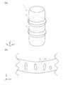
도 1(a)는 본 발명의 일실시형태에 의한 실장 구조체의 두께방향을 따른 단면도이며, 도 1(b)는 도 1(a)의 R1부분의 확대도이다.
도 2(a)는 본 발명의 일실시형태에 의한 실장 구조체의 스루홀의 형상을 나타내는 입체도이며, 도 2(b)는 본 발명의 일실시형태에 의한 실장 구조체의 스루홀의 내벽에 노출된 섬유의 표면도이다.
도 3(a)∼도 3(d)는 도 1(a)에 나타내는 실장 구조체의 제조 공정을 설명하는 두께방향으로 절단한 단면도이다.Fig. 1 (a) is a cross-sectional view along the thickness direction of a mounting structure according to an embodiment of the present invention, and Fig. 1 (b) is an enlarged view of a R1 portion in Fig.
FIG. 2 (a) is a three-dimensional view showing the shape of a through hole of a mounting structure according to an embodiment of the present invention, and FIG. 2 (b) .
3 (a) to 3 (d) are cross-sectional views taken along the thickness direction for explaining a manufacturing process of the mounting structure shown in Fig. 1 (a).
이하에, 본 발명의 일실시형태에 의한 배선 기판을 포함하는 실장 구조체를 도면에 의거해서 상세하게 설명한다.Hereinafter, a mounting structure including a wiring board according to an embodiment of the present invention will be described in detail with reference to the drawings.
도 1(a)에 나타낸 실장 구조체(1)는 예를 들면 각종 오디오비주얼 기기, 가전 기기, 통신 기기, 컴퓨터 장치 또는 그 주변 기기 등의 전자 기기에 사용되는 것이다. 이 실장 구조체(1)는 전자부품(2)과, 전자부품(2)이 범프(3)를 통해 플립칩 실장된 평판상의 배선 기판(4)을 포함하고 있다.The
전자부품(2)은 예를 들면 IC 또는 LSI 등의 반도체 소자이며, 모재가 예를 들면 실리콘, 게르마늄, 갈륨비소, 갈륨비소인, 질화갈륨 또는 탄화규소 등의 반도체 재료에 의해 형성되어 있다. 이 전자부품(2)은 두께가 예를 들면 0.1mm 이상 1mm 이하로 설정되어 있다.The
범프(3)는 예를 들면 납, 주석, 은, 금, 구리, 아연, 비스무트, 인듐 또는 알루미늄 등을 포함하는 땜납 등의 도전재료에 의해 구성되어 있다.The
배선 기판(4)은 평판상의 코어 기판(5)과, 코어 기판(5)의 양측에 형성된 한쌍의 배선층(6)을 포함하고 있다. 이 배선 기판(4)은 예를 들면 평면방향으로의 열팽창률이 전자부품(2)보다 크게 설정되어 있다.The
코어 기판(5)은 배선 기판(4)의 강도를 높이면서 한쌍의 배선층(6) 사이의 도통을 꾀하는 것이며, 두께방향으로 관통하는 스루홀(T)이 복수 형성된 평판상의 기체(7)와, 복수의 스루홀(T)의 내벽을 피복하는 원통상의 스루홀 도체(8)와, 스루홀 도체(8)에 둘러싸여진 영역에 형성된 기둥상의 절연체(9)를 포함하고 있다.The
기체(7)는 코어 기판(5)의 강성을 높이는 것이며, 도 1(a) 및 도 1(b)에 나타낸 바와 같이, 수지(10)와, 상기 수지에 피복된 무기 절연 입자(11)와, 상기 수지에 피복된 복수의 섬유(12)로 이루어지는 평판상의 기재(13)를 포함하고 있다.The
이 기체(7)에 있어서 기재(13) 및 상기 기재(13)의 섬유(12) 사이에 배치된 수지(10)로 이루어지는 층을 섬유층(14)으로 하고, 편의상 인접하는 2개의 섬유층(14)을 제 1 섬유층(14a), 제 2 섬유층(14b)으로 한다. 또한, 각 섬유층(14) 사이에 배치되어 섬유를 포함하지 않고, 수지(10) 및 무기 절연 입자(11)로 이루어지는 층을 수지층(15)으로 한다. 이 섬유층(14)과 수지층(15)의 경계는 섬유층(14)의 섬유(12)와 수지층(15)의 수지(10)의 계면에 의해 구성된다. 또한, 섬유층(14)은 섬유(12) 사이에 무기 절연 입자(11)를 포함해도 상관없다.In this
또한, 기체(7)는 두께가 예를 들면 0.03mm 이상 0.4mm 이하로 설정되고, 평면방향으로의 열팽창률이 예를 들면 4ppm/℃ 이상 15ppm/℃ 이하로 설정되고, 두께방향으로의 열팽창률이 예를 들면 11ppm/℃ 이상 30ppm/℃ 이하로 설정되고, 두께방향으로의 열팽창률이 평면방향으로의 열팽창률의 예를 들면 2배 이상 2.8배 이하로 설정되고, 영률이 예를 들면 20㎬ 이상 30㎬ 이하로 설정되어 있다.The thickness of the
여기에서, 기체(7)의 열팽창률은 시판의 TMA장치를 사용해서 JISK7197-1991에 준한 측정 방법에 의해 측정된다. 또한, 영률은 MTS 시스템즈사제 Nano Indentor XP/DCM을 사용해서 측정된다.Here, the coefficient of thermal expansion of the
기체(7)에 포함되는 수지(10)는 예를 들면 에폭시 수지, 비스말레이미드트리아진 수지, 시아네이트 수지, 폴리파라페닐렌벤즈비스옥사졸 수지, 전체 방향족 폴리아미드 수지, 폴리이미드 수지, 방향족 액정 폴리에스테르 수지, 폴리에테르에테르케톤 수지 또는 폴리에테르케톤 수지 등의 수지 재료에 의해 형성할 수 있다. 이 수지(10)는 평면방향 및 두께방향으로의 열팽창률이 예를 들면 20ppm/℃ 이상 50ppm/℃ 이하로 설정되고, 영률이 예를 들면 3㎬ 이상 10㎬ 이하로 설정되어 있다.The
수지(10)에 피복된 무기 절연 입자(11)는 기체(7)의 열팽창률을 저감시킴과 아울러 기체(7)의 강성을 높이는 것이며, 수산화알루미늄, 수산화마그네슘 또는 산화규소 등의 무기 절연 재료를 포함하고, 그 중에서도 열팽창률이나 영률 등의 특성이 유리섬유에 가까운 산화규소를 포함하는 것이 바람직하다. 그 결과, 수지층(15)의 열팽창률이나 영률을 섬유층(14)에 근접시킬 수 있다. 무기 절연 입자(11)가 산화규소를 포함하는 경우 무기 절연 입자(11)는 산화규소를 65중량% 이상 100중량% 이하 함유하는 것이 바람직하고, 산화규소 이외에 산화알루미늄, 산화마그네슘, 산화칼슘, 질화알루미늄, 수산화알루미늄 또는 탄산칼슘 등을 함유해도 상관없다.The
이 무기 절연 입자(11)는 예를 들면 구상으로 형성되어 있고, 입경이 예를 들면 0.5㎛ 이상 5.0㎛ 이하로 설정되고, 각 방향으로의 열팽창률이 예를 들면 2.7ppm/℃ 이상 6ppm/℃ 이하로 설정되고, 영률이 70㎬ 이상 85㎬ 이하로 설정되어 있다. 또한, 무기 절연 입자(11)로서 섬유를 가늘게 절단해서 입자상으로 한 것을 사용해도 상관없다.The
또한, 무기 절연 입자(11)는 수지층(15)에 있어서의 함유량이 40체적% 이상 75 체적% 이하로 설정되어 있는 것이 바람직하다. 그 결과, 무기 절연 입자(11)의 함유량이 40체적% 이상인 것에 의해 수지층(15)의 열팽창률 및 영률을 섬유층(14)에 근접시킬 수 있다. 또한, 무기 절연 입자(11)의 함유량이 70체적% 이상인 것에 의해 스루홀(T) 내벽에 위치하는 무기 절연 입자(11)와 수지(10)의 접착 강도를 높이고, 상기 무기 절연 입자(11)와 수지(10)의 박리를 저감시키고, 나아가서는 스루홀 도체(8)와 수지층(15)의 박리를 저감시킬 수 있다.It is preferable that the content of the
여기에서, 무기 절연 입자(11)의 입경은 기체(7)의 단면을 전계방출형 전자현미경으로 관찰하고, 각 입자의 최대 지름을 계측하고, 그 평균값을 산출함으로써 측정된다. 또한, 수지층(15)에 있어서의 무기 절연 입자(11)의 함유량(체적%)은 수지층(15)의 단면을 전계방출형 전자현미경으로 관찰하고, 수지층(15)에 대해서 무기 절연 입자(11)가 차지하는 면적비율(면적%)을 계측하고, 그 평균값을 산출해서 함유량(체적%)으로 간주함으로써 측정된다.Here, the particle diameter of the
수지(10)에 피복된 기재(13)는 기체(7)의 강성을 높임과 아울러 평면방향으로의 열팽창률을 저감시키는 것이며, 예를 들면, 복수의 섬유(12)가 종횡으로 짜여져서 이루어지는 직포를 사용할 수 있다. 또한, 기재(13)로서 부직포를 사용해도 상관없고, 복수의 섬유(12)를 길이방향이 서로 평행하게 되도록 배열한 것을 사용해도 상관없다.The
기재(13)에 포함되는 섬유(12)는 T유리 또는 E유리 등의 유리섬유를 사용할 수 있고, 길이방향에 수직인 단면의 지름이 예를 들면 4㎛ 이상 9㎛ 이하로 설정되어 있고, 길이방향 및 폭방향으로의 열팽창률이 2.5ppm/℃ 이상 6ppm/℃ 이하로 설정되고, 영률이 70㎬ 이상 85㎬ 이하로 설정되어 있다.The
한편, 스루홀(T) 내벽에 피착된 스루홀 도체(8)는 코어 기판(5) 상하의 배선층(6)끼리를 전기적으로 접속하는 것이며, 예를 들면 구리, 알루미늄 또는 니켈 등의 도전재료에 의해 형성된 것을 사용할 수 있다. 이 스루홀 도체(8)는 스루홀(T) 내벽으로부터 절연체(9)까지의 길이가 3㎛ 이상 20㎛ 이하로 설정되어 있고, 관통방향 및 폭방향으로의 열팽창률이 예를 들면 16ppm/℃ 이상 25ppm/℃ 이하로 설정되고, 영률이 예를 들면 60㎬ 이상 210㎬ 이하로 설정되어 있다. 또한, 스루홀 도체(8)의 열팽창률 및 영률은 기체(7)와 동일하게 측정된다.On the other hand, the through-
스루홀 도체(8)에 둘러싸여진 영역에 형성된 절연체(9)는 후술하는 비아 도체(18)의 지지면을 형성하는 것이며, 예를 들면 폴리이미드 수지, 아크릴 수지, 에폭시 수지, 시아네이트 수지, 불소 수지, 실리콘 수지, 폴리페닐렌에테르 수지 또는 비스말레이미드트리아진 수지 등의 수지 재료에 의해 형성할 수 있다.The
한편, 코어 기판(5)의 양측에는 상술한 바와 같이 한쌍의 배선층(6)이 형성되어 있다. 배선층(6)은 기체(7) 상에 적층되고, 두께방향으로 관통하는 비아 구멍(V)이 형성된 절연층(16)과, 기체(7) 상 또는 절연층(16) 상에 형성된 도전층(17)과, 비아 구멍(V) 내에 형성되어 도전층(17)에 전기적으로 접속된 비아 도체(18)를 포함하고 있다.On the other hand, on both sides of the
절연층(16)은 도전층(17)을 지지하는 지지 부재로서 기능할 뿐만 아니라, 도전층(17)끼리의 단락을 방지하는 절연 부재로서 기능하는 것이며, 수지와, 상기 수지에 피복된 무기 절연 입자를 포함하고 있다. 이 절연층(16)은 두께가 예를 들면 5㎛ 이상 40㎛ 이하로 설정되고, 평면방향 및 두께방향으로의 열팽창률이 예를 들면 15ppm/℃ 이상 45ppm/℃ 이하로 설정되고, 영률이 예를 들면 5㎬ 이상 40㎬ 이하로 설정되어 있다. 또한, 절연층(16)의 열팽창률 및 영률은 기체(7)와 동일하게 측정된다.The insulating
절연층(16)에 포함되는 수지로서는 예를 들면 에폭시 수지, 비스말레이미드트리아진 수지, 시아네이트 수지, 폴리파라페닐렌벤즈비스옥사졸 수지, 전체 방향족 폴리아미드 수지, 폴리이미드 수지, 방향족 액정 폴리에스테르 수지, 폴리에테르에테르케톤 수지 또는 폴리에테르케톤 수지 등에 의해 형성된 것을 사용할 수 있다.Examples of the resin included in the insulating
절연층(16)에 포함되는 무기 절연 입자로서는 기체(7)에 포함되는 무기 절연 입자(11)와 동일한 것을 사용할 수 있다.As the inorganic insulating particles contained in the insulating
도전층(17)은 예를 들면 접지용 배선, 전력 공급용 배선 또는 신호용 배선으로서 기능하는 것이며, 예를 들면 구리, 은, 금, 알루미늄, 니켈 또는 크롬 등의 금속재료에 의해 형성된 것을 사용할 수 있다. 이 도전층(17)은 두께가 예를 들면 3㎛ 이상 20㎛ 이하로 설정되고, 평면방향 및 두께방향으로의 열팽창률이 예를 들면 5ppm/℃ 이상 25ppm/℃ 이하로 설정되고, 영률이 50㎬ 이상 250㎬ 이하로 설정되어 있다.The
비아 도체(18)는 두께방향으로 서로 이간된 도전층(17)끼리를 서로 접속하는 것이며, 예를 들면 폭이 코어 기판(5)을 향해서 작아지는 테이퍼상으로 형성되어 있고, 예를 들면 구리, 은, 금, 알루미늄, 니켈 또는 크롬의 도전 재료에 의해 형성된 것을 사용할 수 있다.The via
그런데, 기체(7)는 열팽창률이 다른 섬유층(14) 및 수지층(15)을 포함하기 때문에 스루홀(T)의 내벽은 열팽창률이 스루홀(T)의 관통방향(Z방향)에 있어서 국소적으로 다르다. 그 때문에, 전자부품(2)의 실장시나 작동시에 열이 배선 기판(4)에 인가되었을 때에 스루홀(T)의 내벽과 스루홀 도체(8) 사이에 열응력이 인가되기 쉽다.Since the
한편, 본 실시형태의 배선 기판(4)에 있어서는 도 1(b)에 나타낸 바와 같이, 스루홀(T)의 내벽은 기체(7)를 두께방향에 있어서 단면으로 봤을 때 수지층(15)에 제 1 섬유층(14a) 및 제 2 섬유층(14b)과의 경계를 양단부로 하는 곡선상의 오목부(D)를 갖고, 상기 오목부(D)의 내측에는 스루홀 도체(8)의 일부가 충전되어 있다.On the other hand, in the
그 결과, 오목부(D) 내측에 스루홀 도체(8)의 일부가 충전되어 있기 때문에 스루홀(T)의 관통방향으로 앵커 효과가 발생되어 스루홀(T)의 내벽과 스루홀 도체(8)의 접착 강도를 높일 수 있고, 스루홀(T)의 내벽과 스루홀 도체(8)의 박리를 저감시키고, 나아가서는 스루홀 도체(8)의 단선을 저감시킬 수 있다.As a result, since a part of the through-
또한, 오목부(D)는 수지층(15)과 제 1 섬유층(14a)의 경계, 및 수지층(15)과 제 2 섬유층(14b)의 경계에 양단부(E1,E2)를 갖는 곡선상이기 때문에 각각의 경계에 있어서 섬유층(14)의 섬유(12)에 대한 수지층(15)의 수지(10)의 피복 영역을 유지하면서 오목부(D)를 형성할 수 있다. 그 결과, 오목부(D) 내측에 대한 섬유(12) 측면(기체(7)의 평면방향으로 평행한 면)의 노출 영역을 저감시키고, 상기 노출 영역을 기점으로 한 섬유(12)와 수지(10)의 박리를 저감시킴으로써 스루홀 도체(8)의 마이그레이션을 저감시키고, 인접하는 스루홀 도체(8) 사이의 단락을 저감시키고, 나아가서는 전기적 신뢰성이 우수한 배선 기판(4)을 얻을 수 있다.The concave portion D is a curved line having both ends E1 and E2 at the boundary between the
이 오목부(D)는 양단부(E1,E2)를 연결하는 가상 직선(L)으로부터의 깊이가 1㎛ 이상 5㎛ 이하로 설정되어 있는 것이 바람직하다. 그 결과, 상기 깊이가 1㎛ 이상인 것에 의해 오목부(D)의 앵커 효과를 높일 수 있다. 또한, 상기 깊이가 5㎛ 이하인 것에 의해 상기 오목부(D)의 저부에서 인접하는 스루홀(T) 사이의 절연성을 높이면서 섬유(12)의 측면의 오목부(D)에 대한 노출을 저감시킴과 아울러 섬유(12)와 수지(10)의 박리를 저하시킬 수 있다.It is preferable that the depth of the concave portion D from the imaginary straight line L connecting the both ends E1 and E2 is set to be not less than 1 탆 and not more than 5 탆. As a result, when the depth is 1 mu m or more, the anchor effect of the concave portion D can be enhanced. The depth of 5 mu m or less makes it possible to reduce the exposure of the side surface of the
또한, 오목부(D)의 양단부(E1,E2)는 각각 제 1 섬유층(14a) 및 제 2 섬유층(14b)의 가장자리에 위치하는 것이 바람직하다. 그 결과, 수지층(15)과 섬유층(14)의 경계에 위치하는 섬유(12)의 측면을 기체(7)측으로부터 스루홀(T)측(XY 평면방향)을 지나 수지층(15)의 수지(10)로 피복할 수 있고, 오목부(D) 내측에 대한 섬유(12) 측면의 노출을 없애서 섬유(12)와 수지(10)의 박리를 저감시킬 수 있다.It is preferable that both end portions E1 and E2 of the concave portion D are located at the edges of the first and second
또한, 오목부(D)는 도 2(a)에 나타낸 바와 같이, 스루홀(T)의 주회방향을 지나 형성되어 있는 것이 바람직하다. 그 결과, 스루홀(T)의 관통방향(Z방향)에 있어서의 앵커 효과를 향상시킬 수 있다.2 (a), it is preferable that the concave portion D is formed to extend through the through-hole T in the main-scanning direction. As a result, the anchor effect in the penetration direction (Z direction) of the through hole T can be improved.
한편, 본 실시형태의 배선 기판(4)에 있어서는 도 1(b)에 나타낸 바와 같이, 제 1 섬유층(14a) 및 제 2 섬유층(14b)의 섬유(12)는 스루홀(T) 내벽에 노출된 면(스루홀(T)의 관통방향으로 평행한 면)이 요철을 갖고 있고, 상기 요철의 오목부(C)의 내측에는 스루홀 도체(8)의 일부가 충전되어 있다. 그 결과, 스루홀 도체(8)와 비교해서 열팽창률이 작은 유리섬유로 이루어지는 섬유(12)에 있어서도 앵커 효과가 발생되기 때문에 스루홀(T) 내벽과 스루홀 도체(8)의 접착 강도를 높일 수 있다.On the other hand, in the
섬유(12)의 스루홀(T) 내벽에 노출된 면의 산술 평균 거칠기(Ra)는 예를 들면 0.3㎛ 이상 3㎛ 이하로 설정되어 있다. 또한, 섬유(12)의 수지층(15)과 섬유층(14)의 경계에 위치하는 측면(기체(7)의 평면방향으로 평행한 면)의 산술 평균 거칠기는 예를 들면 0.1㎛ 이하로 설정되어 있고, 섬유(12)의 스루홀(T) 내벽에 노출된 면의 산술 평균 거칠기보다 작다.The arithmetic mean roughness Ra of the surface exposed to the inner wall of the through hole T of the
또한, 오목부(C)는 도 2(b)에 나타낸 바와 같이, 가늘고 긴 형상이며, 기체(7)의 두께방향을 따르는 홈상인 것이 바람직하다. 그 결과, 스루홀 도체(8)와 비교해서 평면으로 볼 때에 있어서의 열팽창량이 작은 섬유(12)에 있어서 스루홀(T)의 주회방향에 있어서의 앵커 효과를 발생시키기 때문에 스루홀(T) 내벽과 스루홀 도체(8)의 접착 강도를 높일 수 있다.2 (b), it is preferable that the concave portion C has a slender shape and is a groove shape along the thickness direction of the
이 오목부(C)는 신장방향의 길이가 예를 들면 3㎛ 이상 8㎛ 이하로 설정되고, 폭이 예를 들면 2㎛ 이상 5㎛ 이하로 설정되고, 깊이가 예를 들면 0.5㎛ 이상 3㎛ 이하로 설정되어 있다. 또한, 오목부(C)는 신장방향의 길이에 대한 폭의 비율이 예를 들면 40% 이상 80% 이하로 설정되어 있다.The depth of the concave portion C is set to, for example, not less than 3 占 퐉 and not more than 8 占 퐉, the width is set to, for example, not less than 2 占 퐉 and not more than 5 占 퐉, Or less. The ratio of the width of the concave portion C to the length in the stretching direction is set to, for example, 40% or more and 80% or less.
이렇게 해서 상술한 실장 구조체(1)는 배선 기판(4)을 통해 공급되는 전원이나 신호에 의거해서 전자부품(2)을 구동 또는 제어함으로써 소망의 기능을 발휘한다.Thus, the above-described
이어서, 상술한 실장 구조체(1)의 제조 방법을 도 3에 의거해서 설명한다.Next, a manufacturing method of the above-described
(기체의 준비)(Preparation of gas)
(1)도 3(a)에 나타낸 바와 같이, 기체(7)와 상기 기체(7)의 상하에 배치된 동박(17x)으로 이루어지는 동장 적층판(5x)을 준비한다. 구체적으로는 예를 들면 이하와 같이 행한다.(1) As shown in Fig. 3 (a), a copper clad laminate 5x composed of a
우선, 미경화의 수지(10) 및 무기 절연 입자(11)를 포함하는 바니시를 준비하고, 상기 바니시를 기재(12)에 함침시켜서 수지 시트를 형성한다. 이렇게 바니시를 기재(12)에 함침시킬 때에 무기 절연 입자(11)가 기재(13)의 섬유(12) 사이에 침입하기 어렵기 때문에 기재(13) 밖의 영역(수지층(15)이 되는 영역)에 농축된다. 또한, 미경화는 ISO472:1999에 준하는 A-스테이지 또는 B-스테이지의 상태이다.First, a varnish containing
이어서, 상기 수지 시트를 적층해서 기체 전구체를 형성함과 아울러 상기 기체 전구체의 상하에 동박(17x)을 적층해서 적층체를 형성한 후 상기 적층체를 두께방향으로 가열 가압함으로써 상기 수지(10)를 열경화시켜서 기체(7)를 형성함과 아울러 상술한 동장 적층판(5x)을 제작한다. 이렇게 기체(7)를 형성할 때에 수지 시트의 기재(13) 및 그 섬유(12) 간의 수지가 섬유층(14)이 되고, 인접하는 수지 시트의 기재(13) 밖의 영역끼리가 접착해서 수지층(15)이 된다.Subsequently, the resin sheet is laminated to form a gas precursor, and a
(스루홀의 형성)(Formation of through hole)
(2)도 3(b)에 나타낸 바와 같이, 샌드 블라스트법을 사용해서 동장 적층판(5x)에 스루홀(T)을 형성한다. 구체적으로는 예를 들면 이하와 같이 행한다.(2) As shown in Fig. 3 (b), a through hole T is formed in the copper clad laminate 5x by sandblasting. Specifically, for example, the following operation is performed.
우선, 동장 적층판(5x)의 양면에 스루홀(T)의 형성 개소에 개구를 갖는 레지스트를 형성한다. 이 레지스트는 예를 들면 감광성 수지의 노광, 현상에 의해 형성할 수 있다. 이어서, 샌드 블라스트 장치의 노즐로부터 동장 적층판(5x)의 일주면에 미립자를 분사함으로써 상기 레지스트의 개구를 통해 스루홀(T)의 일부분(비관통)을 형성한다. 이어서, 동장 적층판(5x)의 타주면에 미립자를 분사함으로써 기체(7)를 관통하는 스루홀(T)을 형성한다. 또한, 기체(7)를 관통하는 스루홀(T)은 동장 적층판(5x)의 일주면에만 미립자를 분사함으로써 형성해도 상관없다. 이어서, 레지스트를 예를 들면 1wt% 수산화나트륨 용액 등으로 제거한다. 이어서, 스루홀(T)의 내벽을 고압 수세함으로써 잔존한 미립자나 스루홀(T)의 가공 부스러기를 제거한다.First, a resist having openings is formed on the both surfaces of the copper-clad laminate 5x at portions where the through-holes T are formed. The resist can be formed, for example, by exposure and development of a photosensitive resin. Subsequently, fine particles are jetted from the nozzles of the sandblasting apparatus onto one main surface of the copper clad laminate 5x to form a portion (non-through) of the through holes T through the openings of the resist. Subsequently, fine pellets are sprayed on the rubbing surface of the copper-plated laminated board 5x to form a through hole T passing through the
이렇게, 본 실시형태의 배선 기판(4)의 제조 방법에 있어서는 샌드 블라스트법에 의해 섬유층(14) 및 수지층(15)을 포함하는 기체(7)에 스루홀(T)을 형성하고 있다. 여기에서, 기체(7)의 섬유층(14)은 유리로 이루어지는 섬유(12)을 포함하기 때문에 수지층(15)과 비교해서 샌드 블라스트법에 의해 절삭되기 어렵다. 그 때문에, 분사한 미립자끼리가 충돌해서 산란하면 기체(7)의 내부측을 향해서 수지층(15)을 섬유층(14)보다 크게 절삭하기 때문에 수지층(15)에 있어서의 스루홀(T)의 내벽에 오목부(D)를 형성할 수 있다.Thus, in the method of manufacturing the
또한, 이 오목부(D)는 기체(7)의 두께방향에 있어서의 단면에서 곡선상으로 형성된다. 이것은 샌드 블라스트법으로 기체(7)를 절삭할 때에 수지층(15) 직상의 제 1 섬유층(14a)이 스루홀(T)측으로 돌출하므로 샌드 블라스트 장치로부터 분사된 미립자가 제 1 섬유층(14a)으로부터 멀어짐에 따라서 기체(7)의 내부측에 도달하기 쉬워져 오목부(D)를 깊게 형성하기 쉬워지는 한편, 수지층(15) 직하의 제 2 섬유층(14b)이 스루홀(T)측으로 돌출되므로 절삭시의 저부에서 반사된 미립자가 제 2 섬유층(14b)으로부터 멀어짐에 따라서 기체(7)의 내부측에 도달하기 쉬워져 오목부(D)를 깊게 형성하기 쉬워지는 점에서 곡선상의 오목부(D)가 형성된다고 추측된다.The concave portion D is formed in a curved shape in the cross-section in the thickness direction of the
또한, 기체(7)의 두께방향을 따라 분사된 미립자에 의해 스루홀(T)의 내벽에 노출된 섬유층(12)의 면이 부분적으로 절삭되기 때문에 두께방향을 따르는 홈상의 오목부(C)를 형성할 수 있다.Since the surface of the
또한, 레지스트를 사용하고 있는 점에서 미립자를 광범위하게 분사해서 복수의 스루홀(T)을 동시에 가공할 수 있으므로 드릴 가공이나 레이저 가공과 비교해서 스루홀(T)를 효율 좋게 형성할 수 있다. 특히, 기체(7)의 두께가 0.03mm 이상 0.4mm 이하로 얇게 설정되어 있으면 샌드 블라스트법을 사용해서 효율 좋게 스루홀(T)을 형성할 수 있다.Further, since the resist is used, it is possible to simultaneously process the plurality of through holes T by spraying the fine particles in a wide range, so that the through hole T can be formed efficiently as compared with the drilling or laser processing. Particularly, if the thickness of the
또한, 미립자에 의해 스루홀(T)을 형성하기 때문에 드릴 가공과 비교해서 섬유(12)와 수지(10)의 경계에 인가되는 응력 및 열(드릴 가공의 마찰열)을 저감시킬 수 있고, 또한 레이저 가공과 비교해서 섬유(12)와 수지(10)의 경계에 인가되는 열을 저감시킬 수 있기 때문에 섬유(12)와 수지(10)의 박리를 저감시킬 수 있다.Since the through holes T are formed by the fine particles, stress and heat applied to the boundary between the
또한, 샌드 블라스트법을 사용하면 기체(7)에 있어서의 무기 절연 필러(11)의 함유량을 증가시켰을 경우에 드릴 가공과 같이 드릴이 마모되지 않고, 또한 레이저 가공보다 용이하게 스루홀(T)을 형성할 수 있다.When the sand blasting method is used, when the content of the inorganic insulating
이상과 같이 샌드 블라스트법으로 스루홀(T) 및 오목부(D)를 형성하기 때문에 샌드 블라스트법은 이하의 조건으로 행할 수 있다.As described above, since the through hole T and the concave portion D are formed by the sandblasting method, the sandblasting method can be performed under the following conditions.
우선, 샌드 블라스트법은 드라이 블라스트에 의해 행해진다. 그 결과, 웨트 블라스트와 비교해서 미립자에 대한 저항이 작기 때문에 스루홀(T)의 절삭 효율을 높임과 아울러 절삭시의 가공 부스러기의 잔류를 저감시켜 상기 가공 부스러기에 의한 절삭 저해를 저감시킬 수 있다.First, the sand blast method is performed by dry blasting. As a result, since the resistance to the fine particles is small as compared with the wet blast, the cutting efficiency of the through hole (T) is increased, and the residual of the machining debris at the time of machining is reduced, so that the inhibition of cutting by the machining debris can be reduced.
또한, 분사에 사용되는 미립자는 알루미나, 유리 또는 탄화규소 등의 무기 절연 재료로 이루어지는 구상 입자 또는 파쇄 입자를 사용할 수 있다. 그 중에서도 알루미나 등의 유리 섬유보다 경도가 높은 파쇄 입자를 사용하는 것이 바람직하다. 그 결과, 단단한 파쇄 입자의 뾰족한 끝부에 의해 스루홀(T)의 내벽에 노출된 섬유(12)의 면이 부분적으로 절삭되기 때문에 스루홀(T)의 절삭 효율을 높임과 아울러 오목부(C)를 양호하게 형성할 수 있다. 또한, 파쇄 입자는 예를 들면, 무기 절연 재료로 이루어지는 구조체를 파쇄함으로써 형성할 수 있다.The fine particles used for injection may be spherical particles or crushed particles made of an inorganic insulating material such as alumina, glass, or silicon carbide. Among them, it is preferable to use crushed particles having a hardness higher than that of glass fibers such as alumina. As a result, since the surface of the
또한, 미립자의 입경은 10㎛ 이상 30㎛ 이하로 설정되어 있다. 그 결과, 입경을 10㎛ 이상으로 함으로써 스루홀(T)의 절삭 효율을 높임과 아울러 수지층(15)의 절삭 효율을 높여 오목부(D)를 양호하게 형성할 수 있다. 또한, 입경을 30㎛ 이하로 함으로써 1개의 미립자에 의한 섬유(12)의 절삭량을 저감시켜 오목부(D)를 양호하게 형성할 수 있다. 또한, 미립자의 입경은 각 입자의 최대 지름의 평균값이다.The particle size of the fine particles is set to 10 μm or more and 30 μm or less. As a result, by setting the grain size to 10 mu m or more, the cutting efficiency of the through hole (T) can be increased, and the cutting efficiency of the resin layer (15) can be increased to form the concave portion (D) well. In addition, by setting the particle diameter to be 30 占 퐉 or less, the amount of cut of the
또한, 미립자를 분사하는 압력은 0.15㎫ 이상 0.22㎫ 이하로 설정되어 있다. 그 결과, 압력을 0.15㎫ 이상으로 함으로써 스루홀(T)의 절삭 효율을 높임과 아울러 미립자끼리가 충돌해서 산란함으로써 기체(7)의 내부측을 향해서 수지층(15)을 크게 절삭해서 오목부(D)를 양호하게 형성할 수 있다. 또한, 압력을 0.22㎫ 이하로 함으로써 1개의 미립자에 의한 섬유(12)의 절삭량을 저감시켜 오목부(D)를 양호하게 형성할 수 있다.The pressure for spraying the fine particles is set to 0.15 MPa or more and 0.22 MPa or less. As a result, by setting the pressure to 0.15 MPa or more, the cutting efficiency of the through hole (T) is increased, and the fine particles collide with each other and scatter to greatly cut the resin layer (15) toward the inner side of the substrate (7) D) can be satisfactorily formed. Further, by setting the pressure to 0.22 MPa or less, the amount of cut of the
또한, 1개의 스루홀(T)에 대해서 미립자를 분사하는 횟수(스캔 횟수)는 기체(7)의 두께에 따라서 설정되고, 예를 들면 코어 기판(5)의 두께가 80㎛ 이상 400㎛ 이하인 경우에는 4회 이상 20회 이하로 설정되어 있다.The number of times (the number of times of scanning) that the fine particles are injected into one through hole T is set in accordance with the thickness of the
또한, 미립자를 분사하는 기체(7)의 수지층(15)은 무기 절연 입자(11)의 함유량이 40체적% 이상 75체적% 이하로 설정되어 있다. 그 결과, 무기 절연 입자(11)의 함유량을 40체적% 이상으로 함으로써 샌드 블라스트법에 의한 수지층(15)의 절삭 효율을 높일 수 있기 때문에 스루홀(T)의 절삭 효율을 높임과 아울러 오목부(D)를 양호하게 형성할 수 있다. 또한, 무기 절연 입자(11)의 함유량을 75체적% 이하로 함으로써 무기 절연 입자(11)의 탈립을 저감시켜 오목부(D)가 과잉으로 깊어지는 것을 저감시킬 수 있다.In addition, the content of the inorganic insulating
이상 설명한 조건으로 샌드 블라스트법을 행함으로써 스루홀(T) 및 오목부(D)를 양호하게 형성할 수 있다.By performing the sandblasting method under the above-described conditions, the through hole T and the concave portion D can be formed well.
또한, 상술한 (1)의 공정에서 기체(7)의 상하면에 동박(17x)을 형성하고 있다. 그 결과, 동박(17x)이 섬유층(14) 및 수지층(15)보다 샌드 블라스트법에 의해 절삭되기 어렵기 때문에 상기 동박(17x)에 의해 스루홀(T)의 개구 지름을 작게 할 수 있다.The
여기에서, 샌드 블라스트법으로 형성된 스루홀(T)의 내벽은 디스미어 처리를 행하지 않는 것이 바람직하다. 샌드 블라스트법으로 스루홀(T)을 형성하면 드릴 가공이나 레이저 가공과 비교해서 스루홀(T)의 내벽에 인가되는 열을 저감시켜 탄화된 수지의 잔재를 저감시킬 수 있음과 아울러 물리적으로 분자간의 결합이 절단되기 때문에 스루홀(T) 내벽의 반응 활성을 높일 수 있다. 그 때문에, 디스미어 처리를 행하지 않더라도 스루홀(T)의 내벽과 스루홀 도체(8)의 접착 강도를 높일 수 있다. 이렇게 디스미어 처리를 행하지 않음으로써 수지(10)만이 선택적으로 에칭되어서 섬유(12)의 측면이 크게 노출되는 것을 저감시켜 수지(10)와 섬유(12)의 박리를 저감시킬 수 있다. 또한, 디스미어를 행하지 않음으로써 오목부(D)의 형상을 유지할 수 있고, (3)의 공정에서 스루홀 도체(8)의 일부를 오목부(D)에 충전할 수 있다.Here, it is preferable that the inner wall of the through hole T formed by the sandblasting method does not perform the desmear treatment. When the through hole T is formed by the sandblasting method, the heat applied to the inner wall of the through hole T is reduced as compared with the drilling or laser processing, so that the remnants of the carbonized resin can be reduced, It is possible to increase the reaction activity of the inner wall of the through hole (T). Therefore, even if the desmear treatment is not performed, the bonding strength between the inner wall of the through hole (T) and the through hole conductor (8) can be increased. By not performing the desmearing treatment in this way, only the
(스루홀 도체의 형성)(Formation of through-hole conductor)
(3)도 3(c)에 나타낸 바와 같이, 기체(7)에 스루홀 도체(8), 절연체(9) 및 도전층(17)을 형성해서 코어 기판(5)을 제작한다. 구체적으로는 예를 들면 이하와 같이 행한다.(3) As shown in Fig. 3 (c), the through-
우선, 예를 들면 무전해 도금법, 전해 도금법, 증착법, CVD법 또는 스퍼터링법 등에 의해 스루홀(T)의 내벽에 도전 재료를 피착시켜서 원통상의 스루홀 도체(8)를 형성한다. 이 때, 상기 도전 재료는 스루홀(T) 내벽의 오목부(D)에 충전된다. 이어서, 원통상의 스루홀 도체(8)에 의해 둘러싸여진 영역에 수지 재료 등을 충전해서 절연체(9)를 형성한다. 이어서, 절연체(9)의 노출부에 도전 재료를 피착시킨 후 종래 주지의 포토리소그래피 기술, 에칭 등에 의해 동박(17x)을 패터닝 해서 도전층(17)을 형성한다.First, a conductive material is deposited on the inner wall of the through hole T by, for example, an electroless plating method, an electrolytic plating method, a vapor deposition method, a CVD method, a sputtering method, or the like to form a cylindrical through-
이상과 같이 해서 코어 기판(5)을 제작할 수 있다.The
(배선층의 형성)(Formation of wiring layer)
(4)도 3(d)에 나타낸 바와 같이, 코어 기판(5)의 양측에 한쌍의 배선층(6)을 형성함으로써 배선 기판(4)을 제작한다. 구체적으로는 예를 들면 이하와 같이 행한다.(4) As shown in Fig. 3 (d), a
우선, 미경화의 수지를 도전층(17) 상에 배치하고, 수지를 가열해서 유동 밀착시키면서 더욱 가열해서 수지를 경화시킴으로써 도전층(17) 상에 절연층(16)을 형성한다. 이어서, 레이저 가공으로 비아 구멍(V)을 형성하고, 비아 구멍(V) 내에 도전층(17)의 적어도 일부를 노출시킨다. 이렇게, 레이저 가공으로 비아 구멍(V)을 형성함으로써 샌드 블라스트법과 비교해서 비아 구멍(V) 내에 노출시키는 도전층(17)의 손상을 저감시킬 수 있다. 이어서, 예를 들면 세미 애디티브법, 서브트랙티브법 또는 풀 애디티브법 등에 의해 비아 구멍(V)에 비아 도체(18)를 형성함과 아울러 절연층(16)의 상면에 도전층(17)을 형성한다.First, an uncured resin is placed on the
이상과 같이 해서, 배선 기판(4)을 제작할 수 있다. 또한, 본 공정을 반복함으로써 배선층(6)에 있어서 절연층(16) 및 도전층(17)을 다층화시킬 수 있다.Thus, the
(전자부품의 실장)(Mounting of electronic parts)
(5)최상층의 도전층(17) 상면에 범프(3)를 형성함과 아울러 범프(3)를 통해 배선 기판(4)에 전자부품(2)을 플립칩 실장한다.(5) The
이상과 같이 해서, 도 1(a)에 나타낸 실장 구조체(1)를 제작할 수 있다.In this way, the mounting
본 발명은 상술한 실시형태에 한정되는 것은 아니고, 본 발명의 요지를 일탈하지 않는 범위에 있어서 여러가지의 변경, 개량, 조합 등이 가능하다.The present invention is not limited to the above-described embodiments, and various changes, improvements, combinations, and the like can be made without departing from the gist of the present invention.
예를 들면, 상술한 실시형태에 있어서 전자부품에 반도체 소자를 사용한 구성을 예로 설명했지만, 전자부품으로서는 콘덴서 등을 사용해도 상관없다.For example, in the above-described embodiment, a configuration using a semiconductor element as an electronic component is described as an example, but a capacitor or the like may be used as an electronic component.
또한, 상술한 실시형태에 있어서 전자부품을 배선 기판 상에 플립칩 실장한 구성을 예로 설명했지만, 전자부품을 배선 기판에 와이어 본딩 실장해도 상관없고, 전자부품을 배선 기판의 내부에 실장해도 상관없다.In the above-described embodiment, the electronic component is flip-chip mounted on the wiring board. However, the electronic component may be wire-bonded to the wiring board, and the electronic component may be mounted inside the wiring board .
또한, 상술한 실시형태에 있어서 배선층이 절연층을 1층 포함하는 구성을 예로 설명했지만, 배선층은 절연층을 수층 포함해도 상관없다.In the above-described embodiment, the wiring layer includes one insulating layer as an example. However, the wiring layer may include an insulating layer as an aqueous layer.
또한, 상술한 실시형태에 있어서 기체가 섬유층을 3층 포함하는 구성을 예로 설명했지만, 기체는 섬유층을 수층 포함해도 상관없다.In the above-described embodiment, the gas has three layers of fibrous layers. However, the base layer may include the fibrous layer.
또한, 상술한 실시형태에 있어서 섬유층의 수지와 수지층의 수지가 동일한 것인 구성을 예로 설명했지만, 섬유층의 수지와 수지층의 수지는 다른 것이라도 상관없다.In the above embodiment, the resin of the fiber layer and the resin of the resin layer are the same. However, the resin of the fiber layer and the resin of the resin layer may be different.
또한, 상술한 실시형태에 있어서 (1)의 공정에서 동박을 사용한 구성을 예로 설명했지만, 동박 대신에, 예를 들면 철니켈 합금 또는 철니켈코발트 합금 등의 금속 재료로 이루어지는 금속박을 사용해도 상관없다.In the above-described embodiment, the configuration using the copper foil in the step (1) has been described as an example. However, a metal foil made of a metal material such as an iron nickel alloy or an iron nickel cobalt alloy may be used instead of the copper foil .
1:실장 구조체 2:전자부품
3:범프 4:배선 기판
5:코어 기판 6:배선층
7:기체 8:스루홀 도체
9:절연체 10:수지
11:무기 절연 입자 12:섬유
13:기재 14:섬유층
15:수지층 16:절연층
17:도전층 18:비아 도체
T:스루홀 V:비아 구멍
D:오목부 E1, E2:단부
L:가상 곡선 C:오목부1: mounting structure 2: electronic parts
3: bump 4: wiring board
5: core substrate 6: wiring layer
7: gas 8: through-hole conductor
9: Insulator 10: Resin
11: inorganic insulating particle 12: fiber
13: substrate 14: fibrous layer
15: resin layer 16: insulating layer
17: conductive layer 18: via conductor
T: Through hole V: Via hole
D: recess E1, E2: end
L: virtual curve C: concave
Claims (7)
Translated fromKorean상기 기체는 복수의 섬유와 상기 복수의 섬유 사이에 배치된 수지를 각각 포함하는 제 1 섬유층 및 제 2 섬유층과, 이들 제 1 섬유층 및 제 2 섬유층 사이에 배치된 섬유를 포함하지 않고 수지를 포함하는 수지층을 갖고,
상기 스루홀의 내벽은 상기 기체를 두께방향에 있어서 단면으로 봤을 때 상기 수지층에 상기 제 1 섬유층 및 상기 제 2 섬유층과의 경계를 양단부로 하는 곡선상의 오목부를 갖고, 상기 오목부의 내측에는 상기 스루홀 도체의 일부가 충전되어 있고,
상기 오목부는 상기 스루홀 내에 미립자를 분사하여 상기 수지층을 상기 제 1 섬유층 및 상기 제 2 섬유층보다 더 오목하게 절삭하여 형성하는 것을 특징으로 하는 배선 기판.A through hole penetrating through the base in the thickness direction, and a through hole conductor covering the inner wall of the through hole,
Wherein the base body includes a first fiber layer and a second fiber layer each including a plurality of fibers and a resin disposed between the plurality of fibers and a resin containing no resin disposed between the first fiber layer and the second fiber layer Having a resin layer,
Wherein an inner wall of the through hole has a curved concave portion having a boundary between the first fibrous layer and the second fibrous layer at both ends in the resin layer when viewed in cross section in the thickness direction of the base, A portion of the conductor is charged,
Wherein the concave portion is formed by cutting fine particles into the through hole to cut the resin layer more concave than the first fiber layer and the second fiber layer.
상기 오목부는 상기 양단부를 연결하는 가상 직선으로부터의 깊이가 1㎛ 이상 5㎛ 이하인 것을 특징으로 하는 배선 기판.The method according to claim 1,
Wherein the concave portion has a depth from a virtual straight line connecting the both end portions of 1 占 퐉 or more to 5 占 퐉 or less.
상기 오목부의 상기 양단부는 각각 상기 제 1 섬유층 및 상기 제 2 섬유층의 가장자리에 위치하고 있는 것을 특징으로 하는 배선 기판.The method according to claim 1,
And the both end portions of the concave portion are located at edges of the first fiber layer and the second fiber layer, respectively.
상기 제 1 섬유층 및 상기 제 2 섬유층의 상기 섬유는 상기 스루홀의 내벽에 노출된 면이 요철을 갖고 있고,
상기 요철의 오목부의 내측에는 상기 스루홀 도체의 일부가 충전되어 있는 것을 특징으로 하는 배선 기판.The method according to claim 1,
Wherein the fibers of the first fiber layer and the second fiber layer have irregularities on a surface exposed to the inner wall of the through hole,
And a portion of the through-hole conductor is filled in the concave portion of the concavity and convexity.
상기 제 1 섬유층 및 상기 제 2 섬유층의 상기 섬유는 상기 스루홀의 내벽에 노출된 면의 산술 평균 거칠기가 0.3㎛ 이상 3㎛ 이하인 것을 특징으로 하는 배선 기판.5. The method of claim 4,
Wherein the fibers of the first fiber layer and the second fiber layer have an arithmetic mean roughness of a surface exposed to the inner wall of the through hole of 0.3 mu m or more and 3 mu m or less.
상기 오목부는 상기 기체의 두께방향을 따르는 홈상인 것을 특징으로 하는 배선 기판.5. The method of claim 4,
Wherein the concave portion is a groove in the thickness direction of the substrate.
그 배선 기판에 실장되어 상기 스루홀 도체에 전기적으로 접속된 전자부품을 구비한 것을 특징으로 하는 실장 구조체.A wiring board according to claim 1,
And an electronic component mounted on the wiring board and electrically connected to the through-hole conductor.
Applications Claiming Priority (4)
| Application Number | Priority Date | Filing Date | Title |
|---|---|---|---|
| JPJP-P-2010-264529 | 2010-11-29 | ||
| JP2010264529 | 2010-11-29 | ||
| JPJP-P-2011-234504 | 2011-10-26 | ||
| JP2011234504AJP2012134456A (en) | 2010-11-29 | 2011-10-26 | Wiring board and mounting structure of the same |
Publications (2)
| Publication Number | Publication Date |
|---|---|
| KR20120058412A KR20120058412A (en) | 2012-06-07 |
| KR101692799B1true KR101692799B1 (en) | 2017-01-05 |
Family
ID=46125875
Family Applications (1)
| Application Number | Title | Priority Date | Filing Date |
|---|---|---|---|
| KR1020110122845AActiveKR101692799B1 (en) | 2010-11-29 | 2011-11-23 | Wiring board and mounting structure thereof |
Country Status (4)
| Country | Link |
|---|---|
| US (1) | US8735741B2 (en) |
| JP (1) | JP2012134456A (en) |
| KR (1) | KR101692799B1 (en) |
| TW (1) | TWI530233B (en) |
Families Citing this family (14)
| Publication number | Priority date | Publication date | Assignee | Title |
|---|---|---|---|---|
| US20120090883A1 (en)* | 2010-10-13 | 2012-04-19 | Qualcomm Incorporated | Method and Apparatus for Improving Substrate Warpage |
| KR101767381B1 (en)* | 2010-12-30 | 2017-08-11 | 삼성전자 주식회사 | Printed circuit board and semiconductor package comprising the same |
| KR101613388B1 (en)* | 2012-03-30 | 2016-04-18 | 히타치가세이가부시끼가이샤 | Multilayer wiring board |
| US20140004361A1 (en)* | 2012-06-28 | 2014-01-02 | Nikhil Sharma | Substrate cores for laser through hole formation |
| JP2015008261A (en)* | 2013-05-28 | 2015-01-15 | 京セラサーキットソリューションズ株式会社 | Wiring board and method of manufacturing the same |
| KR101483875B1 (en)* | 2013-07-31 | 2015-01-16 | 삼성전기주식회사 | Glass core substrate and manufacturing method thereof |
| JP6418918B2 (en)* | 2014-02-27 | 2018-11-07 | 京セラ株式会社 | Circuit board for probe card and probe card having the same |
| US10856423B2 (en)* | 2016-01-15 | 2020-12-01 | Showa Denko Materials Co., Ltd. | Prepreg, printed circuit board, semiconductor package, and method for producing printed circuit board |
| JP2018182229A (en)* | 2017-04-20 | 2018-11-15 | 富士通株式会社 | Substrate and method of manufacturing substrate |
| TWI725538B (en)* | 2019-09-04 | 2021-04-21 | 台燿科技股份有限公司 | Metal-clad laminate, printed circuit board, and method for manufacturing the same |
| JP2021082761A (en)* | 2019-11-21 | 2021-05-27 | 京セラ株式会社 | Wiring board |
| CN113625651B (en)* | 2020-05-07 | 2023-01-13 | 福建师范大学 | Logic controller |
| JP7031088B1 (en)* | 2020-05-28 | 2022-03-07 | 京セラ株式会社 | Wiring board |
| US20230317592A1 (en)* | 2022-04-01 | 2023-10-05 | Intel Corporation | Substrate with low-permittivity core and buildup layers |
Citations (1)
| Publication number | Priority date | Publication date | Assignee | Title |
|---|---|---|---|---|
| JP2009206250A (en)* | 2008-02-27 | 2009-09-10 | Kyocera Corp | Wiring board and mounting structure |
Family Cites Families (9)
| Publication number | Priority date | Publication date | Assignee | Title |
|---|---|---|---|---|
| US2897409A (en)* | 1954-10-06 | 1959-07-28 | Sprague Electric Co | Plating process |
| JPH02194689A (en)* | 1989-01-24 | 1990-08-01 | Mitsubishi Electric Corp | Printed-wiring board and its manufacture |
| JPH05235544A (en) | 1992-02-19 | 1993-09-10 | Ibiden Co Ltd | Manufacture of composite printed circuit board |
| JPH10275980A (en)* | 1997-03-28 | 1998-10-13 | Tokyo Ohka Kogyo Co Ltd | Manufacture of multilayer wiring board and multilayer wiring board |
| CN100484372C (en)* | 2003-07-30 | 2009-04-29 | 国际商业机器公司 | Printed-wiring board and method of producing the same |
| US7737368B2 (en)* | 2005-09-30 | 2010-06-15 | Sanyo Electric Co., Ltd. | Circuit board and method of manufacturing circuit board |
| JP2007285934A (en)* | 2006-04-18 | 2007-11-01 | Mitsubishi Rayon Co Ltd | Light table for defect inspection |
| US8148647B2 (en)* | 2006-08-23 | 2012-04-03 | Mitsubishi Electric Corporation | Printed circuit board and method of manufacturing the same |
| WO2009051239A1 (en)* | 2007-10-18 | 2009-04-23 | Kyocera Corporation | Wiring board, mounting structure and method for manufacturing wiring board |
- 2011
- 2011-10-26JPJP2011234504Apatent/JP2012134456A/enactivePending
- 2011-11-21USUS13/301,152patent/US8735741B2/enactiveActive
- 2011-11-22TWTW100142671Apatent/TWI530233B/enactive
- 2011-11-23KRKR1020110122845Apatent/KR101692799B1/enactiveActive
Patent Citations (1)
| Publication number | Priority date | Publication date | Assignee | Title |
|---|---|---|---|---|
| JP2009206250A (en)* | 2008-02-27 | 2009-09-10 | Kyocera Corp | Wiring board and mounting structure |
Also Published As
| Publication number | Publication date |
|---|---|
| TWI530233B (en) | 2016-04-11 |
| JP2012134456A (en) | 2012-07-12 |
| KR20120058412A (en) | 2012-06-07 |
| TW201223352A (en) | 2012-06-01 |
| US8735741B2 (en) | 2014-05-27 |
| US20120132462A1 (en) | 2012-05-31 |
Similar Documents
| Publication | Publication Date | Title |
|---|---|---|
| KR101692799B1 (en) | Wiring board and mounting structure thereof | |
| TWI548312B (en) | Production method for wiring substrate and installation structure using the same | |
| US8957321B2 (en) | Printed circuit board, mount structure thereof, and methods of producing these | |
| JP2011228676A (en) | Wiring board and mounting structure of the same | |
| KR101835452B1 (en) | Wiring board and mounting structure using same | |
| KR102117242B1 (en) | Wiring substrate | |
| WO2004091268A1 (en) | Multilayer printed wiring board | |
| US9814136B2 (en) | Wiring board, mounting structure equipped with the wiring board, and method for manufacturing wiring board | |
| JP2011249785A (en) | Method for manufacturing wiring board and method for manufacturing packaging structure | |
| KR101233047B1 (en) | Buildup printed circuit board | |
| JP7011946B2 (en) | Wiring board | |
| JP2014027163A (en) | Method of manufacturing wiring board, method of manufacturing mounting structure, wiring board, and mounting structure | |
| JP5808047B2 (en) | Wiring board and mounting structure thereof | |
| JP2013093486A (en) | Manufacturing method of wiring board and manufacturing method of packaging structure using the same | |
| JP2016171339A (en) | Method for manufacturing wiring board | |
| JP2013093485A (en) | Manufacturing method of wiring board and manufacturing method of packaging structure using the same | |
| KR20130120390A (en) | Wiring board, mounting structure, method of manufacturing wiring board and method of manufacturing mounting structure | |
| US20250168970A1 (en) | Wiring board | |
| JP6001439B2 (en) | Wiring board and mounting structure | |
| US10306769B2 (en) | Wiring board and manufacturing method for same | |
| JP2011176099A (en) | Wiring board | |
| JP2014107526A (en) | Method for manufacturing wiring board |
Legal Events
| Date | Code | Title | Description |
|---|---|---|---|
| PA0109 | Patent application | Patent event code:PA01091R01D Comment text:Patent Application Patent event date:20111123 | |
| PG1501 | Laying open of application | ||
| A201 | Request for examination | ||
| PA0201 | Request for examination | Patent event code:PA02012R01D Patent event date:20150209 Comment text:Request for Examination of Application Patent event code:PA02011R01I Patent event date:20111123 Comment text:Patent Application | |
| E902 | Notification of reason for refusal | ||
| PE0902 | Notice of grounds for rejection | Comment text:Notification of reason for refusal Patent event date:20160511 Patent event code:PE09021S01D | |
| E701 | Decision to grant or registration of patent right | ||
| PE0701 | Decision of registration | Patent event code:PE07011S01D Comment text:Decision to Grant Registration Patent event date:20161031 | |
| PR0701 | Registration of establishment | Comment text:Registration of Establishment Patent event date:20161229 Patent event code:PR07011E01D | |
| PR1002 | Payment of registration fee | Payment date:20161230 End annual number:3 Start annual number:1 | |
| PG1601 | Publication of registration | ||
| FPAY | Annual fee payment | Payment date:20191219 Year of fee payment:4 | |
| PR1001 | Payment of annual fee | Payment date:20191219 Start annual number:4 End annual number:4 | |
| PR1001 | Payment of annual fee | Payment date:20201217 Start annual number:5 End annual number:5 | |
| PR1001 | Payment of annual fee | Payment date:20211222 Start annual number:6 End annual number:6 | |
| PR1001 | Payment of annual fee | Payment date:20221118 Start annual number:7 End annual number:7 | |
| PR1001 | Payment of annual fee | Payment date:20231121 Start annual number:8 End annual number:8 | |
| PR1001 | Payment of annual fee | Payment date:20241119 Start annual number:9 End annual number:9 |