KR101692407B1 - Method of forming a line pattern structure - Google Patents
Method of forming a line pattern structureDownload PDFInfo
- Publication number
- KR101692407B1 KR101692407B1KR1020100080201AKR20100080201AKR101692407B1KR 101692407 B1KR101692407 B1KR 101692407B1KR 1020100080201 AKR1020100080201 AKR 1020100080201AKR 20100080201 AKR20100080201 AKR 20100080201AKR 101692407 B1KR101692407 B1KR 101692407B1
- Authority
- KR
- South Korea
- Prior art keywords
- pattern
- line
- mask pattern
- sacrificial
- patterns
- Prior art date
- Legal status (The legal status is an assumption and is not a legal conclusion. Google has not performed a legal analysis and makes no representation as to the accuracy of the status listed.)
- Active
Links
Images


Classifications
- H—ELECTRICITY
- H01—ELECTRIC ELEMENTS
- H01L—SEMICONDUCTOR DEVICES NOT COVERED BY CLASS H10
- H01L21/00—Processes or apparatus adapted for the manufacture or treatment of semiconductor or solid state devices or of parts thereof
- H01L21/02—Manufacture or treatment of semiconductor devices or of parts thereof
- H01L21/027—Making masks on semiconductor bodies for further photolithographic processing not provided for in group H01L21/18 or H01L21/34
- H01L21/0271—Making masks on semiconductor bodies for further photolithographic processing not provided for in group H01L21/18 or H01L21/34 comprising organic layers
- H01L21/0273—Making masks on semiconductor bodies for further photolithographic processing not provided for in group H01L21/18 or H01L21/34 comprising organic layers characterised by the treatment of photoresist layers
- H01L21/0274—Photolithographic processes
- H—ELECTRICITY
- H01—ELECTRIC ELEMENTS
- H01L—SEMICONDUCTOR DEVICES NOT COVERED BY CLASS H10
- H01L21/00—Processes or apparatus adapted for the manufacture or treatment of semiconductor or solid state devices or of parts thereof
- H01L21/02—Manufacture or treatment of semiconductor devices or of parts thereof
- H01L21/04—Manufacture or treatment of semiconductor devices or of parts thereof the devices having potential barriers, e.g. a PN junction, depletion layer or carrier concentration layer
- H01L21/18—Manufacture or treatment of semiconductor devices or of parts thereof the devices having potential barriers, e.g. a PN junction, depletion layer or carrier concentration layer the devices having semiconductor bodies comprising elements of Group IV of the Periodic Table or AIIIBV compounds with or without impurities, e.g. doping materials
- H01L21/30—Treatment of semiconductor bodies using processes or apparatus not provided for in groups H01L21/20 - H01L21/26
- H01L21/31—Treatment of semiconductor bodies using processes or apparatus not provided for in groups H01L21/20 - H01L21/26 to form insulating layers thereon, e.g. for masking or by using photolithographic techniques; After treatment of these layers; Selection of materials for these layers
- H01L21/3105—After-treatment
- H01L21/311—Etching the insulating layers by chemical or physical means
- H01L21/31144—Etching the insulating layers by chemical or physical means using masks
- H—ELECTRICITY
- H01—ELECTRIC ELEMENTS
- H01L—SEMICONDUCTOR DEVICES NOT COVERED BY CLASS H10
- H01L21/00—Processes or apparatus adapted for the manufacture or treatment of semiconductor or solid state devices or of parts thereof
- H01L21/02—Manufacture or treatment of semiconductor devices or of parts thereof
- H01L21/027—Making masks on semiconductor bodies for further photolithographic processing not provided for in group H01L21/18 or H01L21/34
- H01L21/033—Making masks on semiconductor bodies for further photolithographic processing not provided for in group H01L21/18 or H01L21/34 comprising inorganic layers
- H01L21/0334—Making masks on semiconductor bodies for further photolithographic processing not provided for in group H01L21/18 or H01L21/34 comprising inorganic layers characterised by their size, orientation, disposition, behaviour, shape, in horizontal or vertical plane
- H01L21/0337—Making masks on semiconductor bodies for further photolithographic processing not provided for in group H01L21/18 or H01L21/34 comprising inorganic layers characterised by their size, orientation, disposition, behaviour, shape, in horizontal or vertical plane characterised by the process involved to create the mask, e.g. lift-off masks, sidewalls, or to modify the mask, e.g. pre-treatment, post-treatment
- H—ELECTRICITY
- H01—ELECTRIC ELEMENTS
- H01L—SEMICONDUCTOR DEVICES NOT COVERED BY CLASS H10
- H01L21/00—Processes or apparatus adapted for the manufacture or treatment of semiconductor or solid state devices or of parts thereof
- H01L21/02—Manufacture or treatment of semiconductor devices or of parts thereof
- H01L21/027—Making masks on semiconductor bodies for further photolithographic processing not provided for in group H01L21/18 or H01L21/34
- H01L21/033—Making masks on semiconductor bodies for further photolithographic processing not provided for in group H01L21/18 or H01L21/34 comprising inorganic layers
- H01L21/0334—Making masks on semiconductor bodies for further photolithographic processing not provided for in group H01L21/18 or H01L21/34 comprising inorganic layers characterised by their size, orientation, disposition, behaviour, shape, in horizontal or vertical plane
- H01L21/0338—Process specially adapted to improve the resolution of the mask
- H—ELECTRICITY
- H01—ELECTRIC ELEMENTS
- H01L—SEMICONDUCTOR DEVICES NOT COVERED BY CLASS H10
- H01L21/00—Processes or apparatus adapted for the manufacture or treatment of semiconductor or solid state devices or of parts thereof
- H01L21/02—Manufacture or treatment of semiconductor devices or of parts thereof
- H01L21/04—Manufacture or treatment of semiconductor devices or of parts thereof the devices having potential barriers, e.g. a PN junction, depletion layer or carrier concentration layer
- H01L21/18—Manufacture or treatment of semiconductor devices or of parts thereof the devices having potential barriers, e.g. a PN junction, depletion layer or carrier concentration layer the devices having semiconductor bodies comprising elements of Group IV of the Periodic Table or AIIIBV compounds with or without impurities, e.g. doping materials
- H01L21/30—Treatment of semiconductor bodies using processes or apparatus not provided for in groups H01L21/20 - H01L21/26
- H01L21/302—Treatment of semiconductor bodies using processes or apparatus not provided for in groups H01L21/20 - H01L21/26 to change their surface-physical characteristics or shape, e.g. etching, polishing, cutting
- H01L21/306—Chemical or electrical treatment, e.g. electrolytic etching
- H01L21/308—Chemical or electrical treatment, e.g. electrolytic etching using masks
- H01L21/3083—Chemical or electrical treatment, e.g. electrolytic etching using masks characterised by their size, orientation, disposition, behaviour, shape, in horizontal or vertical plane
- H01L21/3086—Chemical or electrical treatment, e.g. electrolytic etching using masks characterised by their size, orientation, disposition, behaviour, shape, in horizontal or vertical plane characterised by the process involved to create the mask, e.g. lift-off masks, sidewalls, or to modify the mask, e.g. pre-treatment, post-treatment
- H—ELECTRICITY
- H01—ELECTRIC ELEMENTS
- H01L—SEMICONDUCTOR DEVICES NOT COVERED BY CLASS H10
- H01L21/00—Processes or apparatus adapted for the manufacture or treatment of semiconductor or solid state devices or of parts thereof
- H01L21/02—Manufacture or treatment of semiconductor devices or of parts thereof
- H01L21/04—Manufacture or treatment of semiconductor devices or of parts thereof the devices having potential barriers, e.g. a PN junction, depletion layer or carrier concentration layer
- H01L21/18—Manufacture or treatment of semiconductor devices or of parts thereof the devices having potential barriers, e.g. a PN junction, depletion layer or carrier concentration layer the devices having semiconductor bodies comprising elements of Group IV of the Periodic Table or AIIIBV compounds with or without impurities, e.g. doping materials
- H01L21/30—Treatment of semiconductor bodies using processes or apparatus not provided for in groups H01L21/20 - H01L21/26
- H01L21/302—Treatment of semiconductor bodies using processes or apparatus not provided for in groups H01L21/20 - H01L21/26 to change their surface-physical characteristics or shape, e.g. etching, polishing, cutting
- H01L21/306—Chemical or electrical treatment, e.g. electrolytic etching
- H01L21/308—Chemical or electrical treatment, e.g. electrolytic etching using masks
- H01L21/3083—Chemical or electrical treatment, e.g. electrolytic etching using masks characterised by their size, orientation, disposition, behaviour, shape, in horizontal or vertical plane
- H01L21/3088—Process specially adapted to improve the resolution of the mask
- H—ELECTRICITY
- H01—ELECTRIC ELEMENTS
- H01L—SEMICONDUCTOR DEVICES NOT COVERED BY CLASS H10
- H01L21/00—Processes or apparatus adapted for the manufacture or treatment of semiconductor or solid state devices or of parts thereof
- H01L21/70—Manufacture or treatment of devices consisting of a plurality of solid state components formed in or on a common substrate or of parts thereof; Manufacture of integrated circuit devices or of parts thereof
- H01L21/71—Manufacture of specific parts of devices defined in group H01L21/70
- H01L21/768—Applying interconnections to be used for carrying current between separate components within a device comprising conductors and dielectrics
- H01L21/76801—Applying interconnections to be used for carrying current between separate components within a device comprising conductors and dielectrics characterised by the formation and the after-treatment of the dielectrics, e.g. smoothing
- H01L21/76802—Applying interconnections to be used for carrying current between separate components within a device comprising conductors and dielectrics characterised by the formation and the after-treatment of the dielectrics, e.g. smoothing by forming openings in dielectrics
- H01L21/76816—Aspects relating to the layout of the pattern or to the size of vias or trenches
Landscapes
- Engineering & Computer Science (AREA)
- Microelectronics & Electronic Packaging (AREA)
- Computer Hardware Design (AREA)
- Power Engineering (AREA)
- Condensed Matter Physics & Semiconductors (AREA)
- General Physics & Mathematics (AREA)
- Manufacturing & Machinery (AREA)
- Physics & Mathematics (AREA)
- Chemical & Material Sciences (AREA)
- Inorganic Chemistry (AREA)
- Semiconductor Memories (AREA)
- Exposure Of Semiconductors, Excluding Electron Or Ion Beam Exposure (AREA)
- Exposure And Positioning Against Photoresist Photosensitive Materials (AREA)
- Drying Of Semiconductors (AREA)
- Internal Circuitry In Semiconductor Integrated Circuit Devices (AREA)
- Non-Volatile Memory (AREA)
Abstract
Translated fromKoreanDescription
Translated fromKorean본 발명은 라인 패턴 구조물의 형성 방법에 관한 것이다. 보다 상세하게는, 일부 영역에서 끊어진 형상의 라인 패턴 구조물의 형성 방법에 관한 것이다.The present invention relates to a method of forming a line pattern structure. More particularly, the present invention relates to a method of forming a line pattern structure having a shape cut in a partial area.
반도체 소자가 고도로 집적화됨에 따라 미세한 선폭을 갖는 다양한 패턴 형성 방법이 요구되고 있다. 일 예로, 기존의 리소그래피 기술의 한계 선폭 이하의 선폭을 갖는 반복 라인 패턴들을 형성하기 위하여, 더블 패터닝 기술이 제안되고 있다. 상기 더블 패터닝 기술을 이용하여 동일한 선폭의 라인 및 스페이스가 반복되는 형태의 패턴을 형성할 수 있지만, 그 외의 다른 형태를 갖는 패턴을 형성하는 것은 용이하지 않다. 특히, 중간 부위에서 끊어진 라인 패턴들을 형성하는 경우, 라인이 끊어지는 부위에 별도의 마스크 패턴을 적용하여야 한다. 그러나, 각 라인들 및 스페이스의 선폭이 매우 작기 때문에, 상기 마스크 패턴의 미스 얼라인 마진이 매우 작다. 상기 마스크 패턴이 미스 얼라인되는 경우, 원하지 않는 부위의 라인이 끊겨지게 되어 심각한 불량이 발생될 수 있다.As the semiconductor devices are highly integrated, various pattern formation methods having a fine line width are required. As an example, a double patterning technique has been proposed to form repeating line patterns having line widths below the limit line width of existing lithography techniques. It is possible to form a pattern in which lines and spaces of the same line width are repeated by using the double patterning technique, but it is not easy to form a pattern having another shape. Particularly, in the case of forming the line patterns broken at the intermediate portion, a separate mask pattern should be applied to the portion where the line breaks. However, since the line width of each line and space is very small, the misalignment margin of the mask pattern is very small. If the mask pattern is misaligned, the line of the undesired portion may be broken and serious failure may occur.
본 발명의 목적은 일부 영역에서 끊어진 형상을 갖는 라인을 형성하는 방법을 제공하는데 있다.It is an object of the present invention to provide a method of forming a line having a broken shape in some regions.
상기한 목적을 달성하기 위한 본 발명의 일 실시예에 따른 라인 패턴 구조물의 형성 방법으로, 기판에 형성된 식각 대상막 상에, 라인 형상의 희생 마스크 패턴 및 희생 마스크 패턴 측벽에 배치되고 희생 마스크 패턴들과의 사이에 제1 갭이 생성되도록 제1 스페이서 패턴들을 각각 형성하고, 상기 희생 마스크 패턴 및 제1 갭 부위 중 적어도 하나가 절단된 라인 형상을 갖도록 상기 희생 마스크 패턴을 형성한다. 상기 절단된 라인 형상을 갖는 부위를 덮는 마스크 패턴을 형성한다. 상기 희생 마스크 패턴을 제거한다. 상기 제1 스페이서 패턴 및 마스크 패턴을 이용하여 상기 식각 대상막을 식각하여, 절단된 라인 형상의 제1 트렌치 및 최외곽에 위치하는 상기 제1 트렌치와 이웃하고 연장된 형상의 제2 트렌치를 각각 형성한다. 또한, 상기 제1 및 제2 트렌치 내부에 갭필용 물질을 채워넣어, 일부 영역에서 끊어진 라인 형상을 갖는 적어도 하나의 제1 라인 패턴 및 최외곽에 위치하는 상기 제1 라인 패턴과 이웃하고, 상기 제1 라인 패턴과 평행하게 연장되는 형상의 제2 라인 패턴을 형성한다.According to another aspect of the present invention, there is provided a method of forming a line pattern structure, including the steps of forming a line-shaped sacrificial mask pattern on a film to be etched formed on a substrate, And the sacrificial mask pattern is formed so that at least one of the sacrificial mask pattern and the first gap region has a cut line shape. Thereby forming a mask pattern covering the portion having the cut line shape. The sacrificial mask pattern is removed. The etch target film is etched using the first spacer pattern and the mask pattern to form a first trench cut in a line shape and a second trench adjacent to and extending from the first trench located at the outermost portion . Filling the gap filling material in the first and second trenches to form at least one first line pattern having a line shape broken in a partial region and a first line pattern adjacent to the outermost first line pattern, Thereby forming a second line pattern having a shape extending in parallel with the one line pattern.
본 발명의 일 실시예에 따르면, 상기 희생 마스크 패턴은 일 방향으로 연장되는 라인 형상의 제1 희생 마스크 패턴 및 상기 제1 희생 마스크 패턴의 외곽으로 상기 제1 희생 마스크 패턴과 평행하게 연장되고, 상기 제1 희생 마스크 패턴과 다른 형상을 갖는 제2 희생 마스크 패턴을 포함할 수 있다.According to an embodiment of the present invention, the sacrificial mask pattern may include a first sacrificial mask pattern in a line shape extending in one direction and a second sacrificial mask pattern extending in parallel with the first sacrificial mask pattern at an outer periphery of the first sacrificial mask pattern, And a second sacrificial mask pattern having a shape different from that of the first sacrificial mask pattern.
본 발명의 일 실시예에 따르면, 상기 제1 라인 패턴은 짝수개의 라인을 갖고, 상기 각각의 제2 희생 마스크 패턴들은 끊어진 형상을 갖는 희생 라인 및 상기 희생 라인의 끊어진 일 단부로부터 이웃하는 상기 제1 희생 마스크 패턴들을 수평 연결시키는 수평 연결 라인을 포함하여, 상기 제1 및 제2 희생 마스크 패턴의 연결 부위에서 π자 형상을 갖도록 형성할 수 있다.According to an embodiment of the present invention, the first line pattern has an even number of lines, each of the second sacrificial mask patterns includes a sacrificial line having a broken shape and a plurality of second sacrificial lines, And a horizontal connecting line connecting the sacrificial mask patterns horizontally, so that the first sacrificial mask pattern and the second sacrificial mask pattern are formed to have a π-shape at the connecting portion of the first sacrificial mask pattern.
본 발명의 일 실시예에 따르면, 상기 제1 라인 패턴은 끊어진 2개의 라인을 갖고, 상기 제2 희생 마스크 패턴은 끊어진 형상을 갖는 희생 라인 및 상기 희생 라인의 끊어진 일 단부로부터 이웃하는 상기 제1 희생 마스크 패턴들을 수평 연결시키는 수평 연결 라인을 포함하여, 상기 제1 및 제2 희생 마스크 패턴의 연결 부위에서 π자 형상을 갖도록 형성될 수 있다.According to an embodiment of the present invention, the first line pattern has two broken lines, the second sacrificial mask pattern has a sacrificial line having a broken shape, and a second sacrificial line having a first sacrificial line from a broken end of the sacrificial line, And a horizontal connecting line connecting the mask patterns horizontally, and may be formed to have a π shape at a connecting portion of the first and second sacrificial mask patterns.
이 경우, 상기 마스크 패턴은 상기 수평 연결 라인을 서로 연결시키는 라인 형상을 갖도록 형성할 수 있다.In this case, the mask pattern may have a line shape connecting the horizontal connection lines to each other.
본 발명의 일 실시예에 따르면, 상기 제2 라인 패턴은 상기 제1 라인 패턴과 평행한 연장 라인과, 상기 제1 라인 패턴의 끊어진 부위와 인접하는 영역에서 상기 제1 라인 패턴 방향으로 향하도록 상기 연장 라인으로부터 돌출되는 적어도 하나의 돌출 패턴을 포함할 수 있다.According to an embodiment of the present invention, the second line pattern may include an extension line parallel to the first line pattern, and a second line pattern extending from the first line pattern toward the first line pattern in a region adjacent to the broken portion of the first line pattern. And at least one protruding pattern projecting from the extension line.
본 발명의 일 실시예에 따르면, 상기 제1 라인 패턴은 복수개이고, 상기 희생 마스크 패턴은 상기 제1 라인 패턴이 절단되는 부위 내에서 상기 희생 마스크 패턴 및 제1 갭 영역들 중 최외곽에 위치하는 것이 미리 절단된 형상을 갖도록 형성할 수 있다.According to an embodiment of the present invention, there is a plurality of the first line patterns, and the sacrificial mask pattern is located at the outermost one of the sacrificial mask pattern and the first gap regions within a region where the first line pattern is cut Can be formed so as to have a pre-cut shape.
본 발명의 일 실시예에 따르면, 상기 마스크 패턴은 포토레지스트 패턴 또는 스핀온 하드 마스크 패턴으로 형성할 수 있다.According to an embodiment of the present invention, the mask pattern may be formed of a photoresist pattern or a spin-on hard mask pattern.
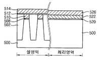
본 발명의 일 실시예에 따르면, 상기 마스크 패턴은 페리 회로 영역에도 함께 형성되고, 상기 페리 회로 영역에 형성되는 마스크 패턴은 상기 희생 마스크 패턴보다 넓은 폭을 가질 수 있다.According to an embodiment of the present invention, the mask pattern is also formed in the ferrier circuit region, and the mask pattern formed in the ferrier circuit region may have a wider width than the sacrificial mask pattern.
본 발명의 일 실시예에 따르면, 상기 희생 마스크 패턴, 제1 갭 및 제1 스페이서 패턴의 폭이 각각 F일 때 상기 마스크 패턴은 절단 부위 내의 정 위치에서 수평 방향으로의 미스 얼라인 마진이 1.5F일 수 있다.According to an embodiment of the present invention, when the widths of the sacrificial mask pattern, the first gap, and the first spacer pattern are F, the mask pattern has a misalignment margin in a horizontal direction at a predetermined position in a cut- Lt; / RTI >
본 발명의 일 실시예에 따르면, 상기 갭필막은 금속을 포함할 수 있다.According to an embodiment of the present invention, the gap fill film may include a metal.
본 발명의 일 실시예에 따르면, 상기 제1 라인 패턴은 신호 전달용 라인일 수 있다.According to an embodiment of the present invention, the first line pattern may be a signal transmission line.
본 발명의 일 실시예에 따르면, 상기 제1 라인 패턴은 홀수개이고, 상기 희생 마스크 패턴에 의해 상기 제1 갭들이 끊어지도록, 상기 희생 마스크 패턴은 수평 방향으로 서로 연결된 H자 형상을 가질 수 있다.According to an embodiment of the present invention, the first line pattern is an odd number, and the sacrificial mask pattern may have an H-shape connected to each other in the horizontal direction so that the first gaps are broken by the sacrificial mask pattern.
이 경우, 상기 마스크 패턴은 상기 각각의 고립된 제1 갭들을 서로 연결시키는 하나의 라인 형상을 가질 수 있다.In this case, the mask pattern may have a single line shape connecting the respective isolated first gaps to each other.
본 발명의 일 실시예에 따르면, 상기 제1 라인 패턴은 홀수개이고, 상기 제1 갭이 수평 방향으로 서로 연결된 H자 형상을 갖도록 상기 희생 마스크 패턴은 끊어진 라인 형상을 갖도록 형성될 수 있다.According to an embodiment of the present invention, the sacrificial mask pattern may be formed to have a broken line shape so that the first line pattern is an odd number, and the first gap has an H shape connected to each other in the horizontal direction.
이 경우, 상기 마스크 패턴은 상기 희생 마스크 패턴의 끊어진 부위를 서로 연결시키는 하나의 라인 형상을 가질 수 있다.In this case, the mask pattern may have a line shape connecting the broken portions of the sacrificial mask pattern to each other.
상기한 목적을 달성하기 위한 본 발명의 다른 실시예에 따른 라인 패턴 구조물의 형성 방법으로, 기판에 형성된 식각 대상막 상에 고립된 패턴 형상의 예비 하드 마스크 패턴을 형성한다. 상기 예비 하드 마스크 패턴 및 식각 대상막 상에, 상기 예비 하드 마스크 패턴의 적어도 일부분과 겹치면서 서로 평행한 복수의 희생 라인들 및 상기 희생 라인들을 서로 수평 연결하는 연결 라인을 포함하는 희생 마스크 패턴을 형성한다. 상기 희생 마스크 패턴 표면 및 식각 대상막 상에 스페이서막을 형성한다. 상기 스페이서막 및 하부에 노출된 예비 하드 마스크 패턴을 이방성 식각하여, 하드 마스크 패턴 및 상기 희생 마스크 패턴들과의 사이에 제1 갭이 생성되면서 상기 희생 마스크 패턴 측벽에 제1 스페이서 패턴들을 형성한다. 상기 희생 마스크 패턴을 제거한다. 상기 제1 스페이서 패턴 및 하드 마스크 패턴을 이용하여 상기 식각 대상막을 식각하여, 절단된 라인 형상을 포함하는 트렌치들을 형성한다. 또한, 상기 트렌치들 내부에 갭필용 물질을 채워넣어, 특정 영역에서 끊어진 라인 형상을 갖는 적어도 하나의 제1 라인 패턴을 형성한다.According to another aspect of the present invention, there is provided a method of forming a line pattern structure, including forming a patterned preliminary hard mask pattern on an etch target film formed on a substrate. Forming a sacrificial mask pattern on the preliminary hard mask pattern and the etch target film, the sacrificial mask pattern including a plurality of sacrificial lines that are parallel to each other and overlap the at least a portion of the preliminary hard mask pattern and a connecting line horizontally connecting the sacrificial lines to each other . A spacer film is formed on the sacrificial mask pattern surface and the etching target film. Anisotropically etching the spacer film and the preliminary hard mask pattern exposed at the lower portion to form first spacer patterns on the side walls of the sacrificial mask pattern while generating a first gap between the hard mask pattern and the sacrificial mask patterns. The sacrificial mask pattern is removed. The etch target film is etched using the first spacer pattern and the hard mask pattern to form trenches including the cut line shape. In addition, a gap filling material is filled in the trenches to form at least one first line pattern having a broken line shape in a specific region.
본 발명의 일 실시예에 따르면, 상기 예비 하드 마스크 패턴은 실리콘 질화물로 형성할 수 있다.According to an embodiment of the present invention, the preliminary hard mask pattern may be formed of silicon nitride.
본 발명의 일 실시예에 따르면, 상기 희생 마스크 패턴, 제1 갭 및 제1 스페이서 패턴의 폭이 각각 F일 때 상기 하드 마스크 패턴은 절단 부위 내의 정 위치로부터 수평 방향으로의 미스 얼라인 마진이 1.5F일 수 있다.According to an embodiment of the present invention, when the widths of the sacrificial mask pattern, the first gap, and the first spacer pattern are F, the misalignment margin in the horizontal direction from the fixed position in the cut portion is 1.5 F < / RTI >
설명한 것과 같이, 본 발명에 따르면 라인 패턴 구조물을 형성할 때, 희생 마스크 패턴의 구조를 변경하여 끊어지는 부위의 희생 마스크 패턴 및 갭 부위의 일부가 이미 끊겨진 형상을 갖도록 한다. 그러므로, 라인 패턴 구조물에 포함된 라인을 끊어내기 위한 마스크 패턴의 형성 부위가 감소되며, 이로인해 상기 마스크 패턴의 미스 얼라인 마진이 증가된다. 이와같이, 미스 얼라인 마진이 증가됨으로써, 상기 미스 얼라인에 의해 목표한 라인이 끊어지지 않거나 또는 끊기지 않고 연장되어야 하는 이웃 라인이 끊어지거나 선폭이 감소되는 등의 불량이 감소된다. 또한, 상기 라인 패턴 구조물을 형성하는데 요구되는 공정 스텝이 감소된다. 따라서, 상기 라인 패턴 구조물이 포함되는 반도체 소자의 불량이 감소되며, 반도체 소자의 양산성을 높힐 수 있다.As described above, according to the present invention, when the line pattern structure is formed, the structure of the sacrificial mask pattern is changed so that the sacrificial mask pattern at the cut-off portion and a part of the gap portion are already broken. Therefore, the formation region of the mask pattern for breaking the lines included in the line pattern structure is reduced, thereby increasing the misalignment margin of the mask pattern. In this way, the increase in misalignment margin reduces the defects such as the breakage of the target line by the misalignment, the breakage of the neighboring line which is to be extended without breaking, or the reduction of the line width. Also, the process steps required to form the line pattern structure are reduced. Therefore, defects of the semiconductor device including the line pattern structure are reduced, and the mass productivity of the semiconductor device can be enhanced.
도 1은 본 발명의 실시예 1에 따른 패턴 구조물을 나타내는 단면도이다.
도 2a 내지 도 2f는 도 1에 도시된 패턴 구조물의 형성 방법을 나타내는 평면도들이다.
도 3a 내지 도 3f는 도 1에 도시된 패턴 구조물의 형성 방법을 나타내는 단면도들이다.
도 4a 내지 도 4c는 마스크 패턴이 좌로 1.5F 미스 얼라인되었을 때의 패턴 구조물 형성 방법을 나타내는 단면도들이다.
도 5a 내지 도 5c는 마스크 패턴이 우로 1.5F 미스 얼라인되었을 때의 패턴 구조물 형성 방법을 나타내는 단면도들이다.
도 6a 내지 6c는 본 발명의 일 실시예에 따른 패턴 구조물의 형성 방법을 나타내는 평면도들이다.
도 7a 내지 7d는 본 발명의 실시예 2에 따른 패턴 구조물의 형성 방법을 나타내는 평면도들이다.
도 8a 내지 8d는 본 발명의 실시예 3에 따른 패턴 구조물의 형성 방법을 나타내는 평면도들이다.
도 9a 내지 9d는 본 발명의 실시예 4에 따른 패턴 구조물의 형성 방법을 나타내는 평면도들이다.
도 10a 내지 10d는 본 발명의 실시예 5에 따른 패턴 구조물의 형성 방법을 나타내는 평면도들이다.
도 11a 내지 도 11e는 본 발명의 실시예 6에 따른 패턴 구조물의 형성 방법을 나타내는 평면도들이다.
도 12a 내지 도 12f는 도 11e에 도시된 패턴 구조물의 형성 방법을 나타내는 단면도들이다.
도 13a 내지 13d는 본 발명의 일 실시예에 따른 패턴 구조물의 형성 방법을 나타내는 평면도들이다.
도 14a 내지 14d는 본 발명의 실시예 7에 따른 패턴 구조물의 형성 방법을 나타내는 평면도들이다.
도 15a 내지 15d는 본 발명의 실시예 8에 따른 패턴 구조물의 형성 방법을 나타내는 평면도들이다.
도 16a 내지 16d는 본 발명의 실시예 9에 따른 패턴 구조물의 형성 방법을 나타내는 평면도들이다.
도 17a 내지 17d는 본 발명의 실시예 10에 따른 패턴 구조물의 형성 방법을 나타내는 평면도들이다.
도 18a 내지 도 18c는 본 발명의 실시예 11에 따른 패턴 구조물의 형성 방법을 나타내는 평면도들이다.
도 19a 내지 도 19c는 도 18c에 도시된 패턴 구조물의 형성 방법을 나타내는 단면도들이다.
도 20a 내지 도 20c는 본 발명의 실시예 12에 따른 패턴 구조물의 형성 방법을 나타내는 평면도들이다.
도 21a 내지 도 21c는 도 20c에 도시된 패턴 구조물의 형성 방법을 나타내는 단면도들이다.
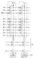
도 22는 본 발명의 실시예 13에 따른 플래시 메모리 소자의 회로도이다.
도 23은 플래시 메모리 소자에서 비트 라인 단부의 레이아웃이다.
도 24a 내지 도 24e는 본 발명의 실시예 13에 따른 플래시 메모리 소자의 제조 방법을 나타내는 단면도들이다.
도 25는 본 발명의 실시예에 따른 정보 처리 시스템을 간략히 보여주는 블록도이다.1 is a cross-sectional view showing a pattern structure according to a first embodiment of the present invention.
FIGS. 2A to 2F are plan views showing a method of forming the pattern structure shown in FIG.
3A to 3F are cross-sectional views illustrating a method of forming the pattern structure shown in FIG.
4A to 4C are cross-sectional views showing a method of forming a pattern structure when the mask pattern is misaligned to the left by 1.5F.
FIGS. 5A to 5C are cross-sectional views showing a method of forming a pattern structure when the mask pattern is misaligned to 1.5 F. FIG.
6A to 6C are plan views illustrating a method of forming a pattern structure according to an embodiment of the present invention.
7A to 7D are plan views showing a method of forming a pattern structure according to a second embodiment of the present invention.
8A to 8D are plan views illustrating a method of forming a pattern structure according to a third embodiment of the present invention.
9A to 9D are plan views showing a method of forming a pattern structure according to a fourth embodiment of the present invention.
10A to 10D are plan views showing a method of forming a pattern structure according to a fifth embodiment of the present invention.
11A to 11E are plan views showing a method of forming a pattern structure according to a sixth embodiment of the present invention.
12A to 12F are cross-sectional views illustrating a method of forming the pattern structure shown in FIG. 11E.
13A to 13D are plan views illustrating a method of forming a pattern structure according to an embodiment of the present invention.
14A to 14D are plan views showing a method of forming a pattern structure according to a seventh embodiment of the present invention.
15A to 15D are plan views showing a method of forming a pattern structure according to an eighth embodiment of the present invention.
16A to 16D are plan views showing a method of forming a pattern structure according to a ninth embodiment of the present invention.
17A to 17D are plan views showing a method of forming a pattern structure according to a tenth embodiment of the present invention.
18A to 18C are plan views showing a method of forming a pattern structure according to an eleventh embodiment of the present invention.
Figs. 19A to 19C are cross-sectional views showing a method of forming the pattern structure shown in Fig. 18C.
20A to 20C are plan views showing a method of forming a pattern structure according to a twelfth embodiment of the present invention.
Figs. 21A to 21C are cross-sectional views showing a method of forming the pattern structure shown in Fig. 20C.
22 is a circuit diagram of a flash memory device according to a thirteenth embodiment of the present invention.
23 is a layout of bit line ends in a flash memory device.
24A to 24E are cross-sectional views illustrating a method of manufacturing a flash memory device according to a thirteenth embodiment of the present invention.
25 is a block diagram briefly showing an information processing system according to an embodiment of the present invention.
이하, 첨부한 도면을 참조하여 본 발명의 바람직한 실시예를 상세히 설명하고자 한다.Hereinafter, preferred embodiments of the present invention will be described in detail with reference to the accompanying drawings.
본 발명의 각 도면에 있어서, 구조물들의 치수는 본 발명의 명확성을 기하기 위하여 실제보다 확대하여 도시한 것이다.In the drawings of the present invention, the dimensions of the structures are enlarged to illustrate the present invention in order to clarify the present invention.
본 발명에서, 제1, 제2 등의 용어는 다양한 구성요소들을 설명하는데 사용될 수 있지만, 상기 구성요소들은 상기 용어들에 의해 한정되어서는 안 된다. 상기 용어들은 하나의 구성요소를 다른 구성요소로부터 구별하는 목적으로만 사용된다.In the present invention, the terms first, second, etc. may be used to describe various elements, but the elements should not be limited by the terms. The terms are used only for the purpose of distinguishing one component from another.
본 발명에서 사용한 용어는 단지 특정한 실시예를 설명하기 위해 사용된 것으로, 본 발명을 한정하려는 의도가 아니다. 단수의 표현은 문맥상 명백하게 다르게 뜻하지 않는 한, 복수의 표현을 포함한다. 본 출원에서, "포함하다" 또는 "가지다" 등의 용어는 명세서 상에 기재된 특징, 숫자, 단계, 동작, 구성요소, 부품 또는 이들을 조합한 것이 존재함을 지정하려는 것이지, 하나 또는 그 이상의 다른 특징들이나 숫자, 단계, 동작, 구성요소, 부품 또는 이들을 조합한 것들의 존재 또는 부가 가능성을 미리 배제하지 않는 것으로 이해되어야 한다.The terminology used herein is for the purpose of describing particular embodiments only and is not intended to be limiting of the invention. The singular expressions include plural expressions unless the context clearly dictates otherwise. In the present application, the terms "comprises" or "having" and the like are used to specify that there is a feature, a number, a step, an operation, an element, a component or a combination thereof described in the specification, But do not preclude the presence or addition of one or more other features, integers, steps, operations, elements, components, or combinations thereof.
본 발명에 있어서, 각 층(막), 영역, 전극, 패턴 또는 구조물들이 대상체, 기판, 각 층(막), 영역, 전극 또는 패턴들의 "상에", "상부에" 또는 "하부"에 형성되는 것으로 언급되는 경우에는 각 층(막), 영역, 전극, 패턴 또는 구조물들이 직접 기판, 각 층(막), 영역, 또는 패턴들 위에 형성되거나 아래에 위치하는 것을 의미하거나, 다른 층(막), 다른 영역, 다른 전극, 다른 패턴 또는 다른 구조물들이 대상체나 기판 상에 추가적으로 형성될 수 있다.In the present invention, it is to be understood that each layer (film), region, electrode, pattern or structure may be formed on, over, or under the object, substrate, layer, Means that each layer (film), region, electrode, pattern or structure is directly formed or positioned below a substrate, each layer (film), region, or pattern, , Other regions, other electrodes, other patterns, or other structures may additionally be formed on the object or substrate.
본문에 개시되어 있는 본 발명의 실시예들에 대해서, 특정한 구조적 내지 기능적 설명들은 단지 본 발명의 실시예를 설명하기 위한 목적으로 예시된 것으로, 본 발명의 실시예들은 다양한 형태로 실시될 수 있으며 본문에 설명된 실시예들에 한정되는 것으로 해석되어서는 안된다.For the embodiments of the invention disclosed herein, specific structural and functional descriptions are set forth for the purpose of describing an embodiment of the invention only, and it is to be understood that the embodiments of the invention may be practiced in various forms, But should not be construed as limited to the embodiments set forth in the claims.
즉, 본 발명은 다양한 변경을 가할 수 있고 여러 가지 형태를 가질 수 있는 바, 특정 실시예들을 도면에 예시하고 본문에 상세하게 설명하고자 한다. 그러나, 이는 본 발명을 특정한 개시 형태에 대해 한정하려는 것이 아니며, 본 발명의 사상 및 기술 범위에 포함되는 모든 변경, 균등물 내지 대체물을 포함하는 것으로 이해되어야 한다.
That is, the present invention is capable of various modifications and various forms, and specific embodiments are illustrated in the drawings and described in detail in the following description. It should be understood, however, that the invention is not intended to be limited to the particular forms disclosed, but includes all modifications, equivalents, and alternatives falling within the spirit and scope of the invention.
실시예 1Example 1
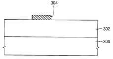
도 1은 본 발명의 실시예 1에 따른 패턴 구조물을 나타내는 단면도이다.1 is a cross-sectional view showing a pattern structure according to a first embodiment of the present invention.
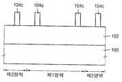
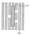
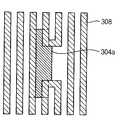
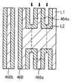
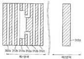
도 1을 참조하면, 제1 영역 및 제2 영역이 구분되는 기판(100)이 구비된다. 상기 기판(100)의 제1 영역은 끊어진 제1 라인 패턴(114a)들 및 끊어진 라인들 양 측과 이웃하는 제2 라인 패턴(114b)들이 형성되는 영역이다. 또한, 상기 제2 영역은 제1 영역 이외의 나머지 영역으로 라인 및 스페이스가 반복되는 제3 라인 패턴(114c)들이 형성되는 영역이다.Referring to FIG. 1, the
본 실시예에서, 상기 제1 영역에는 끊어진 부위를 포함하는 라인 형상을 갖는 2개의 제1 라인 패턴(114a)이 구비된다. 이하에서, 제1 방향으로 나란하게 연장되는 끊어진 부분을 포함하는 라인은 1개의 제1 라인 패턴(114a)이라 하면서 설명한다. 상기 제1 라인 패턴(114a)이 끊어지는 부위와 인접해서는 상기 제1 라인 패턴(114a)의 선폭이 다소 감소될 수 있다.In the present embodiment, the first region is provided with two
상기 제1 영역에서, 상기 제1 라인 패턴(114a)들 양 측에 이웃하여 끊어진 부위가 없는 제2 라인 패턴(114b)이 각각 구비된다. 상기 제2 라인 패턴(114b)은 상기 제1 라인 패턴(114a) 외곽에 각각 1개씩 구비되므로, 모두 2개가 구비된다. 상기 제2 라인 패턴(114b)은 상기 제1 라인 패턴(114a)과 평행하게 상기 제1 방향으로 연장되는 연장 라인(L3)과, 상기 제1 라인 패턴(114a)의 끊어진 부위와 인접하는 영역에서 상기 제1 라인 패턴(114a)으로 향하도록 상기 연장 라인(L3)으로부터 측방 돌출된 적어도 하나의 돌출 패턴(L4)을 포함한다. 상기 돌출 패턴(L4)은 상기 연장 라인(L3) 이외에 다른 이웃하는 패턴들과 접촉되지 않는다. 상기 돌출 패턴(L4)은 상기 제1 라인 패턴(114a)을 향해 돌출된다. 또한, 2개의 제2 라인 패턴(114b)들 각각에 포함되는 돌출 패턴(L4)은 서로 다른 위치에 위치할 수 있다. 그러므로, 상기 각각의 제2 라인 패턴(114b)들은 서로 다른 형상을 가질 수 있다.In the first region,
상기 각각의 제2 라인 패턴(114b)에는 동일한 개수의 돌출 패턴(L4)이 포함될 수도 있고, 다른 개수의 돌출 패턴(L4)이 포함될 수도 있다. 본 실시예에서, 상기 제2 라인 패턴(114b) 중 좌측 제2 라인 패턴은 2개의 돌출 패턴(L4)이 포함되고, 우측 제2 라인 패턴은 1개의 돌출 패턴(L4)이 포함된다.The same number of protruding patterns L4 may be included in each
상기 제2 라인 패턴(114b)의 외곽의 제2 영역에는, 상기 제2 라인 패턴(114b)과 평행하는 제3 라인 패턴(114c)들이 더 구비된다. 상기 제3 라인 패턴(114c)들은 끊어진 부위없이 라인 및 스페이스가 반복되는 형상을 갖는다. 상기 제3 라인 패턴(114c)에 포함되는 각 라인들은 일방향으로 연속적으로 연장되는 형상을 갖는다. 즉, 상기 제3 라인 패턴(114c)은 돌출 패턴이 구비되지 않는다.
상기 제1 라인 패턴(114a)이 절단된 부위 이외의 영역에서 상기 제1 내지 제3 라인 패턴(114a~114c)의 선폭은 모두 동일할 수 있다. 또한, 각 라인 패턴들의 간격(114a~114c)은 상기 제1 내지 제3 라인 패턴(114a~114c)의 선폭과 동일할 수 있다.The line widths of the first to
상기 제1 라인 패턴(114a)들의 끊어진 부위에는 고립된 형태의 더미 패턴(116)이 더 구비될 수도 있다.The
상기 제1 내지 제3 라인 패턴들과 더미 패턴들 사이에는 식각 대상막 패턴(102a)이 구비된다. 상기 식각 대상막 패턴(102a)은 절연 물질 또는 반도체 물질을 포함할 수 있다.A film pattern to be etched 102a is provided between the first to third line patterns and the dummy patterns. The etching
상기 제1 내지 제3 라인 패턴(114a~114c) 및 더미 패턴(116)을 포함하는 패턴 구조물은 도전 물질을 포함할 수 있다. 이 경우, 상기 패턴 구조물은 신호 전달을 위한 라인, 예를들어 비트 라인, 워드 라인 등으로 사용될 수 있다.The pattern structure including the first to
이와는 달리, 상기 패턴 구조물은 절연 물질을 포함할 수 있다. 이 경우, 상기 패턴 구조물은 소자 분리막 패턴으로 사용될 수 있다.
Alternatively, the pattern structure may comprise an insulating material. In this case, the pattern structure may be used as a device isolation film pattern.
도 2a 내지 도 2f는 도 1에 도시된 패턴 구조물의 형성 방법을 나타내는 평면도들이다. 도 3a 내지 도 3f는 도 1에 도시된 패턴 구조물의 형성 방법을 나타내는 단면도들이다. 도 3a 내지 도 3f는 도 2a의 I'I'부위를 절단하였을 때 보여지는 단면도들이다.FIGS. 2A to 2F are plan views showing a method of forming the pattern structure shown in FIG. 3A to 3F are cross-sectional views illustrating a method of forming the pattern structure shown in FIG. Figs. 3A to 3F are cross-sectional views of the portion I'I 'shown in Fig. 2A when cut.
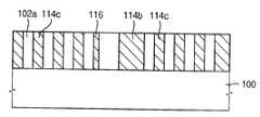
도 2a 및 도 3a를 참조하면, 제1 영역 및 제2 영역이 구분되는 기판(100)을 마련한다. 상기 기판(100)의 제1 영역은 끊어진 라인들 및 끊어진 라인들 양 측의 이웃하는 하나의 라인이 형성되기 위한 영역이다. 또한, 상기 기판(100)의 제2 영역은 제1 영역 이외의 나머지 영역으로 라인 및 스페이스(line and space)가 반복 형성되기 위한 영역이다.Referring to FIGS. 2A and 3A, the
상기 기판(100) 상에 식각 대상막(102)을 형성한다. 상기 식각 대상막(102)은 실리콘 산화물 또는 실리콘 질화물과 같은 절연막일 수 있다. 이와는 다른 예로, 상기 식각 대상막(102)이 별도로 형성되지 않고, 기판(100) 자체가 식각 대상물이 될 수도 있다.A film to be etched 102 is formed on the
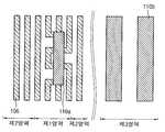
상기 식각 대상막(102) 상에 희생 마스크막(도시안함)을 형성한다. 상기 희생 마스크막은 단일층으로 형성할 수도 있고, 2 층 이상의 적층 구조를 가질 수도 있다. 상기 희생 마스크막은 스핀 코팅으로 형성될 수 있는 반사 방지막 및 포토레지스트막일 수 있다. 상기 희생 마스크막을 패터닝함으로써, 제1 내지 제3 희생 마스크 패턴(104a, 104b, 104c)을 각각 형성한다.A sacrificial mask film (not shown) is formed on the
상기 제1 및 제2 희생 마스크 패턴(104a, 104b)은 제1 영역의 기판(100) 상에 형성되며, 끊어진 제1 라인 패턴 및 끊어진 제1 라인 패턴과 이웃하는 제2 라인 패턴을 형성하기 위한 것이다. 또한, 상기 제3 희생 마스크 패턴(104c)은 제2 영역의 기판(100)상에 형성되며, 끊어지지 않고 연장되는 제3 라인 패턴들을 형성하기 위한 것이다.The first and second
도시하지는 않았지만, 상기 제3 희생 마스크 패턴(104c)은 라인 및 스페이스가 반복되는 형태로 배치된다. 이 때, 최종적으로 형성하고자 하는 제3 라인 패턴의 선폭을 F라고 하면, 상기 제3 희생 마스크 패턴(104c)의 선폭은 F이고, 상기 제3 희생 마스크 패턴들(104c)의 간격은 3F가 되도록 한다.Although not shown, the third
한편, 상기 제1 및 제2 희생 마스크 패턴(104a, 104b)은 끊어지는 라인 패턴의 개수에 따라 다른 형상을 가질 수 있다.Meanwhile, the first and second
본 실시예에서는, 2개의 끊어진 제1 라인 패턴 및 제1 라인 패턴과 이웃하는 제2 라인 패턴을 형성한다. 이를 위하여 2개의 서로 다른 형상을 갖는 제1 및 제2 희생 마스크 패턴(104a, 104b)을 형성한다. 제1 희생 마스크 패턴(104a)은 상기 제3 희생 마스크 패턴(104c)과 동일하게 끊어지는 부분없이 연장되는 라인 형상을 갖는다. 그러나, 상기 제2 희생 마스크 패턴(104b)은 끊어진 연장 라인(L1)을 포함하고, 상기 연장 라인(L1)이 끊어지는 부위는 형성하고자 하는 제1 라인 패턴이 끊어지는 부위에 해당된다. 또한, 상기 제2 희생 마스크 패턴(104b)은 상기 연장 라인(L1)의 끊어진 부위로부터 이웃하는 제1 희생 마스크 패턴(104a)으로 수평 연결되는 연결 라인(L2)을 포함한다. 즉, 상기 제1 희생 마스크 패턴(104a) 및 상기 제1 희생 마스크 패턴(104a)과 연결된 상기 제2 희생 마스크 패턴(104b)은 연결 부위에서 π자 형상을 갖는다. 상기 제2 희생 마스크 패턴(104b)은 상기 제1 희생 마스크 패턴(104a)의 우측에 구비된다.In this embodiment, two broken first line patterns and a first line pattern and a neighboring second line pattern are formed. For this purpose, first and second
상기 제2 희생 마스크 패턴(104b)의 연장 라인(L1)과 상기 연장 라인(L1)과 이웃하는 제1 희생 마스크 패턴(104a) 간의 간격은 3F가 되도록 한다. 상기 제2 희생 마스크 패턴(104b)의 연장 라인(L1)과 상기 연장 라인(L1)과 이웃하는 제3 희생 마스크 패턴(104c) 간의 간격은 3F가 되도록 한다. 또한, 상기 제3 희생 마스크 패턴(104c)과 제1 희생 마스크 패턴(104a) 간의 간격도 3F가 되도록 한다.The interval between the extension line L1 of the second
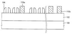
도 2b 및 3b를 참조하면, 상기 제1 내지 제3 희생 마스크 패턴(104a~104c)과 상기 식각 대상막(102) 표면을 따라 스페이서막(도시안함)을 형성한다. 상기 스페이서막은 상기 제1 내지 제3 희생 마스크 패턴(104a~104c)과 다른 식각 특성을 갖는 물질로 이루어질 수 있다. 예를들어, 상기 스페이서막은 실리콘 산화물로 형성될 수 있다. 상기 스페이서막은 균일한 두께를 갖도록 형성하기 위하여 ALD (atomic layer deposition) 공정을 이용할 수 있다.Referring to FIGS. 2B and 3B, a spacer film (not shown) is formed along the surfaces of the first to third
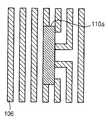
상기 스페이서막을 에치백하여 상기 제1 내지 제3 희생 마스크 패턴(104a~104c)의 측벽에는 각각 스페이서 패턴(106)을 형성한다. 이 때, 상기 스페이서 패턴들(106) 사이에는 갭(108)들이 생성된다. 이 때, 상기 스페이서 패턴(106)의 선폭과 상기 갭(108)들의 폭은 F일 수 있다. 여기서, 상기 갭(108)들과 상기 제1 내지 제3 희생 마스크 패턴(104a~104c)이 형성되어 있는 부위는 상기 제1 내지 제3 라인 패턴의 형성 영역이 된다.The spacer film is etched back to
설명한 것과 같이, 본 실시예에서, 상기 제2 희생 마스크 패턴(104b)은 절단된 형태의 연장 라인(L1) 및 연장 라인(L1)의 절단된 단부와 제1 희생 마스크 패턴(104a)을 연결하는 연결 라인(L2)을 포함한다. 그러므로, 상기 제2 희생 마스크 패턴(104b)과 이웃하는 제1 희생 마스크 패턴(104a) 사이에 생성되는 제1 갭(108a)이 끊겨진 라인 형상을 갖게된다. 즉, 상기 제2 희생 마스크 패턴(104b)의 연결 라인(L2)에 의해서, 상기 제1 갭(108a)이 미리 분리되어 있는 형상을 갖게된다. 또한, 상기 제2 희생 마스크 패턴(104b)과 이웃하는 제3 희생 마스크 패턴(104c) 사이에 생성되는 제2 갭(108b)은 라인 형상을 가지면서 연장되고, 상기 라인의 일부 영역에서 측방으로 돌출되는 형상을 갖게된다. 반면에, 나머지 스페이서 패턴들(106) 사이에 위치하는 제3 갭(108c)은 끊겨지는 부위없이 연장되는 라인 형상을 갖는다.As described, in the present embodiment, the second
도 2c 및 3c를 참조하면, 상기 식각 대상막(102) 상에 상기 스페이서 패턴(106)들 및 희생 마스크 패턴들(104a~104c)을 덮는 마스크막(도시안함)을 형성한다. 상기 마스크막은 스핀 코팅에 의해 형성될 수 있는 막일 수 있다. 예를들어, 상기 마스크막은 스핀 온 하드 마스크막(SOH) 또는 포토레지스트막일 수 있다. 상기 마스크막은 실리콘 산화물 또는 질화물과 같은 증착에 의해 형성되는 하드 마스크막을 사용하지 않아도 된다. 그러므로, 상기 마스크막을 형성하는 공정이 매우 간단하다.2C and 3C, a mask film (not shown) is formed on the
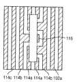
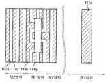
상기 마스크막을 사진공정에 의해 패터닝함으로써 상기 기판(100)의 제1 영역에 마스크 패턴(110)을 형성한다. 상기 마스크 패턴(110)은 끊어진 제1 라인 패턴 및 상기 제1 라인 패턴과 이웃하는 제2 라인 패턴을 형성하기 위하여 제공된다.A
상기 마스크 패턴(110)은 서로 평행하게 배치되는 2개의 연결 라인(L2)을 수직 방향으로 연결시키는 라인 형상을 갖는다. 이 때, 상기 마스크 패턴(110)은 상기 제1 희생 마스크 패턴(104a) 상부를 덮지 않도록 형성되어야 한다. 상기 제1 갭(108a)은 상기 제2 희생 마스크 패턴(104b)에 의해 이미 분리가 되어 있으나, 상기 제2 희생 마스크 패턴(104b)은 상기 연결 라인(L2)에 의해 이웃하는 제1 희생 마스크 패턴(104a)과 접촉되어 있다. 그러므로, 상기 마스크 패턴(110)을 사용하여 상기 연결 라인(L2)이 분리되도록 하여야 한다.The
상기 마스크 패턴(110)은 2F의 폭을 가질 수 있으며, 길이 방향으로 상기 제1 갭(108a)까지 연장되는 형상을 가질 수 있다. 또한, 상기 마스크 패턴(110)이 정 얼라인 되어 있는 경우, 도시된 것과 같이, 상기 마스크 패턴(110)의 좌측벽으로부터 상기 제1 희생 마스크 패턴까지가 1.5F만큼 이격되어 있다.The
그러나, 상기 마스크 패턴(110)은 정 얼라인되었을 때를 기준으로 좌, 우 1.5F까지 미스 얼라인이 발생하더라도 최종적으로 형성되는 제1 라인 패턴은 상기 마스크 패턴(110)의 형성 영역에서 서로 끊어진 형상을 가질 수 있다. 즉, 상기 마스크 패턴은 좌, 우 1.5F의 미스 얼라인 마진을 갖는다.However, even if misalignment occurs to the left and right 1.5F with respect to the case where the
도 2d 및 3d를 참조하면, 상기 제1 내지 제3 희생 마스크 패턴(104a~104c)을 제거한다. 이 때, 상기 마스크 패턴(110)에 의해 덮혀있는 제1 내지 제3 희생 마스크 패턴(104a~104c)은 제거되지 않는다.Referring to FIGS. 2D and 3D, the first to third
상기 공정에 의해 남아있는 스페이서 패턴(106)들과 마스크 패턴(110)은 상기 식각 대상막을 식각하기 위한 실질적인 식각 마스크의 역할을 한다. 본 실시예에서는 다마신 방식으로 패턴 구조물을 형성하므로, 스페이서 패턴들(106) 사이에 노출되어 있는 상기 식각 대상막(102)부위에 패턴 구조물이 형성된다. 즉, 상기 제1 내지 제3 희생 마스크 패턴(104a~104c)이 제거된 부위와, 상기 마스크 패턴(110)으로 덮혀있지 않은 제1 내지 제3 갭 부위(108a~108c)에 패턴 구조물이 형성된다.The remaining
도 2e 및 도 3e를 참조하면, 상기 스페이서 패턴들(106)과 마스크 패턴(110)을 식각 마스크로 사용하여 상기 식각 대상막(102)을 식각함으로써, 개구부(112)들을 포함하는 식각 대상막 패턴(102a)을 형성한다.2E and 3E, the
도 2f 및 도 3f를 참조하면, 상기 개구부(112)들 내부를 채우는 매립막(도시안함)을 형성한다. 이 후, 상기 식각 대상막 패턴(102a)의 상부면이 노출되도록 상기 매립막을 연마함으로써 패턴 구조물(114)을 형성한다.Referring to FIGS. 2F and 3F, a buried layer (not shown) filling the
상기 매립막은 도전 물질을 포함할 수 있다. 즉, 상기 매립막은 통상적인 사진 식각 공정을 통해 식각되기 어려운 금속 물질을 포함할 수 있다. 예를들어, 상기 매립막은 구리를 포함할 수 있다.The buried film may include a conductive material. That is, the buried layer may include a metal material that is difficult to etch through a conventional photolithography process. For example, the embedding film may comprise copper.
이와는 다른 예로, 상기 매립막은 절연 물질을 포함할 수 있다. 상기 개구부 내에 절연 물질이 매립됨으로써, 소자 분리용 패턴이 형성될 수 있다. 이와는 다른 예로, 상기 매립막을 형성하지 않고, 상기 식각 대상막 패턴을 하드 마스크로 사용하여, 하부에 형성된 막을 식각할 수도 있다.As another example, the buried film may include an insulating material. An insulating material is buried in the opening, so that a device isolation pattern can be formed. As another example, the film formed below may be etched using the etching target film pattern as a hard mask without forming the buried film.
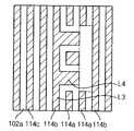
상기 공정을 수행하여 형성되는 패턴 구조물(114)은 끊겨진 부위를 갖는 제1 라인 패턴(114a)들과, 상기 제1 라인 패턴(114a) 양 측에 각각 하나씩 배치되는 제2 라인 패턴(114b)들 및 상기 제2 라인 패턴 외곽으로 배치되는 제3 라인 패턴(114c)들을 포함한다.The pattern structure 114 formed by performing the above process includes a
상기 제1 라인 패턴(114a)은 2개가 구비된다. 상기 제2 라인 패턴(114b)은 제1 라인 패턴(114a)과 동일한 방향으로 연장되고 끊겨진 부위가 없는 연장 라인(L3)과, 상기 연장 라인(L3)으로부터 제1 라인 패턴(114a)으로 향하는 방향으로 측방 돌출되는 돌출 패턴(L4)을 포함한다. 상기 돌출 패턴(L4)은 상기 제1 라인 패턴(114a)의 끊겨진 부위와 인접하게 배치된다. 이 때, 상기 돌출 패턴은 얼라인 마진을 충분하게 하도록 하기 위하여 제2 희생 마스크 패턴(104b)에 연결 라인(L2)이 구비됨으로써 생성되는 것이다. 상기 제3 라인 패턴(114c)은 라인 및 스페이스가 반복되는 형상을 갖는다.Two of the
또한, 상기 제1 라인 패턴(114a)이 끊겨진 부위에는 고립된 형상의 더미 패턴(116)이 형성될 수 있다.In addition, a
상기에서 설명한 것과 같이, 더블 패터닝 공정을 통해 끊겨진 부위를 포함하는 미세 라인 패턴을 형성하는데 있어서, 상기 끊겨진 부위를 형성하기 위한 마스크 패턴의 미스 얼라인 마진이 1.5F로 증가된다. 그러므로, 상기 마스크 패턴의 미스 얼라인에 의해 상기 미세 라인 패턴이 끊어지지 않거나 또는 연장되어야 하는 라인이 끊어지는 등의 불량이 감소된다.
As described above, in forming the fine line pattern including the broken portion through the double patterning process, the misalignment margin of the mask pattern for forming the broken portion is increased to 1.5F. Therefore, defects such as breakage of the fine line pattern due to misalignment of the mask pattern or breaking of lines to be extended are reduced.
상기 도 2a 내지 도 2f의 방법으로 패턴 구조물을 형성하는 과정에서, 상기 마스크 패턴이 정 위치에 위치하지 못하고 미스 얼라인이 발생될 수 있다. 상기 도 2c에서 설명한 것과 같이, 상기 마스크 패턴이 좌, 우 1.5F까지 미스 얼라인되더라도 완성된 상기 제1 라인 패턴은 절단된 형상을 갖고, 제2 및 제3 라인 패턴이 정상적인 동작을 할 수 있다. 또한, 상기 제2 라인 패턴 중 적어도 하나는 돌출 패턴을 포함하는 형상을 갖는다.In the process of forming the pattern structure according to the method of FIGS. 2A to 2F, the mask pattern may not be located at a predetermined position and misalignment may occur. As described in FIG. 2C, even if the mask pattern is misaligned to the left and right 1.5F, the completed first line pattern has a cut shape, and the second and third line patterns can perform a normal operation . Also, at least one of the second line patterns has a shape including a protruding pattern.
도 4a 내지 도 4c는 마스크 패턴이 좌로 1.5F 미스 얼라인되었을 때의 패턴 구조물 형성 방법을 나타내는 단면도들이다.4A to 4C are cross-sectional views showing a method of forming a pattern structure when the mask pattern is misaligned to the left by 1.5F.
도 4a를 참조하면, 도 2a 및 2b를 참조로 설명한 공정을 수행한 후, 식각 대상막(102) 상에 상기 스페이서 패턴(106)들을 덮는 마스크막(도시안함)을 형성한다. 상기 마스크막을 사진공정에 의해 패터닝함으로써 상기 기판(100)의 제1 영역에 마스크 패턴(110a)을 형성한다.Referring to FIG. 4A, after performing the process described with reference to FIGS. 2A and 2B, a mask film (not shown) covering the
상기 마스크 패턴(110a)은 2F의 폭을 가질 수 있으며, 길이 방향으로는 제1 갭(108a)까지 연장되는 형상을 가질 수 있다. 상기 마스크 패턴(110)의 좌측벽은 상기 제1 희생 마스크 패턴(104a)의 우측벽과 접하게 위치한다.The
도 4b를 참조하면, 상기 제1 내지 제3 희생 마스크 패턴(104a~104c)을 제거한다. 상기 제거 공정은 도 2c를 참조로 설명한 것과 동일하다.Referring to FIG. 4B, the first to third
이 후, 도 2d 내지 도 2f를 참조로 설명한 것과 동일한 공정을 수행함으로써, 도 4c에 도시된 것과 같은 패턴 구조물을 형성한다.Thereafter, by performing the same process as described with reference to Figs. 2D to 2F, a pattern structure as shown in Fig. 4C is formed.
도 4c를 참조하면, 상기 패턴 구조물은 끊겨진 부위를 갖는 라인 형상의 제1 라인 패턴(114a)들이 구비된다. 상기 제1 라인 패턴(114a) 양 측에 각각 하나씩 배치되는 제2 라인 패턴(114b)들 및 상기 제2 라인 패턴 외곽으로 배치되는 제3 라인 패턴(114c)들을 포함한다.Referring to FIG. 4C, the pattern structure is provided with line-shaped
상기 제1 라인 패턴(114a)은 2개가 구비된다. 상기 제1 라인 패턴(114a) 중 하나는 단부에서 마주하는 제1 라인 패턴(114a) 방향으로 꺽여진 형상을 갖는다,Two of the
상기 제2 라인 패턴(114b) 중 우측에 위치하는 것은 제1 라인 패턴(114a)과 동일한 방향으로 연장되고 끊겨진 부위가 없는 연장 라인(L3)과, 상기 연장 라인(L3)으로부터 제1 라인 패턴(114a)으로 향하는 방향으로 측방 돌출되는 돌출 패턴(L4)을 포함한다. 또한, 나머지 제2 라인 패턴(114b)은 돌출 패턴없이 연장되는 라인 형상을 갖는다. 상기 제3 라인 패턴(114c)은 라인 및 스페이스가 반복되는 형상을 갖는다.The right line of the
도 5a 내지 도 5c는 마스크 패턴이 우로 1.5F 미스 얼라인되었을 때의 패턴 구조물 형성 방법을 나타내는 단면도들이다.FIGS. 5A to 5C are cross-sectional views showing a method of forming a pattern structure when the mask pattern is misaligned to 1.5 F. FIG.
도 5a를 참조하면, 도 2a 및 2b를 참조로 설명한 공정을 수행한 후, 식각 대상막(102) 상에 상기 스페이서 패턴(106)들을 덮는 마스크막(도시안함)을 형성한다. 상기 마스크막을 사진공정에 의해 패터닝함으로써 상기 기판(100)의 제1 영역에 마스크 패턴(110b)을 형성한다.Referring to FIG. 5A, after performing the process described with reference to FIGS. 2A and 2B, a mask film (not shown) covering the
상기 마스크 패턴(110b)은 2F의 폭을 가질 수 있으며, 상기 제1 갭까지 연장되는 형상을 가질 수 있다. 상기 마스크 패턴(110b)의 좌측벽은 상기 제2 희생 마스크 패턴(104b)의 연장 라인의 좌측벽과 접하게 위치한다.The
도 5b를 참조하면, 상기 제1 내지 제3 희생 마스크 패턴(104a~104c)을 제거한다. 상기 제거 공정은 도 2c를 참조로 설명한 것과 동일하다.Referring to FIG. 5B, the first to third
이 후, 도 2d 내지 도 2f를 참조로 설명한 것과 동일한 공정을 수행함으로써, 도 5c에 도시된 것과 같은 패턴 구조물을 형성한다.Thereafter, the same process as described with reference to Figs. 2D to 2F is performed to form a pattern structure as shown in Fig. 5C.
도 5c를 참조하면, 상기 패턴 구조물은 끊겨진 부위를 갖는 라인 형상의 제1 라인 패턴(114a)들을 포함한다. 상기 제1 라인 패턴(114a) 양 측에 각각 하나씩 배치되는 제2 라인 패턴(114b)들 및 상기 제2 라인 패턴(114b) 외곽으로 배치되는 제3 라인 패턴(114c)들을 포함한다.Referring to FIG. 5C, the pattern structure includes line-shaped
상기 제1 라인 패턴(114a)은 2개가 구비된다.Two of the
상기 제2 라인 패턴(114b) 중 좌측에 위치하는 것은 제1 라인 패턴(114a)과 동일한 방향으로 연장되고 끊겨진 부위가 없는 연장 라인(L3)과, 상기 연장 라인(L3)으로부터 제1 라인 패턴(114a)으로 향하는 방향으로 측방 돌출되는 돌출 패턴(L4)들을 포함한다. 또한, 나머지 제2 라인 패턴(114b)은 돌출 패턴 없이 연장되는 형상을 갖는다. 상기 제3 라인 패턴(114c)은 라인 및 스페이스가 반복되는 형상을 갖는다.The left line of the
상기 제2 라인 패턴(114a)에 포함되는 돌출 패턴들(L4) 사이에는 고립된 형상의 더미 패턴(116)이 형성된다.An
설명한 것과 같이, 상기 마스크 패턴이 좌 또는 우로 미스 얼라인되는 경우 최종적으로 형성되는 패턴 구조물의 형상이 변할 수 있다. 그러나, 상기 마스크 패턴이 미스 얼라인되더라도 상기 제1 라인 패턴은 원하는 부위에서 절단되어 있는 형상을 가지게 되고, 상기 제2 라인 패턴은 연장 라인 및 돌출 패턴을 포함하는 형상을 가지게 된다.
As described above, if the mask pattern is misaligned to the left or right, the shape of the finally formed pattern structure can be changed. However, even if the mask pattern is misaligned, the first line pattern has a shape cut at a desired portion, and the second line pattern has a shape including an extension line and a protrusion pattern.
도 6a 내지 6c는 본 발명의 일 실시예에 따른 패턴 구조물의 형성 방법을 나타내는 평면도들이다.6A to 6C are plan views illustrating a method of forming a pattern structure according to an embodiment of the present invention.
이하에서 설명하는 패턴 구조물의 형성 방법은 제1 내지 제3 희생 마스크 패턴을 도 2a에 도시된 것과 좌, 우 대칭으로 배치하는 것을 제외하고는 도 2a 내지 도 2f를 참조로 설명한 것과 동일하다. 또한, 상기 방법을 통해 형성되는 패턴 구조물은 도 1에 도시된 패턴 구조물과 좌, 우 대칭인 형상을 갖는다.The method of forming the pattern structure described below is the same as that described with reference to Figs. 2A to 2F except that the first to third sacrificial mask patterns are arranged symmetrically to the left and right as shown in Fig. 2A. In addition, the pattern structure formed through the above method has a symmetrical shape with the pattern structure shown in Fig.
도 6a를 참조하면, 기판(100) 상에 식각 대상막을 형성하고, 상기 식각 대상막 상에 제1 내지 제3 희생 마스크 패턴(104a'~104c')을 형성한다.Referring to FIG. 6A, a film to be etched is formed on a
상기 제1 희생 마스크 패턴(104a')은 끊어지는 부분없이 연장되는 라인 형상을 갖는다. 그러나, 상기 제2 희생 마스크 패턴(104b')은 끊어진 연장 라인(L1')을 포함하고, 상기 연장 라인(L1')이 끊어지는 부위는 형성하고자 하는 제1 라인 패턴이 끊어지는 부위에 해당된다. 또한, 상기 제2 희생 마스크 패턴(104b')은 상기 연장 라인(L1')의 끊어진 부위로부터 이웃하는 제1 희생 마스크 패턴(104a')으로 수평 연결되는 연결 라인(L2)을 포함한다. 즉, 상기 제1 희생 마스크 패턴(104a') 및 상기 제1 희생 마스크 패턴(104a')과 연결된 상기 제2 희생 마스크 패턴(104b')은 연결 부위에서 π자 형상을 갖는다. 도 6a에서, 상기 제2 희생 마스크 패턴은 제1 희생 마스크 패턴(104a')의 좌측에 구비된다.The first
상기 제3 희생 마스크 패턴(104c')은 라인 및 스페이스가 반복되는 형상을 갖는다.The third
상기 제2 희생 마스크 패턴(104b')의 연장 라인(L1')과 상기 연장 라인(L1')과 이웃하는 제1 희생 마스크 패턴(104a') 간의 간격이 3F가 되도록 한다. 상기 제2 희생 마스크 패턴(104b')의 연장 라인(L1')과 상기 연장 라인(L1')과 이웃하는 제3 희생 마스크 패턴(104c') 간의 간격은 3F가 되도록 한다. 또한, 상기 제3 희생 마스크 패턴(104c')과 제1 희생 마스크 패턴(104a')간의 간격도 3F가 되도록 한다.The distance between the extension line L1 'of the second
상기 제1 내지 제3 희생 마스크 패턴(104a'~104c') 측벽에 스페이서 패턴(106)을 형성한다. 상기 식각 대상막, 상기 스페이서 패턴(106)들 및 희생 마스크 패턴들(104a'~104c') 상에 마스크 패턴(110')을 형성한다. 상기 마스크 패턴(110')은 2F의 폭을 가질 수 있으며, 상기 제2 희생 마스크 패턴(104b')과 제1 희생 마스크 패턴(104a') 사이에 생성되는 제1 갭(108a)까지 연장되는 형상을 가질 수 있다. 또한, 상기 마스크 패턴(110')이 정 얼라인 되어 있는 경우, 상기 마스크 패턴(110')의 우측벽으로부터 상기 제1 희생 마스크 패턴(104a')까지 1.5F만큼 이격되어 있다.A
그러나, 상기 마스크 패턴(110')은 정 얼라인되었을 때를 기준으로 좌, 우 1.5F까지 미스 얼라인이 발생하더라도 최종적으로 형성되는 제1 라인 패턴은 상기 마스크 패턴(110')의 형성 영역에서 서로 끊어진 형상을 가질 수 있다. 즉, 상기 마스크 패턴(110')은 좌, 우 1.5F의 미스 얼라인 마진을 갖는다.However, even if misalignment occurs to the left and right 1.5F with respect to the case where the mask pattern 110 'is aligned, the first line pattern finally formed is formed in the formation region of the mask pattern 110' They can have a shape that is disconnected from each other. That is, the mask pattern 110 'has a misalignment margin of 1.5 F to the left and right.
도 6b를 참조하면, 상기 제1 내지 제3 희생 마스크 패턴(104a'~104c')을 제거한다. 상기 제거 공정은 도 2c를 참조로 설명한 것과 동일하다.Referring to FIG. 6B, the first to third
이 후, 도 2d 내지 도 2f를 참조로 설명한 것과 동일한 공정을 수행함으로써, 도 6c에 도시된 것과 같은 패턴 구조물을 형성한다.Thereafter, by performing the same process as described with reference to Figs. 2D to 2F, a pattern structure as shown in Fig. 6C is formed.
도 6c를 참조하면, 상기 패턴 구조물은 도 1에 도시된 패턴 구조물과 좌, 우 대칭된 형상을 갖는다.
Referring to FIG. 6C, the pattern structure has the pattern structure shown in FIG. 1 and the left and right symmetrical shapes.
실시예 2Example 2
도 7a 내지 7d는 본 발명의 실시예 2에 따른 패턴 구조물의 형성 방법을 나타내는 평면도들이다.7A to 7D are plan views showing a method of forming a pattern structure according to a second embodiment of the present invention.
본 실시예는 끊어진 라인이 1개인 패턴 구조물을 형성하는 방법에 관한 것이다. 각 평면도에서 화살표 부위는 제1 라인 패턴이 형성되는 부위를 나타낸다.This embodiment relates to a method for forming a pattern structure with one broken line. Arrows in each plan view represent sites where the first line pattern is formed.
도 7a을 참조하면, 제1 영역 및 제2 영역이 구분되는 기판을 마련한다. 상기 기판의 제1 영역은 끊어진 라인들 및 끊어진 라인들 양 측의 이웃하는 하나의 라인이 형성되기 위한 영역이다. 또한, 상기 기판의 제2 영역은 제1 영역 이외의 나머지 영역으로 라인 및 스페이스(line and space)가 반복 형성되기 위한 영역이다.Referring to FIG. 7A, a substrate having a first region and a second region is provided. The first region of the substrate is a region in which neighboring lines on both sides of broken lines and broken lines are to be formed. In addition, the second region of the substrate is a region in which lines and spaces are repeatedly formed in remaining regions other than the first region.
상기 기판 상에 식각 대상막을 형성한다. 상기 식각 대상막 상에 희생 마스크막을 형성한다. 상기 희생 마스크막을 패터닝함으로써, 제1 및 제2 희생 마스크 패턴(204a, 204b)을 각각 형성한다.A film to be etched is formed on the substrate. A sacrificial mask film is formed on the etching target film. By patterning the sacrificial mask film, first and second
여기서, 상기 제1 희생 마스크 패턴(204a)은 제1 영역의 기판 상에 형성되며, 끊어진 하나의 제1 라인 패턴 및 끊어진 제1 라인 패턴과 이웃하는 제2 라인 패턴을 형성하기 위한 것이다. 또한, 상기 제2 희생 마스크 패턴(204b)은 제2 영역의 기판(100)상에 형성되며, 끊어지지 않고 연장되는 제3 라인 패턴들을 형성하기 위한 것이다.Here, the first
상기 제1 희생 마스크 패턴(204a)은 하나의 제1 라인 패턴 및 제1 라인 패턴과 이웃하는 제2 라인 패턴을 형성하기 위하여, 끊어지는 부위를 갖는 라인 형상을 갖는다. 상기 제1 희생 마스크 패턴(204a)이 형성되는 부위에 최종적으로 제1 라인 패턴이 형성된다.The first
상기 제2 희생 마스크 패턴(204b)은 라인 및 스페이스가 반복 배치되는 형상을 갖는다.The second
형성하고자 하는 상기 제1 내지 제3 라인 패턴의 선폭이 F라고 할 때, 상기 제1 및 제2 희생 마스크 패턴(204a, 204b)들 간의 간격은 3F가 된다. 또한, 상기 제2 희생 마스크 패턴(204a)들 간의 간격도 3F가 된다.When the line width of the first to third line patterns to be formed is F, the interval between the first and second
계속하여, 상기 제1 및 제2 희생 마스크 패턴(204a, 204b)의 측벽에 스페이서 패턴(206)을 형성한다. 이 때, 상기 스페이서 패턴들(206) 사이에는 갭(208)들이 생성된다. 이 때, 상기 스페이서 패턴(206)의 선폭과 상기 갭(208)들의 폭은 동일하며, 그 폭은 각각 F일 수 있다. 여기서, 상기 갭(208)들과 상기 제1 및 제2 희생 마스크 패턴(204a, 204b)이 형성되어 있는 부위는 상기 제1 내지 제3 라인 패턴의 형성 영역이 된다.Subsequently, a
본 실시예에서는, 상기 제1 희생 마스크 패턴(204a)이 절단된 라인 형상을 갖는다. 또한, 상기 제1 및 제2 희생 마스크 패턴(204a, 204b) 사이의 갭(208)들은 상기 제1 희생 마스크 패턴(204a)의 절단된 부위에서 서로 연결되어 있는 형상인 H자 형상을 갖는다.In this embodiment, the first
도 7b를 참조하면, 상기 식각 대상막(102), 스페이서 패턴(106) 및 희생 마스크 패턴들(204a, 204b) 상에 마스크막(도시안함)을 형성한다. 상기 마스크막은 스핀 코팅에 의해 형성될 수 있는 막일 수 있다. 예를들어, 상기 마스크막은 스핀 온 하드 마스크막(SOH) 또는 포토레지스트막일 수 있다.Referring to FIG. 7B, a mask film (not shown) is formed on the
상기 마스크막을 사진공정에 의해 패터닝함으로써 상기 기판의 제1 영역에 마스크 패턴(210)을 형성한다. 상기 마스크 패턴(210)은 상기 제1 희생 마스크 패턴(204a)을 둘러싸는 스페이서 패턴(206)을 서로 연결하는 형상을 갖는다.The mask pattern is patterned by photolithography to form a
상기 제1 희생 마스크 패턴(204a)은 이미 분리가 되어 있으나, 상기 제1 및 제2 희생 마스크 패턴(204a, 204b) 사이의 갭이 서로 분리되지 않기 때문에, 상기 마스크 패턴(210)에 의해 상기 갭을 서로 분리시켜야 한다.Since the first
상기 마스크 패턴(210)은 1F의 폭을 가질 수 있다. 또한, 상기 마스크 패턴(210)이 정 얼라인 되어 있는 경우, 상기 마스크 패턴(210)의 좌측벽은 상기 제1 희생 마스크 패턴(204a)의 좌측벽과 맞닿아있다.The
그러나, 상기 마스크 패턴(210)은 정 얼라인되었을 때를 기준으로 좌, 우 1.5F까지 미스 얼라인이 발생하더라도 최종적으로 형성되는 제1 라인 패턴은 상기 마스크 패턴(210)의 형성 영역에서 서로 끊어진 형상을 가질 수 있다. 즉, 상기 마스크 패턴(210)은 좌, 우 1.5F의 미스 얼라인 마진을 갖는다.However, even if misalignment occurs to the left and right 1.5F with respect to the case where the
도 7c를 참조하면, 상기 제1 및 제2 희생 마스크 패턴(204a, 204b)을 제거한다. 이 때, 상기 마스크 패턴(210)에 의해 덮혀있는 제1 및 제2 희생 마스크 패턴(204a, 204b)은 제거되지 않는다. 상기 제거 공정은 도 2c를 참조로 설명한 것과 동일하다.Referring to FIG. 7C, the first and second
이 후, 도 2d 내지 도 2f를 참조로 설명한 것과 동일한 공정을 수행함으로써, 도 7d에 도시된 것과 같은 패턴 구조물을 형성한다.Thereafter, by performing the same process as described with reference to Figs. 2D to 2F, a pattern structure as shown in Fig. 7D is formed.
도 7d를 참조하면, 상기 패턴 구조물은 끊겨진 부위를 갖는 라인 형상의 제1 라인 패턴(214a)이 구비된다. 상기 제1 라인 패턴(214a) 양 측에 각각 하나씩 배치되는 제2 라인 패턴(214b)들 및 상기 제2 라인 패턴(214b) 외곽으로 배치되는 제3 라인 패턴(214c)들을 포함한다.Referring to FIG. 7D, the pattern structure is provided with a line-shaped
상기 제1 라인 패턴(214a)은 1개가 구비된다. 상기 제1 라인 패턴(214a)은 상기 제1 희생 마스크 패턴(204a)이 형성되어 있던 부위에 위치하게 된다. 상기 제2 라인 패턴(214b)들은 각각 제1 라인 패턴(214a)과 동일한 방향으로 연장되고 끊겨진 부위가 없는 연장 라인(L3)과, 상기 연장 라인(L3)으로부터 제1 라인 패턴(214a)으로 향하는 방향으로 측방 돌출되는 돌출 패턴(L4)을 포함한다. 상기 마스크 패턴(210)이 정 얼라인되었을 경우에는 서로 마주하는 제2 라인 패턴(214b)이 서로 대칭적인 형상을 갖는다. 그러나, 상기 마스크 패턴(210)이 좌, 우 1.5F 범위 내에서 미스 얼라인되었을 경우에는 서로 마주하는 제2 라인 패턴(214b)의 돌출 패턴(L4)의 너비가 서로 다르게 된다. 상기 제3 라인 패턴(214c)은 라인 및 스페이스가 반복되는 형상을 갖는다.One of the
상기 패턴 구조물 사이에는 식각 대상막 패턴(202a)이 채워진다.A
상기에서 설명한 것과 같이, 더블 패터닝 공정을 통해 끊겨진 부위를 포함하는 미세 라인 패턴을 형성하는데 있어서, 상기 끊겨진 부위를 형성하기 위한 마스크 패턴(210)의 미스 얼라인 마진이 1.5F로 증가된다. 그러므로, 상기 마스크 패턴(210)의 미스 얼라인에 의해 상기 미세 라인 패턴이 끊어지지 않거나 또는 연장되어야 하는 라인이 끊어지는 등의 불량이 감소된다.
As described above, in forming the fine line pattern including the broken portion through the double patterning process, the misalignment margin of the
실시예 3Example 3
도 8a 내지 8d는 본 발명의 실시예 3에 따른 패턴 구조물의 형성 방법을 나타내는 평면도들이다.8A to 8D are plan views illustrating a method of forming a pattern structure according to a third embodiment of the present invention.
본 실시예는 끊어진 라인이 1개인 패턴 구조물을 형성하는 방법에 관한 것이다.This embodiment relates to a method for forming a pattern structure with one broken line.
도 8a를 참조하면, 제1 영역 및 제2 영역이 구분되는 기판을 마련한다. 상기 기판 상에 식각 대상막을 형성한다. 상기 식각 대상막 상에 희생 마스크막(도시안함)을 형성한다. 상기 희생 마스크막을 패터닝함으로써, 제1 및 제2 희생 마스크 패턴(224a, 224b)을 각각 형성한다.Referring to FIG. 8A, a substrate having a first region and a second region is provided. A film to be etched is formed on the substrate. A sacrificial mask film (not shown) is formed on the etching target film. The sacrificial mask film is patterned to form the first and second
여기서, 상기 제1 희생 마스크 패턴(224a)은 제1 영역의 기판 상에 형성되며, 끊어진 하나의 제1 라인 패턴 및 끊어진 제1 라인 패턴과 이웃하는 제2 라인 패턴을 형성하기 위한 것이다. 또한, 상기 제2 희생 마스크 패턴(224b)은 제2 영역의 기판상에 형성되며, 끊어지지 않고 연장되는 제3 라인 패턴들을 형성하기 위한 것이다.Here, the first
상기 제1 희생 마스크 패턴(224a)은 서로 마주하면서 평행한 2개의 연장 라인(L1) 및 상기 연장 라인(L1)의 일부분을 수평 방향으로 연결하는 연결 라인(L2)을 포함한다. 즉, 상기 제1 희생 마스크 패턴(224a)은 상기 연장 라인(L1) 및 연결 라인(L2)이 H 형상을 갖는다. 상기 연결 라인은 상기 제1 라인 패턴이 끊어지는 위치에 위치한다. 본 실시예의 경우, 상기 서로 마주하는 2개의 연장 라인(L1) 사이의 갭 부위가 상기 제1 라인 패턴이 형성되는 영역이 된다.The first
상기 제2 희생 마스크 패턴(224b)은 라인 및 스페이스가 반복 배치되는 형상을 갖는다.The second
형성하고자 하는 상기 제1 내지 제3 라인 패턴의 선폭이 F라고 할 때, 상기 제1 희생 마스크 패턴(224a) 및 상기 제2 희생 마스크 패턴들(224b) 간의 간격은 3F가 된다. 또한, 상기 제2 희생 마스크 패턴(224b)들 간의 간격도 3F가 된다.When the line width of the first through third line patterns to be formed is F, the interval between the first
계속하여, 상기 제1 및 제2 희생 마스크 패턴(224a, 224b)의 측벽에 스페이서 패턴(226)을 형성한다. 이 때, 상기 스페이서 패턴들(226) 사이에는 갭(228)들이 생성된다. 이 때, 상기 스페이서 패턴(226)의 선폭과 상기 갭(228)들의 폭은 동일하며, 그 폭은 각각 F일 수 있다.Subsequently, a
도 8b를 참조하면, 상기 식각 대상막, 스페이서 패턴(226) 및 희생 마스크 패턴들(224a, 224b) 상에 마스크막(도시안함)을 형성한다. 상기 마스크막은 스핀 코팅에 의해 형성될 수 있는 막일 수 있다. 예를들어, 상기 마스크막은 스핀 온 하드 마스크막(SOH) 또는 포토레지스트막일 수 있다.Referring to FIG. 8B, a mask film (not shown) is formed on the etching target film, the
상기 마스크막을 사진공정에 의해 패터닝함으로써 상기 기판의 제1 영역에 마스크 패턴(230)을 형성한다. 상기 마스크 패턴(230)은 상기 제1 희생 마스크 패턴(224a)에서 상기 연장 라인(L1)의 서로 마주하는 측벽에 형성되는 스페이서 패턴(226)을 서로 연결하는 형상을 갖는다.The mask pattern is patterned by a photolithography process to form a
상기 제1 희생 마스크 패턴(224a) 사이의 갭 부위는 이미 분리가 되어 있으나, 상기 제1 희생 마스크 패턴(224a)에 포함된 연결 라인(L2) 부위는 상기 마스크 패턴(230)에 의해 서로 분리시켜야 한다.The gap portions between the first
상기 마스크 패턴(230)은 1F의 폭을 가질 수 있다. 또한, 상기 마스크 패턴(230)이 정 얼라인 되어 있는 경우, 상기 마스크 패턴(230)은 상기 제1 희생 마스크 패턴(224)의 연결 라인(L2)의 중심 부위에 위치한다. 그러나, 상기 마스크 패턴(230)은 정 얼라인되었을 때를 기준으로 좌, 우 1.5F까지 미스 얼라인이 발생하더라도 최종적으로 형성되는 제1 라인 패턴은 상기 마스크 패턴(230)의 형성 영역에서 서로 끊어진 형상을 가질 수 있다. 즉, 상기 마스크 패턴(230)은 좌, 우 1.5F의 미스 얼라인 마진을 갖는다.The
도 8c를 참조하면, 상기 제1 및 제2 희생 마스크 패턴(224a, 224b)을 제거한다. 이 때, 상기 마스크 패턴(230)에 의해 덮혀있는 제1 및 제2 희생 마스크 패턴(224a, 224b)은 제거되지 않는다. 상기 제거 공정은 도 2c를 참조로 설명한 것과 동일하다.Referring to FIG. 8C, the first and second
이 후, 도 2d 내지 도 2f를 참조로 설명한 것과 동일한 공정을 수행함으로써, 도 8d에 도시된 것과 같은 패턴 구조물을 형성한다.Thereafter, by performing the same process as described with reference to Figs. 2D to 2F, a pattern structure as shown in Fig. 8D is formed.
도 8d를 참조하면, 상기 패턴 구조물은 끊겨진 부위를 갖는 라인 형상의 제1 라인 패턴(234a)이 구비된다. 상기 제1 라인 패턴(234a) 양 측에 각각 하나씩 배치되는 제2 라인 패턴(234b)들 및 상기 제2 라인 패턴(234b) 외곽으로 배치되는 제3 라인 패턴(234c)들을 포함한다. 상기 패턴 구조물 사이에는 식각 대상막 패턴(222a)이 채워진다. 상기 패턴 구조물은 도 7d에 도시된 패턴 구조물과 동일한 형상을 갖는다.
Referring to FIG. 8D, the pattern structure is provided with a line-shaped
실시예 4Example 4
도 9a 내지 9d는 본 발명의 실시예 4에 따른 패턴 구조물의 형성 방법을 나타내는 평면도들이다.9A to 9D are plan views showing a method of forming a pattern structure according to a fourth embodiment of the present invention.
본 실시예는 끊어진 라인이 3개인 패턴 구조물을 형성하는 방법에 관한 것이다.This embodiment relates to a method for forming a pattern structure with three broken lines.
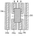
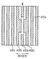
도 9a를 참조하면, 제1 영역 및 제2 영역이 구분되는 기판을 마련한다. 상기 기판 상에 식각 대상막을 형성한다. 상기 식각 대상막 상에 희생 마스크막(도시안함)을 형성한다. 상기 희생 마스크막을 패터닝함으로써, 제1 및 제2 희생 마스크 패턴(244a, 244b)을 각각 형성한다.Referring to FIG. 9A, a substrate having a first region and a second region is provided. A film to be etched is formed on the substrate. A sacrificial mask film (not shown) is formed on the etching target film. The sacrificial mask film is patterned to form the first and second
여기서, 상기 제1 희생 마스크 패턴(244a)은 제1 영역의 기판 상에 형성되며, 끊어진 3개의 제1 라인 패턴 및 끊어진 제1 라인 패턴과 이웃하는 제2 라인 패턴을 형성하기 위한 것이다. 또한, 상기 제2 희생 마스크 패턴(244b)은 제2 영역의 기판 상에 형성되며, 끊어지지 않고 연장되는 제3 라인 패턴들을 형성하기 위한 것이다.Here, the first
상기 제1 희생 마스크 패턴(244a)은 서로 마주하면서 평행한 2개의 끊어진 라인을 포함한다. 본 실시예의 경우, 상기 제1 희생 마스크 패턴(244a) 형성 부위 및 상기 제1 희생 마스크 패턴(244a)들 사이의 갭 부위에 각각 제1 라인 패턴이 형성된다.The first
상기 제2 희생 마스크 패턴(244b)은 라인 및 스페이스가 반복 배치되는 형상을 갖는다.The second
형성하고자 하는 상기 제1 내지 제3 라인 패턴의 선폭이 F라고 할 때, 상기 제1 및 제2 희생 마스크 패턴(244a, 244b) 간의 간격, 제1 희생 마스크 패턴(244a)들 간의 간격 및 상기 제2 희생 마스크 패턴(244b)들 간의 간격도 3F가 된다.The line width of the first to third line patterns to be formed is F, the interval between the first and second
계속하여, 상기 제1 및 제2 희생 마스크 패턴(224a, 224b)의 측벽에 스페이서 패턴(246)을 형성한다. 이 때, 상기 스페이서 패턴들(246) 사이에는 갭(248)들이 생성된다. 이 때, 상기 스페이서 패턴(246)의 선폭과 상기 갭(248)들의 폭은 동일하며, 그 폭은 각각 F일 수 있다.Subsequently, a
본 실시예에서는, 상기 제1 희생 마스크 패턴(244a)이 절단된 라인 형상을 갖는다. 또한, 상기 제1 및 제2 희생 마스크 패턴(244a, 244b) 사이의 갭들 및 상기 제1 희생 마스크 패턴들(244a) 사이의 갭들은 2개의 H자가 붙어있는 형상을 갖는다.In this embodiment, the first
도 9b를 참조하면, 상기 식각 대상막, 스페이서 패턴(246) 및 희생 마스크 패턴들(244a, 244b) 상에 마스크막(도시안함)을 형성한다. 상기 마스크막은 스핀 코팅에 의해 형성될 수 있는 막일 수 있다. 예를들어, 상기 마스크막은 스핀 온 하드 마스크막(SOH) 또는 포토레지스트막일 수 있다.Referring to FIG. 9B, a mask film (not shown) is formed on the etch target film, the
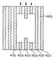
상기 마스크막을 사진공정에 의해 패터닝함으로써 상기 기판의 제1 영역에 마스크 패턴(250)을 형성한다. 상기 마스크 패턴(250)은 상기 제1 희생 마스크 패턴(244a)의 끊어진 라인들의 각 단부를 연결하는 하나의 패드 형상을 갖는다.The mask pattern is patterned by photolithography to form a
상기 제1 희생 마스크 패턴(244a)은 이미 분리가 되어 있으나, 상기 제1 및 제2 희생 마스크 패턴(244a, 244b) 사이의 갭과 상기 제1 희생 마스크 패턴들(244a) 사이의 갭이 서로 분리되지 않기 때문에, 상기 마스크 패턴(250)에 의해 상기 갭을 서로 분리시켜야 한다.Although the first
상기 마스크 패턴(250)은 4F의 폭을 가질 수 있다. 또한, 상기 마스크 패턴(250)이 정 얼라인 되어 있는 경우, 상기 마스크 패턴(250)의 좌, 우측벽은 상기 제1 희생 마스크 패턴(244a)의 각 라인의 중심 부위에 위치한다. 그러나, 상기 마스크 패턴(250)은 정 얼라인되었을 때를 기준으로 좌, 우 1.5F까지 미스 얼라인이 발생하더라도 최종적으로 형성되는 제1 라인 패턴은 상기 마스크 패턴(250)의 형성 영역에서 서로 끊어진 형상을 가질 수 있다. 즉, 상기 마스크 패턴(250)은 좌, 우 1.5F의 미스 얼라인 마진을 갖는다.The
도 9c를 참조하면, 상기 제1 및 제2 희생 마스크 패턴(244a, 244b)을 제거한다. 이 때, 상기 마스크 패턴(250)에 의해 덮혀있는 제1 및 제2 희생 마스크 패턴(244a, 244b)은 제거되지 않는다. 상기 제거 공정은 도 2c를 참조로 설명한 것과 동일하다.Referring to FIG. 9C, the first and second
이 후, 도 2d 내지 도 2f를 참조로 설명한 것과 동일한 공정을 수행함으로써, 도 9d에 도시된 것과 같은 패턴 구조물을 형성한다.Then, by performing the same process as described with reference to Figs. 2D to 2F, a pattern structure as shown in Fig. 9D is formed.
도 9d를 참조하면, 상기 패턴 구조물은 끊겨진 부위를 갖는 라인 형상의 3개의 제1 라인 패턴(254a)이 구비된다. 상기 제1 라인 패턴(254a) 양 측에 각각 하나씩 배치되는 제2 라인 패턴(254b)들 및 상기 제2 라인 패턴(254b) 외곽으로 배치되는 제3 라인 패턴(254c)들을 포함한다. 상기 패턴 구조물 사이에는 식각 대상막 패턴(242a)이 구비된다.Referring to FIG. 9D, the pattern structure is provided with three
상기 제1 라인 패턴(254a)은 상기 제1 희생 마스크 패턴(244a)이 형성되어 있던 부위 및 제1 희생 마스크 패턴(244a) 사이의 갭 부위에 위치하게 된다. 상기 제2 라인 패턴(254b)들은 각각 제1 라인 패턴(254a)과 동일한 방향으로 연장되고 끊겨진 부위가 없는 연장 라인(L3)과, 상기 연장 라인(L3)으로부터 제1 라인 패턴(254a)으로 향하는 방향으로 측방 돌출되는 돌출 패턴(L4)을 포함한다. 상기 마스크 패턴(250)이 정 얼라인되었을 경우에는 서로 마주하는 제2 라인 패턴(254b)이 서로 대칭적인 형상을 갖는다. 그러나, 상기 마스크 패턴(250)이 좌, 우 1.5F 범위 내에서 미스 얼라인되었을 경우에는 서로 마주하는 제2 라인 패턴(254b)의 돌출 패턴(L4)의 너비가 서로 다르게 된다. 상기 제3 라인 패턴(254c)은 라인 및 스페이스가 반복되는 형상을 갖는다. 또한, 상기 마스크 패턴(250)이 미스 얼라인되었을 경우, 상기 제1 라인 패턴(254a)이 끊겨지는 단부의 위치가 각각 달라질 수 있으며, 상기 제1 라인 패턴(254a)의 단부의 너비가 달라질 수도 있다.
The
실시예 5Example 5
도 10a 내지 10d는 본 발명의 실시예 5에 따른 패턴 구조물의 형성 방법을 나타내는 평면도들이다.10A to 10D are plan views showing a method of forming a pattern structure according to a fifth embodiment of the present invention.
본 실시예는 끊어진 라인이 3개인 패턴 구조물을 형성하는 방법에 관한 것이다.This embodiment relates to a method for forming a pattern structure with three broken lines.
도 10a를 참조하면, 제1 영역 및 제2 영역이 구분되는 기판을 마련한다. 상기 기판 상에 식각 대상막을 형성한다. 상기 식각 대상막 상에 희생 마스크막을 형성한다. 상기 희생 마스크막을 패터닝함으로써, 제1 및 제2 희생 마스크 패턴(264a, 264b)을 각각 형성한다.Referring to FIG. 10A, a substrate having a first region and a second region is provided. A film to be etched is formed on the substrate. A sacrificial mask film is formed on the etching target film. The sacrificial mask film is patterned to form the first and second
여기서, 상기 제1 희생 마스크 패턴(264a)은 제1 영역의 기판 상에 형성되며, 끊어진 3개의 제1 라인 패턴 및 끊어진 제1 라인 패턴과 이웃하는 제2 라인 패턴을 형성하기 위한 것이다. 또한, 상기 제2 희생 마스크 패턴(264b)은 제2 영역의 기판 상에 형성되며, 끊어지지 않고 연장되는 제3 라인 패턴들을 형성하기 위한 것이다.Here, the first
상기 제1 희생 마스크 패턴(264a)은 서로 마주하면서 평행한 3개의 연장 라인(L1) 및 상기 연장 라인(L1)들의 일부분을 수평 방향으로 연결하는 연결 라인(L2)을 포함한다. 즉, 상기 제1 희생 마스크 패턴(264a)은 상기 연장 라인(L1) 및 연결 라인(L2)이 2개의 H가 붙어있는 형상을 갖는다. 상기 연결 라인(L2)은 상기 제1 라인 패턴이 끊어지는 위치에 위치한다. 본 실시예의 경우, 상기 서로 마주하는 2개의 연장 라인(L1) 사이의 갭 부위와 상기 3개의 연장 라인 중 가운에에 위치하는 연장 라인이 각각 상기 제1 라인 패턴이 형성되는 영역이 된다.The first
상기 제2 희생 마스크 패턴(264b)은 라인 및 스페이스가 반복 배치되는 형상을 갖는다.The second
형성하고자 하는 상기 제1 내지 제3 라인 패턴의 선폭이 F라고 할 때, 상기 제1 및 상기 제2 희생 마스크 패턴(264a, 264b)들 간의 간격은 3F가 된다. 또한, 상기 제2 희생 마스크 패턴(264b)들 간의 간격도 3F가 된다.When the line width of the first to third line patterns to be formed is F, the gap between the first and second
계속하여, 상기 제1 및 제2 희생 마스크 패턴(264a, 264b)의 측벽에 스페이서 패턴(266)을 형성한다. 이 때, 상기 스페이서 패턴들(266) 사이에는 갭(268a, 268b)들이 생성된다. 이 때, 상기 스페이서 패턴(266)의 선폭과 상기 갭(268a, 268b)들의 폭은 동일하며, 그 폭은 각각 F일 수 있다.Subsequently, a
도 10b를 참조하면, 상기 식각 대상막, 스페이서 패턴(266) 및 희생 마스크 패턴들(264a, 264b) 상에 마스크막(도시안함)을 형성한다. 상기 마스크막은 스핀 코팅에 의해 형성될 수 있는 막일 수 있다. 예를들어, 상기 마스크막은 스핀 온 하드 마스크막(SOH) 또는 포토레지스트막일 수 있다.Referring to FIG. 10B, a mask film (not shown) is formed on the etch target film, the
상기 마스크막을 사진공정에 의해 패터닝함으로써 상기 기판의 제1 영역에 마스크 패턴(270)을 형성한다. 상기 마스크 패턴(270)은 상기 제1 희생 마스크 패턴(264a)의 연장 라인(L1)들 사이의 갭(268a) 부위의 단부를 연결하는 하나의 패드 형상을 갖는다.The mask pattern is patterned by photolithography to form a
상기 제1 희생 마스크 패턴(264a)의 연장 라인(L1) 사이의 갭은 서로 분리되어 있다. 그러나, 상기 제1 희생 마스크 패턴(264a)들은 연결 라인(L2)에 의해 연결되어 있으므로, 상기 마스크 패턴(270)에 의해 상기 연결 라인(L2)을 분리시켜야 한다.The gaps between extension lines L1 of the first
상기 마스크 패턴(270)은 4F의 폭을 가질 수 있다. 또한, 상기 마스크 패턴(270)이 정 얼라인되어 있는 경우, 상기 마스크 패턴(270)은 상기 제1 희생 마스크 패턴(264a)의 중심 부위에 위치한다. 그러나, 상기 마스크 패턴(270)은 정 얼라인되었을 때를 기준으로 좌, 우 1.5F까지 미스 얼라인이 발생하더라도 최종적으로 형성되는 3개의 제1 라인 패턴(274a)은 상기 마스크 패턴(270)의 형성 영역에서 서로 끊어진 형상을 가질 수 있다. 즉, 상기 마스크 패턴은 좌, 우 1.5F의 미스 얼라인 마진을 갖는다.The
도 10c를 참조하면, 상기 제1 및 제2 희생 마스크 패턴(264a, 264b)을 제거한다. 이 때, 상기 마스크 패턴(270)에 의해 덮혀있는 제1 및 제3 희생 마스크 패턴(264a, 264b)은 제거되지 않는다. 상기 제거 공정은 도 2c를 참조로 설명한 것과 동일하다.Referring to FIG. 10C, the first and second
이 후, 도 2d 내지 도 2f를 참조로 설명한 것과 동일한 공정을 수행함으로써, 도 10d에 도시된 것과 같은 패턴 구조물을 형성한다.Thereafter, the same process as described with reference to Figs. 2D to 2F is performed to form a pattern structure as shown in Fig. 10D.
도 10d를 참조하면, 상기 패턴 구조물은 끊겨진 부위를 갖는 라인 형상의 3개의 제1 라인 패턴(274a)이 구비된다. 상기 제1 라인 패턴(274a) 양 측에 각각 하나씩 배치되는 제2 라인 패턴(274b)들 및 상기 제2 라인 패턴(274b) 외곽으로 배치되는 제3 라인 패턴(274c)들을 포함한다. 상기 패턴 구조물은 도 9d에 도시된 패턴 구조물과 동일한 형상을 갖는다. 다만, 본 실시예의 경우, 상기 제1 희생 마스크 패턴(264a)의 연장 라인(L1)들 사이의 2개의 갭 부위(268a) 및 제1 희생 마스크 패턴(264a) 의 중심부에 위치하는 연장 라인 영역에 제1 라인 패턴이 생성되는 것에서만 도 9d의 패턴 구조물과 다르다.
Referring to FIG. 10D, the pattern structure is provided with three
실시예 6Example 6
도 11a 내지 도 11e는 본 발명의 실시예 6에 따른 패턴 구조물의 형성 방법을 나타내는 평면도들이다. 도 12a 내지 도 12f는 도 11e에 도시된 패턴 구조물의 형성 방법을 나타내는 단면도들이다. 도 12a 내지 도 12f는 도 11b의 II-II'부위를 절단하였을 때 보여지는 단면도들이다.11A to 11E are plan views showing a method of forming a pattern structure according to a sixth embodiment of the present invention. 12A to 12F are cross-sectional views illustrating a method of forming the pattern structure shown in FIG. 11E. Figs. 12A to 12F are cross-sectional views taken along the line II-II 'of Fig. 11B.
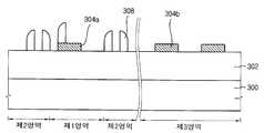
본 실시예는 2개의 끊어진 제1 라인 패턴을 포함하는 패턴 구조물을 형성하는 방법에 관한 것이다.This embodiment relates to a method of forming a pattern structure including two broken first line patterns.
도 11a 및 도 12a를 참조하면, 제1 영역 및 제2 영역이 구분되는 기판(300)을 마련한다. 상기 기판(300)의 제1 영역은 끊어진 제1 라인 패턴들 및 끊어진 제1 라인 패턴들 양 측의 이웃하는 제2 라인 패턴들이 형성되기 위한 영역이다. 또한, 상기 기판(300)의 제2 영역은 제1 영역 이외의 나머지 영역으로 라인 및 스페이스(line and space)가 반복 형성되는 제3 라인 패턴들이 형성되는 영역이다.Referring to FIGS. 11A and 12A, a
상기 기판(300) 상에 식각 대상막(302)을 형성한다. 상기 식각 대상막(302)은 실리콘 산화물 또는 실리콘 질화물과 같은 절연막일 수 있다. 이와는 다른 예로, 상기 식각 대상막(302)이 별도로 형성되지 않고, 기판(300) 자체가 식각 대상물이 될 수도 있다.A
상기 식각 대상막(302) 상에 하드 마스크막을 형성한다. 상기 하드 마스크막은 상기 식각 대상막과 식각 선택비가 높은 물질로 형성한다. 일 예로, 상기 하드 마스크막은 실리콘 질화물, 실리콘 산질화막 또는 폴리실리콘으로 형성될 수 있다. 본 실시예에서, 상기 하드 마스크막은 실리콘 질화물로 형성한다.A hard mask film is formed on the
상기 하드 마스크막을 패터닝하여 예비 하드 마스크 패턴(304)을 형성한다. 상기 예비 하드 마스크 패턴(304)은 끊어진 라인을 형성하기 위한 부위에 위치하며, 패드 형상을 갖는다. 형성하고자 하는 제1 내지 제3 라인 패턴의 선폭이 F인 경우, 상기 예비 하드 마스크 패턴(304)은 4F의 폭을 갖는다.The hard mask film is patterned to form a preliminary
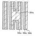
도 11b 및 도 12b를 참조하면, 상기 예비 하드 마스크 패턴(304)이 형성된 식각 대상막(302) 상에 희생 마스크막(도시안함)을 형성한다. 상기 희생 마스크막은 스핀 온 방식으로 형성되는 하드 마스크(SOH) 또는 포토레지스트로 형성될 수 있다. 상기 희생 마스크막을 패터닝함으로써, 제1 및 제2 희생 마스크 패턴(306a, 306b)을 각각 형성한다.Referring to FIGS. 11B and 12B, a sacrificial mask film (not shown) is formed on the
여기서, 상기 제1 희생 마스크 패턴(306a)은 제1 영역의 기판(300) 상에 형성되며, 끊어진 제1 라인 패턴들 및 끊어진 제1 라인 패턴들과 이웃하는 제2 라인 패턴들을 형성하기 위한 것이다. 또한, 상기 제2 희생 마스크 패턴(306b)은 제2 영역의 기판(300)상에 형성되며, 끊어지지 않고 연장되는 제3 라인 패턴들을 형성하기 위한 것이다.Here, the first
상기 제1 희생 마스크 패턴(306a)은 서로 마주하면서 평행한 2개의 연장 라인(L1) 및 상기 연장 라인(L1)의 일부분을 수평 방향으로 연결하는 연결 라인(L2)을 포함한다. 상기 제1 희생 마스크 패턴(306a)은 상기 연장 라인(L1) 및 연결 라인(L2)이 H 형상을 갖는다. 또한, 상기 연장 라인(L1)들은 1F의 선폭을 갖고, 상기 연장 라인(L1)들 간의 간격은 3F이다.The first
이 때, 상기 제1 희생 마스크 패턴(306a)이 정 얼라인된 위치에 놓여지기 위해서는, 상기 제1 희생 마스크 패턴(306a)에서 좌측의 연장 라인(L1)이 상기 예비 하드 마스크 패턴(304)의 중심 부위에 놓여진다. 그러나, 상기 제1 희생 마스크 패턴(306a)은 좌, 우로 1.5F씩의 미스 얼라인 마진을 가지므로, 상기 미스 얼라인 마진 내의 범위에서 좌우로 미스 얼라인 되더라도 불량이 발생되지 않는다.At this time, in order to place the first
상기 제2 희생 마스크 패턴(306b)은 라인 및 스페이스가 반복되는 형상을 갖는다. 상기 제2 희생 마스크 패턴(306b)은 1F의 선폭을 갖고, 상기 제2 희생 마스크 패턴(306b) 간의 간격은 3F이다.The second
도 11c를 참조하면, 상기 제1 및 제2 희생 마스크 패턴(306a, 306b)과 상기 예비 하드 마스크 패턴(304) 표면을 따라 스페이서막(도시안함)을 형성한다. 상기 스페이서막은 상기 제1 및 제2 희생 마스크 패턴(306a, 306b)과 다른 식각 특성을 갖는 물질로 이루어질 수 있다. 예를들어, 상기 스페이서막은 실리콘 산화물로 형성될 수 있다. 상기 스페이서막은 균일한 두께를 갖도록 형성하기 위하여 ALD (atomic layer deposition) 공정을 이용할 수 있다.Referring to FIG. 11C, a spacer film (not shown) is formed along the surfaces of the first and second
상기 스페이서막을 에치백하여 상기 제1 및 제2 희생 마스크 패턴(306a, 306b)의 측벽에는 각각 스페이서 패턴(308)을 형성한다. 계속하여, 상기 스페이서 패턴(308)의 양 측으로 노출되는 상기 예비 하드 마스크 패턴(304)을 식각한다. 상기 식각 공정을 수행하면, 상기 제1 및 제2 희생 마스크 패턴(306a, 306b)과 상기 스페이서 패턴(308) 아래에 하드 마스크 패턴(304a)이 형성된다.The spacer film is etched back to form a
상기 예비 하드 마스크 패턴(304)이 정 위치에 위치하지 않더라도, 상기 스페이서 패턴(308)을 형성한 후에 하부의 예비 하드 마스크 패턴(304)을 형성하면 상기 스페이서 패턴(308)에 의해 자기 정렬된 하드 마스크 패턴(304a)을 형성할 수 있다. 그러므로, 상기 예비 하드 마스크 패턴(304)과 상기 제1 희생 마스크 패턴(306a) 간의 미스 얼라인 마진을 증가시킬 수 있다.Even if the spare
도 11d 및 도 12d를 참조하면, 상기 제1 및 제2 희생 마스크 패턴(306a, 306b)을 제거한다. 이 때, 상기 하드 마스크 패턴(304a)은 제거되지 않고 남아있게 된다.Referring to FIGS. 11D and 12D, the first and second
상기 공정에 의해 남아있는 스페이서 패턴(308)들과 하드 마스크 패턴(304a)은 상기 식각 대상막을 식각하기 위한 실질적인 식각 마스크의 역할을 한다. 본 실시예에서는 다마신 방식으로 패턴 구조물을 형성하므로, 상기 식각 대상막(302)이 노출되어 있는 부위에 패턴 구조물이 형성된다.The remaining
도 11e 및 도 12e를 참조하면, 상기 스페이서 패턴들(308)과 하드 마스크 패턴(304a)을 식각 마스크로 사용하여 상기 식각 대상막(302)을 식각함으로써, 개구부(310)들을 포함하는 식각 대상막 패턴(302a)을 형성한다. 상기 식각 대상막 패턴(302a)을 형성한 다음, 상기 스페이서 패턴들(308) 및 하드 마스크 패턴(304a)을 제거한다.Referring to FIGS. 11E and 12E, the
도 11f 및 도 12f를 참조하면, 상기 개구부(310)들 내부를 채우는 매립막(도시안함)을 형성한다. 이 후, 상기 식각 대상막 패턴(302a)의 상부면이 노출되도록 상기 매립막을 연마함으로써 패턴 구조물을 형성한다.Referring to FIGS. 11F and 12F, a buried layer (not shown) filling the
상기 공정을 수행하여 형성되는 상기 패턴 구조물은 끊겨진 부위를 갖는 라인 형상의 제1 라인 패턴(312a)들과, 상기 제1 라인 패턴(312a) 양 측에 각각 하나씩 배치되는 제2 라인 패턴(312b)들 및 상기 제2 라인 패턴(312b) 외곽으로 배치되는 제3 라인 패턴(312c)들을 포함한다. 상기 제1 라인 패턴(312a)은 2개가 구비된다.The pattern structure formed by performing the above process includes a
상기 제2 라인 패턴(312b) 중 하나는 상기 제1 라인 패턴(312a)과 동일한 방향으로 연장되고 끊겨진 부위가 없는 연장 라인(L3)과, 상기 연장 라인(L3)으로부터 제1 라인 패턴(312a)으로 향하는 방향으로 측방 돌출되는 돌출 패턴(L4)을 포함한다. 또한, 나머지 하나의 제2 라인 패턴(312b)은 돌출 패턴없이 연장되는 라인 형상을 갖는다. 그러나, 상기 제2 라인 패턴(312b)은 상기 하드 마스크 패턴(304a)의 미스 얼라인에 따라 그 형상이 달라질 수 있다.One of the
상기 제3 라인 패턴(312c)은 라인 및 스페이스가 반복되는 형상을 갖는다.
The
도 13a 내지 13d는 본 발명의 일 실시예에 따른 패턴 구조물의 형성 방법을 나타내는 평면도들이다.13A to 13D are plan views illustrating a method of forming a pattern structure according to an embodiment of the present invention.
이하에서 설명하는 패턴 구조물의 형성 방법은 상기 하드 마스크 패턴의 위치가 제1 희생 마스크 패턴의 중심을 기준으로 도 11a에 도시된 것과 좌, 우 대칭하게 배치되는 것을 제외하고는 도 11a 내지 도 11f를 참조로 설명한 것과 동일하다. 또한, 상기 방법을 통해 형성되는 패턴 구조물은 도 12f에 도시된 것과 좌, 우 대칭인 형상을 갖는다.11A to 11F, except that the position of the hard mask pattern is symmetrically arranged left and right as shown in Fig. 11A with respect to the center of the first sacrificial mask pattern, Which is the same as described with reference. Further, the pattern structure formed through the above method has a shape symmetrical to the left and right as shown in Fig. 12F.
도 13a를 참조하면, 기판 상에 식각 대상막을 형성하고, 상기 식각 대상막 상에 예비 하드 마스크 패턴(304')을 형성한다. 상기 예비 하드 마스크 패턴(304')은 상기 식각 대상막과 식각 선택비가 높은 물질로 형성한다. 일 예로, 상기 예비 하드 마스크 패턴(304')은 실리콘 질화물, 실리콘 산질화막 또는 폴리실리콘으로 형성될 수 있다.Referring to FIG. 13A, a film to be etched is formed on a substrate, and a preliminary hard mask pattern 304 'is formed on the film to be etched. The preliminary hard mask pattern 304 'is formed of a material having a high etch selectivity with respect to the etch target film. As an example, the preliminary hard mask pattern 304 'may be formed of silicon nitride, silicon oxynitride, or polysilicon.
상기 예비 하드 마스크 패턴(304')은 끊어진 라인을 형성하기 위한 부위에 위치하며, 패드 형상을 갖는다. 형성하고자 하는 제1 내지 제3 라인 패턴의 선폭이 F인 경우, 상기 예비 하드 마스크 패턴(304')은 4F의 폭을 갖는다.The preliminary hard mask pattern 304 'is located at a portion for forming a broken line and has a pad shape. When the line width of the first to third line patterns to be formed is F, the preliminary hard mask pattern 304 'has a width of 4F.
상기 예비 하드 마스크 패턴(304')이 형성된 식각 대상막 상에 제1 및 제2 희생 마스크 패턴(306a, 306b)을 형성한다. 상기 제1 및 제2 희생 마스크 패턴(306a, 306b)은 도 11b에 도시된 것과 동일한 형상을 갖는다. 그러나, 도 11b와는 달리, 상기 제1 희생 마스크 패턴(306a)이 정 얼라인된 위치에 놓여지기 위해서는, 상기 제1 희생 마스크 패턴(306a)에서 우측의 연장 라인이 예비 하드 마스크 패턴(304')의 중심 부위에 놓여진다. 그러나, 상기 제1 희생 마스크 패턴(306a)은 좌, 우로 1.5F씩의 미스 얼라인 마진을 가지므로, 상기 미스 얼라인 마진 내의 범위에서 좌우로 미스 얼라인되더라도 불량이 발생되지 않는다.First and second
도 13b를 참조하면, 상기 제1 및 제2 희생 마스크 패턴(306a, 306b)의 양 측벽에 스페이서 패턴(308)을 형성한다. 계속하여, 상기 스페이서 패턴(308)의 양 측으로 노출되는 상기 예비 하드 마스크 패턴(304')을 식각한다. 상기 식각 공정을 수행하면, 상기 제1 및 제2 희생 마스크 패턴(306a, 306b)과 상기 스페이서 패턴(308) 아래에 하드 마스크 패턴(304a')이 형성된다. 상기 공정은 도 11c를 참조로 설명한 것과 동일하다.Referring to FIG. 13B, a
도 13c를 참조하면, 상기 제1 및 제2 희생 마스크 패턴(306a, 306b)을 제거한다. 이 때, 상기 하드 마스크 패턴(304a')은 제거되지 않고 남아있게 된다.Referring to FIG. 13C, the first and second
이 후, 도 11d 내지 도 11f를 참조로 설명한 것과 동일한 공정을 수행함으로써, 13d에 도시된 것과 같은 패턴 구조물을 형성한다.Then, by performing the same process as described with reference to Figs. 11D to 11F, a pattern structure as shown in Fig. 13D is formed.
도 13d를 참조하면, 상기 패턴 구조물은 도 11f에 도시된 패턴 구조물과 좌, 우 대칭된 형상을 갖는다.
Referring to FIG. 13D, the pattern structure has the pattern structure shown in FIG. 11F and the left and right symmetrical shapes.
실시예 7Example 7
도 14a 내지 14d는 본 발명의 실시예 7에 따른 패턴 구조물의 형성 방법을 나타내는 평면도들이다.14A to 14D are plan views showing a method of forming a pattern structure according to a seventh embodiment of the present invention.
본 실시예는 끊어진 라인이 1개인 패턴 구조물을 형성하는 방법에 관한 것이다.This embodiment relates to a method for forming a pattern structure with one broken line.
도 14a를 참조하면, 제1 영역 및 제2 영역이 구분되는 기판을 마련한다. 상기 기판 상에 식각 대상막을 형성한다. 상기 식각 대상막 상에 예비 하드 마스크 패턴(404)을 형성한다. 상기 예비 하드 마스크 패턴(404)은 끊어진 라인을 형성하기 위한 부위에 위치하며, 패드 형상을 갖는다. 형성하고자 하는 제1 내지 제3 라인 패턴의 선폭이 F인 경우, 상기 예비 하드 마스크 패턴(404)은 4F의 폭을 갖는다.Referring to FIG. 14A, a substrate on which a first region and a second region are separated is provided. A film to be etched is formed on the substrate. A preliminary
상기 예비 하드 마스크 패턴(404) 상에 끊어진 제1 라인 패턴 및 상기 제1 라인 패턴과 이웃하는 제2 라인 패턴을 형성하기 위한 제1 희생 마스크 패턴(406a)과, 끊어지지 않고 라인 및 스페이스가 반복되는 제3 라인 패턴을 형성하기 위한 제2 희생 마스크 패턴(406b)을 형성한다. 본 실시예의 경우, 상기 제1 및 제2 희생 마스크 패턴(406a, 406b)은 끊어지는 부분없이 연장되는 라인 형상을 갖는다. 상기 제1 및 제2 희생 마스크 패턴(406a, 406b)은 1F의 선폭을 갖고 3F의 간격으로 서로 이격된다.A first
정 얼라인되었을 때, 상기 제1 희생 마스크 패턴(406a)은 상기 예비 하드 마스크 패턴(404)의 중심 부위에 위치한다. 그러나, 상기 예비 하드 마스크 패턴(404)은 좌, 우로 1.5F씩의 미스 얼라인 마진을 가지므로, 상기 미스 얼라인 마진 내의 범위에서 좌우로 미스 얼라인되더라도 불량이 발생되지 않는다.When the mask is aligned, the first
도 14b를 참조하면, 상기 제1 및 제2 희생 마스크 패턴(406a, 406b)의 측벽에 스페이서 패턴(408)을 형성한다. 계속하여, 상기 스페이서 패턴(408)의 양 측으로 노출되는 상기 예비 하드 마스크 패턴(404)을 식각한다. 상기 식각 공정에 의해, 상기 스페이서 패턴(408) 아래에 하드 마스크 패턴(404a)이 형성된다. 상기 공정은 도 12c에서 설명한 것과 동일하다.Referring to FIG. 14B, a
상기 예비 하드 마스크 패턴(404)이 정 위치에 위치하지 않더라도 상기 스페이서 패턴(408)을 형성한 후에 하부의 예비 하드 마스크 패턴이 일부 식각되므로, 상기 스페이서 패턴(408)에 의해 자기 정렬된 하드 마스크 패턴(404a)을 형성할 수 있다. 그러므로, 상기 예비 하드 마스크 패턴(404)과 상기 제1 및 제2 희생 마스크 패턴(406a, 406b) 간의 미스 얼라인 마진을 증가시킬 수 있다.Even if the preliminary
도 14c를 참조하면, 상기 제1 및 제2 희생 마스크 패턴(406a, 406b)을 제거한다. 이 때, 상기 하드 마스크 패턴(404a)은 제거되지 않고 남아있게 된다. 상기 공정은 도 12d를 참조로 설명한 것과 동일하다.Referring to FIG. 14C, the first and second
계속하여 12e 및 12f를 참조로 설명한 공정들을 수행하여 도 14d의 패턴 구조물을 형성한다.Subsequently, the processes described with reference to 12e and 12f are performed to form the pattern structure of FIG. 14d.
도 14d를 참조하면, 상기 제1 희생 마스크 패턴(406a)이 제거된 부위에 끊겨진 제1 라인 패턴(412a)이 형성된다. 상기 제1 라인 패턴(412a)들 양 측에는 돌출된 부위없이 연장되는 제2 라인 패턴(412b)이 형성된다. 또한, 상기 제2 라인 패턴(412b) 양 측으로 라인 및 스페이스가 반복 배치되는 제3 라인 패턴(412c)이 구비된다. 본 실시예의 경우, 제2 및 제3 라인 패턴(412b, 412c)이 동일한 형상을 갖는다.
Referring to FIG. 14D, a broken first line pattern 412a is formed at a portion where the first
실시예 8Example 8
도 15a 내지 15d는 본 발명의 실시예 8에 따른 패턴 구조물의 형성 방법을 나타내는 평면도들이다.15A to 15D are plan views showing a method of forming a pattern structure according to an eighth embodiment of the present invention.
본 실시예는 끊어진 라인이 1개인 패턴 구조물을 형성하는 방법에 관한 것이다.This embodiment relates to a method for forming a pattern structure with one broken line.
도 15a를 참조하면, 제1 영역 및 제2 영역이 구분되는 기판을 마련한다. 상기 기판 상에 식각 대상막을 형성한다. 상기 식각 대상막 상에 예비 하드 마스크 패턴(424)을 형성한다. 상기 예비 하드 마스크 패턴(424)은 끊어진 라인을 형성하기 위한 부위에 위치하며, 패드 형상을 갖는다. 형성하고자 하는 제1 내지 제3 라인 패턴의 선폭이 F인 경우, 상기 예비 하드 마스크 패턴(424)은 F의 폭을 갖는다.Referring to FIG. 15A, a substrate having a first region and a second region is provided. A film to be etched is formed on the substrate. A preliminary
상기 예비 하드 마스크 패턴(424) 상에 끊어진 제1 라인 패턴 및 상기 제1 라인 패턴과 이웃하는 제2 라인 패턴을 형성하기 위한 제1 희생 마스크 패턴(426a)을 형성한다. 또한, 끊어지지 않고 라인 및 스페이스가 반복되는 제3 라인 패턴을 형성하기 위한 제2 희생 마스크 패턴(426b)을 형성한다.A first
상기 제1 희생 마스크 패턴(426a)은 도 11b에 도시된 제1 희생 마스크 패턴과 동일한 형상을 갖는다. 즉, 상기 제1 희생 마스크 패턴(426a)은 서로 마주하는 연장 라인(L1) 및 상기 연장 라인(L1)을 수평 연결하는 연결 라인(L2)이 구비되어 전체적으로 H자 형상을 갖는다.The first
정얼라인되었을 때, 상기 예비 하드 마스크 패턴(424)은 상기 제1 희생 마스크 패턴(426a)의 연결 라인(L2)의 중심 부위의 아래에 위치하고 상기 연결 라인(L2)의 저면을 가로지르도록 형성하여야 한다. 그러나, 상기 제1 희생 마스크 패턴(426a)은 좌, 우로 1.5F 씩의 미스 얼라인 마진을 가지므로, 상기 미스 얼라인 마진 내의 범위에서 좌우로 미스 얼라인되더라도 불량이 발생되지 않는다.The preliminary
상기 제2 희생 마스크 패턴(426b)은 라인 및 스페이스가 반복되는 형상을 가진다. 상기 제2 희생 마스크 패턴(426b)의 선폭은 F이고, 상기 제2 희생 마스크 패턴(426b) 간의 간격은 3F이다.The second
도 15b를 참조하면, 상기 제1 및 제2 희생 마스크 패턴(426a, 426b)의 측벽에 스페이서 패턴(428)을 형성한다. 계속하여, 상기 스페이서 패턴(428)의 양 측으로 노출되는 상기 예비 하드 마스크 패턴(424)을 식각한다. 상기 식각 공정에 의해, 상기 스페이서 패턴(428) 및 제1 희생 마스크 패턴(426a) 아래에 하드 마스크 패턴(424a)이 형성된다. 상기 공정은 도 12c에서 설명한 것과 동일하다.Referring to FIG. 15B, a
도 15c를 참조하면, 상기 제1 및 제2 희생 마스크 패턴(426a, 426b)을 제거한다. 이 때, 상기 하드 마스크 패턴(424a)은 제거되지 않고 남아있게 된다. 상기 공정은 도 12d를 참조로 설명한 것과 동일하다.Referring to FIG. 15C, the first and second
계속하여 12e 및 12f를 참조로 설명한 공정들을 수행하여 도 15d에 도시된 것과 같이 제1 내지 제3 라인 패턴(432a, 432b, 432c)을 포함하는 패턴 구조물을 형성한다. 또한, 상기 패턴 구조물 사이에는 식각 대상막 패턴(422a)이 구비된다.Subsequently, the processes described with reference to 12e and 12f are performed to form a pattern structure including the first to third line patterns 432a, 432b, and 432c as shown in FIG. 15D. In addition, a
도 15d를 참조하면, 상기 패턴 구조물은 도 14d의 패턴 구조물과 동일한 형상을 갖는다. 다만, 도 15d의 패턴 구조물에서 제1 라인 패턴(432a)은 상기 제1 희생 마스크 패턴(426a)의 연장 라인 사이의 갭 부위에 형성되는 점이 도 14d의 패턴 구조물과 다르다.
Referring to FIG. 15D, the pattern structure has the same shape as the pattern structure of FIG. 14D. However, the pattern structure of FIG. 15D differs from the pattern structure of FIG. 14D in that the first line pattern 432a is formed at the gap between the extension lines of the first
실시예 9Example 9
도 16a 내지 16d는 본 발명의 실시예 9에 따른 패턴 구조물의 형성 방법을 나타내는 평면도들이다.16A to 16D are plan views showing a method of forming a pattern structure according to a ninth embodiment of the present invention.
본 실시예는 끊어진 라인이 3개인 패턴 구조물을 형성하는 방법에 관한 것이다.This embodiment relates to a method for forming a pattern structure with three broken lines.
도 16a를 참조하면, 제1 영역 및 제2 영역이 구분되는 기판을 마련한다. 상기 기판 상에 식각 대상막을 형성한다. 상기 식각 대상막 상에 예비 하드 마스크 패턴(444)을 형성한다. 상기 예비 하드 마스크 패턴(444)은 끊어진 라인을 형성하기 위한 부위에 위치하며, 패드 형상을 갖는다. 형성하고자 하는 제1 내지 제3 라인 패턴의 선폭이 F인 경우, 상기 예비 하드 마스크 패턴(444)은 8F의 폭을 갖는다.16A, a substrate on which a first region and a second region are separated is provided. A film to be etched is formed on the substrate. A preliminary
상기 예비 하드 마스크 패턴(444) 상에 끊어진 제1 라인 패턴 및 상기 제1 라인 패턴과 이웃하는 제2 라인 패턴을 형성하기 위한 제1 희생 마스크 패턴(446a)과, 끊어지지 않고 라인 및 스페이스가 반복되는 제3 라인 패턴을 형성하기 위한 제2 희생 마스크 패턴(446b)을 형성한다.A first
상기 제1 희생 마스크 패턴(446a)은 도 11b에 도시된 제1 희생 마스크 패턴과 동일한 형상을 갖는다. 즉, 상기 제1 희생 마스크 패턴(446a)은 서로 마주하는 연장 라인(L1) 및 상기 연장 라인(L1)을 수평 연결하는 연결 라인(L2)이 구비되어 전체적으로 H자 형상을 갖는다. 이 때, 상기 연장 라인(L1)들 간의 간격은 3F가 되도록 한다.The first
정얼라인되었을 때, 상기 예비 하드 마스크 패턴(444)은 상기 제1 희생 마스크 패턴(446a)의 연결 라인(L2)의 중심 부위의 아래에 위치하여야 한다. 그러나, 상기 제1 희생 마스크 패턴(446a)은 좌, 우로 1.5F 씩의 미스 얼라인 마진을 가지므로, 상기 미스 얼라인 마진 내의 범위에서 좌우로 미스 얼라인되더라도 불량이 발생되지 않는다.When aligned, the preliminary
상기 제2 희생 마스크 패턴(446b)은 라인 및 스페이스가 반복되는 형상을 가진다. 상기 제2 희생 마스크 패턴(446b)의 선폭은 F이고, 상기 제2 희생 마스크 패턴(446b) 간의 간격은 3F이다.The second
도 16b를 참조하면, 상기 제1 및 제2 희생 마스크 패턴(446a, 446b)의 측벽에 스페이서 패턴(448)을 형성한다. 계속하여, 상기 스페이서 패턴(448)의 양 측으로 노출되는 상기 예비 하드 마스크 패턴(444)을 식각한다. 상기 식각 공정에 의해, 상기 스페이서 패턴(448) 및 제1 희생 마스크 패턴(446a) 아래에 하드 마스크 패턴(444a)이 형성된다. 상기 공정은 도 12c에서 설명한 것과 동일하다.Referring to FIG. 16B, a
도 16c를 참조하면, 상기 제1 및 제2 희생 마스크 패턴(446a, 446b)을 제거한다. 이 때, 상기 하드 마스크 패턴(444a)은 제거되지 않고 남아있게 된다. 상기 공정은 도 12d를 참조로 설명한 것과 동일하다.Referring to FIG. 16C, the first and second
계속하여 12e 및 12f를 참조로 설명한 공정들을 수행하여 도 16d의 패턴 구조물(452a~452c)을 형성한다.Subsequently, the processes described with reference to 12e and 12f are performed to form the
도 16d를 참조하면, 상기 패턴 구조물은 상기 제1 희생 마스크 패턴(446a)이 제거된 부위 및 상기 제1 희생 마스크 패턴(446a)들의 연장 라인(L1) 사이의 갭 부위에 끊겨진 제1 라인 패턴(452a)이 형성된다. 3개의 상기 제1 라인 패턴들(452a)은 각 단부의 위치가 서로 다를 수도 있고, 동일할 수도 있다.Referring to FIG. 16D, the pattern structure may include a first line pattern in which the first
상기 제1 라인 패턴들(452a) 양 측에는 돌출된 부위없이 연장되는 제2 라인 패턴(452b)이 형성된다. 또한, 상기 제2 라인 패턴(452b) 양 측으로 라인 및 스페이스가 반복 배치되는 제3 라인 패턴(452c)이 구비된다. 본 실시예의 경우, 제2 및 제3 라인 패턴(452b, 452c)이 동일한 형상을 갖는다. 상기 패턴 구조물들 사이에는 식각 대상막 패턴(442a)이 구비된다.
On both sides of the
실시예 10Example 10
도 17a 내지 17d는 본 발명의 실시예 10에 따른 패턴 구조물의 형성 방법을 나타내는 평면도들이다.17A to 17D are plan views showing a method of forming a pattern structure according to a tenth embodiment of the present invention.
본 실시예는 끊어진 라인이 3개인 패턴 구조물을 형성하는 방법에 관한 것이다.This embodiment relates to a method for forming a pattern structure with three broken lines.
도 17a를 참조하면, 제1 영역 및 제2 영역이 구분되는 기판을 마련한다. 상기 기판 상에 식각 대상막을 형성한다. 상기 식각 대상막 상에 예비 하드 마스크 패턴(464)을 형성한다. 상기 예비 하드 마스크 패턴(464)은 끊어진 라인을 형성하기 위한 부위에 위치하며, 패드 형상을 갖는다. 형성하고자 하는 제1 내지 제3 라인 패턴의 선폭이 F인 경우, 상기 예비 하드 마스크 패턴(464)은 4F의 폭을 갖는다.Referring to FIG. 17A, a substrate on which a first region and a second region are separated is provided. A film to be etched is formed on the substrate. A preliminary
상기 예비 하드 마스크 패턴(464)이 형성된 식각 대상막 상에 제1 및 제2 희생 마스크 패턴(466a, 466b)을 형성한다.First and second
상기 제1 희생 마스크 패턴(466a)은 도 10b에 도시된 제1 희생 마스크 패턴과 동일한 형상을 갖는다. 즉, 상기 제1 희생 마스크 패턴(466a)은 서로 평행한 3개의 연장 라인(L1) 및 상기 연장 라인(L1)들을 수평 연결하는 연결 라인(L2)이 구비되어 전체적으로 2개의 붙어있는 H자 형상을 갖는다. 이 때, 상기 연장 패턴(L1)들 간의 간격은 3F가 되도록 한다.The first
정얼라인되었을 때, 상기 예비 하드 마스크 패턴(464)은 상기 제1 희생 마스크 패턴(466a)의 연결 라인(L2)의 중심 부위의 아래에 위치하여야 한다. 그러나, 상기 제1 희생 마스크 패턴(466a)은 좌, 우로 1.5F 씩의 미스 얼라인 마진을 가지므로, 상기 미스 얼라인 마진 내의 범위에서 좌우로 미스 얼라인되더라도 불량이 발생되지 않는다.When aligned, the preliminary
상기 제2 희생 마스크 패턴(466b)은 라인 및 스페이스가 반복되는 형상을 가진다. 상기 제2 희생 마스크 패턴(466b)의 선폭은 F이고, 상기 제2 희생 마스크 패턴(466b) 간의 간격은 3F이다.The second
도 17b를 참조하면, 상기 제1 및 제2 희생 마스크 패턴(466a, 466b)의 측벽에 스페이서 패턴(468)을 형성한다. 계속하여, 상기 스페이서 패턴(468)의 양 측으로 노출되는 상기 예비 하드 마스크 패턴(464)을 식각한다. 상기 식각 공정에 의해, 상기 스페이서 패턴(468) 및 제1 희생 마스크 패턴(466a) 아래에 하드 마스크 패턴(464a)이 형성된다. 상기 공정은 도 12c에서 설명한 것과 동일하다.Referring to FIG. 17B, a
도 17c를 참조하면, 상기 제1 및 제2 희생 마스크 패턴(466a, 466b)을 제거한다. 이 때, 상기 하드 마스크 패턴(464a)은 제거되지 않고 남아있게 된다. 상기 공정은 도 12d를 참조로 설명한 것과 동일하다.Referring to FIG. 17C, the first and second
계속하여 12e 및 12f를 참조로 설명한 공정들을 수행하여 도 17d의 패턴 구조물을 형성한다. 상기 패턴 구조물 사이에는 식각 대상막 패턴(462a)이 구비된다.Subsequently, the processes described with reference to 12e and 12f are performed to form the pattern structure of Figure 17d. A film pattern to be etched 462a is provided between the pattern structures.
도 17d를 참조하면, 상기 패턴 구조물은 끊겨진 3개의 제1 라인 패턴(472a)이 형성된다. 상기 제1 라인 패턴(472a)은 상기 제1 희생 마스크 패턴(466a)의 연장 라인(L1)들 사이의 갭 부위 및 상기 제1 희생 마스크 패턴(466a)들 중에서 가운데에 위치하는 연장 라인(L1) 부위에 위치한다. 3개의 상기 제1 라인 패턴들(472a)은 각 단부의 위치가 서로 다를 수도 있고, 동일할 수도 있다.Referring to FIG. 17D, the pattern structure is formed with three broken
상기 제2 라인 패턴들(472b)은 각각 상기 제1 라인 패턴(472a)의 연장 방향으로 연장되는 연장 라인(L3)과 상기 연장 라인(L3)으로부터 상기 제1 라인 패턴(472a) 방향으로 각각 돌출되는 돌출 패턴(L4)을 포함한다.The
상기 하드 마스크 패턴(464a)이 정 얼라인되었을 경우에는 서로 마주하는 제2 라인 패턴(472b)이 좌우 대칭된 형상을 갖는다. 그러나, 상기 하드 마스크 패턴(464a)이 좌, 우 1.5F 범위 내에서 미스 얼라인되었을 경우에는 서로 마주하는 제2 라인 패턴(472b)의 돌출 패턴의 너비가 서로 다르게 된다.When the
상기 제3 라인 패턴(472c)은 라인 및 스페이스가 반복되는 형상을 갖는다.The
상기에서 설명한 것과 같이, 라인 및 스페이스가 반복되는 라인 패턴들 중간 또는 끝부분에 끊어지는 라인들을 포함하는 라인 패턴 구조물들을 형성할 수 있다.
As described above, line pattern structures can be formed that include lines that break at the middle or end of line patterns where lines and spaces are repeated.
이하에서는, 상기 라인 및 스페이스가 반복되는 라인 패턴들 중간 또는 끝부분에 끊어지는 라인들을 포함하는 라인 패턴 구조물들과, 상기 라인 패턴들보다 넓은 선폭을 갖는 페리용 라인 또는 패드들을 함께 형성하는 방법에 대해 설명하고자 한다. 상기 라인 패턴 구조물들을 형성하는 공정은 각 실시예들 중 어느 하나의 방법과 동일하게 수행되며, 상기 라인 패턴 구조물들을 형성하는 중에 페리용 라인 또는 패드도 함께 형성되는 것이다.Hereinafter, the line pattern structures including the lines cut at the middle or the end of the repeated line patterns and the lines and the pads for the ferry having a line width wider than the line patterns are formed . The process of forming the line pattern structures is performed in the same manner as in any one of the embodiments, and a line or a pad for ferries is also formed while forming the line pattern structures.
실시예 11Example 11
도 18a 내지 도 18c는 본 발명의 실시예 11에 따른 패턴 구조물의 형성 방법을 나타내는 평면도들이다. 도 19a 내지 도 19c는 도 18c에 도시된 패턴 구조물의 형성 방법을 나타내는 단면도들이다.18A to 18C are plan views showing a method of forming a pattern structure according to an eleventh embodiment of the present invention. Figs. 19A to 19C are cross-sectional views showing a method of forming the pattern structure shown in Fig. 18C.
본 실시예는 끊어진 라인이 2개인 패턴 구조물을 형성하는 방법에 관한 것이며, 페리 영역에 페리용 라인 또는 패드들을 추가적으로 형성하는 것을 제외하고는 도 2a 내지 도 2f를 참조로 설명한 것과 동일한 공정을 통해 형성된다.This embodiment relates to a method of forming a pattern structure with two broken lines and is formed through the same process as described with reference to Figs. 2A to 2F, except that additional lines or pads for ferry are formed in the ferry area do.
도 18a 및 도 19a를 참조하면, 제1 영역 내지 제3 영역이 구분되는 기판(100)을 마련한다. 상기 기판(100)의 제1 영역 및 제2 영역은 셀 영역이고, 상기 제3 영역은 페리 영역(peripheral region) 일 수 있다. 상기 페리는 '주변의' 이라는 의미를 가지며, 상기 페리 영역은 주변 회로들이 형성되기 위한 영역일 수 있다. 상기 제1 영역은 끊어진 라인들 및 끊어진 라인들 양 측의 이웃하는 하나의 라인이 형성되기 위한 영역이다. 상기 기판(100)의 제2 영역은 제1 영역 이외의 셀 영역으로 라인 및 스페이스(line and space)가 반복 형성되기 위한 영역이다.18A and 19A, a
상기 기판(100) 상에 식각 대상막(102)을 형성한다. 상기 셀 영역에 위치하는 식각 대상막(102) 상에 제1 내지 제3 희생 마스크 패턴(104a, 104b, 104c)을 각각 형성한다. 상기 제1 내지 제3 희생 마스크 패턴(104a~104c)의 측벽에 스페이서 패턴을 형성한다. 상기 공정은 도 2a 및 도 2b를 참조로 설명한 것과 동일하게 수행한다. 상기 페리 영역에는 희생 마스크 패턴이 형성되지 않는다.A film to be etched 102 is formed on the
상기 식각 대상막(102) 상에 상기 스페이서 패턴(106)들 및 희생 마스크 패턴들(104a~104c)을 덮는 마스크막을 형성한다. 상기 마스크막은 스핀 코팅에 의해 형성될 수 있는 막일 수 있다.A mask film is formed on the
상기 마스크막을 사진공정에 의해 패터닝함으로써 상기 기판(100)의 셀 영역 및 페리 영역에 각각 제1 및 제2 마스크 패턴(110a, 110b)을 형성한다. 상기 제1 마스크 패턴(110a)은 끊어진 제1 라인 패턴 및 상기 제1 라인 패턴과 이웃하는 제2 라인 패턴을 형성하기 위하여 제공된다. 또한, 상기 제2 마스크 패턴은 페리용 라인 또는 패드를 형성하기 위하여 제공된다.First and
상기 제1 마스크 패턴(110a)은 도 2c의 마스크 패턴과 동일한 형상을 갖도록 형성한다. 또한, 제2 마스크 패턴(110b)은 페리용 라인 또는 패드가 형성될 부위를 제외한 나머지 부위에 형성한다.The
도 18b 및 19b를 참조하면, 상기 제1 내지 제3 희생 마스크 패턴(104a~104c)을 제거한다. 이 때, 상기 제1 마스크 패턴(110a)에 의해 덮혀있는 제1 내지 제3 희생 마스크 패턴(104a~104c)은 제거되지 않는다. 또한, 페리 영역에 형성되어 있는 제2 마스크 패턴(110b)은 제거되지 않는다.Referring to FIGS. 18B and 19B, the first to third
계속하여, 도 2e 및 도 2f를 참조로 설명한 공정을 수행하여 도 18c에 도시된 패턴 구조물을 형성한다.Subsequently, the process described with reference to Figs. 2E and 2F is performed to form the pattern structure shown in Fig. 18C.
도 18c 및 19c를 참조하면, 상기 셀 영역에는 도 1에 도시된 패턴 구조물(114a, 114b, 114c)이 형성된다. 또한, 상기 페리 영역에는 상기 제2 마스크 패턴(110b)들 사이의 갭 부위에 페리용 라인(114d) 또는 패드(114d)가 형성된다. 상기 페리용 라인(114d)은 상기 셀 영역에 형성되는 라인 패턴들(114a, 114b, 114c)보다 넓은 선폭을 갖는다.Referring to FIGS. 18C and 19C,
본 실시예에 의하면, 끊겨진 부위를 포함하는 미세 라인 패턴들 뿐 아니라 상대적으로 매우 넓은 페리용 라인(114d) 또는 패드(114d)들을 동시에 형성할 수 있다.According to the present embodiment, it is possible to simultaneously form fine line patterns including broken portions, as well as a relatively very
실시예 11에서 설명한 것과 같이, 상기 제1 마스크 패턴(110a)을 형성하는 공정에서 상기 페리 영역에 제2 마스크 패턴(110b)을 함께 형성함으로써 페리용 라인(114d) 또는 패드들(114d)을 형성할 수 있다. 상기 방법은 실시예 2 내지 5에도 동일하게 적용하여 각각 페리용 라인(114d) 또는 패드들(114d)을 형성할 수 있다.
As described in Embodiment 11, in the process of forming the
실시예 12Example 12
도 20a 내지 도 20c는 본 발명의 실시예 12에 따른 패턴 구조물의 형성 방법을 나타내는 평면도들이다. 도 21a 내지 도 21c는 도 20c에 도시된 패턴 구조물의 형성 방법을 나타내는 단면도들이다.20A to 20C are plan views showing a method of forming a pattern structure according to a twelfth embodiment of the present invention. Figs. 21A to 21C are cross-sectional views showing a method of forming the pattern structure shown in Fig. 20C.
본 실시예는 끊어진 라인이 2개인 패턴 구조물을 형성하는 방법에 관한 것이며, 페리 영역에 페리용 라인 또는 패드를 추가적으로 형성하는 것을 제외하고는 도 11a 내지 도 11f를 참조로 설명한 것과 동일한 공정을 통해 형성된다.This embodiment relates to a method of forming a pattern structure with two broken lines and is formed through the same process as described with reference to Figs. 11A to 11F, except that an additional line or pad for ferry is formed in the ferry area do.
도 20a 및 도 21a를 참조하면, 제1 영역 내지 제3 영역이 구분되는 기판(300)을 마련한다. 상기 기판(300)의 제1 영역 및 제2 영역은 셀 영역이고, 상기 제3 영역은 페리 영역이다. 상기 제1 영역은 끊어진 라인들 및 끊어진 라인들 양 측의 이웃하는 하나의 라인이 형성되기 위한 영역이다. 상기 기판(300)의 제2 영역은 제1 영역 이외의 셀 영역으로 라인 및 스페이스(line and space)가 반복 형성되기 위한 영역이다.20A and 21A, a
상기 기판(300) 상에 식각 대상막(302)을 형성한다. 상기 셀 영역 및 페리 영역의 식각 대상막(302) 상에 각각 제1 예비 하드 마스크 패턴(도시안됨) 및 제2 하드 마스크 패턴(304b)을 형성한다. 상기 셀 영역에 형성되는 제1 예비 하드 마스크 패턴은 도 11a에서 설명한 것과 동일하게 형성한다. 또한, 상기 페리 영역에 형성되는 제2 하드 마스크 패턴(304b)은 페리용 라인 또는 패드들이 형성될 부위를 제외한 나머지 부위에 형성한다.A
상기 제1 예비 하드 마스크 패턴 및 제2 하드 마스크 패턴(304b)이 형성된 식각 대상막(302) 상에 희생 마스크막을 형성한다. 상기 희생 마스크막을 패터닝하여, 상기 셀 영역의 기판 상에 제1 및 제2 희생 마스크 패턴(306a, 306b)을 형성한다. 또한, 상기 페리 회로 영역 전체를 덮는 제3 희생 마스크 패턴(306c)을 형성한다. 상기 제1 및 제2 희생 마스크 패턴(306a, 306b)은 도 11b를 참조로 설명한 것과 동일한 공정을 통해 동일한 형상으로 형성한다.A sacrificial mask film is formed on the
상기 제1 내지 제3 희생 마스크 패턴(306a~306c)과 식각 대상막 상에 스페이서막을 형성하고, 이를 이방성 식각한다. 상기 공정을 통해, 상기 제1 및 제2 희생 마스크 패턴(306a, 306b)의 측벽에 스페이서 패턴(308)을 형성한다. 또한, 상기 이방성 식각 공정을 수행할 때 상기 제3 희생 마스크 패턴(306c) 상에 형성된 스페이서막은 모두 제거된다.A spacer film is formed on the first to third
계속하여, 상기 스페이서 패턴(308)들 양측으로 노출되어 있는 상기 제1 예비 하드 마스크 패턴을 제거하여 제1 하드 마스크 패턴(306a)을 형성한다.Subsequently, the first preliminary hard mask pattern exposed to both sides of the
도 20b 및 21b를 참조하면, 상기 제1 내지 제3 희생 마스크 패턴(306a~306c)을 제거한다. 따라서, 상기 식각 대상막(302) 상에는 스페이서 패턴(308) 및 제1 및 제2 하드 마스크 패턴(304a, 304b)이 남게된다.Referring to FIGS. 20B and 21B, the first to third
계속하여, 도 11e 및 도 11f를 참조로 설명한 공정을 수행하여 도 20c에 도시된 패턴 구조물을 형성한다.Subsequently, the process described with reference to Figs. 11E and 11F is performed to form the pattern structure shown in Fig. 20C.
도 20c 및 21c를 참조하면, 상기 셀 영역에는 도 11e에 도시된 패턴 구조물이 형성된다. 또한, 상기 페리 영역에는 상기 제2 하드 마스크 패턴들(304b) 사이의 갭 부위에 페리용 라인(312d) 또는 패드들(312d)이 형성된다. 상기 페리용 라인(312d)은 상기 셀 영역에 형성되는 제1 내지 제3 라인 패턴들(312a, 312b, 312c)보다 넓은 선폭을 갖는다.Referring to FIGS. 20C and 21C, the pattern structure shown in FIG. 11E is formed in the cell region. In addition, a
본 실시예에 의하면, 끊겨진 부위를 포함하는 미세 라인 패턴들 뿐 아니라 상대적으로 매우 넓은 선폭의 페리용 라인들(312d) 또는 패드들(312d)을 동시에 형성할 수 있다.According to the present embodiment, it is possible to simultaneously form fine line patterns including broken portions, or
상기 실시예 11에서 설명한 것과 같이, 상기 제1 하드 마스크 패턴을 형성하는 공정에서 상기 페리 영역에 제2 하드 마스크 패턴을 형성함으로써 페리용 라인 또는 패드들을 형성할 수 있다. 상기 방법은 실시예 7 내지 9에도 동일하게 적용하여 각각 페리용 라인 또는 패드들을 형성할 수 있다.
As described in the eleventh embodiment, in the process of forming the first hard mask pattern, a second hard mask pattern may be formed in the ferrier area to form lines or pads for ferries. The above method can also be applied to Embodiments 7 to 9 to form lines or pads for ferries, respectively.
상기 설명한 패턴 구조물들은 반도체 소자의 배선 라인 또는 소자 분리막 패턴 등으로 사용될 수 있다. 구체적으로, 상기 패턴 구조물들은 플래시 메모리 소자의 비트 라인으로 사용될 수 있다. 특히, 상기 끊어진 제1 라인 패턴들은 페이지 버퍼 부위로 연장되는 비트 라인으로 사용될 수 있다. 이하에서는, 상기 패턴 구조물들을 포함하는 플래시 메모리 소자의 제조 방법을 설명한다.The above-described pattern structures can be used as a wiring line of a semiconductor device, a device isolation film pattern, or the like. Specifically, the pattern structures can be used as a bit line of a flash memory device. In particular, the broken first line patterns may be used as bit lines extending to the page buffer region. Hereinafter, a method of manufacturing a flash memory device including the pattern structures will be described.
실시예 13Example 13
도 22는 본 발명의 실시예 13에 따른 플래시 메모리 소자의 회로도이다. 도 23은 플래시 메모리 소자에서 비트 라인 단부의 레이아웃이다.22 is a circuit diagram of a flash memory device according to a thirteenth embodiment of the present invention. 23 is a layout of bit line ends in a flash memory device.
도 22 및 도 23을 참조하면, 일 실시예에 따른 비휘발성 메모리 소자는 셀 영역과 페리 회로 영역을 포함하는 기판 상에 구비된다. 셀 영역에서는, 제1 방향으로 연장되는 활성 영역이 구비된다. 각 활성 영역에는 셀 트랜지스터들이 직렬 연결된 셀 스트링들이 구비된다. 셀 스트링 내에는 셀 트랜지스터들, 워드 라인들(WL1~WLn), 비트 라인(B/L1,B/L2, ...), 소스 선택라인(SSL), 접지 선택 라인(GSL) 및 공통 소스 라인(CSL)이 구비될 수 있다. 상기 워드 라인들(WL1~WLn)은 제1 방향에 수직인 제2 방향으로 연장되는 형상을 갖는다.22 and 23, a nonvolatile memory device according to an embodiment is provided on a substrate including a cell region and a ferrite circuit region. In the cell region, an active region extending in the first direction is provided. Each active region is provided with cell strings in which cell transistors are connected in series. In the cell string, cell transistors, word lines WL1 to WLn, bit lines B / L1, B / L2, ..., a source select line SSL, a ground select line GSL, (CSL) may be provided. The word lines WL1 to WLn have a shape extending in a second direction perpendicular to the first direction.
상기 각각의 비트 라인들(B/L1,B/L2, ...)은 전압 제어부(400)를 거쳐 각각의 페이지 버퍼(402)와 연결된다. 상기 비트 라인들(B/L1,B/L2, ...)은 라인 및 스페이스가 반복되는 패턴 형상을 갖는다. 상기 비트 라인들(B/L1,B/L2, ...)은 전압 제어부에 포함된 각각의 고전압 트랜지스터들(400a, 400b)과 연결되는 부위에서 끊어진 형상을 가지며, 상기 고전압 트랜지스터들(400a, 400b)의 불순물 영역과 연결되어 각각의 페이지 버퍼와 연결된다. 상기 각 비트 라인들(B/L1,B/L2, ...)은 끊어진 부위가 서로 다를 수 있다.The bit lines B / L1, B / L2, ... are connected to the
상기 페리 회로 영역에는 상기 비트 라인들 보다 넓은 선폭의 페리용 라인(도시안됨)이 구비된다.The ferrier circuit area is provided with a line (not shown) for ferries having a line width wider than the bit lines.
도 23에 도시된 것과 같이, 상기 비트 라인들(B/L1,B/L2, ...) 중에서 끊어진 라인 패턴(B/L4, B/L5)은 실시예 1의 제1 라인 패턴과 동일한 형상을 갖는다. 또한, 상기 비트 라인들 중에서 라인 및 스페이스가 반복되고 끊어진 부분없이 연장되는 라인 패턴(B/L1~B/L3, B/L6, B/L7)은 실시예 1의 제2 라인 패턴과 동일한 형상을 갖는다. 상기 비트 라인 및 페리용 라인은 도전 물질로 이루어질 수 있다. 상기 비트 라인 및 페리용 라인은 저저항의 금속을 포함할 수 있으며, 일 예로, 구리를 포함할 수 있다.
The line patterns B / L4 and B / L5 broken out of the bit lines B / L1, B / L2, ... have the same shape as the first line pattern of the first embodiment Respectively. The line patterns (B / L1 to B / L3, B / L6, and B / L7) in which the lines and spaces are repeated and the portions without the broken portions are formed have the same shape as the second line pattern of
도 24a 내지 도 24e는 본 발명의 실시예 13에 따른 플래시 메모리 소자의 제조 방법을 나타내는 단면도들이다.24A to 24E are cross-sectional views illustrating a method of manufacturing a flash memory device according to a thirteenth embodiment of the present invention.
도 24a를 참조하면, 기판(500)에 소자 분리 공정을 수행하여 소자 분리막 패턴들(502)을 형성한다. 상기 소자 분리막 패턴들(502)은 제1 방향으로 연장되는 라인 형상을 가지며 반복 형성된다.Referring to FIG. 24A, a device isolation process is performed on a
상기 기판(500) 상에 터널 절연막(508), 전하 저장막 패턴(510) 및 블록킹 유전막(512)을 형성한다. 터널 절연막(508)은 실리콘 산화물, 실리콘 산질화물 및/또는 금속 산화물 등을 사용하여 형성할 수 있다. 상기 전하 저장막 패턴(510)은 전하를 트랩하거나 또는 플로팅시킨다. 상기 전하 저장막 패턴(510)은 예를 들어, 실리콘 질화물, 알루미늄 산화물, 하프늄 산화물, 지르코늄 산화물, 탄탈륨 산화물, 하프늄 알루미늄 산화물, 하프늄 실리콘 산화물, 란탄 하프늄 산화물, 란탄 알루미늄 산화물, 하프늄 산질화물, 지르코늄 산질화물, 하프늄 실리콘 산질화물, 하프늄 알루미늄 산질화물 등과 같이 전하에 대한 트랩 밀도(trap density)가 높은 절연물을 포함하거나, 나노크리스탈 또는 퀀텀 닷을 포함하는 절연물을 포함할 수 있다. 또한, 상기 전하 저장막 패턴(510)은 폴리실리콘으로 형성할 수도 있다.A
상기 블로킹 유전막(512)은 알루미늄 산화물, 산화물/질화물/산화물(ONO), 란탄 하프늄 산화물, 란탄 알루미늄 산화물, 디스프로슘 스칸듐 등과 같은 고유전율 물질을 포함하도록 형성될 수 있다.The blocking
도 24b를 참조하면 셀 영역을 덮고 페리 영역을 노출하는 제1 마스크막(도시안됨)을 형성한다. 제1 마스크막에 의해 노출된 페리 영역에서 블로킹 유전막(512), 전하 저장막 패턴(510) 및 터널 절연막(508)을 제거한다.Referring to FIG. 24B, a first mask film (not shown) is formed to cover the cell region and expose the ferrier region. The blocking
도 24c를 참조하면, 셀 영역과 페리 영역의 기판(500) 상에 게이트 절연막(520) 및 제1 도전막(522)을 형성한다. 이 후, 셀 영역에 형성된 게이트 절연막(520) 및 제1 도전막(522)을 선택적으로 제거한다.Referring to FIG. 24C, a
다음에, 셀 영역과 페리 영역에 제2 도전막(526)을 형성한다. 셀 영역에서는 블로킹 유전막(512) 상에 제2 도전막(526)이 형성되고, 페리 영역에서는 제1 도전막(522) 상에 제2 도전막(526)이 형성된다.Next, a second
도 24d를 참조하면, 상기 제2 도전막(526) 상에 제2 마스크 패턴(528)을 형성한다. 상기 제2 마스크 패턴(528)은 상기 제1 방향과 수직한 제2 방향으로 연장되는 형상을 가질 수 있다.Referring to FIG. 24D, a
상기 제2 마스크 패턴(528)을 식각 마스크로 사용하여 셀 영역과 페리 영역에 위치하는 제2 도전막(526)을 패터닝하여 제2 도전막 패턴(526a)을 형성한다. 상기 제2 도전막 패턴(526a) 양측으로 스페이서(532)를 형성할 수 있다. 상기 페리 영역의 제2 도전막 패턴(526a) 양측으로 불순물을 주입하여 소스/드레인(534)을 형성할 수 있다.The second
이와 같이, 기판(500)의 셀 영역에는 터널 절연막(508), 전하 저장막 패턴(510), 블로킹 유전막(512) 및 제2 도전막 패턴(526a)을 포함하는 비휘발성 메모리 소자의 단위 셀을 형성할 수 있다. 기판(100)의 페리 영역에는 게이트 절연막(520), 제1 도전막 패턴(522a) 및 제2 도전막 패턴(526b)을 포함하는 게이트 구조물을 형성할 수 있다.As described above, the unit cell of the nonvolatile memory device including the
도 24e를 참조하면, 상기 게이트 구조물 및 단위 셀들을 덮는 제1 층간 절연막(536)을 형성한다. 또한, 상기 제1 층간 절연막(536)을 관통하여 기판(500)의 액티브 영역의 일부를 노출시키는 콘택홀을 형성한다. 상기 콘택홀 내부에 도전 물질을 채워넣어 콘택 플러그(도시안함)를 형성한다.Referring to FIG. 24E, a first
상기 콘택 플러그가 형성된 제1 층간 절연막(536) 상에 제2 층간 절연막(538)을 형성한다. 상기 제2 층간 절연막(538)은 식각 대상막이된다.A second
이 후, 도 18a 내지 도 18c를 참조로 설명한 것과 동일한 공정을 수행하여 제1 라인 패턴, 제2 라인 패턴 및 페리용 라인을 포함하는 패턴 구조물(540)을 형성한다. 이 때, 상기 제1 라인 패턴, 제2 라인 패턴 및 페리용 라인은 도전 물질로 형성한다. 즉, 상기 식각 대상막에 생성된 개구부에 매립되는 물질은 도전 물질이며, 상기 매립막은 금속 물질을 포함할 수 있다. 예를들어, 상기 매립막은 구리를 포함할 수 있다.
Thereafter, the same processes as those described with reference to Figs. 18A to 18C are performed to form a
도 25는 본 발명의 실시예에 따른 정보 처리 시스템을 간략히 보여주는 블록도이다.25 is a block diagram briefly showing an information processing system according to an embodiment of the present invention.
도 25를 참조하면, 정보 처리 시스템(1100)은, 본 발명의 실시예에 따른 패턴 구조물을 포함하는 메모리 소자(1111)를 구비할 수 있다. 일 예로, 상기 메모리 소자는 플래시 메모리 소자일 수 있다. 상기 메모리 소자 및 메모리 콘트롤러는 메모리 시스템으로 제공된다.Referring to FIG. 25, the
정보 처리 시스템(1100)은 메모리 시스템(1110)과 각각 시스템 버스(1160)에 전기적으로 연결된 모뎀(1120), 중앙처리장치(1130), 램(1140), 유저 인터페이스(1150)를 포함한다. 상기 메모리 시스템(1110)에는 중앙처리장치(1130)에 의해서 처리된 데이터 또는 외부에서 입력된 데이터가 저장된다. 여기서, 메모리 시스템(1110)이 반도체 디스크 장치(SSD)로 구성될 수 있으며, 이 경우 정보 처리 시스템(1100)은 대용량의 데이터를 메모리 시스템(1110)에 안정적으로 저장할 수 있다. 그리고 신뢰성의 증대에 따라, 메모리 시스템(1110)은 에러 정정에 소요되는 자원을 절감할 수 있어 고속의 데이터 교환 기능을 정보 처리 시스템(1100)에 제공할 것이다.The
도시되지 않았지만, 본 발명의 실시예에 따른 정보 처리 시스템(1100)에는 응용 칩셋(Application Chipset), 카메라 이미지 프로세서(Camera Image Processor:CIS), 모바일 디램(DRAM), 또는 입출력 장치 등이 더 제공될 수 있다.Although not shown, an application chipset, a camera image processor (CIS), a mobile DRAM (DRAM), an input / output device, and the like are further provided in the
상기 설명한 것과 같이, 본 발명에 의하면 끊어진 라인 패턴을 포함하는 라인 패턴 구조물을 형성할 수 있다. 상기 라인 패턴 구조물은 반도체 소자의 비트 라인, 워드 라인과 같은 신호 라인으로 사용될 수 있다. 또한, 상기 라인 패턴 구조물은 소자 분리막 패턴으로 사용될 수 있다. 상기 라인 패턴 구조물을 이용하여 고집적도를 갖는 반도체 소자를 제조할 수 있다.As described above, according to the present invention, a line pattern structure including a broken line pattern can be formed. The line pattern structure may be used as a signal line such as a bit line and a word line of a semiconductor device. In addition, the line pattern structure can be used as a device isolation film pattern. A semiconductor device having a high degree of integration can be manufactured using the line pattern structure.
100 : 기판102a: 식각 대상막 패턴
102 : 식각 대상막104a, 104a' : 제1 희생 마스크 패턴
104b, 104b' : 제2 희생 마스크 패턴
104c, 104c' : 제3 희생 마스크 패턴
106 : 스페이서 패턴08a : 제1 갭
108b : 제2 갭108c : 제3 갭
110, 110a, 110b, 110' : 마스크 패턴, 제1 마스크 패턴
110b : 제2 마스크 패턴112 : 개구부
114a : 제1 라인 패턴114b : 제2 라인 패턴
114c : 제3 라인 패턴114 : 패턴 구조물
114d : 페리용 라인, 패드116 : 더미 패턴
202a, 222a, 242a : 식각 대상막 패턴
204a, 224a, 244a, 264a : 제1 희생 마스크 패턴
204b, 224b, 244b, 264b : 제2 희생 마스크 패턴
206, 226, 246 : 스페이서 패턴
208, 228, 248, 268a : 갭210, 230, 250, 270 : 마스크 패턴
214a, 254a, 274a : 제1 라인 패턴
214b, 254b, 274b : 제2 라인 패턴
214c, 254c, 274c : 제3 라인 패턴
300 : 기판302 : 식각 대상막
302a : 식각 대상막 패턴304, 304' : 예비 하드 마스크 패턴
304a : 하드 마스크 패턴, 제1 하드 마스크 패턴
304b : 제2 하드 마스크 패턴306a : 제1 희생 마스크 패턴
306b : 제2 희생 마스크 패턴306c : 제3 희생 마스크 패턴
308 : 스페이서 패턴312a : 제1 라인 패턴
312b : 제2 라인 패턴312c : 제3 라인 패턴
312d : 페리용 라인, 패드
404, 424, 444, 464 : 예비 하드 마스크 패턴
404a, 424a, 444a, 464a : 하드 마스크 패턴
406a, 426a, 446a, 466a : 제1 희생 마스크 패턴
406b, 426b, 446b, 466b : 제2 희생 마스크 패턴
408, 428, 448, 468 : 스페이서 패턴
412a, 432a, 452a, 472a : 제1 라인 패턴
412b, 432b, 452b, 472b : 제2 라인 패턴
412c, 432c, 452c, 472c : 제3 라인 패턴
442a, 462a : 식각 대상막 패턴
500 : 기판502 : 소자 분리막 패턴
508 : 터널 절연막510 : 전하 저장막 패턴
512 : 블록킹 유전막520 : 게이트 절연막
522 : 제1 도전막522a : 제1 도전막 패턴
526 : 제2 도전막526a : 제2 도전막 패턴
528 : 제2 마스크 패턴532 : 스페이서
534 : 소스/드레인536 : 제1 층간 절연막
538 : 제2 층간 절연막540 : 패턴 구조물100:
102:
104b, 104b ': a second sacrificial mask pattern
104c and 104c ': Third sacrificial mask pattern
106: spacer pattern 08a: first gap
108b:
110, 110a, 110b, 110 ': mask pattern, first mask pattern
110b: second mask pattern 112: opening
114a:
114c: third line pattern 114: pattern structure
114d: line for ferry, pad 116: dummy pattern
202a, 222a, and 242a: a film pattern to be etched
204a, 224a, 244a, and 264a: a first sacrificial mask pattern
204b, 224b, 244b, 264b: a second sacrificial mask pattern
206, 226, 246: spacer pattern
208, 228, 248, 268a:
214a, 254a, and 274a: a first line pattern
214b, 254b, and 274b: a second line pattern
214c, 254c, and 274c: a third line pattern
300: substrate 302: etching target film
302a: etching
304a: hard mask pattern, first hard mask pattern
304b: second
306b: second
308:
312b:
312d: Ferry lines and pads
404, 424, 444, 464: spare hard mask pattern
404a, 424a, 444a, 464a: a hard mask pattern
406a, 426a, 446a, 466a: a first sacrificial mask pattern
406b, 426b, 446b, 466b: a second sacrificial mask pattern
408, 428, 448, 468: spacer pattern
412a, 432a, 452a, 472a: a first line pattern
412b, 432b, 452b, 472b: a second line pattern
412c, 432c, 452c, and 472c: a third line pattern
442a, 462a: film pattern to be etched
500: substrate 502: device separation film pattern
508: tunnel insulating film 510: charge storage film pattern
512: blocking dielectric layer 520: gate insulating layer
522: first
526: second
528: second mask pattern 532: spacer
534: source / drain 536: first interlayer insulating film
538: second interlayer insulating film 540: pattern structure
Claims (10)
Translated fromKorean상기 희생 마스크 패턴 측벽에 배치되고 희생 마스크 패턴들과의 사이에 제1 갭이 생성되도록 제1 스페이서 패턴들을 각각 형성하고, 상기 희생 마스크 패턴 및 제1 갭 부위 중 적어도 하나가 절단된 라인 형상을 갖도록 하는 단계;
상기 절단된 라인 형상을 갖는 부위를 덮는 마스크 패턴을 형성하는 단계;
상기 희생 마스크 패턴을 제거하는 단계;
상기 제1 스페이서 패턴 및 마스크 패턴을 이용하여 상기 식각 대상막을 식각하여, 절단된 라인 형상의 제1 트렌치 및 최외곽에 위치하는 상기 제1 트렌치와 이웃하고 연장된 형상의 제2 트렌치를 각각 형성하는 단계; 및
상기 제1 및 제2 트렌치 내부에 갭필용 물질을 채워넣어, 일부 영역에서 끊어진 라인 형상을 갖는 적어도 하나의 제1 라인 패턴 및 최외곽에 위치하는 상기 제1 라인 패턴과 이웃하고, 상기 제1 라인 패턴과 평행하게 연장되는 형상의 제2 라인 패턴을 형성하는 단계를 포함하는 라인 패턴 구조물 형성 방법.A first sacrificial mask pattern extending in a first direction and a second sacrificial mask pattern arranged in parallel with the first sacrificial mask pattern and having a shape different from that of the first sacrificial mask pattern are formed on a film to be etched formed on a substrate Wherein the second sacrificial mask pattern comprises a sacrificial mask pattern including a sacrificial line and a horizontal connection line connecting the sacrificial line and the first sacrificial mask pattern in a second direction perpendicular to the first direction, ;
Forming first spacer patterns so as to create a first gap between the sacrificial mask patterns and the sacrificial mask patterns; and forming at least one of the sacrificial mask pattern and the first gap regions to have a cut line shape ;
Forming a mask pattern covering the portion having the cut line shape;
Removing the sacrificial mask pattern;
Etching the film to be etched by using the first spacer pattern and the mask pattern to form a first trench in a cut line shape and a second trench in a shape adjacent to and extending from the first trench at the outermost position step; And
Filling a gap filling material in the first and second trenches to form at least one first line pattern having a line shape broken in a partial region and a first line pattern adjacent to the outermost first line pattern, And forming a second line pattern of a shape extending parallel to the pattern.
상기 희생 마스크 패턴 측벽에 배치되고 희생 마스크 패턴들과의 사이에 제1 갭이 생성되도록 제1 스페이서 패턴들을 각각 형성하는 단계;
상기 희생 라인들의 끊어진 단부를 덮는 마스크 패턴을 형성하는 단계;
상기 희생 마스크 패턴을 제거하는 단계;
상기 제1 스페이서 패턴 및 마스크 패턴을 이용하여 상기 식각 대상막을 식각하여, 절단된 라인 형상의 제1 트렌치 및 최외곽에 위치하는 상기 제1 트렌치와 이웃하고 연장된 형상의 제2 트렌치를 각각 형성하는 단계; 및
상기 제1 및 제2 트렌치 내부에 갭필용 물질을 채워넣어, 일부 영역에서 끊어진 라인 형상을 갖는 적어도 하나의 제1 라인 패턴 및 최외곽에 위치하는 상기 제1 라인 패턴과 이웃하고, 상기 제1 라인 패턴과 평행하게 연장되는 형상의 제2 라인 패턴을 형성하는 단계를 포함하는 라인 패턴 구조물 형성 방법.Forming a sacrificial mask pattern on a film to be etched formed on a substrate, the sacrificial mask pattern including a sacrificial line having a shape broken in a region extending in a first direction;
Forming first spacer patterns disposed on the sidewalls of the sacrificial mask pattern and each of the first spacer patterns to create a first gap between the sacrificial mask patterns and the sacrificial mask patterns;
Forming a mask pattern covering the broken ends of the sacrificial lines;
Removing the sacrificial mask pattern;
Etching the film to be etched by using the first spacer pattern and the mask pattern to form a first trench in a cut line shape and a second trench in a shape adjacent to and extending from the first trench at the outermost position step; And
Filling a gap filling material in the first and second trenches to form at least one first line pattern having a line shape broken in a partial region and a first line pattern adjacent to the outermost first line pattern, And forming a second line pattern of a shape extending parallel to the pattern.
Priority Applications (4)
| Application Number | Priority Date | Filing Date | Title |
|---|---|---|---|
| KR1020100080201AKR101692407B1 (en) | 2010-08-19 | 2010-08-19 | Method of forming a line pattern structure |
| US13/212,349US8759224B2 (en) | 2010-08-19 | 2011-08-18 | Method of forming a pattern structure for a semiconductor device |
| JP2011179639AJP2012044184A (en) | 2010-08-19 | 2011-08-19 | Method for forming pattern structure for semiconductor device |
| CN201110238814.5ACN102376566B (en) | 2010-08-19 | 2011-08-19 | Method of forming a pattern structure for a semiconductor device |
Applications Claiming Priority (1)
| Application Number | Priority Date | Filing Date | Title |
|---|---|---|---|
| KR1020100080201AKR101692407B1 (en) | 2010-08-19 | 2010-08-19 | Method of forming a line pattern structure |
Publications (2)
| Publication Number | Publication Date |
|---|---|
| KR20120017547A KR20120017547A (en) | 2012-02-29 |
| KR101692407B1true KR101692407B1 (en) | 2017-01-04 |
Family
ID=45594399
Family Applications (1)
| Application Number | Title | Priority Date | Filing Date |
|---|---|---|---|
| KR1020100080201AActiveKR101692407B1 (en) | 2010-08-19 | 2010-08-19 | Method of forming a line pattern structure |
Country Status (4)
| Country | Link |
|---|---|
| US (1) | US8759224B2 (en) |
| JP (1) | JP2012044184A (en) |
| KR (1) | KR101692407B1 (en) |
| CN (1) | CN102376566B (en) |
Cited By (1)
| Publication number | Priority date | Publication date | Assignee | Title |
|---|---|---|---|---|
| CN111146183A (en)* | 2018-11-02 | 2020-05-12 | 爱思开海力士有限公司 | Semiconductor device and method of forming pattern for semiconductor device |
Families Citing this family (33)
| Publication number | Priority date | Publication date | Assignee | Title |
|---|---|---|---|---|
| KR101179022B1 (en)* | 2010-11-08 | 2012-08-31 | 에스케이하이닉스 주식회사 | Semiconductor device and method of manufacturing the same |
| KR101926418B1 (en) | 2012-05-16 | 2018-12-10 | 삼성전자주식회사 | method for manufacturing a semiconductor device |
| US9048292B2 (en)* | 2012-10-25 | 2015-06-02 | Micron Technology, Inc. | Patterning methods and methods of forming electrically conductive lines |
| CN103869602A (en)* | 2012-12-14 | 2014-06-18 | 京东方科技集团股份有限公司 | Mask plate, and method of mask plate used for realizing exposure joint |
| CN103928392B (en)* | 2013-01-10 | 2017-05-17 | 中芯国际集成电路制造(上海)有限公司 | Manufacturing method of local interconnection structure |
| US8828839B2 (en)* | 2013-01-29 | 2014-09-09 | GlobalFoundries, Inc. | Methods for fabricating electrically-isolated finFET semiconductor devices |
| JP6085803B2 (en) | 2013-02-19 | 2017-03-01 | 富士通セミコンダクター株式会社 | Manufacturing method of semiconductor device |
| US8875067B2 (en)* | 2013-03-15 | 2014-10-28 | Taiwan Semiconductor Manufacturing Co., Ltd. | Reusable cut mask for multiple layers |
| US9263279B2 (en)* | 2013-04-17 | 2016-02-16 | Qualcomm Incorporated | Combining cut mask lithography and conventional lithography to achieve sub-threshold pattern features |
| JP2014229694A (en)* | 2013-05-21 | 2014-12-08 | 株式会社東芝 | Semiconductor device and manufacturing method of the same |
| US9136168B2 (en)* | 2013-06-28 | 2015-09-15 | Taiwan Semiconductor Manufacturing Company, Ltd. | Conductive line patterning |
| US9466486B2 (en)* | 2013-08-30 | 2016-10-11 | Taiwan Semiconductor Manufacturing Company, Ltd. | Method for integrated circuit patterning |
| US9275873B2 (en) | 2013-09-26 | 2016-03-01 | Taiwan Semiconductor Manufacturing Company, Ltd. | Masking process and structures formed thereby |
| KR102163187B1 (en)* | 2013-10-21 | 2020-10-08 | 삼성전자 주식회사 | Method for for fabricating semiconductor device and computing system for implementing the same |
| US9379010B2 (en)* | 2014-01-24 | 2016-06-28 | Intel Corporation | Methods for forming interconnect layers having tight pitch interconnect structures |
| JP6481994B2 (en)* | 2014-10-23 | 2019-03-13 | 東京エレクトロン株式会社 | Pixel electrode pattern forming method and forming system |
| KR102389816B1 (en) | 2015-08-25 | 2022-04-22 | 삼성전자주식회사 | Semiconductor device and method of forming patterns for semiconductor device |
| KR102403736B1 (en)* | 2015-11-02 | 2022-05-30 | 삼성전자주식회사 | Semiconductor device and method of manufacturing the same |
| CN106952865B (en)* | 2016-01-06 | 2019-11-01 | 中芯国际集成电路制造(上海)有限公司 | Semiconductor structure and forming method thereof |
| CN113539832A (en)* | 2016-03-24 | 2021-10-22 | 东京毅力科创株式会社 | Manufacturing method of semiconductor device |
| CN107464744B (en)* | 2016-06-02 | 2019-11-26 | 中芯国际集成电路制造(上海)有限公司 | Semiconductor structure and its manufacturing method |
| EP3255663B1 (en) | 2016-06-07 | 2021-08-04 | IMEC vzw | Method for interrupting a line in an interconnect |
| JP6183519B2 (en)* | 2016-08-26 | 2017-08-23 | 大日本印刷株式会社 | Method for producing template for nanoimprint |
| US10923425B2 (en)* | 2017-01-20 | 2021-02-16 | Arm Limited | Power distribution |
| CN107085850B (en)* | 2017-03-24 | 2019-10-01 | 大连成者科技有限公司 | Marker body for shielding foreign matter in captured image, method for identifying foreign matter marker body in image, and book scanning method |
| KR102315909B1 (en)* | 2017-04-12 | 2021-10-22 | 에스케이하이닉스 주식회사 | Method of forming pattern for semiconductor device |
| CN107968047A (en)* | 2017-11-23 | 2018-04-27 | 长江存储科技有限责任公司 | A kind of SADP page buffers cutting-off method and structure |
| US10727056B2 (en)* | 2017-11-23 | 2020-07-28 | Yangtze Memory Technologies Co., Ltd. | Method and structure for cutting dense line patterns using self-aligned double patterning |
| KR102545141B1 (en)* | 2017-12-01 | 2023-06-20 | 삼성전자주식회사 | Semiconductor device and method for manufacturing the same |
| US10755969B2 (en)* | 2018-01-01 | 2020-08-25 | International Business Machines Corporation | Multi-patterning techniques for fabricating an array of metal lines with different widths |
| WO2020258116A1 (en) | 2019-06-27 | 2020-12-30 | Yangtze Memory Technologies Co., Ltd. | Marking pattern in forming staircase structure of three-dimensional memory device |
| TWI736317B (en)* | 2020-06-12 | 2021-08-11 | 華邦電子股份有限公司 | Recognition method for photolithography process and semiconductor device |
| US12354951B2 (en)* | 2021-08-06 | 2025-07-08 | Taiwan Semiconductor Manufacturing Company, Ltd. | Layout for reducing loading at line sockets and/or for increasing overlay tolerance while cutting lines |
Citations (1)
| Publication number | Priority date | Publication date | Assignee | Title |
|---|---|---|---|---|
| JP2010045302A (en) | 2008-08-18 | 2010-02-25 | Toshiba Corp | Method of fabricating semiconductor device and semiconductor device |
Family Cites Families (15)
| Publication number | Priority date | Publication date | Assignee | Title |
|---|---|---|---|---|
| PL227577B1 (en)* | 2003-02-07 | 2017-12-29 | Janssen Pharmaceutica Nv | Pyrimidine derivatives for the prevention of hiv infection |
| JP2004319945A (en) | 2003-02-28 | 2004-11-11 | Sony Corp | Method for manufacturing semiconductor device |
| US7151040B2 (en)* | 2004-08-31 | 2006-12-19 | Micron Technology, Inc. | Methods for increasing photo alignment margins |
| US7655387B2 (en)* | 2004-09-02 | 2010-02-02 | Micron Technology, Inc. | Method to align mask patterns |
| US7253118B2 (en)* | 2005-03-15 | 2007-08-07 | Micron Technology, Inc. | Pitch reduced patterns relative to photolithography features |
| KR20060113162A (en) | 2005-04-29 | 2006-11-02 | 삼성전자주식회사 | Pattern formation method of semiconductor device |
| US7759197B2 (en)* | 2005-09-01 | 2010-07-20 | Micron Technology, Inc. | Method of forming isolated features using pitch multiplication |
| US7998874B2 (en)* | 2006-03-06 | 2011-08-16 | Samsung Electronics Co., Ltd. | Method for forming hard mask patterns having a fine pitch and method for forming a semiconductor device using the same |
| US20070210449A1 (en)* | 2006-03-07 | 2007-09-13 | Dirk Caspary | Memory device and an array of conductive lines and methods of making the same |
| US7351666B2 (en)* | 2006-03-17 | 2008-04-01 | International Business Machines Corporation | Layout and process to contact sub-lithographic structures |
| US8003310B2 (en)* | 2006-04-24 | 2011-08-23 | Micron Technology, Inc. | Masking techniques and templates for dense semiconductor fabrication |
| KR20080081653A (en)* | 2007-03-06 | 2008-09-10 | 삼성전자주식회사 | Method of forming fine pattern of semiconductor device |
| JP4461154B2 (en)* | 2007-05-15 | 2010-05-12 | 株式会社東芝 | Semiconductor device |
| KR100919349B1 (en)* | 2007-12-27 | 2009-09-25 | 주식회사 하이닉스반도체 | Metal wiring formation method of semiconductor device |
| KR20100006012A (en) | 2008-07-08 | 2010-01-18 | 주식회사 하이닉스반도체 | Method for forming fine patterns of semiconductor device by using spacer patterning process |
- 2010
- 2010-08-19KRKR1020100080201Apatent/KR101692407B1/enactiveActive
- 2011
- 2011-08-18USUS13/212,349patent/US8759224B2/enactiveActive
- 2011-08-19JPJP2011179639Apatent/JP2012044184A/ennot_activeWithdrawn
- 2011-08-19CNCN201110238814.5Apatent/CN102376566B/enactiveActive
Patent Citations (1)
| Publication number | Priority date | Publication date | Assignee | Title |
|---|---|---|---|---|
| JP2010045302A (en) | 2008-08-18 | 2010-02-25 | Toshiba Corp | Method of fabricating semiconductor device and semiconductor device |
Cited By (4)
| Publication number | Priority date | Publication date | Assignee | Title |
|---|---|---|---|---|
| CN111146183A (en)* | 2018-11-02 | 2020-05-12 | 爱思开海力士有限公司 | Semiconductor device and method of forming pattern for semiconductor device |
| US11289420B2 (en) | 2018-11-02 | 2022-03-29 | SK Hynix Inc. | Semiconductor device and method of forming patterns for a semiconductor device |
| CN111146183B (en)* | 2018-11-02 | 2024-04-09 | 爱思开海力士有限公司 | Semiconductor device and method of forming pattern for semiconductor device |
| US12341095B2 (en) | 2018-11-02 | 2025-06-24 | SK Hynix Inc. | Semiconductor device and method of forming patterns for a semiconductor device |
Also Published As
| Publication number | Publication date |
|---|---|
| CN102376566A (en) | 2012-03-14 |
| US8759224B2 (en) | 2014-06-24 |
| US20120045901A1 (en) | 2012-02-23 |
| KR20120017547A (en) | 2012-02-29 |
| JP2012044184A (en) | 2012-03-01 |
| CN102376566B (en) | 2015-06-10 |
Similar Documents
| Publication | Publication Date | Title |
|---|---|---|
| KR101692407B1 (en) | Method of forming a line pattern structure | |
| KR102541001B1 (en) | Vertical memory devices | |
| TWI772183B (en) | Conductive structures, systems and devices including conductive structures and related methods | |
| US10418374B2 (en) | Vertical memory devices | |
| US8564050B2 (en) | 3D semiconductor devices and methods of fabricating same | |
| KR101807250B1 (en) | Method for manufacturing three dimensional semiconductor device | |
| CN112534576B (en) | Bottom select gate contact for a center stair-step structure in a three-dimensional memory device | |
| KR20110092514A (en) | A semiconductor device and a method of manufacturing the semiconductor device, in which the width of the bit line wiring is expanded and its level is lowered on the bit line contact. | |
| KR20160012298A (en) | Semiconductor device and method for fabricating the same | |
| KR100976682B1 (en) | Semiconductor memory device and manufacturing method thereof | |
| KR20140093422A (en) | Wiring structure of 3-dimension semiconductor device | |
| US12278180B2 (en) | Memory arrays and methods used in forming a memory array | |
| KR20210134141A (en) | Semiconductor device | |
| KR102476354B1 (en) | Manufacturing method of a semiconductor device | |
| TWI808499B (en) | Memory array, method of forming the same, and memory device | |
| CN102969337A (en) | Semiconductor device and method of manufacturing the same | |
| KR20090084758A (en) | Semiconductor device and manufacturing method thereof | |
| KR20170130009A (en) | Three-Dimensional Semiconductor Device | |
| JP2008103729A (en) | Semiconductor device and method for forming the same | |
| US7763987B2 (en) | Integrated circuit and methods of manufacturing a contact arrangement and an interconnection arrangement | |
| KR101002526B1 (en) | Flash memory device and manufacturing method thereof | |
| KR20220160087A (en) | Electronic Device Including Pillars in an Array Area and a Non-Array Area, and Related Systems and Methods | |
| TW201508896A (en) | Non-volatile semiconductor memory device | |
| KR20220114917A (en) | Semiconductor devices and manufacturing method for the same | |
| KR101895528B1 (en) | Semiconductor memory device and method of manufacturing the same |
Legal Events
| Date | Code | Title | Description |
|---|---|---|---|
| PA0109 | Patent application | Patent event code:PA01091R01D Comment text:Patent Application Patent event date:20100819 | |
| PG1501 | Laying open of application | ||
| A201 | Request for examination | ||
| PA0201 | Request for examination | Patent event code:PA02012R01D Patent event date:20150819 Comment text:Request for Examination of Application Patent event code:PA02011R01I Patent event date:20100819 Comment text:Patent Application | |
| E902 | Notification of reason for refusal | ||
| PE0902 | Notice of grounds for rejection | Comment text:Notification of reason for refusal Patent event date:20160809 Patent event code:PE09021S01D | |
| PE0701 | Decision of registration | Patent event code:PE07011S01D Comment text:Decision to Grant Registration Patent event date:20161130 | |
| GRNT | Written decision to grant | ||
| PR0701 | Registration of establishment | Comment text:Registration of Establishment Patent event date:20161228 Patent event code:PR07011E01D | |
| PR1002 | Payment of registration fee | Payment date:20161229 End annual number:3 Start annual number:1 | |
| PG1601 | Publication of registration | ||
| FPAY | Annual fee payment | Payment date:20191129 Year of fee payment:4 | |
| PR1001 | Payment of annual fee | Payment date:20191129 Start annual number:4 End annual number:4 | |
| PR1001 | Payment of annual fee | Payment date:20201130 Start annual number:5 End annual number:5 | |
| PR1001 | Payment of annual fee | Payment date:20211124 Start annual number:6 End annual number:6 | |
| PR1001 | Payment of annual fee | Payment date:20221123 Start annual number:7 End annual number:7 | |
| PR1001 | Payment of annual fee | Payment date:20241126 Start annual number:9 End annual number:9 |