KR101689547B1 - Method for manufacturing electrical interconnection structure - Google Patents
Method for manufacturing electrical interconnection structureDownload PDFInfo
- Publication number
- KR101689547B1 KR101689547B1KR1020150010482AKR20150010482AKR101689547B1KR 101689547 B1KR101689547 B1KR 101689547B1KR 1020150010482 AKR1020150010482 AKR 1020150010482AKR 20150010482 AKR20150010482 AKR 20150010482AKR 101689547 B1KR101689547 B1KR 101689547B1
- Authority
- KR
- South Korea
- Prior art keywords
- column
- connection structure
- insertion hole
- female
- forming
- Prior art date
- Legal status (The legal status is an assumption and is not a legal conclusion. Google has not performed a legal analysis and makes no representation as to the accuracy of the status listed.)
- Expired - Fee Related
Links
Images


Classifications
- H—ELECTRICITY
- H01—ELECTRIC ELEMENTS
- H01L—SEMICONDUCTOR DEVICES NOT COVERED BY CLASS H10
- H01L23/00—Details of semiconductor or other solid state devices
- H01L23/48—Arrangements for conducting electric current to or from the solid state body in operation, e.g. leads, terminal arrangements ; Selection of materials therefor
- H01L23/488—Arrangements for conducting electric current to or from the solid state body in operation, e.g. leads, terminal arrangements ; Selection of materials therefor consisting of soldered or bonded constructions
- H01L23/498—Leads, i.e. metallisations or lead-frames on insulating substrates, e.g. chip carriers
- H01L23/49811—Additional leads joined to the metallisation on the insulating substrate, e.g. pins, bumps, wires, flat leads
- H—ELECTRICITY
- H01—ELECTRIC ELEMENTS
- H01R—ELECTRICALLY-CONDUCTIVE CONNECTIONS; STRUCTURAL ASSOCIATIONS OF A PLURALITY OF MUTUALLY-INSULATED ELECTRICAL CONNECTING ELEMENTS; COUPLING DEVICES; CURRENT COLLECTORS
- H01R43/00—Apparatus or processes specially adapted for manufacturing, assembling, maintaining, or repairing of line connectors or current collectors or for joining electric conductors
- H01R43/007—Apparatus or processes specially adapted for manufacturing, assembling, maintaining, or repairing of line connectors or current collectors or for joining electric conductors for elastomeric connecting elements
- H—ELECTRICITY
- H01—ELECTRIC ELEMENTS
- H01R—ELECTRICALLY-CONDUCTIVE CONNECTIONS; STRUCTURAL ASSOCIATIONS OF A PLURALITY OF MUTUALLY-INSULATED ELECTRICAL CONNECTING ELEMENTS; COUPLING DEVICES; CURRENT COLLECTORS
- H01R13/00—Details of coupling devices of the kinds covered by groups H01R12/70 or H01R24/00 - H01R33/00
- H01R13/02—Contact members
- H01R13/22—Contacts for co-operating by abutting
- H01R13/24—Contacts for co-operating by abutting resilient; resiliently-mounted
- H—ELECTRICITY
- H01—ELECTRIC ELEMENTS
- H01L—SEMICONDUCTOR DEVICES NOT COVERED BY CLASS H10
- H01L21/00—Processes or apparatus adapted for the manufacture or treatment of semiconductor or solid state devices or of parts thereof
- H01L21/70—Manufacture or treatment of devices consisting of a plurality of solid state components formed in or on a common substrate or of parts thereof; Manufacture of integrated circuit devices or of parts thereof
- H01L21/71—Manufacture of specific parts of devices defined in group H01L21/70
- H01L21/768—Applying interconnections to be used for carrying current between separate components within a device comprising conductors and dielectrics
- H01L21/76801—Applying interconnections to be used for carrying current between separate components within a device comprising conductors and dielectrics characterised by the formation and the after-treatment of the dielectrics, e.g. smoothing
- H01L21/76802—Applying interconnections to be used for carrying current between separate components within a device comprising conductors and dielectrics characterised by the formation and the after-treatment of the dielectrics, e.g. smoothing by forming openings in dielectrics
- H—ELECTRICITY
- H01—ELECTRIC ELEMENTS
- H01L—SEMICONDUCTOR DEVICES NOT COVERED BY CLASS H10
- H01L23/00—Details of semiconductor or other solid state devices
- H01L23/48—Arrangements for conducting electric current to or from the solid state body in operation, e.g. leads, terminal arrangements ; Selection of materials therefor
- H01L23/488—Arrangements for conducting electric current to or from the solid state body in operation, e.g. leads, terminal arrangements ; Selection of materials therefor consisting of soldered or bonded constructions
- H01L23/498—Leads, i.e. metallisations or lead-frames on insulating substrates, e.g. chip carriers
- H—ELECTRICITY
- H01—ELECTRIC ELEMENTS
- H01L—SEMICONDUCTOR DEVICES NOT COVERED BY CLASS H10
- H01L24/00—Arrangements for connecting or disconnecting semiconductor or solid-state bodies; Methods or apparatus related thereto
- H—ELECTRICITY
- H01—ELECTRIC ELEMENTS
- H01L—SEMICONDUCTOR DEVICES NOT COVERED BY CLASS H10
- H01L24/00—Arrangements for connecting or disconnecting semiconductor or solid-state bodies; Methods or apparatus related thereto
- H01L24/01—Means for bonding being attached to, or being formed on, the surface to be connected, e.g. chip-to-package, die-attach, "first-level" interconnects; Manufacturing methods related thereto
- H01L24/10—Bump connectors ; Manufacturing methods related thereto
- H01L24/11—Manufacturing methods
- H—ELECTRICITY
- H01—ELECTRIC ELEMENTS
- H01L—SEMICONDUCTOR DEVICES NOT COVERED BY CLASS H10
- H01L24/00—Arrangements for connecting or disconnecting semiconductor or solid-state bodies; Methods or apparatus related thereto
- H01L24/01—Means for bonding being attached to, or being formed on, the surface to be connected, e.g. chip-to-package, die-attach, "first-level" interconnects; Manufacturing methods related thereto
- H01L24/10—Bump connectors ; Manufacturing methods related thereto
- H01L24/12—Structure, shape, material or disposition of the bump connectors prior to the connecting process
- H01L24/13—Structure, shape, material or disposition of the bump connectors prior to the connecting process of an individual bump connector
- H—ELECTRICITY
- H01—ELECTRIC ELEMENTS
- H01L—SEMICONDUCTOR DEVICES NOT COVERED BY CLASS H10
- H01L24/00—Arrangements for connecting or disconnecting semiconductor or solid-state bodies; Methods or apparatus related thereto
- H01L24/01—Means for bonding being attached to, or being formed on, the surface to be connected, e.g. chip-to-package, die-attach, "first-level" interconnects; Manufacturing methods related thereto
- H01L24/10—Bump connectors ; Manufacturing methods related thereto
- H01L24/15—Structure, shape, material or disposition of the bump connectors after the connecting process
- H01L24/16—Structure, shape, material or disposition of the bump connectors after the connecting process of an individual bump connector
- H—ELECTRICITY
- H01—ELECTRIC ELEMENTS
- H01L—SEMICONDUCTOR DEVICES NOT COVERED BY CLASS H10
- H01L24/00—Arrangements for connecting or disconnecting semiconductor or solid-state bodies; Methods or apparatus related thereto
- H01L24/80—Methods for connecting semiconductor or other solid state bodies using means for bonding being attached to, or being formed on, the surface to be connected
- H01L24/81—Methods for connecting semiconductor or other solid state bodies using means for bonding being attached to, or being formed on, the surface to be connected using a bump connector
- H—ELECTRICITY
- H01—ELECTRIC ELEMENTS
- H01L—SEMICONDUCTOR DEVICES NOT COVERED BY CLASS H10
- H01L25/00—Assemblies consisting of a plurality of semiconductor or other solid state devices
- H01L25/03—Assemblies consisting of a plurality of semiconductor or other solid state devices all the devices being of a type provided for in a single subclass of subclasses H10B, H10D, H10F, H10H, H10K or H10N, e.g. assemblies of rectifier diodes
- H01L25/04—Assemblies consisting of a plurality of semiconductor or other solid state devices all the devices being of a type provided for in a single subclass of subclasses H10B, H10D, H10F, H10H, H10K or H10N, e.g. assemblies of rectifier diodes the devices not having separate containers
- H01L25/065—Assemblies consisting of a plurality of semiconductor or other solid state devices all the devices being of a type provided for in a single subclass of subclasses H10B, H10D, H10F, H10H, H10K or H10N, e.g. assemblies of rectifier diodes the devices not having separate containers the devices being of a type provided for in group H10D89/00
- H01L25/0657—Stacked arrangements of devices
- H—ELECTRICITY
- H01—ELECTRIC ELEMENTS
- H01L—SEMICONDUCTOR DEVICES NOT COVERED BY CLASS H10
- H01L25/00—Assemblies consisting of a plurality of semiconductor or other solid state devices
- H01L25/50—Multistep manufacturing processes of assemblies consisting of devices, the devices being individual devices of subclass H10D or integrated devices of class H10
- H—ELECTRICITY
- H01—ELECTRIC ELEMENTS
- H01R—ELECTRICALLY-CONDUCTIVE CONNECTIONS; STRUCTURAL ASSOCIATIONS OF A PLURALITY OF MUTUALLY-INSULATED ELECTRICAL CONNECTING ELEMENTS; COUPLING DEVICES; CURRENT COLLECTORS
- H01R12/00—Structural associations of a plurality of mutually-insulated electrical connecting elements, specially adapted for printed circuits, e.g. printed circuit boards [PCB], flat or ribbon cables, or like generally planar structures, e.g. terminal strips, terminal blocks; Coupling devices specially adapted for printed circuits, flat or ribbon cables, or like generally planar structures; Terminals specially adapted for contact with, or insertion into, printed circuits, flat or ribbon cables, or like generally planar structures
- H01R12/50—Fixed connections
- H01R12/51—Fixed connections for rigid printed circuits or like structures
- H01R12/55—Fixed connections for rigid printed circuits or like structures characterised by the terminals
- H01R12/58—Fixed connections for rigid printed circuits or like structures characterised by the terminals terminals for insertion into holes
- H—ELECTRICITY
- H01—ELECTRIC ELEMENTS
- H01R—ELECTRICALLY-CONDUCTIVE CONNECTIONS; STRUCTURAL ASSOCIATIONS OF A PLURALITY OF MUTUALLY-INSULATED ELECTRICAL CONNECTING ELEMENTS; COUPLING DEVICES; CURRENT COLLECTORS
- H01R12/00—Structural associations of a plurality of mutually-insulated electrical connecting elements, specially adapted for printed circuits, e.g. printed circuit boards [PCB], flat or ribbon cables, or like generally planar structures, e.g. terminal strips, terminal blocks; Coupling devices specially adapted for printed circuits, flat or ribbon cables, or like generally planar structures; Terminals specially adapted for contact with, or insertion into, printed circuits, flat or ribbon cables, or like generally planar structures
- H01R12/50—Fixed connections
- H01R12/59—Fixed connections for flexible printed circuits, flat or ribbon cables or like structures
- H—ELECTRICITY
- H01—ELECTRIC ELEMENTS
- H01R—ELECTRICALLY-CONDUCTIVE CONNECTIONS; STRUCTURAL ASSOCIATIONS OF A PLURALITY OF MUTUALLY-INSULATED ELECTRICAL CONNECTING ELEMENTS; COUPLING DEVICES; CURRENT COLLECTORS
- H01R13/00—Details of coupling devices of the kinds covered by groups H01R12/70 or H01R24/00 - H01R33/00
- H01R13/02—Contact members
- H01R13/04—Pins or blades for co-operation with sockets
- H01R13/08—Resiliently-mounted rigid pins or blades
- H—ELECTRICITY
- H01—ELECTRIC ELEMENTS
- H01R—ELECTRICALLY-CONDUCTIVE CONNECTIONS; STRUCTURAL ASSOCIATIONS OF A PLURALITY OF MUTUALLY-INSULATED ELECTRICAL CONNECTING ELEMENTS; COUPLING DEVICES; CURRENT COLLECTORS
- H01R13/00—Details of coupling devices of the kinds covered by groups H01R12/70 or H01R24/00 - H01R33/00
- H01R13/02—Contact members
- H01R13/22—Contacts for co-operating by abutting
- H01R13/24—Contacts for co-operating by abutting resilient; resiliently-mounted
- H01R13/2407—Contacts for co-operating by abutting resilient; resiliently-mounted characterized by the resilient means
- H01R13/2414—Contacts for co-operating by abutting resilient; resiliently-mounted characterized by the resilient means conductive elastomers
- H—ELECTRICITY
- H05—ELECTRIC TECHNIQUES NOT OTHERWISE PROVIDED FOR
- H05K—PRINTED CIRCUITS; CASINGS OR CONSTRUCTIONAL DETAILS OF ELECTRIC APPARATUS; MANUFACTURE OF ASSEMBLAGES OF ELECTRICAL COMPONENTS
- H05K3/00—Apparatus or processes for manufacturing printed circuits
- H05K3/30—Assembling printed circuits with electric components, e.g. with resistor
- H05K3/32—Assembling printed circuits with electric components, e.g. with resistor electrically connecting electric components or wires to printed circuits
- H05K3/325—Assembling printed circuits with electric components, e.g. with resistor electrically connecting electric components or wires to printed circuits by abutting or pinching, i.e. without alloying process; mechanical auxiliary parts therefor
- H05K3/326—Assembling printed circuits with electric components, e.g. with resistor electrically connecting electric components or wires to printed circuits by abutting or pinching, i.e. without alloying process; mechanical auxiliary parts therefor the printed circuit having integral resilient or deformable parts, e.g. tabs or parts of flexible circuits
- H—ELECTRICITY
- H05—ELECTRIC TECHNIQUES NOT OTHERWISE PROVIDED FOR
- H05K—PRINTED CIRCUITS; CASINGS OR CONSTRUCTIONAL DETAILS OF ELECTRIC APPARATUS; MANUFACTURE OF ASSEMBLAGES OF ELECTRICAL COMPONENTS
- H05K3/00—Apparatus or processes for manufacturing printed circuits
- H05K3/40—Forming printed elements for providing electric connections to or between printed circuits
- H05K3/4007—Surface contacts, e.g. bumps
- H—ELECTRICITY
- H01—ELECTRIC ELEMENTS
- H01L—SEMICONDUCTOR DEVICES NOT COVERED BY CLASS H10
- H01L2224/00—Indexing scheme for arrangements for connecting or disconnecting semiconductor or solid-state bodies and methods related thereto as covered by H01L24/00
- H01L2224/01—Means for bonding being attached to, or being formed on, the surface to be connected, e.g. chip-to-package, die-attach, "first-level" interconnects; Manufacturing methods related thereto
- H01L2224/10—Bump connectors; Manufacturing methods related thereto
- H01L2224/15—Structure, shape, material or disposition of the bump connectors after the connecting process
- H01L2224/16—Structure, shape, material or disposition of the bump connectors after the connecting process of an individual bump connector
- H01L2224/161—Disposition
- H01L2224/16135—Disposition the bump connector connecting between different semiconductor or solid-state bodies, i.e. chip-to-chip
- H01L2224/16145—Disposition the bump connector connecting between different semiconductor or solid-state bodies, i.e. chip-to-chip the bodies being stacked
- H—ELECTRICITY
- H01—ELECTRIC ELEMENTS
- H01L—SEMICONDUCTOR DEVICES NOT COVERED BY CLASS H10
- H01L2224/00—Indexing scheme for arrangements for connecting or disconnecting semiconductor or solid-state bodies and methods related thereto as covered by H01L24/00
- H01L2224/01—Means for bonding being attached to, or being formed on, the surface to be connected, e.g. chip-to-package, die-attach, "first-level" interconnects; Manufacturing methods related thereto
- H01L2224/10—Bump connectors; Manufacturing methods related thereto
- H01L2224/15—Structure, shape, material or disposition of the bump connectors after the connecting process
- H01L2224/16—Structure, shape, material or disposition of the bump connectors after the connecting process of an individual bump connector
- H01L2224/161—Disposition
- H01L2224/16151—Disposition the bump connector connecting between a semiconductor or solid-state body and an item not being a semiconductor or solid-state body, e.g. chip-to-substrate, chip-to-passive
- H01L2224/16221—Disposition the bump connector connecting between a semiconductor or solid-state body and an item not being a semiconductor or solid-state body, e.g. chip-to-substrate, chip-to-passive the body and the item being stacked
- H01L2224/16225—Disposition the bump connector connecting between a semiconductor or solid-state body and an item not being a semiconductor or solid-state body, e.g. chip-to-substrate, chip-to-passive the body and the item being stacked the item being non-metallic, e.g. insulating substrate with or without metallisation
- H01L2224/16227—Disposition the bump connector connecting between a semiconductor or solid-state body and an item not being a semiconductor or solid-state body, e.g. chip-to-substrate, chip-to-passive the body and the item being stacked the item being non-metallic, e.g. insulating substrate with or without metallisation the bump connector connecting to a bond pad of the item
- H—ELECTRICITY
- H01—ELECTRIC ELEMENTS
- H01L—SEMICONDUCTOR DEVICES NOT COVERED BY CLASS H10
- H01L2224/00—Indexing scheme for arrangements for connecting or disconnecting semiconductor or solid-state bodies and methods related thereto as covered by H01L24/00
- H01L2224/01—Means for bonding being attached to, or being formed on, the surface to be connected, e.g. chip-to-package, die-attach, "first-level" interconnects; Manufacturing methods related thereto
- H01L2224/10—Bump connectors; Manufacturing methods related thereto
- H01L2224/15—Structure, shape, material or disposition of the bump connectors after the connecting process
- H01L2224/16—Structure, shape, material or disposition of the bump connectors after the connecting process of an individual bump connector
- H01L2224/161—Disposition
- H01L2224/16151—Disposition the bump connector connecting between a semiconductor or solid-state body and an item not being a semiconductor or solid-state body, e.g. chip-to-substrate, chip-to-passive
- H01L2224/16221—Disposition the bump connector connecting between a semiconductor or solid-state body and an item not being a semiconductor or solid-state body, e.g. chip-to-substrate, chip-to-passive the body and the item being stacked
- H01L2224/16225—Disposition the bump connector connecting between a semiconductor or solid-state body and an item not being a semiconductor or solid-state body, e.g. chip-to-substrate, chip-to-passive the body and the item being stacked the item being non-metallic, e.g. insulating substrate with or without metallisation
- H01L2224/16237—Disposition the bump connector connecting between a semiconductor or solid-state body and an item not being a semiconductor or solid-state body, e.g. chip-to-substrate, chip-to-passive the body and the item being stacked the item being non-metallic, e.g. insulating substrate with or without metallisation the bump connector connecting to a bonding area disposed in a recess of the surface of the item
- H—ELECTRICITY
- H01—ELECTRIC ELEMENTS
- H01L—SEMICONDUCTOR DEVICES NOT COVERED BY CLASS H10
- H01L2224/00—Indexing scheme for arrangements for connecting or disconnecting semiconductor or solid-state bodies and methods related thereto as covered by H01L24/00
- H01L2224/01—Means for bonding being attached to, or being formed on, the surface to be connected, e.g. chip-to-package, die-attach, "first-level" interconnects; Manufacturing methods related thereto
- H01L2224/10—Bump connectors; Manufacturing methods related thereto
- H01L2224/15—Structure, shape, material or disposition of the bump connectors after the connecting process
- H01L2224/16—Structure, shape, material or disposition of the bump connectors after the connecting process of an individual bump connector
- H01L2224/161—Disposition
- H01L2224/16151—Disposition the bump connector connecting between a semiconductor or solid-state body and an item not being a semiconductor or solid-state body, e.g. chip-to-substrate, chip-to-passive
- H01L2224/16221—Disposition the bump connector connecting between a semiconductor or solid-state body and an item not being a semiconductor or solid-state body, e.g. chip-to-substrate, chip-to-passive the body and the item being stacked
- H01L2224/16265—Disposition the bump connector connecting between a semiconductor or solid-state body and an item not being a semiconductor or solid-state body, e.g. chip-to-substrate, chip-to-passive the body and the item being stacked the item being a discrete passive component
- H—ELECTRICITY
- H01—ELECTRIC ELEMENTS
- H01L—SEMICONDUCTOR DEVICES NOT COVERED BY CLASS H10
- H01L2225/00—Details relating to assemblies covered by the group H01L25/00 but not provided for in its subgroups
- H01L2225/03—All the devices being of a type provided for in the same main group of the same subclass of class H10, e.g. assemblies of rectifier diodes
- H01L2225/04—All the devices being of a type provided for in the same main group of the same subclass of class H10, e.g. assemblies of rectifier diodes the devices not having separate containers
- H01L2225/065—All the devices being of a type provided for in the same main group of the same subclass of class H10
- H01L2225/06503—Stacked arrangements of devices
- H01L2225/06513—Bump or bump-like direct electrical connections between devices, e.g. flip-chip connection, solder bumps
- H—ELECTRICITY
- H01—ELECTRIC ELEMENTS
- H01L—SEMICONDUCTOR DEVICES NOT COVERED BY CLASS H10
- H01L2225/00—Details relating to assemblies covered by the group H01L25/00 but not provided for in its subgroups
- H01L2225/03—All the devices being of a type provided for in the same main group of the same subclass of class H10, e.g. assemblies of rectifier diodes
- H01L2225/04—All the devices being of a type provided for in the same main group of the same subclass of class H10, e.g. assemblies of rectifier diodes the devices not having separate containers
- H01L2225/065—All the devices being of a type provided for in the same main group of the same subclass of class H10
- H01L2225/06503—Stacked arrangements of devices
- H01L2225/06541—Conductive via connections through the device, e.g. vertical interconnects, through silicon via [TSV]
- H—ELECTRICITY
- H01—ELECTRIC ELEMENTS
- H01L—SEMICONDUCTOR DEVICES NOT COVERED BY CLASS H10
- H01L2924/00—Indexing scheme for arrangements or methods for connecting or disconnecting semiconductor or solid-state bodies as covered by H01L24/00
- H01L2924/19—Details of hybrid assemblies other than the semiconductor or other solid state devices to be connected
- H01L2924/1901—Structure
- H01L2924/1904—Component type
- H01L2924/19041—Component type being a capacitor
- H—ELECTRICITY
- H01—ELECTRIC ELEMENTS
- H01L—SEMICONDUCTOR DEVICES NOT COVERED BY CLASS H10
- H01L2924/00—Indexing scheme for arrangements or methods for connecting or disconnecting semiconductor or solid-state bodies as covered by H01L24/00
- H01L2924/19—Details of hybrid assemblies other than the semiconductor or other solid state devices to be connected
- H01L2924/191—Disposition
- H01L2924/19101—Disposition of discrete passive components
- H01L2924/19102—Disposition of discrete passive components in a stacked assembly with the semiconductor or solid state device
- H01L2924/19104—Disposition of discrete passive components in a stacked assembly with the semiconductor or solid state device on the semiconductor or solid-state device, i.e. passive-on-chip
- H—ELECTRICITY
- H01—ELECTRIC ELEMENTS
- H01R—ELECTRICALLY-CONDUCTIVE CONNECTIONS; STRUCTURAL ASSOCIATIONS OF A PLURALITY OF MUTUALLY-INSULATED ELECTRICAL CONNECTING ELEMENTS; COUPLING DEVICES; CURRENT COLLECTORS
- H01R12/00—Structural associations of a plurality of mutually-insulated electrical connecting elements, specially adapted for printed circuits, e.g. printed circuit boards [PCB], flat or ribbon cables, or like generally planar structures, e.g. terminal strips, terminal blocks; Coupling devices specially adapted for printed circuits, flat or ribbon cables, or like generally planar structures; Terminals specially adapted for contact with, or insertion into, printed circuits, flat or ribbon cables, or like generally planar structures
- H01R12/70—Coupling devices
- H01R12/71—Coupling devices for rigid printing circuits or like structures
- H01R12/72—Coupling devices for rigid printing circuits or like structures coupling with the edge of the rigid printed circuits or like structures
- H01R12/73—Coupling devices for rigid printing circuits or like structures coupling with the edge of the rigid printed circuits or like structures connecting to other rigid printed circuits or like structures
- H—ELECTRICITY
- H05—ELECTRIC TECHNIQUES NOT OTHERWISE PROVIDED FOR
- H05K—PRINTED CIRCUITS; CASINGS OR CONSTRUCTIONAL DETAILS OF ELECTRIC APPARATUS; MANUFACTURE OF ASSEMBLAGES OF ELECTRICAL COMPONENTS
- H05K2201/00—Indexing scheme relating to printed circuits covered by H05K1/00
- H05K2201/03—Conductive materials
- H05K2201/0302—Properties and characteristics in general
- H05K2201/0311—Metallic part with specific elastic properties, e.g. bent piece of metal as electrical contact
- H—ELECTRICITY
- H05—ELECTRIC TECHNIQUES NOT OTHERWISE PROVIDED FOR
- H05K—PRINTED CIRCUITS; CASINGS OR CONSTRUCTIONAL DETAILS OF ELECTRIC APPARATUS; MANUFACTURE OF ASSEMBLAGES OF ELECTRICAL COMPONENTS
- H05K2201/00—Indexing scheme relating to printed circuits covered by H05K1/00
- H05K2201/03—Conductive materials
- H05K2201/0332—Structure of the conductor
- H05K2201/0364—Conductor shape
- H05K2201/0367—Metallic bump or raised conductor not used as solder bump
- H—ELECTRICITY
- H05—ELECTRIC TECHNIQUES NOT OTHERWISE PROVIDED FOR
- H05K—PRINTED CIRCUITS; CASINGS OR CONSTRUCTIONAL DETAILS OF ELECTRIC APPARATUS; MANUFACTURE OF ASSEMBLAGES OF ELECTRICAL COMPONENTS
- H05K2201/00—Indexing scheme relating to printed circuits covered by H05K1/00
- H05K2201/09—Shape and layout
- H05K2201/09009—Substrate related
- H05K2201/09036—Recesses or grooves in insulating substrate
- H—ELECTRICITY
- H05—ELECTRIC TECHNIQUES NOT OTHERWISE PROVIDED FOR
- H05K—PRINTED CIRCUITS; CASINGS OR CONSTRUCTIONAL DETAILS OF ELECTRIC APPARATUS; MANUFACTURE OF ASSEMBLAGES OF ELECTRICAL COMPONENTS
- H05K2201/00—Indexing scheme relating to printed circuits covered by H05K1/00
- H05K2201/10—Details of components or other objects attached to or integrated in a printed circuit board
- H05K2201/10431—Details of mounted components
- H05K2201/1059—Connections made by press-fit insertion
- H—ELECTRICITY
- H05—ELECTRIC TECHNIQUES NOT OTHERWISE PROVIDED FOR
- H05K—PRINTED CIRCUITS; CASINGS OR CONSTRUCTIONAL DETAILS OF ELECTRIC APPARATUS; MANUFACTURE OF ASSEMBLAGES OF ELECTRICAL COMPONENTS
- H05K2203/00—Indexing scheme relating to apparatus or processes for manufacturing printed circuits covered by H05K3/00
- H05K2203/30—Details of processes not otherwise provided for in H05K2203/01 - H05K2203/17
- H05K2203/308—Sacrificial means, e.g. for temporarily filling a space for making a via or a cavity or for making rigid-flexible PCBs
- H—ELECTRICITY
- H05—ELECTRIC TECHNIQUES NOT OTHERWISE PROVIDED FOR
- H05K—PRINTED CIRCUITS; CASINGS OR CONSTRUCTIONAL DETAILS OF ELECTRIC APPARATUS; MANUFACTURE OF ASSEMBLAGES OF ELECTRICAL COMPONENTS
- H05K3/00—Apparatus or processes for manufacturing printed circuits
- H05K3/40—Forming printed elements for providing electric connections to or between printed circuits
- H05K3/4092—Integral conductive tabs, i.e. conductive parts partly detached from the substrate
Landscapes
- Engineering & Computer Science (AREA)
- Microelectronics & Electronic Packaging (AREA)
- Power Engineering (AREA)
- Computer Hardware Design (AREA)
- Manufacturing & Machinery (AREA)
- Condensed Matter Physics & Semiconductors (AREA)
- Physics & Mathematics (AREA)
- General Physics & Mathematics (AREA)
- Metallurgy (AREA)
- Coupling Device And Connection With Printed Circuit (AREA)
- Manufacturing Of Electrical Connectors (AREA)
- Electric Connection Of Electric Components To Printed Circuits (AREA)
- Internal Circuitry In Semiconductor Integrated Circuit Devices (AREA)
- Wire Bonding (AREA)
- Printing Elements For Providing Electric Connections Between Printed Circuits (AREA)
Abstract
Translated fromKoreanDescription
Translated fromKorean본 발명은 회로기판, 인터포저, 전자 패키지, 커넥터의 내외부 또는 상호 간의 전기적 접속을 위한 전기 접속 구조의 제조 방법에 관한 것이다.BACKGROUND OF THE INVENTION 1. Field of the Invention The present invention relates to a circuit board, an interposer, an electronic package, a method of manufacturing an electrical connection structure for electrical connection between the inside and the outside of a connector or between each other.
회로기판(PCB, Printed Circuit Board)과 그에 실장되는 전자부품(예를 들어, 반도체 패키지, 수동소자, 능동소자, 디스플레이 모듈, 배터리 등)을 연결하거나 회로기판을 다른 회로기판과 연결하기 위해서는 전기 접속 구조가 반드시 필요하다.In order to connect a printed circuit board (PCB) and an electronic component (for example, a semiconductor package, a passive element, an active element, a display module, a battery, etc.) mounted thereon or a circuit board to another circuit board, Structure is essential.
이러한 전기 접속 구조 중 대표적인 것으로 전기 접속용 커넥터를 들 수 있으며, 이러한 커넥터는 서로 다른 기판이나 기판과 전자부품 사이를 연결하는데 사용된다.Typical examples of such electrical connection structures include electrical connection connectors, which are used to connect different substrates or substrates and electronic components.
이러한 전기 접속용 커넥터는 일반적으로 암접속구조와 수접속구조가 결합되는 형태를 가지며, 기판 등에 솔더링에 의해 실장되는 솔더 본딩 타입(Solder Bonding Type), 착탈식 결합을 이루는 소켓 타입(Socket Type) 등이 있다.Such an electrical connection connector generally has a shape in which a female connection structure and a water connection structure are combined, and a solder bonding type (Solder Bonding Type) or a socket type (Socket Type) have.
이러한 전기 접속용 커넥터는 일반적으로 합성 수지를 사출 성형하여 특정 형상을 갖도록 제작된다. 즉, 플라스틱을 가열 용해시킨 후 금형 내에서 고압으로 사출하고 압력을 유지한 채로 냉각 고화시켜 성형한다.Such an electrical connection connector is generally manufactured by injection molding a synthetic resin to have a specific shape. That is, after the plastic is heated and dissolved, it is injected at a high pressure in the mold and cooled and solidified while maintaining the pressure.
이러한 사출 성형 방식을 통해 전기 접속용 커넥터를 제작할 경우 금형의 제작에 많은 비용이 소요되고, 전기 접속 구조의 디자인을 변경할 경우 새로운 금형을 다시 제작해야 하는 불편함이 있다.When the connector for electrical connection is manufactured through such an injection molding method, it takes a lot of cost to manufacture a mold, and there is an inconvenience that a new mold should be re-manufactured if the design of the electrical connection structure is changed.
또한 전기 접속용 커넥터는 특정 형상(예를 들어 사각형 구조)에 한정되어 제작되므로, 이를 회로기판에 실장할 때 회로기판에 실장된 다른 부품이나 나사홀과 같은 구조와 간섭되지 않도록 해야 한다. 따라서 그만큼 실장 공간이 늘어나 회로 기판의 크기를 늘리거나, 커넥터 실장 공간을 염두하여 회로를 설계해야 하므로 회로 설계의 자유도를 저해시키는 문제가 있다.Further, since the electrical connection connector is manufactured by being limited to a specific shape (for example, a quadrangular structure), it must be prevented from interfering with other parts mounted on the circuit board or a structure such as a screw hole when the connector is mounted on a circuit board. Therefore, there is a problem that the degree of freedom of circuit design is deteriorated because the mounting space is increased correspondingly and the size of the circuit board is increased or the circuit is designed in consideration of the connector mounting space.
본 발명은 상기와 같은 문제점을 해결하기 위한 것으로서, 인쇄회로기판 제조방법을 이용하여 전기 접속 구조를 제조하여 디자인을 용이하게 변경하도록 함으로써, 실장 위치의 자유도 및 공간 활용의 효율성을 향상시키기 위한 것이다.SUMMARY OF THE INVENTION The present invention has been made to solve the above problems and it is an object of the present invention to improve the degree of freedom of the mounting position and the efficiency of space utilization by manufacturing the electrical connection structure using the method of manufacturing a printed circuit board .
본 발명이 이루고자 하는 기술적 과제들은 이상에서 언급한 기술적 과제들로 제한되지 않으며, 언급되지 않은 또 다른 기술적 과제들은 아래의 기재로부터 본 발명이 속하는 기술분야에서 통상의 지식을 가진 자에게 명확하게 이해될 수 있을 것이다.It is to be understood that both the foregoing general description and the following detailed description are exemplary and explanatory and are not intended to limit the invention to the precise forms disclosed. Other objects, which will be apparent to those skilled in the art, It will be possible.
상기한 과제를 실현하기 위한 본 발명은 암연결부재의 삽입홀에 내부 도전체가 구비된 암접속구조와, 상기 삽입홀에 삽입 고정되어 상기 내부 도전체와 접촉하는 도전성의 컬럼이 수연결부재에 돌출 형성된 수접속구조를 포함하는 전기 접속 구조의 제조 방법에 있어서, 상기 암연결부재 및 수연결부재로 사용될 절연부재를 마련하는 단계와, 포토리소그래피 공정을 이용하여 상기 각 절연부재 상에 도전체를 패터닝하여 상기 내부 도전체 및 컬럼을 형성하는 단계를 포함하는 전기 접속 구조의 제조 방법을 개시한다.According to an aspect of the present invention, there is provided a connector comprising: a female connector structure having an inner conductor in an insertion hole of a female connector member; and a conductive column which is inserted into the insertion hole and is in contact with the inner conductor, A method of manufacturing an electrical connection structure including a formed water connection structure, the method comprising the steps of: providing an insulation member to be used as the arm connection member and the water connection member; patterning the conductor on the insulation member by using a photolithography process; Thereby forming the internal conductor and the column.
본 발명의 전기 접속 구조의 제조 방법에 따르면, 상기 암접속구조의 제조 단계는, 상기 절연부재에 상기 삽입홀을 형성하는 단계와, 상기 절연부재에 전극층 및 드라이필름을 적층하는 단계와, 포토리소그래피 공정을 통해 상기 드라이필름에 상기 삽입홀에 대응되는 형태의 패턴홀을 형성하는 단계와, 전기 도금을 통해 상기 삽입홀 내에 도전 물질을 충전하는 단계와, 상기 삽입홀 내의 도전 물질을 에칭하여 상기 내부 도전체를 형성하는 단계를 포함할 수 있다.According to the manufacturing method of the electrical connection structure of the present invention, the step of manufacturing the arm connection structure includes the steps of: forming the insertion hole in the insulating member; laminating an electrode layer and a dry film on the insulating member; A step of forming a pattern hole corresponding to the insertion hole in the dry film through a plating process, filling a conductive material in the insertion hole through electroplating, etching the conductive material in the insertion hole, And forming a conductor.
본 발명의 전기 접속 구조의 제조 방법에 따르면, 상기 수접속구조의 제조단계는, 상기 절연부재에 전극층 및 제2드라이필름을 적층하는 단계와, 포토리소그래피 공정을 통해 제2드라이필름에 컬럼홀을 형성하는 단계와, 전기 도금을 통해 상기 컬럼홀 내에 도전 물질을 충전하여 상기 컬럼을 형성하는 단계를 포함할 수 있다.According to the manufacturing method of the electrical connection structure of the present invention, the manufacturing step of the water connection structure includes: a step of laminating the electrode layer and the second dry film on the insulating member; and a step of forming a column hole in the second dry film through the photolithography process And filling the conductive material in the column hole through electroplating to form the column.
본 발명의 전기 접속 구조의 제조 방법에 따르면, 상기 수접속구조의 제조단계는, 상기 제2드라이필름의 적층 전 상기 절연부재의 양측에 드라이필름을 적층하는 단계와, 포토리소그래피 공정을 통해 상기 드라이필름에 패드 형성을 위한 패턴홀을 형성하는 단계와, 전기 도금을 통해 상기 드라이필름의 패턴홀에 도전 물질을 충전하여 패드를 형성하는 단계를 더 포함할 수 있다.According to the manufacturing method of the electrical connection structure of the present invention, the manufacturing step of the water connection structure includes: laminating a dry film on both sides of the insulating member before lamination of the second dry film; Forming a pattern hole for forming a pad on the film, and filling the pattern hole of the dry film with a conductive material through electroplating to form a pad.
본 발명의 전기 접속 구조의 제조 방법에 따르면, 상기 수접속구조의 제조단계는, 상기 컬럼을 덮도록 드라이필름을 적층하는 단계와, 포토리소그래피 공정을 통해 드라이필름에 탄성 핀에 대응되는 형태의 패턴홀을 형성하는 단계와, 전기 도금을 통해 상기 드라이필름의 패턴홀 내에 도전 물질을 충전하여 탄성 핀을 형성하는 단계를 더 포함할 수 있다.According to the manufacturing method of the electrical connection structure of the present invention, the manufacturing step of the water connection structure includes: a step of laminating a dry film so as to cover the column; and a step of forming, on the dry film by a photolithography process, Forming a hole and filling the pattern hole of the dry film with a conductive material through electroplating to form an elastic pin.
본 발명의 전기 접속 구조의 제조 방법에 따르면, 상기 수접속구조의 제조단계는, 상기 컬럼에 별도로 제작된 탄성 핀을 적층하는 단계를 더 포함할 수 있다.According to the manufacturing method of the electrical connection structure of the present invention, the manufacturing step of the water connection structure may further include the step of laminating the elastic pins separately made in the column.
한편, 본 발명은 암연결부재의 삽입홀에 내부 도전체가 구비된 암접속구조와, 상기 삽입홀에 삽입 고정되어 상기 내부 도전체와 접촉하는 도전성의 컬럼이 수연결부재에 돌출 형성되되 상기 컬럼에 탄성 핀이 구비된 수접속구조를 포함하는 전기 접속 구조의 제조 방법에 있어서, 상기 수접속구조의 제조 단계는, 상기 탄성 핀으로 사용될 금속판을 마련하는 단계와, 포토리소그래피 공정 및 도금 공정을 이용하여 상기 금속판에 상기 컬럼을 형성하는 단계와, 상기 컬럼에 상기 수연결부재로 사용될 절연부재를 적층하는 단계를 포함하는 것을 특징으로 하는 전기 접속 구조의 제조 방법을 개시한다.According to another aspect of the present invention, there is provided a card connector comprising: a female connection structure having an internal conductor in an insertion hole of a female connector; a conductive column inserted and fixed in the insertion hole to protrude from the conductive connector in contact with the internal conductor, In the method of manufacturing an electrical connection structure including a water connection structure having elastic fins, the manufacturing step of the water connection structure includes a step of providing a metal plate to be used as the elastic pin, a step of forming a metal plate by using a photolithography process and a plating process A step of forming the column on the metal plate, and a step of laminating an insulating member to be used as the male connecting member in the column.
본 발명의 전기 접속 구조의 제조 방법에 따르면, 상기 암연결부재 또는 수연결부재는 능동소자, 수동소자, 전기 접속용 커넥터, 반도체 칩 패키지, 반도체 패키지에 적용되는 인터포저, 3D 적층구조 형태의 반도체 칩 및 패키지, 및 적층 세라믹 커패시터(Multilayered Ceramic Capacitor) 중 적어도 어느 하나를 포함할 수 있다.According to the method for manufacturing an electrical connection structure of the present invention, the female connection member or the male connection member can be an active element, a passive element, an electrical connection connector, a semiconductor chip package, an interposer applied to a semiconductor package, Chips and packages, and multilayered ceramic capacitors.
상기와 같은 본 발명의 구성에 따르면, 인쇄회로기판 제조방법을 이용하여 전기 접속 구조를 제조하여 디자인을 용이하게 변경하도록 함으로써, 실장 위치의 자유도 및 공간 활용의 효율성을 향상시킬 수 있다.According to the structure of the present invention as described above, the electrical connection structure is manufactured using the printed circuit board manufacturing method and the design is easily changed, thereby improving the degree of freedom of the mounting position and the efficiency of space utilization.
또한, 본 발명에 따르면 기존의 사출 성형법을 이용하지 않기 때문에 금형 제작에 소요되는 비용을 절약할 수 있는 이점이 있다.In addition, according to the present invention, there is an advantage that the cost for manufacturing a mold can be saved because the conventional injection molding method is not used.
또한, 상기와 같은 구성의 전기 접속 구조에 따르면, 협소한 공간상에도 많은 전기 접속 구조를 배치할 수 있고, 접속 구조 간 파인 피치의 구현이 가능한 효과가 있다.Further, according to the electrical connection structure having the above-described structure, it is possible to arrange a large number of electrical connection structures even in a narrow space, and it is possible to realize a fine pitch between the connection structures.
또한, 전기 접속 구조의 높이가 낮고 직선에 가까운 구조이어서 전기적 신호전달 속도를 증대시키고, 신호 손실을 줄여 신호품질을 향상시킬 수 있는 이점이 있다.Further, since the electrical connection structure has a low height and a structure close to a straight line, there is an advantage that the electrical signal transmission speed can be increased and the signal quality can be improved by reducing the signal loss.
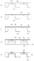
도 1은 본 발명의 전기 접속 구조의 여러가지 형상을 예시한 도면.
도 2는 본 발명의 일실시예에 따른 암접속구조의 제조 과정을 순차적으로 나타낸 도면.
도 3은 본 발명의 제1실시예에 따른 수접속구조의 제조 과정을 순차적으로 나타낸 도면.
도 4는 본 발명의 제2실시예에 따른 수접속구조의 제조 과정을 순차적으로 나타낸 도면.
도 5는 본 발명의 제3실시예에 따른 수접속구조의 제조 과정을 순차적으로 나타낸 도면.
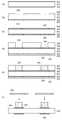
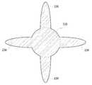
도 6 및 7은 본 발명의 일 실시예에 따른 착탈형 전기 접속 구조의 단면도.
도 8은 도 6 및 7에 도시된 컬럼 및 탄성 핀의 평면도.BRIEF DESCRIPTION OF THE DRAWINGS FIG. 1 illustrates various shapes of the electrical connection structure of the present invention. FIG.
[0001] The present invention relates to a method of manufacturing a female connection structure.
3 is a view sequentially illustrating a manufacturing process of the water connection structure according to the first embodiment of the present invention;
4 is a view sequentially illustrating a manufacturing process of a water connection structure according to a second embodiment of the present invention;
5 is a view sequentially showing a manufacturing process of the water connection structure according to the third embodiment of the present invention.
6 and 7 are cross-sectional views of a removable electrical connection structure according to an embodiment of the invention.
8 is a top view of the column and elastic pins shown in Figs. 6 and 7;
본 명세서에 개시되는 전기 접속 구조는 각종 휴대 전화, 디스플레이 장치 등 각종 전자기기에 적용되는 회로기판 간의 전기 접속, 회로기판에 실장된 전자 부품간의 전기 접속, 회로기판과 전자 부품간의 전기 접속을 위한 구조를 모두 포괄하는 개념이다. 이러한 전기 접속 구조는 각종 휴대 전화, 디스플레이 장치 등 각종 전자기기에 적용 가능하며, 이러한 경우 전자기기의 외관을 구성하는 하우징 내에 본 발명의 전기 접속 구조가 구비될 수 있다. 그 일 예로서 하우징에 내장되는 회로기판과 그에 실장되는 전자 부품과의 전기 접속 구조를 들 수 있을 것이다.The electrical connection structure disclosed in the present specification can be applied to various types of electronic devices such as cellular phones, display devices, and the like, electrical connections between circuit boards, electrical connections between electronic components mounted on circuit boards, and electrical connections between circuit boards and electronic components . Such an electrical connection structure can be applied to various electronic apparatuses such as various portable telephones and display apparatuses. In this case, the electrical connection structure of the present invention can be provided in a housing constituting the appearance of the electronic apparatus. An example of such a structure is an electrical connection structure between a circuit board built in a housing and an electronic component mounted on the circuit board.
이하, 본 발명과 관련된 착탈형 전기 접속 구조에 대하여 도면을 참조하여 보다 상세하게 설명한다.Hereinafter, a detachable electrical connection structure according to the present invention will be described in detail with reference to the drawings.
도 6 및 7은 본 발명의 일 실시예에 따른 전기 접속 구조의 단면도이다.6 and 7 are cross-sectional views of an electrical connection structure according to an embodiment of the present invention.
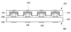
도 6 및 7을 참조하면, 본 발명에 따른 전기 접속 구조는 서로 암수 구조에 의해 결합되는 암접속구조(100) 및 수접속구조(200)를 포함한다. 도 6은 암접속구조(100)와 수접속구조(200)가 분리된 상태를 보이고 있고, 도 7은 암접속구조(100)와 수접속구조(200)가 결합된 상태를 보이고 있다.6 and 7, an electrical connection structure according to the present invention includes a
암접속구조(100)와 수접속구조(200)는 회로기판 자체에 구성될 수도 있고 회로기판에 실장되는 단독 부품일 수 있다. 예를 들어, 암접속구조(100) 또는 수접속구조(200)는 능동소자, 수동소자, 커넥터, 반도체 패키지에 적용되는 인터포저, 반도체 칩 패키지, 3D 적층구조 형태의 반도체 칩 및 패키지, 그리고 적층 세라믹 커패시터(Multilayered Ceramic Capacitor) 중 적어도 어느 하나를 포함할 수 있다.The
암접속구조(100)는 삽입홀(113)이 형성된 암연결부재(110)와, 삽입홀(113)에 구비되는 내부 도전체(120)를 포함한다.The
암연결부재(110)와 절연성 재질 또는 절연성 재질과 도전성 재질의 조합으로 형성될 수 있다. 암연결부재(110)의 재질로 세라믹, 폴리머, 실리콘, 글라스, 메탈 등의 재질 중 하나 또는 하나 이상의 조합을 들 수 있다.And may be formed of a combination of an insulating material or an insulating material and an electrically conductive material with the
내부 도전체(120)는 암연결부재(110)에 형성된 삽입홀(113)의 내벽에 구비된다. 본 실시예에 따르면 삽입홀(113)은 암연결부재(110)의 일면(도 1 및 2에 따르면 하면)으로부터 일정 깊이만큼 리세스된 형태를 가지며, 원통의 형태로 리세스된 형태를 가질 수 있다. 다만 삽입홀(113)은 이러한 형태뿐 아니라 암연결부재(110)를 완전히 관통하는 관통홀의 형태를 갖는 것도 가능하다.The
내부 도전체(140)는 삽입홀(113)의 내측벽 상에 일정 두께만큼 적층된 형태를 가질 수 있다. 본 실시예에 따르면 내부 도전체(140)는 삽입홀(113)의 내측벽의 둘레를 따라 형성되어 있다.The inner conductor 140 may have a predetermined thickness stacked on the inner wall of the
수접속구조(200)는 수연결부재(210)와, 수연결부재(210)로부터 돌출 형성된 컬럼(Colume, 220)과, 컬럼(220)으로부터 외곽 방향으로 연장되는 탄성 핀(Elastic Fin, 230)을 포함한다.The
수연결부재(210)는 암연결부재(110)와 마찬가지로 절연성 재질 또는 절연성 재질과 도전성 재질의 조합으로 형성될 수 있다.The male connecting
컬럼(220)은 도전성 재질을 포함하는 구조로서 수연결부재(210)로부터 돌출되는 구조를 갖는다. 본 실시예의 경우 컬럼(150)이 수연결부재(210)의 회로패턴과 연결된 패드(240)에 실장된 것을 예시하고 있다.The
컬럼(220)은 그 자체가 도전성 재질로 형성되거나, 외부만 도전성 재질로 형성되고 내부는 비도전성 재질로 형성될 수 있다. 후자의 경우의 일예로서 컬럼(220)의 내부가 폴리머, 실리콘, 글라스 등의 재질로 형성되고, 외부만 도전성 재질로 형성될 수 구조를 들 수 있다. 컬럼(220)은 도 7의 도시와 같이 암연결부재(110)와 수연결부재(210)의 대면시 암연결부재(110)의 삽입홀(113)에 삽입되는 구성을 갖는다.The
내부 도전체(120)와 컬럼(220)은 암연결부재(110)와 수연결부재(210) 상에 어레이 형태로 배열될 수 있다. 예를 들어 소정의 행과 열을 갖는 매트릭스 형태 및 그 밖에 다양한 형태로 배열 가능하다.The
도 8 도 6 및 7에 도시된 컬럼(220) 및 탄성 핀(230)의 평면도이다.8 is a top view of the
탄성 핀(230)은 도전성 재질의 표면을 가지며, 컬럼(220)의 외곽 방향으로 연장되는 구조를 갖는다. 탄성 핀(230)은 컬럼(220)이 삽입홀(113)에 삽입될 때 탄성 변형되어 내부 도전체(120)에 탄력적으로 접촉하는 구성을 갖는다.The
탄성 핀(230)은 컬럼(220)이 삽입홀(113)에 삽입될 때 컬럼(220)의 삽입 방향과 반대 방향으로 구부러지도록 구성될 수 있으며, 이는 컬럼(220)과 일체형 구조를 갖거나 컬럼(220)의 상부에 별도의 레이어로서 적층되는 형태의 구성을 가질 수도 있다.The
탄성 핀(230)은 탄성 변형 가능한 도전성 재질(예를 들면, 금속 재질)로 형성되거나, 탄성 변형 가능한 탄성체(고분자, Fiber 등)의 표면에 도전체(예를 들면, 금속)가 코팅되어 형성될 수 있다.The
탄성 핀(230)은 내부 도전체(140)의 복수의 개소와 접촉하도록 복수의 개수를 갖는 것이 바람직하며, 도 3과 같이 컬럼(150)의 외주 방향을 따라 일정 각도만큼 이격되도록 복수로 배열되는 형태를 가질 수 있다. 도 8은 4개의 탄성 핀(230)이 90도의 각도로 배열된 구조를 예시하고 있으나, 탄성 핀(230)의 개수와 형태는 다양하게 변형 실시 가능하다. 예를 들어 탄성 핀(230)은 복수의 개수뿐 아니라 링 형태(환상)로서 단일의 개수를 갖는 것도 가능하다.The
암연결부재(110)와 수연결부재(210)는 제1접속부와 제2접속부를 각각 구비하며, 이들은 각각 복수의 개수를 가질 수 있다. 본 명세서의 제1접속부와 제2접속부는 암연결부재(110)와 수연결부재(120)의 연결에 의해 서로 전기적으로 연결되는 대상을 지칭하며, 그 예로서 패드, 회로패턴, 범프(Bump), 솔더볼(Solder Ball), 비아홀(Via Hole) 등을 들 수 있다.The
본 실시예에 따르면 제1접속부의 일 예로서 암연결부재(110)의 상면에 형성된 패드(130)가 예시되어 있으며, 제2접속부의 일 예로서 수연결부재(210) 하면의 패드(250)가 예시되어 있다.According to the present embodiment, as an example of the first connecting portion, a
내부 도전체(140)는 도전성 재질(예를 들어 금속 재질)로서 제1접속부와 전기적으로 연결되며, 도 1 및 2의 내부 도전체(140)가 삽입홀(113)의 바닥 부분을 통해 암연결부재(110)를 관통하여 패드(111)와 연결된 것을 예시하고 있다.The inner conductor 140 is electrically connected to the first connection portion as a conductive material (e.g., a metal material), and the inner conductor 140 of FIGS. 1 and 2 is connected through a bottom portion of the
컬럼(220)은 수연결부재(210)의 제2접속부와 전기적으로 연결되며, 수연결부재(210) 하면의 패드(250)는 수연결부재(210) 상면의 패드(240)와 비아홀과 같은 도통 구조를 통해 전기적으로 연결될 수 있다.The
이하에서는 본 발명의 전기 접속 구조의 작동 상태에 대하여 설명하기로 한다.Hereinafter, an operation state of the electrical connection structure of the present invention will be described.
도 6과 같이 암접속구조(100)와 수접속구조(200)가 분리된 상태에서 도 7과 같이 수연결부재(210)의 컬럼(220)을 암연결부재(110)의 삽입홀(113)에 삽입하여 암접속구조(100)와 수접속구조(200)를 결합시킬 수 있다. 컬럼(220)이 삽입홀(113)에 삽입되는 과정에서 탄성 핀(230)은 삽입홀(113)의 내벽에 구비된 내부 도전체(120)에 의해 눌러져 탄성 핀(230)에 탄성 변형이 발생하게 되며, 이로 인해 탄성 핀(230)에 발생하는 복원력에 의해 탄성 핀(230)은 내부 도전체(120)에 탄력적으로 접촉하게 된다. 이러한 탄성 복원력은 암연결부재(110)와 수연결부재(210) 사이의 결합력으로 작용하여 암연결부재(110)와 수연결부재(210)가 임의로 분리되지 않도록 한다.The
한편 암연결부재(110)의 제1접속부에 전기적으로 연결된 내부 도전체(220)에 수연결부재(210)의 제2접속부에 전기적으로 연결된 탄성 핀(230)이 접촉함에 따라 제1접속부와 제2접속부 사이의 전기적 연결이 가능하게 되는 것이다.Meanwhile, since the
이와 같이 전기적 접속 구조와 물리적 결합 구조를 함께 구현하여 별도의 물리적 결합 구조를 두지 않아도 되며, 전기 접속 구조를 암연결부재(110)의 내부의 수평 방향의 접촉 형태로 구현하여 전기 접속 구조의 전체 두께를 줄일 수 있는 이점이 있다. 또한 전기 접속 구조를 높이가 낮고 직선에 가까운 구조로 구현하여 전기적 신호전달 속도를 증대시키고, 신호 손실을 줄여 신호품질을 향상시킬 수 있는 이점이 있다.As described above, the electrical connection structure and the physical connection structure are implemented together, so that there is no need to provide a separate physical connection structure. The electrical connection structure can be realized in a horizontal contact form inside the
한편, 이상에서는 수접속구조(200)의 구조로서 컬럼(220)의 외곽에 탄성 핀(240)이 구비된 구조인 것으로만 설명하였으나, 탄성 핀(240)이 구비되지 않고 컬럼(220)이 삽입홀(113)에 끼움 결합되어 컬럼(220)이 직접 내부 도전체(220)에 접촉하는 구조도 가능하다 할 것이다.Although the
이하, 도 2 내지 5를 참조하여 본 발명의 일 실시예에 따른 전기 접속 구조의 제조 방법에 대하여 설명하기로 한다.Hereinafter, a method of manufacturing an electrical connection structure according to an embodiment of the present invention will be described with reference to FIGS.
본 발명에 따른 전기 접속 구조의 제조 방법은 암연결부재(110) 및 수연결부재(210)로 사용될 절연부재(101,201)를 마련하는 단계와, 포토리소그래피 공정을 이용하여 각 절연부재(101,201) 상에 도전체를 패터닝하여 내부 도전체(120) 및 컬럼(220)을 형성하는 단계를 포함한다.The method for manufacturing an electrical connection structure according to the present invention includes the steps of providing insulating
이하에서는 암접속구조(100)와 수접속구조(200) 각각의 제조과정에 대하여 상세히 살펴보기로 한다.Hereinafter, the manufacturing process of each of the
도 2는 본 발명의 일실시예에 따른 암접속구조의 제조 과정을 순차적으로 나타낸 도면이다.FIG. 2 is a view sequentially illustrating the manufacturing process of the female connection structure according to an embodiment of the present invention.
도 2의 (a)와 같이 암연결부재(110)로 사용될 절연부재(101)를 마련하고, 절연부재(101)에 삽입홀(113)을 형성한다. 이 때 패드(130)와 내부 도전체(120) 사이의 도통을 위한 토통홀(115)을 함께 가공할 수 있다.An insulating
그리고 (b)와 같이 전극층(102)을 적층한다. 전극층(102)으로 구리와 같은 도전체 필름이 사용될 수 있으며, 이는 전기 도금시 전극 인가를 위한 구조로 사용된다.Then, the
다음으로 (c)와 같이 드라이필름(104)을 적층하고, 포토리소그래피 공정을 통해 드라이필름(104)에 삽입홀(113)에 대응되는 패턴홀(123)을 형성한다. 드라이필름(104)에 패턴홀(123)을 미리 형성하고, 이를 절연부재(101)에 부착하는 것도 가능하다.Next, a
이 때 삽입홀(113)의 반대측에 다른 드라이필름(104)을 부착하고, 포토리소그래피 공정을 통해 패드(130)에 대응되는 패턴홀(133)을 형성할 수 있다. 각 패턴홀(123,133)의 형성을 위한 포토리소그래피 공정은 동시에 진행될 수 있다.At this time, another
다음으로 (d)와 같이 전기 도금을 통해 삽입홀(123) 내에 구리와 같은 도전물질(125)을 충전시킨다. 이 때 이와 동시에 삽입홀(123) 반대쪽의 패턴홀(133) 내에도 도전 물질(135)을 충전시킬 수 있다. 이와 같이 삽입홀(123)과 그 반대쪽의 패턴홀(133) 내의 전기 도금을 함께 수행하여 내부 도전체(120)를 위한 구조와 패드(130)를 위한 구조를 함께 형성할 수 있다.Next, the
다음으로 (e)와 같이 삽입홀(123) 내의 도전 물질(125)을 기계적 또는 화학적으로 에칭하여 내부 도전체(120)의 형상을 형성한다. 아울러 드라이필름(102,104)을 박리하고, 전극층(102)의 일부를 기계적 또는 화학적 에칭을 통해 제거하여 암접속구조(100)가 최종적으로 완성된다.Next, the
도 3은 본 발명의 제1실시예에 따른 수접속구조의 제조 과정을 순차적으로 나타낸 도면이다.FIG. 3 is a view sequentially illustrating the manufacturing process of the connection structure according to the first embodiment of the present invention.
도 3의 (a)와 같이 수연결부재(210)로 사용될 절연부재(201)를 마련하고, 절연부재(201)의 일면에 전극층(202)을 적층한다. 본 실시예의 경우 반대쪽 패드(250)의 형성을 위해 절연부재(202)의 타면에도 전극층(203)을 형성하였다. 이 과정에서 절연부재(201) 상하면의 회로 도통을 위한 비아홀 등의 구조를 형성하는 것도 가능하다.An insulating
그리고 (b)와 같이 전극층(202,203)의 외곽에 드라이필름(204,205)를 적층하고, 포토리소그래피 공정을 통해 각 드라이필름(204,205)에 패드(240,250)의 형성을 위한 패턴홀(243,253)을 형성한다.
그리고 (c)와 같이 각 드라이필름(204,205)의 패턴홀(232,253)에 구리와 같은 도전물질을 충전하여 패드(240,250)를 형성한다. 이 때 패드(240,250) 사이를 도통하기 위한 비아홀 내에도 전기 도금을 수행할 수 있다.As shown in (c), the pattern holes 232 and 253 of the respective
다음으로 (d)와 같이 컬럼(220)을 형성할 부분과 그렇지 않은 부분 양쪽에 드라이필름(206,207)을 적층한다. 그리고 컬럼(220)을 형성할 위치의 드라이필름(206)에 컬럼홀(223)을 형성한다. 컬럼홀(223) 또한 앞서 설명된 패턴홀(234,253)과 마찬가지로 포토리소그래피 공정에 의해 형성한다. 컬럼(220)이 형성된 위치와 반대쪽의 드라이필름(207)은 더 이상 전기 도금이 진행되지 않도록 배리어로서의 기능을 한다.Next, as shown in (d), the
다음으로 (e)와 같이 전기 도금을 통해 컬럼홀(223) 내에 구리와 같은 도전 물질을 충전하여 컬럼(225)의 구조를 형성한다. 수접속구조(200)에 탄성 핀(230)을 형성할 필요가 없을 경우, 드라이필름(204,205,206,207)을 박리하고, 전극층(202,203)의 불필요한 부분을 제거하면 수접속구조(200)가 완성된다. 이하의 공정은 탄성 핀(230)을 형성하기 위한 공정이다.Next, a conductive material such as copper is filled in the
(f)와 같이 컬럼(220)을 위한 도전물질(225)을 덮도록 드라이필름(208)을 적층하고, 포토리소그래피 공정을 통해 드라이필름(208)에 탄성 핀(230)에 대응되는 형태의 패턴홀(233)을 형성한다.the
그리고 (g)와 같이 전기 도금을 통해 패턴홀(233) 내에 구리 등의 도전 물질을 충전하여 탄성 핀(230)의 구조를 형성한다. 그리고 (h)와 같이 드라이필름(204,205,206,207,208)을 박리하고, 기계적 또는 화학적 에칭을 통해 전극층(202,203)의 불필요한 부분을 제거하여 수접속구조(200)를 최종적으로 완성할 수 있다.Then, conductive material such as copper is filled in the
도 4는 본 발명의 제2실시예에 따른 수접속구조의 제조 과정을 순차적으로 나타낸 도면이다.4 is a view sequentially illustrating a manufacturing process of the water connection structure according to the second embodiment of the present invention.
본 실시예의 수접속구조는 탄성 핀(230)을 형성하는 공정을 제외하고 앞선 실시예와 동일하다. 즉, 도 4의 (a) 단계부터 (e) 단계는 도 3의 (a) 단계부터 (e) 단계까지와 동일하다.The water connection structure of this embodiment is the same as the previous embodiment except for the process of forming the
본 실시예의 수접속구조 제조방법은 컬럼(220)을 형성하는 단계까지는 동일하되, 그 이후에 (f)와 같이 별도로 제작된 탄성 핀(230)울 컬럼(220)에 적층하여 제작하는 점에 특징이 있다.The manufacturing method of the water connection structure of the present embodiment is characterized in that the steps up to the step of forming the
도 5는 본 발명의 제3실시예에 따른 수접속구조의 제조 과정을 순차적으로 나타낸 도면이다.FIG. 5 is a view sequentially illustrating the manufacturing process of the connection structure according to the third embodiment of the present invention.
본 실시예에 따른 수접속구조의 제조방법은 앞선 실시예들과 역순으로 탄성 핀(230)으로 사용될 금속판(301)에 컬럼(220)과 절연부재(210)를 순차적으로 적층하는 방식으로 이루어진다.The manufacturing method of the water connection structure according to the present embodiment is performed in such a manner that the
도 5의 (a)와 같이 탄성 핀(230)으로 사용될 금속판(301)을 마련하고 금속판(301)의 양면에 드라이필름(302,303)을 적층한다.A
그리고 (b)와 같이 한 쪽 드라이필름(302)에 포토리소그래피 공정을 통해 컬럼(220)에 대응되는 컬럼홀(323)을 형성하고, (c)와 같이 전기 도금을 통해 컬럼홀(323) 내에 구리와 같은 도전물질(325)을 충전시켜 컬럼(220) 구조를 형성한다.A
그리도 (e)와 같이 드라이필름(304)을 적층하고 드라이필름(304)에 패드(240)의 형성을 위한 패턴홀(343)을 형성한다. 다음으로 패턴홀(343) 내에 도전물질(345)을 충전하여 패드(240)를 형성한다.A
그리고 (f)와 같이 수연결부재(210)로 사용될 절연부재(210)를 적층한다. 절연부재(210)에는 패드(250)로 사용될 금속층(306)이 추가로 적층될 수 있으며, 이후 비아홀 가공 및 그 도통을 위한 도금 공정 등이 추가로 수행될 수 있다.Then, the insulating
다음으로 포토리스그래피 공정을 통해 금속판(302) 및 금속층(306)을 패터닝하여 탄성 핀(230) 및 패드(250)를 형성하고, 드라이필름(302,303,304)를 제거하면 (g)와 같이 수접속구조가 완성되는 것이다.Next, the
도 1은 본 발명의 전기 접속 구조의 여러가지 형상을 예시한 도면이다.BRIEF DESCRIPTION OF DRAWINGS FIG. 1 is a view illustrating various shapes of an electrical connection structure of the present invention. FIG.
도 1은 회로기판(10)에 다양한 형태의 전기 접속 구조(A 내지 D)가 실장된 것을 예시하고 있다. 이상과 같이 인쇄회로기판 제조방법을 이용하여 전기 접속 구조를 제작할 경우, 암연결부재(110) 또는 수연결부재(120)를 다양한 형태로 제작할 수 있으며, 이에 따라 디자인을 용이하게 변경할 수 있다. 이에 따라 실장 위치의 자유도를 증대시키고, 공간 활용의 효율성을 향상시킬 수 있는 것이다.FIG. 1 illustrates mounting of various types of electrical connection structures A to D on a
예를 들어 D 구조와 같이 나사홀(15)의 배치 공간을 피할 수 있도록 디자인 하는 것이 가능하다 할 것이다.For example, it is possible to design such that the arrangement space of the screw holes 15 can be avoided like the D structure.
나아가 도 1에 나타난 A 구조에 대한 확대도면과 같이, 내부 도전체(120) 또는 컬럼(220)이 암연결부재(110) 또는 수연결부재(120)에 다양한 형태로 배열할 수 있는 이점이 있다.The
이상에서 설명한 본 발명과 관련된 전기 접속 구조 및 그 제조 방법은 전기 접속용 커넥터, 반도체 패키지 조립체, 플립 칩의 상호 접속 구조, MLCC (Multi Layer Ceramic Capacitor)의 커패시터와 다른 소자(또는 기판)의 상호 접속 구조 등 다양한 분야에 적용 가능하다.The above-described electrical connection structure and its manufacturing method according to the present invention can be applied to an electrical connection connector, a semiconductor package assembly, a flip chip interconnection structure, an interconnection of a capacitor of an MLCC (Multi Layer Ceramic Capacitor) Structure and so on.
한편 이상에서 설명한 전기 접속 구조 및 그 제조 방법은 위에서 설명된 실시예들의 구성과 방법에 한정되는 것이 아니라, 상기 실시예들은 다양한 변형이 이루어질 수 있도록 각 실시예들의 전부 또는 일부가 선택적으로 조합되어 구성될 수 있으며, 본 발명의 기술사상의 범위 내에서 당업자에 의해 다양한 변형이 이루어질 수 있다.
It should be noted that the above-described electrical connection structure and the method of manufacturing the same are not limited to the configurations and methods of the embodiments described above, but the embodiments may be modified so that all or some of the embodiments are selectively combined And various modifications may be made by those skilled in the art within the scope of the technical idea of the present invention.
Claims (9)
Translated fromKorean상기 암연결부재 및 수연결부재로 사용될 절연부재를 마련하는 단계; 및
포토리소그래피 공정을 이용하여 상기 각 절연부재 상에 도전체를 패터닝하여 상기 내부 도전체 및 컬럼을 형성하는 단계를 포함하고,
상기 암접속구조의 제조 단계는,
상기 절연부재에 상기 삽입홀을 형성하는 단계;
상기 절연부재에 전극층 및 제1드라이필름을 적층하는 단계;
포토리소그래피 공정을 통해 상기 제1드라이필름에 상기 삽입홀에 대응되는 형태의 패턴홀을 형성하는 단계; 및
전기 도금을 통해 상기 삽입홀 내에 도전 물질을 충전하는 단계;
상기 삽입홀 내의 도전 물질을 에칭하여 상기 내부 도전체를 형성하는 단계를 포함하는 것을 특징으로 하는 전기 접속 구조의 제조 방법.A female connection structure in which an inner conductor is provided in an insertion hole of the female connection member; and a connection structure in which a conductive column inserted into the insertion hole and in contact with the inner conductor protrudes from the male connection member, In the production method of the present invention,
Providing an insulating member to be used as the female connecting member and the male connecting member; And
And patterning the conductor on each of the insulating members using a photolithography process to form the internal conductor and the column,
The step of manufacturing the female connection structure includes:
Forming the insertion hole in the insulating member;
Depositing an electrode layer and a first dry film on the insulating member;
Forming a pattern hole corresponding to the insertion hole in the first dry film through a photolithography process; And
Filling the conductive material in the insertion hole through electroplating;
And etching the conductive material in the insertion hole to form the internal conductor.
상기 내부 도전체의 형성을 위한 전기 도금시 상기 내부 도전체와 연결되는 패드의 형성을 위한 구조를 함께 전기 도금하는 것을 특징으로 하는 전기 접속 구조의 제조 방법.3. The method of claim 2,
Wherein a structure for forming a pad connected to the inner conductor is electroplated together when electroplating for forming the inner conductor is performed.
상기 암연결부재 및 수연결부재로 사용될 절연부재를 마련하는 단계; 및
포토리소그래피 공정을 이용하여 상기 각 절연부재 상에 도전체를 패터닝하여 상기 내부 도전체 및 컬럼을 형성하는 단계를 포함하고,
상기 수접속구조의 제조 단계는,
상기 절연부재에 전극층 및 제2드라이필름을 적층하는 단계;
포토리소그래피 공정을 통해 제2드라이필름에 컬럼홀을 형성하는 단계; 및
전기 도금을 통해 상기 컬럼홀 내에 도전 물질을 충전하여 상기 컬럼을 형성하는 단계를 포함하는 것을 특징으로 하는 전기 접속 구조의 제조 방법.A female connection structure in which an inner conductor is provided in an insertion hole of the female connection member; and a connection structure in which a conductive column inserted into the insertion hole and in contact with the inner conductor protrudes from the male connection member, In the production method of the present invention,
Providing an insulating member to be used as the female connecting member and the male connecting member; And
And patterning the conductor on each of the insulating members using a photolithography process to form the internal conductor and the column,
Wherein the step of fabricating the water-
Depositing an electrode layer and a second dry film on the insulating member;
Forming a column hole in the second dry film through a photolithography process; And
And filling the conductive material in the column hole through electroplating to form the column.
상기 제2드라이필름의 적층 전, 상기 절연부재의 양측에 제3 및 제4드라이필름을 적층하는 단계;
포토리소그래피 공정을 통해 제3 및 제4드라이필름에 패드 형성을 위한 패턴홀을 형성하는 단계; 및
전기 도금을 통해 상기 제3 및 제4드라이필름의 패턴홀에 도전 물질을 충전하여 패드를 형성하는 단계를 더 포함하는 것을 특징으로 하는 전기 접속 구조의 제조 방법.5. The method of claim 4,
Laminating third and fourth dry films on both sides of the insulating member before stacking the second dry film;
Forming pattern holes for forming pads on the third and fourth dry films through a photolithography process; And
Further comprising the step of filling the pattern holes of the third and fourth dry films with a conductive material through electroplating to form a pad.
상기 컬럼을 덮도록 제5드라이필름을 적층하는 단계;
포토리소그래피 공정을 통해 제5드라이필름에 탄성 핀에 대응되는 형태의 패턴홀을 형성하는 단계; 및
전기 도금을 통해 상기 제5드라이필름의 패턴홀 내에 도전 물질을 충전하여 탄성 핀을 형성하는 단계를 더 포함하는 것을 특징으로 하는 전기 접속 구조의 제조 방법.5. The method of claim 4,
Laminating a fifth dry film to cover the column;
Forming a pattern hole corresponding to the elastic pin on the fifth dry film through a photolithography process; And
Further comprising the step of filling the pattern holes of the fifth dry film with a conductive material through electroplating to form elastic fins.
상기 컬럼에 별도로 제작된 탄성 핀을 적층하는 단계를 더 포함하는 것을 특징으로 하는 전기 접속 구조의 제조 방법.5. The method of claim 4,
Further comprising the step of laminating elastic pins separately manufactured in said column.
상기 암접속구조의 제조단계는,
상기 암연결부재로 사용될 절연부재를 마련하는 단계; 및
포토리소그래피 공정을 이용하여 상기 각 절연부재 상에 도전체를 패터닝하여 상기 내부 도전체를 형성하는 단계를 포함하고,
상기 수접속구조의 제조 단계는,
상기 탄성 핀으로 사용될 금속판을 마련하는 단계;
포토리소그래피 공정 및 도금 공정을 이용하여 상기 금속판에 상기 컬럼을 형성하는 단계;
상기 컬럼에 상기 수연결부재로 사용될 절연부재를 적층하는 단계; 및
상기 금속판을 패터닝하여 상기 탄성핀을 형성하는 단계를 포함하는 것을 특징으로 하는 전기 접속 구조의 제조 방법.A female connection structure in which an inner conductor is provided in an insertion hole of the female connection member; and a conductive column which is inserted and fixed in the insertion hole is protruded from the male connection member and has elastic pins in contact with the inner conductor in the column A method of manufacturing an electrical connection structure including a water connection structure,
The step of manufacturing the female connection structure includes:
Providing an insulating member to be used as the female connecting member; And
And patterning the conductor on each of the insulating members using a photolithography process to form the internal conductor,
Wherein the step of fabricating the water-
Providing a metal plate to be used as the elastic pin;
Forming the column on the metal plate using a photolithography process and a plating process;
Stacking an insulating member to be used as the male connecting member in the column; And
And patterning the metal plate to form the elastic pin.
상기 암연결부재 또는 수연결부재는 능동소자, 수동소자, 전기 접속용 커넥터, 반도체 칩 패키지, 반도체 패키지에 적용되는 인터포저, 3D 적층구조 형태의 반도체 칩 및 패키지, 및 적층 세라믹 커패시터(Multilayered Ceramic Capacitor) 중 적어도 어느 하나를 포함하는 것을 특징으로 하는 전기 접속 구조의 제조 방법.
9. The method according to any one of claims 2 to 8,
The arm connection member or the male connection member may include at least one of an active element, a passive element, an electrical connection connector, a semiconductor chip package, an interposer applied to a semiconductor package, a semiconductor chip and package in the form of a 3D stacked structure, and a multilayered ceramic capacitor ). ≪ / RTI >
Priority Applications (6)
| Application Number | Priority Date | Filing Date | Title |
|---|---|---|---|
| KR1020150010482AKR101689547B1 (en) | 2015-01-22 | 2015-01-22 | Method for manufacturing electrical interconnection structure |
| PCT/KR2015/002753WO2016117761A1 (en) | 2015-01-22 | 2015-03-20 | Method for manufacturing electrical connection structure |
| CN201580074096.9ACN107210554A (en) | 2015-01-22 | 2015-03-20 | Method for manufacturing electric interconnection structure |
| JP2017539360AJP2018512694A (en) | 2015-01-22 | 2015-03-20 | Manufacturing method of electrical connection structure |
| US15/545,703US20180013251A1 (en) | 2015-01-22 | 2015-03-20 | Method for manufacturing electrical interconnection structure |
| TW104140417ATW201640973A (en) | 2015-01-22 | 2015-12-02 | Method for manufacturing electrical interconnection structure |
Applications Claiming Priority (1)
| Application Number | Priority Date | Filing Date | Title |
|---|---|---|---|
| KR1020150010482AKR101689547B1 (en) | 2015-01-22 | 2015-01-22 | Method for manufacturing electrical interconnection structure |
Publications (2)
| Publication Number | Publication Date |
|---|---|
| KR20160090549A KR20160090549A (en) | 2016-08-01 |
| KR101689547B1true KR101689547B1 (en) | 2016-12-26 |
Family
ID=56417277
Family Applications (1)
| Application Number | Title | Priority Date | Filing Date |
|---|---|---|---|
| KR1020150010482AExpired - Fee RelatedKR101689547B1 (en) | 2015-01-22 | 2015-01-22 | Method for manufacturing electrical interconnection structure |
Country Status (6)
| Country | Link |
|---|---|
| US (1) | US20180013251A1 (en) |
| JP (1) | JP2018512694A (en) |
| KR (1) | KR101689547B1 (en) |
| CN (1) | CN107210554A (en) |
| TW (1) | TW201640973A (en) |
| WO (1) | WO2016117761A1 (en) |
Families Citing this family (7)
| Publication number | Priority date | Publication date | Assignee | Title |
|---|---|---|---|---|
| US11444049B2 (en) | 2017-08-14 | 2022-09-13 | Sony Corporation | Electronic component module, method for producing the same, endoscopic apparatus, and mobile camera |
| KR102421521B1 (en)* | 2018-01-31 | 2022-07-15 | 삼성전자주식회사 | Electronic device including connector with stacked structure |
| JP7269347B2 (en) | 2018-08-22 | 2023-05-08 | リキッド ワイヤ インコーポレイテッド | Structures with deformable conductors |
| CN110797686A (en)* | 2019-01-30 | 2020-02-14 | 广州方邦电子股份有限公司 | Integrated device |
| CN110228091A (en)* | 2019-05-31 | 2019-09-13 | 四川省银丰食品有限公司 | A kind of rice flour automation feeding cutting system |
| CN115696888A (en)* | 2021-07-22 | 2023-02-03 | 启碁科技股份有限公司 | Shield structure and manufacturing method thereof |
| CN117452734B (en)* | 2023-12-26 | 2024-03-26 | 东莞市钜欣电子有限公司 | Electrochromic film, camera module and electronic equipment |
Citations (2)
| Publication number | Priority date | Publication date | Assignee | Title |
|---|---|---|---|---|
| JP2001057378A (en)* | 1999-06-28 | 2001-02-27 | Advantest Corp | Manufacture for contact structure |
| JP2003323924A (en)* | 2002-04-30 | 2003-11-14 | Molex Inc | Connector for board connection |
Family Cites Families (10)
| Publication number | Priority date | Publication date | Assignee | Title |
|---|---|---|---|---|
| TW381328B (en)* | 1994-03-07 | 2000-02-01 | Ibm | Dual substrate package assembly for being electrically coupled to a conducting member |
| TW407386B (en)* | 1998-01-05 | 2000-10-01 | Jaybis Co Ltd | Multiple cores substrate and pair substrate connector |
| US6031282A (en)* | 1998-08-27 | 2000-02-29 | Advantest Corp. | High performance integrated circuit chip package |
| JP4710627B2 (en)* | 2006-01-26 | 2011-06-29 | パナソニック電工株式会社 | Board to board connector |
| JP4936457B2 (en)* | 2007-04-24 | 2012-05-23 | パナソニック株式会社 | Bump structure and manufacturing method thereof |
| JP5030218B2 (en)* | 2007-07-10 | 2012-09-19 | 矢崎総業株式会社 | Press-fit terminal |
| JP2010033714A (en)* | 2008-07-24 | 2010-02-12 | Kyocera Elco Corp | Connector |
| JP5366706B2 (en)* | 2009-08-24 | 2013-12-11 | パナソニック株式会社 | Female connector for board connection and connector assembly including the same |
| JP5908225B2 (en) | 2011-07-06 | 2016-04-26 | 第一電子工業株式会社 | Electrical connector |
| JP5781991B2 (en)* | 2012-08-07 | 2015-09-24 | 京セラコネクタプロダクツ株式会社 | connector |
- 2015
- 2015-01-22KRKR1020150010482Apatent/KR101689547B1/ennot_activeExpired - Fee Related
- 2015-03-20JPJP2017539360Apatent/JP2018512694A/enactivePending
- 2015-03-20CNCN201580074096.9Apatent/CN107210554A/enactivePending
- 2015-03-20USUS15/545,703patent/US20180013251A1/ennot_activeAbandoned
- 2015-03-20WOPCT/KR2015/002753patent/WO2016117761A1/ennot_activeCeased
- 2015-12-02TWTW104140417Apatent/TW201640973A/enunknown
Patent Citations (2)
| Publication number | Priority date | Publication date | Assignee | Title |
|---|---|---|---|---|
| JP2001057378A (en)* | 1999-06-28 | 2001-02-27 | Advantest Corp | Manufacture for contact structure |
| JP2003323924A (en)* | 2002-04-30 | 2003-11-14 | Molex Inc | Connector for board connection |
Also Published As
| Publication number | Publication date |
|---|---|
| CN107210554A (en) | 2017-09-26 |
| JP2018512694A (en) | 2018-05-17 |
| US20180013251A1 (en) | 2018-01-11 |
| TW201640973A (en) | 2016-11-16 |
| WO2016117761A1 (en) | 2016-07-28 |
| KR20160090549A (en) | 2016-08-01 |
Similar Documents
| Publication | Publication Date | Title |
|---|---|---|
| KR101689547B1 (en) | Method for manufacturing electrical interconnection structure | |
| KR101488266B1 (en) | Matable electrical interconnection structure for electrical interconnection, connector, semiconductor package assembly, and electrical device having the same | |
| US9301391B2 (en) | Substrate structure, semiconductor package device, and manufacturing method of substrate structure | |
| TWI479971B (en) | Wiring board, method of manufacturing the same, and semiconductor device having wiring board | |
| US11257765B2 (en) | Chip package structure including connecting posts and chip package method | |
| JP2018046298A (en) | Circuit board and circuit module | |
| US20150062854A1 (en) | Electronic component module and method of manufacturing the same | |
| JP5934154B2 (en) | Substrate structure on which electronic components are mounted and method for manufacturing the same | |
| US20120133030A1 (en) | Tsv substrate structure and the stacked assembly thereof | |
| KR101565690B1 (en) | Circuit board, method for menufacturing of circuit board, electronic component package and method for menufacturing of electronic component package | |
| CN103281858A (en) | Printed circuit board and manufacturing method thereof, and flip-chip packaging member and manufacturing method thereof | |
| KR20170124769A (en) | Electric component module and manufacturing method threrof | |
| TWI595706B (en) | Matable electrical interconnection structure and electronic device having the same | |
| CN104218015A (en) | Encapsulating structure and manufacturing method thereof | |
| CN102280428A (en) | Packaging piece and manufacture method thereof | |
| CN205755064U (en) | Component carrier | |
| JP4479392B2 (en) | Memory module manufacturing method | |
| TWI550745B (en) | Packaging substrate and manufacturing method thereof | |
| KR20110080491A (en) | Semiconductor chip package manufacturing method | |
| KR102248525B1 (en) | Manufacturing method of electric component module | |
| CN116782496A (en) | Connector and manufacturing method | |
| CN119676949A (en) | Board-to-board connection structure and manufacturing method thereof | |
| KR20160067576A (en) | Printed circuit board and manufacturing method method thereof | |
| JPH09186453A (en) | Wiring board manufacturing method and wiring board structure | |
| KR20080026434A (en) | PCB and PCB manufacturing method using printed circuit board, printed circuit board, and manufacturing method of PCB card |
Legal Events
| Date | Code | Title | Description |
|---|---|---|---|
| A201 | Request for examination | ||
| PA0109 | Patent application | St.27 status event code:A-0-1-A10-A12-nap-PA0109 | |
| PA0201 | Request for examination | St.27 status event code:A-1-2-D10-D11-exm-PA0201 | |
| E902 | Notification of reason for refusal | ||
| PE0902 | Notice of grounds for rejection | St.27 status event code:A-1-2-D10-D21-exm-PE0902 | |
| E13-X000 | Pre-grant limitation requested | St.27 status event code:A-2-3-E10-E13-lim-X000 | |
| P11-X000 | Amendment of application requested | St.27 status event code:A-2-2-P10-P11-nap-X000 | |
| P13-X000 | Application amended | St.27 status event code:A-2-2-P10-P13-nap-X000 | |
| PG1501 | Laying open of application | St.27 status event code:A-1-1-Q10-Q12-nap-PG1501 | |
| E701 | Decision to grant or registration of patent right | ||
| PE0701 | Decision of registration | St.27 status event code:A-1-2-D10-D22-exm-PE0701 | |
| GRNT | Written decision to grant | ||
| PR0701 | Registration of establishment | St.27 status event code:A-2-4-F10-F11-exm-PR0701 | |
| PR1002 | Payment of registration fee | St.27 status event code:A-2-2-U10-U11-oth-PR1002 Fee payment year number:1 | |
| PG1601 | Publication of registration | St.27 status event code:A-4-4-Q10-Q13-nap-PG1601 | |
| P22-X000 | Classification modified | St.27 status event code:A-4-4-P10-P22-nap-X000 | |
| PC1903 | Unpaid annual fee | St.27 status event code:A-4-4-U10-U13-oth-PC1903 Not in force date:20191221 Payment event data comment text:Termination Category : DEFAULT_OF_REGISTRATION_FEE | |
| PC1903 | Unpaid annual fee | St.27 status event code:N-4-6-H10-H13-oth-PC1903 Ip right cessation event data comment text:Termination Category : DEFAULT_OF_REGISTRATION_FEE Not in force date:20191221 |