KR101689110B1 - Data shifting - Google Patents
Data shiftingDownload PDFInfo
- Publication number
- KR101689110B1 KR101689110B1KR1020167009805AKR20167009805AKR101689110B1KR 101689110 B1KR101689110 B1KR 101689110B1KR 1020167009805 AKR1020167009805 AKR 1020167009805AKR 20167009805 AKR20167009805 AKR 20167009805AKR 101689110 B1KR101689110 B1KR 101689110B1
- Authority
- KR
- South Korea
- Prior art keywords
- sense
- memory cell
- line
- coupled
- isolation device
- Prior art date
- Legal status (The legal status is an assumption and is not a legal conclusion. Google has not performed a legal analysis and makes no representation as to the accuracy of the status listed.)
- Active
Links
- 230000015654memoryEffects0.000claimsabstractdescription187
- 238000002955isolationMethods0.000claimsabstractdescription146
- 238000000034methodMethods0.000claimsabstractdescription20
- 230000000295complement effectEffects0.000claimsdescription25
- 230000003213activating effectEffects0.000claimsdescription13
- 238000012546transferMethods0.000claimsdescription5
- 230000004913activationEffects0.000claimsdescription2
- 238000012545processingMethods0.000description12
- 238000003491arrayMethods0.000description9
- 239000003990capacitorSubstances0.000description7
- 238000010586diagramMethods0.000description6
- 238000013459approachMethods0.000description3
- 230000001066destructive effectEffects0.000description2
- 238000010304firingMethods0.000description2
- 239000013641positive controlSubstances0.000description2
- 239000004065semiconductorSubstances0.000description2
- 230000006978adaptationEffects0.000description1
- 230000008859changeEffects0.000description1
- 238000004891communicationMethods0.000description1
- 230000008878couplingEffects0.000description1
- 238000010168coupling processMethods0.000description1
- 238000005859coupling reactionMethods0.000description1
- 230000000694effectsEffects0.000description1
- 238000011067equilibrationMethods0.000description1
- 230000005669field effectEffects0.000description1
- 238000007667floatingMethods0.000description1
- 230000002093peripheral effectEffects0.000description1
- 230000002085persistent effectEffects0.000description1
- 230000008569processEffects0.000description1
- 230000000750progressive effectEffects0.000description1
- 230000004044responseEffects0.000description1
- 230000003068static effectEffects0.000description1
Images


Classifications
- G—PHYSICS
- G11—INFORMATION STORAGE
- G11C—STATIC STORES
- G11C7/00—Arrangements for writing information into, or reading information out from, a digital store
- G11C7/06—Sense amplifiers; Associated circuits, e.g. timing or triggering circuits
- G11C7/065—Differential amplifiers of latching type
- G—PHYSICS
- G11—INFORMATION STORAGE
- G11C—STATIC STORES
- G11C11/00—Digital stores characterised by the use of particular electric or magnetic storage elements; Storage elements therefor
- G11C11/21—Digital stores characterised by the use of particular electric or magnetic storage elements; Storage elements therefor using electric elements
- G11C11/34—Digital stores characterised by the use of particular electric or magnetic storage elements; Storage elements therefor using electric elements using semiconductor devices
- G11C11/40—Digital stores characterised by the use of particular electric or magnetic storage elements; Storage elements therefor using electric elements using semiconductor devices using transistors
- G11C11/401—Digital stores characterised by the use of particular electric or magnetic storage elements; Storage elements therefor using electric elements using semiconductor devices using transistors forming cells needing refreshing or charge regeneration, i.e. dynamic cells
- G11C11/4063—Auxiliary circuits, e.g. for addressing, decoding, driving, writing, sensing or timing
- G11C11/407—Auxiliary circuits, e.g. for addressing, decoding, driving, writing, sensing or timing for memory cells of the field-effect type
- G11C11/409—Read-write [R-W] circuits
- G11C11/4091—Sense or sense/refresh amplifiers, or associated sense circuitry, e.g. for coupled bit-line precharging, equalising or isolating
- G—PHYSICS
- G11—INFORMATION STORAGE
- G11C—STATIC STORES
- G11C19/00—Digital stores in which the information is moved stepwise, e.g. shift registers
- G—PHYSICS
- G11—INFORMATION STORAGE
- G11C—STATIC STORES
- G11C5/00—Details of stores covered by group G11C11/00
- G11C5/06—Arrangements for interconnecting storage elements electrically, e.g. by wiring
- G—PHYSICS
- G11—INFORMATION STORAGE
- G11C—STATIC STORES
- G11C7/00—Arrangements for writing information into, or reading information out from, a digital store
- G11C7/06—Sense amplifiers; Associated circuits, e.g. timing or triggering circuits
- G—PHYSICS
- G11—INFORMATION STORAGE
- G11C—STATIC STORES
- G11C7/00—Arrangements for writing information into, or reading information out from, a digital store
- G11C7/06—Sense amplifiers; Associated circuits, e.g. timing or triggering circuits
- G11C7/08—Control thereof
- G—PHYSICS
- G11—INFORMATION STORAGE
- G11C—STATIC STORES
- G11C7/00—Arrangements for writing information into, or reading information out from, a digital store
- G11C7/10—Input/output [I/O] data interface arrangements, e.g. I/O data control circuits, I/O data buffers
- G11C7/1006—Data managing, e.g. manipulating data before writing or reading out, data bus switches or control circuits therefor
- G—PHYSICS
- G11—INFORMATION STORAGE
- G11C—STATIC STORES
- G11C7/00—Arrangements for writing information into, or reading information out from, a digital store
- G11C7/10—Input/output [I/O] data interface arrangements, e.g. I/O data control circuits, I/O data buffers
- G11C7/1015—Read-write modes for single port memories, i.e. having either a random port or a serial port
- G11C7/1036—Read-write modes for single port memories, i.e. having either a random port or a serial port using data shift registers
- G—PHYSICS
- G11—INFORMATION STORAGE
- G11C—STATIC STORES
- G11C7/00—Arrangements for writing information into, or reading information out from, a digital store
- G11C7/22—Read-write [R-W] timing or clocking circuits; Read-write [R-W] control signal generators or management
- G—PHYSICS
- G11—INFORMATION STORAGE
- G11C—STATIC STORES
- G11C8/00—Arrangements for selecting an address in a digital store
- G11C8/10—Decoders
- G—PHYSICS
- G11—INFORMATION STORAGE
- G11C—STATIC STORES
- G11C2207/00—Indexing scheme relating to arrangements for writing information into, or reading information out from, a digital store
- G11C2207/002—Isolation gates, i.e. gates coupling bit lines to the sense amplifier
- G—PHYSICS
- G11—INFORMATION STORAGE
- G11C—STATIC STORES
- G11C2207/00—Indexing scheme relating to arrangements for writing information into, or reading information out from, a digital store
- G11C2207/005—Transfer gates, i.e. gates coupling the sense amplifier output to data lines, I/O lines or global bit lines
Landscapes
- Engineering & Computer Science (AREA)
- Microelectronics & Electronic Packaging (AREA)
- Computer Hardware Design (AREA)
- Dram (AREA)
- Semiconductor Memories (AREA)
Abstract
Translated fromKoreanDescription
Translated fromKorean본 발명은 일반적으로는 반도체 메모리에 관한 것이고, 더 구체적으로는, 데이터 시프팅을 수행하는 것과 관련된 방법 및 장치에 관한 것이다.FIELD OF THE INVENTION The present invention relates generally to semiconductor memories and, more particularly, to methods and apparatus associated with performing data shifting.
전형적으로 메모리 디바이스는 컴퓨터 또는 다른 전자 시스템에서 내부, 반도체, 집적 회로로서 제공된다. 휘발성 및 비-휘발성 메모리를 포함하는 여러 다른 유형의 메모리가 많이 있다. 휘발성 메모리는 그 데이터(예를 들어, 호스트 데이터, 오류 데이터 등)를 유지하기 위해 전력을 필요로 할 수 있고, 특히, 램(RAM), 동적 램(DRAM), 정적 램(SRAM), 동기식 동적 램(SDRAM), 및 사이리스터 램(TRAM)을 포함한다. 비-휘발성 메모리는 저장된 데이터를 전력이 공급되지 않을 때 보유함으로써 영속적 데이터를 제공할 수 있고, 특히, NAND 플래시 메모리, NOR 플래시 메모리, 및 위상 변화 램(PCRAM)과 같은 저항 가변 메모리, 저항성 램(RRAM), 및 스핀 토크 트랜스퍼 램(STT RAM)과 같은 자기저항성 램(MRAM)을 포함할 수 있다.Typically, the memory device is provided as an internal, semiconductor, or integrated circuit in a computer or other electronic system. There are many different types of memory, including volatile and non-volatile memory. Volatile memory may require power to maintain its data (e.g., host data, erroneous data, etc.), and may in particular be written as RAM, Dynamic RAM (DRAM), Static RAM (SRAM) (SDRAM), and a thyristor ram (TRAM). The non-volatile memory may provide persistent data by holding the stored data when not powered, and may in particular be a memory such as a NAND flash memory, a NOR flash memory, and a resistive variable memory such as a phase change RAM (PCRAM) RRAM), and magnetoresistive RAM (MRAM) such as spin torque transfer RAM (STT RAM).
전자 시스템은 보통은, 명령어를 검색 및 실행하고 실행된 명령어의 결과를 적합한 위치에 저장할 수 있는, 소정 수의 프로세싱 자원(예를 들어, 하나 이상의 프로세서)을 포함한다. 프로세서는 산술 논리 유닛(ALU) 회로, 부동 소수점 유닛(FPU) 회로, 및/또는, 예를 들어, 데이터(예를 들어, 하나 이상의 피연산자)에 AND, OR, NOT, NAND, NOR 및 XOR 논리 연산과 같은 논리 연산을 수행함으로써 명령어를 실행하도록 사용될 수 있는 조합 논리 블록과 같은 소정 수의 기능 유닛을 포함할 수 있다. 예를 들어, 기능 유닛 회로는 피연산자에 가산, 감산, 승산 및/또는 제산과 같은 산술 연산을 수행하도록 사용될 수 있다.The electronic system usually includes a predetermined number of processing resources (e.g., one or more processors) that can retrieve and execute instructions and store the results of executed instructions in a suitable location. The processor may be implemented as an arithmetic logic unit (ALU) circuit, a floating point unit (FPU) circuit, and / or an AND, OR, NOT, NAND, NOR, and XOR logic operation on, for example, data (e.g., one or more operands) Such as a combinatorial logic block, which can be used to execute instructions by performing logical operations such as, for example, < RTI ID = 0.0 > For example, the functional unit circuit may be used to perform arithmetic operations such as addition, subtraction, multiplication, and / or division on the operands.
전자 시스템에서의 소정 수의 구성요소는 실행을 위해 기능 유닛 회로에 명령어를 제공하는데 관여될 수 있다. 명령어는, 예를 들면, 컨트롤러 및/또는 호스트 프로세서와 같은 프로세싱 자원에 의해 발생될 수 있다. 데이터(예를 들어, 명령어가 실행될 피연산자)는 기능 유닛 회로에 의해 액세스될 수 있는 메모리 어레이에 저장될 수 있다. 명령어 및/또는 데이터는 메모리 어레이로부터 검색되고 그리고 기능 유닛 회로가 데이터에 명령어를 실행하기 시작하기 전에 시퀀싱 및/또는 버퍼링될 수 있다. 더욱, 여러 다른 유형의 연산이 기능 유닛 회로를 통해 하나 또는 다수의 클록 사이클에서 실행될 수 있으므로, 명령어 및/또는 데이터의 중간 결과도 시퀀싱 및/또는 버퍼링될 수 있다.A certain number of components in an electronic system may be involved in providing instructions to functional unit circuits for execution. The instructions may be generated by a processing resource, such as, for example, a controller and / or a host processor. The data (e.g., the operand from which the instruction is to be executed) may be stored in a memory array that can be accessed by the functional unit circuitry. The instructions and / or data may be retrieved from the memory array and sequenced and / or buffered before the functional unit circuit begins executing instructions on the data. Furthermore, since different types of operations may be performed in one or more clock cycles through functional unit circuits, intermediate results of instructions and / or data may also be sequenced and / or buffered.
많은 사례에 있어서, 프로세싱 자원(예를 들어, 프로세서 및/또는 연관된 기능 유닛 회로)은 메모리 어레이 외부에 있을 수 있고, 데이터는 소정 세트의 명령어를 실행하도록 메모리 어레이와 프로세싱 자원 간 버스를 통하여 액세스된다. 전형적으로, 메모리 어레이 자체는 한정된 능력 및 기능을 갖는다. 예를 들면, 대부분의 메모리 어레이는 실행될 명령어 및/또는 연산될 데이터를 저장한다. 그러한 메모리 어레이는 메모리 셀을 감지하고 그리고/또는 거기에 저장된 데이터를 리프레시하도록 사용되는 회로를 포함할 수 있다.In many instances, processing resources (e.g., processors and / or associated functional unit circuits) may be external to the memory array, and data is accessed through the bus between the memory array and the processing resources to execute a predetermined set of instructions . Typically, the memory array itself has limited capabilities and functionality. For example, most memory arrays store instructions to be executed and / or data to be computed. Such memory arrays may include circuitry used to sense memory cells and / or refresh data stored therein.
도 1은 본 발명의 여러 실시형태에 따라 메모리 디바이스를 포함하는 컴퓨팅 시스템 형태의 장치의 블록 선도;
도 2는 본 발명의 여러 실시형태에 따라 데이터 시프팅을 수행하도록 구성된 메모리 어레이의 일부의 도식적 선도 예시도;
도 3은 본 발명의 여러 실시형태에 따라 데이터 시프팅을 수행하도록 구성된 메모리 어레이의 일부의 도식적 선도 예시도;
도 4는 본 발명의 여러 실시형태에 따라 데이터 시프팅을 수행하도록 구성된 메모리 어레이의 일부의 도식적 선도 예시도; 및
도 5는 본 발명의 여러 실시형태에 따른 감지 회로의 일부의 도식적 선도 예시도.1 is a block diagram of an apparatus in the form of a computing system including a memory device in accordance with various embodiments of the present invention;
Figure 2 is an exemplary diagrammatic illustration of a portion of a memory array configured to perform data shifting in accordance with various embodiments of the present invention;
Figure 3 is an illustrative diagrammatic illustration of a portion of a memory array configured to perform data shifting in accordance with various embodiments of the present invention;
4 is a diagrammatic illustration of a schematic illustration of a portion of a memory array configured to perform data shifting in accordance with various embodiments of the present invention; And
5 is a diagrammatic illustration of a schematic illustration of a portion of a sensing circuit in accordance with various embodiments of the present invention.
본 발명은 데이터 시프팅과 관련된 장치 및 방법을 포함한다. 일례의 장치는 어레이의 제1 감지 라인에 결합된 제1 메모리 셀, 제1 메모리 셀과 거기에 대응하는 제1 감지 회로 사이에 위치하는 제1 격리 디바이스, 및 제1 메모리 셀과 제2 감지 라인에 대응하는 제2 감지 회로 사이에 위치하는 제2 격리 디바이스를 포함한다. 제1 및 상기 제2 격리 디바이스는 어레이의 입/출력 라인을 통하여 데이터를 전송함이 없이 어레이에서 데이터를 시프팅하도록 동작된다.The present invention includes apparatus and methods related to data shifting. An exemplary device includes a first memory cell coupled to a first sense line of the array, a first isolation device located between a first memory cell and a corresponding first sense circuit, And a second isolation device located between the first and second sensing circuits. The first and second isolation devices are operated to shift data in the array without transmitting data through the input / output lines of the array.
본 발명의 여러 실시형태는 어레이의 입/출력 라인(예를 들어, 로컬 및/또는 글로벌 입/출력 라인)을 통하여 (예를 들어, 외부 프로세싱 자원에) 데이터를 전송함이 없이 (예를 들어, 하나의 메모리 셀로부터 다른 메모리 셀로) 어레이 내에서 데이터를 시프팅할 수 있는 능력을 제공함으로써 메모리 어레이와 연관된 개선된 기능성을 제공할 수 있다. 일례로서, 본 발명의 실시형태는 특정 메모리 셀에 저장된 데이터가 선택된 액세스 라인에 결합된 인접 메모리 셀로 (예를 들어, 우측 또는 좌측으로) 전송될 수 있고 특정 메모리 셀에 저장된 데이터 값이 다른 메모리 셀로부터 시프팅된 데이터 값으로 교체될 수 있도록 (예를 들어, 선택된 액세스 라인을 따라) 어레이에서 데이터를 시프팅하기 위해 제공된다. 여기에서 설명되는 실시형태에 따라 어레이 내에서 데이터를 시프팅하는 것은 다양한 프로세싱 태스크에 유용할 수 있고, 예를 들면, 데이터가 어레이 밖으로 전송되고, 시프팅되고, 그리고 그 후 다시 어레이 내로 전송될 수 있는 이전의 데이터 시프팅 접근법에 비해 상당한 시간 절약을 제공할 수 있다.Various embodiments of the present invention may be implemented without transmitting data (e.g., to external processing resources) through input / output lines (e.g., local and / or global input / output lines) Can provide improved functionality associated with a memory array by providing the ability to shift data within an array (e.g., from one memory cell to another). As an example, embodiments of the present invention allow data stored in a particular memory cell to be transferred to an adjacent memory cell coupled to the selected access line (e.g., to the right or to the left) (E.g., along the selected access line) so as to be able to be replaced with a data value that is shifted out of the array. Shifting data within the array in accordance with the embodiments described herein may be useful for various processing tasks, for example, data may be transferred out of the array, shifted, and then transferred back into the array Which can provide significant time savings over previous data-shifting approaches.
이전의 접근법에 있어서, 데이터 시프팅을 수행하는 것은 (예를 들어, 입/출력(I/O) 라인을 포함하는 버스를 통하여) 어레이 및 감지 회로로부터, (예를 들어, 다양한 논리 연산과 연관하여) 적합한 시프팅을 수행하도록 구성된 ALU 회로 및/또는 다른 기능 유닛 회로를 포함할 수 있는, 프로세서, 마이크로프로세서 및/또는 컴퓨팅 엔진과 같은 프로세싱 자원에 데이터를 전송하는 것을 포함하였을 수 있다. 그렇지만, 메모리 어레이 및 감지 회로로부터 그러한 프로세싱 자원(들)에 데이터를 전송하는 것은 상당한 전력 소모를 수반할 수 있다. 프로세싱 자원이 메모리 어레이와 동일한 칩 상에 위치하더라도, 데이터를 감지 라인으로부터 I/O 라인(예를 들어, 로컬 I/O 라인) 상으로 전송하기 위해 감지 라인 어드레스 액세스(예를 들어, 열(column) 디코드 신호의 파이어링)를 수행하는 것, 데이터를 어레이 주변장치로 이동시키는 것, 및 데이터를 프로세싱 자원에 제공하는 것을 수반할 수 있는, 어레이로부터 프로세싱 자원으로의 데이터 이동에는 상당한 전력이 소모될 수 있다.In the previous approach, performing data shifting may be performed from the array and sense circuitry (e.g., via a bus including an input / output (I / O) line) And / or computing engine, which may include ALU circuitry and / or other functional unit circuitry configured to perform appropriate shifting (e.g. However, transferring data from the memory array and sense circuitry to such processing resource (s) can involve significant power consumption. Although the processing resources are located on the same chip as the memory array, a sense line address access (e. G., Column) is used to transfer data from the sense line onto the I / O line ) Of data transfer from the array to the processing resources, which may involve carrying data to the array peripheral, and providing data to the processing resources. .
더욱, 프로세싱 자원(들)(예를 들어, 컴퓨팅 엔진)의 회로는 메모리 어레이와 연관된 피치 규칙에 순응하지 않을 수 있다. 예를 들어, 메모리 어레이의 셀은 4F2 또는 6F2 셀 크기를 가질 수 있으며, 여기서 "F"는 셀에 대응하는 피처 크기이다. 그와 같이, 이전 시스템의 ALU 회로와 연관된 디바이스(예를 들어, 논리 게이트)는, 예를 들어, 칩 크기 및/또는 메모리 밀도에 영향을 미칠 수 있는, 메모리 셀에 따른 피치로 형성될 수 있지 않을 수 있다. 본 발명의 여러 실시형태는 어레이의 메모리 셀에 따른 피치로 형성되고 여기 아래에서 더 설명되는 바와 같은 데이터 시프팅을 수행하도록 동작될 수 있는 격리 디바이스 및 관련 감지 회로를 포함할 수 있다. 여기에서 사용될 때, 격리 디바이스는, 적어도 한 쌍의 노드(예를 들어, 단자) 간 전기적 격리를 선택적으로 제공할 수 있는, 트랜지스터 및/또는 다이오드와 같은 디바이스를 지칭한다.Moreover, the circuitry of the processing resource (s) (e.g., computing engine) may not conform to the pitch rules associated with the memory array. For example, a cell in a memory array may have a 4F2 or 6F2 cell size, where "F" is the feature size corresponding to the cell. As such, a device (e.g., a logic gate) associated with an ALU circuit in a previous system may be formed with a pitch according to the memory cell, which may affect, for example, chip size and / or memory density . Various embodiments of the present invention may include isolation devices and associated sensing circuitry, which are formed with a pitch according to the memory cells of the array and which may be operated to perform data shifting as described further below. As used herein, an isolation device refers to a device, such as a transistor and / or a diode, that can selectively provide electrical isolation between at least a pair of nodes (e.g., terminals).
본 발명의 이하의 상세한 설명에서는, 그 일부분을 형성하는 그리고 본 발명의 하나 이상의 실시형태가 어떻게 실시될 수 있는지의 예시로서 도시되는 수반 도면을 참조한다. 이들 실시형태는 당업자가 본 발명의 실시형태를 실시가능하게 하도록 충분히 상세하게 설명되고, 다른 실시형태가 이용될 수도 있고 본 발명의 범위로부터 벗어남이 없이 프로세스, 전기적 및/또는 구조적 변경이 이루어질 수도 있다고 이해된다. 여기에서 사용될 때, 특히 도면에서의 참조 부호에 관한 지시자 "N"은 그렇게 지시된 특정 특징이 여럿 포함될 수 있음을 나타낸다. 여기에서 사용될 때, "소정 수의" 특정 사물은 그러한 사물 중 하나 이상을 지칭할 수 있다(예를 들어, 소정 수의 메모리 어레이는 하나 이상의 메모리 어레이를 지칭할 수 있다).In the following detailed description of the invention, reference is made to the accompanying drawings which form a part thereof, and which are shown by way of example as to how one or more embodiments of the invention may be practiced. These embodiments are described in sufficient detail to enable those skilled in the art to practice the embodiments of the invention, and other embodiments may be utilized and process, electrical and / or structural changes may be made without departing from the scope of the present invention I understand. As used herein, the indicator "N" in reference to the reference numerals in the drawings specifically indicates that several specific features so indicated may be included. As used herein, a "given number of" particular objects may refer to one or more such objects (e.g., a predetermined number of memory arrays may refer to one or more memory arrays).
여기에서의 도면은 첫 번째 숫자 또는 숫자들이 도면 번호에 대응하고 나머지 숫자들이 도면에서의 부재 또는 구성요소를 식별시키는 번호 매김 관례를 따른다. 다른 도면들 간 유사한 부재 또는 구성요소는 유사한 숫자의 사용에 의해 식별될 수 있다. 예를 들어, (204)는 도 2에서 부재 "04"를 표기할 수 있고, 유사한 부재가 도 3에서는 (304)로서 표기될 수 있다. 인식될 바와 같이, 여기에서의 다양한 실시형태에 도시된 부재는 본 발명의 소정 수의 부가적 실시형태를 제공하도록 부가, 교환 및/또는 제거될 수 있다. 부가적으로, 인식될 바와 같이, 도면에서 제공된 부재의 비율 및 상대적 축척은 본 발명의 소정 실시형태를 예시하려는 의도이며, 한정적 의미로 받아들여져서는 안 된다.The drawings herein follow a numbering convention in which the first number or digits correspond to a drawing number and the remaining digits identify a member or element in the drawing. Similar elements or components between the different figures may be identified by use of similar numbers. For example, 204 may denote member "04" in FIG. 2, and a similar member may be denoted as 304 in FIG. As will be appreciated, members shown in various embodiments herein may be added, exchanged and / or removed to provide any number of additional embodiments of the present invention. Additionally, as will be appreciated, the proportions and relative scales provided in the figures are intended to illustrate certain embodiments of the invention and are not to be taken in a limiting sense.
도 1은 본 발명의 여러 실시형태에 따라 메모리 디바이스(120)를 포함하는 컴퓨팅 시스템(100) 형태의 장치의 블록 선도이다. 여기에서 사용될 때, 메모리 디바이스(120), 메모리 어레이(130) 및/또는 감지 회로(150)는 또한 "장치"로서 별개로 생각될 수 있다.1 is a block diagram of an apparatus in the form of a
시스템(100)은 메모리 어레이(130)를 포함하는 메모리 디바이스(120)에 결합된 호스트(110)를 포함한다. 호스트(110)는, 다양한 다른 유형의 호스트 중에서도, 퍼스널 랩톱 컴퓨터, 데스크톱 컴퓨터, 디지털 카메라, 스마트폰 또는 메모리 카드 리더와 같은 호스트 시스템일 수 있다. 호스트(110)는 시스템 마더보드 및/또는 백플레인을 포함할 수 있고 소정 수의 프로세싱 자원(예를 들어, 하나 이상의 프로세서, 마이크로프로세서 또는 어떤 다른 유형의 제어 회로)을 포함할 수 있다. 시스템(100)은 별개의 집적 회로를 포함할 수 있거나 또는 호스트(110)와 메모리 디바이스(120) 양자는 동일한 집적 회로 상에 있을 수 있다. 시스템(100)은, 예를 들면, 서버 시스템 및/또는 고성능 컴퓨팅(HPC) 시스템 및/또는 그 일부일 수 있다. 도 1에 도시된 예는 폰 노이만 아키텍처를 갖는 시스템을 예시하고는 있지만, 본 발명의 실시형태는, 보통은 폰 노이만 아키텍처와 연관되는 하나 이상의 구성요소(예를 들어, CPU, ALU 등)를 포함하지 않을 수 있는, 비-폰 노이만 아키텍처(예를 들어, 튜링 머신)에서 구현될 수 있다.The
명확성을 위해, 시스템(100)은 본 발명과 특정 관련성이 있는 특징에 초점을 맞추도록 단순화되었다. 메모리 어레이(130)는, 예를 들면, DRAM 어레이, SRAM 어레이, STT RAM 어레이, PCRAM 어레이, TRAM 어레이, RRAM 어레이, NAND 플래시 어레이, 및/또는 NOR 플래시 어레이일 수 있다. 어레이(130)는 (여기에서는 워드 라인 또는 선택 라인이라고 지칭될 수 있는) 액세스 라인에 의해 결합된 행(row) 및 (여기에서는 디지트 라인 또는 데이터 라인이라고 지칭될 수 있는) 감지 라인에 의해 결합된 열(column)로 배열된 메모리 셀을 포함할 수 있다. 도 1에는 단일 어레이(130)가 도시되어 있지만, 실시형태는 그렇게 한정되지는 않는다. 예를 들면, 메모리 디바이스(120)는 소정 수의 어레이(130)(예를 들어, 소정 수의 뱅크 및/또는 DRAM 셀 서브-어레이)를 포함할 수 있다. 일례의 DRAM 어레이는 도 2, 도 3 및 도 4와 연관하여 설명된다.For clarity, the
메모리 디바이스(120)는 I/O 회로(164)를 통해 I/O 버스(156)(예를 들어, 데이터 버스)를 통하여 제공된 어드레스 신호를 래칭하기 위한 어드레스 회로(162)를 포함할 수 있다. 어드레스 신호는 메모리 어레이(130)에 액세스하기 위해 행 디코더(146) 및 열 디코더(166)에 의해 수신 및 디코딩될 수 있다. 데이터는 감지 회로(150)를 사용하여 감지 라인 상의 전압 및/또는 전류 변화를 감지함으로써 메모리 어레이(130)로부터 판독될 수 있다. 감지 회로(150)는 메모리 어레이(130)로부터 데이터의 페이지(예를 들어, 행)를 판독 및 래칭할 수 있다. I/O 회로(164)는 I/O 버스(156)를 통하여 호스트(110)와 양방향성 데이터 통신을 위해 사용될 수 있다. 기록 회로(148)는 메모리 어레이(130)에 데이터를 기록하도록 사용된다.The
컨트롤러(140)는 호스트(110)로부터 제어 버스(154)에 의해 제공된 신호를 디코딩한다. 이들 신호는, 데이터 판독, 데이터 기록 및 데이터 소거 연산을 포함하는, 메모리 어레이(130) 상에서 수행되는 연산을 제어하도록 사용되는 칩 가능 신호, 기록 가능 신호 및 어드레스 래치 신호를 포함할 수 있다. 다양한 실시형태에 있어서, 컨트롤러(140)는 호스트(110)로부터의 명령어를 실행하는 것을 책임지고 있다. 컨트롤러(140)는 하드웨어, 소프트웨어 및/또는 펌웨어를 포함하는 상태 머신, 시퀀서 또는 어떤 다른 유형의 컨트롤러일 수 있다.The
컨트롤러(140)는, 예를 들면, 여기에서 더 설명되는 바와 같은 데이터 시프팅을 수행하는 것과 연관하여 격리 디바이스에 제공되는 신호를 제어할 수 있는 시프트 컨트롤러(170)를 포함한다. 예를 들어, 시프트 컨트롤러(170)는 (예를 들어, 어레이의 선택된 액세스 라인을 따라) 어레이에서의 데이터 시프팅(예를 들어, 우측 또는 좌측)을 제어할 수 있다.The
감지 회로(150)의 일례는 도 2, 도 3, 도 4 및 도 5와 연관하여 아래에서 더 설명된다. 예를 들면, 여러 실시형태에 있어서, 감지 회로(150)는 소정 수의 감지 증폭기(예를 들어, 도 2에 도시된 감지 증폭기(206), 도 3에 도시된 감지 증폭기(306), 도 4에 도시된 감지 증폭기(406) 또는 도 5에 도시된 감지 증폭기(506)), 및 누산기를 포함하고 여기에서 더 설명되는 바와 같은 데이터 시프팅과 연관하여 데이터 값의 일시적 저장을 제공하도록 사용될 수 있는 누산기 회로(예를 들어, 도 2에 도시된 누산기 회로(231), 도 3에 도시된 (331) 및 도 4에 도시된 (431))를 포함할 수 있다.An example of the
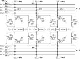
도 2는 본 발명의 여러 실시형태에 따라 데이터 시프팅을 수행하도록 구성된 메모리 어레이(230)의 일부의 도식적 선도를 예시한다. 어레이(230)는 소정 수의 액세스 라인(204-0(WL0), 204-1(WL1), 204-2(WL2), 204-3(WL3)) 및 소정 수의 감지 라인(205-0(D0), 205-1(D1), 205-2(D2))을 포함하는 제1 부분(예를 들어, 서브-어레이)를 포함한다. 또한, 어레이(230)는 소정 수의 액세스 라인(244-0(WL0), 244-1(WL1), 244-2(WL2), 244-3(WL3)), 및 각각 감지 라인(205-0, 205-1, 205-2)에 대한 상보적 감지 라인으로서 역할하는 소정 수의 감지 라인(265-0(D0_), 265-1(D1_), 265-2(D2_))을 포함하는 제2 부분을 포함한다. 그와 같이, 어레이(230)의 셀(201)은 액세스 라인(예를 들어, 워드 라인)에 의해 결합된 행 및 감지 라인(예를 들어, 디지트 라인)에 의해 결합된 열로 배열되며, 셀(201)의 각각의 열은 한 쌍의 상보적 감지 라인과 연관된다. 실시형태는 도 2에 도시된 소정 수의 열로 한정되지는 않는다.2 illustrates a schematic diagram of a portion of a
어레이(230)는, 예를 들어, 각각 액세스 디바이스(202) 및 저장 부재(예를 들어, 도 4에 도시된 바와 같이, 트랜지스터(402) 및 커패시터(403))로 이루어진 1T1C(일 트랜지스터 일 커패시터) 메모리 셀의 DRAM 어레이일 수 있다. 여러 실시형태에 있어서, 메모리 셀(201)은 파괴적 판독 메모리 셀이다(예를 들어, 셀에 저장된 데이터를 판독하는 것은 셀에 원래 저장된 데이터가 판독된 후에 리프레시되도록 데이터를 파괴한다).The
어레이(230)는 본 발명의 여러 실시형태에 따라 감지 회로에 결합된다. 이러한 예에 있어서, 각각의 쌍의 상보적 감지 라인은 (일반적으로는 (206)으로서 참조되는) 감지 증폭기 및 (일반적으로는 (231)로서 참조되는) 누산기를 포함하는 감지 회로에 결합된다. 예를 들면, 감지 라인(205-0/265-0)은 감지 증폭기(206-0(SA0)) 및 대응하는 누산기(231-0(ACCUM0))에 결합되고, 감지 라인(205-1/265-1)은 감지 증폭기(206-1(SA1)) 및 대응하는 누산기(231-1(ACCUM1))에 결합되고, 감지 라인(205-2/265-2)은 감지 증폭기(206-2(SA2)) 및 대응하는 누산기(231-2(ACCUM2))에 결합된다. 일례의 감지 증폭기는 도 5와 연관하여 설명되고, 일례의 누산기는 도 4와 연관하여 설명된다. 도 2에는 오픈 디지트 라인 아키텍처가 예시되기는 하지만, 실시형태는 그렇게 한정되지는 않는다. 예를 들면, 어레이(230)는, 다른 디지트 라인 아키텍처 중에서도, 도 4에 도시된 것과 같은 폴디드 디지트 라인 아키텍처를 가질 수 있다.The
감지 증폭기(206)는 감지(예를 들어, 판독) 연산을 통하여 선택된 셀에 저장된 데이터(예를 들어, 논리 데이터 값)를 결정하도록 동작될 수 있다. 누산기(231)는 여기에서 설명되는 실시형태에 따른 데이터 시프팅과 연관하여 메모리 셀로부터 판독된 데이터를 (예를 들어, 일시적으로) 저장하도록 동작될 수 있다. 아래에서 더 설명되는 바와 같이, 특정 디지트 라인에 결합된 감지 회로는 그 특정 디지트 라인에 결합된 메모리 셀로부터 또는 다른 디지트 라인(예를 들어, 인접 디지트 라인)에 결합된 메모리 셀로부터 데이터 값을 감지 및/또는 저장하도록 동작될 수 있다. 실시형태는 도 2에 도시된 예의 감지 회로로 한정되지는 않는다. 예를 들면, 여기에서 설명되는 여러 실시형태에 따른 감지 회로는 전류-모드 감지 증폭기 및/또는 싱글-엔디드 감지 증폭기(예를 들어, 하나의 감지 라인에 결합된 감지 증폭기)를 포함할 수 있다.The sense amplifier 206 may be operable to determine data (e.g., logical data values) stored in a selected cell through a sensing (e.g., read) operation. Accumulator 231 may be operable to store (e.g., temporarily) data read from the memory cell in association with data shifting in accordance with embodiments described herein. As will be described further below, the sensing circuit coupled to a particular digit line senses a data value from a memory cell coupled to that particular digit line or from a memory cell coupled to another digit line (e.g., adjacent digit line) And / or < / RTI > The embodiment is not limited to the sensing circuit of the example shown in Fig. For example, the sense circuit according to various embodiments described herein may include a current-mode sense amplifier and / or a single-ended sense amplifier (e.g., a sense amplifier coupled to one sense line).
본 발명의 여러 실시형태는 (예를 들어, 어레이(230)와 같은 어레이의 선택된 액세스 라인을 따라) 어레이에서 데이터를 시프팅하는 것과 연관하여 동작될 수 있는 소정 수의 격리 디바이스를 포함한다. 격리 디바이스는 특정 디지트 라인에 대응하는 감지 회로와 디지트 라인에 결합된 메모리 셀 사이에 위치할 수 있다. 예를 들면, 도 2에 도시된 예에 있어서, 디지트 라인(205-0, 205-1, 205-2)의 각각은 그들 각각의 감지 회로와 메모리 셀(201) 사이에 위치하는 3개의 격리 디바이스(251-1, 252-1, 253-1)를 포함한다. 유사하게, 상보적 디지트 라인(265-0, 265-1, 265-2)의 각각은 그들 각각의 감지 회로와 메모리 셀(201) 사이에 위치하는 3개의 격리 디바이스(251-2, 252-2, 253-2)를 포함한다.Various embodiments of the invention include a predetermined number of isolation devices that can be operated in association with shifting data in the array (e.g., along selected access lines of the array, such as array 230). The isolation device may be located between a sense circuit corresponding to a particular digit line and a memory cell coupled to the digit line. For example, in the example shown in FIG. 2, each of the digit lines 205-0, 205-1, 205-2 has three isolation devices (not shown) located between their respective sense circuits and the
예를 들면, 디지트 라인(205-1)에 관하여, 격리 디바이스(251-1)는 디지트 라인(205-1)에 결합된 메모리 셀과 감지 증폭기(206-1) 사이에 위치하고, 격리 디바이스(252-1)는 인접 디지트 라인(205-0)에 결합된 메모리 셀과 감지 증폭기(206-1) 사이에 위치하고, 격리 디바이스(253-1)는 인접 디지트 라인(205-2)에 결합된 메모리 셀과 감지 증폭기(206-1) 사이에 위치한다. 유사하게, 상보적 디지트 라인(265-1)에 관하여, 격리 디바이스(251-2)는 디지트 라인(265-1)에 결합된 메모리 셀과 감지 증폭기(206-1) 사이에 위치하고, 격리 디바이스(252-2)는 인접 디지트 라인(265-0)에 결합된 메모리 셀과 감지 증폭기(206-1) 사이에 위치하고, 격리 디바이스(253-2)는 인접 디지트 라인(265-2)에 결합된 메모리 셀과 감지 증폭기(206-1) 사이에 위치한다.For example, with respect to the digit line 205-1, the isolation device 251-1 is located between the memory cell coupled to the digit line 205-1 and the sense amplifier 206-1, and the isolation device 252 -1 is located between the memory cell coupled to the adjacent digit line 205-0 and the sense amplifier 206-1 and the isolation device 253-1 is located between the memory cell coupled to the adjacent digit line 205-0 and the sense amplifier 206-1, And the sense amplifier 206-1. Similarly, with respect to the complementary digit line 265-1, the isolation device 251-2 is located between the sense amplifier 206-1 and the memory cell coupled to the digit line 265-1, 252-2 are located between the memory cell coupled to the adjacent digit line 265-0 and the sense amplifier 206-1 and the isolation device 253-2 is located between the memory cell coupled to the adjacent digit line 265-0, Cell and the sense amplifier 206-1.
도 2에 도시된 예에 있어서, 격리 디바이스(251-1, 252-1, 253-1, 251-2, 252-2, 253-2)는 n-채널(Nch) 트랜지스터(예를 들어, 전계 효과 트랜지스터)이다; 그렇지만, 실시형태는 특정 유형의 트랜지스터 또는 다른 격리 디바이스로 한정되지는 않는다. 도 2에 도시된 예에 있어서 그리고 재차 디지트 라인(205-1)을 참조하면, 디지트 라인(205-1)에 대응하는 격리 디바이스(251-1)의 제1 단자(예를 들어, 소스/드레인), 디지트 라인(205-2)에 대응하는 격리 디바이스(252-1)의 제1 단자, 및 디지트 라인(205-0)에 대응하는 격리 디바이스(253-1)의 제1 단자는 서로에 그리고 디지트 라인(205-1)에 결합된다. 디지트 라인(205-2)에 대응하는 격리 디바이스(252-1)의 제2 단자는 감지 증폭기(206-2)에 결합되고, 디지트 라인(205-0)에 대응하는 격리 디바이스(253-1)의 제2 단자는 감지 증폭기(206-0)에 결합된다. 또한, 디지트 라인(205-1)에 대응하는 격리 디바이스(251-1)의 제2 단자, 디지트 라인(205-1)에 대응하는 격리 디바이스(252-1)의 제1 단자, 및 디지트 라인(205-1)에 대응하는 격리 디바이스(253-1)의 제1 단자는 서로에 그리고 감지 증폭기(206-1)에 결합된다.In the example shown in FIG. 2, isolation devices 251-1, 252-1, 253-1, 251-2, 252-2, and 253-2 are n-channel (Nch) Effect transistors); However, embodiments are not limited to any particular type of transistor or other isolation device. In the example shown in FIG. 2 and again referring to the digit line 205-1, the first terminal (e.g., source / drain) of the isolation device 251-1 corresponding to the digit line 205-1 The first terminal of the isolation device 252-1 corresponding to the digit line 205-2 and the first terminal of the isolation device 253-1 corresponding to the digit line 205-0 are connected to each other And is coupled to the digit line 205-1. The second terminal of the isolation device 252-1 corresponding to the digit line 205-2 is coupled to the sense amplifier 206-2 and the isolation device 253-1 corresponding to the digit line 205-0, Is coupled to the sense amplifier 206-0. The second terminal of the isolation device 251-1 corresponding to the digit line 205-1, the first terminal of the isolation device 252-1 corresponding to the digit line 205-1, And the first terminals of the isolation device 253-1 corresponding to the sense amplifiers 205-1 and 205-1 are coupled to each other and to the sense amplifier 206-1.
여러 실시형태에 있어서, 격리 디바이스(251-1, 252-1, 253-1, 251-2, 252-2, 253-2)는, 특정 피처 크기(예를 들어, 4F2, 6F2 등)에 순응할 수 있는, 어레이(230)의 감지 회로(예를 들어, 감지 증폭기(206) 및/또는 누산기(231)) 및/또는 메모리 셀(201)에 따른 피치로 형성될 수 있다. 격리 디바이스(251-1, 252-1, 253-1, 251-2, 252-2, 253-2)는 감지 증폭기(206)들 사이의 갭에 형성될 수 있어서, 이전의 접근법에 비해, 그러한 디바이스에 필요한 공간량을 감축하고 그리고/또는 다른 회로에 이용가능한 공간량을 증가시킬 수 있다. 그와 같이, 여기에서 설명되는 실시형태에 따라 데이터를 시프팅하기 위한 방법 및 장치는 이전의 접근법에 비해 이점을 갖는다.In some embodiments, isolation devices 251-1, 252-1, 253-1, 251-2, 252-2, and 253-2 may be configured to detect certain feature sizes (e.g., 4F2 , 6F2 , (E.g., the sense amplifier 206 and / or the accumulator 231) and / or the
동작에 있어서, 신호는 (예를 들어, 어레이(230)의 선택된 액세스 라인을 따라) 어레이 내에서 데이터를 시프팅하기 위해 격리 디바이스(251-1, 252-1, 253-1, 251-2, 252-2, 253-2)의 게이트에 (예를 들어, 도 1에 도시된 시프트 컨트롤러(170)를 통하여) 선택적으로 제공될 수 있다. 도 2에 도시된 예에 있어서, 격리 디바이스(251-1, 251-2)는 신호(241)(NORM)를 통하여 가능/불능으로 되고, 격리 디바이스(252-1, 252-1)는 신호(242)(ShftL)를 통하여 가능/불능으로 되고, 격리 디바이스(253-1, 253-2)는 신호(243)(ShftR)를 통하여 가능/불능으로 된다.In operation, the signals may be transmitted to the isolation devices 251-1, 252-1, 253-1, 251-2, 251-2, 252-2, and 253-2 (for example, through the
데이터는 여러 실시형태에 따라 (예를 들어, 선택된 액세스 라인을 따라) 우측으로 또는 좌측으로 시프팅될 수 있다. 예를 들어, 메모리 셀(201-1)에 저장된 데이터 값을 선택된 액세스 라인(204-1)을 따라 우측으로(예를 들어, 메모리 셀(201-2)로) 시프팅하기 위한 연산은 디지트 라인(205-1)에 대응하는 격리 디바이스(251-1)를 가능으로 하는(예를 들어, "NORM" 제어 신호(241)를 통하여 턴 온 하는) 한편 격리 디바이스(252-1, 253-1)를 ("ShftR" 및 "ShftL" 제어 신호를 통하여) 불능으로 하는 것을 포함할 수 있다. 격리 디바이스(251-1)가 가능으로 되면, 감지(예를 들어, 판독) 연산은 (예를 들어, 선택된 액세스 라인(204-1) 및 감지 증폭기(206-1)를 활성화함으로써) 메모리 셀(201-1)에 저장된 데이터 값을 결정하도록 수행될 수 있다. 감지된 데이터 값은 누산기(231-1)에 저장될 수 있다. 감지된 데이터 값은 그 후 디지트 라인(205-1)에 대응하는 격리 디바이스(253-1)를 (예를 들어, "ShftR" 제어 신호(243)를 통하여) 가능으로 하고 선택된 액세스 라인(204-1)을 활성화함으로써 셀(201-2)로 시프팅될 수 있다. 그와 같이, 격리 디바이스(253-1)가 가능으로 되어 있는 동안 액세스 라인(204-1)을 활성화하는 것은 누산기(231-1)에 저장된 데이터 값을 메모리 셀(201-2)에 기록한다. 그래서, 셀(201-1)에 저장된 데이터 값은 감지 라인 어드레스 액세스를 통하여 그리고 또는 I/O 라인을 통하여 어레이 밖으로 데이터를 전송함이 없이(예를 들어, 데이터가 로컬 I/O 라인을 통하여 어레이 및 감지 회로로부터 외부의 회로에 전송되도록 열 디코드 신호를 파이어링함이 없이) 셀(201-2)로 시프팅된다. 또한, 디지트 라인(205-1)에 대응하는 감지 회로에 의해 감지되는 셀(201-1)로부터의 데이터 값은 디지트 라인(205-2)에 대응하는 감지 회로에 전송되는 것 및/또는 그에 의해 감지되는 것 없이 셀(201-2)에 전송됨을 주목한다. 그와 같이, 데이터 값은 단일(예를 들어, 단 하나의) 감지 연산의 실행을 통하여 시프팅될 수 있다.The data may be shifted to the right or to the left according to various embodiments (e.g., along the selected access line). For example, an operation for shifting the data value stored in memory cell 201-1 to the right along the selected access line 204-1 (e.g., to memory cell 201-2) (For example, turning on via the "NORM" control signal 241) while enabling the isolation device 251-1 corresponding to the isolation device 251-1, while isolating devices 252-1, (Via the "ShftR" and "ShftL" control signals). (E.g., by activating the selected access line 204-1 and sense amplifier 206-1), the sensing (e.g., read) 201-1). The sensed data value may be stored in the accumulator 231-1. The sensed data value then enables the isolation device 253-1 (e.g., via the "ShftR" control signal 243) corresponding to the digit line 205-1 and the selected access line 204- 1) to the cell 201-2. As such, activating the access line 204-1 while the isolation device 253-1 is enabled records the data value stored in the accumulator 231-1 in the memory cell 201-2. Thus, the data values stored in the cell 201-1 can be transferred to the array 201-1 without transmitting data out of the array through the sense line address access and / or through the I / O line (e.g., And firing the column decode signal to be transferred from the sense circuitry to the external circuitry). Further, the data value from the cell 201-1 sensed by the sense circuit corresponding to the digit line 205-1 may be transmitted to the sense circuit corresponding to the digit line 205-2 and / Is transmitted to the cell 201-2 without being sensed. As such, the data value may be shifted through execution of a single (e.g., only one) sensing operation.
유사한 방식으로, 메모리 셀(201-1)에 저장된 데이터 값을 선택된 액세스 라인(204-1)을 따라 좌측으로(예를 들어, 메모리 셀(201-0)로) 시프팅하기 위한 연산은 디지트 라인(205-1)에 대응하는 격리 디바이스(251-1)를 가능으로 하는(예를 들어, "NORM" 제어 신호(241)를 통하여 턴 온 하는) 한편 격리 디바이스(252-1, 253-1)를 ("ShftR" 및 "ShftL" 제어 신호를 통하여) 불능으로 하는 것을 포함할 수 있다. 격리 디바이스(251-1)가 가능으로 되면, 감지(예를 들어, 판독) 연산은 (예를 들어, 선택된 액세스 라인(204-1) 및 감지 증폭기(206-1)를 활성화함으로써) 메모리 셀(201-1)에 저장된 데이터 값을 결정하도록 수행될 수 있다. 감지된 데이터 값은 (예를 들어, "ShftL" 제어 신호(242)를 통하여) 디지트 라인(205-1)에 대응하는 격리 디바이스(252-1)를 가능으로(예를 들어, 턴 온) 하고 선택된 액세스 라인(204-1)을 활성화함으로써 셀(201-0)로 시프팅될 수 있다. 그와 같이, 격리 디바이스(252-1)가 가능으로 되어 있는 동안 액세스 라인(204-1)을 활성화하는 것은 누산기(231-1)에 저장된 데이터 값을 메모리 셀(201-0)에 기록한다.In an analogous manner, the operation for shifting the data value stored in memory cell 201-1 to the left (e.g., to memory cell 201-0) along the selected access line 204-1 is performed by a digit line (For example, turning on via the "NORM" control signal 241) while enabling the isolation device 251-1 corresponding to the isolation device 251-1, while isolating devices 252-1, (Via the "ShftR" and "ShftL" control signals). (E.g., by activating the selected access line 204-1 and sense amplifier 206-1), the sensing (e.g., read) 201-1). The sensed data value enables (e. G., Turns on) the isolation device 252-1 corresponding to the digit line 205-1 (e.g., via the "ShftL" control signal 242) May be shifted to cell 201-0 by activating the selected access line 204-1. As such, activating the access line 204-1 while the isolation device 252-1 is enabled records the data value stored in the accumulator 231-1 in the memory cell 201-0.
위의 예는 단일 메모리 셀(예를 들어, 201-1)로부터 데이터를 시프팅하는 것에 초점을 맞추고는 있지만, 격리 디바이스(251-1, 252-1, 253-1 그리고 251-2, 252-2, 253-2)는 동시에 다수의 셀로부터 데이터를 시프팅하도록 동작될 수 있다. 예를 들면, 선택된 액세스 라인에 결합된 셀 전부로부터의 데이터(예를 들어, 데이터의 페이지)는 (예를 들어, 격리 디바이스(253-1/253-2)를 가능으로 하는 것을 통하여) 우측으로 또는 (예를 들어, 격리 디바이스(252-1/252-2)를 가능으로 하는 것을 통하여) 좌측으로 시프팅될 수 있다. 또한, 디지트 라인(265-0, 265-1, 265-2)에 결합된 셀에 저장된 데이터는 위에서 설명된 바와 유사한 방식으로 액세스 라인(244-0 내지 244-3)을 따라 시프팅될 수 있다. 도 2에서 예시되지는 않지만, 여러 실시형태에 있어서, 격리 디바이스는 데이터가 비-인접 메모리 셀로 시프팅될 수 있도록 비-인접 디지트 라인들 사이에 결합될 수 있다. 예를 들면, 메모리 셀(201-0)에 저장된 데이터 값은 메모리 셀(201-2)에 직접 전송될 수 있다. 더욱, 여러 실시형태에 있어서, 특정 메모리 셀(예를 들어, 201-0)로부터의 데이터는 하나보다 많은 메모리 셀에 전송될 수 있다.While the above example focuses on shifting data from a single memory cell (e.g., 201-1), isolation devices 251-1, 252-1, 253-1 and 251-2, 252-2, 2, and 253-2 may be operated to simultaneously shift data from a plurality of cells. For example, data (e.g., pages of data) from all of the cells coupled to the selected access line may be transmitted to the right (e.g., through enabling isolation device 253-1 / 253-2) Or may be shifted to the left (e.g., through enabling isolation device 252-1 / 252-2). Also, the data stored in the cells coupled to the digit lines 265-0, 265-1, 265-2 may be shifted along the access lines 244-0 through 244-3 in a manner similar to that described above . Although not illustrated in FIG. 2, in various embodiments, the isolation device can be coupled between non-adjacent digit lines so that data can be shifted to non-adjacent memory cells. For example, the data value stored in the memory cell 201-0 can be transferred directly to the memory cell 201-2. Moreover, in various embodiments, data from a particular memory cell (e.g., 201-0) may be transferred to more than one memory cell.
도 3은 본 발명의 여러 실시형태에 따라 데이터 시프팅을 수행하도록 구성된 메모리 어레이(330)의 일부의 도식적 선도를 예시한다. 어레이(330)는 소정 수의 액세스 라인(304-0(WL0), 304-1(WL1), 304-2(WL2), 304-3(WL3)) 및 소정 수의 감지 라인(305-0(D0), 305-1(D1), 305-2(D2))을 포함하는 제1 부분(예를 들어, 서브-어레이)를 포함한다. 또한, 어레이(330)는 소정 수의 액세스 라인(344-0(WL0), 344-1(WL1), 344-2(WL2), 344-3(WL3)), 및 각각 감지 라인(305-0, 305-1, 305-2)에 대한 상보적 감지 라인으로서 역할하는 소정 수의 감지 라인(365-0(D0_), 365-1(D1_), 365-2(D2_))을 포함하는 제2 부분을 포함한다. 그와 같이, 어레이(330)의 셀(301)은 액세스 라인(예를 들어, 워드 라인)에 의해 결합된 행 및 감지 라인(예를 들어, 디지트 라인)에 의해 결합된 열로 배열되며, 셀(301)의 각각의 열은 한 쌍의 상보적 감지 라인과 연관된다. 실시형태는 도 3에 도시된 소정 수의 열로 한정되지는 않는다.Figure 3 illustrates a schematic diagram of a portion of a
어레이(330)는, 예를 들어, 각각 액세스 디바이스 및 저장 부재(예를 들어, 도 4에 도시된 바와 같이, 트랜지스터(402) 및 커패시터(403))로 이루어진 1T1C(일 트랜지스터 일 커패시터) 메모리 셀의 DRAM 어레이일 수 있다. 여러 실시형태에 있어서, 메모리 셀(301)은 파괴적 판독 메모리 셀이다(예를 들어, 셀에 저장된 데이터를 판독하는 것은 셀에 원래 저장된 데이터가 판독된 후에 리프레시되도록 데이터를 파괴한다).The
어레이(330)는 본 발명의 여러 실시형태에 따라 감지 회로에 결합된다. 이러한 예에 있어서, 각각의 쌍의 상보적 감지 라인은 (일반적으로는 (306)으로서 참조되는) 감지 증폭기 및 (일반적으로는 (331)로서 참조되는) 누산기를 포함하는 감지 회로에 결합된다. 예를 들면, 감지 라인(305-0/365-0)은 감지 증폭기(306-0(SA0)) 및 대응하는 누산기(331-0(ACCUM0))에 결합되고, 감지 라인(305-1/365-1)은 감지 증폭기(306-1(SA1)) 및 대응하는 누산기(331-1(ACCUM1))에 결합되고, 감지 라인(305-3/365-2)은 감지 증폭기(306-2(SA2)) 및 대응하는 누산기(331-2(ACCUM2))에 결합된다. 일례의 감지 증폭기는 도 5와 연관하여 설명되고, 일례의 누산기는 도 4와 연관하여 설명된다.The
감지 증폭기(306)는 감지(예를 들어, 판독) 연산을 통하여 선택된 셀에 저장된 데이터(예를 들어, 논리 데이터 값)를 결정하도록 동작될 수 있다. 누산기(331)는 여기에서 설명되는 실시형태에 따른 데이터 시프팅과 연관하여 메모리 셀로부터 판독된 데이터를 (예를 들어, 일시적으로) 저장하도록 동작될 수 있다. 아래에서 더 설명되는 바와 같이, 특정 디지트 라인에 결합된 감지 회로는 그 특정 디지트 라인에 결합된 메모리 셀로부터 또는 다른 디지트 라인(예를 들어, 인접 디지트 라인)에 결합된 메모리 셀로부터 데이터 값을 감지 및/또는 저장하도록 동작될 수 있다. 실시형태는 도 3에 도시된 예의 감지 회로로 한정되지는 않는다.The sense amplifier 306 may be operable to determine data (e.g., logical data values) stored in a selected cell through a sensing (e.g., read) operation. The accumulator 331 may be operable to store (e.g., temporarily) the data read from the memory cell in association with the data shifting in accordance with the embodiments described herein. As will be described further below, the sensing circuit coupled to a particular digit line senses a data value from a memory cell coupled to that particular digit line or from a memory cell coupled to another digit line (e.g., adjacent digit line) And / or < / RTI > The embodiment is not limited to the sensing circuit of the example shown in Fig.
어레이(330)는 특정 디지트 라인에 대응하는 감지 회로와 디지트 라인에 결합된 메모리 셀 사이에 위치하는 격리 디바이스를 포함한다. 예를 들면, 도 3에 도시된 예에 있어서, 디지트 라인(305-0, 305-1, 305-2)의 각각은 그들 각각의 감지 회로와 대응하는 메모리 셀(301) 사이에 위치하는 제1 격리 디바이스(351-1), 및 그들 각각의 메모리 셀(301)과 인접 디지트 라인에 대응하는 감지 회로 사이에 위치하는 제2 격리 디바이스(355-1)를 포함한다. 예를 들면, 디지트 라인(305-0)에 대응하는 격리 디바이스(355-1)는 디지트 라인(305-0)의 메모리 셀과 디지트 라인(305-1)에 대응하는 감지 회로 사이에 위치하고, 디지트 라인(305-1)에 대응하는 격리 디바이스(355-1)는 디지트 라인(305-1)의 메모리 셀과 디지트 라인(305-2)에 대응하는 감지 회로 사이에 위치하고, 도 3에서 도시되지는 않지만, 디지트 라인(305-2)에 대응하는 격리 디바이스(355-1)는 디지트 라인(305-2)의 메모리 셀과 다음 인접 디지트 라인에 대응하는 감지 회로 사이에 위치한다. 유사하게, 상보적 디지트 라인(365-0, 365-1, 365-2)의 각각은 그들 각각의 감지 회로와 대응하는 메모리 셀(301) 사이에 위치하는 제1 격리 디바이스(351-1), 및 그들 각각의 메모리 셀(301)과 인접 디지트 라인에 대응하는 감지 회로 사이에 위치하는 제2 격리 디바이스(355-1)를 포함한다.The
일례로서, 디지트 라인(305-1)에 관하여, 격리 디바이스(351-1)는 디지트 라인(305-1)에 결합된 메모리 셀과 감지 증폭기(306-1) 사이에 위치하고, 격리 디바이스(355-1)는 인접 디지트 라인(305-0)에 결합된 메모리 셀과 감지 증폭기(306-1) 사이에 위치한다. 유사하게, 상보적 디지트 라인(365-1)에 관하여, 격리 디바이스(351-2)는 디지트 라인(365-1)에 결합된 메모리 셀과 감지 증폭기(306-1) 사이에 위치하고, 격리 디바이스(355-2)는 인접 디지트 라인(365-0)에 결합된 메모리 셀과 감지 증폭기(306-1) 사이에 위치한다.As an example, with respect to the digit line 305-1, the isolation device 351-1 is located between the memory cell coupled to the digit line 305-1 and the sense amplifier 306-1, and the isolation device 355- 1 is located between the sense amplifier 306-1 and the memory cell coupled to the adjacent digit line 305-0. Similarly, with respect to the complementary digit line 365-1, the isolation device 351-2 is located between the sense amplifier 306-1 and the memory cell coupled to the digit line 365-1, 355-2 are located between the sense amplifier 306-1 and the memory cell coupled to the adjacent digit line 365-0.
도 3에 도시된 예에 있어서, 격리 디바이스(351-1, 355-1, 351-2, 355-2)는 n-채널(Nch) 트랜지스터(예를 들어, 전계 효과 트랜지스터)이다; 그렇지만, 실시형태는 특정 유형의 트랜지스터 또는 다른 격리 디바이스로 한정되지는 않는다. 도 3에 도시된 예에 있어서 그리고 재차 디지트 라인(305-1)을 참조하면, 디지트 라인(305-1)에 대응하는 격리 디바이스(351-1)의 제1 단자(예를 들어, 소스/드레인) 및 디지트 라인(305-1)에 대응하는 격리 디바이스(355-1)의 제1 단자는 서로에 그리고 감지 증폭기(306-1)에 결합된다. 디지트 라인(305-1)에 대응하는 격리 디바이스(355-1)의 제2 단자 및 디지트 라인(305-0)에 대응하는 격리 디바이스(351-1)의 제1 단자는 서로에 그리고 디지트 라인(305-0)에 결합되며, 디지트 라인(305-0)에 대응하는 격리 디바이스(351-1)의 제2 단자는 감지 증폭기(306-0)에 결합된다. 디지트 라인(305-1)에 대응하는 격리 디바이스(351-1)의 제2 단자 및 디지트 라인(305-2)에 대응하는 격리 디바이스(355-1)의 제1 단자는 서로에 그리고 디지트 라인(305-1)에 결합된다. 또한, 디지트 라인(305-2)에 대응하는 격리 디바이스(355-1)의 제2 단자 및 디지트 라인(305-2)에 대응하는 격리 디바이스(351-1)의 제1 단자는 서로에 그리고 감지 증폭기(306-2)에 결합되며, 디지트 라인(305-2)에 대응하는 격리 디바이스(351-1)의 제2 단자는 다음 인접 디지트 라인(도시되지 않음)에 대응하는 격리 디바이스(355-1)에 그리고 디지트 라인(305-2)에 결합된다.In the example shown in FIG. 3, isolation devices 351-1, 355-1, 351-2, and 355-2 are n-channel (Nch) transistors (e.g., field effect transistors); However, embodiments are not limited to any particular type of transistor or other isolation device. 3, and again referring to the digit line 305-1, the first terminal (e.g., source / drain) of the isolation device 351-1 corresponding to the digit line 305-1 And the first terminal of the isolation device 355-1 corresponding to the digit line 305-1 are coupled to each other and to the sense amplifier 306-1. The second terminal of the isolation device 355-1 corresponding to the digit line 305-1 and the first terminal of the isolation device 351-1 corresponding to the digit line 305-0 are connected to each other and to the digit line And the second terminal of the isolation device 351-1 corresponding to the digit line 305-0 is coupled to the sense amplifier 306-0. The second terminal of the isolation device 351-1 corresponding to the digit line 305-1 and the first terminal of the isolation device 355-1 corresponding to the digit line 305-2 are connected to each other and to the digit line 305-1. The second terminal of the isolation device 355-1 corresponding to the digit line 305-2 and the first terminal of the isolation device 351-1 corresponding to the digit line 305-2 are connected to each other And the second terminal of the isolation device 351-1 corresponding to the digit line 305-2 is connected to the isolation device 355-1 corresponding to the next adjacent digit line (not shown) And to the digit line 305-2.
여러 실시형태에 있어서, 격리 디바이스(351-1, 355-1, 351-2, 355-2)는, 특정 피처 크기(예를 들어, 4F2, 6F2 등)에 순응할 수 있는, 어레이(330)의 감지 회로(예를 들어, 감지 증폭기(306) 및/또는 누산기(331)) 및/또는 메모리 셀(301)에 따른 피치로 형성될 수 있다.In various embodiments, isolation devices 351-1, 355-1, 351-2, and 355-2 may be array (s) that can be compliant with a particular feature size (e.g., 4F2 , 6F2 , (E.g., the sense amplifier 306 and / or the accumulator 331) and / or the
동작에 있어서, 신호는 (예를 들어, 어레이(330)의 선택된 액세스 라인을 따라) 어레이 내에서 데이터를 시프팅하기 위해 격리 디바이스(351-1, 355-1, 351-2, 355-2)의 게이트에 (예를 들어, 도 1에 도시된 시프트 컨트롤러(170)를 통하여) 선택적으로 제공될 수 있다. 도 3에 도시된 예에 있어서, 격리 디바이스(351-1, 351-2)는 신호(341)(NORM)를 통하여 가능/불능으로 되고, 격리 디바이스(355-1, 355-1)는 신호(345)(Shft)를 통하여 가능/불능으로 된다.In operation, the signals may be provided to isolation devices 351-1, 355-1, 351-2, and 355-2 to shift data within the array (e.g., along the selected access line of array 330) (For example, via the
데이터는 여러 실시형태에 따라 (예를 들어, 선택된 액세스 라인을 따라) 우측으로 또는 좌측으로 시프팅될 수 있다. 예를 들어, 메모리 셀(301-1)에 저장된 데이터 값을 선택된 액세스 라인(304-1)을 따라 좌측으로(예를 들어, 메모리 셀(301-0)로) 시프팅하기 위한 연산은 디지트 라인(305-1)에 대응하는 격리 디바이스(351-1)를 (예를 들어, "NORM" 제어 신호(341)를 통하여) 가능으로 하는 한편 격리 디바이스(355-1)를 ("Shft" 제어 신호를 통하여) 불능으로 하는 것을 포함할 수 있다. 격리 디바이스(351-1)가 가능으로 되면, 감지(예를 들어, 판독) 연산은 (예를 들어, 선택된 액세스 라인(304-1) 및 감지 증폭기(306-1)를 활성화함으로써) 메모리 셀(301-1)에 저장된 데이터 값을 결정하도록 수행될 수 있다. 감지된 데이터 값은 누산기(331-1)에 저장될 수 있다. 감지된 데이터 값은 그 후 디지트 라인(305-1)에 대응하는 격리 디바이스(355-1)를 (예를 들어, "Shft" 제어 신호(345)를 통하여) 가능으로 하고 선택된 액세스 라인(304-1)을 활성화함으로써 셀(301-0)로 시프팅될 수 있다. 그와 같이, 격리 디바이스(355-1)가 가능으로 되어 있는 동안 액세스 라인(304-1)을 활성화하는 것은 누산기(331-1)에 저장된 데이터 값을 메모리 셀(301-0)에 기록한다. 그래서, 셀(301-1)에 저장된 데이터 값은 감지 라인 어드레스 액세스를 통하여 그리고 또는 I/O 라인을 통하여 어레이 밖으로 데이터를 전송함이 없이(예를 들어, 데이터가 로컬 I/O 라인을 통하여 어레이 및 감지 회로로부터 외부의 회로에 전송되도록 열 디코드 신호를 파이어링함이 없이) 셀(301-0)로 시프팅된다. 또한, 디지트 라인(305-1)에 대응하는 감지 회로에 의해 감지되는 셀(301-1)로부터의 데이터 값은 디지트 라인(305-0)에 대응하는 감지 회로에 전송되는 것 및/또는 그에 의해 감지되는 것 없이 셀(301-0)에 전송됨을 주목한다. 그와 같이, 데이터 값은 단일(예를 들어, 단 하나의) 감지 연산의 실행을 통하여 (예를 들어, 좌측으로) 시프팅될 수 있다.The data may be shifted to the right or to the left according to various embodiments (e.g., along the selected access line). For example, an operation for shifting the data value stored in the memory cell 301-1 to the left (e.g., to the memory cell 301-0) along the selected access line 304-1 may be performed by a digit line Quot; control signal 341) while allowing the isolation device 351-1 (corresponding to the " Shft " control signal 351-1) ≪ / RTI > (E. G., By activating the selected access line 304-1 and sense amplifier 306-1), the sensing (e. G., Reading) 301-1). ≪ / RTI > The sensed data value may be stored in the accumulator 331-1. The sensed data value then enables the isolation device 355-1 corresponding to the digit line 305-1 (e.g., via the "Shft" control signal 345) and the selected access line 304- 1) to the cell 301-0. As such, activating the access line 304-1 while the isolation device 355-1 is enabled records the data value stored in the accumulator 331-1 in the memory cell 301-0. Thus, the data values stored in the cell 301-1 may be transferred to the array 301-1 without transmitting data out of the array through the sense line address access and / or through the I / O line (e.g., And firing the column decode signal to be transferred from the sense circuit to the external circuit). Further, the data value from the cell 301-1 sensed by the sense circuit corresponding to the digit line 305-1 may be transmitted to the sense circuit corresponding to the digit line 305-0 and / Is transmitted to the cell 301-0 without being sensed. As such, the data value may be shifted (e.g., to the left) through the execution of a single (e.g., only one) sensing operation.
메모리 셀(301-1)에 저장된 데이터 값을 선택된 액세스 라인(304-1)을 따라 우측으로(예를 들어, 메모리 셀(301-2)로) 시프팅하기 위한 연산은 디지트 라인(305-2)에 대응하는 격리 디바이스(355-1)를 (예를 들어, "Shft" 제어 신호(345)를 통하여) 가능으로 하고, 디지트 라인(305-1)에 대응하는 격리 디바이스(351-1)를 ("NORM" 제어 신호(341)를 통하여) 불능으로 하고, (예를 들어, 선택된 액세스 라인(304-1) 및 감지 증폭기(306-2)를 활성화함으로써) 메모리 셀(301-1)에 저장된 데이터 값을 감지(예를 들어, 판독)하는 것을 포함할 수 있다. 감지 증폭기(306-2)에 의해 감지된 데이터 값은 누산기(331-2)에 저장될 수 있다. 그와 같이, 셀(301-1)에 저장된 데이터 값은 디지트 라인(305-2)에 대응하는 감지 회로(예를 들어, 누산기(331-2))로 시프팅된다. 감지된 데이터 값은 그 후 디지트 라인(305-2)에 대응하는 격리 디바이스(351-1)를 (예를 들어, "NORM" 제어 신호(341)를 통하여) 가능으로 하고 선택된 액세스 라인(304-1)을 활성화함으로써 누산기(331-2)로부터 메모리 셀(301-2)에 기록될 수 있다. 즉, 디지트 라인(305-2)에 대응하는 격리 디바이스(351-1)가 가능으로 되어 있는 동안 액세스 라인(304-1)을 활성화하는 것은 누산기(331-2)에 저장된 데이터 값을 메모리 셀(301-2)에 기록한다.The operation for shifting the data value stored in the memory cell 301-1 to the right along the selected access line 304-1 (e.g., to the memory cell 301-2) (For example, via the "Shft" control signal 345) corresponding to the digit line 305-1 and the isolation device 351-1 corresponding to the digit line 305-1 (Via the "NORM" control signal 341) and stored in the memory cell 301-1 (e.g., by activating the selected access line 304-1 and sense amplifier 306-2) (E. G., Reading) the data value. The data value sensed by the sense amplifier 306-2 may be stored in the accumulator 331-2. As such, the data value stored in the cell 301-1 is shifted to the sense circuit (e.g., the accumulator 331-2) corresponding to the digit line 305-2. The sensed data value then makes the isolation device 351-1 (e.g., via the "NORM" control signal 341) corresponding to the digit line 305-2 enabled and the selected access line 304- 1) to the memory cell 301-2 from the accumulator 331-2. That is, activating the access line 304-1 while the isolation device 351-1 corresponding to the digit line 305-2 is enabled will cause the data value stored in the accumulator 331-2 to be stored in the memory cell 301-2.
위의 예는 단일 메모리 셀(예를 들어, 301-1)로부터 데이터를 시프팅하는 것에 초점을 맞추고는 있지만, 격리 디바이스(351-1, 355-1, 351-2, 355-2)는 동시에 다수의 셀로부터 데이터를 시프팅하도록 동작될 수 있다. 예를 들면, 선택된 액세스 라인에 결합된 셀 전부로부터의 데이터(예를 들어, 데이터의 페이지)는 특정 디지트 라인의 메모리 셀에 저장된 데이터 값을 판독하여 거기에 대응하는 각각의 감지 회로에 넣도록 격리 디바이스(351-1)를 가능으로 하고 그리고 그 후 격리 디바이스(355-1)가 가능으로 되어 있는 동안 선택된 액세스 라인을 활성화함으로써 각각의 감지 회로로부터의 데이터 값을 인접 메모리 셀에 기록하도록 격리 디바이스(355-1)를 가능으로 하는 것에 의해 좌측으로 시프팅될 수 있다. 데이터의 페이지는, 예를 들어, 격리 디바이스(355-1)를 가능으로 하고 그리고 특정 디지트 라인의 메모리 셀에 저장된 데이터 값을 판독하여 특정 디지트 라인에 인접하는 디지트 라인에 대응하는 감지 회로에 넣음으로써 우측으로 시프팅될 수 있다. 그 후 격리 디바이스(351-1)는 감지 회로로부터의 데이터 값을 거기에 대응하는 메모리 셀에 기록하도록 가능으로 될 수 있다. 디지트 라인(365-0, 365-1, 365-2)에 결합된 셀에 저장된 데이터는 위에서 설명된 바와 유사한 방식으로 액세스 라인(344-0 내지 344-3)을 따라 시프팅될 수 있다.While the example above focuses on shifting data from a single memory cell (e.g., 301-1), isolation devices 351-1, 355-1, 351-2, and 355-2 And may be operable to shift data from multiple cells. For example, data (e.g., pages of data) from all of the cells coupled to a selected access line may be read by a data value stored in a memory cell of a particular digit line, To enable the device 351-1 and then to activate the selected access line while the isolation device 355-1 is enabled, to write the data value from each sensing circuit to the adjacent memory cell 355-1). ≪ / RTI > A page of data may be generated by enabling isolation device 355-1, for example, and by reading the data value stored in the memory cell of a particular digit line and putting it into the sense circuit corresponding to the digit line adjacent to the particular digit line Can be shifted to the right. The isolation device 351-1 may then be enabled to write the data value from the sense circuit to the corresponding memory cell. Data stored in the cells coupled to the digit lines 365-0, 365-1, 365-2 may be shifted along the access lines 344-0 through 344-3 in a manner similar to that described above.
도 4는 본 발명의 여러 실시형태에 따라 데이터 시프팅을 수행하도록 구성된 메모리 어레이(430)의 일부의 도식적 선도를 예시한다. 이러한 예에 있어서, 메모리 어레이(430)는 각각 액세스 디바이스(402)(예를 들어, 트랜지스터) 및 저장 부재(403)(예를 들어, 커패시터)로 이루어진 1T1C(일 트랜지스터 일 커패시터) 메모리 셀의 DRAM 어레이이다. 어레이(430)의 셀은 워드 라인(404-0(WL0), 404-1(WL1), 404-2(WL2), 404-3(WL3), ..., 404-N(WLN))에 의해 결합된 행 및 감지 라인(예를 들어, 디지트 라인)(405-1(D), 405-2(D_))에 의해 결합된 열로 배열된다. 이러한 예에 있어서, 셀의 각각의 열은 한 쌍의 상보적 감지 라인(405-1(D), 405-2(D_))과 연관된다. 도 4에는 메모리 셀의 단일 열만이 예시되어 있지만, 실시형태는 그렇게 한정되지는 않는다. 예를 들면, 특정 어레이는 감지 라인 및/또는 메모리 셀의 소정 수의 열을 가질 수 있다(예를 들어, 4,096, 8,192, 16,384 등). 특정 메모리 셀 트랜지스터(402)의 게이트는 그 대응하는 워드 라인(404-0, 404-1, 404-2, 404-3, ..., 404-N)에 결합되고, 제1 소스/드레인 영역은 그 대응하는 감지 라인(405-1)에 결합되고, 특정 메모리 셀 트랜지스터의 제2 소스/드레인 영역은 그 대응하는 커패시터(403)에 결합된다. 도 4에는 예시되지는 않지만, 감지 라인(405-2)도 소정 수의 메모리 셀에 결합될 수 있다.Figure 4 illustrates a schematic diagram of a portion of a
어레이(430)는 본 발명의 여러 실시형태에 따라 감지 회로에 결합된다. 이러한 예에 있어서, 감지 회로는 감지 증폭기(406) 및 누산기(431)를 포함한다. 감지 회로는 도 1에 도시된 감지 회로(150)일 수 있다. 감지 증폭기(406)는 메모리 셀의 특정 열에 대응하는 상보적 감지 라인(D/ D_)에 결합된다. 감지 증폭기(406)는 도 5와 연관하여 아래에서 설명되는 감지 증폭기(506)와 같은 감지 증폭기일 수 있다. 그와 같이, 감지 증폭기(406)는 선택된 셀에 저장된 데이터 값을 결정하도록 동작될 수 있다. 실시형태는 그 예의 감지 증폭기(406)로 한정되지는 않는다.The
도 4에 도시된 예는 디지트 라인(405-1)에 결합된 메모리 셀과 감지 증폭기(406) 사이에 위치하는 격리 회로(471-1) 및 상보적 감지 라인(405-2)에 결합된 메모리 셀(도시되지 않음)과 감지 증폭기(406) 사이에 위치하는 격리 회로(471-2)를 포함한다. 격리 회로(471-1 및/또는 471-2)는, 도 2 및 도 3과 연관하여 설명된 바와 같은 소정 수의 트랜지스터와 같은, 소정 수의 격리 디바이스를 포함할 수 있다.4 includes an isolation circuit 471-1 located between the memory cell coupled to the digit line 405-1 and the
도 4에 도시된 예에 있어서, 누산기(431)는, 특정 피처 크기(예를 들어, 4F2, 6F2 등)에 순응할 수 있는, 어레이(430)의 메모리 셀 및/또는 감지 증폭기(406)의 트랜지스터에 따른 피치로 형성된 소정 수의 트랜지스터를 포함한다. 회로(471-1, 471-2)의 격리 디바이스도 어레이(430)의 메모리 셀에 따른 피치로 형성될 수 있다. 누산기(431)는, 감지 증폭기(406) 및 격리 회로(471-1/471-2)와 함께, 여기에서 설명되는 실시형태에 따른 데이터 시프팅을 수행하도록 동작한다.4, the
도 4에 예시된 예에 있어서, 누산기(431)에 대응하는 회로는 감지 라인(D, D_)의 각각에 결합된 5개의 트랜지스터를 포함한다; 그렇지만, 실시형태는 이러한 예에 한정되지는 않는다. 트랜지스터(407-1, 407-2)는, 각각, 감지 라인(D, D_)에 결합된 제1 소스/드레인 영역, 및 교차 결합 래치에 결합된(예를 들어, 교차 결합 NMOS 트랜지스터(408-1, 408-2) 및 교차 결합 PMOS 트랜지스터(409-1, 409-2)와 같은 한 쌍의 교차 결합 트랜지스터의 게이트에 결합된) 제2 소스/드레인 영역을 갖는다. 트랜지스터(408-1, 408-2, 409-1, 409-2)를 포함하는 교차 결합 래치는 여기에서 설명되는 바와 같은 데이터 시프팅과 연관하여 데이터 값을 일시적으로 저장하도록 사용될 수 있다.In the example illustrated in FIG. 4, the circuit corresponding to the
트랜지스터(407-1, 407-2)는, 각각의 감지 라인(D, D_) 상의 전압 또는 전류를 트랜지스터(408-1, 408-2, 409-1, 409-2)를 포함하는 교차 결합 래치의 입력에 패스하기 위해 각각의 신호(411-1(Passd), 411-2(Passdb))를 통하여 가능으로 될 수 있는, 패스 트랜지스터라고 지칭될 수 있다. 이러한 예에 있어서, 트랜지스터(407-1)의 제2 소스/드레인 영역은 트랜지스터(408-1, 409-1)의 제1 소스/드레인 영역에는 물론 트랜지스터(408-2, 409-2)의 게이트에도 결합된다. 유사하게, 트랜지스터(407-2)의 제2 소스/드레인 영역은 트랜지스터(408-2, 409-2)의 제1 소스/드레인 영역에는 물론 트랜지스터(408-1, 409-1)의 게이트에도 결합된다.Transistors 407-1 and 407-2 may be configured to provide voltages or currents on respective sense lines D and D_ to cross-coupled latches 408-1, 408-2, 409-1 and 409-2, May be referred to as a pass transistor, which may be enabled through respective signals 411-1 (Passd), 411-2 (Passdb) to pass the input of the transistor 411-1. In this example, the second source / drain region of transistor 407-1 is connected to the first source / drain region of transistors 408-1 and 409-1 as well as to the gate of transistors 408-2 and 409-2 Lt; / RTI > Similarly, the second source / drain region of transistor 407-2 is coupled to the first source / drain region of transistors 408-2 and 409-2 as well as to the gates of transistors 408-1 and 409-1. do.
트랜지스터(408-1, 408-2)의 제2 소스/드레인 영역은 음성 제어 신호(412-1)(Accumb)에 공통으로 결합된다. 트랜지스터(409-1, 409-2)의 제2 소스/드레인 영역은 양성 제어 신호(412-2)(Accum)에 공통으로 결합된다. Accum 신호(412-2)는 전원 전압(예를 들어, VDD)일 수 있고, Accumb 신호는 참조 전압(예를 들어, 그라운드)일 수 있다. 신호(412-1, 412-2)를 가능으로 하는 것은 트랜지스터(408-1, 408-2, 409-1, 409-2)를 포함하는 교차 결합 래치를 활성화한다. 활성화된 감지 증폭기 쌍은 노드(417-1)가 Accum 신호 전압 및 Accumb 신호 전압 중 하나로(예를 들어, VDD 및 그라운드 중 하나로) 구동되고 노드(417-2)가 Accum 신호 전압 및 Accumb 신호 전압 중 다른 하나로 구동되도록 공통 노드(417-1)와 공통 노드(417-2) 간 차동 전압을 증폭하도록 동작한다.The second source / drain regions of the transistors 408-1 and 408-2 are commonly coupled to the voice control signal 412-1 (Accumb). The second source / drain regions of the transistors 409-1 and 409-2 are commonly coupled to the positive control signal 412-2 (Accum). Accum signal 412-2 may be a supply voltage (e.g., VDD), and the Accumb signal may be a reference voltage (e.g., ground). Enabling signals 412-1 and 412-2 activates a cross-coupled latch that includes transistors 408-1, 408-2, 409-1, and 409-2. The activated sense amplifier pair is activated when node 417-1 is driven to one of the Accum signal voltage and the Accumb signal voltage (e.g., to VDD and ground) and node 417-2 is driven to either Accum signal voltage and Accumb signal voltage And operates to amplify the differential voltage between the common node 417-1 and the common node 417-2 so as to be driven to the other.
이러한 예에 있어서, 누산기(431)는 또한 각각의 디지트 라인(D, D_)에 결합된 제1 소스/드레인 영역을 갖는 반전 트랜지스터(414-1, 414-2)를 포함한다. 트랜지스터(414-1, 414-2)의 제2 소스/드레인 영역은, 각각, 트랜지스터(416-1, 416-2)의 제1 소스/드레인 영역에 결합된다. 트랜지스터(414-1, 414-2)의 게이트는 신호(413)(InvD)에 결합된다. 트랜지스터(416-1)의 게이트는 트랜지스터(408-2)의 게이트, 트랜지스터(409-2)의 게이트 및 트랜지스터(408-1)의 제1 소스/드레인 영역도 결합되는 공통 노드(417-1)에 결합된다. 상보적 방식으로, 트랜지스터(416-2)의 게이트는 트랜지스터(408-1)의 게이트, 트랜지스터(409-1)의 게이트 및 트랜지스터(408-2)의 제1 소스/드레인 영역도 결합되는 공통 노드(417-2)에 결합된다. 그와 같이, 신호(InvD)를 가능으로 하는 것은 이차적 래치에 저장된 데이터 값을 반전하는 역할을 하고 반전된 값을 감지 라인(405-1, 405-2) 상에 구동한다.In this example, the
도 4에 도시된 누산기(431)는, 예를 들어, 도 2 및 도 3과 연관하여 위에서 설명된 바와 같은 데이터 시프팅과 연관하여 데이터를 저장하도록 (예를 들어, Passd, Passdb, Accumb, Accum, 및 InvD 신호를 통하여) 동작될 수 있다. 예를 들면, 동작에 있어서, 메모리 셀에 저장된 데이터 값은 셀이 결합되는 액세스 라인을 활성화함으로써 감지될 수 있다. 선택된 액세스 라인의 활성화는 선택된 셀에 대응하는 액세스 트랜지스터(예를 들어, 402)를 가능으로 하여, 감지 라인(D, D_) 간 차동 전압 신호를 생성하는, 선택된 메모리 셀로의(예를 들어, 셀이 1T1C DRAM 셀이면 커패시터(403)로의) 감지 라인(D)의 결합을 초래한다. 감지 증폭기(406)는 (예를 들어, 도 5에 설명되는 신호(PSA, RNL_)와 같은 제어 신호의 인가를 통하여) 활성화하여, 논리 1에 대응하는 전압(예를 들어, VDD) 또는 논리 0에 대응하는 전압(예를 들어, 그라운드)이 감지 라인(D) 상에 있는 (그리고 다른 전압이 상보적 감지 라인(D_) 상에 있는) 결과를 초래하는 D와 D_ 간 차동 신호를 증폭하여, 감지된 데이터 값이 감지 증폭기(406)의 일차적 래치에 저장되게 한다.The
감지 증폭기(406)에 저장된 데이터 값은 (예를 들어, 각각, 제어 라인(411-1, 411-2)에 인가된 각각의 Passd 및 Passdb 제어 신호를 통하여) 패스 트랜지스터(407-1, 407-2)를 가능으로 함으로써 누산기에 저장될 수 있다. 제어 신호(411-1, 411-2)는 일괄하여 제어 신호(411)라고 지칭된다. 여기에서 사용될 때, Passd 및 Passdb와 같은 다양한 제어 신호는 신호가 인가되는 제어 라인을 가리킴으로써 참조표시될 수 있다. 예를 들면, Passd 신호는 제어 신호(411-1)라고 지칭될 수 있다. 패스 트랜지스터(407-1, 407-2)가 가능으로 되면, 제어 신호(Accumb, Accum)는 각각의 제어 라인(412-1, 412-2)을 통하여 활성화되어, 누산기(431)의 래치를 활성화한다. 그와 같이, 감지 증폭기(406)에 저장된 감지된 데이터 값은 누산기 래치에 전송(예를 들어, 복사)된다.The data values stored in
도 2 및 도 3과 연관하여 위에서 설명된 바와 같이, 감지 증폭기가 감지 연산 동안 결합되는 특정 메모리 셀은 격리 회로(471-1/471-2)의 어느 격리 디바이스가 가능으로 되는지에 의존할 수 있다. 예를 들면, 특정 디지트 라인에 대응하는 감지 증폭기는 도 3에 도시된 격리 디바이스(355-1)와 같은 격리 디바이스 또는 도 2에 도시된 격리 디바이스(252-1, 253-1)와 같은 격리 디바이스의 가능으로 함을 통하여 인접 디지트 라인의 메모리 셀에 결합될 수 있다.As described above in connection with FIGS. 2 and 3, the particular memory cell to which the sense amplifiers are coupled during the sensing operation may depend on which isolation device of the isolation circuit 471-1 / 471-2 is enabled . For example, a sense amplifier corresponding to a particular digit line may be connected to an isolation device such as isolation device 355-1 shown in FIG. 3 or isolation device 252-1, 253-1 shown in FIG. To the memory cell of the adjacent digit line.
도 5는 본 발명의 여러 실시형태에 따른 감지 회로의 일부의 도식적 선도를 예시한다. 이러한 예에 있어서, 감지 회로의 그 일부는 감지 증폭기(506)를 포함한다. 여러 실시형태에 있어서, 어레이(예를 들어, 어레이(130, 230, 330, 430))에서 메모리 셀의 각각의 열에 대해 하나의 감지 증폭기(506)가 제공된다. 감지 증폭기(506)는, 예를 들면, DRAM 어레이의 감지 증폭기일 수 있다. 감지 증폭기(506)는 각각 도 2, 도 3 및 도 4와 연관하여 위에서 설명된 감지 증폭기(206, 306, 406)와 같은 감지 증폭기일 수 있다.Figure 5 illustrates a schematic diagram of a portion of a sensing circuit in accordance with various embodiments of the present invention. In this example, a portion of the sensing circuit includes a
이러한 예에 있어서, 감지 증폭기(506)는 한 쌍의 상보적 감지 라인(505-1("D"), 505-2("D_"))과 연관된다. 그와 같이, 감지 증폭기(506)는 감지 라인(D, D_)을 통해 각각의 열에서 메모리 셀 전부에 결합된다.In this example,
감지 증폭기(506)는 음성 제어 신호(528(RNL_))에 결합된 그들 각각의 소스 및, 각각, 감지 라인(D, D_)에 결합된 그들 드레인을 갖는 한 쌍의 교차 결합 n-채널 트랜지스터(예를 들어, NMOS 트랜지스터)(527-1, 527-2)를 포함한다. 감지 증폭기(506)는 양성 제어 신호(531(PSA))에 결합된 그들 각각의 소스 및, 각각, 감지 라인(D, D_)에 결합된 그들 드레인을 갖는 한 쌍의 교차 결합 p-채널 트랜지스터(예를 들어, PMOS 트랜지스터)(529-1, 529-2)를 또한 포함한다.The
감지 증폭기(506)는, 각각, 감지 라인(D, D_)에 결합된 한 쌍의 격리 트랜지스터(521-1, 521-2)를 포함한다. 격리 트랜지스터(521-1, 521-2)는, 활성화될 때, 감지 증폭기(506)를 메모리 셀의 열에 접속시키도록 트랜지스터(521-1, 521-2)를 가능으로(예를 들어, 턴 온) 하는 제어 신호(522)(ISO)에 결합된다. 도 2 및 도 3에 예시된 바와 같이, 감지 증폭기(506)는 제1 및 제2 메모리 어레이(예를 들어, 서브-어레이)에 결합될 수 있고, 감지 증폭기(506)가 제2 서브-어레이에 결합될 때 감지 증폭기(506)가 제1 서브-어레이로부터 격리되고 그리고 그 역도 마찬가지이도록 ISO가 비활성화될 때 비활성화되는, 상보적 제어 신호(예를 들어, ISO_)에 결합된 다른 한 쌍의 격리 트랜지스터를 포함할 수 있다. 또한, 도 2, 도 3 및 도 4와 연관하여 위에서 설명된 바와 같이, 감지 증폭기(506)는 감지 증폭기(506)와 대응하는 감지 라인(D, D_) 사이에 위치하는 소정 수의 다른 격리 디바이스뿐만 아니라, 감지 증폭기(506)와 다른(예를 들어, 인접) 감지 증폭기에 대응하는 메모리 셀 사이에 위치하는 소정 수의 격리 디바이스에도 결합될 수 있다.The
감지 증폭기(506)는 또한 감지 라인(D, D_)을 평형시키도록 구성된 회로를 포함한다. 이러한 예에 있어서, 평형 회로는, VDD/2와 동등할 수 있는, 평형 전압(525)(dvc2)에 결합된 제1 소스/드레인 영역을 갖는 트랜지스터(524)를 포함할 수 있으며, 여기서 VDD는 어레이와 연관된 전원 전압이다. 트랜지스터(524)의 제2 소스/드레인 영역은 한 쌍의 트랜지스터(523-1, 523-2)의 공통 제1 소스/드레인 영역에 결합된다. 트랜지스터(523-1, 523-2)의 제2 소스 드레인 영역은, 각각, 감지 라인(D, D_)에 결합된다. 트랜지스터(524, 523-1, 523-2)의 게이트는 제어 신호(526)(EQ)에 결합된다. 그와 같이, EQ를 활성화하는 것은 트랜지스터(524, 523-1, 523-2)를 가능으로 하여, 감지 라인(D, D_)이 평형 전압(dvc2)으로 평형되도록 감지 라인(D)을 감지 라인(D_)에 효과적으로 단락시킨다.The
감지 증폭기(506)는 또한 게이트가 신호(533)(COLDEC)에 결합되는 트랜지스터(532-1, 532-2)를 포함한다. 신호(533)는 열 디코드 신호 또는 열 선택 신호라고 지칭될 수 있다. 감지 라인(D, D_)은 (예를 들어, 판독 연산과 연관하여 감지 라인 액세스와 같은 연산을 수행하도록) 신호(533)를 가능으로 하는 것에 응답하여 각각의 로컬 I/O 라인(534-1(IO), 534-2(IO_))에 결합된다. 그와 같이, 신호(533)는 I/O 라인(534-1, 534-2) 상에서 어레이로부터 액세스되고 있는 메모리 셀의 데이터 값(예를 들어, 논리 0 또는 논리 1과 같은 논리 데이터 값)에 대응하는 신호를 전송하도록 활성화될 수 있다.
동작에 있어서, 메모리 셀이 감지(예를 들어, 판독)되고 있을 때, 감지 라인(D, D_) 중 하나 상의 전압은 감지 라인(D, D_) 중 다른 하나 상의 전압보다 조금 더 클 것이다. 그 후 PSA 신호는 하이로 구동되고 RNL_ 신호는 로우(low)로 구동되어 감지 증폭기(506)를 활성화한다. 더 낮은 전압을 갖는 감지 라인(D, D_)은 PMOS 트랜지스터(529-1, 529-2) 중 하나를 PMOS 트랜지스터(529-1, 529-2) 중 다른 하나보다 더 큰 정도로 턴 온 할 것이고, 그로써 더 높은 전압을 갖는 감지 라인(D, D_)을 다른 감지 라인(D, D_)이 하이로 구동되는 것보다 더 큰 정도로 하이로 구동한다. 유사하게, 더 높은 전압을 갖는 감지 라인(D, D_)은 NMOS 트랜지스터(527-1, 527-2) 중 하나를 NMOS 트랜지스터(527-1, 527-2) 중 다른 하나보다 더 큰 정도로 턴 온 할 것이고, 그로써 더 낮은 전압을 갖는 감지 라인(D, D_)을 다른 감지 라인(D, D_)이 로우로 구동되는 것보다 더 큰 정도로 로우로 구동한다. 결과로서, 짧은 지연 후에, 조금 더 큰 전압을 갖는 감지 라인(D, D_)은 (전원 전압(VDD)일 수 있는) PSA 신호의 전압으로 구동되고, 다른 감지 라인(D, D_)은 (그라운드 전위와 같은 참조 전위일 수 있는) RNL_ 신호의 전압으로 구동된다. 그래서, 교차 결합 NMOS 트랜지스터(527-1, 527-2) 및 PMOS 트랜지스터(529-1, 529-2)는, 감지 라인(D, D_) 상의 차동 전압을 증폭하고 선택된 메모리 셀로부터 감지된 데이터 값을 래칭하는 역할을 하는, 감지 증폭기 쌍으로서 역할한다.In operation, when a memory cell is being sensed (e.g., read), the voltage on one of the sense lines D, D_ will be slightly greater than the voltage on the other of the sense lines D, D_. The PSA signal is then driven high and the RNL_ signal is driven low to activate the
본 발명은 데이터 시프팅과 관련된 장치 및 방법을 포함한다. 일례의 장치는 어레이의 제1 감지 라인에 결합된 제1 메모리 셀, 제1 메모리 셀과 거기에 대응하는 제1 감지 회로 사이에 위치하는 제1 격리 디바이스, 및 제1 메모리 셀과 제2 감지 라인에 대응하는 제2 감지 회로 사이에 위치하는 제2 격리 디바이스를 포함한다. 제1 및 상기 제2 격리 디바이스는 어레이의 입/출력 라인을 통하여 데이터를 전송함이 없이 어레이에서 데이터를 시프팅하도록 동작된다.The present invention includes apparatus and methods related to data shifting. An exemplary device includes a first memory cell coupled to a first sense line of the array, a first isolation device located between a first memory cell and a corresponding first sense circuit, And a second isolation device located between the first and second sensing circuits. The first and second isolation devices are operated to shift data in the array without transmitting data through the input / output lines of the array.
본 명세서에서는 특정 실시형태가 예시되고 설명되었지만, 나타낸 특정 실시형태에 대해 동일 결과를 달성하도록 계산된 배열이 대체될 수 있음을 당업자는 인식할 것이다. 이러한 개시는 본 발명의 하나 이상의 실시형태의 적응 또는 변종을 망라하려는 의도이다. 위의 설명은 제한적 방식이 아니라 예시적 방식으로 이루어졌음을 이해해야 한다. 위 실시형태들의 조합, 및 본 명세서에서 구체적으로 설명되지는 않은 다른 실시형태가 당업자에게는 위 설명을 검토할 때 명백하게 될 것이다. 본 발명의 하나 이상의 실시형태의 범위는 위 구조 및 방법이 사용되는 다른 애플리케이션을 포함한다. 그러므로, 본 발명의 하나 이상의 실시형태의 범위는 첨부된 청구범위와 더불어 그러한 청구범위가 권리를 갖는 균등물의 전 범위를 참조하여 결정되어야 한다.Although specific embodiments have been illustrated and described herein, those skilled in the art will recognize that the arrays computed to achieve the same result for the specific embodiments shown may be substituted. This disclosure is intended to cover adaptations or variations of one or more embodiments of the invention. It is to be understood that the above description has been made in an illustrative manner rather than a restrictive manner. Combinations of the above embodiments, and other embodiments not specifically described herein, will be apparent to those skilled in the art upon examination of the above description. The scope of one or more embodiments of the invention includes other applications in which the above structures and methods are used. The scope of one or more embodiments of the invention should, therefore, be determined with reference to the appended claims, along with the full scope of equivalents to which such claims are entitled.
이상의 상세한 설명에 있어서는, 개시를 능률화하려는 목적으로 몇몇 특징이 단일 실시형태에 함께 그룹화되어 있다. 본 명세서의 이러한 방식은 본 발명의 개시된 실시형태가 각각의 청구항에서 명시적으로 열거되는 것보다 더 많은 특징을 사용해야 한다는 의도를 반영하는 것으로 해석되려는 것은 아니다. 오히려, 이하의 청구범위가 반영하는 바와 같이, 진보적 주제 사항은 단일의 개시된 실시형태의 모든 특징보다 더 적은 특징에 있는 것이다. 그러므로, 이로써 이하의 청구범위는 상세한 설명 내에 편입되는 것이고, 각각의 청구항은 별개의 실시형태로서 독립하여 있는 것이다.In the foregoing specification, some features have been grouped together in a single embodiment for the purpose of streamlining the disclosure. This manner of the present disclosure is not intended to be interpreted as reflecting an intention that the disclosed embodiments of the present invention should employ more features than those explicitly enumerated in each claim. Rather, as the following claims reflect, progressive topics are in less than all features of a single disclosed embodiment. It is, therefore, to be understood that the appended claims are intended to be embraced within their respective detailed description, with each claim standing on its own as a separate embodiment.
Claims (32)
Translated fromKorean어레이의 제1 감지 라인에 결합된 제1 메모리 셀;
상기 제1 메모리 셀과 당해 대응하는 제1 감지 회로 사이에 위치하는 제1 격리 디바이스; 및
상기 제1 메모리 셀과 제2 감지 라인에 대응하는 제2 감지 회로 사이에 위치하는 제2 격리 디바이스를 포함하되,
상기 제1 및 상기 제2 격리 디바이스는 상기 어레이의 입/출력 라인을 통하여 데이터를 전송함이 없이 상기 어레이에서 상기 데이터를 시프팅하도록 동작되며,
상기 제1 감지 회로는 제1 감지 증폭기 및 제1 누산기를 포함하고,
상기 제2 감지 회로는 제2 감지 증폭기 및 제2 누산기를 포함하며,
상기 장치는, 상기 제1 메모리 셀에 저장된 데이터 값으로서 상기 제1 감지 회로에 의해 감지된 데이터 값을, 상기 제1 감지 회로로부터 상기 제2 감지 라인에 결합된 제2 메모리 셀에 시프팅함으로써, 상기 어레이에서 데이터를 시프팅하도록 구성된, 데이터 시프팅을 위한 장치.An apparatus for data shifting,
A first memory cell coupled to a first sense line of the array;
A first isolation device located between the first memory cell and a corresponding first sensing circuit; And
And a second isolation device located between the first memory cell and a second sensing circuit corresponding to the second sensing line,
Wherein the first and second isolation devices are operative to shift the data in the array without transmitting data through the input / output lines of the array,
Wherein the first sensing circuit includes a first sense amplifier and a first accumulator,
Wherein the second sensing circuit includes a second sense amplifier and a second accumulator,
The apparatus further comprises a second sense circuit for shifting the data value sensed by the first sense circuit as a data value stored in the first memory cell to a second memory cell coupled to the second sense line, And to shift data in the array.
상기 제1 격리 디바이스의 제1 노드 및 상기 제2 격리 디바이스의 제1 노드는 서로에 그리고 상기 제1 감지 라인에 결합되고;
상기 제1 격리 디바이스의 제2 노드 및 상기 제4 격리 디바이스의 제1 노드는 서로에 그리고 상기 제1 감지 회로의 감지 증폭기에 결합되고; 그리고
상기 제2 격리 디바이스의 제2 노드 및 상기 제3 격리 디바이스의 제1 노드는 서로에 그리고 상기 제2 감지 회로의 감지 증폭기에 결합되는, 데이터 시프팅을 위한 장치.5. The method of claim 4,
Wherein a first node of the first isolation device and a first node of the second isolation device are coupled to each other and to the first sense line;
The second node of the first isolation device and the first node of the fourth isolation device are coupled to each other and to the sense amplifier of the first sensing circuit; And
Wherein the second node of the second isolation device and the first node of the third isolation device are coupled to each other and to the sense amplifier of the second sense circuit.
상기 제1 격리 디바이스의 게이트에 그리고 상기 제3 격리 디바이스의 게이트에 제1 제어 신호를 제공하고; 그리고
상기 제2 격리 디바이스의 게이트에 그리고 상기 제4 격리 디바이스의 게이트에 제2 제어 신호를 제공하도록 구성된 컨트롤러를 더 포함하는, 데이터 시프팅을 위한 장치.6. The method of claim 5,
Providing a first control signal to a gate of the first isolation device and to a gate of the third isolation device; And
Further comprising a controller configured to provide a second control signal to a gate of the second isolation device and to a gate of the fourth isolation device.
제1 감지 라인에 그리고 특정 액세스 라인에 결합된 메모리 셀에 저장된 데이터 값을 감지하는 단계; 및
상기 감지된 데이터 값을 제2 감지 라인에 결합된 메모리 셀로,
상기 제1 감지 라인에 그리고 상기 제2 감지 라인에 결합된 격리 디바이스를 가능으로 하고; 그리고
선택된 액세스 라인을 활성화함으로써 시프팅하는 단계를 포함하되,
상기 감지된 데이터 값을 상기 제2 감지 라인에 결합된 상기 메모리 셀로 시프팅하는 단계는 상기 감지된 데이터 값을 상기 제2 감지 라인에 결합된 감지 회로에 전송함이 없이 상기 감지된 데이터 값을 상기 제1 감지 라인에 결합된 감지 회로로부터 상기 제2 감지 라인에 결합된 상기 메모리 셀에 전송하는 단계를 포함하고; 그리고
상기 제1 감지 라인에 결합된 상기 감지 회로는 제1 감지 증폭기 및 제1 누산기를 포함하고, 상기 제2 감지 라인에 결합된 상기 감지 회로는 제2 감지 증폭기 및 제2 누산기를 포함하고, 상기 방법은 상기 격리 디바이스가 가능으로 되어 있는 동안 상기 선택된 액세스 라인의 활성화 시 상기 감지된 데이터 값을 상기 제1 누산기로부터 상기 제2 감지 라인에 결합된 상기 메모리 셀에 전송하는 단계를 포함하는, 데이터 시프팅을 위한 방법.CLAIMS 1. A method for data shifting,
Sensing data values stored in a memory cell coupled to a first sense line and to a particular access line; And
The sensed data value to a memory cell coupled to a second sense line,
Enable an isolation device coupled to the first sense line and to the second sense line; And
Shifting by activating the selected access line,
Wherein shifting the sensed data value to the memory cell coupled to the second sensing line includes comparing the sensed data value with the sensed data value without transmitting the sensed data value to the sensing circuit coupled to the second sensing line. Transmitting from the sense circuit coupled to the first sense line to the memory cell coupled to the second sense line; And
Wherein the sense circuit coupled to the first sense line includes a first sense amplifier and a first accumulator and the sense circuit coupled to the second sense line includes a second sense amplifier and a second accumulator, Comprises transferring the sensed data value upon activation of the selected access line from the first accumulator to the memory cell coupled to the second sense line while the isolation device is enabled, Lt; / RTI >
제1 방향으로 상기 데이터 값을 시프팅하기 위해,
상기 메모리 셀과 상기 메모리 셀이 결합되는 감지 라인에 대응하는 감지 회로 사이에 위치하는 제1 격리 디바이스를 가능으로 함으로써 상기 메모리 셀에 저장된 상기 데이터 값을 감지하는 단계; 및
상기 데이터 값을 상기 제1 방향으로의 인접 메모리 셀에 기록하도록 상기 메모리 셀이 결합되는 상기 감지 라인에 대응하는 상기 감지 회로와 상기 제1 방향으로의 상기 인접 메모리 셀 사이에 위치하는 제2 격리 디바이스를 가능으로 하는 단계; 및
제2 방향으로 상기 데이터 값을 시프팅하기 위해,
상기 메모리 셀과 상기 제2 방향으로의 상기 인접 메모리 셀이 결합되는 인접 감지 라인에 대응하는 감지 회로 사이에 위치하는 제3 격리 디바이스를 가능으로 함으로써 상기 메모리 셀에 저장된 상기 데이터 값을 감지하는 단계; 및
상기 데이터 값을 상기 인접 감지 라인에 대응하는 상기 감지 회로로부터 상기 제2 방향으로의 상기 인접 메모리 셀에 기록하도록 상기 제2 방향으로의 상기 인접 메모리 셀과 상기 인접 감지 라인에 대응하는 상기 감지 회로 사이에 위치하는 제4 격리 디바이스를 가능으로 하는 단계를 포함하는, 메모리 셀에 저장된 데이터 값을 인접 메모리 셀로 시프팅하기 위한 방법.CLAIMS 1. A method for shifting a data value stored in a memory cell to an adjacent memory cell,
To shift the data value in a first direction,
Sensing the data value stored in the memory cell by enabling a first isolation device located between the memory cell and a sense circuit corresponding to a sense line coupled to the memory cell; And
A second isolation device located between the sense circuit corresponding to the sense line to which the memory cell is coupled and the adjacent memory cell in the first direction to write the data value to an adjacent memory cell in the first direction, ; And
To shift the data value in a second direction,
Sensing the data value stored in the memory cell by enabling a third isolation device located between the memory cell and a sense circuit corresponding to a neighboring sense line coupled to the adjacent memory cell in the second direction; And
Wherein the sense circuit is configured to write the data value to the adjacent memory cell in the second direction from the sense circuit corresponding to the adjacent sense line and between the adjacent memory cell in the second direction and the sense circuit corresponding to the adjacent sense line Enabling a fourth isolation device located in the memory cell to be shifted to an adjacent memory cell.
메모리 셀의 어레이;
상기 어레이의 소정 수의 감지 라인에 결합된 감지 회로;
특정 감지 라인에 대응하는 상기 감지 회로와 상기 특정 감지 라인에 결합된 메모리 셀 사이에 위치하는 제1 격리 디바이스;
상기 특정 감지 라인에 결합된 상기 메모리 셀과 인접 감지 라인에 대응하는 상기 감지 회로 사이에 위치하는 제2 격리 디바이스;
상기 특정 감지 라인에 대응하는 상기 감지 회로와 반대 인접 감지 라인에 결합된 메모리 셀 사이에 위치하는 제3 격리 디바이스; 및
상기 어레이에 결합되고, 상기 어레이의 선택된 액세스 라인을 따른 데이터의 시프팅을 용이하게 하기 위해 제어 신호를 통하여 상기 제1 격리 디바이스, 상기 제2 격리 디바이스 및 상기 제3 격리 디바이스를 선택적으로 가능으로 하도록 구성된 컨트롤러를 포함하는, 데이터 시프팅을 위한 장치.An apparatus for data shifting,
An array of memory cells;
A sensing circuit coupled to a predetermined number of sensing lines of the array;
A first isolation device located between the sense circuit corresponding to a particular sense line and a memory cell coupled to the particular sense line;
A second isolation device located between the memory cell coupled to the particular sense line and the sense circuit corresponding to the adjacent sense line;
A third isolation device located between the sensing circuit corresponding to the specific sensing line and the memory cell coupled to the sensing line opposite to the sensing line; And
To selectively enable the first isolation device, the second isolation device, and the third isolation device via a control signal to facilitate shifting of data along the selected access line of the array A device for data shifting comprising a configured controller.
상기 특정 감지 라인에 결합된 상기 메모리 셀에 저장된 데이터 값을, 상기 특정 감지 라인에 대응하는 상기 감지 회로를 통하여, 감지하는 것과 연관하여 상기 제1 격리 디바이스를 가능으로 하고; 그리고
상기 데이터 값을 상기 특정 감지 라인에 대응하는 상기 감지 회로로부터 상기 반대 인접 감지 라인에 결합된 상기 메모리 셀에 전송하도록 상기 제3 격리 디바이스를 후속하여 가능으로 함으로써 용이하게 하도록 구성되는, 데이터 시프팅을 위한 장치.16. The method of claim 15, wherein the controller is operable to shift data from a memory cell coupled to the particular sense line to a memory cell coupled to the opposite adjacent sense line along the selected access line,
Enable the first isolation device in association with sensing a data value stored in the memory cell coupled to the particular sense line through the sense circuit corresponding to the particular sense line; And
And subsequently enabling the third isolation device to transfer the data value from the sense circuit corresponding to the particular sense line to the memory cell coupled to the opposite adjacent sense line. .
상기 특정 감지 라인에 결합된 상기 메모리 셀에 저장된 데이터 값을, 상기 인접 감지 라인에 대응하는 상기 감지 회로를 통하여, 감지하는 것과 연관하여 상기 제2 격리 디바이스를 가능으로 하고,
상기 데이터 값을 상기 특정 감지 라인에 대응하는 상기 감지 회로로부터 상기 인접 감지 라인에 결합된 상기 메모리 셀에 전송하도록 상기 인접 감지 라인에 대응하는 상기 감지 회로와 상기 인접 감지 라인에 결합된 메모리 셀 사이에 위치하는 격리 디바이스를 후속하여 가능으로 함으로써 용이하게 하도록 구성되는, 데이터 시프팅을 위한 장치.16. The method of claim 15, wherein the controller is further configured to: shift the data from the memory cell coupled to the particular sense line to a memory cell coupled to the adjacent sense line,
Enable the second isolation device in association with sensing a data value stored in the memory cell coupled to the particular sense line through the sense circuit corresponding to the adjacent sense line,
Between the sensing circuit corresponding to the adjacent sensing line and the memory cell coupled to the adjacent sensing line to transfer the data value from the sensing circuit corresponding to the specific sensing line to the memory cell coupled to the adjacent sensing line And to facilitate subsequent placement of an isolation device located therein.
상기 제1 격리 디바이스는 상기 특정 감지 라인에 대응하는 상기 감지 회로의 감지 증폭기와 상기 특정 감지 라인에 결합된 메모리 셀 사이에 위치하고;
상기 제2 격리 디바이스는 상기 특정 감지 라인에 결합된 상기 메모리 셀과 상기 인접 감지 라인에 대응하는 상기 감지 회로의 감지 증폭기 사이에 위치하고; 그리고
상기 제3 격리 디바이스는 상기 특정 감지 라인에 대응하는 상기 감지 회로의 상기 감지 증폭기와 상기 반대 인접 감지 라인에 결합된 메모리 셀 사이에 위치하는, 데이터 시프팅을 위한 장치.16. The method of claim 15,
The first isolation device being located between a sense amplifier of the sense circuit corresponding to the specific sense line and a memory cell coupled to the specific sense line;
The second isolation device being located between the memory cell coupled to the particular sense line and the sense amplifier of the sense circuit corresponding to the adjacent sense line; And
Wherein the third isolation device is located between the sense amplifier of the sense circuit corresponding to the particular sense line and the memory cell coupled to the opposite adjacent sense line.
각각의 소정 수의 감지 라인에 결합되고 상기 감지 라인의 메모리 셀과 당해 대응하는 각각의 소정 수의 감지 회로 사이에 위치하는 소정 수의 제1 격리 디바이스;
상기 각각의 소정 수의 감지 회로와 각각의 소정 수의 인접 감지 라인의 메모리 셀 사이에 위치하는 소정 수의 제2 격리 디바이스; 및
컨트롤러를 포함하되, 상기 컨트롤러는,
상기 각각의 소정 수의 인접 감지 라인에 대응하는 감지 회로를 사용하여 데이터 값을 감지함이 없이 상기 데이터 값을 상기 소정 수의 감지 라인에 대응하는 상기 소정 수의 감지 회로로부터 상기 각각의 소정 수의 인접 감지 라인의 메모리 셀에 전송하도록 상기 소정 수의 제2 격리 디바이스를 가능으로 하는 것; 및
상기 소정 수의 제1 격리 디바이스가 불능으로 되어 있는 동안 데이터 값을 상기 각각의 소정 수의 인접 감지 라인의 메모리 셀로부터 상기 소정 수의 감지 라인에 대응하는 상기 소정 수의 감지 회로에 전송하도록 상기 소정 수의 제2 격리 디바이스를 가능으로 하는 것 중 적어도 하나를 하도록 구성된, 데이터 시프팅을 위한 장치.An apparatus for data shifting,
A predetermined number of first isolation devices coupled to a respective predetermined number of sense lines and located between each of said predetermined number of sense circuits corresponding to said memory cells of said sense lines;
A predetermined number of second isolation devices located between the respective predetermined number of sense circuits and the memory cells of each of a predetermined number of adjacent sense lines; And
And a controller,
And the data value is detected from the predetermined number of sensing circuits corresponding to the predetermined number of sensing lines without sensing the data value using the sensing circuit corresponding to each of the predetermined number of adjacent sensing lines, Enabling the predetermined number of second isolation devices to transmit to memory cells of adjacent sensing lines; And
Wherein said predetermined number of sensing devices are connected to said predetermined number of sensing lines, and wherein said predetermined number of sensing devices are connected to said predetermined number of sensing circuits, And a second isolation device of the number. ≪ Desc / Clms Page number 21 >
제1 감지 라인에 그리고 특정 액세스 라인에 결합된 메모리 셀에 저장된 데이터 값을 감지하는 단계; 및
상기 감지된 데이터 값을 제2 감지 라인에 결합된 메모리 셀로,
상기 제1 감지 라인에 그리고 상기 제2 감지 라인에 결합된 격리 디바이스를 가능으로 하고; 그리고
선택된 액세스 라인을 활성화함으로써 시프팅하는 단계를 포함하되,
상기 격리 디바이스는 상기 제1 감지 라인에 결합된 제1 노드 및 상기 제2 감지 라인에 결합된 제2 노드를 갖는 트랜지스터이고, 가능으로 하는 것은 상기 트랜지스터의 게이트에 신호를 제공하는 것을 포함하고; 그리고
상기 제1 감지 라인은 한 쌍의 상보적 감지 라인 중 하나이고 상기 제2 감지 라인은 한 쌍의 상보적 감지 라인 중 하나이고, 상기 트랜지스터의 상기 게이트에 상기 신호를 제공하는 것은 상기 제2 감지 라인의 상보적 감지 라인에 그리고 상기 제1 감지 라인의 상보적 감지 라인에 결합된 다른 트랜지스터의 게이트에 상기 신호를 제공하는 것을 포함하는, 데이터 시프팅을 위한 방법.CLAIMS 1. A method for data shifting,
Sensing data values stored in a memory cell coupled to a first sense line and to a particular access line; And
The sensed data value to a memory cell coupled to a second sense line,
Enable an isolation device coupled to the first sense line and to the second sense line; And
Shifting by activating the selected access line,
Wherein the isolation device is a transistor having a first node coupled to the first sense line and a second node coupled to the second sense line, the method comprising: providing a signal to a gate of the transistor; And
Wherein said first sense line is one of a pair of complementary sense lines and said second sense line is one of a pair of complementary sense lines, And providing said signal to the complementary sense line of said first sense line and to the gate of another transistor coupled to the complementary sense line of said first sense line.
Applications Claiming Priority (3)
| Application Number | Priority Date | Filing Date | Title |
|---|---|---|---|
| US14/031,432 | 2013-09-19 | ||
| US14/031,432US9019785B2 (en) | 2013-09-19 | 2013-09-19 | Data shifting via a number of isolation devices |
| PCT/US2014/053110WO2015041826A1 (en) | 2013-09-19 | 2014-08-28 | Data shifting |
Publications (2)
| Publication Number | Publication Date |
|---|---|
| KR20160052736A KR20160052736A (en) | 2016-05-12 |
| KR101689110B1true KR101689110B1 (en) | 2016-12-22 |
Family
ID=52667869
Family Applications (1)
| Application Number | Title | Priority Date | Filing Date |
|---|---|---|---|
| KR1020167009805AActiveKR101689110B1 (en) | 2013-09-19 | 2014-08-28 | Data shifting |
Country Status (7)
| Country | Link |
|---|---|
| US (4) | US9019785B2 (en) |
| EP (1) | EP3047485B1 (en) |
| JP (1) | JP6144831B2 (en) |
| KR (1) | KR101689110B1 (en) |
| CN (1) | CN105684087B (en) |
| TW (1) | TWI541815B (en) |
| WO (1) | WO2015041826A1 (en) |
Families Citing this family (110)
| Publication number | Priority date | Publication date | Assignee | Title |
|---|---|---|---|---|
| US9786335B2 (en)* | 2014-06-05 | 2017-10-10 | Micron Technology, Inc. | Apparatuses and methods for performing logical operations using sensing circuitry |
| US9711206B2 (en)* | 2014-06-05 | 2017-07-18 | Micron Technology, Inc. | Performing logical operations using sensing circuitry |
| US9898252B2 (en) | 2014-09-03 | 2018-02-20 | Micron Technology, Inc. | Multiplication operations in memory |
| US9940026B2 (en) | 2014-10-03 | 2018-04-10 | Micron Technology, Inc. | Multidimensional contiguous memory allocation |
| US9747960B2 (en) | 2014-12-01 | 2017-08-29 | Micron Technology, Inc. | Apparatuses and methods for converting a mask to an index |
| US10073635B2 (en) | 2014-12-01 | 2018-09-11 | Micron Technology, Inc. | Multiple endianness compatibility |
| US10061590B2 (en) | 2015-01-07 | 2018-08-28 | Micron Technology, Inc. | Generating and executing a control flow |
| US10032493B2 (en) | 2015-01-07 | 2018-07-24 | Micron Technology, Inc. | Longest element length determination in memory |
| US9741399B2 (en)* | 2015-03-11 | 2017-08-22 | Micron Technology, Inc. | Data shift by elements of a vector in memory |
| US10365851B2 (en) | 2015-03-12 | 2019-07-30 | Micron Technology, Inc. | Apparatuses and methods for data movement |
| US10049054B2 (en) | 2015-04-01 | 2018-08-14 | Micron Technology, Inc. | Virtual register file |
| US10140104B2 (en) | 2015-04-14 | 2018-11-27 | Micron Technology, Inc. | Target architecture determination |
| US9959923B2 (en) | 2015-04-16 | 2018-05-01 | Micron Technology, Inc. | Apparatuses and methods to reverse data stored in memory |
| US10073786B2 (en) | 2015-05-28 | 2018-09-11 | Micron Technology, Inc. | Apparatuses and methods for compute enabled cache |
| US9704541B2 (en) | 2015-06-12 | 2017-07-11 | Micron Technology, Inc. | Simulating access lines |
| US9921777B2 (en) | 2015-06-22 | 2018-03-20 | Micron Technology, Inc. | Apparatuses and methods for data transfer from sensing circuitry to a controller |
| US9996479B2 (en) | 2015-08-17 | 2018-06-12 | Micron Technology, Inc. | Encryption of executables in computational memory |
| US9905276B2 (en) | 2015-12-21 | 2018-02-27 | Micron Technology, Inc. | Control of sensing components in association with performing operations |
| US9952925B2 (en)* | 2016-01-06 | 2018-04-24 | Micron Technology, Inc. | Error code calculation on sensing circuitry |
| US10048888B2 (en) | 2016-02-10 | 2018-08-14 | Micron Technology, Inc. | Apparatuses and methods for partitioned parallel data movement |
| US9892767B2 (en) | 2016-02-12 | 2018-02-13 | Micron Technology, Inc. | Data gathering in memory |
| US9971541B2 (en) | 2016-02-17 | 2018-05-15 | Micron Technology, Inc. | Apparatuses and methods for data movement |
| US9899070B2 (en) | 2016-02-19 | 2018-02-20 | Micron Technology, Inc. | Modified decode for corner turn |
| US10956439B2 (en) | 2016-02-19 | 2021-03-23 | Micron Technology, Inc. | Data transfer with a bit vector operation device |
| US9697876B1 (en) | 2016-03-01 | 2017-07-04 | Micron Technology, Inc. | Vertical bit vector shift in memory |
| US9997232B2 (en) | 2016-03-10 | 2018-06-12 | Micron Technology, Inc. | Processing in memory (PIM) capable memory device having sensing circuitry performing logic operations |
| US10262721B2 (en) | 2016-03-10 | 2019-04-16 | Micron Technology, Inc. | Apparatuses and methods for cache invalidate |
| US10379772B2 (en) | 2016-03-16 | 2019-08-13 | Micron Technology, Inc. | Apparatuses and methods for operations using compressed and decompressed data |
| US9910637B2 (en) | 2016-03-17 | 2018-03-06 | Micron Technology, Inc. | Signed division in memory |
| US11074988B2 (en) | 2016-03-22 | 2021-07-27 | Micron Technology, Inc. | Apparatus and methods for debugging on a host and memory device |
| US10120740B2 (en) | 2016-03-22 | 2018-11-06 | Micron Technology, Inc. | Apparatus and methods for debugging on a memory device |
| US10388393B2 (en) | 2016-03-22 | 2019-08-20 | Micron Technology, Inc. | Apparatus and methods for debugging on a host and memory device |
| US10474581B2 (en) | 2016-03-25 | 2019-11-12 | Micron Technology, Inc. | Apparatuses and methods for cache operations |
| US10977033B2 (en) | 2016-03-25 | 2021-04-13 | Micron Technology, Inc. | Mask patterns generated in memory from seed vectors |
| US10430244B2 (en) | 2016-03-28 | 2019-10-01 | Micron Technology, Inc. | Apparatuses and methods to determine timing of operations |
| US10074416B2 (en) | 2016-03-28 | 2018-09-11 | Micron Technology, Inc. | Apparatuses and methods for data movement |
| US10453502B2 (en) | 2016-04-04 | 2019-10-22 | Micron Technology, Inc. | Memory bank power coordination including concurrently performing a memory operation in a selected number of memory regions |
| US10607665B2 (en) | 2016-04-07 | 2020-03-31 | Micron Technology, Inc. | Span mask generation |
| US9818459B2 (en) | 2016-04-19 | 2017-11-14 | Micron Technology, Inc. | Invert operations using sensing circuitry |
| US9659605B1 (en) | 2016-04-20 | 2017-05-23 | Micron Technology, Inc. | Apparatuses and methods for performing corner turn operations using sensing circuitry |
| US10153008B2 (en) | 2016-04-20 | 2018-12-11 | Micron Technology, Inc. | Apparatuses and methods for performing corner turn operations using sensing circuitry |
| US10042608B2 (en) | 2016-05-11 | 2018-08-07 | Micron Technology, Inc. | Signed division in memory |
| US9659610B1 (en) | 2016-05-18 | 2017-05-23 | Micron Technology, Inc. | Apparatuses and methods for shifting data |
| US10049707B2 (en) | 2016-06-03 | 2018-08-14 | Micron Technology, Inc. | Shifting data |
| US10387046B2 (en) | 2016-06-22 | 2019-08-20 | Micron Technology, Inc. | Bank to bank data transfer |
| US10037785B2 (en) | 2016-07-08 | 2018-07-31 | Micron Technology, Inc. | Scan chain operation in sensing circuitry |
| US10388360B2 (en) | 2016-07-19 | 2019-08-20 | Micron Technology, Inc. | Utilization of data stored in an edge section of an array |
| US10387299B2 (en) | 2016-07-20 | 2019-08-20 | Micron Technology, Inc. | Apparatuses and methods for transferring data |
| US10733089B2 (en) | 2016-07-20 | 2020-08-04 | Micron Technology, Inc. | Apparatuses and methods for write address tracking |
| US9767864B1 (en) | 2016-07-21 | 2017-09-19 | Micron Technology, Inc. | Apparatuses and methods for storing a data value in a sensing circuitry element |
| US9972367B2 (en)* | 2016-07-21 | 2018-05-15 | Micron Technology, Inc. | Shifting data in sensing circuitry |
| US10303632B2 (en) | 2016-07-26 | 2019-05-28 | Micron Technology, Inc. | Accessing status information |
| US10468087B2 (en) | 2016-07-28 | 2019-11-05 | Micron Technology, Inc. | Apparatuses and methods for operations in a self-refresh state |
| US9990181B2 (en) | 2016-08-03 | 2018-06-05 | Micron Technology, Inc. | Apparatuses and methods for random number generation |
| US11029951B2 (en) | 2016-08-15 | 2021-06-08 | Micron Technology, Inc. | Smallest or largest value element determination |
| US10606587B2 (en) | 2016-08-24 | 2020-03-31 | Micron Technology, Inc. | Apparatus and methods related to microcode instructions indicating instruction types |
| US10466928B2 (en) | 2016-09-15 | 2019-11-05 | Micron Technology, Inc. | Updating a register in memory |
| US10387058B2 (en) | 2016-09-29 | 2019-08-20 | Micron Technology, Inc. | Apparatuses and methods to change data category values |
| US10014034B2 (en) | 2016-10-06 | 2018-07-03 | Micron Technology, Inc. | Shifting data in sensing circuitry |
| US10529409B2 (en) | 2016-10-13 | 2020-01-07 | Micron Technology, Inc. | Apparatuses and methods to perform logical operations using sensing circuitry |
| US9805772B1 (en) | 2016-10-20 | 2017-10-31 | Micron Technology, Inc. | Apparatuses and methods to selectively perform logical operations |
| CN207637499U (en) | 2016-11-08 | 2018-07-20 | 美光科技公司 | The equipment for being used to form the computation module above memory cell array |
| US10423353B2 (en)* | 2016-11-11 | 2019-09-24 | Micron Technology, Inc. | Apparatuses and methods for memory alignment |
| US9761300B1 (en) | 2016-11-22 | 2017-09-12 | Micron Technology, Inc. | Data shift apparatuses and methods |
| US9805786B1 (en)* | 2017-01-06 | 2017-10-31 | Micron Technology, Inc. | Apparatuses and methods for a memory device with dual common data I/O lines |
| US10402340B2 (en) | 2017-02-21 | 2019-09-03 | Micron Technology, Inc. | Memory array page table walk |
| US10403352B2 (en) | 2017-02-22 | 2019-09-03 | Micron Technology, Inc. | Apparatuses and methods for compute in data path |
| US10268389B2 (en) | 2017-02-22 | 2019-04-23 | Micron Technology, Inc. | Apparatuses and methods for in-memory operations |
| US10838899B2 (en) | 2017-03-21 | 2020-11-17 | Micron Technology, Inc. | Apparatuses and methods for in-memory data switching networks |
| US11222260B2 (en) | 2017-03-22 | 2022-01-11 | Micron Technology, Inc. | Apparatuses and methods for operating neural networks |
| US10185674B2 (en) | 2017-03-22 | 2019-01-22 | Micron Technology, Inc. | Apparatus and methods for in data path compute operations |
| US10049721B1 (en) | 2017-03-27 | 2018-08-14 | Micron Technology, Inc. | Apparatuses and methods for in-memory operations |
| US10043570B1 (en) | 2017-04-17 | 2018-08-07 | Micron Technology, Inc. | Signed element compare in memory |
| US10147467B2 (en) | 2017-04-17 | 2018-12-04 | Micron Technology, Inc. | Element value comparison in memory |
| US9997212B1 (en) | 2017-04-24 | 2018-06-12 | Micron Technology, Inc. | Accessing data in memory |
| US10942843B2 (en) | 2017-04-25 | 2021-03-09 | Micron Technology, Inc. | Storing data elements of different lengths in respective adjacent rows or columns according to memory shapes |
| US10236038B2 (en)* | 2017-05-15 | 2019-03-19 | Micron Technology, Inc. | Bank to bank data transfer |
| US10068664B1 (en) | 2017-05-19 | 2018-09-04 | Micron Technology, Inc. | Column repair in memory |
| US10013197B1 (en) | 2017-06-01 | 2018-07-03 | Micron Technology, Inc. | Shift skip |
| US10262701B2 (en) | 2017-06-07 | 2019-04-16 | Micron Technology, Inc. | Data transfer between subarrays in memory |
| US10152271B1 (en) | 2017-06-07 | 2018-12-11 | Micron Technology, Inc. | Data replication |
| US10318168B2 (en) | 2017-06-19 | 2019-06-11 | Micron Technology, Inc. | Apparatuses and methods for simultaneous in data path compute operations |
| US10162005B1 (en) | 2017-08-09 | 2018-12-25 | Micron Technology, Inc. | Scan chain operations |
| US10534553B2 (en) | 2017-08-30 | 2020-01-14 | Micron Technology, Inc. | Memory array accessibility |
| US10446502B2 (en)* | 2017-08-30 | 2019-10-15 | Micron, Technology, Inc. | Apparatuses and methods for shielded memory architecture |
| US10416927B2 (en) | 2017-08-31 | 2019-09-17 | Micron Technology, Inc. | Processing in memory |
| US10741239B2 (en) | 2017-08-31 | 2020-08-11 | Micron Technology, Inc. | Processing in memory device including a row address strobe manager |
| US10346092B2 (en) | 2017-08-31 | 2019-07-09 | Micron Technology, Inc. | Apparatuses and methods for in-memory operations using timing circuitry |
| KR102395463B1 (en) | 2017-09-27 | 2022-05-09 | 삼성전자주식회사 | Stacked memory device, system including the same and associated method |
| US10409739B2 (en) | 2017-10-24 | 2019-09-10 | Micron Technology, Inc. | Command selection policy |
| US10522210B2 (en) | 2017-12-14 | 2019-12-31 | Micron Technology, Inc. | Apparatuses and methods for subarray addressing |
| US10332586B1 (en) | 2017-12-19 | 2019-06-25 | Micron Technology, Inc. | Apparatuses and methods for subrow addressing |
| US10614875B2 (en) | 2018-01-30 | 2020-04-07 | Micron Technology, Inc. | Logical operations using memory cells |
| US10437557B2 (en) | 2018-01-31 | 2019-10-08 | Micron Technology, Inc. | Determination of a match between data values stored by several arrays |
| US11194477B2 (en) | 2018-01-31 | 2021-12-07 | Micron Technology, Inc. | Determination of a match between data values stored by three or more arrays |
| US10725696B2 (en) | 2018-04-12 | 2020-07-28 | Micron Technology, Inc. | Command selection policy with read priority |
| US10636469B2 (en) | 2018-05-09 | 2020-04-28 | Micron Technology, Inc. | Cell voltage accumulation discharge |
| US10440341B1 (en) | 2018-06-07 | 2019-10-08 | Micron Technology, Inc. | Image processor formed in an array of memory cells |
| US10811083B2 (en)* | 2018-08-09 | 2020-10-20 | Micron Technology, Inc. | Integrated assemblies comprising supplemental sense-amplifier-circuitry for refresh |
| US10769071B2 (en) | 2018-10-10 | 2020-09-08 | Micron Technology, Inc. | Coherent memory access |
| US11175915B2 (en) | 2018-10-10 | 2021-11-16 | Micron Technology, Inc. | Vector registers implemented in memory |
| US10483978B1 (en) | 2018-10-16 | 2019-11-19 | Micron Technology, Inc. | Memory device processing |
| US11184446B2 (en) | 2018-12-05 | 2021-11-23 | Micron Technology, Inc. | Methods and apparatus for incentivizing participation in fog networks |
| US12118056B2 (en) | 2019-05-03 | 2024-10-15 | Micron Technology, Inc. | Methods and apparatus for performing matrix transformations within a memory array |
| US10867655B1 (en) | 2019-07-08 | 2020-12-15 | Micron Technology, Inc. | Methods and apparatus for dynamically adjusting performance of partitioned memory |
| US11360768B2 (en) | 2019-08-14 | 2022-06-14 | Micron Technolgy, Inc. | Bit string operations in memory |
| US11449577B2 (en) | 2019-11-20 | 2022-09-20 | Micron Technology, Inc. | Methods and apparatus for performing video processing matrix operations within a memory array |
| US11853385B2 (en) | 2019-12-05 | 2023-12-26 | Micron Technology, Inc. | Methods and apparatus for performing diversity matrix operations within a memory array |
| CN115280179B (en)* | 2020-01-27 | 2025-09-19 | 感应光子公司 | LIDAR pixel based on DRAM |
| US11227641B1 (en) | 2020-07-21 | 2022-01-18 | Micron Technology, Inc. | Arithmetic operations in memory |
Citations (1)
| Publication number | Priority date | Publication date | Assignee | Title |
|---|---|---|---|---|
| US6151244A (en)* | 1998-03-17 | 2000-11-21 | Mitsubishi Denki Kabushiki Kaisha | Dynamic semiconductor memory device |
Family Cites Families (268)
| Publication number | Priority date | Publication date | Assignee | Title |
|---|---|---|---|---|
| US4380046A (en) | 1979-05-21 | 1983-04-12 | Nasa | Massively parallel processor computer |
| JPS6032911B2 (en) | 1979-07-26 | 1985-07-31 | 株式会社東芝 | semiconductor storage device |
| US4435792A (en) | 1982-06-30 | 1984-03-06 | Sun Microsystems, Inc. | Raster memory manipulation apparatus |
| US4727474A (en) | 1983-02-18 | 1988-02-23 | Loral Corporation | Staging memory for massively parallel processor |
| EP0214718A3 (en) | 1985-07-22 | 1990-04-04 | Alliant Computer Systems Corporation | Digital computer |
| JPS6364692A (en)* | 1986-09-05 | 1988-03-23 | Fujitsu Ltd | Semiconductor memory device |
| US5201039A (en) | 1987-09-30 | 1993-04-06 | Mitsubishi Denki Kabushiki Kaisha | Multiple address-space data processor with addressable register and context switching |
| JPH0831168B2 (en) | 1987-11-06 | 1996-03-27 | 沖電気工業株式会社 | Automatic transaction device for counters |
| US4843264A (en) | 1987-11-25 | 1989-06-27 | Visic, Inc. | Dynamic sense amplifier for CMOS static RAM |
| US5276643A (en) | 1988-08-11 | 1994-01-04 | Siemens Aktiengesellschaft | Integrated semiconductor circuit |
| JPH0713858B2 (en) | 1988-08-30 | 1995-02-15 | 三菱電機株式会社 | Semiconductor memory device |
| US5023838A (en) | 1988-12-02 | 1991-06-11 | Ncr Corporation | Random access memory device with integral logic capability |
| US4958378A (en) | 1989-04-26 | 1990-09-18 | Sun Microsystems, Inc. | Method and apparatus for detecting changes in raster data |
| US5253308A (en) | 1989-06-21 | 1993-10-12 | Amber Engineering, Inc. | Massively parallel digital image data processor using pixel-mapped input/output and relative indexed addressing |
| DE69132495T2 (en) | 1990-03-16 | 2001-06-13 | Texas Instruments Inc., Dallas | Distributed processing memory |
| US5042012A (en)* | 1990-03-22 | 1991-08-20 | Mosaid, Inc. | Serial access dynamic ram |
| US5034636A (en) | 1990-06-04 | 1991-07-23 | Motorola, Inc. | Sense amplifier with an integral logic function |
| US5210850A (en) | 1990-06-15 | 1993-05-11 | Compaq Computer Corporation | Memory address space determination using programmable limit registers with single-ended comparators |
| JP3361825B2 (en) | 1990-08-22 | 2003-01-07 | テキサス インスツルメンツ インコーポレイテツド | Memory array architecture |
| JPH06103599B2 (en) | 1990-11-16 | 1994-12-14 | 三菱電機株式会社 | Semiconductor integrated circuit device |
| US5325519A (en) | 1991-10-18 | 1994-06-28 | Texas Microsystems, Inc. | Fault tolerant computer with archival rollback capabilities |
| FR2685973B1 (en) | 1992-01-03 | 1994-02-25 | France Telecom | MEMORY POINT FOR ASSOCIATIVE MEMORY. |
| KR950005095Y1 (en)* | 1992-03-18 | 1995-06-22 | 문정환 | DRAM with bidirectional global bit lines |
| JPH06215160A (en) | 1992-08-25 | 1994-08-05 | Texas Instr Inc <Ti> | Method and apparatus for data processing |
| KR950004854B1 (en) | 1992-10-08 | 1995-05-15 | 삼성전자 주식회사 | Semiconductor memory device |
| US5440482A (en) | 1993-03-25 | 1995-08-08 | Taligent, Inc. | Forward and reverse Boyer-Moore string searching of multilingual text having a defined collation order |
| US5485373A (en) | 1993-03-25 | 1996-01-16 | Taligent, Inc. | Language-sensitive text searching system with modified Boyer-Moore process |
| US5754478A (en) | 1993-04-20 | 1998-05-19 | Micron Technology, Inc. | Fast, low power, write scheme for memory circuits using pulsed off isolation device |
| US5369622A (en)* | 1993-04-20 | 1994-11-29 | Micron Semiconductor, Inc. | Memory with isolated digit lines |
| JP2663838B2 (en) | 1993-07-27 | 1997-10-15 | 日本電気株式会社 | Semiconductor integrated circuit device |
| JP3252306B2 (en) | 1993-08-10 | 2002-02-04 | 株式会社日立製作所 | Semiconductor nonvolatile storage device |
| JP3904244B2 (en) | 1993-09-17 | 2007-04-11 | 株式会社ルネサステクノロジ | Single chip data processor |
| JPH07254277A (en)* | 1994-03-15 | 1995-10-03 | Toshiba Corp | Semiconductor memory device |
| JP3251421B2 (en) | 1994-04-11 | 2002-01-28 | 株式会社日立製作所 | Semiconductor integrated circuit |
| US5655113A (en) | 1994-07-05 | 1997-08-05 | Monolithic System Technology, Inc. | Resynchronization circuit for a memory system and method of operating same |
| JPH0831168A (en) | 1994-07-13 | 1996-02-02 | Hitachi Ltd | Semiconductor memory device |
| US5481500A (en) | 1994-07-22 | 1996-01-02 | International Business Machines Corporation | Precharged bit decoder and sense amplifier with integrated latch usable in pipelined memories |
| US5615404A (en) | 1994-10-31 | 1997-03-25 | Intel Corporation | System having independently addressable bus interfaces coupled to serially connected multi-ported signal distributors generating and maintaining frame based polling schedule favoring isochronous peripherals |
| US5638128A (en) | 1994-11-08 | 1997-06-10 | General Instrument Corporation Of Delaware | Pixel interpolation filters for video decompression processor |
| US5724366A (en) | 1995-05-16 | 1998-03-03 | Mitsubishi Denki Kabushiki Kaisha | Semiconductor memory device |
| KR0146530B1 (en) | 1995-05-25 | 1998-09-15 | 김광호 | Semiconductor memory device |
| US5835436A (en)* | 1995-07-03 | 1998-11-10 | Mitsubishi Denki Kabushiki Kaisha | Dynamic type semiconductor memory device capable of transferring data between array blocks at high speed |
| US7301541B2 (en) | 1995-08-16 | 2007-11-27 | Microunity Systems Engineering, Inc. | Programmable processor and method with wide operations |
| US6385634B1 (en) | 1995-08-31 | 2002-05-07 | Intel Corporation | Method for performing multiply-add operations on packed data |
| JP2812262B2 (en) | 1995-08-31 | 1998-10-22 | 日本電気株式会社 | Associative memory |
| JP2817836B2 (en) | 1995-11-30 | 1998-10-30 | 日本電気株式会社 | Semiconductor memory device |
| JP3356612B2 (en) | 1996-02-29 | 2002-12-16 | インターナショナル・ビジネス・マシーンズ・コーポレーション | High-speed contour smoothing method and apparatus |
| US6092186A (en) | 1996-05-07 | 2000-07-18 | Lucent Technologies Inc. | Apparatus and method for aborting un-needed instruction fetches in a digital microprocessor device |
| US5915084A (en)* | 1996-09-30 | 1999-06-22 | Advanced Micro Devices, Inc. | Scannable sense amplifier circuit |
| US5991209A (en) | 1997-04-11 | 1999-11-23 | Raytheon Company | Split sense amplifier and staging buffer for wide memory architecture |
| JP3592887B2 (en) | 1997-04-30 | 2004-11-24 | 株式会社東芝 | Nonvolatile semiconductor memory device |
| US6510098B1 (en)* | 1997-05-28 | 2003-01-21 | Cirrus Logic, Inc. | Method and apparatus for transferring data in a dual port memory |
| JPH1115773A (en) | 1997-06-24 | 1999-01-22 | Matsushita Electron Corp | Semiconductor integrated circuit, computer system, data processor and data processing method |
| US5935263A (en) | 1997-07-01 | 1999-08-10 | Micron Technology, Inc. | Method and apparatus for memory array compressed data testing |
| US6195734B1 (en) | 1997-07-02 | 2001-02-27 | Micron Technology, Inc. | System for implementing a graphic address remapping table as a virtual register file in system memory |
| US6181698B1 (en) | 1997-07-09 | 2001-01-30 | Yoichi Hariguchi | Network routing table using content addressable memory |
| US6025221A (en) | 1997-08-22 | 2000-02-15 | Micron Technology, Inc. | Processing methods of forming integrated circuitry memory devices, methods of forming DRAM arrays, and related semiconductor masks |
| US5991785A (en) | 1997-11-13 | 1999-11-23 | Lucent Technologies Inc. | Determining an extremum value and its index in an array using a dual-accumulation processor |
| US5867429A (en) | 1997-11-19 | 1999-02-02 | Sandisk Corporation | High density non-volatile flash memory without adverse effects of electric field coupling between adjacent floating gates |
| US6163862A (en) | 1997-12-01 | 2000-12-19 | International Business Machines Corporation | On-chip test circuit for evaluating an on-chip signal using an external test signal |
| JP3488612B2 (en) | 1997-12-11 | 2004-01-19 | 株式会社東芝 | Sense amplifier circuit |
| US5986942A (en) | 1998-01-20 | 1999-11-16 | Nec Corporation | Semiconductor memory device |
| JPH11260057A (en) | 1998-03-13 | 1999-09-24 | Nec Corp | Semiconductor memory device |
| JPH11306751A (en)* | 1998-04-22 | 1999-11-05 | Toshiba Corp | Semiconductor storage device |
| US6005799A (en) | 1998-08-06 | 1999-12-21 | Silicon Aquarius | Methods and circuits for single-memory dynamic cell multivalue data storage |
| US6141286A (en) | 1998-08-21 | 2000-10-31 | Micron Technology, Inc. | Embedded DRAM architecture with local data drivers and programmable number of data read and data write lines |
| US7409694B2 (en) | 1998-09-09 | 2008-08-05 | Microsoft Corporation | Highly componentized system architecture with loadable virtual memory manager |
| JP2000173269A (en) | 1998-12-08 | 2000-06-23 | Mitsubishi Electric Corp | Semiconductor storage device |
| KR100381968B1 (en) | 1998-12-30 | 2004-03-24 | 주식회사 하이닉스반도체 | High speed action DRAM |
| US5999435A (en) | 1999-01-15 | 1999-12-07 | Fast-Chip, Inc. | Content addressable memory device |
| US6389507B1 (en) | 1999-01-15 | 2002-05-14 | Gigabus, Inc. | Memory device search system and method |
| US6134164A (en) | 1999-04-22 | 2000-10-17 | International Business Machines Corp. | Sensing circuit for a memory cell array |
| US6741104B2 (en) | 1999-05-26 | 2004-05-25 | Micron Technology, Inc. | DRAM sense amplifier for low voltages |
| US6157578A (en) | 1999-07-15 | 2000-12-05 | Stmicroelectronics, Inc. | Method and apparatus for accessing a memory device |
| US6208544B1 (en) | 1999-09-09 | 2001-03-27 | Harris Corporation | Content addressable memory cell providing simultaneous read and compare capability |
| US6578058B1 (en) | 1999-10-06 | 2003-06-10 | Agilent Technologies, Inc. | System and method for comparing values from target systems |
| US7124221B1 (en) | 1999-10-19 | 2006-10-17 | Rambus Inc. | Low latency multi-level communication interface |
| US6418498B1 (en) | 1999-12-30 | 2002-07-09 | Intel Corporation | Integrated system management memory for system management interrupt handler independent of BIOS and operating system |
| JP4627103B2 (en) | 2000-01-18 | 2011-02-09 | 富士通セミコンダクター株式会社 | Semiconductor memory device and control method thereof |
| AU2000224587A1 (en) | 2000-02-04 | 2001-08-14 | Hitachi Ltd. | Semiconductor device |
| WO2001065359A2 (en) | 2000-02-29 | 2001-09-07 | Peter Petrov | Method and apparatus for building a memory image |
| JP3983969B2 (en) | 2000-03-08 | 2007-09-26 | 株式会社東芝 | Nonvolatile semiconductor memory device |
| US7028170B2 (en) | 2000-03-08 | 2006-04-11 | Sun Microsystems, Inc. | Processing architecture having a compare capability |
| US6678678B2 (en) | 2000-03-09 | 2004-01-13 | Braodcom Corporation | Method and apparatus for high speed table search |
| JP3822412B2 (en) | 2000-03-28 | 2006-09-20 | 株式会社東芝 | Semiconductor memory device |
| US6965648B1 (en) | 2000-05-04 | 2005-11-15 | Sun Microsystems, Inc. | Source synchronous link integrity validation |
| WO2002005281A2 (en) | 2000-07-07 | 2002-01-17 | Mosaid Technologies Incorporated | A high speed dram architecture with uniform access latency |
| US6466499B1 (en) | 2000-07-11 | 2002-10-15 | Micron Technology, Inc. | DRAM sense amplifier having pre-charged transistor body nodes |
| AU2001285161A1 (en) | 2000-08-21 | 2002-03-04 | United States Postal Services | Delivery point validation system |
| US6301164B1 (en) | 2000-08-25 | 2001-10-09 | Micron Technology, Inc. | Antifuse method to repair columns in a prefetched output memory architecture |
| US6704828B1 (en) | 2000-08-31 | 2004-03-09 | Micron Technology, Inc. | System and method for implementing data pre-fetch having reduced data lines and/or higher data rates |
| US6948056B1 (en) | 2000-09-28 | 2005-09-20 | Intel Corporation | Maintaining even and odd array pointers to extreme values by searching and comparing multiple elements concurrently where a pointer is adjusted after processing to account for a number of pipeline stages |
| US6304477B1 (en) | 2001-01-31 | 2001-10-16 | Motorola, Inc. | Content addressable magnetic random access memory |
| US6563754B1 (en) | 2001-02-08 | 2003-05-13 | Integrated Device Technology, Inc. | DRAM circuit with separate refresh memory |
| US6650158B2 (en) | 2001-02-21 | 2003-11-18 | Ramtron International Corporation | Ferroelectric non-volatile logic elements |
| US7546438B2 (en) | 2001-07-19 | 2009-06-09 | Chung Shine C | Algorithm mapping, specialized instructions and architecture features for smart memory computing |
| US6807614B2 (en) | 2001-07-19 | 2004-10-19 | Shine C. Chung | Method and apparatus for using smart memories in computing |
| ITRM20010531A1 (en) | 2001-08-31 | 2003-02-28 | Micron Technology Inc | LOW POWER AND HIGH VOLTAGE DETECTOR DEVICE FOR DITIPO FLASH MEMORIES. |
| US7260672B2 (en) | 2001-09-07 | 2007-08-21 | Intel Corporation | Using data stored in a destructive-read memory |
| US7062689B2 (en) | 2001-12-20 | 2006-06-13 | Arm Limited | Method and apparatus for memory self testing |
| US20040073773A1 (en) | 2002-02-06 | 2004-04-15 | Victor Demjanenko | Vector processor architecture and methods performed therein |
| US6707729B2 (en) | 2002-02-15 | 2004-03-16 | Micron Technology, Inc. | Physically alternating sense amplifier activation |
| WO2003088033A1 (en) | 2002-04-09 | 2003-10-23 | University Of Rochester | Multiplier-based processor-in-memory architectures for image and graphics processing |
| JP2003331598A (en) | 2002-05-13 | 2003-11-21 | Mitsubishi Electric Corp | Semiconductor storage device |
| US7406494B2 (en) | 2002-05-14 | 2008-07-29 | Texas Instruments Incorporated | Method of generating a cycle-efficient bit-reverse index array for a wireless communication system |
| JP2003346484A (en) | 2002-05-23 | 2003-12-05 | Mitsubishi Electric Corp | Nonvolatile semiconductor memory device |
| US6789099B2 (en) | 2002-06-10 | 2004-09-07 | International Business Machines Corporation | Sense-amp based adder with source follower evaluation tree |
| US7054178B1 (en) | 2002-09-06 | 2006-05-30 | Etron Technology, Inc. | Datapath architecture for high area efficiency |
| US6987693B2 (en) | 2002-09-24 | 2006-01-17 | Sandisk Corporation | Non-volatile memory and method with reduced neighboring field errors |
| US7079407B1 (en) | 2002-10-18 | 2006-07-18 | Netlogic Microsystems, Inc. | Content addressable memory (CAM) device including match line sensing |
| US6765834B2 (en) | 2002-11-19 | 2004-07-20 | Hewlett-Packard Development Company, L.P. | System and method for sensing memory cells of an array of memory cells |
| US6731542B1 (en) | 2002-12-05 | 2004-05-04 | Advanced Micro Devices, Inc. | Circuit for accurate memory read operations |
| KR100546307B1 (en) | 2002-12-05 | 2006-01-26 | 삼성전자주식회사 | Layout of semiconductor device and precharge and / or equalize transistor with precharge circuit for precharging and / or equalizing global input / output lines |
| US6888372B1 (en) | 2002-12-20 | 2005-05-03 | Altera Corporation | Programmable logic device with soft multiplier |
| AU2002353406A1 (en) | 2002-12-27 | 2004-07-22 | Solid State System Co., Ltd. | Nonvolatile memory unit with specific cache |
| US7346903B2 (en) | 2003-02-04 | 2008-03-18 | Sun Microsystems, Inc. | Compiling and linking modules of a cycle-based logic design |
| US6768679B1 (en) | 2003-02-10 | 2004-07-27 | Advanced Micro Devices, Inc. | Selection circuit for accurate memory read operations |
| US6819612B1 (en) | 2003-03-13 | 2004-11-16 | Advanced Micro Devices, Inc. | Apparatus and method for a sense amplifier circuit that samples and holds a reference voltage |
| US6865122B2 (en) | 2003-04-11 | 2005-03-08 | Intel Corporation | Reclaiming blocks in a block-alterable memory |
| US7454451B2 (en) | 2003-04-23 | 2008-11-18 | Micron Technology, Inc. | Method for finding local extrema of a set of values for a parallel processing element |
| US7574466B2 (en) | 2003-04-23 | 2009-08-11 | Micron Technology, Inc. | Method for finding global extrema of a set of shorts distributed across an array of parallel processing elements |
| US7447720B2 (en) | 2003-04-23 | 2008-11-04 | Micron Technology, Inc. | Method for finding global extrema of a set of bytes distributed across an array of parallel processing elements |
| US9015390B2 (en) | 2003-04-25 | 2015-04-21 | Micron Technology, Inc. | Active memory data compression system and method |
| DE10319271A1 (en) | 2003-04-29 | 2004-11-25 | Infineon Technologies Ag | Memory circuitry and manufacturing method |
| JP3898152B2 (en) | 2003-05-27 | 2007-03-28 | ローム株式会社 | Storage device with operation function and operation storage method |
| DE602004007532T2 (en) | 2003-09-04 | 2008-03-20 | Nxp B.V. | INTEGRATED CIRCUIT AND METHOD FOR CACHE MICROPOSITION |
| US6956770B2 (en) | 2003-09-17 | 2005-10-18 | Sandisk Corporation | Non-volatile memory and method with bit line compensation dependent on neighboring operating modes |
| US7177183B2 (en) | 2003-09-30 | 2007-02-13 | Sandisk 3D Llc | Multiple twin cell non-volatile memory array and logic block structure and method therefor |
| US7913125B2 (en) | 2003-11-04 | 2011-03-22 | Lsi Corporation | BISR mode to test the redundant elements and regular functional memory to avoid test escapes |
| US6950771B1 (en) | 2003-12-09 | 2005-09-27 | Xilinx, Inc. | Correlation of electrical test data with physical defect data |
| US7401281B2 (en) | 2004-01-29 | 2008-07-15 | International Business Machines Corporation | Remote BIST high speed test and redundancy calculation |
| US7631236B2 (en) | 2004-01-29 | 2009-12-08 | International Business Machines Corporation | Hybrid built-in self test (BIST) architecture for embedded memory arrays and an associated method |
| JP4819316B2 (en) | 2004-02-23 | 2011-11-24 | ルネサスエレクトロニクス株式会社 | Semiconductor device |
| US7088606B2 (en) | 2004-03-10 | 2006-08-08 | Altera Corporation | Dynamic RAM storage techniques |
| US7020017B2 (en) | 2004-04-06 | 2006-03-28 | Sandisk Corporation | Variable programming of non-volatile memory |
| US7120063B1 (en) | 2004-05-07 | 2006-10-10 | Spansion Llc | Flash memory cell and methods for programming and erasing |
| US8522205B2 (en) | 2004-05-18 | 2013-08-27 | Oracle International Corporation | Packaging multiple groups of read-only files of an application's components into multiple shared libraries |
| JP2006127460A (en) | 2004-06-09 | 2006-05-18 | Renesas Technology Corp | Semiconductor device, semiconductor signal processing apparatus and crossbar switch |
| US7061817B2 (en) | 2004-06-30 | 2006-06-13 | Micron Technology, Inc. | Data path having grounded precharge operation and test compression capability |
| US7116602B2 (en) | 2004-07-15 | 2006-10-03 | Micron Technology, Inc. | Method and system for controlling refresh to avoid memory cell data losses |
| US7434024B2 (en) | 2004-08-30 | 2008-10-07 | Ati Technologies, Inc. | SIMD processor with register addressing, buffer stall and methods |
| US7685365B2 (en) | 2004-09-30 | 2010-03-23 | Intel Corporation | Transactional memory execution utilizing virtual memory |
| US20060069849A1 (en) | 2004-09-30 | 2006-03-30 | Rudelic John C | Methods and apparatus to update information in a memory |
| US20060149804A1 (en) | 2004-11-30 | 2006-07-06 | International Business Machines Corporation | Multiply-sum dot product instruction with mask and splat |
| US7230851B2 (en) | 2004-12-23 | 2007-06-12 | Sandisk Corporation | Reducing floating gate to floating gate coupling effect |
| KR100673901B1 (en) | 2005-01-28 | 2007-01-25 | 주식회사 하이닉스반도체 | Low Voltage Semiconductor Memory Device |
| US7543119B2 (en) | 2005-02-10 | 2009-06-02 | Richard Edward Hessel | Vector processor |
| US7624313B2 (en) | 2005-03-28 | 2009-11-24 | Hewlett-Packard Development Company, L.P. | TCAM BIST with redundancy |
| US7196928B2 (en) | 2005-04-05 | 2007-03-27 | Sandisk Corporation | Compensating for coupling during read operations of non-volatile memory |
| US7187585B2 (en) | 2005-04-05 | 2007-03-06 | Sandisk Corporation | Read operation for non-volatile storage that includes compensation for coupling |
| US7193898B2 (en) | 2005-06-20 | 2007-03-20 | Sandisk Corporation | Compensation currents in non-volatile memory read operations |
| KR100660871B1 (en)* | 2005-07-15 | 2006-12-26 | 삼성전자주식회사 | Semiconductor memory device and data shifting method having connected bit lines |
| KR100720644B1 (en) | 2005-11-17 | 2007-05-21 | 삼성전자주식회사 | Memory device and memory how it works |
| JP4804479B2 (en) | 2005-12-13 | 2011-11-02 | スパンション エルエルシー | Semiconductor device and control method thereof |
| JP5129450B2 (en) | 2006-01-16 | 2013-01-30 | ルネサスエレクトロニクス株式会社 | Information processing device |
| US8077533B2 (en) | 2006-01-23 | 2011-12-13 | Freescale Semiconductor, Inc. | Memory and method for sensing data in a memory using complementary sensing scheme |
| JP4989900B2 (en) | 2006-01-31 | 2012-08-01 | ルネサスエレクトロニクス株式会社 | Parallel processing unit |
| US7400532B2 (en) | 2006-02-16 | 2008-07-15 | Micron Technology, Inc. | Programming method to reduce gate coupling interference for non-volatile memory |
| KR100755370B1 (en) | 2006-04-17 | 2007-09-04 | 삼성전자주식회사 | Semiconductor memory device |
| TW200828333A (en) | 2006-04-28 | 2008-07-01 | Samsung Electronics Co Ltd | Sense amplifier circuit and sense amplifier-based flip-flop having the same |
| US7752417B2 (en) | 2006-06-05 | 2010-07-06 | Oracle America, Inc. | Dynamic selection of memory virtualization techniques |
| US7372715B2 (en) | 2006-06-14 | 2008-05-13 | Micron Technology, Inc. | Architecture and method for NAND flash memory |
| US8069377B2 (en) | 2006-06-26 | 2011-11-29 | Micron Technology, Inc. | Integrated circuit having memory array including ECC and column redundancy and method of operating the same |
| US7724559B2 (en) | 2006-07-14 | 2010-05-25 | International Business Machines Corporation | Self-referenced match-line sense amplifier for content addressable memories |
| US7885119B2 (en) | 2006-07-20 | 2011-02-08 | Sandisk Corporation | Compensating for coupling during programming |
| US7443729B2 (en) | 2006-07-20 | 2008-10-28 | Sandisk Corporation | System that compensates for coupling based on sensing a neighbor using coupling |
| US7692466B2 (en) | 2006-08-18 | 2010-04-06 | Ati Technologies Ulc | Sense amplifier based flip-flop |
| US7805587B1 (en) | 2006-11-01 | 2010-09-28 | Nvidia Corporation | Memory addressing controlled by PTE fields |
| US8151082B2 (en) | 2007-12-06 | 2012-04-03 | Fusion-Io, Inc. | Apparatus, system, and method for converting a storage request into an append data storage command |
| US7471536B2 (en) | 2006-12-08 | 2008-12-30 | Texas Instruments Incorporated | Match mismatch emulation scheme for an addressed location in a CAM |
| US7460387B2 (en) | 2007-01-05 | 2008-12-02 | International Business Machines Corporation | eDRAM hierarchical differential sense amp |
| US7743303B2 (en) | 2007-01-22 | 2010-06-22 | Micron Technology, Inc. | Defective memory block remapping method and system, and memory device and processor-based system using same |
| US7937535B2 (en) | 2007-02-22 | 2011-05-03 | Arm Limited | Managing cache coherency in a data processing apparatus |
| US7804718B2 (en) | 2007-03-07 | 2010-09-28 | Mosaid Technologies Incorporated | Partial block erase architecture for flash memory |
| US7492640B2 (en) | 2007-06-07 | 2009-02-17 | Sandisk Corporation | Sensing with bit-line lockout control in non-volatile memory |
| JP2009009665A (en) | 2007-06-29 | 2009-01-15 | Elpida Memory Inc | Semiconductor storage device |
| US7996749B2 (en) | 2007-07-03 | 2011-08-09 | Altera Corporation | Signal loss detector for high-speed serial interface of a programmable logic device |
| US7489543B1 (en) | 2007-07-25 | 2009-02-10 | Micron Technology, Inc. | Programming multilevel cell memory arrays |
| US7694195B2 (en) | 2007-08-14 | 2010-04-06 | Dell Products L.P. | System and method for using a memory mapping function to map memory defects |
| US7869273B2 (en) | 2007-09-04 | 2011-01-11 | Sandisk Corporation | Reducing the impact of interference during programming |
| US7787319B2 (en) | 2007-09-06 | 2010-08-31 | Innovative Silicon Isi Sa | Sense amplifier circuitry for integrated circuit having memory cell array, and method of operating same |
| US8042082B2 (en) | 2007-09-12 | 2011-10-18 | Neal Solomon | Three dimensional memory in a system on a chip |
| US7965564B2 (en) | 2007-09-18 | 2011-06-21 | Zikbit Ltd. | Processor arrays made of standard memory cells |
| US7663928B2 (en) | 2007-10-09 | 2010-02-16 | Ememory Technology Inc. | Sense amplifier circuit having current mirror architecture |
| US8200932B2 (en) | 2007-10-19 | 2012-06-12 | Virident Systems Inc. | Managing memory systems containing components with asymmetric characteristics |
| US7924628B2 (en) | 2007-11-14 | 2011-04-12 | Spansion Israel Ltd | Operation of a non-volatile memory array |
| US7979667B2 (en) | 2007-12-10 | 2011-07-12 | Spansion Llc | Memory array search engine |
| US7755960B2 (en) | 2007-12-17 | 2010-07-13 | Stmicroelectronics Sa | Memory including a performance test circuit |
| US8495438B2 (en) | 2007-12-28 | 2013-07-23 | Texas Instruments Incorporated | Technique for memory imprint reliability improvement |
| US7808854B2 (en)* | 2008-02-19 | 2010-10-05 | Kabushiki Kaisha Toshiba | Systems and methods for data transfers between memory cells |
| JP5194302B2 (en) | 2008-02-20 | 2013-05-08 | ルネサスエレクトロニクス株式会社 | Semiconductor signal processing equipment |
| US8332580B2 (en) | 2008-04-02 | 2012-12-11 | Zikbit Ltd. | System, method and apparatus for memory with embedded associative section for computations |
| US20090254694A1 (en) | 2008-04-02 | 2009-10-08 | Zikbit Ltd. | Memory device with integrated parallel processing |
| US7957206B2 (en) | 2008-04-04 | 2011-06-07 | Micron Technology, Inc. | Read circuitry for an integrated circuit having memory cells and/or a memory cell array, and method of operating same |
| JP2009266339A (en)* | 2008-04-28 | 2009-11-12 | Panasonic Corp | Semiconductor memory device and electronic device using same |
| US8339824B2 (en) | 2008-07-02 | 2012-12-25 | Cooke Laurence H | Nearest neighbor serial content addressable memory |
| US8417921B2 (en) | 2008-08-15 | 2013-04-09 | Apple Inc. | Running-min and running-max instructions for processing vectors using a base value from a key element of an input vector |
| US8555037B2 (en) | 2008-08-15 | 2013-10-08 | Apple Inc. | Processing vectors using wrapping minima and maxima instructions in the macroscalar architecture |
| US8259509B2 (en) | 2008-08-18 | 2012-09-04 | Elpida Memory, Inc. | Semiconductor memory device and method with auxiliary I/O line assist circuit and functionality |
| ITRM20080543A1 (en) | 2008-10-09 | 2010-04-10 | Micron Technology Inc | ARCHITECTURE AND METHOD FOR MEMORY PROGRAMMING. |
| KR101596283B1 (en) | 2008-12-19 | 2016-02-23 | 삼성전자 주식회사 | Semiconductor memory device with improved local input / output line free charge scheme |
| KR101622922B1 (en) | 2009-03-06 | 2016-05-20 | 삼성전자 주식회사 | Semiconductor memory device having improved precharge scheme for local I/O lines |
| US8484276B2 (en) | 2009-03-18 | 2013-07-09 | International Business Machines Corporation | Processing array data on SIMD multi-core processor architectures |
| KR20100134235A (en) | 2009-06-15 | 2010-12-23 | 삼성전자주식회사 | Semiconductor memory device |
| US7898864B2 (en) | 2009-06-24 | 2011-03-01 | Sandisk Corporation | Read operation for memory with compensation for coupling based on write-erase cycles |
| US8412985B1 (en) | 2009-06-30 | 2013-04-02 | Micron Technology, Inc. | Hardwired remapped memory |
| US8412987B2 (en) | 2009-06-30 | 2013-04-02 | Micron Technology, Inc. | Non-volatile memory to store memory remap information |
| US8238173B2 (en) | 2009-07-16 | 2012-08-07 | Zikbit Ltd | Using storage cells to perform computation |
| US9076527B2 (en) | 2009-07-16 | 2015-07-07 | Mikamonu Group Ltd. | Charge sharing in a TCAM array |
| JP4951041B2 (en)* | 2009-08-06 | 2012-06-13 | 株式会社東芝 | Semiconductor memory device |
| US20120135225A1 (en) | 2009-08-18 | 2012-05-31 | Andre Colas | Multi-layer Transdermal Patch |
| US8059438B2 (en) | 2009-08-28 | 2011-11-15 | International Business Machines Corporation | Content addressable memory array programmed to perform logic operations |
| US8077532B2 (en) | 2009-09-02 | 2011-12-13 | Micron Technology, Inc. | Small unit internal verify read in a memory device |
| US8482975B2 (en) | 2009-09-14 | 2013-07-09 | Micron Technology, Inc. | Memory kink checking |
| US8495465B1 (en) | 2009-10-15 | 2013-07-23 | Apple Inc. | Error correction coding over multiple memory pages |
| US9477636B2 (en) | 2009-10-21 | 2016-10-25 | Micron Technology, Inc. | Memory having internal processors and data communication methods in memory |
| WO2011048522A2 (en) | 2009-10-21 | 2011-04-28 | Zikbit Ltd. | Neighborhood operations for parallel processing |
| US8650232B2 (en) | 2009-10-26 | 2014-02-11 | Via Technologies, Inc. | System and method for determination of a horizontal minimum of digital values |
| KR101634340B1 (en) | 2009-11-03 | 2016-06-28 | 삼성전자주식회사 | Method for programming semiconductor memory device |
| US8583896B2 (en) | 2009-11-13 | 2013-11-12 | Nec Laboratories America, Inc. | Massively parallel processing core with plural chains of processing elements and respective smart memory storing select data received from each chain |
| KR20110054773A (en) | 2009-11-18 | 2011-05-25 | 삼성전자주식회사 | Semiconductor Memory Devices Improve Bitline Distal Burns |
| US8089815B2 (en) | 2009-11-24 | 2012-01-03 | Sandisk Technologies Inc. | Programming memory with bit line floating to reduce channel-to-floating gate coupling |
| US8605015B2 (en) | 2009-12-23 | 2013-12-10 | Syndiant, Inc. | Spatial light modulator with masking-comparators |
| JP2011146102A (en) | 2010-01-15 | 2011-07-28 | Elpida Memory Inc | Semiconductor device and data processing system |
| CN102141905B (en) | 2010-01-29 | 2015-02-25 | 上海芯豪微电子有限公司 | Processor system structure |
| US8164942B2 (en) | 2010-02-01 | 2012-04-24 | International Business Machines Corporation | High performance eDRAM sense amplifier |
| US8533245B1 (en) | 2010-03-03 | 2013-09-10 | Altera Corporation | Multipliers with a reduced number of memory blocks |
| WO2011137189A1 (en) | 2010-04-27 | 2011-11-03 | Cornell Research Foundation | System and methods for mapping and searching objects in multidimensional space |
| KR101119371B1 (en) | 2010-04-29 | 2012-03-06 | 주식회사 하이닉스반도체 | Semiconductor memory apparatus and a method of operating thereof |
| US8559232B2 (en) | 2010-05-03 | 2013-10-15 | Aplus Flash Technology, Inc. | DRAM-like NVM memory array and sense amplifier design for high temperature and high endurance operation |
| US8351278B2 (en) | 2010-06-23 | 2013-01-08 | International Business Machines Corporation | Jam latch for latching memory array output data |
| KR101143471B1 (en) | 2010-07-02 | 2012-05-11 | 에스케이하이닉스 주식회사 | Sense amplifier and semiconductor apparatus including the same |
| US20120017039A1 (en) | 2010-07-16 | 2012-01-19 | Plx Technology, Inc. | Caching using virtual memory |
| US8462532B1 (en) | 2010-08-31 | 2013-06-11 | Netlogic Microsystems, Inc. | Fast quaternary content addressable memory cell |
| US8347154B2 (en) | 2010-09-21 | 2013-01-01 | International Business Machines Corporation | Use of hashing function to distinguish random and repeat errors in a memory system |
| US8904115B2 (en) | 2010-09-28 | 2014-12-02 | Texas Instruments Incorporated | Cache with multiple access pipelines |
| US8332367B2 (en) | 2010-10-20 | 2012-12-11 | International Business Machines Corporation | Parallel data redundancy removal |
| KR101148352B1 (en)* | 2010-11-02 | 2012-05-21 | 에스케이하이닉스 주식회사 | Semiconductor memory device and method for operating thereof |
| JP5528987B2 (en) | 2010-11-11 | 2014-06-25 | ピーエスフォー ルクスコ エスエイアールエル | Semiconductor device |
| US8553481B2 (en) | 2010-11-29 | 2013-10-08 | Apple Inc. | Sense amplifier latch with integrated test data multiplexer |
| US9165023B2 (en) | 2011-01-31 | 2015-10-20 | Freescale Semiconductor, Inc. | Integrated circuit device and method for determining an index of an extreme value within an array of values |
| KR20120088973A (en) | 2011-02-01 | 2012-08-09 | 삼성전자주식회사 | Local sense amplifier and semiconductor memory device including the same |
| JP2012174016A (en) | 2011-02-22 | 2012-09-10 | Renesas Electronics Corp | Data processor and data processing method thereof |
| JP5259765B2 (en) | 2011-03-29 | 2013-08-07 | 株式会社東芝 | Nonvolatile semiconductor memory |
| US8725730B2 (en) | 2011-05-23 | 2014-05-13 | Hewlett-Packard Development Company, L.P. | Responding to a query in a data processing system |
| US8706958B2 (en) | 2011-09-01 | 2014-04-22 | Thomas Hein | Data mask encoding in data bit inversion scheme |
| WO2013062596A1 (en) | 2011-10-28 | 2013-05-02 | Hewlett-Packard Development Company, L.P. | Row shifting shiftable memory |
| US8891297B2 (en) | 2011-11-01 | 2014-11-18 | Micron Technology, Inc. | Memory cell sensing |
| KR101321481B1 (en) | 2011-11-04 | 2013-10-28 | 에스케이하이닉스 주식회사 | Semiconductor Memory Apparatus and Test Circuit Therefor |
| US9830158B2 (en) | 2011-11-04 | 2017-11-28 | Nvidia Corporation | Speculative execution and rollback |
| KR20130052971A (en) | 2011-11-14 | 2013-05-23 | 삼성전자주식회사 | Method of operating non-volatile memory devices |
| GB2511957B (en) | 2011-11-22 | 2015-02-11 | Mips Tech Inc | Processor with kernel mode access to user space virtual addresses |
| CN105955704B (en) | 2011-11-30 | 2018-12-04 | 英特尔公司 | For providing the instruction and logic of vector lateral comparison function |
| KR20130072869A (en) | 2011-12-22 | 2013-07-02 | 에스케이하이닉스 주식회사 | Precharge circuit and non-volatile memory device |
| CN104011657B (en) | 2011-12-22 | 2016-10-12 | 英特尔公司 | Apparatus and method for vector calculation and accumulation |
| US20130286705A1 (en) | 2012-04-26 | 2013-10-31 | David B. Grover | Low power content addressable memory hitline precharge and sensing circuit |
| US8938603B2 (en) | 2012-05-31 | 2015-01-20 | Samsung Electronics Co., Ltd. | Cache system optimized for cache miss detection |
| US20130332707A1 (en) | 2012-06-07 | 2013-12-12 | Intel Corporation | Speed up big-number multiplication using single instruction multiple data (simd) architectures |
| KR102062301B1 (en) | 2013-01-03 | 2020-01-03 | 삼성전자주식회사 | Page copy method in memory device and page management method in memory system |
| US20140215185A1 (en) | 2013-01-29 | 2014-07-31 | Atmel Norway | Fetching instructions of a loop routine |
| US9158667B2 (en) | 2013-03-04 | 2015-10-13 | Micron Technology, Inc. | Apparatuses and methods for performing logical operations using sensing circuitry |
| US9171153B2 (en) | 2013-05-17 | 2015-10-27 | Hewlett-Packard Development Company, L.P. | Bloom filter with memory element |
| US8964496B2 (en) | 2013-07-26 | 2015-02-24 | Micron Technology, Inc. | Apparatuses and methods for performing compare operations using sensing circuitry |
| US8971124B1 (en) | 2013-08-08 | 2015-03-03 | Micron Technology, Inc. | Apparatuses and methods for performing logical operations using sensing circuitry |
| US9430191B2 (en) | 2013-11-08 | 2016-08-30 | Micron Technology, Inc. | Division operations for memory |
| WO2015171914A1 (en) | 2014-05-08 | 2015-11-12 | Micron Technology, Inc. | Hybrid memory cube system interconnect directory-based cache coherence methodology |
| EP3140749B1 (en) | 2014-05-08 | 2021-01-13 | Micron Technology, INC. | In-memory lightweight coherency |
| US9449674B2 (en)* | 2014-06-05 | 2016-09-20 | Micron Technology, Inc. | Performing logical operations using sensing circuitry |
- 2013
- 2013-09-19USUS14/031,432patent/US9019785B2/enactiveActive
- 2014
- 2014-08-28CNCN201480059305.8Apatent/CN105684087B/enactiveActive
- 2014-08-28KRKR1020167009805Apatent/KR101689110B1/enactiveActive
- 2014-08-28EPEP14846610.5Apatent/EP3047485B1/enactiveActive
- 2014-08-28JPJP2016524080Apatent/JP6144831B2/enactiveActive
- 2014-08-28WOPCT/US2014/053110patent/WO2015041826A1/enactiveApplication Filing
- 2014-09-15TWTW103131796Apatent/TWI541815B/enactive
- 2015
- 2015-03-17USUS14/660,219patent/US9437256B2/enactiveActive
- 2016
- 2016-08-30USUS15/251,770patent/US9830955B2/enactiveActive
- 2017
- 2017-11-27USUS15/823,013patent/US10043556B2/enactiveActive
Patent Citations (1)
| Publication number | Priority date | Publication date | Assignee | Title |
|---|---|---|---|---|
| US6151244A (en)* | 1998-03-17 | 2000-11-21 | Mitsubishi Denki Kabushiki Kaisha | Dynamic semiconductor memory device |
Also Published As
| Publication number | Publication date |
|---|---|
| US20160372165A1 (en) | 2016-12-22 |
| TW201528276A (en) | 2015-07-16 |
| US10043556B2 (en) | 2018-08-07 |
| TWI541815B (en) | 2016-07-11 |
| KR20160052736A (en) | 2016-05-12 |
| US20180082719A1 (en) | 2018-03-22 |
| JP6144831B2 (en) | 2017-06-07 |
| US20150078108A1 (en) | 2015-03-19 |
| CN105684087A (en) | 2016-06-15 |
| EP3047485B1 (en) | 2018-11-14 |
| US9830955B2 (en) | 2017-11-28 |
| US20150187395A1 (en) | 2015-07-02 |
| US9019785B2 (en) | 2015-04-28 |
| CN105684087B (en) | 2017-08-29 |
| EP3047485A1 (en) | 2016-07-27 |
| WO2015041826A1 (en) | 2015-03-26 |
| US9437256B2 (en) | 2016-09-06 |
| JP2016536733A (en) | 2016-11-24 |
| EP3047485A4 (en) | 2017-08-16 |
Similar Documents
| Publication | Publication Date | Title |
|---|---|---|
| KR101689110B1 (en) | Data shifting | |
| US10643673B2 (en) | Apparatuses and methods for performing compare operations using sensing circuitry | |
| US11727963B2 (en) | Apparatuses and methods for performing logical operations using sensing circuitry | |
| US9449675B2 (en) | Apparatuses and methods for identifying an extremum value stored in an array of memory cells | |
| KR101918865B1 (en) | Apparatuses and methods for parity determination using sensing circuitry | |
| US20190378557A1 (en) | Apparatuses and methods to perform logical operations using sensing circuitry |
Legal Events
| Date | Code | Title | Description |
|---|---|---|---|
| A201 | Request for examination | ||
| A302 | Request for accelerated examination | ||
| PA0105 | International application | Patent event date:20160414 Patent event code:PA01051R01D Comment text:International Patent Application | |
| PA0201 | Request for examination | Patent event code:PA02012R01D Patent event date:20160414 Comment text:Request for Examination of Application | |
| PA0302 | Request for accelerated examination | Patent event date:20160414 Patent event code:PA03022R01D Comment text:Request for Accelerated Examination | |
| E902 | Notification of reason for refusal | ||
| PE0902 | Notice of grounds for rejection | Comment text:Notification of reason for refusal Patent event date:20160511 Patent event code:PE09021S01D | |
| PG1501 | Laying open of application | ||
| E701 | Decision to grant or registration of patent right | ||
| PE0701 | Decision of registration | Patent event code:PE07011S01D Comment text:Decision to Grant Registration Patent event date:20160928 | |
| GRNT | Written decision to grant | ||
| PR0701 | Registration of establishment | Comment text:Registration of Establishment Patent event date:20161216 Patent event code:PR07011E01D | |
| PR1002 | Payment of registration fee | Payment date:20161216 End annual number:3 Start annual number:1 | |
| PG1601 | Publication of registration | ||
| PR1001 | Payment of annual fee | Payment date:20201204 Start annual number:5 End annual number:5 | |
| PR1001 | Payment of annual fee | Payment date:20221207 Start annual number:7 End annual number:7 |