KR101686501B1 - Power supply circuit for light emitting diode - Google Patents
Power supply circuit for light emitting diodeDownload PDFInfo
- Publication number
- KR101686501B1 KR101686501B1KR1020140061105AKR20140061105AKR101686501B1KR 101686501 B1KR101686501 B1KR 101686501B1KR 1020140061105 AKR1020140061105 AKR 1020140061105AKR 20140061105 AKR20140061105 AKR 20140061105AKR 101686501 B1KR101686501 B1KR 101686501B1
- Authority
- KR
- South Korea
- Prior art keywords
- light emitting
- emitting diode
- circuit
- diode array
- voltage
- Prior art date
- Legal status (The legal status is an assumption and is not a legal conclusion. Google has not performed a legal analysis and makes no representation as to the accuracy of the status listed.)
- Active
Links
- 238000007599dischargingMethods0.000claimsabstractdescription53
- 238000000034methodMethods0.000claimsdescription41
- 238000001514detection methodMethods0.000claimsdescription26
- 238000010586diagramMethods0.000description14
- 239000003990capacitorSubstances0.000description11
- 230000007423decreaseEffects0.000description8
- 230000004397blinkingEffects0.000description5
- 230000008859changeEffects0.000description5
- 238000005286illuminationMethods0.000description3
- 230000006872improvementEffects0.000description3
- 230000000694effectsEffects0.000description2
- 230000005669field effectEffects0.000description2
- 230000004927fusionEffects0.000description2
- 241000282412HomoSpecies0.000description1
- 230000002411adverseEffects0.000description1
- 238000003491arrayMethods0.000description1
- 230000008901benefitEffects0.000description1
- 230000033228biological regulationEffects0.000description1
- 230000000903blocking effectEffects0.000description1
- 238000006243chemical reactionMethods0.000description1
- 230000003098cholesteric effectEffects0.000description1
- 230000001149cognitive effectEffects0.000description1
- 238000004146energy storageMethods0.000description1
- 230000006870functionEffects0.000description1
- LFEUVBZXUFMACD-UHFFFAOYSA-Hlead(2+);trioxido(oxo)-$l^{5}-arsaneChemical compound[Pb+2].[Pb+2].[Pb+2].[O-][As]([O-])([O-])=O.[O-][As]([O-])([O-])=OLFEUVBZXUFMACD-UHFFFAOYSA-H0.000description1
- 229910044991metal oxideInorganic materials0.000description1
- 150000004706metal oxidesChemical class0.000description1
- 238000012986modificationMethods0.000description1
- 230000004048modificationEffects0.000description1
- 230000000704physical effectEffects0.000description1
- 239000004065semiconductorSubstances0.000description1
- 230000001629suppressionEffects0.000description1
Images


Classifications
- H—ELECTRICITY
- H05—ELECTRIC TECHNIQUES NOT OTHERWISE PROVIDED FOR
- H05B—ELECTRIC HEATING; ELECTRIC LIGHT SOURCES NOT OTHERWISE PROVIDED FOR; CIRCUIT ARRANGEMENTS FOR ELECTRIC LIGHT SOURCES, IN GENERAL
- H05B45/00—Circuit arrangements for operating light-emitting diodes [LED]
- H05B45/30—Driver circuits
- H—ELECTRICITY
- H05—ELECTRIC TECHNIQUES NOT OTHERWISE PROVIDED FOR
- H05B—ELECTRIC HEATING; ELECTRIC LIGHT SOURCES NOT OTHERWISE PROVIDED FOR; CIRCUIT ARRANGEMENTS FOR ELECTRIC LIGHT SOURCES, IN GENERAL
- H05B47/00—Circuit arrangements for operating light sources in general, i.e. where the type of light source is not relevant
- H05B47/10—Controlling the light source
- H—ELECTRICITY
- H05—ELECTRIC TECHNIQUES NOT OTHERWISE PROVIDED FOR
- H05B—ELECTRIC HEATING; ELECTRIC LIGHT SOURCES NOT OTHERWISE PROVIDED FOR; CIRCUIT ARRANGEMENTS FOR ELECTRIC LIGHT SOURCES, IN GENERAL
- H05B45/00—Circuit arrangements for operating light-emitting diodes [LED]
- H—ELECTRICITY
- H05—ELECTRIC TECHNIQUES NOT OTHERWISE PROVIDED FOR
- H05B—ELECTRIC HEATING; ELECTRIC LIGHT SOURCES NOT OTHERWISE PROVIDED FOR; CIRCUIT ARRANGEMENTS FOR ELECTRIC LIGHT SOURCES, IN GENERAL
- H05B45/00—Circuit arrangements for operating light-emitting diodes [LED]
- H05B45/10—Controlling the intensity of the light
- H—ELECTRICITY
- H05—ELECTRIC TECHNIQUES NOT OTHERWISE PROVIDED FOR
- H05B—ELECTRIC HEATING; ELECTRIC LIGHT SOURCES NOT OTHERWISE PROVIDED FOR; CIRCUIT ARRANGEMENTS FOR ELECTRIC LIGHT SOURCES, IN GENERAL
- H05B45/00—Circuit arrangements for operating light-emitting diodes [LED]
- H05B45/40—Details of LED load circuits
- H05B45/44—Details of LED load circuits with an active control inside an LED matrix
- H05B45/48—Details of LED load circuits with an active control inside an LED matrix having LEDs organised in strings and incorporating parallel shunting devices
- H—ELECTRICITY
- H05—ELECTRIC TECHNIQUES NOT OTHERWISE PROVIDED FOR
- H05B—ELECTRIC HEATING; ELECTRIC LIGHT SOURCES NOT OTHERWISE PROVIDED FOR; CIRCUIT ARRANGEMENTS FOR ELECTRIC LIGHT SOURCES, IN GENERAL
- H05B45/00—Circuit arrangements for operating light-emitting diodes [LED]
- H05B45/30—Driver circuits
- H05B45/345—Current stabilisation; Maintaining constant current
- H—ELECTRICITY
- H05—ELECTRIC TECHNIQUES NOT OTHERWISE PROVIDED FOR
- H05B—ELECTRIC HEATING; ELECTRIC LIGHT SOURCES NOT OTHERWISE PROVIDED FOR; CIRCUIT ARRANGEMENTS FOR ELECTRIC LIGHT SOURCES, IN GENERAL
- H05B45/00—Circuit arrangements for operating light-emitting diodes [LED]
- H05B45/30—Driver circuits
- H05B45/355—Power factor correction [PFC]; Reactive power compensation
- H—ELECTRICITY
- H05—ELECTRIC TECHNIQUES NOT OTHERWISE PROVIDED FOR
- H05B—ELECTRIC HEATING; ELECTRIC LIGHT SOURCES NOT OTHERWISE PROVIDED FOR; CIRCUIT ARRANGEMENTS FOR ELECTRIC LIGHT SOURCES, IN GENERAL
- H05B45/00—Circuit arrangements for operating light-emitting diodes [LED]
- H05B45/30—Driver circuits
- H05B45/37—Converter circuits
- H05B45/3725—Switched mode power supply [SMPS]
- Y—GENERAL TAGGING OF NEW TECHNOLOGICAL DEVELOPMENTS; GENERAL TAGGING OF CROSS-SECTIONAL TECHNOLOGIES SPANNING OVER SEVERAL SECTIONS OF THE IPC; TECHNICAL SUBJECTS COVERED BY FORMER USPC CROSS-REFERENCE ART COLLECTIONS [XRACs] AND DIGESTS
- Y02—TECHNOLOGIES OR APPLICATIONS FOR MITIGATION OR ADAPTATION AGAINST CLIMATE CHANGE
- Y02B—CLIMATE CHANGE MITIGATION TECHNOLOGIES RELATED TO BUILDINGS, e.g. HOUSING, HOUSE APPLIANCES OR RELATED END-USER APPLICATIONS
- Y02B20/00—Energy efficient lighting technologies, e.g. halogen lamps or gas discharge lamps
- Y02B20/30—Semiconductor lamps, e.g. solid state lamps [SSL] light emitting diodes [LED] or organic LED [OLED]
Landscapes
- Circuit Arrangement For Electric Light Sources In General (AREA)
- Led Devices (AREA)
Abstract
Translated fromKorean
Description
Translated fromKorean본 발명은 발광다이오드 구동장치에 관한 것이다. 더욱 상세하게는 전체 고조파 왜곡률(THD, Total hamonic distortion)을 줄이고, 역률 및 시인성을 개선할 수 있는 발광다이오드 구동장치에 관한 것이다.The present invention relates to a light emitting diode driving apparatus. And more particularly, to a light emitting diode driving apparatus capable of reducing a total harmonic distortion (THD) and improving power factor and visibility.
발광다이오드(LED)는 광효율이나 내구성 측면에서 장점이 있기 때문에, 조명장치나 디스플레이 장치의 백라이트용 광원으로서 각광을 받고 있다.BACKGROUND ART [0002] Light emitting diodes (LEDs) have an advantage in terms of light efficiency and durability, and are therefore attracting a great deal of attention as backlight sources for lighting devices and display devices.
발광다이오드는 낮은 직류전류에서 구동된다. 따라서 종래에는 상용 교류전압(교류 220볼트)을 직류전압으로 변경시키기 위한 전원공급장치를 사용하였다. 예를 들면, SMPS(Switched-Mode Power Supply), 리니어 파워(Linear Power) 등이 사용되었다. 그러나 이러한 전원공급장치는 변환효율이 대체로 떨어진다. 또한, 사용된 부품 중 전해콘덴서의 수명이 짧기 때문에, 이러한 전원공급장치의 사용은 발광다이오드 조명장치의 수명을 단축시킨다는 문제가 있었다.The light emitting diode is driven with a low direct current. Therefore, conventionally, a power supply for changing a commercial AC voltage (AC 220 volts) to a DC voltage was used. For example, Switched-Mode Power Supply (SMPS) and Linear Power are used. However, these power supplies typically have poor conversion efficiency. Further, since the life of the electrolytic capacitor is short in the used parts, the use of such a power supply device shortens the life of the light emitting diode lighting device.
이러한 문제를 해결하기 위해서, 직류로 변환하지 않고, 교류 전원에 직접 두 개의 발광다이오드 스트링을 순방향과 역방향으로 연결하는 방법이 개발되었다. 그러나 이러한 방식은 연결된 발광다이오드 중에서 50%이하만이 켜지게 되므로 효율이 낮다는 문제가 있었다. 또한, 입력 전압의 크기가 변화하면서, 발광다이오드에 흐르는 전류가 급격하게 변화하므로, 발광다이오드 소자에 악영향을 미칠 수 있으며, 밝기의 변화도 크다는 문제가 있었다. 또한, 입력 전압의 크기가 발광다이오드 스트링에 포함된 발광다이오드 모두를 작동시킬 수 있는 값 이상일 때만 회로에 전류가 흐르기 때문에 회로에 흐르는 전류의 파형과 전압의 파형의 차이가 크며, 이로 인해서 역률이 저하되는 문제가 발생한다.In order to solve this problem, a method has been developed in which two light emitting diode strings are directly connected to the alternating current power source in the forward direction and the reverse direction without converting them into direct current. However, this method has a problem that efficiency is low because only less than 50% of the connected light emitting diodes are turned on. Further, since the current flowing through the light emitting diode changes abruptly while the magnitude of the input voltage changes, there is a problem that the light emitting diode element may be adversely affected, and the brightness also changes greatly. Further, since a current flows through the circuit only when the magnitude of the input voltage is greater than or equal to a value capable of operating all of the light emitting diodes included in the light emitting diode string, there is a large difference between the waveform of the current flowing in the circuit and the waveform of the voltage, Problems arise.
상기, 교류 전원을 직접 사용하는 방법의 문제점을 해결하기 위해서, 교류를 브릿지 회로를 통해서 정류한 후에 사용하는 다양한 방법이 개발되었다. 예를 들어, 일본등록특허 4581646, 미국등록특허 6,989,807, 일본공개특허 2011-040701, 한국공개특허 10-2012-0041093 등에는 교류 전압을 정류한 후에 정류 전압의 크기 변화에 따라서 정류 전압이 인가되는 발광다이오드의 수를 조절하는 방법이 개시되어 있다. 이러한 방법은 교류 전원을 직접 이용하는 방법에 비해서 작동하는 발광다이오드 수가 증가하므로 효율이 높으며, 전류 공급 시간이 빨라져서 역률이 개선된다는 장점이 있다.In order to solve the problem of the direct use of the AC power source, various methods have been developed for rectifying the AC current through the bridge circuit. For example, Japanese Patent No. 4581646, U.S. Patent No. 6,989,807, Japanese Patent Application Laid-Open No. 2011-040701, and Korean Patent Laid-Open No. 10-2012-0041093 disclose a technique of rectifying an AC voltage, A method for controlling the number of diodes is disclosed. This method is advantageous in that the efficiency is increased and the current supply time is increased and the power factor is improved as compared with the method using direct AC power source because the number of LEDs to be operated increases.
상기 교류 전원을 브릿지 회로를 이용하여 정류한 후 사용하는 방법의 문제점은 120㎐의 주파수를 가지는 전파 정류파를 이용하여 발광다이오드를 구동하므로, 위상 180도 주변의 상당한 구간에서 교류 전원의 크기가 발광다이오드의 구동전압 이하로 작아져서 미 점등이 발생한다는 것이다.The problem with the method of rectifying the AC power by using the bridge circuit is that the full-wave rectified wave having a frequency of 120 Hz is used to drive the LED, The voltage becomes smaller than the driving voltage of the diode and unlighting occurs.
인간의 눈은 점멸 융합 주파수(flicker fusion frequency) 이상으로 점멸되는 광원의 경우에는 단속적 점멸이 아니라 연속적으로 켜진 것으로 느낀다. 따라서 점멸 융합 주파수 이상의 주파수로 점멸하는 발광다이오드는 인간의 눈에는 계속 켜져 있는 것으로 느껴진다. 대부분의 인간의 눈은 75㎐ 이상으로 점멸되는 광원은 연속적인 것으로 느낀다. 하지만 광에 민감한 사람의 경우에는 120㎐로 점멸되는 발광다이오드의 깜박임도 느낄 수 있으며, 이로 인해서 광발작을 일으킬 수 있기 때문에 가능하면 높은 주파수로 점멸되는 것이 바람직하다.In the case of a light source that is flickering above the flicker fusion frequency, the human eye does not feel intermittent flicker but feels consecutive. Therefore, the light emitting diode that flickers at a frequency equal to or higher than the blinking fusion frequency is felt to remain on in the human eye. Most human eyes feel that the light source that is flashing above 75 Hz is continuous. However, in the case of a light-sensitive person, flickering of the LED flashing at 120 Hz may be felt, which may cause a light seizure.
따라서 일본의 경우 100㎐에서 500㎐사이에서는 플리커(flicker) 현상이 없을 것을 조명인증규격에 명시하고 있으며, 유럽의 국가들도 150㎐이상의 주파수로 조명을 구동하도록 명문화하려는 작업이 진행되고 있다. 미국은 최근 에너지스타 인증규정을 마련하여 플리커 수준이 일정기준을 넘지 못하면 인증 대상에 포함하지 않도록 했다. 따라서 상기 전파 정류파를 이용하여 구동되는 발광다이오드 조명은 판매가 원천적으로 불가능해지는 상황이 도래할 수 있다.Therefore, in Japan, the lighting certification standard states that there is no flicker phenomenon between 100 Hz and 500 Hz, and European countries are also working on naming lighting to operate at a frequency of 150 Hz or more. The United States recently enacted the Energy Star certification regulations so that if the flicker level does not exceed a certain level, it will not be included in the certification. Therefore, a situation may arise in which sales of the LED light source driven by using the full-wave rectified wave is fundamentally impossible.
이를 개선하기 위하여 한국 공개특허 10-2010-0104362에는 밸리 필 회로(valley fill circuit)를 이용하는 방법이 개시되어 있다. 이러한 방법은 플리커 현상의 개선효과를 기대할 수는 있으나 용량이 큰 커패시터를 사용하여야 하며 커패시터의 장착으로 인하여 역률이 나빠지는 부작용이 발생하게 된다. 또한, 입력전압이 낮아지면 120㎐의 플리커를 나타내게 된다.To improve this, Korean Patent Laid-Open No. 10-2010-0104362 discloses a method using a valley fill circuit. This method can improve the flicker phenomenon. However, it is necessary to use a capacitor with a large capacity, and the power factor is deteriorated due to the capacitor. Further, when the input voltage is lowered, flicker of 120 Hz is displayed.
또 다른 개선방법으로는 한국 공개특허 10-2012-0082468에 개시된 바와 같은 충방전 회로를 이용할 수 있다. 이 경우에도 플리커 현상이 개선되기는 하지만 주파수 120㎐의 플리커가 발생하는 한계를 벗어나지는 못한다. 또한, 입력 전압이 떨어지게 되면 충분한 충전이 이루어지지 않고 방전개시 시점이 짧아져서 플리커 현상이 더욱 두드러지게 된다.As another improvement method, a charge / discharge circuit as disclosed in Korean Patent Laid-Open No. 10-2012-0082468 can be used. Even in this case, although the flicker phenomenon is improved, the flicker of 120 Hz is not exceeded. Also, if the input voltage drops, sufficient charging is not achieved and the discharge start time is shortened, thereby making the flicker phenomenon more conspicuous.
상기 교류 전원을 브릿지 회로를 이용하여 정류한 후 사용하는 방법의 또 다른 문제점은 구동전압을 높게 설정하는 경우에는 발광다이오드가 점등되는 위상구간이 작아 발광다이오드 이용효율(발광다이오드 실효 소비전력/직류정격 전류 구동시의 발광다이오드 소비전력)과 역률이 떨어지고, 구동전압을 낮게 설정하는 경우에는 전력의 상당부분이 열로서 소비되어 전원 효율이 떨어진다는 것이다.Another problem with the method of rectifying and using the AC power by using the bridge circuit is that when the driving voltage is set high, the phase interval in which the light emitting diodes are lit is small and the efficiency of light emitting diodes (LED effective power consumption / The power factor of the light emitting diode at the time of current driving) is lower than the power factor, and when the driving voltage is set to a low value, a significant portion of the power is consumed as heat and the power efficiency is lowered.
한국 공개특허 10-2012-0074502에도 충방전 블록을 구비하며, 충방전 블록이 충전구간에서 구동단의 전하를 충전하고, 발광다이오드 어레이의 구동전압 이하에서는 방전되어 발광다이오드 어레이의 미점등 구간을 제거하는 조명장치가 개시되어 있다.Korean Patent Laid-Open Publication No. 10-2012-0074502 also discloses a charge / discharge block in which a charge / discharge block charges a charge of a drive terminal in a charge section, discharges at a drive voltage lower than a drive voltage of the light emitting diode array, A lighting device is disclosed.
플리커 현상을 개선하기 위한 또 다른 방법으로는, 발광다이오드의 점멸주파수를 증가시키는 방법이 있다. 미국 등록특허 8,299,724에는 OVP(over-voltage protection)소자를 이용하여, 구동단의 전압이 피크치일 때 발광다이오드 어레이에 흐르는 전류를 차단함으로써 발광다이오드 어레이의 점멸주파수를 입력 교류 전원 주파수의 4배로 증가시키는 방법이 개시되어 있다. 그러나 구동단의 전압이 발광다이오드 어레이의 구동전압 이하인 경우에 미점등 구간이 길다는 문제가 있다.As another method for improving the flicker phenomenon, there is a method of increasing the flicker frequency of the light emitting diode. U.S. Patent No. 8,299,724 uses an over-voltage protection (OVP) device to cut off the current flowing through the light emitting diode array when the voltage at the driving end is at a peak, thereby increasing the flicker frequency of the light emitting diode array to four times the input AC power supply frequency Method is disclosed. However, when the voltage of the driving stage is equal to or lower than the driving voltage of the light emitting diode array, there is a problem that the period of tilting is long.
또한, 미국 공개특허 2012-0229041에는 커패시터와 같은 에너지 저장 소자를 이용하여 전기에너지를 저장한 후, 구동단의 전압의 크기가 발광다이오드 어레이의 구동전압이하로 떨어지면, 방전함으로써 발광다이오드 어레이에 인가되는 전류의 주파수를 입력 교류 전원 주파수의 4배로 증가시키는 방법이 개시되어 있다.In addition, U.S. Patent Publication No. 2002-0229041 discloses a technique of storing electrical energy using an energy storage element such as a capacitor, and then discharging the voltage when the voltage of the driving end falls below the driving voltage of the LED array, A method of increasing the frequency of the current to four times the input AC power source frequency is disclosed.
한편, 고효율 조명을 구현하여 전기에너지를 절감하는 방법으로, 인지현상과 자극의 물리적인 성질과의 관계를 연구하는 정신물리학(psychophysics)적인 측면을 고려하는 시도가 있다.On the other hand, there is an attempt to consider a psychophysical aspect of studying the relationship between cognitive phenomena and physical properties of stimuli as a method of reducing electrical energy by implementing high-efficiency lighting.
통상적으로, 조명에서 발생하는 빛에너지의 양은 입력된 전기에너지의 양에 비례하여 증가한다. 그러나 인간의 눈이 어떻게 인식할 것인지는 다른 문제이다.Typically, the amount of light energy generated in the illumination increases in proportion to the amount of electrical energy input. But how the human eye will perceive is another matter.
발광다이오드(light emitting diode, LED)의 경우, 직류 전원을 사용하는 정전류 제어 방식 또는 펄스 전압을 이용하는 펄스 폭 변조(pulse width modulation, PWM) 제어 방식으로 제어된다. 펄스 폭 변조 제어는 펄스의 주파수와 듀티 사이클(duty cycle)을 조절하여, 전력을 조절하는 제어방식이다.In the case of a light emitting diode (LED), it is controlled by a constant current control method using a DC power source or a pulse width modulation (PWM) control method using a pulse voltage. The pulse width modulation control is a control method of controlling the power by adjusting the frequency and the duty cycle of the pulse.
펄스 전압을 이용하여 구동되는 조명과 같이, 단속적으로 점멸하는 광원의 밝기를 인간의 눈이 어떻게 인식할 것인지에 대한 연구결과는 1900년대부터 발표되고 있다.Research results on how the human eye perceives the brightness of intermittently flashing light sources, such as those driven by pulse voltage, have been published since the 1900s.
탤보트 플래튜(Talbot-Plateau)의 법칙에 따르면, 단속적으로 점멸하는 광원을 관찰하는 인간은 그 광원이 평균적인 밝기(brightness)로 계속 켜져 있는 것으로 느낀다고 한다.According to Talbot-Plateau's law, a person observing an intermittently flashing light feels that the light source is constantly lit at average brightness.
또한, 브로커 슐처(Broca-Sulzer)의 법칙에 따르면, 카메라 플래시와 같은 강한 빛에 노출되면, 인간의 눈은 실제 빛의 밝기에 비해서 몇 배 밝게 느낀다고 한다.Also, according to Broca-Sulzer's law, when exposed to strong light such as a camera flash, the human eye is said to be several times brighter than the actual light's brightness.
최근 일본의 에히메 대학의 연구에 따르면, 펄스 전압을 사용할 경우에는 브로커 슐처 효과가 탤보트 플래튜 효과에 비해서 더 큰 영향을 미치고, 인간의 눈은 광원을 평균적인 밝기보다 더 밝게 인식하게 된다고 한다.A recent study by Ehime University in Japan found that when using pulse voltage, the broker cholesteric effect has a greater effect than the Talbot plaque effect and the human eye perceives the light source brighter than the average brightness.
또한, 중국의 천진 대학의 연구에 따르면, 도 13에 도시된 바와 같이, 평균 강도(average intensity)가 동일할 경우, PWM 제어 방식으로 구동되는 LED가 정전류 방식으로 구동되는 LED에 비해서 더 밝게 느껴진다고 한다.In addition, according to a study of Tianjin University in China, as shown in FIG. 13, when the average intensity is the same, LEDs driven by the PWM control method are brighter than LEDs driven by the constant current method do.
도 13에서 원형으로 표시된 그래프는 정전류 방식으로 구동되는 LED의 어패런트 브라이트니스를 나타내며, 삼각형으로 표시된 그래프는 정전류 방식과 평균 강도가 동일한 경우 PWM 제어 방식으로 구동되는 LED의 듀티 사이클의 변화에 따른 어패런트 브라이트니스의 변화를 나타낸다. 어패런트 브라이트니스란 빛의 물리량인 휘도(brightness)에 대응하는 명암감의 심리량을 의미한다. 즉, 실제 밝기가 아닌 인간이 느끼는 밝기를 의미한다.The graph shown in a circular shape in FIG. 13 shows the brightness of the LEDs driven by the constant current method. The triangle-shaped graph shows the brightness of the LEDs driven by the PWM control method when the constant- Represents the change in runout brightness. Apparent Brightness means the psychological amount of light and darkness corresponding to the brightness, which is the physical quantity of light. That is, it refers to the brightness felt by humans, not the actual brightness.
또한, 도 13에 도시된 바와 같이, PWM 제어 방식의 경우에는 듀티 사이클이 짧은 펄스 전압을 사용할수록 정전류 방식과의 어패런트 브라이트니스(apparent brightness) 차이가 더 커지는 것을 알 수 있다.Also, as shown in FIG. 13, in the case of the PWM control method, the difference in apparent brightness with the constant current method becomes larger as the pulse voltage having a shorter duty cycle is used.
도 13을 참고하면, 주파수가 100Hz인 경우, 듀티 사이클이 50%이면, 정전류 방식에 비해서 약 40% 더 밝게 느껴지는 것을 알 수 있으며, 듀티 사이클이 80%이면, 약 25% 더 밝게 느껴지는 것을 알 수 있으며, 듀티 사이클이 100%이면, 정전류 방식과 차이가 없는 것을 알 수 있다.Referring to FIG. 13, when the frequency is 100 Hz, the duty cycle is 50%, which is about 40% brighter than the constant current mode. When the duty cycle is 80%, it is about 25% brighter And if the duty cycle is 100%, it can be seen that there is no difference from the constant current method.
이러한 결과는 일본의 에히메 대학의 연구결과에서도 확인할 수 있다. 에히메 대학의 연구결과에 따르면, 듀티 사이클이 5%이며, 60Hz인 펄스 전압으로 LED를 구동할 경우, 정전류 구동방식에 비해 최대 120% 더 밝게 느껴진다고 한다.These results can also be seen in the results of research conducted by Ehime University in Japan. According to a study by Ehime University, the duty cycle is 5%, and when driving a LED with a pulse voltage of 60Hz, it is up to 120% brighter than the constant current drive method.
도 13의 결과를 통해서, 평균 강도가 동일할 경우, 강도가 크며, 듀티 사이클이 짧은 펄스 전압으로 구동되는 LED가, 강도가 작으며, 듀티 사이클이 긴 펄스 전압으로 구동되는 LED에 비해서 더 밝게 인식될 것을 예상할 수 있다.13, when the average intensity is the same, LEDs driven with a pulse voltage having a large intensity and a short duty cycle are recognized to be brighter than an LED driven with a pulse voltage having a small intensity and a long duty cycle Can be expected.
본 발명은 상술한 문제점을 개선하기 위한 것으로서, 위상 180도 주변의 미점등 영역에 발광다이오드의 구동전압 이상의 펄스 형태의 전압을 인가하여 미점등 구간을 최소화하는 동시에 상대적으로 적은 전력을 소비하면서도, 발광다이오드가 동일한 수준의 어패런트 브라이트니스를 나타내도록 하는 전원공급회로를 제공하는 것을 목적으로 한다.Disclosure of Invention Technical Problem [8] The present invention has been made to solve the above problems, and it is an object of the present invention to provide a light emitting diode And to provide a power supply circuit for causing the diode to exhibit the same level of brightness.
또한, 발광다이오드의 점멸주파수를 증가시켜 플리커 현상을 개선할 수 있는 전원공급회로를 제공하는 것을 목적으로 한다.Another object of the present invention is to provide a power supply circuit capable of improving the flicker phenomenon by increasing the flicker frequency of the light emitting diode.
또한, 정류회로에서 출력된 전압의 순시치의 증가에 따라서 정류회로 출력단의 전류를 증가시켜, 구동단 전류 파형의 전체 고조파 왜곡률(THD, Total hamonic distortion) 줄이고, 역률을 개선할 수 있는 전원공급회로를 제공하는 것을 목적으로 한다.In addition, a power supply circuit capable of increasing the current at the output of the rectifying circuit in accordance with an increase in the instantaneous value of the voltage outputted from the rectifying circuit, reducing the total harmonic distortion (THD) of the driving stage current waveform and improving the power factor The purpose is to provide.
상술한 목적을 달성하기 위한 본 발명에 따른 발광다이오드 구동장치는 교류 전압원에 접속하여, 상기 교류 전압원의 교류 전압을 전파 정류하는 정류회로와, 상기 정류회로의 출력 측과 연결되며 복수의 발광다이오드 어레이 블록들을 포함하는 발광다이오드 어레이와, 상기 정류회로에서 출력된 전압에 의해서 충전되도록 구성된 충방전회로를 포함하는 발광다이오드 구동장치로서, 방전스위치와 블록스위치 회로와 제어기를 더 포함한다.According to an aspect of the present invention, there is provided an LED driving apparatus including: a rectifying circuit connected to an AC voltage source for full-wave rectifying an AC voltage of an AC voltage source; a plurality of light emitting diode arrays connected to an output side of the rectifying circuit; And a charging / discharging circuit configured to be charged by a voltage output from the rectifying circuit. The light emitting diode driving apparatus further includes a discharging switch, a block switch circuit, and a controller.
방전스위치는 상기 충방전회로에 충전된 에너지가 상기 발광다이오드 어레이에 전달되는 경로를 연결 또는 차단시키도록 구성된다.The discharge switch is configured to connect or disconnect a path through which the energy charged in the charge / discharge circuit is transferred to the LED array.
블록스위치 회로는 복수의 상기 발광다이오드 어레이 블록들 중에서 정류회로에서 출력된 전압이 전달되는 발광다이오드 어레이 블록의 수를 조절할 수 있도록 구성된다.The block switch circuit is configured to control the number of light emitting diode array blocks to which the voltage output from the rectifying circuit is transmitted among the plurality of light emitting diode array blocks.
제어기는 상기 정류회로에서 출력된 전압의 순시치가 미리 정해진 값 미만인 A구간에서, 상기 발광다이오드 어레이 전체가 꺼진 후 상기 충방전회로가 방전되어 상기 A구간에서 적어도 한번 발광다이오드 어레이 전체가 꺼진 후 복수의 상기 발광다이오드 어레이 블록 중 적어도 하나가 켜졌다 꺼지도록 상기 방전스위치와 블록스위치 회로를 제어한다.In the section A where the instantaneous value of the voltage output from the rectifying circuit is less than a predetermined value, the charge / discharge circuit is discharged after the entire LED array is turned off, so that the entire LED array is turned off at least once in the section A, And controls the discharge switch and the block switch circuit such that at least one of the light emitting diode array blocks is turned on and off.
또한, 상기 제어기는 상기 정류회로에서 출력된 전압의 순시치가 상기 미리 정해진 값 이상인 B구간에서 상기 정류회로에서 출력되는 전압의 순시치가 증가함에 따라서 점등되는 상기 발광다이오드 어레이 블록의 수가 증가하도록 상기 블록스위치 회로를 제어한다.In addition, the controller may control the block switch so that the number of the light emitting diode array blocks turned on as the instantaneous value of the voltage output from the rectifying circuit increases in an interval B in which the instantaneous value of the voltage output from the rectifying circuit is equal to or greater than the predetermined value, Control the circuit.
상술한 발광다이오드 구동장치는 상기 정류회로에서 출력된 전압이 상기 발광다이오드 어레이에 전달되는 경로를 연결 또는 차단시키도록 구성된 점멸스위치를 더 포함할 수 있으며, 상기 제어기는 상기 B구간에서 적어도 한번 상기 발광다이오드 어레이가 점멸되도록, 상기 점멸스위치를 제어할 수 있다.The light emitting diode driving apparatus may further include a blinking switch configured to connect or disconnect the path of the voltage output from the rectifying circuit to the light emitting diode array, The flicker switch can be controlled so that the diode array is flickered.
또한, 상술한 발광다이오드 구동장치는 상기 정류회로에서 출력되는 전류 파형의 전체 고주파 왜곡률(THD, Total harmonic distortion)을 줄이기 위해서, 상기 정류회로의 출력 측에 연결되어, 전기에너지를 저장 또는 소비하도록 구성된 역률 개선 회로를 더 포함할 수 있다.Further, the light emitting diode driving apparatus described above is connected to the output side of the rectifying circuit in order to reduce the total harmonic distortion (THD) of the current waveform output from the rectifying circuit, and is configured to store or consume electric energy And a power factor improving circuit.
또한, 상기 정류회로에서 출력된 전압이 상기 충방전회로에 전달되는 경로를 연결 또는 차단시키도록 구성된 충전스위치를 더 포함할 수 있으며, 상기 제어기는 상기 정류회로에서 출력되는 전류파형의 전체고조파 왜곡률을 줄이기 위하여, 상기 B구간에서 상기 정류회로에서 출력된 전압이 상기 충방전회로에 전달되는 시점을 지연시키도록 상기 충전스위치를 제어할 수 있다.The charge / discharge circuit may further include a charging switch configured to connect or disconnect the path of the voltage output from the rectifying circuit to the charge / discharge circuit, and the controller may control the total harmonic distortion of the current waveform output from the rectifying circuit It is possible to control the charging switch to delay the time point at which the voltage output from the rectifying circuit is transferred to the charging / discharging circuit in the section B.
또한, 상기 정류회로에서 출력되는 전류파형의 전체고조파 왜곡률을 줄이기 위하여 충방전회로의 충전전류를 제한하도록 구성된 충전전류제한 회로를 더 포함할 수 있다.The charging current limiting circuit may further include a charging current limiting circuit configured to limit the charging current of the charging and discharging circuit to reduce the total harmonic distortion of the current waveform output from the rectifying circuit.
상기 블록스위치 회로는 복수의 상기 발광다이오드 어레이 블록 중 일부를 바이패스하는 경로와 그 경로에 설치된 블록스위치를 포함할 수 있다.The block switch circuit may include a path for bypassing a part of the plurality of light emitting diode array blocks and a block switch provided in the path.
또한, 상기 발광다이오드 어레이 블록을 바이패스하는 경로에 설치된 저항과, 상기 발광다이오드 어레이 블록과 직렬로 연결되어 상기 발광다이오드 어레이 블록에 흐르는 전류를 검출하는 전류 검출회로 또는 상기 발광다이오드 어레이 블록과 병렬로 연결되어 상기 발광다이오드 어레이 블록에 인가되는 전압을 검출하는 전압 검출회로를 더 포함할 수 있으며, 상기 제어기는 상기 전류 검출회로 또는 전압 검출회로에서 검출된 전류 또는 전압 값이 미리 정해진 값 이상이면 상기 블록스위치를 오프하도록 구성될 수 있다.A current detection circuit connected in series with the light emitting diode array block to detect a current flowing in the light emitting diode array block or a current detection circuit connected in parallel with the light emitting diode array block, And the voltage detection circuit may further include a voltage detection circuit coupled to the voltage detection circuit to detect a voltage applied to the light emitting diode array block. If the current or voltage value detected by the current detection circuit or the voltage detection circuit is equal to or greater than a predetermined value, And can be configured to turn off the switch.
본 발명에 따른 발광다이오드 구동장치는 충방전회로와 스위치를 이용하여 교류 전압원에 의해서 인가되는 전압의 크기가 구동전압 이하로서 발광다이오드를 구동할 수 없는 위상 180도 주변의 구간에 구동전압 이상의 전압을 인가할 수 있다. 이를 통해서, 발광다이오드의 점멸주파수를 240㎐ 이상으로 증가시킬 수 있다(60㎐ 교류전원인 경우). 발광다이오드가 소등되는 위상 180도 주변의 영역에서 펄스 전압에 의해서 발광다이오드가 점멸되므로, 발광다이오드의 점멸주파수가 2배로 증가한다. 이를 통해서 플리커 현상을 개선할 수 있다.The LED driving apparatus according to the present invention uses a charge / discharge circuit and a switch to apply a voltage equal to or higher than the driving voltage to an area around the phase of 180 degrees at which the voltage applied by the AC voltage source is less than the driving voltage . Through this, it is possible to increase the flicker frequency of the light emitting diode to 240 Hz or more (in the case of 60 Hz alternating current). Since the light emitting diode is flickered by the pulse voltage in the region around the phase of 180 degrees at which the light emitting diode is extinguished, the flickering frequency of the light emitting diode doubles. This can improve flicker.
또한, 본 전원공급회로를 사용하는 조명시스템은 위상 180도 주변의 영역에서 펄스 전압에 의해서 발광다이오드가 점멸되므로, 브로커 슐처(Broca-Sulzer)의 법칙에 의해서 상대적으로 적은 전력을 소비하면서도 다른 전원공급회로를 사용한 조명시스템과 동일한 수준의 어패런트 브라이트니스를 유지할 수 있다.Further, in the illumination system using this power supply circuit, since the light emitting diode is flickered by the pulse voltage in the region around the phase of 180 degrees, the Broca-Sulzer's law makes it possible to reduce power consumption It is possible to maintain the same level of brightness as a lighting system using a circuit.
또한, 충방전회로의 충전시점을 조절하여, 정류회로에서 출력된 전압의 크기의 증가에 따라서 정류회로 출력단의 전류를 증가시켜, 구동단 전류 파형의 전체 고조파 왜곡률(THD, Total hamonic distortion) 줄이고, 역률을 개선할 수 있다.Further, by adjusting the charging time point of the charging / discharging circuit, the current at the output of the rectifying circuit is increased in accordance with the increase of the voltage output from the rectifying circuit, thereby reducing the total harmonic distortion (THD) The power factor can be improved.
또한, 구동전압을 높게 설정할 경우에 위상 180도 주변의 상당한 구간에서 발광다이오드가 구동되지 않는 문제를 180도 주변에 구동전압 이상의 펄스 전압을 인가하는 방법으로 해결함으로써, 전원효율과 발광다이오드 이용효율이 동시에 향상된다.In addition, when the drive voltage is set to be high, a problem that the light emitting diode is not driven in a substantial section around the phase of 180 degrees is solved by a method of applying a pulse voltage not less than the drive voltage at around 180 degrees, And is improved at the same time.
도 1은 본 발명에 따른 발광다이오드 구동장치의 일실시예를 개략적으로 나타낸 도면이다.
도 2는 도 1에 도시된 제어기의 일실시예의 블록도이다.
도 3의 (a)는 도 1에 도시된 발광다이오드 구동장치에서 입력원의 전압 파형과 전류 파형의 일 예를 나타낸 도면이다.
도 3의 (b)는 도 1에 도시된 발광다이오드 구동장치에서 입력원의 전압 파형과 발광다이오드 어레이에 인가되는 전류 파형의 일 예를 나타낸 도면이다.
도 4의 (a)는 도 1에 도시된 발광다이오드 구동장치에서 입력원의 전압 파형과 전류 파형의 다른 예를 나타낸 도면이다.
도 4의 (b)는 도 1에 도시된 발광다이오드 구동장치에서 입력원의 전압 파형과 발광다이오드 어레이에 인가되는 전류 파형의 다른 일 예를 나타낸 도면이다.
도 5 내지 7은 본 발명에 따른 발광다이오드 구동장치의 다른 실시예들을 개략적으로 나타낸 도면들이다.
도 8의 (a)는 도 7에 도시된 발광다이오드 구동장치에서 입력원의 전압 파형과 전류 파형의 일 예를 나타낸 도면이다.
도 8의 (b)는 도 7에 도시된 발광다이오드 구동장치에서 입력원의 전압 파형과 발광다이오드 어레이에 인가되는 전류 파형의 일 예를 나타낸 도면이다.
도 9는 본 발명에 따른 발광다이오드 구동장치의 또 다른 실시예를 개략적으로 나타낸 도면이다.
도 10 내지 12는 본 발명에 따른 발광다이오드 구동장치의 또 다른 실시예들의 일부를 개략적으로 나타낸 도면이다.
도 13은 듀티 사이클에 따른 어패런트 브라이트니스(apparent brightness)와 평균강도의 비의 변화를 나타낸 도표이다.FIG. 1 is a schematic diagram of an LED driving apparatus according to an embodiment of the present invention. Referring to FIG.
2 is a block diagram of one embodiment of the controller shown in FIG.
FIG. 3A is a diagram showing an example of a voltage waveform and a current waveform of an input source in the LED driving apparatus shown in FIG. 1. FIG.
FIG. 3 (b) is a diagram showing an example of a voltage waveform of an input source and a current waveform applied to the light emitting diode array in the LED driving apparatus shown in FIG. 1. Referring to FIG.
FIG. 4A is a view showing another example of a voltage waveform and a current waveform of an input source in the LED driving apparatus shown in FIG. 1. FIG.
FIG. 4 (b) is a diagram showing another example of the voltage waveform of the input source and the current waveform applied to the LED array in the LED driving apparatus shown in FIG. 1. Referring to FIG.
FIGS. 5 to 7 are views schematically showing other embodiments of the LED driving apparatus according to the present invention.
8A is a diagram showing an example of a voltage waveform and a current waveform of an input source in the LED driving apparatus shown in FIG.
8 (b) is a diagram showing an example of a voltage waveform of an input source and a current waveform applied to the light emitting diode array in the LED driving apparatus shown in FIG.
FIG. 9 is a schematic view of another embodiment of the LED driving apparatus according to the present invention.
10 to 12 are views schematically showing a part of still another embodiment of the LED driving apparatus according to the present invention.
13 is a chart showing the change in the ratio of apparent brightness and average intensity according to the duty cycle.
이하, 첨부된 도면을 참고하여 본 발명에 대해서 상세히 설명한다.Hereinafter, the present invention will be described in detail with reference to the accompanying drawings.
이하에서는 다음에 소개되는 실시예는 당업자에게 본 발명의 사상이 충분히 전달될 수 있도록 하기 위해 예로서 제공되는 것이다. 따라서 본 발명은 이하 설명되는 실시예에 한정되지 않고 다른 형태로 구체화될 수도 있다.The following embodiments are provided as examples for allowing a person skilled in the art to sufficiently convey the idea of the present invention. Therefore, the present invention is not limited to the embodiments described below, but may be embodied in other forms.
도 1은 본 발명에 따른 발광다이오드 구동장치의 일실시예를 개략적으로 나타낸 도면이다.FIG. 1 is a schematic diagram of an LED driving apparatus according to an embodiment of the present invention. Referring to FIG.
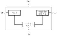
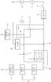
도 1을 참고하면, 본 발명에 따른 발광다이오드 구동장치의 일실시예는 발광다이오드 어레이(2), 방전스위치(11), 충전스위치(12), 블록스위치(13), 제어기(20), 충방전회로(30), 정류회로(3), 전류 또는 전압제한회로(4) 및 역률 개선 회로(7)를 포함한다.1, an LED driving apparatus according to an embodiment of the present invention includes a light emitting
본 발명에 따른 발광다이오드 구동장치의 발광다이오드 어레이(2)는 직렬로 연결된 제1발광다이오드 어레이 블록(2-1)과 제2발광다이오드 어레이 블록(2-2)을 포함한다. 220V 교류 전압에서 구동되는 경우를 예로 들면, 제1발광다이오드 어레이 블록(2-1)의 구동전압은 약 50V이고, 제2발광다이오드 어레이 블록(2-2)의 구동전압은 약 200V일 수 있다. 제1발광다이오드 어레이 블록(2-1)과 제2발광다이오드 어레이 블록(2-2)은 직렬, 병렬 또는 직병렬로 연결된 하나 이상의 발광다이오드를 포함할 수 있다.The light emitting
본 발명에 따른 발광다이오드 구동장치의 일실시예에서는 정류회로에서 출력되는 전압의 순시치 변화에 따라서 제2발광다이오드 어레이 블록(2-2) 또는 발광다이오드 어레이(2) 전체가 구동된다.In the embodiment of the LED driving apparatus according to the present invention, the second light emitting diode array block 2-2 or the light emitting
순시치가 미리 정해진 값(Vt) 이상인 B구간에서는 순시치가 증가함에 따라서 점등되는 발광다이오드 어레이 블록의 수가 증가하고, 순시치가 감소함에 따라서 점등되는 발광다이오드 어레이 블록의 수가 감소한다. 즉, 제2발광다이오드 어레이 블록(2-2)이 점등된 후 순시치가 증가함에 따라서 발광다이오드 어레이(2) 전체가 점등된다. 그리고 다시 순시치가 감소함에 따라서 제1발광다이오드 어레이 블록(2-1)이 소등되고, 제2발광다이오드 어레이 블록(2-2)만 점등된 상태를 유지한다. 여기서 Vt 값은 제2발광다이오드 어레이 블록(2-2)을 구동시킬 수 있는 최소 전압 값일 수 있다.In the section B where the instantaneous value is equal to or greater than the predetermined value Vt, the number of light emitting diode array blocks to be lit increases as the instantaneous value increases, and the number of light emitting diode array blocks that are lit as the instantaneous value decreases decreases. That is, as the instantaneous value increases after the second light emitting diode array block 2-2 is turned on, the entire light emitting
순시치가 미리 정해진 값(Vt) 미만인 A구간에서는 정류회로에서 출력되는 전압에 의해서 발광다이오드 어레이 블록이 점등되지 않는다. A구간에서는 순시치가 낮아서 정류회로에서 출력되는 전압에 의해서 제2발광다이오드 어레이 블록(2-2)이 점등되지 않는다. A구간에서의 순시치는 제1발광다이오드 어레이 블록(2-1)은 점등할 수 있는 값 이상이 될 수 있으나, 도 1에 도시된 바와 같이, 회로의 구성상 제1발광다이오드 어레이 블록(2-1)에만 정류회로(3)에서 출력되는 전압이 인가될 수 없으므로, 순시치가 A구간에 도달하면, 발광다이오드 어레이(2) 전체가 소등된다. 그리고 일정한 시간이 경과한 후 충방전회로(30)에서 공급된 전기에너지에 의해서 발광다이오드 어레이 전체(2) 또는 제2발광다이오드 어레이 블록(2-2)이 점등된 후 다시 꺼진다. 블록스위치(13)가 온 상태인 경우에는 제2발광다이오드 어레이 블록(2-2)만 점멸하며, 오프 상태인 경우에는 발광다이오드 어레이 전체(2)가 점멸한다.In the section A where the instantaneous value is less than the predetermined value Vt, the light emitting diode array block is not turned on by the voltage outputted from the rectifying circuit. In the period A, the instantaneous value is low and the second light emitting diode array block 2-2 is not turned on by the voltage outputted from the rectifying circuit. The instantaneous value in the period A may be equal to or greater than a value that allows the first light emitting diode array block 2-1 to be turned on. However, as shown in FIG. 1, the first light emitting diode array block 2- 1, the voltage output from the rectifying
본 발명에 따른 발광다이오드 구동장치는 정류회로(3)와 연결된 충방전회로(30)의 충전시점과 방전시점을 효과적으로 제어하여, 정류회로(3)에서 출력되는 전압의 순시치가 A구간에 속하는 경우에도 발광다이오드 어레이(2)가 적어도 한번 점멸되도록 한다. 이를 통해서, 발광다이오드 이용효율(발광다이오드 실효 소비전력/직류정격 전류 구동시의 발광다이오드 소비전력)을 높일 수 있으며, 플리커 현상을 개선하고, 시인성을 향상시킬 수 있다.The LED driving apparatus according to the present invention effectively controls the charging time point and the discharging time point of the charging and discharging
정류회로(3)는 입력되는 교류 전압을 전파 정류하는 역할을 한다. 정류회로(3)는 브리지 다이오드 회로일 수 있다. 정류회로(3)는 도 1에 도시된 바와 같이 교류 전압원(1)에 접속된다.The rectifying
스위치들(11, 12, 13)은 MOSFET(Metal Oxide Semiconductor Field Effect Transistor) 소자 등으로 구성할 수 있다. 충방전회로(30)와 발광다이오드 어레이(2)의 전단을 연결하는 경로에 설치되는 방전스위치(11)와 정류회로(3)의 출력단과 충방전회로(30)를 연결하는 경로에 설치되는 충전스위치(12)는 충방전회로(30)의 방전시점과 충전시점을 조절하기 위해서 사용된다. 충전시점을 조절함으로써 정류회로(3) 출력단에 흐르는 전류 파형을 전압 파형에 가깝게 조절할 수 있으며, 고조파 왜곡률을 낮출 수 있다. 방전시점을 조절함으로써, A구간에서 발광다이오드 어레이(2) 전체 또는 일부 블록이 적어도 한번 점멸되도록 한다.The
충전스위치(12)가 온되면 정류회로(3)의 출력단과 충방전회로(30)가 연결되면서 충방전회로(30)에서 충전이 일어나며, 방전스위치(11)가 온되면 충방전회로(3)와 발광다이오드 어레이(2)가 연결되고, 충방전회로(30)에서 방전이 일어나 발광다이오드 어레이(2) 측에 전원이 공급된다.When the
블록스위치(13)는 제1발광다이오드 어레이 블록(2-1)의 바이패스 경로(8)에 설치된다. 본 실시예에서는 블록스위치(13)와 바이패스 경로(8)가 블록스위치 회로를 구성한다. 블록스위치(13)가 오프되면 발광다이오드 어레이(2) 전체에 전류가 흐른다. 블록스위치(13)가 온되면 제2발광다이오드 어레이 블록(2-2)에만 전류가 흐른다. 즉, 블록스위치(13)는 제2발광다이오드 어레이 블록(2-2)에만 전류가 흐르도록 할지 발광다이오드 어레이(2) 전체에 전류가 흐르도록 할지 여부를 결정하는 역할을 한다. 블록스위치 회로는 도 1에 도시된 형태와 같이 바이패스 라인에 스위치를 설치하는 방법 이외에 소자들을 연결하는 라인에 하나 또는 복수의 스위칭 소자를 설치하여 다양한 형태로 구성할 수 있다.The
제어기(20)는 정류회로(3)에서 출력되는 전압의 크기 또는 위상을 확인하여, 방전스위치(11)와 충전스위치(12)를 제어함으로써, 방전시점과 충전시점을 제어한다.The
또한, 제어기(20)는 블록스위치(13)의 온/오프 시간을 제어한다. 정류회로(3) 또는 충방전회로(30)에서 출력되는 전압의 크기가 발광다이오드 어레이(2)의 구동전압 이상인 경우에는 블록스위치(13)를 오프하여 바이패스 경로(8)를 차단함으로써, 발광다이오드 어레이(2) 전체에 전류가 흐르도록 한다.In addition, the
도 2는 도 1에 도시된 제어기의 일실시예의 블록도이다. 도 2를 참고하면, 제어기(20)는 전압 또는 위상 검출회로(22) 및/또는 스위치제어부(23) 및/또는 메모리(21)를 포함할 수 있다. 전압검출회로는 정류회로(3)에서 출력되는 전압의 순시치가 어느 범위에 속하는지를 확인한다. 전압검출회로는 전자회로 분야에서 널리 쓰이는 다양한 회로를 사용할 수 있다. 예를 들면, 복수의 OP 앰프를 이용한 전압 비교기 등을 사용할 수 있다. 제어기(20)에는 전압을 직접 검출하는 전압검출회로 대신에 위상검출회로를 사용할 수 있다. 위상검출회로는 전압의 순시치가 0이 되는 순간을 검출할 수 있는 제로크로스 검출기 등을 이용하여 구성할 수 있다. 정류회로(3)에서 출력되는 전압은 위상에 따라서 순시치가 변하므로 위상의 변화를 통해서 순시치의 변화를 알 수 있다. 입력 전원이 불안정한 경우에는 전압검출회로를 사용하는 것이 바람직하다.2 is a block diagram of one embodiment of the controller shown in FIG. 2, the
메모리(21)에는 정류회로(3)에서 출력되는 전압의 크기에 따라서 스위치들(11, 12, 13)을 구동하기 위한 구동 데이터가 저장되어 있다. 구동 데이터는 발광다이오드의 수 및 구동전압, 요구되는 발광다이오드 어레이의 점멸주파수 등에 따라서 정해진다.The
메모리를 사용하지 않고 채널별로 검출된 전압 또는 위상에 따라, 혹은, 타이머와 같은 카운터 소자를 이용하여 스위치들(11, 12, 13)을 제어할 수도 있다.It is also possible to control the
충방전회로(30)는 B구간에서 정류회로(3)의 출력전압에 의해서 충전된 후 A구간에서 방전되면서, 발광다이오드 어레이(2)에 전원을 인가하는 역할을 한다. 본 실시예에 있어서, 충방전회로(30)의 일 예로 커패시터를 사용한다. 충전스위치(12)가 온되면, 충방전회로(30)가 정류회로(3)와 연결되어 충방전회로(30)에 전기에너지가 저장된다. 방전스위치(11)가 온되면, 충방전회로(30)가 발광다이오드 어레이(2) 측과 연결되고 충방전회로(30)에서 방전이 일어나 발광다이오드 어레이(2) 측에 전원이 공급된다. 충방전회로(30)로는 인덕터를 사용할 수도 있다.The charge /
전류제한회로 또는 전압제한회로(4)는 부하에 걸리는 전류 또는 전압을 제한하는 역할을 한다. 전류제한회로 또는 전압제한회로는 발광다이오드 어레이(2)에 과도한 전류가 흐르는 것을 방지하기 위한 것으로서, 발광다이오드 어레이(2)에 직렬로 연결된다. 전류제한회로는 저항, 커패시터, 바이폴라 트랜지스터, 모스 트랜지스터 등으로 구현할 수 있다. 또한, 전계효과 트랜지스터(FET) 혹은 트랜지스터(TR)와 보조소자의 조합으로 구현하는 방법, 그리고 OP AMP 혹은 레귤레이터 등 집적회로를 이용하는 방법 등으로 구현할 수 있다.The current limiting circuit or the
본 발명에 따른 발광다이오드 구동장치는 서지전압으로부터 발광다이오드 구동장치를 보호하기 위한 저항(6), 서지억제소자(미도시), 퓨즈(5) 등으로 구성한 서지보호회로를 더 포함할 수 있다.The light emitting diode driving apparatus according to the present invention may further include a surge protection circuit composed of a
또한, 정류회로(3)의 출력단에 흐르는 전류 파형과 전압 파형의 차이를 최소화하기 위해서, 에너지를 저장하거나, 소비하도록 구성된 역률 개선 회로(7)를 더 포함할 수 있다. 이 회로는 저항이나 커패시터 등과 스위치로 이루어질 수 있다. 예를 들어, 정류회로(3)에 병렬로 연결된 저항과 저항과 정류회로(3)를 연결하는 경로에 설치된 스위치로 이루어질 수 있다. 전류 파형과 전압 파형의 차이가 큰 구간, 예를 들어 A구간 및 B구간 초기에 스위치를 온하면, 정류회로(3)의 출력단의 전압이 저항에 인가되고, 저항에 그 전압에 비례하여 사인파 형태로 전류가 흐른다. A구간에서는 발광다이오드 어레이(2)로는 전류가 흐르지 않으므로, 이 저항에 흐르는 전류가 정류회로(3)의 출력단에 흐르는 전류가 된다. 이와 같은 방법으로, 정류회로(3)의 출력단의 전류의 형태를 전압의 형태와 거의 일치시킴으로써 역률을 개선할 수 있으며, A구간에서 B구간으로 넘어가면서, 제2발광다이오드 어레이 블록(2-2)으로 갑자기 많은 전류가 흘러, 정류회로(3)의 출력단의 전류 파형에 고조파 성분이 많이 생기는 것도 방지할 수 있다.Further, the
역률 개선 회로(7)로 에너지를 저장할 수 있는 커패시터 등을 사용하는 경우에는 저장된 에너지를 제어기(20) 및 스위치들(11, 12, 13)의 구동 전원을 공급하는 용도로 활용할 수 있다.In the case where a capacitor or the like capable of storing energy is used as the power
또한, 본 발명에 따른 발광다이오드 구동장치의 일실시예는 발광다이오드 어레이(2)를 펄스 구동하는 역할을 하는 점멸스위치(14)를 더 포함할 수 있다. 점멸스위치(14)는 발광다이오드 어레이(2)의 점멸주파수를 변경하는 역할을 한다. 점멸스위치(14)의 온/오프가 반복되는 경우에는 제2발광다이오드 어레이 블록(2-2) 또는 전체 발광다이오드 어레이(2)가 펄스 전압에 의해서 구동되며, 점멸스위치(14)가 온되는 시간과 오프되는 시간을 조절함으로써, 펄스 전압의 형태가 결정된다.The LED driving apparatus according to an embodiment of the present invention may further include a
점멸스위치(14)는 구동단의 전압이 피크치일 때 발광다이오드 어레이에 흐르는 전류를 차단하는 OVP(over-voltage protection)소자의 역할을 할 수도 있다.The
또한, 전류파형의 전체고조파 왜곡률을 줄이기 위하여 충방전회로(30)의 충전전류를 제한하도록 구성된 충전전류제한 회로(9)를 더 포함한다. 충전전류제한 회로(9)는 충방전회로(30)에 직렬로 연결되어 충방전회로(30)에 흐르는 전류를 제한한다. 충전전류제한 회로(9)는 저항, 커패시터, 바이폴라 트랜지스터, 모스 트랜지스터 등으로 구현할 수 있다.The charging current limiting
도 3의 (a)는 도 1에 도시된 발광다이오드 구동장치에서 입력원의 전압 파형과 전류 파형의 일 예를 나타낸 도면이며, 도 3의 (b)는 도 1에 도시된 발광다이오드 구동장치에서 입력원의 전압 파형과 발광다이오드 어레이에 인가되는 전류 파형의 일 예를 나타낸 도면이다. 도 3의 (a) 및 도 3의 (b)를 참고하여, 발광다이오드 구동장치의 1주기 분의 작용을 설명한다.FIG. 3 (a) is a view showing an example of a voltage waveform and a current waveform of an input source in the LED driving apparatus shown in FIG. 1. FIG. 3 (b) FIG. 7 is a diagram showing an example of a voltage waveform of an input source and a current waveform applied to the light emitting diode array. FIG. The operation of one cycle of the LED driving apparatus will be described with reference to FIGS. 3A and 3B. FIG.
제어기(20)에서 정류회로(3)에서 출력되는 전압의 순시치를 측정한 결과, A구간에 속하는 것으로 판단된 경우에는, 제어기(20)가 방전스위치(11)와 충전스위치(12)는 오프하고, 블록스위치(13)는 온한다(아직 충전되기 전이므로 방전스위치(11)를 온하여도 방전되지 않는다). If the instantaneous value of the voltage output from the
A구간에서는, 도 3의 (b)에 도시된 바와 같이, 제2발광다이오드 어레이 블록(2-2)에 전류가 흐르지 않는다. 그리고 도 3의 (a)에 도시된 바와 같이 역률 개선 회로(7)에는 전압파형과 유사한 사인파 형태의 전류가 흐른다.In the section A, no current flows in the second light emitting diode array block 2-2 as shown in Fig. 3 (b). As shown in Fig. 3 (a), a sinusoidal current similar to the voltage waveform flows in the power
정류회로(3)에서 출력되는 전압의 크기가 Vt 이상인 B구간에 도달하면, 정류회로(3)에서 출력된 전압에 의해서 제2발광다이오드 어레이 블록(2-2)이 점등될 수 있으므로, 제2발광다이오드 어레이 블록(2-2)이 켜진다. 바이패스 경로(8)의 블록스위치(13)가 온되어 있으므로, 제1발광다이오드 어레이 블록(2-1)에는 전류가 흐르지 않는다. 도 3의 (b)에 도시된 바와 같이, 제2발광다이오드 어레이 블록(2-2)에 흐르는 전류는 정류회로(3)에서 출력되는 전압의 크기가 증가함에 따라서 증가하지만 전압/전류 제한회로(4)에 의해서 일정한 수준 이상으로 증가하지 않는다.The second light emitting diode array block 2-2 can be turned on by the voltage outputted from the rectifying
정류회로(3)에서 출력되는 전압의 크기가 발광다이오드 어레이(2) 전체를 점등시킬 수 있는 값(Va) 이상이 되면 제어기(20)는 블록스위치(13)를 오프시킨다. 바이패스 경로의 블록스위치(13)가 오프되었으므로, 발광다이오드 어레이(2) 전체가 켜진다. 이때, 도 3의 (b)에 도시된 바와 같이, 발광다이오드 어레이(2)에는 전압/전류 제한회로(4)에 의해서 제한된 전류가 계속 흐른다.The
제어기는 B구간의 일정한 시점에 충전스위치(12)를 온시켜, 충방전회로(30)에 전류가 흐르도록 한다. 이때, 도 3의 (a)에 도시된 바와 같이, 회로의 입력단에 흐르는 전류 값이 커진다. 발광다이오드 어레이(2)에 흐르는 전류는 전류 또는 전압제한회로(4)에 의해서 제한되어 일정하지만, 회로의 입력단에 흐르는 전류 값은 충방전회로(30)에 흐르는 전류 값만큼 증가한다. 충방전회로(30)에 흐르는 전류 값은 충전전류제한회로(9)에 의해서 제한된다. 이와 같은 방법으로 회로의 전류 파형을 입력 전압 파형에 근접시킴으로써, 전류 파형의 전체 고주파 왜곡률(THD, Total harmonic distortion)을 줄이고, 역률을 개선할 수 있다. 충전스위치(12)를 온하는 시점과 오프하는 시점 및 충전전류의 양은 전류 파형을 입력 전압 파형에 근접시키기 위해서 B구간 내에서 조절이 가능하다.The controller turns on the charging
정류회로(3)에서 출력되는 전압의 크기가 다시 Va미만인 구간에 도달하면, 제어기(20)는 다시 블록스위치(13)를 온하여 제2발광다이오드 어레이 블록(2-2)에만 전류가 흐르도록 한다.The
정류회로(3)에서 출력되는 전압의 크기가 다시 A구간에 도달하면, 제어기(20)는 일정 시간 경과 후 방전스위치(11)를 온하여 커패시터에 충전된 전기에너지를 발광다이오드 어레이(2)에 공급하여 발광다이오드 어레이(2)가 꺼졌다 켜지도록 한다. 그리고 다시 방전스위치(11)를 오프하여 발광다이오드 어레이(2)가 꺼지도록 한다. 이때, 방전을 개시하고 중지하는 시점은 발광다이오드 어레이(2)의 순전압, 충전용량, 입력원의 전압변동 및 설정 구동 주파수 등의 변수에 연동하여 결정한다. 방전 개시시점과 중지시점을 조절하여 A구간에서 발광다이오드 어레이(2) 전체가 꺼져있는 시간과 켜져 있는 시간을 조절할 수 있다.When the magnitude of the voltage output from the rectifying
도 3의 (a)와 3b에 도시된 바와 같이, 이때, 입력단에는 전류가 거의 흐르지 않지만, 발광다이오드 어레이(2)에는 충방전회로(30)에서 공급된 전기에너지에 의한 전류가 흐른다.As shown in Figs. 3 (a) and 3 (b), at this time, a current hardly flows through the input terminal, but a current due to the electric energy supplied from the charging / discharging
도 4의 (a)는 도 1에 도시된 발광다이오드 구동장치에서 입력원의 전압 파형과 전류 파형의 다른 예를 나타낸 도면이며, 도 4의 (b)는 도 1에 도시된 발광다이오드 구동장치에서 입력원의 전압 파형과 발광다이오드 어레이에 인가되는 전류 파형의 다른 일 예를 나타낸 도면이다. 본 예에서는 B구간에서 발광다이오드 어레이(2)가 점멸하여 발광다이오드 어레이(2)의 점멸주파수가 240㎐ 이상으로 증가하였다.FIG. 4 (a) is a view showing another example of a voltage waveform and a current waveform of an input source in the LED driving apparatus shown in FIG. 1. FIG. 4 (b) FIG. 5 is a view showing another example of a voltage waveform of an input source and a current waveform applied to the light emitting diode array. FIG. In this example, the light emitting
방전스위치(11), 충전스위치(12)의 동작은 도 3의 (a) 및 도 3의 (b)에 도시된 바와 동일하므로, 점멸스위치(14)의 B구간에서의 동작과 블록스위치(13)의 A구간에서의 동작에 대해서만 설명한다.The operations of the
정류회로(3)에서 출력되는 전압의 크기가 B구간 중 발광다이오드 어레이(2)를 소등시키고자 하는 구간에 도달하면, 점멸스위치(14)를 오프시키고, 일정한 시간 경과 후 다시 온시킨다. B구간에서 한번 점멸시킨 경우에는 도 4에 도시된 바와 같이, 점멸주파수가 360㎐로 증가한다.When the magnitude of the voltage outputted from the rectifying
점멸주파수를 더욱 증가시킬 필요가 있는 경우에는 B구간에서 점멸 횟수를 증가시킬 수 있다. 이때, 점멸스위치(14)가 온/오프되는 시간을 조절하면, 듀티사이클과 주파수도 조절할 수 있다. 점멸스위치(14)가 온/오프되는 시간은 부하에 인가되는 평균 전력의 크기가 일정하도록 조정하는 것이 바람직하다. 전압의 크기가 작은 구간에서는 점멸스위치(14)의 온 시간을 길게 하고, 전압의 크기가 큰 경우에는 점멸스위치(14)의 온 시간을 짧게 하면 부하에 인가되는 평균 전력의 크기를 일정하게 할 수 있다.If it is necessary to further increase the flicker frequency, the number of flicker can be increased in the section B. At this time, the duty cycle and the frequency can be adjusted by adjusting the ON / OFF time of the
정류회로(3)에서 출력되는 전압의 크기가 A구간 도달하면, 본 실시예에서는 블록스위치(13)의 온 상태가 유지된다. 따라서 A구간에서 발광다이오드 어레이(2) 전체가 아닌 제2발광다이오드 어레이 블록(2-2)만이 점멸한다. 충전전류의 제한으로 충방전회로(30)에 충전된 전압이 전체 발광다이오드 어레이(2)를 점등시키기에 부족한 경우에는 이와 같이, A구간에서 블록스위치(13)를 온하여 제1발광다이오드 어레이 블록(2-1)을 바이패스하도록 할 수 있다.When the magnitude of the voltage output from the rectifying
도 4의 (a)에는 점멸스위치(14)를 오프하는 시점에 발광다이오드 어레이(2)에 흐르는 전류가 차단되므로 입력원의 전류 값이 감소하는 것으로 도시되어 있다. 그러나 전체고조파 왜곡률을 줄이기 위하여 점멸스위치(14)가 오프되는 구간에 충방전회로(30)에 흐르는 전류를 증가시키는 방법으로 전류 파형을 조절할 수도 있다. 예를 들어, 충전전류 제한회로(9)의 전류제한 값을 조절하여 점멸스위치(14)가 오프되는 구간에 충방전회로(30)에 흐르는 전류를 증가시킬 수 있다.In FIG. 4 (a), the current flowing through the light emitting
도 5는 본 발명에 따른 발광다이오드 구동장치의 다른 실시예를 개략적으로 나타낸 도면이다.5 is a diagram schematically showing another embodiment of the LED driving apparatus according to the present invention.
본 실시예는 도 1에 도시된 실시예와 블록스위치(13)의 제어방법에 있어서 차이가 있으므로 여기에 대해서만 상세히 설명한다. 도 1에 도시된 실시예에서는 정류회로(3)에서 출력된 전압의 순시치의 변화를 제어기(20)에서 검출하여 바이패스 경로(8)의 블록스위치(13)를 제어하였다. 그러나 본 실시예에서는 제1발광다이오드 어레이 블록(2-1)에 직렬로 설치된 전류 검출회로(25)에서 검출된 전류 값을 이용하여 블록스위치(13)를 제어한다는 점에서 차이가 있다. 도 5에서는 제1발광다이오드 어레이 블록(2-1)에 직렬로 설치된 전류 검출회로(25)를 이용하는 것으로 설명하였으나, 제1발광다이오드 어레이 블록(2-1)에 병렬로 설치된 전압 검출회로에서 검출된 전압 값을 이용하여 블록스위치(13)를 제어할 수도 있다.The present embodiment differs from the embodiment shown in Fig. 1 in the control method of the
정류회로(3)에서 출력된 전압이 증가하면, 바이패스 경로(8)의 저항(10)에 흐르는 전류가 점점 증가한다. 정류회로(3)에서 출력된 전압의 크기가 점점 커져서, 바이패스 경로(8)의 저항(10)에 인가되는 전압이 제1발광다이오드 어레이 블록(2-1)의 구동전압 이상인 일정한 전압이 되면, 저항(10)과 병렬로 연결되어 있는 제1발광다이오드 어레이 블록(2-1) 및 전류 검출회로(25)에도 전류가 흐른다. 전류 검출회로(25)에 전류가 흘러, 전류 검출회로(25)가 블록스위치(13)에 검출신호를 송신하면, 블록스위치(13)가 오프되어 바이패스 경로(8)가 차단됨으로써, 발광다이오드 어레이(2) 전체에 전류가 흐르게 된다.When the voltage output from the rectifying
도 6은 본 발명에 따른 발광다이오드 구동장치의 또 다른 실시예를 개략적으로 나타낸 도면이다.FIG. 6 is a schematic view illustrating another embodiment of the LED driving apparatus according to the present invention.
본 실시예에서는 정류회로(3)에서 출력되는 전압의 순시치 변화에 따라서 직렬로 연결된 제1발광다이오드 어레이 블록(2-1)과 제2발광다이오드 어레이 블록(2-2)을 선택적으로 구동하는 방법에 있어서, 도 1에 도시된 실시예와 차이가 있으므로, 여기에 대해서만 상세히 설명한다. 즉, 블록스위치(15)의 구성에 있어서, 도 1에 도시된 실시예와 차이가 있다.In this embodiment, the first light emitting diode array block 2-1 and the second light emitting diode array block 2-2, which are connected in series according to the instantaneous value of the voltage output from the rectifying
본 실시예는 도 1에 도시된 실시예와 달리, 정류회로(3)의 출력 측과 제2발광다이오드 어레이 블록(2-2)의 전단을 연결하는 경로를 구비하여, 이 경로에 블록스위치(15)가 설치된다.The present embodiment differs from the embodiment shown in Fig. 1 in that a path connecting the output side of the
본 실시예에 있어서, 제어기(20)는 B구간에서 블록스위치(15)를 온하여, 제2발광다이오드 어레이 블록(2-2)에만 전류가 흐르도록 한다. 전압이 증가하여 발광다이오드 어레이(2) 전체를 점등할 수 있는 수준이 되면 블록스위치(15)를 오프하여, 발광다이오드 어레이(2) 전체에 전류가 흐르도록 한다. A구간에서는 블록스위치(15)를 오프하고, 방전스위치(11)를 온하여, 충방전회로(30)의 전기에너지에 의해서 발광다이오드 어레이(2) 전체에 전류가 흐르도록 한다. 점멸스위치(14)는 전 구간에서 계속 온되어 있을 수 있으며, 점멸주파수를 변경할 경우에는 B구간에서 온오프가 반복될 수 있다.In the present embodiment, the
도 7은 본 발명에 따른 발광다이오드 구동장치의 또 다른 실시예를 개략적으로 나타낸 도면이다.FIG. 7 is a schematic view illustrating another embodiment of the LED driving apparatus according to the present invention. Referring to FIG.
본 실시예의 경우에는 충방전회로(30)와 직렬로 연결된 방전스위치(27)가 충전스위치의 역할을 동시에 수행한다. 즉, 방전스위치(27)를 온시키면 충전이 진행되고, 오프시키면 충전이 중지된다. 그리고 충전이 된 상태에서 다시 방전스위치(27)를 온시키면 방전이 진행되고, 오프시키면 방전이 중지된다.In the case of this embodiment, the discharging
도 8의 (a)는 도 7에 도시된 발광다이오드 구동장치에서 입력원의 전압 파형과 전류 파형의 일 예를 나타낸 도면이며, 도 8의 (b)는 도 7에 도시된 발광다이오드 구동장치에서 입력원의 전압 파형과 발광다이오드 어레이에 인가되는 전류 파형의 일 예를 나타낸 도면이다. 도 8의 (a) 및 도 8의 (b)를 참고하여, 발광다이오드 구동장치의 1주기 분의 작용을 설명한다.FIG. 8A is a diagram showing an example of a voltage waveform and a current waveform of an input source in the LED driving apparatus shown in FIG. 7, and FIG. 8B is a diagram showing an example of a voltage waveform and a current waveform of the light emitting diode driving apparatus shown in FIG. FIG. 7 is a diagram showing an example of a voltage waveform of an input source and a current waveform applied to the light emitting diode array. FIG. The operation of one cycle of the LED driving apparatus will be described with reference to Figs. 8 (a) and 8 (b).
제어기(20)에서 정류회로(3)에서 출력되는 전압의 크기를 측정한 결과, 제2발광다이오드 어레이 블록(2-2)의 구동전압 미만인 A구간에 속하는 것으로 판단된 경우에는, 제어기(20)가 방전스위치(27)는 오프하고, 블록스위치(13)는 온한다. If it is determined that the voltage of the voltage output from the
제2발광다이오드 어레이 블록(2-2)의 구동전압 미만이므로, 도 8의 (b)에 도시된 바와 같이, 제2발광다이오드 어레이 블록(2-2)에 전류가 흐르지 않는다. 그리고 도 8의 (a)에 도시된 바와 같이 역률 개선 회로(7)에 사인파 형태의 전류가 흐른다.The current does not flow to the second light emitting diode array block 2-2 as shown in FIG. 8 (b) because it is less than the driving voltage of the second light emitting diode array block 2-2. Then, a sinusoidal current flows in the power
정류회로(3)에서 출력되는 전압의 크기가 제2발광다이오드 어레이 블록(2-2)의 구동전압 범위인 B구간에 도달하면, 정류회로(3)에서 출력된 전압이 제2발광다이오드 어레이 블록(2-2)의 구동전압 이상이므로, 제2발광다이오드 어레이 블록(2-2)이 켜진다. 바이패스 경로(8)의 블록스위치(13)가 온되어 있으므로, 제1발광다이오드 어레이 블록(2-1)에는 전류가 흐르지 않는다. 제2발광다이오드 어레이 블록(2-2)에 흐르는 전류는 정류회로(3)에서 출력되는 전압의 크기가 증가함에 따라서 증가하지만 전압/전류 제한회로(4)에 의해서 일정한 수준 이상으로 증가하지 않는다.When the voltage output from the rectifying
정류회로(3)에서 출력되는 전압의 크기가 발광다이오드 어레이(2) 전체를 점등할 수 있는 구간에 도달하면, 제어기(20)는 블록스위치(13)는 오프시킨다. 바이패스 경로의 블록스위치(13)가 오프되었으므로, 발광다이오드 어레이(2) 전체가 켜진다. 이때, 도 8의 (b)에 도시된 바와 같이, 발광다이오드 어레이(2)에는 전압/전류 제한회로(4)에 의해서 제한된 전류가 흐른다.The
그리고 B구간의 방전스위치(27)가 온된 시점부터는 충방전회로(30)에도 전류가 흐른다. 따라서 도 8의 (a)에 도시된 바와 같이, 회로의 입력단에 흐르는 전류 값이 커진다. 발광다이오드 어레이(2)에 흐르는 전류는 전류 또는 전압제한회로(4)에 의해서 제한되어 일정하게 유지되지만, 회로의 입력단에 흐르는 전류 값은 충방전회로(30)에 흐르는 전류 값만큼 증가한다. 충방전회로(30)에 흐르는 전류 값은 충전전류제한회로(9)에 의해서 제한된다.When the discharging
정류회로(3)에서 출력되는 전압의 크기가 다시 감소하면, 제어기(20)는 다시 블록스위치(13)를 온하여 제2발광다이오드 어레이 블록(2-2)에만 전류가 흐르도록 한다.When the magnitude of the voltage output from the rectifying
B구간에서 방전스위치(27)가 오프되면, 충방전회로(30)는 제2발광다이오드 어레이 블록(2-2)과 분리되어 전기에너지가 저장된 상태로 유지된다.When the discharging
정류회로(3)에서 출력되는 전압의 크기가 다시 A구간에 도달하면, 제어기(20)는 일정 시간 경과 후 방전스위치(27)를 온하여 커패시터에 충전된 전기에너지를 발광다이오드 어레이(2)에 공급하여 발광다이오드 어레이(2)가 꺼졌다 켜지도록 한다. 그리고 다시 방전스위치(27)를 오프하여 발광다이오드 어레이(2)가 꺼지도록 한다.When the magnitude of the voltage output from the rectifying
도 9는 본 발명에 따른 발광다이오드 구동장치의 또 다른 실시예를 개략적으로 나타낸 도면이다.FIG. 9 is a schematic view of another embodiment of the LED driving apparatus according to the present invention.
본 실시예는 발광다이오드 어레이(2)의 구성에 있어서 상술한 실시예들과 차이가 있다. 본 실시예에 있어서, 발광다이오드 어레이(2)는 3개의 블록(2-1, 2-2a, 2-2b)을 포함한다. 발광다이오드 어레이(2)는 B구간에서 정류회로(3)에서 출력되는 전압의 크기가 증가함에 따라서, 처음에는 제2발광다이오드 어레이 블록(2-2a)이 점등되고, 이후에는 제2발광다이오드 어레이 블록(2-2a)과 제3발광다이오드 어레이 블록(2-2b)이 함께 점등된다. 그리고 전압의 크기가 더욱 증가하면 전체 발광다이오드 어레이(2)가 점등된다. 즉, B구간에서 전압이 증가함에 따라서 점등되는 발광다이오드의 수가 증가한다.The present embodiment is different from the above-described embodiments in the configuration of the light-emitting
본 실시예에 있어서, B구간의 초기에는 제1블록스위치(16a)가 온되어, 제2발광다이오드 어레이 블록(2-2a)에만 전류가 흐른다. 그리고 전압이 증가하여, 제2발광다이오드 어레이 블록(2-2a)과 제3발광다이오드 어레이 블록(2-2b)이 함께 점등될 수 있는 상태가 되면, 제1블록스위치(16a)가 오프되고, 제2블록스위치(16b)가 온되어 제2발광다이오드 어레이 블록(2-2a)과 제3발광다이오드 어레이 블록(2-2b)에 전류가 흐른다. 그리고 전압이 더욱 증가하면, 제1블록스위치(16a)와 제2블록스위치(16b)가 모두 오프되어, 전체 발광다이오드 어레이(2)에 전류가 흐른다.In the present embodiment, at the beginning of the section B, the
A구간에서는 충방전회로(30)에서 출력되는 전압의 크기가 감소함에 따라서 점등되는 발광다이오드 어레이 블록의 수가 감소하도록 블록스위치들이 제어될 수 있다. 충방전회로(30)에 충분한 전기에너지가 저장된 경우에는 전체 발광다이오드 어레이(2)가 점등된 후 일정시간 경과 후 소등될 수도 있으나, 충전전류 제한에 의해서 충분한 전기에너지가 저장되지 않은 경우에는 충방전회로(30)에서 출력되는 전압의 크기가 감소함에 따라서 발광다이오드 어레이 블록의 수가 감소하고, 일정시간 경과 후 전체가 소등되도록 블록스위치들이 제어될 수 있다.The block switches can be controlled so that the number of the light emitting diode array blocks to be turned on decreases as the voltage output from the charging and discharging
도 10 내지 12는 본 발명에 따른 발광다이오드 구동장치의 또 다른 실시예들의 일부를 개략적으로 나타낸 도면이다.10 to 12 are views schematically showing a part of still another embodiment of the LED driving apparatus according to the present invention.
도 10에서는 B구간의 초기에는 제1블록스위치(17a)가 온되어, 제2발광다이오드 어레이 블록(2-2a)에만 전류가 흐른다. 그리고 전압이 증가하여, 제2발광다이오드 어레이 블록(2-2a)과 제3발광다이오드 어레이 블록(2-2b)이 함께 점등될 수 있는 상태가 되면, 제1블록스위치(17a)가 오프되고, 제2블록스위치(17b)가 온되어 제2발광다이오드 어레이 블록(2-2a)과 제3발광다이오드 어레이 블록(2-2b)에 전류가 흐른다. 그리고 전압이 더욱 증가하면, 제1블록스위치(17a)와 제2블록스위치(17b)가 모두 오프되어, 전체 발광다이오드 어레이(2)에 전류가 흐른다.In Fig. 10, the
도 11에서는 B구간의 초기에는 제1블록스위치(18a)와 제2블록스위치(18b)가 모두 온되어, 제2발광다이오드 어레이 블록(2-2a)에만 전류가 흐른다. 그리고 전압이 증가하여, 제2발광다이오드 어레이 블록(2-2a)과 제3발광다이오드 어레이 블록(2-2b)이 함께 점등될 수 있는 상태가 되면, 제1블록스위치(18a)가 오프되어 제2발광다이오드 어레이 블록(2-2a)과 제3발광다이오드 어레이 블록(2-2b)에 전류가 흐른다. 그리고 전압이 더욱 증가하면, 제1블록스위치(18a)와 제2블록스위치(18b)가 모두 오프되어, 전체 발광다이오드 어레이(2)에 전류가 흐른다.11, both the
도 12에서는 도 5에 도시된 실시예와 마찬가지로, 제3발광다이오드 어레이 블록(2-2b)과 제1발광다이오드 어레이 블록(2-1)에 흐르는 전류를 전류 검출회로(25)를 통해서 검출하여 제1블록스위치(19a)와 제2블록스위치(19b)를 제어한다는 점에서 도 10에 도시된 실시예와 차이가 있다.12, the current flowing through the third light emitting diode array block 2-2b and the first light emitting diode array block 2-1 is detected through the current detecting
이상에서 기술한 실시예들은 모든 면에서 예시적인 것이며 한정적인 것이 아닌 것으로서 이해해야만 한다. 본 발명의 범위는 상기 상세한 설명보다는 후술하는 특허청구범위에 의하여 나타내어지며, 특허청구범위의 의미 및 범위 그리고 그 등가개념으로부터 도출되는 모든 변경 또는 변형된 형태가 본 발명의 범위에 포함되는 것으로 해석되어야 한다.It should be understood that the above-described embodiments are illustrative in all aspects and not restrictive. The scope of the present invention is defined by the appended claims rather than the detailed description and all changes or modifications derived from the meaning and scope of the claims and their equivalents are to be construed as being included within the scope of the present invention do.
즉, 발광다이오드 어레이의 블록들에 선택적으로 전류를 흘리기 위한 블록스위치는 상술한 실시예외에 다양한 형태로 구현할 수 있으며, 그 변형된 형태도 본 발명의 범위에 포함된다.That is, the block switch for selectively supplying current to the blocks of the light emitting diode array can be implemented in various forms in the above-described exemplary embodiment, and its modified forms are also included in the scope of the present invention.
또한, 도 9 내지 12에는 발광다이오드 어레이가 세 개의 발광다이오드 어레이 블록을 포함하는 것으로 설명하였으나, 네 개 이상의 발광다이오드 어레이 블록을 포함할 수도 있다.9 to 12, the light emitting diode array includes three light emitting diode array blocks. However, the light emitting diode array may include four or more light emitting diode array blocks.
1: 교류 전압원2: 발광다이오드 어레이
2-1: 제1발광다이오드 어레이 블록2-2: 제2발광다이오드 블록
3: 정류회로7: 역률 개선 회로
8: 바이패스 경로9: 충전전류 제한회로
11, 27: 방전스위치12: 충전스위치
13, 15: 블록스위치14: 점멸스위치
20: 제어기25: 전류 검출회로
30: 충방전회로1: AC voltage source 2: Light emitting diode array
2-1: First light emitting diode array block 2-2: Second light emitting diode block
3: rectification circuit 7: power factor improvement circuit
8: Bypass path 9: Charge current limiting circuit
11, 27: discharging switch 12: charging switch
13, 15: Block switch 14: Flashing switch
20: controller 25: current detection circuit
30: charge / discharge circuit
Claims (7)
Translated fromKorean상기 충방전회로에 충전된 에너지가 상기 발광다이오드 어레이에 전달되는 경로를 연결 또는 차단시키도록 구성된 방전스위치와,
복수의 상기 발광다이오드 어레이 블록들 중에서 정류회로에서 출력된 전압이 전달되는 발광다이오드 어레이 블록의 수를 조절할 수 있도록 구성된 블록스위치 회로와,
상기 정류회로에서 출력된 전압의 순시치가 미리 정해진 값 미만인 A구간에서, 상기 발광다이오드 어레이 전체가 꺼진 후 상기 충방전회로가 방전되어, 상기 A구간에서 적어도 한번 발광다이오드 어레이 전체가 꺼진 후 복수의 상기 발광다이오드 어레이 블록 중 적어도 하나가 켜졌다 다시 꺼지도록 상기 방전스위치와 블록스위치 회로를 제어하는 제어기를 포함하며,
상기 제어기는 상기 정류회로에서 출력된 전압의 순시치가 상기 미리 정해진 값 이상인 B구간에서 상기 정류회로에서 출력되는 전압의 순시치가 증가함에 따라서 점등되는 상기 발광다이오드 어레이 블록의 수가 증가하도록 상기 블록스위치 회로를 제어하는 발광다이오드 구동장치.A rectifier circuit connected to the AC voltage source for full-wave rectifying the AC voltage of the AC voltage source; a light emitting diode array connected to the output side of the rectifying circuit and including a plurality of light emitting diode array blocks; And a charging / discharging circuit configured to be charged by the charging / discharging circuit,
A discharge switch configured to connect or disconnect a path through which the energy charged in the charging / discharging circuit is transferred to the light emitting diode array,
A block switch circuit configured to adjust the number of light emitting diode array blocks to which a voltage output from the rectifying circuit is transmitted among the plurality of light emitting diode array blocks;
Wherein the light emitting diode array is turned off after the instantaneous value of the voltage output from the rectifying circuit is less than a predetermined value and the charge and discharge circuit is discharged, And a controller for controlling the discharge switch and the block switch circuit so that at least one of the light emitting diode array blocks is turned on and off again,
Wherein the controller controls the block switch circuit so that the number of the light emitting diode array blocks is increased as the instantaneous value of the voltage output from the rectifying circuit increases in a section B where the instantaneous value of the voltage output from the rectifying circuit is equal to or greater than the predetermined value, The light emitting diode driving device controlling the light emitting diode.
상기 정류회로에서 출력된 전압이 상기 발광다이오드 어레이에 전달되는 경로를 연결 또는 차단시키도록 구성된 점멸스위치를 더 포함하며,
상기 제어기는 상기 B구간에서 적어도 한번 상기 발광다이오드 어레이가 점멸되도록, 상기 점멸스위치를 제어하는 발광다이오드 구동장치.The method according to claim 1,
Further comprising a flashing switch configured to connect or disconnect a path through which the voltage output from the rectifying circuit is transferred to the light emitting diode array,
Wherein the controller controls the flicker switch so that the light emitting diode array flickers at least once in the section B.
상기 정류회로에서 출력되는 전류 파형의 전체 고주파 왜곡률(THD, Total harmonic distortion)을 줄이기 위해서, 상기 정류회로의 출력 측에 연결되어, 전기에너지를 저장 또는 소비하도록 구성된 역률 개선 회로를 더 포함하는 발광다이오드 구동장치.The method according to claim 1,
Further comprising a power factor improving circuit connected to an output side of the rectifying circuit for storing or consuming electric energy for reducing a total harmonic distortion (THD) of a current waveform output from the rectifying circuit, Driving device.
상기 정류회로에서 출력된 전압이 상기 충방전회로에 전달되는 경로를 연결 또는 차단시키도록 구성된 충전스위치를 더 포함하며,
상기 제어기는 상기 정류회로에서 출력되는 전류파형의 전체고조파 왜곡률을 줄이기 위하여, 상기 B구간에서 상기 정류회로에서 출력된 전압이 상기 충방전회로에 전달되는 시점을 지연시키도록 상기 충전스위치를 제어하는 발광다이오드 구동장치.The method according to claim 1,
Further comprising a charge switch configured to connect or disconnect the path of the voltage output from the rectifying circuit to the charge / discharge circuit,
The controller controls the charging switch to delay the time point at which the voltage output from the rectifying circuit is transferred to the charging / discharging circuit in the section B in order to reduce the total harmonic distortion of the current waveform output from the rectifying circuit Diode driver.
상기 정류회로에서 출력되는 전류파형의 전체고조파 왜곡률을 줄이기 위하여 충방전회로의 충전전류를 제한하도록 구성된 충전전류제한 회로를 더 포함하는 발광다이오드 구동장치.5. The method of claim 4,
Further comprising a charge current limiting circuit configured to limit the charge current of the charge / discharge circuit to reduce the total harmonic distortion of the current waveform output from the rectifying circuit.
상기 블록스위치 회로는 복수의 상기 발광다이오드 어레이 블록 중 일부를 바이패스하는 경로와 그 경로에 설치된 블록스위치를 포함하는 발광다이오드 구동장치.The method according to claim 1,
Wherein the block switch circuit includes a path bypassing a part of the plurality of light emitting diode array blocks and a block switch provided in the path.
상기 발광다이오드 어레이 블록을 바이패스하는 경로에 설치된 저항과,
상기 발광다이오드 어레이 블록과 직렬로 연결되어 상기 발광다이오드 어레이 블록에 흐르는 전류를 검출하는 전류 검출회로 또는 상기 발광다이오드 어레이 블록과 병렬로 연결되어 상기 발광다이오드 어레이 블록에 인가되는 전압을 검출하는 전압 검출회로를 더 포함하며,
상기 제어기는 상기 전류 검출회로 또는 전압 검출회로에서 검출된 전류 또는 전압 값이 미리 정해진 값 이상이면 상기 블록스위치를 오프하도록 구성된 발광다이오드 구동장치.The method according to claim 6,
A resistor provided in a path for bypassing the light emitting diode array block,
A current detection circuit connected in series with the light emitting diode array block to detect a current flowing in the light emitting diode array block or a voltage detection circuit connected in parallel with the light emitting diode array block to detect a voltage applied to the light emitting diode array block Further comprising:
Wherein the controller turns off the block switch when the current or voltage value detected by the current detection circuit or the voltage detection circuit is equal to or greater than a predetermined value.
Applications Claiming Priority (2)
| Application Number | Priority Date | Filing Date | Title |
|---|---|---|---|
| KR1020130058456 | 2013-05-23 | ||
| KR20130058456 | 2013-05-23 |
Publications (2)
| Publication Number | Publication Date |
|---|---|
| KR20140138054A KR20140138054A (en) | 2014-12-03 |
| KR101686501B1true KR101686501B1 (en) | 2016-12-14 |
Family
ID=51933794
Family Applications (1)
| Application Number | Title | Priority Date | Filing Date |
|---|---|---|---|
| KR1020140061105AActiveKR101686501B1 (en) | 2013-05-23 | 2014-05-21 | Power supply circuit for light emitting diode |
Country Status (7)
| Country | Link |
|---|---|
| US (1) | US9451663B2 (en) |
| EP (1) | EP3001779A4 (en) |
| JP (1) | JP2016522551A (en) |
| KR (1) | KR101686501B1 (en) |
| CN (1) | CN105432149B (en) |
| TW (1) | TWI551185B (en) |
| WO (1) | WO2014189298A1 (en) |
Families Citing this family (22)
| Publication number | Priority date | Publication date | Assignee | Title |
|---|---|---|---|---|
| KR101552824B1 (en)* | 2013-02-28 | 2015-09-14 | 주식회사 실리콘웍스 | Circuit to control led lighting apparatus |
| WO2016093534A1 (en)* | 2014-12-12 | 2016-06-16 | 서울반도체 주식회사 | Led drive circuit with improved flicker performance, and led lighting device comprising same |
| US10187945B2 (en) | 2014-12-12 | 2019-01-22 | Seoul Semiconductor Co., Ltd. | LED drive circuit with improved flicker performance, and LED lighting device comprising same |
| KR102352631B1 (en) | 2015-01-30 | 2022-01-20 | 주식회사 엘엑스세미콘 | Circuit and method to control led lighting apparatus |
| JP2018060593A (en)* | 2015-02-18 | 2018-04-12 | 株式会社ステラージアLed | Driving circuit |
| CN107409452B (en)* | 2015-03-17 | 2020-03-10 | 飞利浦照明控股有限公司 | Driver with at least four different states |
| EP3284324A4 (en)* | 2015-04-09 | 2019-04-10 | Lynk Labs, Inc. | Low flicker ac driven led lighting system, drive method and apparatus |
| DE102015117481A1 (en)* | 2015-10-14 | 2017-04-20 | Atlas Elektronik Gmbh | Circuit for low-flicker and standard operation of light-emitting diodes, as well as light source and light |
| WO2017217690A1 (en)* | 2016-06-16 | 2017-12-21 | 주식회사 루멘스 | Led lighting apparatus driven by current in form of polygon |
| US9794992B1 (en)* | 2016-07-27 | 2017-10-17 | Vastview Technology Inc. | Universal method for driving LEDs using high voltage |
| FR3060934B1 (en)* | 2016-12-21 | 2020-11-27 | Aledia | OPTOELECTRONIC CIRCUIT INCLUDING LIGHT-LUMINESCENT DIODES |
| TWI640146B (en)* | 2017-02-06 | 2018-11-01 | 圓展科技股份有限公司 | Smart charging system and intelligent charging method |
| DE102017104290A1 (en) | 2017-03-01 | 2018-09-06 | Atlas Elektronik Gmbh | Light-emitting diode circuit and light |
| US10178717B2 (en)* | 2017-03-09 | 2019-01-08 | Dongming Li | Lamp-control circuit for lamp array emitting constant light output |
| WO2018206430A1 (en)* | 2017-05-12 | 2018-11-15 | Philips Lighting Holding B.V. | Led driver and lighting device |
| CN109152125A (en)* | 2017-06-28 | 2019-01-04 | 群光电能科技股份有限公司 | Light emitting device and method for driving the same |
| EP3735802A1 (en) | 2018-01-02 | 2020-11-11 | Signify Holding B.V. | A lighting drive, lighting system and control method |
| TWI670995B (en)* | 2018-05-29 | 2019-09-01 | 矽誠科技股份有限公司 | Light emitting diode driving apparatus with switch control circuit |
| US10433383B1 (en) | 2018-07-23 | 2019-10-01 | Semisilicon Technology Corp. | Light emitting diode driving apparatus with switch control circuit |
| US11013086B2 (en)* | 2018-12-12 | 2021-05-18 | i Sine Inc. | Methods and apparatus for delivery of constant magnitude power to LED strings |
| US11831237B2 (en) | 2021-12-09 | 2023-11-28 | Microsoft Technology Licensing, Llc | Power supply with power factor correction bypass |
| TWI847829B (en)* | 2023-08-07 | 2024-07-01 | 穩態光電科技股份有限公司 | LED lamps with adjustable flash frequency |
Citations (1)
| Publication number | Priority date | Publication date | Assignee | Title |
|---|---|---|---|---|
| JP2011076556A (en)* | 2009-10-02 | 2011-04-14 | Koyo Denshi Kogyo:Kk | Load drive control method |
Family Cites Families (31)
| Publication number | Priority date | Publication date | Assignee | Title |
|---|---|---|---|---|
| KR19990012879A (en)* | 1997-07-31 | 1999-02-25 | 이형도 | Power Factor Correction Circuit of Power Supply |
| US6989807B2 (en) | 2003-05-19 | 2006-01-24 | Add Microtech Corp. | LED driving device |
| US7709208B2 (en) | 2004-11-08 | 2010-05-04 | New York University | Methods for diagnosis of major depressive disorder |
| JP4581646B2 (en) | 2004-11-22 | 2010-11-17 | パナソニック電工株式会社 | Light emitting diode lighting device |
| US20060188333A1 (en) | 2005-02-14 | 2006-08-24 | Ron Hicks | Surface stripe, apparatus and method |
| KR100971757B1 (en) | 2009-02-17 | 2010-07-21 | 주식회사 루미네이처 | Led lighting apparatus |
| KR101017420B1 (en) | 2009-03-17 | 2011-02-28 | (주)씨엠시스 | Multi-axis turning device for caliper piston processing of automobile brake |
| KR20110138263A (en) | 2009-03-30 | 2011-12-26 | 바스프 에스이 | Polymerizable composition |
| JP5600456B2 (en)* | 2009-05-19 | 2014-10-01 | ローム株式会社 | Light emitting diode drive circuit, light emitting device and display device using the same, and drive circuit protection method |
| JP5471330B2 (en) | 2009-07-14 | 2014-04-16 | 日亜化学工業株式会社 | Light emitting diode drive circuit and light emitting diode lighting control method |
| JP2011035112A (en) | 2009-07-31 | 2011-02-17 | Sanyo Electric Co Ltd | Light-emitting diode driver circuit and lighting apparatus |
| WO2011030246A2 (en)* | 2009-09-09 | 2011-03-17 | Koninklijke Philips Electronics N.V. | Driving circuit for driving a plurality of light sources |
| EP2497337B1 (en) | 2009-11-05 | 2020-10-21 | eldoLAB Holding B.V. | Led driver for powering an led unit from a electronic transformer |
| WO2011058805A1 (en)* | 2009-11-13 | 2011-05-19 | 日亜化学工業株式会社 | Light-emitting diode drive device and light-emitting diode illumination control method |
| JP2011165394A (en) | 2010-02-05 | 2011-08-25 | Sharp Corp | Led drive circuit, dimming device, led illumination fixture, led illumination device, and led illumination system |
| US8299724B2 (en) | 2010-03-19 | 2012-10-30 | Active-Semi, Inc. | AC LED lamp involving an LED string having separately shortable sections |
| TWI475922B (en)* | 2010-03-22 | 2015-03-01 | Point Somee Ltd Liability Co | Apparatus, method and system for providing ac line power to lighting devices |
| US8654439B2 (en) | 2010-08-20 | 2014-02-18 | Nec Laboratories America, Inc. | Look-up table and digital transmitter based architecture for fiber nonlinearity compensation |
| KR20120018646A (en) | 2010-08-23 | 2012-03-05 | 삼성엘이디 주식회사 | Ac driving light emitting device |
| JP5733931B2 (en)* | 2010-09-10 | 2015-06-10 | 三菱電機株式会社 | Power supply device and lighting device |
| US8815671B2 (en) | 2010-09-28 | 2014-08-26 | International Business Machines Corporation | Use of contacts to create differential stresses on devices |
| KR101240522B1 (en) | 2010-10-20 | 2013-03-11 | (주) 이노비전 | Device for driving light emittiing diode |
| KR101198408B1 (en) | 2010-10-26 | 2012-11-07 | (주)로그인디지탈 | AC Direct Connection Type LED Lighting Device Having Function of Flicker Reduction and Improving Light Efficiency |
| KR101397953B1 (en)* | 2010-12-20 | 2014-05-27 | 이동원 | LED Lighting Device for dual commercial AC line supply |
| KR101189102B1 (en) | 2010-12-28 | 2012-10-10 | 주식회사 티엘아이 | LED Lighting System for improving modulation index |
| JP5942314B2 (en) | 2011-02-22 | 2016-06-29 | パナソニックIpマネジメント株式会社 | Lighting device and lighting apparatus using the same |
| KR20120104788A (en)* | 2011-03-14 | 2012-09-24 | 이승호 | Buck boost type power supply for light emission diode |
| EP2692207B1 (en) | 2011-03-28 | 2016-05-18 | Koninklijke Philips N.V. | Driving device and method for driving a load, in particular an led assembly |
| US8330390B2 (en) | 2011-04-11 | 2012-12-11 | Bridgelux, Inc. | AC LED light source with reduced flicker |
| JP5821279B2 (en)* | 2011-05-24 | 2015-11-24 | 日亜化学工業株式会社 | Light emitting diode drive device |
| CN202759632U (en)* | 2012-06-20 | 2013-02-27 | 伟思科技控股有限公司 | A driving circuit and lighting device for a light-emitting diode |
- 2014
- 2014-05-21KRKR1020140061105Apatent/KR101686501B1/enactiveActive
- 2014-05-22WOPCT/KR2014/004561patent/WO2014189298A1/enactiveApplication Filing
- 2014-05-22CNCN201480039125.3Apatent/CN105432149B/ennot_activeExpired - Fee Related
- 2014-05-22USUS14/892,719patent/US9451663B2/ennot_activeExpired - Fee Related
- 2014-05-22EPEP14801325.3Apatent/EP3001779A4/ennot_activeWithdrawn
- 2014-05-22JPJP2016515270Apatent/JP2016522551A/enactivePending
- 2014-05-23TWTW103118101Apatent/TWI551185B/ennot_activeIP Right Cessation
Patent Citations (1)
| Publication number | Priority date | Publication date | Assignee | Title |
|---|---|---|---|---|
| JP2011076556A (en)* | 2009-10-02 | 2011-04-14 | Koyo Denshi Kogyo:Kk | Load drive control method |
Also Published As
| Publication number | Publication date |
|---|---|
| EP3001779A1 (en) | 2016-03-30 |
| CN105432149B (en) | 2018-03-20 |
| US20160095179A1 (en) | 2016-03-31 |
| EP3001779A4 (en) | 2016-04-13 |
| CN105432149A (en) | 2016-03-23 |
| JP2016522551A (en) | 2016-07-28 |
| TWI551185B (en) | 2016-09-21 |
| WO2014189298A1 (en) | 2014-11-27 |
| KR20140138054A (en) | 2014-12-03 |
| TW201509230A (en) | 2015-03-01 |
| US9451663B2 (en) | 2016-09-20 |
Similar Documents
| Publication | Publication Date | Title |
|---|---|---|
| KR101686501B1 (en) | Power supply circuit for light emitting diode | |
| JP6396336B2 (en) | Power supply circuit that converts the blinking frequency of light emitting diodes | |
| TWI532412B (en) | Light-emitting diode driving apparatus | |
| CN103348767B (en) | The control of the light-emitting device of multiple series connection | |
| JP2012014879A (en) | Lighting device for semiconductor light emitting element, and luminaire using the same | |
| EP2189041A1 (en) | Led driver | |
| KR20090048100A (en) | LED Dimming Control Power Supply | |
| KR101160154B1 (en) | Unidirectional lighting emitting diode module device with reduction to harmonics distortion | |
| CN102469668B (en) | LED power supply circuit capable of being matched with electronic transformer | |
| JP2016042756A (en) | Lighting system with power failure compensation function, backup power supply, and battery discharge control unit | |
| KR101493813B1 (en) | LED illumination device with energy conservation | |
| JP5885908B2 (en) | LED drive device | |
| JP5562081B2 (en) | LED dimming method and dimming device | |
| KR20150017442A (en) | light emitting diode lighting apparatus | |
| CN107820348B (en) | Linear full-voltage variable-frequency constant-current circuit and LED lamp with same | |
| JP6186724B2 (en) | LED driving device | |
| KR102130176B1 (en) | Power supply circuit for alteration of flicker frequency of light emitting diode | |
| KR101537990B1 (en) | LED Lighting Apparatus | |
| KR102392256B1 (en) | LED Driver Circuit | |
| KR101473917B1 (en) | light emitting diode lighting apparatus | |
| JP2012195252A (en) | Lighting device and lighting fixture using the lighting device | |
| KR20180101699A (en) | Led lighting apparatus with interchangeability of fluorescent lamp |
Legal Events
| Date | Code | Title | Description |
|---|---|---|---|
| A201 | Request for examination | ||
| PA0109 | Patent application | Patent event code:PA01091R01D Comment text:Patent Application Patent event date:20140521 | |
| PA0201 | Request for examination | ||
| N231 | Notification of change of applicant | ||
| PN2301 | Change of applicant | Patent event date:20140603 Comment text:Notification of Change of Applicant Patent event code:PN23011R01D | |
| PG1501 | Laying open of application | ||
| E902 | Notification of reason for refusal | ||
| PE0902 | Notice of grounds for rejection | Comment text:Notification of reason for refusal Patent event date:20150826 Patent event code:PE09021S01D | |
| E902 | Notification of reason for refusal | ||
| PE0902 | Notice of grounds for rejection | Comment text:Notification of reason for refusal Patent event date:20160328 Patent event code:PE09021S01D | |
| E701 | Decision to grant or registration of patent right | ||
| PE0701 | Decision of registration | Patent event code:PE07011S01D Comment text:Decision to Grant Registration Patent event date:20160908 | |
| GRNT | Written decision to grant | ||
| PR0701 | Registration of establishment | Comment text:Registration of Establishment Patent event date:20161208 Patent event code:PR07011E01D | |
| PR1002 | Payment of registration fee | Payment date:20161208 End annual number:3 Start annual number:1 | |
| PG1601 | Publication of registration | ||
| FPAY | Annual fee payment | Payment date:20191209 Year of fee payment:4 | |
| PR1001 | Payment of annual fee | Payment date:20191209 Start annual number:4 End annual number:4 | |
| PR1001 | Payment of annual fee | Payment date:20200922 Start annual number:5 End annual number:5 | |
| PR1001 | Payment of annual fee | Payment date:20211130 Start annual number:6 End annual number:6 | |
| PR1001 | Payment of annual fee | Payment date:20230330 Start annual number:7 End annual number:7 | |
| PR1001 | Payment of annual fee | Payment date:20231207 Start annual number:8 End annual number:8 | |
| PR1001 | Payment of annual fee | Payment date:20241209 Start annual number:9 End annual number:9 |