KR101686199B1 - Semiconductor Package Structure - Google Patents
Semiconductor Package StructureDownload PDFInfo
- Publication number
- KR101686199B1 KR101686199B1KR1020100027467AKR20100027467AKR101686199B1KR 101686199 B1KR101686199 B1KR 101686199B1KR 1020100027467 AKR1020100027467 AKR 1020100027467AKR 20100027467 AKR20100027467 AKR 20100027467AKR 101686199 B1KR101686199 B1KR 101686199B1
- Authority
- KR
- South Korea
- Prior art keywords
- housing
- chip
- semiconductor
- base
- package
- Prior art date
- Legal status (The legal status is an assumption and is not a legal conclusion. Google has not performed a legal analysis and makes no representation as to the accuracy of the status listed.)
- Active
Links
Images


Classifications
- H—ELECTRICITY
- H01—ELECTRIC ELEMENTS
- H01L—SEMICONDUCTOR DEVICES NOT COVERED BY CLASS H10
- H01L25/00—Assemblies consisting of a plurality of semiconductor or other solid state devices
- H01L25/03—Assemblies consisting of a plurality of semiconductor or other solid state devices all the devices being of a type provided for in a single subclass of subclasses H10B, H10D, H10F, H10H, H10K or H10N, e.g. assemblies of rectifier diodes
- H01L25/10—Assemblies consisting of a plurality of semiconductor or other solid state devices all the devices being of a type provided for in a single subclass of subclasses H10B, H10D, H10F, H10H, H10K or H10N, e.g. assemblies of rectifier diodes the devices having separate containers
- H01L25/105—Assemblies consisting of a plurality of semiconductor or other solid state devices all the devices being of a type provided for in a single subclass of subclasses H10B, H10D, H10F, H10H, H10K or H10N, e.g. assemblies of rectifier diodes the devices having separate containers the devices being integrated devices of class H10
- H—ELECTRICITY
- H01—ELECTRIC ELEMENTS
- H01L—SEMICONDUCTOR DEVICES NOT COVERED BY CLASS H10
- H01L21/00—Processes or apparatus adapted for the manufacture or treatment of semiconductor or solid state devices or of parts thereof
- H01L21/67—Apparatus specially adapted for handling semiconductor or electric solid state devices during manufacture or treatment thereof; Apparatus specially adapted for handling wafers during manufacture or treatment of semiconductor or electric solid state devices or components ; Apparatus not specifically provided for elsewhere
- H01L21/683—Apparatus specially adapted for handling semiconductor or electric solid state devices during manufacture or treatment thereof; Apparatus specially adapted for handling wafers during manufacture or treatment of semiconductor or electric solid state devices or components ; Apparatus not specifically provided for elsewhere for supporting or gripping
- H01L21/6835—Apparatus specially adapted for handling semiconductor or electric solid state devices during manufacture or treatment thereof; Apparatus specially adapted for handling wafers during manufacture or treatment of semiconductor or electric solid state devices or components ; Apparatus not specifically provided for elsewhere for supporting or gripping using temporarily an auxiliary support
- H—ELECTRICITY
- H01—ELECTRIC ELEMENTS
- H01L—SEMICONDUCTOR DEVICES NOT COVERED BY CLASS H10
- H01L23/00—Details of semiconductor or other solid state devices
- H01L23/28—Encapsulations, e.g. encapsulating layers, coatings, e.g. for protection
- H01L23/31—Encapsulations, e.g. encapsulating layers, coatings, e.g. for protection characterised by the arrangement or shape
- H01L23/3107—Encapsulations, e.g. encapsulating layers, coatings, e.g. for protection characterised by the arrangement or shape the device being completely enclosed
- H01L23/3121—Encapsulations, e.g. encapsulating layers, coatings, e.g. for protection characterised by the arrangement or shape the device being completely enclosed a substrate forming part of the encapsulation
- H01L23/3128—Encapsulations, e.g. encapsulating layers, coatings, e.g. for protection characterised by the arrangement or shape the device being completely enclosed a substrate forming part of the encapsulation the substrate having spherical bumps for external connection
- H—ELECTRICITY
- H01—ELECTRIC ELEMENTS
- H01L—SEMICONDUCTOR DEVICES NOT COVERED BY CLASS H10
- H01L24/00—Arrangements for connecting or disconnecting semiconductor or solid-state bodies; Methods or apparatus related thereto
- H01L24/01—Means for bonding being attached to, or being formed on, the surface to be connected, e.g. chip-to-package, die-attach, "first-level" interconnects; Manufacturing methods related thereto
- H01L24/10—Bump connectors ; Manufacturing methods related thereto
- H01L24/15—Structure, shape, material or disposition of the bump connectors after the connecting process
- H01L24/16—Structure, shape, material or disposition of the bump connectors after the connecting process of an individual bump connector
- H—ELECTRICITY
- H01—ELECTRIC ELEMENTS
- H01L—SEMICONDUCTOR DEVICES NOT COVERED BY CLASS H10
- H01L24/00—Arrangements for connecting or disconnecting semiconductor or solid-state bodies; Methods or apparatus related thereto
- H01L24/01—Means for bonding being attached to, or being formed on, the surface to be connected, e.g. chip-to-package, die-attach, "first-level" interconnects; Manufacturing methods related thereto
- H01L24/18—High density interconnect [HDI] connectors; Manufacturing methods related thereto
- H01L24/19—Manufacturing methods of high density interconnect preforms
- H—ELECTRICITY
- H01—ELECTRIC ELEMENTS
- H01L—SEMICONDUCTOR DEVICES NOT COVERED BY CLASS H10
- H01L24/00—Arrangements for connecting or disconnecting semiconductor or solid-state bodies; Methods or apparatus related thereto
- H01L24/01—Means for bonding being attached to, or being formed on, the surface to be connected, e.g. chip-to-package, die-attach, "first-level" interconnects; Manufacturing methods related thereto
- H01L24/18—High density interconnect [HDI] connectors; Manufacturing methods related thereto
- H01L24/20—Structure, shape, material or disposition of high density interconnect preforms
- H—ELECTRICITY
- H01—ELECTRIC ELEMENTS
- H01L—SEMICONDUCTOR DEVICES NOT COVERED BY CLASS H10
- H01L24/00—Arrangements for connecting or disconnecting semiconductor or solid-state bodies; Methods or apparatus related thereto
- H01L24/01—Means for bonding being attached to, or being formed on, the surface to be connected, e.g. chip-to-package, die-attach, "first-level" interconnects; Manufacturing methods related thereto
- H01L24/26—Layer connectors, e.g. plate connectors, solder or adhesive layers; Manufacturing methods related thereto
- H01L24/31—Structure, shape, material or disposition of the layer connectors after the connecting process
- H01L24/32—Structure, shape, material or disposition of the layer connectors after the connecting process of an individual layer connector
- H—ELECTRICITY
- H01—ELECTRIC ELEMENTS
- H01L—SEMICONDUCTOR DEVICES NOT COVERED BY CLASS H10
- H01L24/00—Arrangements for connecting or disconnecting semiconductor or solid-state bodies; Methods or apparatus related thereto
- H01L24/73—Means for bonding being of different types provided for in two or more of groups H01L24/10, H01L24/18, H01L24/26, H01L24/34, H01L24/42, H01L24/50, H01L24/63, H01L24/71
- H—ELECTRICITY
- H01—ELECTRIC ELEMENTS
- H01L—SEMICONDUCTOR DEVICES NOT COVERED BY CLASS H10
- H01L25/00—Assemblies consisting of a plurality of semiconductor or other solid state devices
- H01L25/03—Assemblies consisting of a plurality of semiconductor or other solid state devices all the devices being of a type provided for in a single subclass of subclasses H10B, H10D, H10F, H10H, H10K or H10N, e.g. assemblies of rectifier diodes
- H01L25/04—Assemblies consisting of a plurality of semiconductor or other solid state devices all the devices being of a type provided for in a single subclass of subclasses H10B, H10D, H10F, H10H, H10K or H10N, e.g. assemblies of rectifier diodes the devices not having separate containers
- H01L25/065—Assemblies consisting of a plurality of semiconductor or other solid state devices all the devices being of a type provided for in a single subclass of subclasses H10B, H10D, H10F, H10H, H10K or H10N, e.g. assemblies of rectifier diodes the devices not having separate containers the devices being of a type provided for in group H10D89/00
- H01L25/0657—Stacked arrangements of devices
- H—ELECTRICITY
- H01—ELECTRIC ELEMENTS
- H01L—SEMICONDUCTOR DEVICES NOT COVERED BY CLASS H10
- H01L2221/00—Processes or apparatus adapted for the manufacture or treatment of semiconductor or solid state devices or of parts thereof covered by H01L21/00
- H01L2221/67—Apparatus for handling semiconductor or electric solid state devices during manufacture or treatment thereof; Apparatus for handling wafers during manufacture or treatment of semiconductor or electric solid state devices or components; Apparatus not specifically provided for elsewhere
- H01L2221/683—Apparatus for handling semiconductor or electric solid state devices during manufacture or treatment thereof; Apparatus for handling wafers during manufacture or treatment of semiconductor or electric solid state devices or components; Apparatus not specifically provided for elsewhere for supporting or gripping
- H01L2221/68304—Apparatus for handling semiconductor or electric solid state devices during manufacture or treatment thereof; Apparatus for handling wafers during manufacture or treatment of semiconductor or electric solid state devices or components; Apparatus not specifically provided for elsewhere for supporting or gripping using temporarily an auxiliary support
- H01L2221/68359—Apparatus for handling semiconductor or electric solid state devices during manufacture or treatment thereof; Apparatus for handling wafers during manufacture or treatment of semiconductor or electric solid state devices or components; Apparatus not specifically provided for elsewhere for supporting or gripping using temporarily an auxiliary support used as a support during manufacture of interconnect decals or build up layers
- H—ELECTRICITY
- H01—ELECTRIC ELEMENTS
- H01L—SEMICONDUCTOR DEVICES NOT COVERED BY CLASS H10
- H01L2224/00—Indexing scheme for arrangements for connecting or disconnecting semiconductor or solid-state bodies and methods related thereto as covered by H01L24/00
- H01L2224/01—Means for bonding being attached to, or being formed on, the surface to be connected, e.g. chip-to-package, die-attach, "first-level" interconnects; Manufacturing methods related thereto
- H01L2224/02—Bonding areas; Manufacturing methods related thereto
- H01L2224/04—Structure, shape, material or disposition of the bonding areas prior to the connecting process
- H01L2224/04105—Bonding areas formed on an encapsulation of the semiconductor or solid-state body, e.g. bonding areas on chip-scale packages
- H—ELECTRICITY
- H01—ELECTRIC ELEMENTS
- H01L—SEMICONDUCTOR DEVICES NOT COVERED BY CLASS H10
- H01L2224/00—Indexing scheme for arrangements for connecting or disconnecting semiconductor or solid-state bodies and methods related thereto as covered by H01L24/00
- H01L2224/01—Means for bonding being attached to, or being formed on, the surface to be connected, e.g. chip-to-package, die-attach, "first-level" interconnects; Manufacturing methods related thereto
- H01L2224/02—Bonding areas; Manufacturing methods related thereto
- H01L2224/04—Structure, shape, material or disposition of the bonding areas prior to the connecting process
- H01L2224/05—Structure, shape, material or disposition of the bonding areas prior to the connecting process of an individual bonding area
- H01L2224/05001—Internal layers
- H01L2224/05099—Material
- H01L2224/051—Material with a principal constituent of the material being a metal or a metalloid, e.g. boron [B], silicon [Si], germanium [Ge], arsenic [As], antimony [Sb], tellurium [Te] and polonium [Po], and alloys thereof
- H01L2224/05163—Material with a principal constituent of the material being a metal or a metalloid, e.g. boron [B], silicon [Si], germanium [Ge], arsenic [As], antimony [Sb], tellurium [Te] and polonium [Po], and alloys thereof the principal constituent melting at a temperature of greater than 1550°C
- H01L2224/05171—Chromium [Cr] as principal constituent
- H—ELECTRICITY
- H01—ELECTRIC ELEMENTS
- H01L—SEMICONDUCTOR DEVICES NOT COVERED BY CLASS H10
- H01L2224/00—Indexing scheme for arrangements for connecting or disconnecting semiconductor or solid-state bodies and methods related thereto as covered by H01L24/00
- H01L2224/01—Means for bonding being attached to, or being formed on, the surface to be connected, e.g. chip-to-package, die-attach, "first-level" interconnects; Manufacturing methods related thereto
- H01L2224/02—Bonding areas; Manufacturing methods related thereto
- H01L2224/04—Structure, shape, material or disposition of the bonding areas prior to the connecting process
- H01L2224/05—Structure, shape, material or disposition of the bonding areas prior to the connecting process of an individual bonding area
- H01L2224/0554—External layer
- H01L2224/0555—Shape
- H01L2224/05552—Shape in top view
- H01L2224/05553—Shape in top view being rectangular
- H—ELECTRICITY
- H01—ELECTRIC ELEMENTS
- H01L—SEMICONDUCTOR DEVICES NOT COVERED BY CLASS H10
- H01L2224/00—Indexing scheme for arrangements for connecting or disconnecting semiconductor or solid-state bodies and methods related thereto as covered by H01L24/00
- H01L2224/01—Means for bonding being attached to, or being formed on, the surface to be connected, e.g. chip-to-package, die-attach, "first-level" interconnects; Manufacturing methods related thereto
- H01L2224/02—Bonding areas; Manufacturing methods related thereto
- H01L2224/04—Structure, shape, material or disposition of the bonding areas prior to the connecting process
- H01L2224/05—Structure, shape, material or disposition of the bonding areas prior to the connecting process of an individual bonding area
- H01L2224/0554—External layer
- H01L2224/05599—Material
- H01L2224/056—Material with a principal constituent of the material being a metal or a metalloid, e.g. boron [B], silicon [Si], germanium [Ge], arsenic [As], antimony [Sb], tellurium [Te] and polonium [Po], and alloys thereof
- H01L2224/05617—Material with a principal constituent of the material being a metal or a metalloid, e.g. boron [B], silicon [Si], germanium [Ge], arsenic [As], antimony [Sb], tellurium [Te] and polonium [Po], and alloys thereof the principal constituent melting at a temperature of greater than or equal to 400°C and less than 950°C
- H01L2224/05624—Aluminium [Al] as principal constituent
- H—ELECTRICITY
- H01—ELECTRIC ELEMENTS
- H01L—SEMICONDUCTOR DEVICES NOT COVERED BY CLASS H10
- H01L2224/00—Indexing scheme for arrangements for connecting or disconnecting semiconductor or solid-state bodies and methods related thereto as covered by H01L24/00
- H01L2224/01—Means for bonding being attached to, or being formed on, the surface to be connected, e.g. chip-to-package, die-attach, "first-level" interconnects; Manufacturing methods related thereto
- H01L2224/02—Bonding areas; Manufacturing methods related thereto
- H01L2224/04—Structure, shape, material or disposition of the bonding areas prior to the connecting process
- H01L2224/05—Structure, shape, material or disposition of the bonding areas prior to the connecting process of an individual bonding area
- H01L2224/0554—External layer
- H01L2224/05599—Material
- H01L2224/056—Material with a principal constituent of the material being a metal or a metalloid, e.g. boron [B], silicon [Si], germanium [Ge], arsenic [As], antimony [Sb], tellurium [Te] and polonium [Po], and alloys thereof
- H01L2224/05638—Material with a principal constituent of the material being a metal or a metalloid, e.g. boron [B], silicon [Si], germanium [Ge], arsenic [As], antimony [Sb], tellurium [Te] and polonium [Po], and alloys thereof the principal constituent melting at a temperature of greater than or equal to 950°C and less than 1550°C
- H01L2224/05647—Copper [Cu] as principal constituent
- H—ELECTRICITY
- H01—ELECTRIC ELEMENTS
- H01L—SEMICONDUCTOR DEVICES NOT COVERED BY CLASS H10
- H01L2224/00—Indexing scheme for arrangements for connecting or disconnecting semiconductor or solid-state bodies and methods related thereto as covered by H01L24/00
- H01L2224/01—Means for bonding being attached to, or being formed on, the surface to be connected, e.g. chip-to-package, die-attach, "first-level" interconnects; Manufacturing methods related thereto
- H01L2224/10—Bump connectors; Manufacturing methods related thereto
- H01L2224/12—Structure, shape, material or disposition of the bump connectors prior to the connecting process
- H01L2224/12105—Bump connectors formed on an encapsulation of the semiconductor or solid-state body, e.g. bumps on chip-scale packages
- H—ELECTRICITY
- H01—ELECTRIC ELEMENTS
- H01L—SEMICONDUCTOR DEVICES NOT COVERED BY CLASS H10
- H01L2224/00—Indexing scheme for arrangements for connecting or disconnecting semiconductor or solid-state bodies and methods related thereto as covered by H01L24/00
- H01L2224/01—Means for bonding being attached to, or being formed on, the surface to be connected, e.g. chip-to-package, die-attach, "first-level" interconnects; Manufacturing methods related thereto
- H01L2224/10—Bump connectors; Manufacturing methods related thereto
- H01L2224/12—Structure, shape, material or disposition of the bump connectors prior to the connecting process
- H01L2224/13—Structure, shape, material or disposition of the bump connectors prior to the connecting process of an individual bump connector
- H01L2224/13001—Core members of the bump connector
- H01L2224/1302—Disposition
- H01L2224/13025—Disposition the bump connector being disposed on a via connection of the semiconductor or solid-state body
- H—ELECTRICITY
- H01—ELECTRIC ELEMENTS
- H01L—SEMICONDUCTOR DEVICES NOT COVERED BY CLASS H10
- H01L2224/00—Indexing scheme for arrangements for connecting or disconnecting semiconductor or solid-state bodies and methods related thereto as covered by H01L24/00
- H01L2224/01—Means for bonding being attached to, or being formed on, the surface to be connected, e.g. chip-to-package, die-attach, "first-level" interconnects; Manufacturing methods related thereto
- H01L2224/10—Bump connectors; Manufacturing methods related thereto
- H01L2224/15—Structure, shape, material or disposition of the bump connectors after the connecting process
- H01L2224/16—Structure, shape, material or disposition of the bump connectors after the connecting process of an individual bump connector
- H01L2224/161—Disposition
- H01L2224/16135—Disposition the bump connector connecting between different semiconductor or solid-state bodies, i.e. chip-to-chip
- H01L2224/16145—Disposition the bump connector connecting between different semiconductor or solid-state bodies, i.e. chip-to-chip the bodies being stacked
- H01L2224/16146—Disposition the bump connector connecting between different semiconductor or solid-state bodies, i.e. chip-to-chip the bodies being stacked the bump connector connecting to a via connection in the semiconductor or solid-state body
- H—ELECTRICITY
- H01—ELECTRIC ELEMENTS
- H01L—SEMICONDUCTOR DEVICES NOT COVERED BY CLASS H10
- H01L2224/00—Indexing scheme for arrangements for connecting or disconnecting semiconductor or solid-state bodies and methods related thereto as covered by H01L24/00
- H01L2224/01—Means for bonding being attached to, or being formed on, the surface to be connected, e.g. chip-to-package, die-attach, "first-level" interconnects; Manufacturing methods related thereto
- H01L2224/10—Bump connectors; Manufacturing methods related thereto
- H01L2224/15—Structure, shape, material or disposition of the bump connectors after the connecting process
- H01L2224/16—Structure, shape, material or disposition of the bump connectors after the connecting process of an individual bump connector
- H01L2224/161—Disposition
- H01L2224/16151—Disposition the bump connector connecting between a semiconductor or solid-state body and an item not being a semiconductor or solid-state body, e.g. chip-to-substrate, chip-to-passive
- H01L2224/16221—Disposition the bump connector connecting between a semiconductor or solid-state body and an item not being a semiconductor or solid-state body, e.g. chip-to-substrate, chip-to-passive the body and the item being stacked
- H01L2224/16225—Disposition the bump connector connecting between a semiconductor or solid-state body and an item not being a semiconductor or solid-state body, e.g. chip-to-substrate, chip-to-passive the body and the item being stacked the item being non-metallic, e.g. insulating substrate with or without metallisation
- H01L2224/16227—Disposition the bump connector connecting between a semiconductor or solid-state body and an item not being a semiconductor or solid-state body, e.g. chip-to-substrate, chip-to-passive the body and the item being stacked the item being non-metallic, e.g. insulating substrate with or without metallisation the bump connector connecting to a bond pad of the item
- H—ELECTRICITY
- H01—ELECTRIC ELEMENTS
- H01L—SEMICONDUCTOR DEVICES NOT COVERED BY CLASS H10
- H01L2224/00—Indexing scheme for arrangements for connecting or disconnecting semiconductor or solid-state bodies and methods related thereto as covered by H01L24/00
- H01L2224/01—Means for bonding being attached to, or being formed on, the surface to be connected, e.g. chip-to-package, die-attach, "first-level" interconnects; Manufacturing methods related thereto
- H01L2224/10—Bump connectors; Manufacturing methods related thereto
- H01L2224/15—Structure, shape, material or disposition of the bump connectors after the connecting process
- H01L2224/17—Structure, shape, material or disposition of the bump connectors after the connecting process of a plurality of bump connectors
- H01L2224/171—Disposition
- H01L2224/1718—Disposition being disposed on at least two different sides of the body, e.g. dual array
- H01L2224/17181—On opposite sides of the body
- H—ELECTRICITY
- H01—ELECTRIC ELEMENTS
- H01L—SEMICONDUCTOR DEVICES NOT COVERED BY CLASS H10
- H01L2224/00—Indexing scheme for arrangements for connecting or disconnecting semiconductor or solid-state bodies and methods related thereto as covered by H01L24/00
- H01L2224/01—Means for bonding being attached to, or being formed on, the surface to be connected, e.g. chip-to-package, die-attach, "first-level" interconnects; Manufacturing methods related thereto
- H01L2224/26—Layer connectors, e.g. plate connectors, solder or adhesive layers; Manufacturing methods related thereto
- H01L2224/31—Structure, shape, material or disposition of the layer connectors after the connecting process
- H01L2224/32—Structure, shape, material or disposition of the layer connectors after the connecting process of an individual layer connector
- H01L2224/321—Disposition
- H01L2224/32135—Disposition the layer connector connecting between different semiconductor or solid-state bodies, i.e. chip-to-chip
- H01L2224/32145—Disposition the layer connector connecting between different semiconductor or solid-state bodies, i.e. chip-to-chip the bodies being stacked
- H—ELECTRICITY
- H01—ELECTRIC ELEMENTS
- H01L—SEMICONDUCTOR DEVICES NOT COVERED BY CLASS H10
- H01L2224/00—Indexing scheme for arrangements for connecting or disconnecting semiconductor or solid-state bodies and methods related thereto as covered by H01L24/00
- H01L2224/01—Means for bonding being attached to, or being formed on, the surface to be connected, e.g. chip-to-package, die-attach, "first-level" interconnects; Manufacturing methods related thereto
- H01L2224/42—Wire connectors; Manufacturing methods related thereto
- H01L2224/47—Structure, shape, material or disposition of the wire connectors after the connecting process
- H01L2224/48—Structure, shape, material or disposition of the wire connectors after the connecting process of an individual wire connector
- H01L2224/4805—Shape
- H01L2224/4809—Loop shape
- H01L2224/48091—Arched
- H—ELECTRICITY
- H01—ELECTRIC ELEMENTS
- H01L—SEMICONDUCTOR DEVICES NOT COVERED BY CLASS H10
- H01L2224/00—Indexing scheme for arrangements for connecting or disconnecting semiconductor or solid-state bodies and methods related thereto as covered by H01L24/00
- H01L2224/01—Means for bonding being attached to, or being formed on, the surface to be connected, e.g. chip-to-package, die-attach, "first-level" interconnects; Manufacturing methods related thereto
- H01L2224/42—Wire connectors; Manufacturing methods related thereto
- H01L2224/47—Structure, shape, material or disposition of the wire connectors after the connecting process
- H01L2224/48—Structure, shape, material or disposition of the wire connectors after the connecting process of an individual wire connector
- H01L2224/481—Disposition
- H01L2224/48135—Connecting between different semiconductor or solid-state bodies, i.e. chip-to-chip
- H01L2224/48145—Connecting between different semiconductor or solid-state bodies, i.e. chip-to-chip the bodies being stacked
- H—ELECTRICITY
- H01—ELECTRIC ELEMENTS
- H01L—SEMICONDUCTOR DEVICES NOT COVERED BY CLASS H10
- H01L2224/00—Indexing scheme for arrangements for connecting or disconnecting semiconductor or solid-state bodies and methods related thereto as covered by H01L24/00
- H01L2224/01—Means for bonding being attached to, or being formed on, the surface to be connected, e.g. chip-to-package, die-attach, "first-level" interconnects; Manufacturing methods related thereto
- H01L2224/42—Wire connectors; Manufacturing methods related thereto
- H01L2224/47—Structure, shape, material or disposition of the wire connectors after the connecting process
- H01L2224/48—Structure, shape, material or disposition of the wire connectors after the connecting process of an individual wire connector
- H01L2224/481—Disposition
- H01L2224/48151—Connecting between a semiconductor or solid-state body and an item not being a semiconductor or solid-state body, e.g. chip-to-substrate, chip-to-passive
- H01L2224/48221—Connecting between a semiconductor or solid-state body and an item not being a semiconductor or solid-state body, e.g. chip-to-substrate, chip-to-passive the body and the item being stacked
- H01L2224/48225—Connecting between a semiconductor or solid-state body and an item not being a semiconductor or solid-state body, e.g. chip-to-substrate, chip-to-passive the body and the item being stacked the item being non-metallic, e.g. insulating substrate with or without metallisation
- H01L2224/48227—Connecting between a semiconductor or solid-state body and an item not being a semiconductor or solid-state body, e.g. chip-to-substrate, chip-to-passive the body and the item being stacked the item being non-metallic, e.g. insulating substrate with or without metallisation connecting the wire to a bond pad of the item
- H01L2224/48228—Connecting between a semiconductor or solid-state body and an item not being a semiconductor or solid-state body, e.g. chip-to-substrate, chip-to-passive the body and the item being stacked the item being non-metallic, e.g. insulating substrate with or without metallisation connecting the wire to a bond pad of the item the bond pad being disposed in a recess of the surface of the item
- H—ELECTRICITY
- H01—ELECTRIC ELEMENTS
- H01L—SEMICONDUCTOR DEVICES NOT COVERED BY CLASS H10
- H01L2224/00—Indexing scheme for arrangements for connecting or disconnecting semiconductor or solid-state bodies and methods related thereto as covered by H01L24/00
- H01L2224/01—Means for bonding being attached to, or being formed on, the surface to be connected, e.g. chip-to-package, die-attach, "first-level" interconnects; Manufacturing methods related thereto
- H01L2224/42—Wire connectors; Manufacturing methods related thereto
- H01L2224/47—Structure, shape, material or disposition of the wire connectors after the connecting process
- H01L2224/48—Structure, shape, material or disposition of the wire connectors after the connecting process of an individual wire connector
- H01L2224/481—Disposition
- H01L2224/48151—Connecting between a semiconductor or solid-state body and an item not being a semiconductor or solid-state body, e.g. chip-to-substrate, chip-to-passive
- H01L2224/48221—Connecting between a semiconductor or solid-state body and an item not being a semiconductor or solid-state body, e.g. chip-to-substrate, chip-to-passive the body and the item being stacked
- H01L2224/48225—Connecting between a semiconductor or solid-state body and an item not being a semiconductor or solid-state body, e.g. chip-to-substrate, chip-to-passive the body and the item being stacked the item being non-metallic, e.g. insulating substrate with or without metallisation
- H01L2224/48235—Connecting between a semiconductor or solid-state body and an item not being a semiconductor or solid-state body, e.g. chip-to-substrate, chip-to-passive the body and the item being stacked the item being non-metallic, e.g. insulating substrate with or without metallisation connecting the wire to a via metallisation of the item
- H—ELECTRICITY
- H01—ELECTRIC ELEMENTS
- H01L—SEMICONDUCTOR DEVICES NOT COVERED BY CLASS H10
- H01L2224/00—Indexing scheme for arrangements for connecting or disconnecting semiconductor or solid-state bodies and methods related thereto as covered by H01L24/00
- H01L2224/73—Means for bonding being of different types provided for in two or more of groups H01L2224/10, H01L2224/18, H01L2224/26, H01L2224/34, H01L2224/42, H01L2224/50, H01L2224/63, H01L2224/71
- H01L2224/732—Location after the connecting process
- H01L2224/73201—Location after the connecting process on the same surface
- H01L2224/73203—Bump and layer connectors
- H01L2224/73204—Bump and layer connectors the bump connector being embedded into the layer connector
- H—ELECTRICITY
- H01—ELECTRIC ELEMENTS
- H01L—SEMICONDUCTOR DEVICES NOT COVERED BY CLASS H10
- H01L2224/00—Indexing scheme for arrangements for connecting or disconnecting semiconductor or solid-state bodies and methods related thereto as covered by H01L24/00
- H01L2224/73—Means for bonding being of different types provided for in two or more of groups H01L2224/10, H01L2224/18, H01L2224/26, H01L2224/34, H01L2224/42, H01L2224/50, H01L2224/63, H01L2224/71
- H01L2224/732—Location after the connecting process
- H01L2224/73201—Location after the connecting process on the same surface
- H01L2224/73215—Layer and wire connectors
- H—ELECTRICITY
- H01—ELECTRIC ELEMENTS
- H01L—SEMICONDUCTOR DEVICES NOT COVERED BY CLASS H10
- H01L2224/00—Indexing scheme for arrangements for connecting or disconnecting semiconductor or solid-state bodies and methods related thereto as covered by H01L24/00
- H01L2224/73—Means for bonding being of different types provided for in two or more of groups H01L2224/10, H01L2224/18, H01L2224/26, H01L2224/34, H01L2224/42, H01L2224/50, H01L2224/63, H01L2224/71
- H01L2224/732—Location after the connecting process
- H01L2224/73251—Location after the connecting process on different surfaces
- H01L2224/73253—Bump and layer connectors
- H—ELECTRICITY
- H01—ELECTRIC ELEMENTS
- H01L—SEMICONDUCTOR DEVICES NOT COVERED BY CLASS H10
- H01L2224/00—Indexing scheme for arrangements for connecting or disconnecting semiconductor or solid-state bodies and methods related thereto as covered by H01L24/00
- H01L2224/73—Means for bonding being of different types provided for in two or more of groups H01L2224/10, H01L2224/18, H01L2224/26, H01L2224/34, H01L2224/42, H01L2224/50, H01L2224/63, H01L2224/71
- H01L2224/732—Location after the connecting process
- H01L2224/73251—Location after the connecting process on different surfaces
- H01L2224/73257—Bump and wire connectors
- H—ELECTRICITY
- H01—ELECTRIC ELEMENTS
- H01L—SEMICONDUCTOR DEVICES NOT COVERED BY CLASS H10
- H01L2224/00—Indexing scheme for arrangements for connecting or disconnecting semiconductor or solid-state bodies and methods related thereto as covered by H01L24/00
- H01L2224/73—Means for bonding being of different types provided for in two or more of groups H01L2224/10, H01L2224/18, H01L2224/26, H01L2224/34, H01L2224/42, H01L2224/50, H01L2224/63, H01L2224/71
- H01L2224/732—Location after the connecting process
- H01L2224/73251—Location after the connecting process on different surfaces
- H01L2224/73259—Bump and HDI connectors
- H—ELECTRICITY
- H01—ELECTRIC ELEMENTS
- H01L—SEMICONDUCTOR DEVICES NOT COVERED BY CLASS H10
- H01L2224/00—Indexing scheme for arrangements for connecting or disconnecting semiconductor or solid-state bodies and methods related thereto as covered by H01L24/00
- H01L2224/73—Means for bonding being of different types provided for in two or more of groups H01L2224/10, H01L2224/18, H01L2224/26, H01L2224/34, H01L2224/42, H01L2224/50, H01L2224/63, H01L2224/71
- H01L2224/732—Location after the connecting process
- H01L2224/73251—Location after the connecting process on different surfaces
- H01L2224/73265—Layer and wire connectors
- H—ELECTRICITY
- H01—ELECTRIC ELEMENTS
- H01L—SEMICONDUCTOR DEVICES NOT COVERED BY CLASS H10
- H01L2224/00—Indexing scheme for arrangements for connecting or disconnecting semiconductor or solid-state bodies and methods related thereto as covered by H01L24/00
- H01L2224/73—Means for bonding being of different types provided for in two or more of groups H01L2224/10, H01L2224/18, H01L2224/26, H01L2224/34, H01L2224/42, H01L2224/50, H01L2224/63, H01L2224/71
- H01L2224/732—Location after the connecting process
- H01L2224/73251—Location after the connecting process on different surfaces
- H01L2224/73277—Wire and HDI connectors
- H—ELECTRICITY
- H01—ELECTRIC ELEMENTS
- H01L—SEMICONDUCTOR DEVICES NOT COVERED BY CLASS H10
- H01L2225/00—Details relating to assemblies covered by the group H01L25/00 but not provided for in its subgroups
- H01L2225/03—All the devices being of a type provided for in the same main group of the same subclass of class H10, e.g. assemblies of rectifier diodes
- H01L2225/04—All the devices being of a type provided for in the same main group of the same subclass of class H10, e.g. assemblies of rectifier diodes the devices not having separate containers
- H01L2225/065—All the devices being of a type provided for in the same main group of the same subclass of class H10
- H01L2225/06503—Stacked arrangements of devices
- H01L2225/06506—Wire or wire-like electrical connections between devices
- H—ELECTRICITY
- H01—ELECTRIC ELEMENTS
- H01L—SEMICONDUCTOR DEVICES NOT COVERED BY CLASS H10
- H01L2225/00—Details relating to assemblies covered by the group H01L25/00 but not provided for in its subgroups
- H01L2225/03—All the devices being of a type provided for in the same main group of the same subclass of class H10, e.g. assemblies of rectifier diodes
- H01L2225/04—All the devices being of a type provided for in the same main group of the same subclass of class H10, e.g. assemblies of rectifier diodes the devices not having separate containers
- H01L2225/065—All the devices being of a type provided for in the same main group of the same subclass of class H10
- H01L2225/06503—Stacked arrangements of devices
- H01L2225/0651—Wire or wire-like electrical connections from device to substrate
- H—ELECTRICITY
- H01—ELECTRIC ELEMENTS
- H01L—SEMICONDUCTOR DEVICES NOT COVERED BY CLASS H10
- H01L2225/00—Details relating to assemblies covered by the group H01L25/00 but not provided for in its subgroups
- H01L2225/03—All the devices being of a type provided for in the same main group of the same subclass of class H10, e.g. assemblies of rectifier diodes
- H01L2225/04—All the devices being of a type provided for in the same main group of the same subclass of class H10, e.g. assemblies of rectifier diodes the devices not having separate containers
- H01L2225/065—All the devices being of a type provided for in the same main group of the same subclass of class H10
- H01L2225/06503—Stacked arrangements of devices
- H01L2225/06513—Bump or bump-like direct electrical connections between devices, e.g. flip-chip connection, solder bumps
- H—ELECTRICITY
- H01—ELECTRIC ELEMENTS
- H01L—SEMICONDUCTOR DEVICES NOT COVERED BY CLASS H10
- H01L2225/00—Details relating to assemblies covered by the group H01L25/00 but not provided for in its subgroups
- H01L2225/03—All the devices being of a type provided for in the same main group of the same subclass of class H10, e.g. assemblies of rectifier diodes
- H01L2225/04—All the devices being of a type provided for in the same main group of the same subclass of class H10, e.g. assemblies of rectifier diodes the devices not having separate containers
- H01L2225/065—All the devices being of a type provided for in the same main group of the same subclass of class H10
- H01L2225/06503—Stacked arrangements of devices
- H01L2225/06517—Bump or bump-like direct electrical connections from device to substrate
- H—ELECTRICITY
- H01—ELECTRIC ELEMENTS
- H01L—SEMICONDUCTOR DEVICES NOT COVERED BY CLASS H10
- H01L2225/00—Details relating to assemblies covered by the group H01L25/00 but not provided for in its subgroups
- H01L2225/03—All the devices being of a type provided for in the same main group of the same subclass of class H10, e.g. assemblies of rectifier diodes
- H01L2225/04—All the devices being of a type provided for in the same main group of the same subclass of class H10, e.g. assemblies of rectifier diodes the devices not having separate containers
- H01L2225/065—All the devices being of a type provided for in the same main group of the same subclass of class H10
- H01L2225/06503—Stacked arrangements of devices
- H01L2225/06541—Conductive via connections through the device, e.g. vertical interconnects, through silicon via [TSV]
- H—ELECTRICITY
- H01—ELECTRIC ELEMENTS
- H01L—SEMICONDUCTOR DEVICES NOT COVERED BY CLASS H10
- H01L2225/00—Details relating to assemblies covered by the group H01L25/00 but not provided for in its subgroups
- H01L2225/03—All the devices being of a type provided for in the same main group of the same subclass of class H10, e.g. assemblies of rectifier diodes
- H01L2225/04—All the devices being of a type provided for in the same main group of the same subclass of class H10, e.g. assemblies of rectifier diodes the devices not having separate containers
- H01L2225/065—All the devices being of a type provided for in the same main group of the same subclass of class H10
- H01L2225/06503—Stacked arrangements of devices
- H01L2225/06555—Geometry of the stack, e.g. form of the devices, geometry to facilitate stacking
- H01L2225/06562—Geometry of the stack, e.g. form of the devices, geometry to facilitate stacking at least one device in the stack being rotated or offset
- H—ELECTRICITY
- H01—ELECTRIC ELEMENTS
- H01L—SEMICONDUCTOR DEVICES NOT COVERED BY CLASS H10
- H01L2225/00—Details relating to assemblies covered by the group H01L25/00 but not provided for in its subgroups
- H01L2225/03—All the devices being of a type provided for in the same main group of the same subclass of class H10, e.g. assemblies of rectifier diodes
- H01L2225/10—All the devices being of a type provided for in the same main group of the same subclass of class H10, e.g. assemblies of rectifier diodes the devices having separate containers
- H01L2225/1005—All the devices being of a type provided for in the same main group of the same subclass of class H10, e.g. assemblies of rectifier diodes the devices having separate containers the devices being integrated devices of class H10
- H01L2225/1011—All the devices being of a type provided for in the same main group of the same subclass of class H10, e.g. assemblies of rectifier diodes the devices having separate containers the devices being integrated devices of class H10 the containers being in a stacked arrangement
- H01L2225/1017—All the devices being of a type provided for in the same main group of the same subclass of class H10, e.g. assemblies of rectifier diodes the devices having separate containers the devices being integrated devices of class H10 the containers being in a stacked arrangement the lowermost container comprising a device support
- H01L2225/1023—All the devices being of a type provided for in the same main group of the same subclass of class H10, e.g. assemblies of rectifier diodes the devices having separate containers the devices being integrated devices of class H10 the containers being in a stacked arrangement the lowermost container comprising a device support the support being an insulating substrate
- H—ELECTRICITY
- H01—ELECTRIC ELEMENTS
- H01L—SEMICONDUCTOR DEVICES NOT COVERED BY CLASS H10
- H01L2225/00—Details relating to assemblies covered by the group H01L25/00 but not provided for in its subgroups
- H01L2225/03—All the devices being of a type provided for in the same main group of the same subclass of class H10, e.g. assemblies of rectifier diodes
- H01L2225/10—All the devices being of a type provided for in the same main group of the same subclass of class H10, e.g. assemblies of rectifier diodes the devices having separate containers
- H01L2225/1005—All the devices being of a type provided for in the same main group of the same subclass of class H10, e.g. assemblies of rectifier diodes the devices having separate containers the devices being integrated devices of class H10
- H01L2225/1011—All the devices being of a type provided for in the same main group of the same subclass of class H10, e.g. assemblies of rectifier diodes the devices having separate containers the devices being integrated devices of class H10 the containers being in a stacked arrangement
- H01L2225/1017—All the devices being of a type provided for in the same main group of the same subclass of class H10, e.g. assemblies of rectifier diodes the devices having separate containers the devices being integrated devices of class H10 the containers being in a stacked arrangement the lowermost container comprising a device support
- H01L2225/1035—All the devices being of a type provided for in the same main group of the same subclass of class H10, e.g. assemblies of rectifier diodes the devices having separate containers the devices being integrated devices of class H10 the containers being in a stacked arrangement the lowermost container comprising a device support the device being entirely enclosed by the support, e.g. high-density interconnect [HDI]
- H—ELECTRICITY
- H01—ELECTRIC ELEMENTS
- H01L—SEMICONDUCTOR DEVICES NOT COVERED BY CLASS H10
- H01L2225/00—Details relating to assemblies covered by the group H01L25/00 but not provided for in its subgroups
- H01L2225/03—All the devices being of a type provided for in the same main group of the same subclass of class H10, e.g. assemblies of rectifier diodes
- H01L2225/10—All the devices being of a type provided for in the same main group of the same subclass of class H10, e.g. assemblies of rectifier diodes the devices having separate containers
- H01L2225/1005—All the devices being of a type provided for in the same main group of the same subclass of class H10, e.g. assemblies of rectifier diodes the devices having separate containers the devices being integrated devices of class H10
- H01L2225/1011—All the devices being of a type provided for in the same main group of the same subclass of class H10, e.g. assemblies of rectifier diodes the devices having separate containers the devices being integrated devices of class H10 the containers being in a stacked arrangement
- H01L2225/1047—Details of electrical connections between containers
- H01L2225/1058—Bump or bump-like electrical connections, e.g. balls, pillars, posts
- H—ELECTRICITY
- H01—ELECTRIC ELEMENTS
- H01L—SEMICONDUCTOR DEVICES NOT COVERED BY CLASS H10
- H01L23/00—Details of semiconductor or other solid state devices
- H01L23/48—Arrangements for conducting electric current to or from the solid state body in operation, e.g. leads, terminal arrangements ; Selection of materials therefor
- H01L23/488—Arrangements for conducting electric current to or from the solid state body in operation, e.g. leads, terminal arrangements ; Selection of materials therefor consisting of soldered or bonded constructions
- H01L23/498—Leads, i.e. metallisations or lead-frames on insulating substrates, e.g. chip carriers
- H01L23/49811—Additional leads joined to the metallisation on the insulating substrate, e.g. pins, bumps, wires, flat leads
- H—ELECTRICITY
- H01—ELECTRIC ELEMENTS
- H01L—SEMICONDUCTOR DEVICES NOT COVERED BY CLASS H10
- H01L24/00—Arrangements for connecting or disconnecting semiconductor or solid-state bodies; Methods or apparatus related thereto
- H01L24/01—Means for bonding being attached to, or being formed on, the surface to be connected, e.g. chip-to-package, die-attach, "first-level" interconnects; Manufacturing methods related thereto
- H01L24/42—Wire connectors; Manufacturing methods related thereto
- H01L24/47—Structure, shape, material or disposition of the wire connectors after the connecting process
- H01L24/48—Structure, shape, material or disposition of the wire connectors after the connecting process of an individual wire connector
- H—ELECTRICITY
- H01—ELECTRIC ELEMENTS
- H01L—SEMICONDUCTOR DEVICES NOT COVERED BY CLASS H10
- H01L2924/00—Indexing scheme for arrangements or methods for connecting or disconnecting semiconductor or solid-state bodies as covered by H01L24/00
- H01L2924/0001—Technical content checked by a classifier
- H01L2924/00014—Technical content checked by a classifier the subject-matter covered by the group, the symbol of which is combined with the symbol of this group, being disclosed without further technical details
- H—ELECTRICITY
- H01—ELECTRIC ELEMENTS
- H01L—SEMICONDUCTOR DEVICES NOT COVERED BY CLASS H10
- H01L2924/00—Indexing scheme for arrangements or methods for connecting or disconnecting semiconductor or solid-state bodies as covered by H01L24/00
- H01L2924/01—Chemical elements
- H01L2924/01005—Boron [B]
- H—ELECTRICITY
- H01—ELECTRIC ELEMENTS
- H01L—SEMICONDUCTOR DEVICES NOT COVERED BY CLASS H10
- H01L2924/00—Indexing scheme for arrangements or methods for connecting or disconnecting semiconductor or solid-state bodies as covered by H01L24/00
- H01L2924/01—Chemical elements
- H01L2924/01006—Carbon [C]
- H—ELECTRICITY
- H01—ELECTRIC ELEMENTS
- H01L—SEMICONDUCTOR DEVICES NOT COVERED BY CLASS H10
- H01L2924/00—Indexing scheme for arrangements or methods for connecting or disconnecting semiconductor or solid-state bodies as covered by H01L24/00
- H01L2924/01—Chemical elements
- H01L2924/01013—Aluminum [Al]
- H—ELECTRICITY
- H01—ELECTRIC ELEMENTS
- H01L—SEMICONDUCTOR DEVICES NOT COVERED BY CLASS H10
- H01L2924/00—Indexing scheme for arrangements or methods for connecting or disconnecting semiconductor or solid-state bodies as covered by H01L24/00
- H01L2924/01—Chemical elements
- H01L2924/01014—Silicon [Si]
- H—ELECTRICITY
- H01—ELECTRIC ELEMENTS
- H01L—SEMICONDUCTOR DEVICES NOT COVERED BY CLASS H10
- H01L2924/00—Indexing scheme for arrangements or methods for connecting or disconnecting semiconductor or solid-state bodies as covered by H01L24/00
- H01L2924/01—Chemical elements
- H01L2924/01024—Chromium [Cr]
- H—ELECTRICITY
- H01—ELECTRIC ELEMENTS
- H01L—SEMICONDUCTOR DEVICES NOT COVERED BY CLASS H10
- H01L2924/00—Indexing scheme for arrangements or methods for connecting or disconnecting semiconductor or solid-state bodies as covered by H01L24/00
- H01L2924/01—Chemical elements
- H01L2924/01029—Copper [Cu]
- H—ELECTRICITY
- H01—ELECTRIC ELEMENTS
- H01L—SEMICONDUCTOR DEVICES NOT COVERED BY CLASS H10
- H01L2924/00—Indexing scheme for arrangements or methods for connecting or disconnecting semiconductor or solid-state bodies as covered by H01L24/00
- H01L2924/01—Chemical elements
- H01L2924/01033—Arsenic [As]
- H—ELECTRICITY
- H01—ELECTRIC ELEMENTS
- H01L—SEMICONDUCTOR DEVICES NOT COVERED BY CLASS H10
- H01L2924/00—Indexing scheme for arrangements or methods for connecting or disconnecting semiconductor or solid-state bodies as covered by H01L24/00
- H01L2924/01—Chemical elements
- H01L2924/01047—Silver [Ag]
- H—ELECTRICITY
- H01—ELECTRIC ELEMENTS
- H01L—SEMICONDUCTOR DEVICES NOT COVERED BY CLASS H10
- H01L2924/00—Indexing scheme for arrangements or methods for connecting or disconnecting semiconductor or solid-state bodies as covered by H01L24/00
- H01L2924/01—Chemical elements
- H01L2924/01082—Lead [Pb]
- H—ELECTRICITY
- H01—ELECTRIC ELEMENTS
- H01L—SEMICONDUCTOR DEVICES NOT COVERED BY CLASS H10
- H01L2924/00—Indexing scheme for arrangements or methods for connecting or disconnecting semiconductor or solid-state bodies as covered by H01L24/00
- H01L2924/013—Alloys
- H01L2924/014—Solder alloys
- H—ELECTRICITY
- H01—ELECTRIC ELEMENTS
- H01L—SEMICONDUCTOR DEVICES NOT COVERED BY CLASS H10
- H01L2924/00—Indexing scheme for arrangements or methods for connecting or disconnecting semiconductor or solid-state bodies as covered by H01L24/00
- H01L2924/10—Details of semiconductor or other solid state devices to be connected
- H01L2924/1015—Shape
- H01L2924/10155—Shape being other than a cuboid
- H01L2924/10157—Shape being other than a cuboid at the active surface
- H—ELECTRICITY
- H01—ELECTRIC ELEMENTS
- H01L—SEMICONDUCTOR DEVICES NOT COVERED BY CLASS H10
- H01L2924/00—Indexing scheme for arrangements or methods for connecting or disconnecting semiconductor or solid-state bodies as covered by H01L24/00
- H01L2924/10—Details of semiconductor or other solid state devices to be connected
- H01L2924/1015—Shape
- H01L2924/10155—Shape being other than a cuboid
- H01L2924/10158—Shape being other than a cuboid at the passive surface
- H—ELECTRICITY
- H01—ELECTRIC ELEMENTS
- H01L—SEMICONDUCTOR DEVICES NOT COVERED BY CLASS H10
- H01L2924/00—Indexing scheme for arrangements or methods for connecting or disconnecting semiconductor or solid-state bodies as covered by H01L24/00
- H01L2924/15—Details of package parts other than the semiconductor or other solid state devices to be connected
- H01L2924/151—Die mounting substrate
- H01L2924/1517—Multilayer substrate
- H01L2924/15172—Fan-out arrangement of the internal vias
- H01L2924/15174—Fan-out arrangement of the internal vias in different layers of the multilayer substrate
- H—ELECTRICITY
- H01—ELECTRIC ELEMENTS
- H01L—SEMICONDUCTOR DEVICES NOT COVERED BY CLASS H10
- H01L2924/00—Indexing scheme for arrangements or methods for connecting or disconnecting semiconductor or solid-state bodies as covered by H01L24/00
- H01L2924/15—Details of package parts other than the semiconductor or other solid state devices to be connected
- H01L2924/151—Die mounting substrate
- H01L2924/153—Connection portion
- H01L2924/1531—Connection portion the connection portion being formed only on the surface of the substrate opposite to the die mounting surface
- H01L2924/15311—Connection portion the connection portion being formed only on the surface of the substrate opposite to the die mounting surface being a ball array, e.g. BGA
- H—ELECTRICITY
- H01—ELECTRIC ELEMENTS
- H01L—SEMICONDUCTOR DEVICES NOT COVERED BY CLASS H10
- H01L2924/00—Indexing scheme for arrangements or methods for connecting or disconnecting semiconductor or solid-state bodies as covered by H01L24/00
- H01L2924/15—Details of package parts other than the semiconductor or other solid state devices to be connected
- H01L2924/181—Encapsulation
- H01L2924/1815—Shape
- H—ELECTRICITY
- H10—SEMICONDUCTOR DEVICES; ELECTRIC SOLID-STATE DEVICES NOT OTHERWISE PROVIDED FOR
- H10D—INORGANIC ELECTRIC SEMICONDUCTOR DEVICES
- H10D62/00—Semiconductor bodies, or regions thereof, of devices having potential barriers
- H10D62/10—Shapes, relative sizes or dispositions of the regions of the semiconductor bodies; Shapes of the semiconductor bodies
- H10D62/117—Shapes of semiconductor bodies
Landscapes
- Engineering & Computer Science (AREA)
- Microelectronics & Electronic Packaging (AREA)
- Power Engineering (AREA)
- Computer Hardware Design (AREA)
- Physics & Mathematics (AREA)
- Condensed Matter Physics & Semiconductors (AREA)
- General Physics & Mathematics (AREA)
- Manufacturing & Machinery (AREA)
- Structures Or Materials For Encapsulating Or Coating Semiconductor Devices Or Solid State Devices (AREA)
- Encapsulation Of And Coatings For Semiconductor Or Solid State Devices (AREA)
Abstract
Translated fromKoreanDescription
Translated fromKorean실시예들은 반도체 하우징 패키지, 상기 반도체 하우징 패키지를 포함하는 반도체 패키지 구조물 및 상기 반도체 패키지 구조물을 포함하는 프로세서 베이스드 시스템에 관한 것이다.Embodiments relate to a semiconductor housing package, a semiconductor package structure including the semiconductor housing package, and a processor based system including the semiconductor package structure.
최근에, 반도체 패키지 구조물은 전자 제품의 고속화 및 다기능화에 대응하기 위해서 복수 개의 반도체 패키지들을 사용해서 제조되고 있다. 더불어서, 상기 반도체 패키지들은 반도체 패키지 구조물의 고집적화를 구현하기 위해서 반도체 패키지 구조물에 차례로 적층될 수 있다. 이 경우에, 상기 반도체 패키지들은 인쇄 회로 기판들을 각각 가질 수 있다. 상기 인쇄 회로 기판들은 반도체 패키지 구조물을 전자 제품에 전기적으로 접속시켜 줄 수 있다. 이를 통해서, 상기 전자 제품은 반도체 패키지 구조물의 전기적 특성을 획득할 수 있다.In recent years, semiconductor package structures have been manufactured using a plurality of semiconductor packages in order to cope with the increase in speed and versatility of electronic products. In addition, the semiconductor packages may be sequentially stacked on the semiconductor package structure to achieve high integration of the semiconductor package structure. In this case, the semiconductor packages may each have printed circuit boards. The printed circuit boards may electrically connect the semiconductor package structure to the electronic product. Through this, the electronic product can obtain the electrical characteristics of the semiconductor package structure.
그러나, 상기 인쇄 회로 기판들은 반도체 패키지 구조물의 고집적화에 한계를 줄 수 있다. 왜냐하면, 상기 인쇄 회로 기판들의 각각은 반도체 패키지 구조물 내 선택된 공간에 위치하면서 반도체 패키지들로 하여금 선택된 공간을 공유하지 못하게 하기 때문이다. 따라서, 상기 인쇄 회로 기판들은 반도체 패키지 구조물의 고집적화에 공간적인 제약을 줄 수 있다. 또한, 상기 인쇄 회로 기판들이 반도체 패키지들의 각각에 대응해서 사용되기 때문에, 상기 인쇄 회로 기판들은 반도체 패키지 구조물의 제조 단가에 비용적인 어려움을 줄 수 있다.However, the printed circuit boards can limit the high integration of the semiconductor package structure. This is because each of the printed circuit boards is located in a selected space in the semiconductor package structure to prevent semiconductor packages from sharing the selected space. Therefore, the printed circuit boards may have a spatial limitation on the high integration of the semiconductor package structure. In addition, since the printed circuit boards are used corresponding to each of the semiconductor packages, the printed circuit boards may be costly to manufacture the semiconductor package structure.
상기 반도체 패키지 구조물은 프로세서 베이스드 시스템을 포함하는 전자 제품에 배치될 수 있다. 상기 프로세서 베이스드 시스템은 반도체 패키지 구조물을 통해서 복잡한 내부 구조를 가지거나 높은 제조 단가를 가질 수 있다. 이후로, 상기 상술한 종래 기술의 문제점들은 본 발명의 기술적 사상에 따르는 실시예들(Embodiments according to the inventive concept)을 통해서 해결하기로 한다.The semiconductor package structure may be disposed in an electronic product including a processor based system. The processor-based system may have a complex internal structure through the semiconductor package structure or may have a high manufacturing cost. Hereinafter, the problems of the above-described prior art will be solved by means of embodiments according to the technical idea of the present invention.
상술한 종래 기술의 문제점들을 해결하기 위해서, 실시예들은 인쇄 회로 기판을 사용하지 않으면서 반도체 칩을 패키징하는데 적합한 반도체 하우징 패키지를 제공하는데 있다.In order to solve the problems of the prior art described above, the embodiments are to provide a semiconductor housing package suitable for packaging a semiconductor chip without using a printed circuit board.
실시예들은 인쇄 회로 기판의 사용 횟수를 줄이면서 차례로 적층되는 반도체 칩들을 패키징하는데 적합한 반도체 패키지 구조물을 제공하는데 있다.Embodiments provide a semiconductor package structure suitable for packaging semiconductor chips stacked in turn with a reduced number of uses of printed circuit boards.
더불어서, 실시예들은 내부 구조를 단순하게 유지하면서 제조 단가를 줄일 수 있는데 적합한 프로세서 베이스드 시스템을 제공하는데 있다.In addition, embodiments are directed to providing a processor-based system suitable for reducing manufacturing costs while keeping the internal structure simple.
상기 기술적 과제들을 구현하기 위해서, 실시예들은 몰드막에 하우징 칩 및 몰드막 상에 재배선 패턴을 포함하는 반도체 하우징 패키지를 제공할 수 있다.In order to realize the above technical problems, embodiments can provide a semiconductor housing package including a housing chip and a rewiring pattern on a mold film in a mold film.
실시예들은 인쇄 회로 기판을 사용하지 않는 반도체 하우징 패키지, 및 인쇄 회로 기판을 사용하는 반도체 베이스 패키지를 포함하는 반도체 패키지 구조물을 제공할 수 있다.Embodiments can provide a semiconductor package structure that includes a semiconductor housing package that does not use a printed circuit board, and a semiconductor base package that uses a printed circuit board.
실시예들은 인쇄 회로 기판의 사용 횟수를 적절히 조절시키는데 적합한 반도체 패키지 구조물을 포함하는 프로세서 베이스드 시스템을 제공할 수 있다. Embodiments can provide a processor-based system that includes a semiconductor package structure that is suitable for appropriately adjusting the number of times a printed circuit board is used.
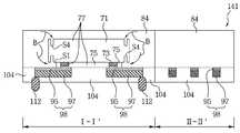
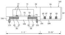
실시예들에 따르는 반도체 하우징 패키지는 몰드막, 하우징 칩, 재배선 패턴 및 하우징 단자를 포함할 수 있다. 상기 하우징 칩은 상기 몰드막에 위치해서 상기 몰드막의 선택된 면으로부터 노출될 수 있다. 상기 재배선 패턴은 상기 하우징 칩으로부터 상기 몰드막의 상기 선택된 면을 향해서 연장할 수 있다. 상기 재배선 패턴은 상기 하우징 칩과 전기적으로 접속할 수 있다. 상기 하우징 단자는 상기 재배선 패턴과 접촉하면서 상기 재배선 패턴으로부터 돌출할 수 있다.The semiconductor housing package according to embodiments may include a mold film, a housing chip, a rewiring pattern, and a housing terminal. The housing chip may be located in the mold film and exposed from a selected side of the mold film. And the rewiring pattern may extend from the housing chip toward the selected face of the mold film. The rewiring pattern may be electrically connected to the housing chip. The housing terminal may protrude from the rewiring pattern while being in contact with the rewiring pattern.
선택된 실시예들에 따라서, 상기 몰드막의 선택된 면은 상기 하우징 칩의 주변에서 편평하거나 굴곡을 가질 수 있다.According to selected embodiments, the selected face of the mold film may be flat or curved around the periphery of the housing chip.
선택된 실시예들에 따라서, 상기 반도체 하우징 패키지는 상기 하우징 칩 아래에 보조 하우징 칩을 적어도 하나 더 포함할 수 있다. 상기 보조 하우징 칩은 접속 볼(Connection ball) 및 리드 선(Lead line) 중 하나를 통해서 상기 재배선 패턴과 전기적으로 접속할 수 있다. 상기 접속 볼은 상기 보조 하우징 칩 및 상기 재배선 패턴 사이에 위치하면서 상기 보조 하우징 칩 및 상기 재배선 패턴과 접촉할 수 있다. 상기 리드 선은 상기 보조 하우징 칩의 주변에 위치해서 상기 보조 하우징 칩 및 상기 재배선 패턴과 접촉할 수 있다.According to selected embodiments, the semiconductor housing package may further include at least one auxiliary housing chip below the housing chip. The auxiliary housing chip may be electrically connected to the rewiring pattern through one of a connection ball and a lead line. The connection ball may be in contact with the auxiliary housing chip and the rewiring pattern while being positioned between the auxiliary housing chip and the rewiring pattern. The lead wire may be located around the auxiliary housing chip and may contact the auxiliary housing chip and the rewiring pattern.
선택된 실시예들에 따라서, 상기 하우징 칩은 제 1 및 2 하우징 칩들을 적어도 포함할 수 있다. 상기 제 1 하우징 칩은 관통 실리콘 비아(Through silicon via; TSV) 및 범프(Bump)를 통해서 상기 제 2 하우징 칩 및 상기 재배선 패턴과 전기적으로 접속할 수 있다. 상기 관통 실리콘 비아는 상기 제 1 하우징 칩을 관통해서 상기 범프 및 상기 재배선 패턴과 접촉할 수 있다. 상기 범프는 상기 관통 실리콘 비아 상에 위치해서 상기 제 2 하우징 칩과 전기적으로 접속할 수 있다.According to selected embodiments, the housing chip may include at least first and second housing chips. The first housing chip may be electrically connected to the second housing chip and the rewiring pattern through a through silicon via (TSV) and a bump. The through silicon vias may contact the bump and the rewiring pattern through the first housing chip. The bumps may be positioned on the through silicon vias and electrically connected to the second housing chip.
선택된 실시예들에 따라서, 상기 하우징 칩은 제 1 및 2 하우징 칩들을 적어도 포함할 수 있다. 상기 제 1 하우징 칩은 관통 실리콘 비아 및 리드 선을 통해서 상기 제 2 하우징 칩 및 상기 재배선 패턴과 전기적으로 접속할 수 있다. 상기 관통 실리콘 비아는 상기 제 1 하우징 칩을 관통해서 상기 리드 선 및 상기 재배선 패턴과 접촉할 수 있다. 상기 리드 선은 상기 관통 실리콘 비아로부터 상기 제 2 하우징 칩으로 연장해서 상기 제 2 하우징 칩과 전기적으로 접속할 수 있다.According to selected embodiments, the housing chip may include at least first and second housing chips. The first housing chip may be electrically connected to the second housing chip and the rewiring pattern through the through silicon vias and the lead wires. The through silicon vias may be in contact with the lead wires and the rewiring pattern through the first housing chip. The lead wire may extend from the through silicon vias to the second housing chip to be electrically connected to the second housing chip.
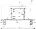
실시예들에 따르는 반도체 패키지 구조물은 반도체 하우징 패키지를 포함할 수 있다. 상기 반도체 하우징 패키지는 몰드막, 상기 몰드막으로 감싸이면서 상기 몰드막으로부터 노출되는 하우징 칩, 상기 몰드막으로부터 상기 하우징 칩을 향하여 연장하면서 상기 하우징 칩과 전기적으로 접속하는 재배선 패턴들, 및 상기 재배선 패턴들로부터 각각 돌출하는 하우징 단자들로 이루어질 수 있다.The semiconductor package structure according to embodiments may include a semiconductor housing package. The semiconductor housing package includes a mold film, a housing chip which is surrounded by the mold film and exposed from the mold film, rewiring patterns extending from the mold film toward the housing chip and electrically connected to the housing chip, And protruding from the line patterns.
실시예들에 따르는 반도체 패키지 구조물은 반도체 베이스 패키지를 더 포함할 수 있다. 상기 반도체 베이스 패키지는 상기 하우징 단자들과 전기적으로 접속하는 회로 기판(Circuit substrate), 및 상기 회로 기판 상에서 상기 하우징 단자들 사이에 위치하면서 상기 회로 기판과 전기적으로 접속하는 베이스 칩(Base chip)으로 이루어질 수 있다The semiconductor package structure according to embodiments may further include a semiconductor base package. The semiconductor base package includes a circuit substrate electrically connected to the housing terminals, and a base chip disposed between the housing terminals on the circuit board and electrically connected to the circuit board. Can
선택된 실시예들에 따라서, 상기 반도체 베이스 패키지는 상기 회로 기판에 제 1 랜딩 패드(Landing pad)들 및 제 2 랜딩 패드들을 포함할 수 있다. 상기 제 1 랜딩 패드들 및 상기 제 2 랜딩 패드들은 상기 회로 기판과 전기적으로 접속할 수 있다. 상기 제 1 랜딩 패드들은 상기 회로 기판의 가장 자리에 배치될 수 있다. 상기 제 2 랜딩 패드들은 상기 회로 기판의 상기 가장 자리 및 중앙 영역 사이에 배치될 수 있다.According to selected embodiments, the semiconductor base package may include first landing pads and second landing pads on the circuit board. The first landing pads and the second landing pads may be electrically connected to the circuit board. The first landing pads may be disposed at the edge of the circuit board. The second landing pads may be disposed between the edge and the central region of the circuit board.
선택된 실시예들에 따라서, 상기 몰드막이 상기 하우징 칩의 주변에서 편평한 형상(Flat shape)을 가지는 경우에, 상기 베이스 칩은 상기 하우징 칩의 두께 방향을 따라서 상기 하우징 단자들의 두께에 한정되어서 상기 회로 기판 상에 배치될 수 있다. 상기 베이스 칩의 두께는 상기 하우징 칩의 상기 두께 방향을 따라서 상기 하우징 단자들의 각각의 두께 대비 작은 크기를 가질 수 있다. 상기 제 1 랜딩 패드들은 상기 하우징 단자들에 접촉될 수 있다. 상기 제 2 랜딩 패드들은 접속 볼들을 통해서 상기 베이스 칩에 전기적으로 접속될 수 있다.According to the selected embodiments, when the mold film has a flat shape in the periphery of the housing chip, the base chip is limited to the thickness of the housing terminals along the thickness direction of the housing chip, Lt; / RTI > The thickness of the base chip may be smaller than the thickness of each of the housing terminals along the thickness direction of the housing chip. The first landing pads may be in contact with the housing terminals. The second landing pads may be electrically connected to the base chip via connection balls.
선택된 실시예들에 따라서, 상기 몰드막이 상기 하우징 칩의 주변에서 요부 형상(Concave shape)을 가지는 경우에, 상기 하우징 단자들은 상기 몰드막 내 상기 요부 형상의 측부들의 끝 단들 상에 위치할 수 있다. 상기 하우징 단자들의 각각은 상기 하우징 칩의 두께 방향을 따라서 상기 베이스 칩과 실질적으로 동일한 크기이거나 다른 크기의 두께를 가질 수 있다. 상기 베이스 칩은 차례로 적층되는 제 1 및 2 베이스 칩들로 적어도 이루어질 수 있다.According to selected embodiments, when the mold film has a concave shape in the periphery of the housing chip, the housing terminals may be located on the ends of the recessed side portions in the mold film. Each of the housing terminals may have substantially the same size or thickness as the base chip along the thickness direction of the housing chip. The base chip may be at least composed of first and second base chips which are stacked one after the other.
상기 제 1 및 2 베이스 칩들은 상기 하우징 칩의 상기 두께 방향을 따라서 상기 요부 형상의 상기 측부들의 길이 및 상기 하우징 단자들의 두께에 한정되어서 상기 하우징 단자들 사이에 배치될 수 있다. 상기 제 1 랜딩 패드들은 상기 하우징 단자들에 접촉될 수 있다. 상기 제 2 랜딩 패드들은 접속 볼들을 통해서 상기 제 1 베이스 칩에 전기적으로 접속될 수 있다. 상기 제 2 베이스 칩은 리드 선들을 통해서 상기 제 1 랜딩 패드들과 전기적으로 접속할 수 있다.The first and second base chips may be disposed between the housing terminals in a manner limited to the length of the recessed side portions and the thickness of the housing terminals along the thickness direction of the housing chip. The first landing pads may be in contact with the housing terminals. The second landing pads may be electrically connected to the first base chip through connection balls. The second base chip may be electrically connected to the first landing pads through lead lines.
선택된 실시예들에 따라서, 상기 몰드막이 상기 하우징 칩의 주변에서 요부 형상을 가지는 경우에, 상기 하우징 단자들은 상기 요부 형상의 측부들의 끝 단들 상에 위치할 수 있다. 상기 하우징 단자들의 각각은 상기 재배선 패턴들의 두께 방향을 따라서 상기 재배선 패턴들의 각각과 실질적으로 동일한 크기의 두께를 가질 수 있다. 상기 베이스 칩은 차례로 적층되는 제 1 및 2 베이스 칩들로 적어도 이루어질 수 있다.According to selected embodiments, when the mold film has a recessed shape in the periphery of the housing chip, the housing terminals may be located on the ends of the recessed side portions. Each of the housing terminals may have a thickness substantially the same as each of the rewiring patterns along the thickness direction of the rewiring patterns. The base chip may be at least composed of first and second base chips which are stacked one after the other.
상기 제 1 및 2 베이스 칩들은 상기 하우징 칩의 두께 방향을 따라서 상기 요부 형상의 상기 측부들의 길이 및 상기 하우징 단자들의 두께에 한정되어서 상기 하우징 단자들 사이에 배치될 수 있다. 상기 제 1 랜딩 패드들은 상기 하우징 단자들에 접촉될 수 있다. 상기 제 2 랜딩 패드들은 접속 볼들을 통해서 상기 제 1 베이스 칩에 전기적으로 접속될 수 있다. 상기 제 2 베이스 칩은 리드 선들을 통해서 상기 제 1 랜딩 패드들과 전기적으로 접속할 수 있다.The first and second base chips may be disposed between the housing terminals in a manner limited to the length of the recessed side portions and the thickness of the housing terminals along the thickness direction of the housing chip. The first landing pads may be in contact with the housing terminals. The second landing pads may be electrically connected to the first base chip through connection balls. The second base chip may be electrically connected to the first landing pads through lead lines.
선택된 실시예들에 따라서, 상기 반도체 패키지 구조물은 상기 하우징 칩 아래에 보조 하우징 칩을 적어도 하나 더 포함할 수 있다. 상기 보조 하우징 칩은 접속 볼들 및 리드 선들 중 선택된 하나의 그룹을 통해서 상기 재배선 패턴들과 전기적으로 접속할 수 있다. 상기 접속 볼들은 상기 보조 하우징 칩 및 상기 재배선 패턴들 사이에 위치하면서 상기 보조 하우징 칩 및 상기 재배선 패턴들과 접촉할 수 있다. 상기 리드 선들은 상기 보조 하우징 칩의 주변에 위치해서 상기 보조 하우징 칩 및 상기 재배선 패턴들과 접촉할 수 있다.According to selected embodiments, the semiconductor package structure may further include at least one auxiliary housing chip below the housing chip. The auxiliary housing chip may be electrically connected to the rewiring patterns through a selected one of the connection balls and the lead wires. The connection balls may be in contact with the auxiliary housing chip and the rewiring patterns while being positioned between the auxiliary housing chip and the rewiring patterns. The lead wires may be located around the auxiliary housing chip and may contact the auxiliary housing chip and the rewiring patterns.
선택된 실시예들에 따라서, 상기 하우징 칩은 제 1 및 2 하우징 칩들을 적어도 포함할 수 있다. 상기 제 1 하우징 칩은 관통 실리콘 비아들 및 범프들을 통해서 상기 제 2 하우징 칩 및 상기 재배선 패턴들과 전기적으로 접속할 수 있다. 상기 관통 실리콘 비아들은 상기 제 1 하우징 칩을 관통해서 상기 범프들 및 상기 재배선 패턴들과 접촉할 수 있다. 상기 범프들은 상기 관통 실리콘 비아들 상에 위치해서 상기 제 2 하우징 칩과 전기적으로 접속할 수 있다.According to selected embodiments, the housing chip may include at least first and second housing chips. The first housing chip may be electrically connected to the second housing chip and the redistribution patterns through the through silicon vias and bumps. The through silicon vias may contact the bumps and the rewiring patterns through the first housing chip. The bumps may be positioned on the through silicon vias and electrically connected to the second housing chip.
선택된 실시예들에 따라서, 상기 하우징 칩은 제 1 및 2 하우징 칩들을 적어도 포함할 수 있다. 상기 제 1 하우징 칩은 관통 실리콘 비아들 및 리드 선들을 통해서 상기 제 2 하우징 칩 및 상기 재배선 패턴들과 전기적으로 접속할 수 있다. 상기 관통 실리콘 비아들은 상기 제 1 하우징 칩을 관통해서 상기 리드 선들 및 상기 재배선 패턴들과 접촉할 수 있다. 상기 리드 선들은 상기 관통 실리콘 비아들로부터 상기 제 2 하우징 칩으로 연장해서 상기 제 2 하우징 칩과 전기적으로 접속할 수 있다.According to selected embodiments, the housing chip may include at least first and second housing chips. The first housing chip may be electrically connected to the second housing chip and the rewiring patterns through the through silicon vias and the lead wires. The through silicon vias may contact the lead wires and the rewiring patterns through the first housing chip. The lead wires extend from the through silicon vias to the second housing chip and are electrically connected to the second housing chip.
선택된 실시예들에 따라서, 상기 재배선 패턴들은 상기 몰드막의 내부 및 상면 중 하나에 배치될 수 있다.According to selected embodiments, the rewiring patterns may be disposed on one of the inner and the upper surface of the mold film.
선택된 실시예들에 따라서, 상기 하우징 칩은 상기 재배선 패턴들의 주변에 칩 바디를 한정하기 위해서 수평면 및 상기 수평면에 수직하는 측벽을 가질 수 있다. 더불어서, 상기 하우징 칩은 상기 수평면 및 상기 측벽을 직접적으로 접촉시킨 모서리, 상기 수평면 및 상기 측벽 사이에 위치하는 경사 면, 상기 수평면 및 상기 측벽 사이에 위치하는 계단 면, 그리고 상기 수평면에 위치하는 요부 중 선택된 하나의 형상을 가질 수 있다.According to selected embodiments, the housing chip may have a horizontal surface and sidewalls perpendicular to the horizontal surface to define the chip body around the rewiring patterns. In addition, the housing chip may include an edge directly contacting the horizontal surface and the sidewall, a sloped surface positioned between the horizontal surface and the sidewall, a stepped surface positioned between the horizontal surface and the sidewall, It can have one selected shape.
상기 몰딩막은 상기 칩 바디에서 상기 모서리 및 상기 측벽과 적어도 접촉하거나 상기 칩 바디에서 상기 수평면, 상기 측벽 및 상기 선택된 하나의 형상과 적어도 접촉할 수 있다.The molding film may be at least in contact with the edge and the sidewall in the chip body or at least with the horizontal surface, the sidewall and the selected one shape in the chip body.
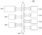
실시예들에 따르는 프로세서 베이스드 시스템은 시스템 보드, 제 1 모듈 장치 및 제 2 모듈 장치를 포함할 수 있다. 시스템 보드는 적어도 하나의 버스 라인(Bus line)을 가질 수 있다. 상기 제 1 모듈 장치는 상기 시스템 보드 상에 위치해서 상기 적어도 하나의 버스 라인과 전기적으로 접속할 수 있다. 상기 제 2 모듈 장치는 상기 시스템 보드 상에 위치해서 상기 적어도 하나의 버스 라인과 전기적으로 접속할 수 있다. 상기 제 1 및 2 모듈 장치들 중 적어도 하나는 반도체 패키지 구조물을 가질 수 있다.A processor-based system according to embodiments may include a system board, a first module device, and a second module device. The system board may have at least one bus line. The first module device may be located on the system board and electrically connect to the at least one bus line. The second module device may be located on the system board and electrically connect to the at least one bus line. At least one of the first and second module devices may have a semiconductor package structure.
상기 반도체 패키지 구조물은 반도체 하우징 패키지 및 반도체 베이스 패키지를 포함할 수 있다. 상기 반도체 하우징 패키지는 몰드막, 상기 몰드막으로 감싸이면서 상기 몰드막으로부터 노출되는 하우징 칩, 상기 몰드막으로부터 상기 하우징 칩을 향하여 연장하면서 상기 하우징 칩과 전기적으로 접속하는 재배선 패턴들, 및 상기 재배선 패턴들로부터 각각 돌출하는 하우징 단자들로 이루어질 수 있다.The semiconductor package structure may include a semiconductor housing package and a semiconductor base package. The semiconductor housing package includes a mold film, a housing chip which is surrounded by the mold film and exposed from the mold film, rewiring patterns extending from the mold film toward the housing chip and electrically connected to the housing chip, And protruding from the line patterns.
상기 반도체 베이스 패키지는 상기 하우징 단자들과 전기적으로 접속하는 회로 기판, 및 상기 회로 기판 상에서 상기 하우징 단자들 사이에 위치하면서 상기 회로 기판과 전기적으로 접속하는 베이스 칩으로 이루어질 수 있다.The semiconductor base package may include a circuit board electrically connected to the housing terminals, and a base chip disposed between the housing terminals on the circuit board and electrically connected to the circuit board.
선택된 실시예들에 따라서, 상기 제 1 모듈 장치는 중앙 처리 장치(Central Processing Unit), 플로피 디스크 드라이브(Floppy Disk Drive) 및 콤팩 디스크 롬 드라이브(Compack Disk ROM Drive)를 포함할 수 있다.According to selected embodiments, the first module device may include a central processing unit, a floppy disk drive, and a compact disk ROM drive.
상기 제 2 모듈 장치는 제 1 입/ 출력 장치(First I/O Device), 제 2 입/ 출력 장치(Second I/O Device), 롬(Read-only Memory) 및 램(Random Access Memory)을 포함할 수 있다.The second module device includes a first I / O device, a second I / O device, a read-only memory, and a random access memory can do.
선택된 실시예들에 따라서, 상기 몰드막은 상기 하우징 칩의 주변에서 편평한 형상 및 요부 형상 중 하나를 가질 수 있다.According to selected embodiments, the mold film may have one of a flat shape and a recessed shape in the periphery of the housing chip.
선택된 실시예들에 따라서, 상기 프로세서 베이스드 시스템은 상기 하우징 칩 아래에 보조 하우징 칩을 적어도 하나 더 포함할 수 있다. 상기 보조 하우징 칩은 접속 볼들 및 리드 선들 중 선택된 하나의 그룹을 통해서 상기 재배선 패턴들과 전기적으로 접속할 수 있다. 상기 접속 볼들은 상기 보조 하우징 칩 및 상기 재배선 패턴들 사이에 위치하면서 상기 보조 하우징 칩 및 상기 재배선 패턴들과 접촉할 수 있다. 상기 리드 선들은 상기 보조 하우징 칩의 주변에 위치해서 상기 보조 하우징 칩 및 상기 재배선 패턴들과 접촉할 수 있다.According to selected embodiments, the processor-based system may further include at least one auxiliary housing chip below the housing chip. The auxiliary housing chip may be electrically connected to the rewiring patterns through a selected one of the connection balls and the lead wires. The connection balls may be in contact with the auxiliary housing chip and the rewiring patterns while being positioned between the auxiliary housing chip and the rewiring patterns. The lead wires may be located around the auxiliary housing chip and may contact the auxiliary housing chip and the rewiring patterns.
선택된 실시예들에 따라서, 상기 하우징 칩은 제 1 및 2 하우징 칩들을 적어도 포함할 수 있다. 상기 제 1 하우징 칩은 관통 실리콘 비아들 및 범프들을 통해서 상기 제 2 하우징 칩 및 상기 재배선 패턴들과 전기적으로 접속할 수 있다. 상기 관통 실리콘 비아들은 상기 제 1 하우징 칩을 관통해서 상기 범프들 및 상기 재배선 패턴들과 접촉할 수 있다. 상기 범프들은 상기 관통 실리콘 비아들 상에 위치해서 상기 제 2 하우징 칩과 전기적으로 접속할 수 있다.According to selected embodiments, the housing chip may include at least first and second housing chips. The first housing chip may be electrically connected to the second housing chip and the redistribution patterns through the through silicon vias and bumps. The through silicon vias may contact the bumps and the rewiring patterns through the first housing chip. The bumps may be positioned on the through silicon vias and electrically connected to the second housing chip.
상술한 바와 같이, 실시예들은 종래 기술과 다르게 인쇄 회로 기판을 사용하지 않으면서 하우징 칩을 외부와 전기적으로 접속시킬 수 있는 반도체 하우징 패키지를 제공할 수 있다. 이를 위해서, 상기 하우징 칩은 반도체 하우징 패키지에서 몰드막 및 재배선 패턴들로 둘러싸일 수 있다. 상기 몰드막은 에폭시 몰딩 컴파운드일 수 있다. 상기 재배선 패턴들은 도전 물질일 수 있다.As described above, the embodiments can provide a semiconductor housing package that can electrically connect the housing chip to the outside without using a printed circuit board unlike the prior art. To this end, the housing chip may be surrounded by a mold film and rewiring patterns in a semiconductor housing package. The mold film may be an epoxy molding compound. The rewiring patterns may be a conductive material.
실시예들은 인쇄 회로 기판을 사용하는 반도체 베이스 패키지, 및 인쇄 회로 기판을 사용하지 않는 반도체 하우징 패키지를 포함하는 반도체 구조물을 제공할 수 있다. 상기 반도체 하우징 패키지는 반도체 베이스 패키지 상에 위치해서 반도체 베이스 패키지와 전기적으로 접속할 수 있다. 상기 반도체 하우징 패키지는 종래 기술 대비 반도체 패키지 구조물의 고집적화를 구현시킬 수 있다.Embodiments may provide a semiconductor structure including a semiconductor base package using a printed circuit board and a semiconductor housing package not using a printed circuit board. The semiconductor housing package is positioned on the semiconductor base package and can be electrically connected to the semiconductor base package. The semiconductor housing package can realize high integration of the semiconductor package structure compared to the prior art.
실시예들은 반도체 베이스 패키지 및 반도체 하우징 패키지로 이루어지는 반도체 패키지 구조물을 포함하는 프로세서 베이스드 시스템을 제공할 수 있다. 상기 반도체 패키지 구조물은 반도체 하우징 패키지를 사용하기 때문에 종래 기술 대비 프로세서 베이스드 시스템의 내부 구조를 단순화시킬 수 있다. 상기 반도체 패키지 구조물은 인쇄 회로 기판의 사용 횟수를 최소화시키기 때문에 종래 기술 대비 프로세서 베이스드 시스템의 제조 단가를 낮출 수 있다.Embodiments may provide a processor-based system that includes a semiconductor package structure comprising a semiconductor base package and a semiconductor housing package. Since the semiconductor package structure uses a semiconductor housing package, it is possible to simplify the internal structure of the processor-based system compared to the prior art. Because the semiconductor package structure minimizes the number of times of use of the printed circuit board, the manufacturing cost of the processor-based system can be reduced compared to the prior art.
도 1 은 실시예들에 따르는 반도체 패키지 구조물들을 보여주는 평면도이다.
도 2 는 도 1 의 절단선 Ⅰ-Ⅰ' 를 따라 취해서 도 1 의 반도체 패키지 구조물들 중 선택된 하나를 보여주는 단면도이다.
도 3 내지 5 는 도 1 의 절단선들 Ⅰ-Ⅰ' 및 Ⅱ-Ⅱ' 를 따라 취해서 실시예들에 따르는 반도체 패키지 구조물의 반도체 하우징 패키지의 형성방법을 설명하는 단면도들이다.
도 6 내지 9 는 도 1 의 절단선들 Ⅰ-Ⅰ' 및 Ⅱ-Ⅱ' 를 따라 취해서 실시예들에 따르는 반도체 패키지 구조물의 반도체 하우징 패키지의 형성방법을 설명하는 단면도들이다.
도 10 및 11 은 도 1 의 절단선들 Ⅰ-Ⅰ' 및 Ⅱ-Ⅱ' 를 따라 취해서 실시예들에 따르는 반도체 패키지 구조물의 반도체 하우징 패키지의 형성방법을 설명하는 단면도들이다.
도 12 내지 14 는 도 1 의 절단선들 Ⅰ-Ⅰ' 및 Ⅱ-Ⅱ' 를 따라 취해서 실시예들에 따르는 반도체 패키지 구조물의 반도체 하우징 패키지의 형성방법을 설명하는 단면도들이다.
도 15 는 도 1 의 절단선들 Ⅰ-Ⅰ' 를 따라 취해서 실시예들에 따르는 반도체 패키지 구조물의 반도체 하우징 패키지의 형성방법을 보여주는 단면도이다.
도 16 은 도 1 의 절단선들 Ⅰ-Ⅰ' 를 따라 취해서 실시예들에 따르는 반도체 패키지 구조물의 반도체 하우징 패키지의 형성방법을 보여주는 단면도이다.
도 17 은 도 1 의 절단선들 Ⅰ-Ⅰ' 를 따라 취해서 실시예들에 따르는 반도체 패키지 구조물의 형성방법을 보여주는 단면도이다.
도 18 은 도 1 의 절단선들 Ⅰ-Ⅰ' 를 따라 취해서 실시예들에 따르는 반도체 패키지 구조물의 형성방법을 보여주는 단면도이다.
도 19 는 도 1 의 절단선들 Ⅰ-Ⅰ' 를 따라 취해서 실시예들에 따르는 반도체 패키지 구조물의 반도체 하우징 패키지의 형성방법을 보여주는 단면도이다.
도 20 은 도 1 의 절단선들 Ⅰ-Ⅰ' 를 따라 취해서 실시예들에 따르는 반도체 패키지 구조물의 반도체 하우징 패키지의 형성방법을 보여주는 단면도이다.
도 21 은 도 1 의 반도체 패키지 구조물들 중 적어도 하나를 포함하는 프로세서 베이스드 시스템을 보여주는 평면도이다.1 is a plan view showing semiconductor package structures according to embodiments.
FIG. 2 is a cross-sectional view taken along section line I-I 'of FIG. 1 showing a selected one of the semiconductor package structures of FIG.
FIGS. 3 to 5 are cross-sectional views illustrating a method of forming a semiconductor housing package of a semiconductor package structure according to embodiments, taken along the cutting lines I-I 'and II-II' of FIG.
6 to 9 are cross-sectional views illustrating a method of forming a semiconductor housing package of a semiconductor package structure according to embodiments taken along the cutting lines I-I 'and II-II' of FIG.
FIGS. 10 and 11 are cross-sectional views illustrating a method of forming a semiconductor housing package of a semiconductor package structure according to embodiments, taken along the cutting lines I-I 'and II-II' of FIG.
12 to 14 are cross-sectional views illustrating a method of forming a semiconductor housing package of a semiconductor package structure according to embodiments taken along the cutting lines I-I 'and II-II' of FIG.
15 is a cross-sectional view taken along section lines I-I 'of FIG. 1 to illustrate a method of forming a semiconductor housing package of a semiconductor package structure according to embodiments.
FIG. 16 is a cross-sectional view taken along section lines I-I 'of FIG. 1 to illustrate a method of forming a semiconductor housing package of a semiconductor package structure according to embodiments.
FIG. 17 is a cross-sectional view taken along the cutting lines I-I 'of FIG. 1 to illustrate a method of forming a semiconductor package structure according to embodiments.
FIG. 18 is a cross-sectional view taken along the cutting lines I-I 'of FIG. 1 to illustrate a method of forming a semiconductor package structure according to embodiments.
FIG. 19 is a cross-sectional view taken along section lines I-I 'of FIG. 1 to illustrate a method of forming a semiconductor housing package of a semiconductor package structure according to embodiments.
FIG. 20 is a cross-sectional view taken along section lines I-I 'of FIG. 1 illustrating a method of forming a semiconductor housing package of a semiconductor package structure according to embodiments.
21 is a plan view showing a processor-based system including at least one of the semiconductor package structures of FIG.
상기 실시예들은 이후로 첨부 도면들을 참조해서 설명하기로 한다. 그러나, 상기 양태는 여러 가지 다른 형태들로 구체화되어질 수 있고, 그리고 여기에서 설명되는 양태로 한정되는 것으로 해석되지 않는다. 오히려, 상기 양태는 실시예들을 더욱 철저하고 그리고 완전하게 되도록 해주며, 당업자에게 실시예들의 영역을 충분히 전달할 수 있도록 해준다. 비록 제 1, 제 2, 보조 .. 등을 지칭하는 용어들이 여러 구성 요소들을 기술하기 위하여 여기에서 사용되어질 수 있다면, 상기 구성 요소들은 이러한 용어들로 한정되지 않는 것으로 이해되어 질 것이다. 단지, 이러한 용어들은 어떤 구성 요소로부터 다른 구성 요소를 구별하기 위해서 사용되어 질 뿐이다.The embodiments will be described below with reference to the accompanying drawings. However, the embodiments may be embodied in many different forms and are not to be construed as limited to the embodiments described herein. Rather, the foregoing aspects will make the embodiments more thorough and complete, and will enable those skilled in the art to fully convey the scope of the embodiments. It will be understood that, although the terms referring to first, second, auxiliary, etc. may be used herein to describe various components, the components are not intended to be limited to these terms. However, these terms are only used to distinguish different components from one component.
여기에서, 사용되어 진 바와 같이, 구성 요소들의 물질의 종류는 반도체 패키지 구조물을 접하는 당업자에게 많이 공지되어 있기 때문에 도전 물질 및 절연 물질로만 구분하기로 한다. '적어도 하나' 를 지칭하는 용어는 하나 이상으로 관련을 가지고 열거된 항목들에 대해서 유추할 수 있는 모든 조합들을 포함한다. 더불어서, '사이에, 아래에, 주변에 및 상에' 등과 같이 특별히 상대적인 용어들은 선택된 구성 요소, 다른 구성 요소와 어떤 형상과의 상대적인 관계, 또는 도면들에 도시된 형상을 간단하게 설명하는데 설명의 간소화를 위해서 사용되어 질 수 있다. 그리고, 여기에서 전문용어의 사용은 특별한 양태를 단지 설명하기 위함이지 실시예들을 한정하려는 것은 아니다.Here, as used, the types of materials of the components are classified as conductive materials and insulating materials only because they are well known to those skilled in the art of contacting semiconductor package structures. The term " at least one " includes all combinations that can be inferred relative to one or more of the listed items. In addition, specific terms relative to each other, such as "between, under, around and on", etc., will be used to simply describe the selected component, its relative relationship with other components, Can be used for simplification. And the use of terminology herein is for the purpose of describing particular embodiments only and is not intended to limit the embodiments.
이제, 실시예들에 따르는 반도체 패키지 구조물은 도 1 및 도 2 를 참조해서 보다 상세하게 설명하기로 한다.Now, the semiconductor package structure according to the embodiments will be described in more detail with reference to FIGS. 1 and 2. FIG.
도 1 은 실시예들에 따르는 반도체 패키지 구조물들을 보여주는 평면도이다.1 is a plan view showing semiconductor package structures according to embodiments.
도 1 을 참조하면, 반도체 패키지 구조물(183, 186 또는 189)은 반도체 하우징 패키지(Semiconductor housing package; 141, 143, 145, 147, 149, 174 또는 178)를 포함할 수 있다. 상기 반도체 하우징 패키지(141, 143, 145, 147, 149, 174 또는 178)는 도 1 에서 실선으로 표시할 수 있다. 이 경우에, 상기 반도체 하우징 패키지(141, 143, 145, 147, 149, 174 또는 178)는 하우징 칩(Housing chip; 77) 및 몰드막(Mold layer; 84 또는 88)을 가질 수 있다.Referring to FIG. 1, the
상기 하우징 칩(77)은 접속 패드(Connection pad; 73)들을 가질 수 있다. 상기 접속 패드(73)들은 하우징 칩(77)의 가장 자리 및/ 또는 다른 영역에 배치될 수 있다. 상기 하우징 칩(77)은 몰드막(84 또는 88)의 중앙 영역에 배치될 수 있다. 상기 몰드막(84 또는 88)은 하우징 칩(77)의 주변에 위치해서 하우징 칩(77)을 둘러쌀 수 있다. 상기 몰드막(84 또는 88)은 인쇄 회로 기판(PCB)의 대체물일 수 있다.The
상기 반도체 하우징 패키지(141, 143, 145, 147, 149, 174 또는 178)는 재배선 패턴(Reinterconnection pattern; 98 또는 99)들 및 하우징 단자(Housing node; 112, 114, 116 또는 118)들을 더 가질 수 있다. 상기 재배선 패턴(98 또는 99)들은 하우징 칩(77) 내 접속 패드(73)들로부터 몰드막(84 또는 88) 내 하우징 단자(112, 114, 116 또는 118)들을 향해서 연장할 수 있다. 상기 재배선 패턴(98 또는 99)들은 접속 단자(73)들 및 하우징 단자(112, 114, 116 또는 118)들과 접촉할 수 있다. 상기 재배선 패턴(98 또는 99)들은 도 1 과 다른 형상을 가질 수도 있다.The
상기 하우징 단자(112, 114, 116 또는 118)들은 하우징 칩(77)으로부터 이격해서 몰드막(84 또는 88) 내 위치할 수 있다. 상기 하우징 단자(112, 114, 116 또는 118)들은 재배선 패턴(98 또는 98)들을 통해서 접속 단자(73)들과 일대일로 대응하거나 대응하지 않을 수 있다. 따라서, 상기 하우징 단자(112, 114, 116 또는 118)들은 접속 단자(73)들과 동일한 개수이거나 다른 개수일 수 있다. 한편, 상기 반도체 패키지 구조물(183, 186 또는 189)은 반도체 베이스 패키지(Semiconductor base package; 54 또는 58)를 포함할 수 있다.The
상기 반도체 베이스 패키지(54 또는 58)는 도 1 에서 점선으로 표시할 수 있다. 상기 반도체 베이스 패키지(54 또는 58)는 회로 기판(Circuit substrate; 3) 및 베이스 칩(Base chip; 24, 또는 24 및 28)을 가질 수 있다. 상기 회로 기판(3)은 반도체 하우징 패키지(141, 143, 145, 147, 149, 174 또는 178)의 몰드막(84 또는 88)과 정렬해서 중첩할 수 있다. 상기 회로 기판(3)은 인쇄 회로 기판(PCB)일 수 있다. 상기 회로 기판(3)은 기판 단자(Substrate node; 9)들을 가질 수 있다. 상기 기판 단자(9)들은 회로 기판(3)의 가장 자리에 위치할 수 있다.The
상기 기판 단자(9)들은 회로 기판(3)의 가장 자리 및/ 또는 다른 영역에 위치할 수 있다. 상기 기판 단자(9)들은 반도체 하우징 패키지(141, 143, 145, 147, 149, 174 또는 178)의 하우징 단자(112, 114, 116 또는 118)들과 정렬해서 중첩할 수 있다. 상기 기판 단자(9)들은 하우징 단자(112, 114, 116 또는 118)들과 정렬하지 않을 수도 있다. 상기 기판 단자(9)들은 하우징 단자(112, 114, 116 또는 118)들과 동일한 개수이거나 다른 개수일 수 있다. 상기 베이스 칩(24)은 회로 기판(3)의 중앙 영역에 배치될 수 있다.The
상기 베이스 칩(24)은 반도체 하우징 패키지(141, 143, 145, 147, 149, 174 또는 178)의 하우징 칩(77)과 정렬해서 중첩할 수 있다. 상기 베이스 칩(24)은 반도체 하우징 패키지(141, 143, 145, 147, 149, 174 또는 178)의 하우징 칩(77)과 중첩하지 않을 수도 있다. 상기 베이스 칩(24)은 접속 볼(14)들을 통해서 회로 기판(3)과 전기적으로 접속할 수 있다. 상기 접속 볼(Connection ball; 14)들은 하우징 칩(77)의 접속 단자(73)들과 정렬해서 중첩할 수 있다. 상기 접속 볼(14)들은 하우징 칩(77)의 접속 단자(73)들과 중첩하지 않을 수도 있다.The
도 2 는 도 1 의 절단선 Ⅰ-Ⅰ' 를 따라 취해서 도 1 의 반도체 패키지 구조물들 중 선택된 하나를 보여주는 단면도이다.FIG. 2 is a cross-sectional view taken along section line I-I 'of FIG. 1 showing a selected one of the semiconductor package structures of FIG.
도 2 를 참조하면, 반도체 패키지 구조물(183)은 반도체 하우징 패키지(141)를 포함할 수 있다. 상기 반도체 하우징 패키지(141)는 몰드막(84) 및 하우징 칩(77)을 포함할 수 있다. 상기 몰드막(84)은 하우징 칩(77)을 감싸면서 하우징 칩(77)을 부분적으로 노출시킬 수 있다. 상기 몰드막(84)은 하우징 칩(77)의 주변에서 편평한 형상(Flat shape)을 가질 수 있다. 상기 몰드막(84)은 에폭시 몰딩 컴파운드를 포함할 수 있다.Referring to FIG. 2, the
상기 하우징 칩(77)은 칩 바디(Chip body; 71), 접속 패드(73)들 및 절연막(Insulating layer; 75)을 포함할 수 있다. 상기 칩 바디(71)는 반도체 회로를 가질 수 있다. 상기 칩 바디(71)는 절연막(75)과 실질적으로 평행한 수평면들, 및 상기 수평면들에 대해서 수직한 측벽들로 한정될 수 있다. 상기 반도체 회로는 단독으로 로직(Logic) 회로, 또는 로직 및 메모리(Memory) 회로들을 지칭할 수 있다. 상기 접속 패드(73)들은 칩 바디(71) 상에 위치할 수 있다. 상기 접속 패드(73)들은 칩 바디(71)의 반도체 회로와 전기적으로 접속할 수 있다.The
상기 접속 패드(73)들은 절연막(75) 및 몰드막(84)을 통해서 노출될 수 있다. 상기 접속 패드(73)은 도전 물질을 포함할 수 있다. 상기 절연막(75)은 접속 패드(73)들을 둘러쌀 수 있다. 상기 절연막(75)의 두께는 하우징 칩(77)의 두께 방향으로 접속 패드(73)의 두께와 동일하거나 다를 수 있다. 상기 절연막(75)은 절연 물질을 포함할 수 있다. 상기 하우징 칩(77)은 몰드막(84)과 함께 몰드 구조체(A1)를 구성할 수 있다. 상기 반도체 하우징 패키지(141)는 재배선 패턴(98)들, 보호막(104) 및 하우징 단자(112)들을 더 포함할 수 있다.The
상기 재배선 패턴(98)들은 보호막(104)을 통해서 접속 패드(73)들과 접촉할 수 있다. 상기 재배선 패턴(98)들은 하우징 칩(77)으로부터 몰드막(84)을 향해서 연장할 수 있다. 상기 재배선 패턴(98)들은 도전 물질을 포함할 수 있다. 상기 보호막(104)은 하우징 칩(77), 몰딩막(84) 및 재배선 패턴(98)들 상에 덮인다. 이 경우에, 상기 보호막(104)은 재배선 패턴(98)들을 부분적으로 노출시킬 수 있다. 상기 하우징 단자(112)들은 보호막(104)을 통해서 재배선 패턴(98)들과 접촉할 수 있다.The
상기 하우징 단자(112)들은 보호막(104)으로부터 돌출할 수 있다. 상기 하우징 단자(112)들은 도전 물질을 포함할 수 있다. 한편, 상기 반도체 패키지 구조물(163)은 반도체 베이스 패키지(54)를 더 포함할 수 있다. 상기 반도체 베이스 패키지(54)는 회로 기판(3)을 포함할 수 있다. 상기 회로 기판(3)은 도전 패턴들을 포함할 수 있다. 상기 도전 패턴들은 회로 기판(3)에서 목적하는 회로를 구성할 수 있다.The
상기 회로 기판(3)은 인쇄 회로 기판(PCB)을 포함할 수 있다. 상기 회로 기판(3)은 랜딩 패드(Landing pad; 6)들 및 기판 단자(9)들을 더 포함할 수 있다. 상기 랜딩 패드(6)들은 회로 기판(3)의 도전 패턴들과 전기적으로 접속한다. 상기 랜딩 패드(6)들은 제 1 및 2 랜딩 패드들로 이루어질 수 있다. 상기 제 1 랜딩 패드(6)들은 회로 기판(3)의 가장 자리에 배치될 수 있다. 상기 제 1 랜딩 패드(6)들은 반도체 하우징 패키지(142)의 하우징 단자(112)들에 접촉될 수 있다.The
상기 제 2 랜딩 패드(6)들은 회로 기판(3)의 가장 자리 및 중앙 영역 사이에 배치될 수 있다. 상기 제 1 및 2 랜딩 패드(6)들은 도전 물질을 포함할 수 있다. 상기 기판 단자(9)들은 회로 기판(3) 아래에 위치해서 제 1 랜딩 패드(6)들과 접촉할 수 있다. 상기 반도체 베이스 패키지(54)는 접속 볼(14)들, 베이스 칩(24), 접착제(Adhesive; 35) 및 베이스 충진제(Base filler; 44)를 더 포함할 수 있다. 상기 접속 볼(14)들은 제 2 랜딩 패드(6)들과 접촉할 수 있다. 상기 접속 볼(14)들은 도전 물질을 포함할 수 있다.The
상기 베이스 칩(24)은 반도체 회로를 가질 수 있다. 상기 반도체 회로는 단독으로 로직 회로, 또는 로직 및 메모리 회로들을 지칭할 수 있다. 상기 베이스 칩(24)은 접속 볼(14)들 상에 위치할 수 있다. 상기 베이스 칩(24)은 반도체 회로를 통해서 접속 볼(14)들과 전기적으로 접속할 수 있다. 상기 베이스 칩(24)은 하우징 칩(77)의 두께 방향을 따라서 반도체 하우징 패키지(142)의 하우징 단자(112)들의 두께에 한정되어서 하우징 단자(112)들 사이에 배치될 수 있다.The
이 경우에, 상기 베이스 칩(24)의 두께는 하우징 칩(77)의 두께 방향을 따라서 하우징 단자(112)들의 각각의 두께 대비 작은 크기를 갖는다. 상기 접착제(35)는 베이스 칩(24) 상에 배치될 수 있다. 상기 접착제(35)는 베이스 칩(24)에서 접속 볼(14)들과 대향하는 면 상에 배치될 수 있다. 상기 접착제(35)는 베이스 칩(24)을 반도체 하우징 패키지(142)의 보호막(104) 상에 부착시킬 수 있다. 상기 접착제(35)는 절연 물질을 포함할 수 있다.In this case, the thickness of the
상기 베이스 충진제(44)는 회로 기판(3) 상에 위치해서 베이스 칩(24)을 적어도 덮을 수 있다. 상기 베이스 충진제(44)는 제 1 랜딩 패드(6)들을 노출시키면서 회로 기판(3) 및 베이스 칩(24) 사이를 채울 수 있다. 상기 베이스 충진제(44)는 베이스 칩(24)을 회로 기판(3) 상에 부착시킬 수 있다. 상기 베이스 충진제(44)는 절연 물질을 포함할 수 있다.
The
[제 1 실시예][First Embodiment]
도 3 내지 5 는 도 1 의 절단선들 Ⅰ-Ⅰ' 및 Ⅱ-Ⅱ' 를 따라 취해서 실시예들에 따르는 반도체 패키지 구조물의 반도체 하우징 패키지의 형성방법을 설명하는 단면도들이다. 도 3 내지 5 는 도 2 와 동일한 부재에 대해서 동일한 부호를 사용하기로 한다.FIGS. 3 to 5 are cross-sectional views illustrating a method of forming a semiconductor housing package of a semiconductor package structure according to embodiments, taken along the cutting lines I-I 'and II-II' of FIG. 3 to 5, the same reference numerals are used for the same members as those in Fig.
도 3 을 참조하면, 실시예들에 따라서, 지지대(Supporting plate; 62) 및 하우징 칩(77)을 준비할 수 있다. 상기 지지대(62)는 유연성을 가지는 물질 또는 유연성을 가지지 않는 물질을 포함할 수 있다. 상기 지지대(62) 상에 하우징 칩(77)을 위치시킬 수 있다. 상기 하우징 칩(77)은 칩 바디(71), 접속 패드(73)들 및 절연막(75)을 포함할 수 있다. 상기 칩 바디(71)는 반도체 회로을 가질 수 있다. 상기 반도체 회로는 단결정 실리콘, 절연 물질, 도전 물질 및 불순물 이온들을 포함할 수 있다.Referring to FIG. 3, according to embodiments, a supporting
상기 접속 패드(73)들은 칩 바디(71)의 반도체 회로와 전기적으로 접속할 수 있다. 상기 접속 패드(73)들은 도전 물질을 포함할 수 있다. 상기 절연막(75)은 칩 바디(71) 상에 위치해서 접속 패드(73)들을 노출시킬 수 있다. 상기 절연막(75)은 적어도 하나의 절연물질을 포함할 수 있다. 이 경우에, 상기 절연막(75)은 칩 바디(71) 상에 위치해서 지지대(62)와 접촉할 수 있다. 상기 절연막(75)은 지지대(62) 및 접속 패드(73)들 사이에 빈 공간(Vacant space; 64)들을 가질 수 있다.The
상기 지지대(62), 접속 패드(73)들 및 절연막(75)은 빈 공간(64)들을 한정할 수 있다. 상기 하우징 칩(77)을 감싸도록 지지대(62) 상에 몰드막(84)을 형성할 수 있다. 상기 몰드막(84)은 에폭시 몰딩 컴파운드(Epoxy molding compound)를 포함한다. 상기 몰드막(84)은 하우징 칩(77)과 함께 몰드 구조체(A1)를 구성할 수 있다. 이와는 다르게, 상기 하우징 칩(77) 및 몰드막(84) 상에 지지대(62)를 사용하지 않을 수도 있다.The
이를 위해서, 상기 몰드막(84)은 하우징 칩(77) 대비 성형체(Molding body; 도면에 미 도시)에 먼저 위치될 수도 있다. 상기 성형체는 몰드막(84)을 둘러싸는 외부면을 한정하고, 그리고 몰드막(84)의 외부 면의 소정 영역에 안착부(Mounting portion)를 형성할 수도 있다. 상기 안착부는 몰드막(84)의 외부면으로부터 몰드막(84)의 내부를 향하도록 연장할 수도 있다. 상기 몰딩막(84)의 안착부에 하우징 칩(77)을 위치시킬 수도 있다.For this purpose, the
상기 하우징 칩(77)은 몰딩막(84)을 통해서 접속 패드(73)들 및 절연막(75)을 노출시키도록 몰딩막(84)의 안착부 상에 위치될 수도 있다. 상기 몰딩막(84) 상에 열(Heat)을 적용하거나 적용하지 않을 수 있다. 이 경우에, 상기 몰딩막(84)은 하우징 칩(77)의 접속 패드(73)들 및 절연막(75)을 계속적으로 노출시키도록 하우징 칩(77)을 둘러싸면서 하우징 칩(77)과 접촉할 수도 있다. 이를 통해서, 상기 몰드막(84)은 하우징 칩(77)과 함께 몰드 구조체(A1)를 구성할 수도 있다.The
도 4 를 참조하면, 실시예들에 따라서, 상기 몰드 구조체(A1)로부터 지지대(62)를 분리할 수 있다. 이와는 다르게, 상기 몰드 구조체(A1) 아래에 지지대(62)를 사용하지 않는 경우에, 상기 몰드막(84)으로부터 성형체를 분리시킬 수도 있다. 계속해서, 상기 몰드 구조체(A1) 상에 제 1 도전막(91) 및 제 2 도전막(93)을 차례로 형성할 수 있다. 상기 제 1 도전막(91)은 몰드 구조체(A1) 상에 스퍼터 공정(Sputter process)을 수행해서 형성될 수 있다.Referring to Fig. 4, the
상기 제 1 도전막(91)은 몰드막(84) 및 절연막(75) 상에 위치해서 접속 패드(73)들과 접촉할 수 있다. 상기 제 1 도전막(91)은 몰드막(84) 상에 제 2 도전막(93)의 형성 및/ 또는 몰드 막(84) 상에 제 2 도전막(93)의 부착을 적절하게 도와줄 수 있다. 상기 제 1 도전막(91)은 크롬(Cr)을 포함할 수 있다. 상기 제 2 도전막(93)은 제 1 도전막(91) 상에 전기 도금 공정(Electroplating process)을 통해서 형성될 수 있다. 상기 제 2 도전막(93)은 알루미늄(Al) 또는 구리(Cu)를 포함할 수 있다.The first
도 5 를 참조하면, 실시예들에 따라서, 상기 제 1 및 2 도전막들(91, 93) 상에 포토 및 식각 공정들을 수행해서 제 1 및 2 도전 패턴들(95, 97)을 형성할 수 있다. 상기 제 1 및 2 도전 패턴들(95, 97)은 절연막(75) 및 몰드막(84)을 노출시킬 수 있다. 상기 제 1 및 2 도전 패턴들(95, 97)은 재배선 패턴(98)들을 구성할 수 있다. 상기 재배선 패턴(98)들은 하우징 칩(77)으로부터 몰드막(84)을 향해서 연장할 수 있다.Referring to FIG. 5, photo and etch processes may be performed on the first and second
상기 재배선 패턴(98)들은 접속 패드(73)들을 부분적으로 노출시키거나 접속 패드(73)들을 노출시키지 않을 수 있다. 상기 재배선 패턴(98)들을 덮도록 절연막(75) 및 몰드막(84) 상에 보호막(104)을 형성할 수 있다. 상기 보호막(104)은 스퍼터 공정 또는 증착(Deposition) 공정을 통해서 형성될 수 있다. 상기 보호막(104)은 개구부들을 통해서 재배선 패턴(98)들을 부분적으로 노출시킬 수 있다. 상기 보호막(104)은 절연 물질을 포함할 수 있다.The
상기 보호막(104)에 하우징 단자(112)들을 형성할 수 있다. 상기 하우징 단자(112)들은 솔더링(Soldering) 공정을 통해서 형성될 수 있다. 상기 하우징 단자(112)들은 보호막(104)의 개구부들을 통해서 재배선 패턴(98)들과 접촉할 수 있다. 상기 하우징 단자(112)들은 보호막(104)으로부터 돌출할 수 있다. 상기 하우징 단자(112)들은 도전 물질을 포함할 수 있다. 상기 하우징 단자(112)들은 몰드 구조체(A1), 재배선 패턴(98)들 및 보호막(104)과 함께 반도체 하우징 패키지(141)를 구성할 수 있다.
이와는 다르게, 상기 반도체 하우징 패키지(141)는 잉크젯(inkjet) 방식으로 인쇄된 재배선 패턴(98)들, 보호막(104) 및/ 또는 하우징 단자(112)들을 가질 수도 있다. 상기 잉크젯 방식은 도전성 잉크(Conductive ink) 및/ 또는 절연성 잉크(Insulating ink)를 하우징 칩(77) 및 몰딩막(84) 상에 인쇄하는 것과, 도전성 잉크 및/ 또는 절연성 잉크를 가열하는 것을 포함할 수 있다. 이 경우에, 상기 도전성 잉크는 하우징 칩(77) 및 몰딩막(84) 상에 선택적으로 인쇄되어서 도 5 의 재배선 패턴(98)들 및/ 또는 하우징 단자(112)들을 형성할 수 있다.Alternatively, the
상기 절연성 잉크는 하우징 칩(77), 몰딩막(84) 및 재배선 패턴(98)들 상에 위치해서 보호막(104)을 형성할 수 있다.
The insulating ink may be positioned on the
[제 2 실시예][Second Embodiment]
도 6 내지 9 는 도 1 의 절단선들 Ⅰ-Ⅰ' 및 Ⅱ-Ⅱ' 를 따라 취해서 실시예들에 따르는 반도체 패키지 구조물의 하우징 패키지의 형성방법을 설명하는 단면도들이다. 도 6 내지 9 는 도 3 내지 5 와 동일한 부재에 대해서 동일한 참조 부호를 사용하기로 한다.6 to 9 are cross-sectional views illustrating a method of forming a housing package of a semiconductor package structure according to embodiments taken along the cutting lines I-I 'and II-II' of FIG. 6 to 9, the same reference numerals are used for the same members as those in Figs.
도 6 을 참조하면, 실시예들에 따라서, 도 3 의 지지대(62) 및 하우징 칩(77)을 준비할 수 있다. 상기 하우징 칩(77)은 지지대(62) 상에 위치될 수 있다. 상기 하우징 칩(77) 상에 식각 공정을 수행할 수 있다. 상기 식각 공정은 습식 또는 건식 에천트를 사용해서 지지대(62), 칩 바디(71), 접속 패드(73)들 대비 절연막(75)에 대해서 식각률을 가질 수 있다. 상기 습식 또는 건식 에천트는 절연막(75)을 부분적으로 식각할 수 있다.Referring to FIG. 6, according to embodiments, the
상기 절연막(75)은 칩 바디(77)의 측벽들로부터 접속 패드(73)들을 향해서 식각될 수 있다. 이 경우에, 상기 절연막(75)은 접속 패드(73)를 둘러싸도록 식각될 수 있다. 이를 통해서, 상기 지지대(62) 및 칩 바디(71) 사이에 그루브(Groove)들을 가질 수 있다. 상기 그루브들은 칩 바디(71) 상에 제 1 면(S1)들을 가질 수 있다. 상기 제 1 면(S1)들은 지지대(62) 및 절연막(75) 사이의 계면에 대해서 실질적으로 평행을 이룰 수 있다. 상기 제 1 면(S1)들은 도 2 에서 칩 바디(71)의 수평면들 중 하나에 대응될 수 있다.The insulating
상기 제 1 면(S1)들은 도 2 에서 칩 바디(71)의 측벽들에 대해서 직각을 이룰 수 있다. 계속해서, 상기 하우징 칩(77) 상에 도 3 내지 5 의 제조 공정들을 수행해서 반도체 하우징 패키지(141)를 구성할 수 있다. 이와는 다르게, 도 3 의 지지대(62) 및 하우징 칩(77)이 준비되기 전에, 상기 하우징 칩(77)은 칩 바디(71) 상에 도 6 과 동일한 형상의 절연막(75)을 가지도록 지지대(62)와 상관없이 단독으로 처리될 수도 있다.The first surfaces S1 may be at right angles to the side walls of the
이를 위해서, 상기 하우징 칩(77)이 지지대(62) 상에 위치되기 전에, 상기 절연막(75)은 칩 바디(71) 상에서 선택적으로 식각될 수도 있다. 상기 절연막(75)은 칩 바디(71)로부터 제 1 면(S1)들을 노출시킬 수도 있다. 계속해서, 상기 하우징 칩(77) 상에 도 3 내지 5 의 제조 공정들을 수행해서 반도체 하우징 패키지(141)를 구성할 수도 있다. 이 경우에, 상기 몰드막(84)은 체적의 이동 방향(B)에 따라서 칩 바디(71)의 제 1 면(S1)들로 한정되는 그루브들에 채워질 수 있다.For this purpose, the insulating
이를 통해서, 상기 칩 바디(71)의 제 1 면(S1)들로 한정되는 그루브들은 반도체 하우징 패키지(141)로부터 몰드막(84)의 분리를 방지시킬 수 있다. 상기 반도체 하우징 패키지(141)는 도 2 의 반도체 베이스 패키지(54) 상에 배치될 수도 있다.Grooves defined by the first surfaces S1 of the
도 7 을 참조하면, 실시예들에 따라서, 도 3 의 지지대(62) 및 하우징 칩(77)을 준비할 수 있다. 상기 하우징 칩(77)은 지지대(62) 상에 위치될 수 있다. 상기 하우징 칩(77) 상에 식각 공정을 수행할 수 있다. 상기 식각 공정은 습식 또는 건식 에천트를 사용해서 지지대(62) 및 접속 패드(73)들 대비 칩 바디(71) 및 절연막(75)에 대해서 식각률을 가질 수 있다. 상기 습식 또는 건식 에천트는 칩 바디(71) 및 절연막(75)을 부분적으로 식각할 수 있다.Referring to Fig. 7, according to the embodiments, the
상기 습식 또는 건식 에천트는 칩 바디(71) 대비 절연막(75)에 대해서 더 큰 식각률들을 가질 수 있다. 이 경우에, 상기 습식 또는 건식 에천트는 절연막을 식각해서 지지대(62) 및 칩 바디(71) 사이에 도 6 의 그루브들을 형성할 수 있다. 더불어서, 상기 습식 또는 건식 에천트는 도 6 의 칩 바디(71)의 측벽들 및 제 1 면(S1)들을 통해서 칩 바디(71)를 3 차원적으로 식각을 할 수 있다. 상기 칩 바디(71)는 도 6 의 측벽들 및 제 1 면(S1)들 사이에 제 2 면(S2)들을 가질 수 있다. 상기 제 2 면(S2)들은 제 1 면(S1)들 및 측벽들에 대해서 경사를 이룰 수 있다.The wet or dry etchant may have higher etch rates for the insulating
계속해서, 상기 하우징 칩(77) 상에 도 3 내지 5 의 제조 공정들을 수행해서 반도체 하우징 패키지(141)를 구성할 수 있다. 이와는 다르게, 도 3 의 지지대(62) 및 하우징 칩(77)이 준비되기 전에, 상기 하우징 칩(77)은 칩 바디(71) 상에 도 7 과 동일한 형상의 칩 바디(71) 및 절연막(75)을 가지도록 지지대(62)와 상관없이 단독으로 처리될 수도 있다. 이를 위해서, 상기 하우징 칩(77)이 지지대(62) 상에 위치되기 전에, 상기 칩 바디(71) 및 절연막(75)은 도 7 과 같이 식각될 수도 있다.3 to 5 may be performed on the
상기 칩 바디(71)는 도 6 의 제 1 면(S1)들 및 측벽들 사이에 제 2 면(S2)들을 가질 수도 있다. 계속해서, 상기 하우징 칩(77) 상에 도 3 내지 5 의 제조 공정들을 수행해서 반도체 하우징 패키지(141)를 구성할 수도 있다. 이 경우에, 상기 몰드막(84)은 체적의 이동 방향(B)에 따라서 칩 바디(71)의 제 1 및 2 면들(S1, S2)로 한정되는 그루브들에 채워질 수 있다. 이를 통해서, 상기 칩 바디(71)의 제 1 및 2 면들(S1, S2)로 한정되는 그루브들은 반도체 하우징 패키지(141)로부터 몰드막(84)의 분리를 방지시킬 수 있다.The
상기 반도체 하우징 패키지(141)는 도 2 의 반도체 베이스 패키지(54) 상에 배치될 수 있다.The
도 8 을 참조하면, 실시예들에 따라서, 도 3 의 지지대(62) 및 하우징 칩(77)이 준비되기 전에, 상기 하우징 칩(77)은 지지대(62)와 상관없이 단독으로 처리될 수 있다. 이를 위해서, 상기 하우징 칩(77)은 접속 패드(73)들의 주변에 도 3 의 절연막(75)을 가질 수 있다. 상기 절연막(75)은 칩 바디(71)의 제 1 면(S1)들을 노출시킬 수 있다. 상기 제 1 면(S1)들은 절연막(75)을 따라서 절연막(75)과 실질적으로 평행을 이룰 수 있다.8, according to the embodiments, before the
상기 제 1 면(S1)들은 도 2 에서 칩 바디(71)의 수평면들 중 하나에 대응될 수 있다. 상기 제 1 면(S1)들은 도 2 에서 칩 바디(71)의 측벽들에 대해서 직각을 이룰 수 있다. 상기 칩 바디(71)의 제 1 면(S1)들을 통해서 칩 바디(71)를 선택적으로 식각할 수 있다. 상기 칩 바디(71)는 제 1 면(S1)들 및 측벽들 사이에 제 3 면(S3)들을 가질 수 있다. 상기 제 3 면(S3)들은 제 1 면(S1)들 및 측벽들 사이에서 계단 형상(Step shape)을 이룰 수 있다.The first surfaces S1 may correspond to one of the horizontal surfaces of the
계속해서, 상기 하우징 칩(77) 상에 도 3 내지 5 의 제조 공정들을 수행해서 반도체 하우징 패키지(141)를 구성할 수 있다. 이 경우에, 상기 몰드막(84)은 체적의 이동 방향(B)에 따라서 칩 바디(71)의 제 1 및 3 면들(S1, S3)로 한정되는 그루브들에 채워질 수 있다. 이를 통해서, 상기 칩 바디(71)의 제 1 및 3 면들(S1, S3)로 한정되는 그루브들은 반도체 하우징 패키지(141)로부터 몰드막(84)의 분리를 방지시킬 수 있다. 상기 반도체 하우징 패키지(141)는 도 2 의 반도체 베이스 패키지(54) 상에 배치될 수도 있다.3 to 5 may be performed on the
도 9 를 참조하면, 실시예들에 따라서, 도 3 의 지지대(62) 및 하우징 칩(77)이 준비되기 전에, 상기 하우징 칩(77)은 지지대(62)와 상관없이 단독으로 처리될 수 있다. 이를 위해서, 상기 하우징 칩(77)은 접속 패드(73)들의 주변에 도 3 의 절연막(75)을 가질 수 있다. 상기 절연막(75)은 칩 바디(71)의 제 1 면(S1)들을 노출시킬 수 있다. 상기 제 1 면(S1)들은 절연막(75)을 따라서 절연막(75)과 실질적으로 평행을 이룰 수 있다.9, according to embodiments, before the
상기 제 1 면(S1)들은 도 2 에서 칩 바디(71)의 수평면들 중 하나에 대응될 수 있다. 상기 제 1 면(S1)들은 도 2 에서 칩 바디(71)의 측벽들에 대해서 직각을 이룰 수 있다. 상기 칩 바디(71)의 제 1 면(S1)들을 통해서 칩 바디(71)를 선택적으로 식각할 수 있다. 더불어서, 상기 칩 바디(71)는 제 1 면(S1)들과 대향하는 면을 통해서 선택적으로 식각될 수 있다. 상기 칩 바디(71)는 제 1 면(S1)들, 및 상기 제 1 면(S1)들과 대향하는 면에 요부들(Concaves)을 가질 수 있다.The first surfaces S1 may correspond to one of the horizontal surfaces of the
상기 요부들은 제 1 면(S1)들, 및 상기 제 1 면(S1)들과 대향하는 면으로부터 칩 바디(71)의 중앙 영역을 향해서 연장할 수 있다. 상기 요부들은 칩 바디(71)의 제 4 면(S4)들로 한정될 수 있다. 상기 제 1 면(S1)들의 요부들은 제 1 면(S1)들과 대향하는 면의 요부들과 서로 마주보거나 마주보지 않을 수 있다. 계속해서, 상기 하우징 칩(77) 상에 도 3 내지 5 의 제조 공정들을 수행해서 반도체 하우징 패키지(141)를 구성할 수 있다.The recesses may extend from the first face S1 and the face opposite to the first face S1 toward the central region of the
이 경우에, 상기 몰드막(84)은 체적의 이동 방향(B)에 따라서 칩 바디(71)의 제 1 및 4 면들(S1, S4)로 한정되는 그루브 영역들 및 요부들에 채워질 수 있다. 이를 통해서, 상기 칩 바디(71)의 제 1 및 4 면들(S1, S4)로 한정되는 그루브 영역들 및 요부들은 반도체 하우징 패키지(141)로부터 몰드막(84)의 분리를 방지시킬 수 있다. 상기 반도체 하우징 패키지(141)는 도 2 의 반도체 베이스 패키지(54) 상에 배치될 수도 있다.
In this case, the
[제 3 실시예][Third Embodiment]
도 10 및 11 은 도 1 의 절단선들 Ⅰ-Ⅰ' 및 Ⅱ-Ⅱ' 를 따라 취해서 실시예들에 따르는 반도체 패키지 구조물의 반도체 하우징 패키지의 형성방법을 설명하는 단면도들이다. 도 10 및 11 은 도 3 내지 5 와 동일한 부재에 대해서 동일한 부호를 사용하기로 한다.FIGS. 10 and 11 are cross-sectional views illustrating a method of forming a semiconductor housing package of a semiconductor package structure according to embodiments, taken along the cutting lines I-I 'and II-II' of FIG. 10 and 11 are denoted by the same reference numerals for the same members as in Figs. 3 to 5. Fig.
도 10 및 11 을 참조하면, 실시예들에 따라서, 지지대(66)를 도 10 과 같이 준비할 수 있다. 상기 지지대(66)는 도 3 의 지지대(62)와 동일한 물질 또는 다른 물질을 포함할 수 있다. 상기 지지대(62) 상에 재배선 패턴(98)들을 도 10 과 같이 형성할 수 있다. 상기 재배선 패턴(98)들은 제 1 및 2 도전 패턴들(95, 97)로 이루어질 수 있다. 상기 재배선 패턴(98)들 상에 도 3 의 몰드 구조체(A1)를 도 11 과 같이 형성할 수 있다.Referring to Figs. 10 and 11, according to embodiments, the
상기 몰드 구조체(A1)는 접속 패드(73)들을 통해서 재배선 패턴(98)들과 정렬할 수 있다. 상기 몰드 구조체(A1)는 접속 패드(73)들을 통해서 재배선 패턴(73)들과 전기적으로 도 11 과 같이 접속할 수 있다. 상기 몰드 구조체(A1)는 지지대(66)와 함께 재배선 패턴(98)들 사이에 빈 공간(68)들을 한정할 수 있다. 계속해서, 상기 몰드 구조체(A1)로부터 지지대(66)를 분리시킬 수 있다. 상기 몰드 구조체(A1) 상에 도 5 의 재배선 패턴(98)들을 형성한 후에 수행된 제조 공정들을 적용할 수 있다.The mold structure A1 can be aligned with the
이를 통해서, 상기 제조 공정들은 몰드 구조체(A1) 및 재배선 패턴(98)들을 통해서 도 5 와 동일한 형상의 반도체 하우징 패키지(141)를 형성할 수 있다.Accordingly, the fabrication processes can form the
도 12 내지 14 는 도 1 의 절단선들 Ⅰ-Ⅰ' 및 Ⅱ-Ⅱ' 를 따라 취해서 실시예들에 따르는 반도체 패키지 구조물의 반도체 하우징 패키지의 형성방법을 설명하는 단면도들이다. 도 12 내지 14 는 도 3 내지 5 와 동일한 부재에 대해서 동일한 부호를 사용하기로 한다.12 to 14 are cross-sectional views illustrating a method of forming a semiconductor housing package of a semiconductor package structure according to embodiments taken along the cutting lines I-I 'and II-II' of FIG. 12 to 14, the same reference numerals are used for the same members as in Figs. 3 to 5. Fig.
도 12 를 참조하면, 실시예들에 따라서, 도 3 의 성형체를 준비할 수 있다. 상기 성형체에 몰드막(84)을 형성할 수 있다. 상기 성형체는 몰드막(84)을 둘러싸는 외부면을 한정하고, 그리고 몰드막(84)의 외부면의 소정 영역에 안착부(Mounting portion)를 형성할 수 있다. 상기 안착부는 몰드막(84)의 외부면으로부터 몰드막(84)의 내부를 향하도록 연장할 수 있다. 상기 몰드막(84)의 안착부에 하우징 칩(77)을 위치시킬 수 있다.Referring to Fig. 12, the molded body of Fig. 3 can be prepared according to the embodiments. A
상기 하우징 칩(77)은 몰드막(84)을 통해서 접속 패드(73)들 및 절연막(75)을 노출시키도록 몰드막(84)의 안착부 상에 위치될 수 있다. 상기 몰드막(84) 상에 열(Heat)을 적용하거나 적용하지 않을 수 있다. 이 경우에, 상기 몰드막(84)은 하우징 칩(77)의 접속 패드(73)들 및 절연막(75)을 덮도록 하우징 칩(77)을 감싸면서 하우징 칩(77)과 접촉할 수도 있다. 상기 몰드막(84) 상에 포토 및 식각 공정들을 수행할 수 있다. 상기 포토 및 식각 공정들은 몰드막(84)을 식각해서 몰드막(84)에 트랜치(83)들을 형성할 수 있다.The
상기 트랜치(83)들은 하우징 칩(77)의 접속 패드(73)들을 노출시키면서 절연막(75)을 부분적으로 노출시킬 수 있다. 상기 트랜치(83)들은 도 5 의 재배선 패턴(89)들과 정렬할 수 있다. 이와는 다르게, 상기 하우징 칩(77)이 몰드막(84)에 안착되기 전에, 상기 몰드막(84) 상에 포토 및 식각 공정들 대신에 성형 도구(도면에 미 도시; Mold tool)를 사용할 수도 있다. 상기 성형 도구는 몰드막(84) 상에 압력을 가할 수도 있다. 상기 성형 도구는 몰드막(84)에 몰드되어서 몰드막(84)에 몰드 형상들(Molded shape)을 형성할 수도 있다.The
상기 몰드 형상들은 도 10 의 트랜치(83)들과 대응할 수도 있다. 상기 몰드 형상들이 형성된 후에, 상기 몰드막(84)으로부터 성형 도구를 분리시킬 수도 있다. 상기 하우징 칩(77)을 몰드막(84)의 안착부에 안착시킬 수도 있다. 이를 통해서, 상기 몰드막(84)은 하우징 칩(77)과 함께 몰드 구조체(A2)를 구성할 수도 있다.The mold shapes may correspond to the
도 13 을 참조하면, 실시예들에 따라서, 상기 몰드 구조체(A2)로부터 성형체를 분리시킬 수 있다. 상기 트랜치(83)들을 채우도록 하우징 칩(77) 및 몰드막(84) 상에 제 1 도전막(91) 및 제 2 도전막(93)을 차례로 형성할 수 있다. 이 경우에, 상기 제 1 도전막(91)은 하우징 칩(77)의 접속 패드(73)들과 접촉하면서 트랜치(83)들을 컨포멀하게 덮을 수 있다. 상기 제 2 도전막(93)은 제 1 도전막(91) 상에 위치하면서 트랜치(83)들을 채울 수 있다.Referring to Fig. 13, according to the embodiments, the molded body can be separated from the mold structure A2. The first
도 14 를 참조하면, 실시예들에 따라서, 상기 제 1 및 2 도전막들(91, 93) 상에 포토 및 식각 공정들을 수행할 수 있다. 상기 포토 및 식각 공정들은 제 1 및 2 도전막들(91, 93)을 식각해서 제 1 및 2 도전 패턴들(95, 97)을 형성할 수 있다. 상기 제 1 및 2 도전 패턴들(95, 97)은 수직적으로 볼 때에 트랜치(83)들을 채울 수 있다. 상기 제 1 및 2 도전 패턴(95, 97)들은 수평적으로 볼 때에 트랜치(83)들을 따라서 부분적으로 형성될 수 있다.Referring to FIG. 14, photo and etch processes may be performed on the first and second
상기 제 1 및 2 도전 패턴들(95, 97)은 하우징 칩(77)의 절연막(75), 및 몰드막(84)을 노출시킬 수 있다. 상기 제 1 및 2 도전 패턴들(95, 97)은 하우징 칩(77)으로부터 몰드막(84)을 향해서 연장할 수 있다. 상기 제 1 및 2 도전 패턴들(95, 97)은 재배선 패턴(98)들을 구성할 수 있다. 상기 재배선 패턴(98)들을 덮도록 하우징 칩(77)의 절연막(75), 및 몰드막(84) 상에 보호막(104)을 형성할 수 있다.The first and second
상기 보호막(104)은 트랜치(83)들을 채우면서 트랜치(83)들로부터 돌출할 수 있다. 상기 보호막(104)은 개구부들을 통해서 재배선 패턴(98)들을 부분적으로 노출시킬 수 있다. 상기 보호막(104)에 하우징 단자(112)들을 형성할 수 있다. 상기 하우징 단자(112)들은 보호막(104)의 개구부들을 통해서 재배선 패턴(98)들과 각각 접촉할 수 있다. 상기 하우징 단자(112)들은 보호막(104)으로부터 돌출할 수 있다. 상기 하우징 단자(112)들은 몰드 구조체(A2), 재배선 패턴(99)들 및 보호막(104)과 함께 반도체 하우징 패키지(141)를 구성할 수 있다.The
이와는 다르게, 상기 반도체 하우징 패키지(141)는 도 5 의 잉크젯(inkjet) 방식으로 인쇄된 재배선 패턴(98)들, 보호막(104) 및/ 또는 하우징 단자(112)들을 가질 수도 있다. 이 경우에, 상기 재배선 패턴(98)들, 보호막(104) 및/ 또는 하우징 단자(112)들은 도 14 와 동일한 구조 및 동일한 형상을 가질 수도 있다. 상기 반도체 하우징 패키지(141)는 도 2 의 반도체 베이스 패키지(54) 상에 배치될 수도 있다.
Alternatively, the
[제 4 실시예][Fourth Embodiment]
도 15 는 도 1 의 절단선들 Ⅰ-Ⅰ' 를 따라 취해서 실시예들에 따르는 반도체 패키지 구조물의 반도체 하우징 패키지를 보여주는 단면도이다. 도 15 는 도 3 내지 5 와 동일한 부재에 대해서 동일한 부호를 사용하기로 한다.15 is a cross-sectional view of a semiconductor housing package of a semiconductor package structure according to embodiments taken along section lines I-I 'of FIG. 15, the same reference numerals are used for the same members as in Figs. 3 to 5. Fig.
도 15 를 참조하면, 실시예들에 따라서, 도 3 의 몰드 구조체(A1)를 준비할 수 있다. 상기 몰드 구조체(A1) 상에 도 5 의 재배선 패턴(98)들을 형성할 수 있다. 상기 재배선(98)들을 덮도록 하우징 칩(77) 및 몰드막(84) 상에 보호막(104)을 형성할 수 있다. 상기 보호막(104) 상에 포토 및 식각 공정들을 수행할 수 있다. 상기 포토 및 식각 공정들은 보호막(104)에 제 1 및 2 개구부들을 형성할 수 있다. 상기 보호막(104)의 제 1 개구부들은 몰딩막(84) 아래에서 재배선 패턴(98)들의 일 단들을 노출시킬 수 있다.Referring to Fig. 15, according to the embodiments, the mold structure A1 of Fig. 3 can be prepared. The
상기 보호막(104)의 제 2 개구부는 접속 패드(73)들 아래에서 재배선 패턴(98)들의 타 단들을 노출시킬 수 있다. 상기 보호막(104)의 제 2 개구부는 재배선 패턴(98)들 사이의 절연막(75)을 계속해서 노출시킬 수 있다. 상기 보호막(104)의 제 1 개구부들에 하우징 단자(112)들을 형성할 수 있다. 상기 하우징 단자(112)들은 보호막(104)으로 둘러싸여서 보호막(104)으로부터 돌출할 수 있다. 이 경우에, 상기 재배선 패턴(98)들, 보호막(104) 및 하우징 단자(112)들은 도 4 및 5 의 제조 공정들을 통해서 형성될 수 있다.The second opening of the
단, 상기 보호막(104)은 잉크젯 방식에서 재배선 패턴(98)들을 도 15 와 같이 노출시키도록 몰드 구조체(A) 상에 인쇄될 수도 있다. 상기 하우징 단자(112)들 사이에 보조 하우징 칩(Auxiliary housing chip; 123)을 적어도 하나 형성할 수 있다. 상기 보조 하우징 칩(123)은 하우징 칩(77)과 동일하거나 다른 반도체 회로를 포함할 수 있다. 상기 보조 하우징 칩(123)은 보호막(104)의 제 2 개구부를 통해서 하우징 칩(77) 아래에 위치할 수 있다.However, the
상기 보조 하우징 칩(123)은 접속 볼(Connection ball; 126)들을 가질 수 있다. 상기 접속 볼(126)들은 도전 물질을 포함할 수 있다. 상기 접속 볼(126)들은 보조 하우징 칩(123)의 반도체 회로와 전기적으로 접속할 수 있다. 상기 접속 볼(126)들은 재배선 패턴(98)들과 접촉할 수 있다. 상기 접속 볼(126)들은 보조 하우징 칩(123)과 접촉할 수 있다. 상기 접속 볼(126)들은 재배선 패턴(98)들 및 보조 하우징 칩(123) 사이에 위치해서 재배선 패턴(98)들에 보조 하우징 칩(123)을 전기적으로 접속시킬 수 있다.The
상기 보호막(104) 상에 하우스 충진제(129)를 형성할 수 있다. 상기 하우스 충진제(129)는 절연 물질을 포함할 수 있다. 상기 하우스 충진제(129)는 보조 하우징 칩(123)을 적어도 덮을 수 있다. 상기 하우스 충진제(129)는 하우징 칩(77)의 절연막(75), 재배선 패턴(98)들, 보호막(104), 보조 하우징 칩(123), 및 접속 볼(126)들 사이를 채울 수 있다. 이를 통해서, 상기 보조 하우징 칩(123)은 몰드 구조체(A1), 재배선 패턴(98)들, 보호막(104) 및 하우징 단자(112)들과 함께 반도체 하우징 패키지(143)를 구성할 수 있다.A
상기 반도체 하우징 패키지(143)는 도 2 의 반도체 베이스 패키지(54) 상에 배치될 수도 있다.
The
[제 5 실시예][Fifth Embodiment]
도 16 은 도 1 의 절단선들 Ⅰ-Ⅰ' 를 따라 취해서 실시예들에 따르는 반도체 패키지 구조물의 반도체 하우징 패키지를 보여주는 단면도이다. 도 16 은 도 3 내지 5 와 동일한 부재에 대해서 동일한 부호를 사용하기로 한다.16 is a cross-sectional view of a semiconductor housing package of a semiconductor package structure according to embodiments taken along section lines I-I 'of FIG. 16, the same reference numerals are used for the same members as those in Figs.
도 16 을 참조하면, 실시예들에 따라서, 도 3 의 몰드 구조체(A1)를 준비할 수 있다. 상기 몰드 구조체(A1) 상에 도 5 의 재배선 패턴(98)들을 형성할 수 있다. 상기 재배선(98)들을 덮도록 하우징 칩(77) 및 몰드막(84) 상에 보호막(104)을 형성할 수 있다. 상기 보호막(104) 상에 포토 및 식각 공정들을 수행할 수 있다. 상기 포토 및 식각 공정들은 보호막(104)에 제 1 및 2 개구부들을 형성할 수 있다. 상기 제 1 및 2 개구부들은 몰드막(84)으로부터 하우징 칩(77)을 향해서 보호막(104)에 순서적으로 형성될 수 있다.Referring to Fig. 16, according to the embodiments, the mold structure A1 of Fig. 3 can be prepared. The
상기 보호막(104)의 제 1 및 2 개구부들은 몰딩막(84) 아래에서 재배선 패턴(98)들을 노출시킬 수 있다. 상기 보호막(104)의 제 1 개구부들은 몰딩막(84) 아래에서 재배선 패턴(98)들의 일 단들을 노출시킬 수도 있다. 상기 보호막(104)의 제 2 개구부들은 접속 패드(73)들 아래에서 재배선 패턴(98)들의 타 단들을 노출시킬 수도 있다. 상기 보호막(104)의 제 1 개구부들에 하우징 단자(114)들을 형성할 수 있다. 상기 하우징 단자(114)들은 보호막(104)으로 둘러싸일 수 있다.The first and second openings of the
상기 하우징 단자(114)들은 보호막(104)으로부터 도 15 의 하우징 단자(112)와 다른 크기로 돌출할 수 있다. 이 경우에, 상기 재배선 패턴(98)들, 보호막(104) 및 하우징 패턴(114)들은 도 4 및 5 의 제조 공정들을 통해서 형성될 수 있다. 단, 상기 보호막(104)은 잉크젯 방식에서 재배선 패턴(98)들을 도 16 과 같이 노출시키도록 몰드 구조체(A) 상에 인쇄될 수도 있다. 상기 하우징 단자(114)들 사이에 보조 하우징 칩(132)을 적어도 하나 형성할 수 있다.The
상기 보조 하우징 칩(132)은 하우징 칩(77)과 동일하거나 다른 반도체 회로를 포함할 수 있다. 이 경우에, 상기 보조 하우징 칩(132)은 하우징 칩(77) 아래에 위치할 수 있다. 상기 보조 하우징 칩(132)은 접착제(134)를 통해서 보호막(104) 상에 부착될 수 있다. 상기 접착제(134)는 절연 물질을 포함할 수 있다. 상기 보조 하우징 칩(132)의 주변에 리드 선(Lead line; 136)들을 형성할 수 있다. 상기 리드 선(136)들은 보호막(104)의 제 2 개구부들을 통해서 재배선 패턴(98)들을 보조 하우징 칩(132)에 전기적으로 접속시킬 수 있다.The
상기 리드 선(136)들은 재배선 패턴(98)들과 접촉할 수 있다. 상기 리드 선(136)들은 보조 하우징 칩(132)과 접촉할 수 있다. 상기 리드 선(136)들은 보조 하우징 칩(132)의 반도체 회로와 전기적으로 접속할 수 있다. 상기 리드 선(136)들은 도전 물질을 포함할 수 있다. 상기 리드 선(136)들을 덮도록 보호막(104) 상에 하우징 커버막(138)을 형성할 수 있다. 상기 하우징 커버막(138)은 하우징 단자(114)들 사이에 형성될 수 있다.The
상기 하우징 커버막(138)은 재배선 패턴(98)들, 보조 하우징 칩(132) 및 접착제(134)를 덮을 수 있다. 상기 하우징 커버막(138)은 에폭시 몰딩 컴파운드를 포함할 수 있다. 이를 통해서, 상기 보조 하우징 칩(132)은 몰드 구조체(A1), 재배선 패턴(98)들, 보호막(104) 및 하우징 단자(114)들과 함께 반도체 하우징 패키지(145)를 구성할 수 있다. 상기 반도체 하우징 패키지(145)는 도 2 의 반도체 베이스 패키지(54) 상에 배치될 수도 있다.
The
[제 6 실시예][Sixth Embodiment]
도 17 은 도 1 의 절단선들 Ⅰ-Ⅰ' 를 따라 취해서 실시예들에 따르는 반도체 패키지 구조물을 보여주는 단면도이다. 도 17 은 도 2 내지 5 와 동일한 부재에 대해서 동일한 부호를 사용하기로 한다.17 is a cross-sectional view of the semiconductor package structure taken along the cutting lines I-I 'of FIG. 1 and according to embodiments. 17, the same reference numerals are used for the same members as in Figs. 2 to 5. Fig.
도 17 을 참조하면, 실시예들에 따라서, 몰드 구조체(A3)를 준비할 수 있다. 상기 몰드 구조체(A3)는 하우징 칩(77) 및 몰드막(88)을 갖는다. 상기 하우징 칩(77)은 칩 바디(71), 접속 패드(73)들 및 절연막(75)을 가질 수 있다. 상기 하우징 칩(77)은 도 2 또는 도 3 을 통해서 확보될 수 있다. 상기 몰드막(88)은 하우징 칩(77)을 감싸면서 하우징 칩(77)을 부분적으로 노출시킬 수 있다. 상기 몰드막(88)은 접속 패드(73)들 및 절연막(75)을 노출시킬 수 있다.Referring to Fig. 17, according to the embodiments, the mold structure A3 can be prepared. The mold structure (A3) has a housing chip (77) and a mold film (88). The
상기 몰드막(88)은 하우징 칩(77)의 주변에서 요부 형상(Concave shape)을 가질 수 있다. 상기 몰드막(88)은 도 2 또는 도 3 의 몰드막(84)과 동일한 물질을 포함할 수 있다. 상기 절연막(75) 및 몰드막(88) 상에 재배선 패턴(99)들을 형성할 수 있다. 상기 재배선 패턴(99)들은 도 5 의 제조 공정들을 통해서 확보될 수 있다. 상기 재배선 패턴(99)들은 하우징 칩(77)으로부터 몰딩막(88)의 요부 형상의 측부들을 향해서 연장할 수 있다.The
이 경우에, 상기 재배선 패턴(99)들은 일 단들을 통해서 접속 패드(73)들과 접촉하고, 그리고 타 단들을 통해서 몰드막(88) 내 요부 형상의 측부들의 끝 단들 상에 형성될 수 있다. 상기 재배선 패턴(99)들은 도 2 또는 도 3 의 재배선 패턴(98)과 동일한 물질을 포함할 수 있다. 상기 재배선 패턴(99)들 상에 보호막(108)을 형성할 수 있다. 상기 보호막(108)은 절연막(75), 몰딩막(88) 및 재배선 패턴(99)들을 덮으면서 몰딩막(88) 내 요부 형상의 측부들의 끝 단들로부터 재배선 패턴(99)들을 노출시킬 수 있다.In this case, the
상기 보호막(108)은 도 5 의 제조 공정들을 통해서 확보될 수 있다. 상기 보호막(108)은 도 2 또는 5 의 보호막(104)과 동일한 물질을 포함할 수 있다. 상기 재배선 패턴(99)들 상에 하우징 단자(116)들을 형성할 수 있다. 상기 하우징 단자(116)들은 도 5 의 하우징 단자(112)와 동일한 물질을 포함할 수 있다. 상기 하우징 단자(116)들은 재배선 패턴(99)들, 또는 재배선 패턴(99)들 및 보호막(108)으로부터 돌출할 수 있다.The
상기 보호막(108)은 몰드 구조체(A3), 재배선 패턴(99)들 및 하우징 단자(116)들과 함께 반도체 하우징 패키지(147)를 구성할 수 있다. 계속해서, 도 2 의 회로 기판(3)을 준비할 수 있다. 상기 회로 기판(3)은 랜딩 패드(6)들 및 기판 단자(9)들을 가질 수 있다. 상기 랜딩 패드(6)들은 제 1 및 2 랜딩 패드들로 이루어질 수 있다. 상기 제 1 랜딩 패드(6)들은 회로 기판(3)의 가장 자리에 배치될 수 있다.The
상기 제 2 랜딩 패드(6)들은 회로 기판(3)의 가장 자리 및 중앙 영역 사이에 배치될 수 있다. 상기 기판 단자(9)들은 제 1 랜딩 패드(6)들과 접촉할 수 있다. 상기 제 2 랜딩 패드(6)들 상에 베이스 칩을 가질 수 있다. 상기 베이스 칩은 제 1 및 2 베이스 칩들(24, 28)을 적어도 가질 수 있다. 상기 제 1 베이스 칩(24)은 접속 볼(14)들을 가질 수 있다. 상기 접속 볼(14)들은 제 1 베이스 칩(24)의 반도체 회로와 전기적으로 접속할 수 있다.The
상기 접속 볼(14)들은 제 2 랜딩 패드(6)들과 접촉할 수 있다. 상기 접속 볼들은 제 1 베이스 칩(24)을 제 2 랜딩 패드(6)들에 전기적으로 접속시킬 수 있다. 상기 제 1 베이스 칩(24) 상에 접착제(35)를 형성할 수 있다. 상기 제 2 베이스 칩(28)은 접착제(35) 상에 형성될 수 있다. 상기 제 2 베이스 칩(28)은 제 1 베이스 칩(24)과 동일하거나 다른 반도체 회로를 가질 수 있다. 상기 제 1 및 2 베이스 칩들(24, 28)의 주변에 리드 선(18)들을 형성할 수 있다.The connecting
상기 리드 선(18)들은 제 1 랜딩 패드(6)들로부터 제 2 베이스 칩(28)을 향해서 연장할 수 있다. 상기 리드 선(18)들은 제 1 랜딩 패드(6)들 및 제 2 베이스 칩(28)과 접촉할 수 있다. 상기 리드 선(18)들은 제 2 베이스 칩(28)의 반도체 회로와 전기적으로 접속할 수 있다. 상기 리드 선(18)들은 도전 물질을 포함할 수 있다. 상기 리드 선(18)들을 덮도록 회로 기판(3) 상에 베이스 커버막(48)을 형성할 수 있다.The
상기 베이스 커버막(48)은 회로 기판(3), 제 2 랜딩 패드(6)들, 접속 볼(14)들, 제 1 베이스 칩(24) 사이를 채우면서 제 1 및 2 베이스 칩들(24, 28)을 덮을 수 있다. 상기 베이스 커버막(48)은 제 1 랜딩 패드(6)들을 부분적으로 덮을 수 있다. 상기 베이스 커버막(48)은 제 1 및 2 베이스 칩들(24, 28)을 회로 기판(3) 상에 부착시킬 수 있다. 상기 베이스 커버막(48)은 회로 기판(3), 그리고 제 1 및 2 베이스 칩들(24, 28)과 함께 반도체 베이스 패키지(58)를 구성할 수 있다.The
다음으로, 상기 반도체 베이스 패키지(58)는 반도체 하우징 패키지(147) 아래에 위치시킬 수 있다. 상기 반도체 베이스 패키지(58)의 제 1 랜딩 패드(6)들은 반도체 하우징 패키지(58)의 하우징 단자(116)들에 접촉될 수 있다. 이 경우에, 상기 제 1 및 2 베이스 칩들(24, 28)은 하우징 칩(77)의 두께 방향에 따라서 몰드막 내 요부 형상의 측부들의 길이, 및 상기 하우징 단자(116)들의 두께에 한정되어서 하우징 단자(116)들 사이에 형성될수 있다.Next, the
상기 제 1 및 2 베이스 칩들(24, 28)은 몰드막(88) 내 요부 형상의 측부들 사이에 삽입될 수 있다. 상기 제 1 및 2 베이스 칩들(24, 28)의 두께는 하우징 칩(77)의 두께 방향을 따라서 하우징 단자(116)들의 각각의 두께와 실질적으로 동일하거나 다를 수 있다. 이를 통해서, 상기 반도체 베이스 패키지(58)는 반도체 하우징 패키지(147)와 함께 반도체 패키지 구조물(186)을 구성할 수 있다. 한편, 상기 반도체 하우징 패키지(147)는 도 2 의 반도체 베이스 패키지(54) 상에 배치될 수도 있다.
The first and second base chips 24, 28 may be inserted between the recessed sides in the
[제 7 실시예][Seventh Embodiment]
도 18 은 도 1 의 절단선들 Ⅰ-Ⅰ' 를 따라 취해서 실시예들에 따르는 반도체 패키지 구조물의 형성방법을 보여주는 단면도이다. 도 18 은 도 2 내지 5 와 동일한 부재에 대해서 동일한 부호를 사용하기로 한다.FIG. 18 is a cross-sectional view taken along the cutting lines I-I 'of FIG. 1 to illustrate a method of forming a semiconductor package structure according to embodiments. 18, the same reference numerals are used for the same members as in Figs. 2 to 5. Fig.
도 18 을 참조하면, 실시예들에 따라서, 도 17 의 몰드 구조체(A3), 재배선 패턴(99)들 및 보호막(108)을 준비할 수 있다. 상기 재배선 패턴(99)들 및 보호막(108)은 몰드 구조체(A3) 상에서 도 17 과 동일한 형상을 가질 수 있다. 상기 재배선 패턴(99)들, 또는 재배선 패턴(99)들 및 보호막(108)에 하우징 단자(118)들을 형성할 수 있다. 상기 하우징 단자(118)들은 도 5 의 하우징 단자(112)들과 동일하거나 다른 물질을 포함할 수 있다. 상기 하우징 단자(118)들은 몰드막(88) 내 요부 형상의 측부들의 끝 단들 상에 형성될 수 있다.Referring to Fig. 18, according to the embodiments, the mold structure A3, the
상기 하우징 단자(118)들의 각각의 두께는 재배선 패턴(99)들의 두께 방향을 따라서 재배선 패턴(99)들의 각각의 두께와 실질적으로 동일한 크기를 가질 수 있다. 상기 하우징 단자(118)들은 몰드 구조체(A3), 재배선 패턴(99)들 및 보호막(108)과 함께 반도체 하우징 패키지(149)를 구성할 수 있다. 다음으로, 도 17 의 반도체 베이스 패키지(58)를 준비할 수 있다. 상기 반도체 베이스 패키지(58)는 반도체 하우징 패키지(149) 아래에 위치시킬 수 있다.The thickness of each of the
상기 반도체 베이스 패키지(58)의 제 1 랜딩 패드(6)들은 반도체 하우징 패키지(149)의 하우징 단자(118)들에 접촉될 수 있다. 상기 반도체 베이스 패키지(58) 및 반도체 하우징 패키지(149)는 제 1 랜딩 패드(6)들 및 하우징 단자(118)들을 통해서 서로에 대해서 전기적 접속할 수 있다. 이 경우에, 상기 반도체 베이스 패키지(58)의 제 1 및 2 베이스 칩들(24, 28)은 몰드막(88) 내 요부 형상의 측부들 사이에 삽입될 수 있다.The
상기 제 1 및 2 베이스 칩들(24, 28)은 하우징 칩(77)의 두께 방향을 따라서 몰드막(88) 내 요부 형상의 측부들의 길이, 및 하우징 단자(118)들의 두께에 한정되어서 하우징 단자(118)들 사이에 형성될 수 있다. 이를 통해서, 상기 반도체 베이스 패키지(58)는 반도체 하우징 패키지(149)와 함께 반도체 패키지 구조물(189)을 구성할 수 있다. 한편, 상기 반도체 하우징 패키지(149)는 도 2 의 반도체 베이스 패키지(54) 상에 배치될 수도 있다.
The first and second base chips 24 and 28 are limited to the length of the recessed side portions in the
[제 8 실시예][Eighth Embodiment]
도 19 는 도 1 의 절단선들 Ⅰ-Ⅰ' 를 따라 취해서 실시예들에 따르는 반도체 패키지 구조물의 반도체 하우징 패키지의 형성방법을 보여주는 단면도이다. 도 19 는 도 3 내지 5 와 동일한 부재에 대해서 동일한 부호를 사용하기로 한다.FIG. 19 is a cross-sectional view taken along section lines I-I 'of FIG. 1 to illustrate a method of forming a semiconductor housing package of a semiconductor package structure according to embodiments. 19, the same reference numerals are used for the same members as in Figs.
도 19 를 참조하면, 실시예들에 따라서, 도 3 의 지지대(62)를 준비할 수 있다. 상기 지지대(62) 상에 하우징 칩을 위치시킬 수 있다. 상기 하우징 칩은 차례로 적층된 제 1 내지 4 하우징 칩들(150, 152, 154, 156)을 적어도 가질 수 있다. 상기 제 1 내지 4 하우징 칩들(150, 152, 154, 156)의 각각은 반도체 회로를 포함할 수 있다. 상기 제 1 내지 3 하우징 칩들(150, 152, 154)은 관통 실리콘 비아(Through-silicon via; 158)들 및 범프(Bump; 159)들을 가질 수 있다.Referring to Fig. 19, according to the embodiments, the
상기 관통 실리콘 비아(158)들은 제 1 내지 3 하우징 칩들(150, 152, 154)에 위치해서 제 1 내지 3 하우징 칩들(150, 152, 154)을 관통할 수 있다. 상기 관통 실리콘 비아(158)들은 제 1 내지 3 하우징 칩들(150, 152, 154)의 반도체 회로들과 전기적으로 접속할 수 있다. 상기 관통 실리콘 비아(158)들은 도전 물질을 포함할 수 있다. 상기 범프(159)들은 관통 실리콘 비아(158)들 상에 위치해서 관통 실리콘 비아(158)들과 접촉할 수 있다.The through
상기 범프(159)들은 제 1 내지 4 하우징 칩들(150, 152, 154, 156) 사이에 위치해서 제 1 내지 4 하우징 칩들(150, 152, 154, 156)을 전기적으로 접속시킬 수 있다. 이 경우에, 상기 제 3 하우징 칩(154)의 범프(159)들은 제 4 하우징 칩(156)의 반도체 회로와 전기적으로 접속할 수 있다. 상기 범프(159)들은 도전 물질을 포함할 수 있다. 상기 제 1 내지 4 하우징 칩들(150, 152, 154, 156)을 덮도록 지지대(62) 상에 몰드막(84)을 형성할 수 있다.The
상기 몰드막(84)은 제 1 내지 4 하우징 칩들(150, 152, 154, 156), 그리고 범프(159)들 사이를 채울 수 있다. 상기 몰드막(84)은 제 1 내지 4 하우징 칩들(150, 152, 154, 156)과 함께 몰드 구조체(A4)를 형성할 수 있다. 상기 몰드 구조체(A4)로부터 지지대(62)를 분리시킬 수 있다. 다음으로, 상기 몰드 구조체(A4) 상에 재배선 패턴(98)들, 보호막(104) 및 하우징 단자(112)들을 차례로 형성할 수 있다.The
이 경우에, 상기 재배선 패턴(98)들은 관통 실리콘 비아(158)들과 접촉할 수 있다. 상기 재배선 패턴(98)들은 제 1 하우징 칩(150)의 관통 실리콘 바아(158)들을 통해서 제 1 하우징 칩(150)의 반도체 회로와 전기적으로 접속할 수 있다. 상기 재배선 패턴(98)들, 보호막(104) 및 하우징 단자(112)들은 도 4 내지 5 의 제조 공정들을 통해서 형성될 수 있다. 이를 통해서, 상기 재배선 패턴(98)들, 보호막(104) 및 하우징 단자(112)들은 몰드 구조체(A4)와 함께 반도체 하우징 패키지(174)를 구성할 수 있다.In this case, the
상기 반도체 하우징 패키지(174)는 도 2 의 반도체 베이스 패키지(54) 상에 배치될 수도 있다.
The
[제 9 실시예][Ninth Embodiment]
도 20 은 도 1 의 절단선들 Ⅰ-Ⅰ' 를 따라 취해서 실시예들에 따르는 반도체 패키지 구조물의 반도체 하우징 패키지의 형성방법을 보여주는 단면도이다. 도 20 은 도 3 내지 5 와 동일한 부재에 대해서 동일한 부호를 사용하기로 한다.FIG. 20 is a cross-sectional view taken along section lines I-I 'of FIG. 1 illustrating a method of forming a semiconductor housing package of a semiconductor package structure according to embodiments. 20, the same reference numerals are used for the same members as in Figs.
도 20 을 참조하면, 실시예들에 따라서, 도 3 의 지지대(62)를 준비할 수 있다. 상기 지지대(62) 상에 하우징 칩을 위치시킬 수 있다. 상기 하우징 칩은 차례로 적층된 제 1 및 2 하우징 칩들(161, 165)을 적어도 가질 수 있다. 상기 제 1 하우징 칩(161)은 반도체 회로를 가질 수 있다. 상기 반도체 회로는 단독으로 로직 회로, 또는 로직 및 메모리 회로들을 지칭할 수 있다. 상기 제 1 하우징 칩(161)은 관통 실리콘 비아(163)들을 가질 수 있다.Referring to Fig. 20, in accordance with embodiments, the
상기 관통 실리콘 비아(163)들은 제 1 하우징 칩(161)에 위치해서 제 1 하우징 칩(161)을 관통할 수 있다. 상기 관통 실리콘 비아(163)들은 제 1 하우징 칩(161)의 반도체 회로와 전기적으로 접속할 수 있다. 상기 제 1 하우징 칩(161) 상에 제 2 하우징 칩(167)들이 형성될 수 있다. 상기 제 2 하우징 칩(167)들은 서로를 노출시키도록 제 1 하우징 칩(161) 상에 형성될 수 있다. 상기 제 2 하우징 칩(167)들은 제 1 하우징 칩(161)과 동일하거나 다른 반도체 회로를 가질 수 있다.The through
상기 하우징 칩은 접착제(165)들 및 리드 선(169)들을 더 가질 수 있다. 상기 접착제(165)들은 제 1 및 2 하우징 칩들(161, 167) 사이에 형성될 수 있다. 상기 접착제(165)들은 제 1 하우징 칩(161)에 제 2 하우징 칩(167)들을 부착시킬 수 있다. 상기 접착제(165)들은 절연 물질을 포함할 수 있다. 상기 리드 선(169)들은 제 2 하우징 칩(167)들의 주변에 형성될 수 있다. 상기 리드 선(169)들은 관통 실리콘 비아(163)들로부터 제 2 하우징 칩(167)들을 향해서 연장할 수 있다.The housing chip may further have
상기 리드 선(169)들은 관통 실리콘 비아(163)들 및 제 2 하우징 칩(167)들과 접촉할 수 있다. 상기 리드 선(169)들은 제 2 하우징 칩(167)들의 반도체 회로들과 전기적으로 접속할 수 있다. 상기 리드 선(169)들은 도전 물질을 포함할 수 있다. 계속해서, 상기 리드 선(169)들을 덮도록 지지대(62) 상에 몰드막(84)을 형성할 수 있다. 상기 몰드막(84)은 제 1 및 2 하우징 칩들(161, 167) 사이를 채우도록 제 1 및 2 하우징 칩들(161, 167)을 덮을 수 있다.The
상기 몰드막(84)은 제 1 및 2 하우징 칩들(161, 167)과 함께 몰드 구조체(A5)를 구성할 수 있다. 다음으로, 상기 몰드 구조체(A5) 상에 재배선 패턴(98)들, 보호막(104) 및 하우징 단자(112)들을 차례로 형성할 수 있다. 이 경우에, 상기 재배선 패턴(98)들은 관통 실리콘 비아(163)들과 접촉할 수 있다. 상기 재배선 패턴(98)들은 제 1 하우징 칩(161)의 관통 실리콘 바아(163)들을 통해서 제 1 하우징 칩(161)의 반도체 회로와 전기적으로 접속할 수 있다.The
상기 재배선 패턴(98)들, 보호막(104) 및 하우징 단자(112)들은 도 4 내지 5 의 제조 공정들을 통해서 형성될 수 있다. 이를 통해서, 상기 재배선 패턴(98)들, 보호막(104) 및 하우징 단자(112)들은 몰드 구조체(A5)와 함께 반도체 하우징 패키지(178)를 구성할 수 있다. 상기 반도체 하우징 패키지(178)는 도 2 의 반도체 베이스 패키지(54) 상에 배치될 수 있다.
The
도 21 은 도 1 의 반도체 패키지 구조물들 중 적어도 하나를 포함하는 프로세서 베이스드 시스템을 보여주는 평면도이다.21 is a plan view showing a processor-based system including at least one of the semiconductor package structures of FIG.
도 21 을 참조하면, 실시예들에 따르는 프로세서 베이스드 시스템(225)은 적어도 하나의 시스템 보드(도면에 미 도시)를 포함할 수 있다. 상기 적어도 하나의 시스템 보드는 적어도 하나의 버스 라인(205)을 가질 수 있다. 상기 적어도 하나의 버스 라인(205) 상에 제 1 모듈 장치(First module unit)가 배치될 수 있다. 상기 제 1 모듈 장치는 적어도 하나의 버스 라인(205)과 전기적으로 접속할 수 있다.Referring to FIG. 21, the processor-based
상기 제 1 모듈 장치는 중앙 처리 장치(Central Processing Unit; CPU, 193), 플로피 디스크 드라이브(Floppy Disk Drive, 196) 및 콤팩 디스크 롬 드라이브(Compack Disk ROM Drive, 199)로 구성될 수 있다. 더불어서, 상기 적어도 하나의 버스 라인(205) 상에 제 2 모듈 장치가 배치될 수 있다. 상기 제 2 모듈 장치는 적어도 하나의 버스 라인(205)과 전기적으로 접속할 수 있다.The first module device may include a central processing unit (CPU) 193, a
상기 제 2 모듈 장치는 제 1 입/ 출력 장치(First I/O Device, 212), 제 2 입/ 출력 장치(Second I/O Device, 214), 롬(Read-only Memory; ROM, 216) 및 램(Random Access Memory; RAM, 218)으로 구성될 수 있다. 상기 제 1 모듈 장치 및/ 또는 제 2 모듈 장치는 도 1 의 반도체 패키지 구조물들(183, 186, 189) 중 적어도 하나를 가질 수 있다. 이를 통해서, 상기 프로세서 베이스드 시스템(225)은 종래 기술 대비 단순한 내부 구조를 가지면서 낮은 제조 단가를 가질 수 있다.The second module device includes a first I /
상기 프로세서 베이스드 시스템(225)은 컴퓨터 시스템(Computer System), 프로세스 조절 시스템(Process Control System), 또는 이들과 다른 시스템을 포함할 수 있다.The processor-based
회로 기판; 3, 베이스 칩; 24, 28, 반도체 베이스 패키지; 54, 58,
하우징 칩; 77, 몰드막; 84, 88, 재배선 패턴; 98, 99,
하우징 단자; 112, 114, 116, 118,
반도체 하우징 패키지; 141, 143, 145, 147, 149, 174, 178,
반도체 패키지 구조물; 183, 186, 189.A circuit board; 3, base chip; 24, 28, semiconductor base package; 54, 58,
A housing chip; 77, mold film; 84, 88, rewiring pattern; 98, 99,
A housing terminal; 112, 114, 116, 118,
A semiconductor housing package; 141, 143, 145, 147, 149, 174, 178,
Semiconductor package structure; 183, 186, 189.
Claims (10)
Translated fromKorean상기 하우징 단자들과 전기적으로 접속하는 회로 기판(Circuit substrate), 및 상기 회로 기판 상에서 상기 하우징 단자들 사이에 위치하면서 상기 회로 기판과 전기적으로 접속하는 베이스 칩(Base chip)으로 이루어지는 반도체 베이스 패키지(Semiconductor base package)를 포함하되,
상기 몰드막은 상기 하우징 칩의 주변에서 요부 형상(concave shape)을 갖고,
상기 베이스 칩은 상기 몰드막 내 요부 형상의 측부들 사이에 삽입되는 반도체 패키지 구조물(Semiconductor package Structure).A mold film, a housing chip which is exposed from the mold film while being enclosed by the mold film, rewiring patterns extending from the mold film toward the housing chip and electrically connected to the housing chip, and rewiring patterns A semiconductor housing package consisting of protruding housing terminals; And
A circuit substrate electrically connected to the housing terminals, and a semiconductor base package including a base chip disposed between the housing terminals on the circuit board and electrically connected to the circuit board. base package)
Wherein the mold film has a concave shape in the periphery of the housing chip,
Wherein the base chip is inserted between the recessed side portions in the mold film.
상기 반도체 베이스 패키지는 상기 회로 기판에 제 1 랜딩 패드(Landing pad)들 및 제 2 랜딩 패드들을 포함하되,
상기 제 1 랜딩 패드들 및 상기 제 2 랜딩 패드들은 상기 회로 기판과 전기적으로 접속하고, 상기 제 1 랜딩 패드들은 상기 회로 기판의 가장 자리에 배치되고, 그리고 상기 제 2 랜딩 패드들은 상기 회로 기판의 상기 가장 자리 및 중앙 영역 사이에 배치되는 반도체 패키지 구조물.The method according to claim 1,
Wherein the semiconductor base package includes first landing pads and second landing pads on the circuit board,
Wherein the first landing pads and the second landing pads are electrically connected to the circuit board and the first landing pads are disposed at the edge of the circuit board, A semiconductor package structure disposed between the edge and the central region.
상기 하우징 단자들은 상기 몰드막 내 상기 요부 형상의 측부들의 끝 단들 상에 위치하고, 상기 하우징 단자들의 각각은 상기 하우징 칩의 두께 방향을 따라서 상기 베이스 칩과 동일한 크기이거나 다른 크기의 두께를 가지고, 상기 베이스 칩은 차례로 적층되는 제 1 및 2 베이스 칩들로 적어도 이루어지고,
상기 제 1 및 2 베이스 칩들은 상기 하우징 칩의 상기 두께 방향을 따라서 상기 요부 형상의 상기 측부들의 길이 및 상기 하우징 단자들의 두께에 한정되어서 상기 하우징 단자들 사이에 배치되고, 상기 제 1 랜딩 패드들은 상기 하우징 단자들에 접촉되고, 상기 제 2 랜딩 패드들은 접속 볼들을 통해서 상기 제 1 베이스 칩에 전기적으로 접속되고, 그리고 상기 제 2 베이스 칩은 리드 선들을 통해서 상기 제 1 랜딩 패드들과 전기적으로 접속하는 반도체 패키지 구조물.3. The method of claim 2,
Wherein the housing terminals are located on end portions of the recessed side portions in the mold film and each of the housing terminals has the same size or thickness as the base chip along the thickness direction of the housing chip, The chip is at least composed of first and second base chips stacked in turn,
Wherein the first and second base chips are disposed between the housing terminals, the first and second base chips being limited by the length of the recessed side portions and the thickness of the housing terminals along the thickness direction of the housing chip, And the second landing pads are electrically connected to the first base chip via connection balls and the second base chip is electrically connected to the first landing pads through lead lines Semiconductor package structure.
상기 하우징 단자들은 상기 요부 형상의 측부들의 끝 단들 상에 위치하고, 상기 하우징 단자들의 각각은 상기 재배선 패턴들의 두께 방향을 따라서 상기 재배선 패턴들의 각각과 동일한 크기의 두께를 가지고, 상기 베이스 칩은 차례로 적층되는 제 1 및 2 베이스 칩들로 적어도 이루어지고,
상기 제 1 및 2 베이스 칩들은 상기 하우징 칩의 두께 방향을 따라서 상기 요부 형상의 상기 측부들의 길이 및 상기 하우징 단자들의 두께에 한정되어서 상기 하우징 단자들 사이에 배치되고, 상기 제 1 랜딩 패드들은 상기 하우징 단자들에 접촉되고, 상기 제 2 랜딩 패드들은 접속 볼들을 통해서 상기 제 1 베이스 칩에 전기적으로 접속되고, 그리고 상기 제 2 베이스 칩은 리드 선들을 통해서 상기 제 1 랜딩 패드들과 전기적으로 접속하는 반도체 패키지 구조물.3. The method of claim 2,
Wherein the housing terminals are located on the ends of the recessed side portions and each of the housing terminals has a thickness equal to each of the redistribution patterns along the thickness direction of the redistribution patterns, And at least the first and second base chips are stacked,
Wherein the first and second base chips are disposed between the housing terminals, the first and second base chips being limited by the length of the recessed side portions and the thickness of the housing terminals along the thickness direction of the housing chip, The second landing pads being electrically connected to the first base chip through connection balls and the second base chip being electrically connected to the first landing pads through lead lines, Package structure.
상기 하우징 칩 아래에 보조 하우징 칩을 적어도 하나 더 포함하되,
상기 보조 하우징 칩은 접속 볼들 및 리드 선들 중 선택된 하나의 그룹을 통해서 상기 재배선 패턴들과 전기적으로 접속하고, 상기 접속 볼들은 상기 보조 하우징 칩 및 상기 재배선 패턴들 사이에 위치하면서 상기 보조 하우징 칩 및 상기 재배선 패턴들과 접촉하고, 상기 리드 선들은 상기 보조 하우징 칩의 주변에 위치해서 상기 보조 하우징 칩 및 상기 재배선 패턴들과 접촉하는 반도체 패키지 구조물.The method according to claim 1,
Further comprising at least one auxiliary housing chip below said housing chip,
Wherein the auxiliary housing chip is electrically connected to the redistribution patterns through a selected one of the connection balls and the lead wires and the connection balls are located between the auxiliary housing chip and the redistribution patterns, And the lead wires are in the periphery of the auxiliary housing chip and are in contact with the auxiliary housing chip and the redistribution patterns.
상기 하우징 단자들과 전기적으로 접속하는 회로 기판(Circuit substrate), 및 상기 회로 기판 상에서 상기 하우징 단자들 사이에 위치하면서 상기 회로 기판과 전기적으로 접속하는 베이스 칩(Base chip)으로 이루어지는 반도체 베이스 패키지(Semiconductor base package)를 포함하되,
상기 하우징 칩은 제 1 및 2 하우징 칩들을 적어도 포함하고,
상기 제 1 하우징 칩은 관통 실리콘 비아들 및 범프들을 통해서 상기 제 2 하우징 칩 및 상기 재배선 패턴들과 전기적으로 접속하고, 상기 관통 실리콘 비아들은 상기 제 1 하우징 칩을 관통해서 상기 범프들 및 상기 재배선 패턴들과 접촉하고, 그리고 상기 범프들은 상기 관통 실리콘 비아들 상에 위치해서 상기 제 2 하우징 칩과 전기적으로 접속하는 반도체 패키지 구조물.A mold film, a housing chip which is exposed from the mold film while being enclosed by the mold film, rewiring patterns extending from the mold film toward the housing chip and electrically connected to the housing chip, and rewiring patterns A semiconductor housing package consisting of protruding housing terminals; And
A circuit substrate electrically connected to the housing terminals, and a semiconductor base package including a base chip disposed between the housing terminals on the circuit board and electrically connected to the circuit board. base package)
The housing chip includes at least first and second housing chips,
Wherein the first housing chip is electrically connected to the second housing chip and the redistribution patterns via through silicon vias and bumps, the through silicon vias penetrating the first housing chip to form the bumps and the cultivation Line patterns and the bumps are located on the through silicon vias and electrically connected to the second housing chip.
상기 하우징 단자들과 전기적으로 접속하는 회로 기판(Circuit substrate), 및 상기 회로 기판 상에서 상기 하우징 단자들 사이에 위치하면서 상기 회로 기판과 전기적으로 접속하는 베이스 칩(Base chip)으로 이루어지는 반도체 베이스 패키지(Semiconductor base package)를 포함하되,
상기 하우징 칩은 제 1 및 2 하우징 칩들을 적어도 포함하고,
상기 제 1 하우징 칩은 관통 실리콘 비아들 및 리드 선들을 통해서 상기 제 2 하우징 칩 및 상기 재배선 패턴들과 전기적으로 접속하고, 상기 관통 실리콘 비아들은 상기 제 1 하우징 칩을 관통해서 상기 리드 선들 및 상기 재배선 패턴들과 접촉하고, 그리고 상기 리드 선들은 상기 관통 실리콘 비아들로부터 상기 제 2 하우징 칩으로 연장해서 상기 제 2 하우징 칩과 전기적으로 접속하는 반도체 패키지 구조물.A mold film, a housing chip which is exposed from the mold film while being enclosed by the mold film, rewiring patterns extending from the mold film toward the housing chip and electrically connected to the housing chip, and rewiring patterns A semiconductor housing package consisting of protruding housing terminals; And
A circuit substrate electrically connected to the housing terminals, and a semiconductor base package including a base chip disposed between the housing terminals on the circuit board and electrically connected to the circuit board. base package)
The housing chip includes at least first and second housing chips,
Wherein the first housing chip is electrically connected to the second housing chip and the redistribution patterns through the through silicon vias and the lead wires, the through silicon vias penetrating the first housing chip, And wherein the lead wires extend from the penetrating silicon vias to the second housing chip to electrically connect to the second housing chip.
상기 재배선 패턴들은 상기 몰드막의 내부 및 상면 중 하나에 배치되는 반도체 패키지 구조물.The method according to claim 1,
Wherein the redistribution patterns are disposed on one of an inner side and an upper side of the mold film.
상기 하우징 칩은 칩 바디를 한정하기 위해서 상기 재배선 패턴들의 주변에 수평면 및 상기 수평면에 대해서 수직한 측벽을 바탕으로 상기 수평면 및 상기 측벽을 직접적으로 접촉시킨 모서리, 상기 수평면 및 상기 측벽 사이에 위치하는 경사 면, 상기 수평면 및 상기 측벽 사이에 위치하는 계단 면, 그리고 상기 수평면에 위치하는 요부 중 선택된 하나의 형상을 가지고,
상기 몰드막은 상기 칩 바디에서 상기 모서리 및 상기 측벽과 적어도 접촉하거나 상기 칩 바디에서 상기 수평면, 상기 측벽 및 상기 선택된 하나의 형상과 적어도 접촉하는 반도체 패키지 구조물.The method according to claim 1,
Wherein the housing chip comprises: an edge that directly contacts the horizontal surface and the sidewall, a horizontal plane around the rewiring patterns and a sidewall perpendicular to the horizontal plane to define a chip body; A stepped surface located between the horizontal surface and the side wall, and a recessed portion located on the horizontal surface,
Wherein the mold film is at least in contact with the edge and the sidewall in the chip body or at least in contact with the horizontal plane, the sidewall and the selected one shape in the chip body.
Priority Applications (2)
| Application Number | Priority Date | Filing Date | Title |
|---|---|---|---|
| KR1020100027467AKR101686199B1 (en) | 2010-03-26 | 2010-03-26 | Semiconductor Package Structure |
| US13/072,012US8436462B2 (en) | 2010-03-26 | 2011-03-25 | Semiconductor housing package, semiconductor package structure including the semiconductor housing package, and processor-based system including the semiconductor package structure |
Applications Claiming Priority (1)
| Application Number | Priority Date | Filing Date | Title |
|---|---|---|---|
| KR1020100027467AKR101686199B1 (en) | 2010-03-26 | 2010-03-26 | Semiconductor Package Structure |
Publications (2)
| Publication Number | Publication Date |
|---|---|
| KR20110108136A KR20110108136A (en) | 2011-10-05 |
| KR101686199B1true KR101686199B1 (en) | 2016-12-14 |
Family
ID=44674980
Family Applications (1)
| Application Number | Title | Priority Date | Filing Date |
|---|---|---|---|
| KR1020100027467AActiveKR101686199B1 (en) | 2010-03-26 | 2010-03-26 | Semiconductor Package Structure |
Country Status (2)
| Country | Link |
|---|---|
| US (1) | US8436462B2 (en) |
| KR (1) | KR101686199B1 (en) |
Cited By (1)
| Publication number | Priority date | Publication date | Assignee | Title |
|---|---|---|---|---|
| KR20230111246A (en)* | 2020-11-30 | 2023-07-25 | 후아웨이 테크놀러지 컴퍼니 리미티드 | Packaging modules and electronic devices |
Families Citing this family (13)
| Publication number | Priority date | Publication date | Assignee | Title |
|---|---|---|---|---|
| KR101332916B1 (en)* | 2011-12-29 | 2013-11-26 | 주식회사 네패스 | Semiconductor package and method of manufacturing the same |
| US9620430B2 (en) | 2012-01-23 | 2017-04-11 | Taiwan Semiconductor Manufacturing Company, Ltd. | Sawing underfill in packaging processes |
| US8742597B2 (en) | 2012-06-29 | 2014-06-03 | Intel Corporation | Package substrates with multiple dice |
| US9548283B2 (en)* | 2012-07-05 | 2017-01-17 | Taiwan Semiconductor Manufacturing Company, Ltd. | Package redistribution layer structure and method of forming same |
| US8778738B1 (en) | 2013-02-19 | 2014-07-15 | Taiwan Semiconductor Manufacturing Company, Ltd. | Packaged semiconductor devices and packaging devices and methods |
| US9953907B2 (en) | 2013-01-29 | 2018-04-24 | Taiwan Semiconductor Manufacturing Company, Ltd. | PoP device |
| KR20140101984A (en)* | 2013-02-13 | 2014-08-21 | 삼성전자주식회사 | Semiconductor pacakge and method of forming the package |
| KR20140119522A (en) | 2013-04-01 | 2014-10-10 | 삼성전자주식회사 | Semiconductor package having package on package structure |
| KR101995891B1 (en)* | 2013-07-26 | 2019-07-04 | 에스케이하이닉스 주식회사 | Stacked semiconductor package and manufacturing method for the same |
| US9806043B2 (en) | 2016-03-03 | 2017-10-31 | Infineon Technologies Ag | Method of manufacturing molded semiconductor packages having an optical inspection feature |
| JP6815277B2 (en)* | 2017-05-24 | 2021-01-20 | ルネサスエレクトロニクス株式会社 | Semiconductor devices and data processing systems |
| KR20230021204A (en) | 2021-08-04 | 2023-02-14 | 삼성전자주식회사 | Chip On Film Package |
| KR20230031581A (en)* | 2021-08-27 | 2023-03-07 | 삼성전자주식회사 | Semiconductor package |
Family Cites Families (7)
| Publication number | Priority date | Publication date | Assignee | Title |
|---|---|---|---|---|
| JP3786103B2 (en) | 2003-05-02 | 2006-06-14 | セイコーエプソン株式会社 | SEMICONDUCTOR DEVICE, ELECTRONIC DEVICE, ELECTRONIC DEVICE, AND SEMICONDUCTOR DEVICE MANUFACTURING METHOD |
| JP5259059B2 (en) | 2006-07-04 | 2013-08-07 | ルネサスエレクトロニクス株式会社 | Semiconductor device |
| KR20090007120A (en)* | 2007-07-13 | 2009-01-16 | 삼성전자주식회사 | Wafer level laminated package to achieve redistribution through encapsulation and manufacturing method |
| KR20090012933A (en)* | 2007-07-31 | 2009-02-04 | 삼성전자주식회사 | Manufacturing method of semiconductor package, stack module, card, system and semiconductor package |
| KR20090036948A (en)* | 2007-10-10 | 2009-04-15 | 주식회사 하이닉스반도체 | BA package and manufacturing method thereof |
| KR20100009896A (en)* | 2008-07-21 | 2010-01-29 | 삼성전자주식회사 | Semiconductor device package and method of fabricating the same |
| US8125072B2 (en)* | 2009-08-13 | 2012-02-28 | Infineon Technologies Ag | Device including a ring-shaped metal structure and method |
- 2010
- 2010-03-26KRKR1020100027467Apatent/KR101686199B1/enactiveActive
- 2011
- 2011-03-25USUS13/072,012patent/US8436462B2/enactiveActive
Cited By (2)
| Publication number | Priority date | Publication date | Assignee | Title |
|---|---|---|---|---|
| KR20230111246A (en)* | 2020-11-30 | 2023-07-25 | 후아웨이 테크놀러지 컴퍼니 리미티드 | Packaging modules and electronic devices |
| KR102808830B1 (en)* | 2020-11-30 | 2025-05-15 | 후아웨이 테크놀러지 컴퍼니 리미티드 | Packaging modules and electronic devices |
Also Published As
| Publication number | Publication date |
|---|---|
| US8436462B2 (en) | 2013-05-07 |
| KR20110108136A (en) | 2011-10-05 |
| US20110233755A1 (en) | 2011-09-29 |
Similar Documents
| Publication | Publication Date | Title |
|---|---|---|
| KR101686199B1 (en) | Semiconductor Package Structure | |
| KR101476894B1 (en) | Multiple die packaging interposer structure and method | |
| EP3007225B1 (en) | Semiconductor package assembly | |
| US7525186B2 (en) | Stack package having guard ring which insulates through-via interconnection plug and method for manufacturing the same | |
| US7271496B2 (en) | Integrated circuit package-in-package system | |
| CN109087908B (en) | Packaging structure, electronic device and packaging method | |
| JP5723153B2 (en) | Packaged integrated circuit device with through-body conductive vias and method of manufacturing the same | |
| KR101749284B1 (en) | Integrated circuit packaging system with package stacking and method of manufacture thereof | |
| US7759221B2 (en) | Methods for packaging microelectronic devices and microelectronic devices formed using such methods | |
| KR101086972B1 (en) | Wafer level package having through electrode and method for manufacturing same | |
| KR101601388B1 (en) | Semiconductor Package and Method of Fabricating the Same | |
| US9257355B2 (en) | Method for embedding a chipset having an intermediary interposer in high density electronic modules | |
| US20070181997A1 (en) | Semiconductor device package with heat sink leadframe and method for producing it | |
| KR101610349B1 (en) | Soldering relief method and semiconductor device employing same | |
| KR20110130365A (en) | Integrated circuit packaging system with double side connections and manufacturing method thereof | |
| US20130127001A1 (en) | Semiconductor package and method of fabricating the same | |
| CN112992862A (en) | Interposer and semiconductor package having the same | |
| US8368199B2 (en) | Integrated circuit package system for stackable devices and method for manufacturing thereof | |
| US8080885B2 (en) | Integrated circuit packaging system with multi level contact and method of manufacture thereof | |
| CN111710672A (en) | Semiconductor packaging piece and preparation method thereof | |
| KR20140007659A (en) | Multi-chip package and method of manufacturing the same | |
| US12230608B2 (en) | Semiconductor assemblies with system and methods for conveying signals using through mold vias | |
| US9093392B2 (en) | Integrated circuit packaging system with vertical interconnection and method of manufacture thereof | |
| US9761570B1 (en) | Electronic component package with multple electronic components | |
| US20180350746A1 (en) | Rectangular semiconductor package and a method of manufacturing the same |
Legal Events
| Date | Code | Title | Description |
|---|---|---|---|
| PA0109 | Patent application | Patent event code:PA01091R01D Comment text:Patent Application Patent event date:20100326 | |
| PG1501 | Laying open of application | ||
| A201 | Request for examination | ||
| PA0201 | Request for examination | Patent event code:PA02012R01D Patent event date:20150305 Comment text:Request for Examination of Application Patent event code:PA02011R01I Patent event date:20100326 Comment text:Patent Application | |
| E902 | Notification of reason for refusal | ||
| PE0902 | Notice of grounds for rejection | Comment text:Notification of reason for refusal Patent event date:20160701 Patent event code:PE09021S01D | |
| E701 | Decision to grant or registration of patent right | ||
| PE0701 | Decision of registration | Patent event code:PE07011S01D Comment text:Decision to Grant Registration Patent event date:20161001 | |
| GRNT | Written decision to grant | ||
| PR0701 | Registration of establishment | Comment text:Registration of Establishment Patent event date:20161207 Patent event code:PR07011E01D | |
| PR1002 | Payment of registration fee | Payment date:20161208 End annual number:3 Start annual number:1 | |
| PG1601 | Publication of registration | ||
| PR1001 | Payment of annual fee | Payment date:20201130 Start annual number:5 End annual number:5 | |
| PR1001 | Payment of annual fee | Payment date:20211124 Start annual number:6 End annual number:6 | |
| PR1001 | Payment of annual fee | Payment date:20241126 Start annual number:9 End annual number:9 |