KR101686108B1 - Display device associated with touch panel - Google Patents
Display device associated with touch panelDownload PDFInfo
- Publication number
- KR101686108B1 KR101686108B1KR1020100093641AKR20100093641AKR101686108B1KR 101686108 B1KR101686108 B1KR 101686108B1KR 1020100093641 AKR1020100093641 AKR 1020100093641AKR 20100093641 AKR20100093641 AKR 20100093641AKR 101686108 B1KR101686108 B1KR 101686108B1
- Authority
- KR
- South Korea
- Prior art keywords
- shielding
- connection portion
- sensor substrate
- liquid crystal
- shield
- Prior art date
- Legal status (The legal status is an assumption and is not a legal conclusion. Google has not performed a legal analysis and makes no representation as to the accuracy of the status listed.)
- Expired - Fee Related
Links
Images


Classifications
- G—PHYSICS
- G06—COMPUTING OR CALCULATING; COUNTING
- G06F—ELECTRIC DIGITAL DATA PROCESSING
- G06F3/00—Input arrangements for transferring data to be processed into a form capable of being handled by the computer; Output arrangements for transferring data from processing unit to output unit, e.g. interface arrangements
- G06F3/01—Input arrangements or combined input and output arrangements for interaction between user and computer
- G06F3/03—Arrangements for converting the position or the displacement of a member into a coded form
- G06F3/041—Digitisers, e.g. for touch screens or touch pads, characterised by the transducing means
- G06F3/044—Digitisers, e.g. for touch screens or touch pads, characterised by the transducing means by capacitive means
- G06F3/0446—Digitisers, e.g. for touch screens or touch pads, characterised by the transducing means by capacitive means using a grid-like structure of electrodes in at least two directions, e.g. using row and column electrodes
- G—PHYSICS
- G06—COMPUTING OR CALCULATING; COUNTING
- G06F—ELECTRIC DIGITAL DATA PROCESSING
- G06F3/00—Input arrangements for transferring data to be processed into a form capable of being handled by the computer; Output arrangements for transferring data from processing unit to output unit, e.g. interface arrangements
- G06F3/01—Input arrangements or combined input and output arrangements for interaction between user and computer
- G06F3/03—Arrangements for converting the position or the displacement of a member into a coded form
- G06F3/041—Digitisers, e.g. for touch screens or touch pads, characterised by the transducing means
- G06F3/0412—Digitisers structurally integrated in a display
- G—PHYSICS
- G02—OPTICS
- G02F—OPTICAL DEVICES OR ARRANGEMENTS FOR THE CONTROL OF LIGHT BY MODIFICATION OF THE OPTICAL PROPERTIES OF THE MEDIA OF THE ELEMENTS INVOLVED THEREIN; NON-LINEAR OPTICS; FREQUENCY-CHANGING OF LIGHT; OPTICAL LOGIC ELEMENTS; OPTICAL ANALOGUE/DIGITAL CONVERTERS
- G02F1/00—Devices or arrangements for the control of the intensity, colour, phase, polarisation or direction of light arriving from an independent light source, e.g. switching, gating or modulating; Non-linear optics
- G02F1/01—Devices or arrangements for the control of the intensity, colour, phase, polarisation or direction of light arriving from an independent light source, e.g. switching, gating or modulating; Non-linear optics for the control of the intensity, phase, polarisation or colour
- G02F1/13—Devices or arrangements for the control of the intensity, colour, phase, polarisation or direction of light arriving from an independent light source, e.g. switching, gating or modulating; Non-linear optics for the control of the intensity, phase, polarisation or colour based on liquid crystals, e.g. single liquid crystal display cells
- G02F1/133—Constructional arrangements; Operation of liquid crystal cells; Circuit arrangements
- G02F1/1333—Constructional arrangements; Manufacturing methods
- G—PHYSICS
- G06—COMPUTING OR CALCULATING; COUNTING
- G06F—ELECTRIC DIGITAL DATA PROCESSING
- G06F3/00—Input arrangements for transferring data to be processed into a form capable of being handled by the computer; Output arrangements for transferring data from processing unit to output unit, e.g. interface arrangements
- G06F3/01—Input arrangements or combined input and output arrangements for interaction between user and computer
- G06F3/03—Arrangements for converting the position or the displacement of a member into a coded form
- G06F3/041—Digitisers, e.g. for touch screens or touch pads, characterised by the transducing means
- G06F3/044—Digitisers, e.g. for touch screens or touch pads, characterised by the transducing means by capacitive means
- G—PHYSICS
- G06—COMPUTING OR CALCULATING; COUNTING
- G06F—ELECTRIC DIGITAL DATA PROCESSING
- G06F2203/00—Indexing scheme relating to G06F3/00 - G06F3/048
- G06F2203/041—Indexing scheme relating to G06F3/041 - G06F3/045
- G06F2203/04103—Manufacturing, i.e. details related to manufacturing processes specially suited for touch sensitive devices
- G—PHYSICS
- G06—COMPUTING OR CALCULATING; COUNTING
- G06F—ELECTRIC DIGITAL DATA PROCESSING
- G06F2203/00—Indexing scheme relating to G06F3/00 - G06F3/048
- G06F2203/041—Indexing scheme relating to G06F3/041 - G06F3/045
- G06F2203/04107—Shielding in digitiser, i.e. guard or shielding arrangements, mostly for capacitive touchscreens, e.g. driven shields, driven grounds
Landscapes
- Engineering & Computer Science (AREA)
- General Engineering & Computer Science (AREA)
- Theoretical Computer Science (AREA)
- Physics & Mathematics (AREA)
- General Physics & Mathematics (AREA)
- Human Computer Interaction (AREA)
- Nonlinear Science (AREA)
- Liquid Crystal (AREA)
- Chemical & Material Sciences (AREA)
- Crystallography & Structural Chemistry (AREA)
- Mathematical Physics (AREA)
- Optics & Photonics (AREA)
- Position Input By Displaying (AREA)
- Devices For Indicating Variable Information By Combining Individual Elements (AREA)
Abstract
Translated fromKoreanDescription
Translated fromKorean본 발명은 터치 패널 일체형 표시 장치에 관한 것으로, 특히 액정 패널로 유입되는 노이즈를 차단할 수 있는 차폐 신호를 차폐 전극에 인가할 경우에 별도의 FPC를 형성하지 않아도 됨으로써 그에 따른 비용 감소와 공정을 단순화할 수 있는 터치 패널 일체형 표시 장치에 관한 것이다.The present invention relates to a touch panel integrated display device, and more particularly, to a touch panel integrated display device, in which a shielding signal capable of blocking noise introduced into a liquid crystal panel is applied to a shielding electrode, The present invention relates to a touch panel integrated display device.
화상을 표시하는 표시 장치(Display)는 음극선관, 액정 표시 장치(Liquid Crystal Display; LCD), 플라즈마 표시 장치(Plasma Display Panel Device; PDP), 전기 발광 표시 장치(Electro Luminescence Display Device; ELD), 유기 발광 전계 표시 장치 등과 같이 종류가 다양하다.A display device for displaying an image includes a cathode ray tube, a liquid crystal display (LCD), a plasma display panel (PDP), an electroluminescence display device (ELD) And an electroluminescence field display device.
여기서, 액정 표시 장치는 전계를 이용하여 액정의 광 투과율을 조절함으로써 화상을 표시하게 된다. 이를 위하여, 액정 표시 장치는 액정 셀을 가지는 액정 패널과, 액정 패널에 광을 조사하는 백라이트 유닛과, 백라이트 유닛과 액정 셀을 구동하기 위한 구동 회로부를 포함한다.Here, the liquid crystal display device displays an image by adjusting the light transmittance of the liquid crystal using an electric field. To this end, the liquid crystal display device includes a liquid crystal panel having a liquid crystal cell, a backlight unit for emitting light to the liquid crystal panel, and a driving circuit for driving the backlight unit and the liquid crystal cell.
이러한, 액정 패널 상에 포인터(사용자의 손가락)를 통해 표면을 가압하면 그 위치에 대응하는 정보를 입력시키는 터치 패널을 탑재하여 입력 장치로 이용하는 표시 장치에 대한 수요가 급증하고 있다. 터치 패널은 터치 감지 방식에 따라 저항 방식, 정전 용량 방식, 적외선 감지 방식 등으로 나누며, 제조 방법의 편이성 및 센싱력 등을 감안하여 최근 정전 용량 방식이 주목을 받고 있다. 이러한, 터치 패널은 정전 용량 방식으로 감지하는 전극이 형성된 센서 글래스와, 센서 기판과 마주보도록 형성된 커버 글래스를 포함한다.When a surface of a liquid crystal panel is pressed by a pointer (user's finger), a demand for a display device using a touch panel for inputting information corresponding to the position is increasing. The touch panel is divided into a resistance method, a capacitance method, and an infrared sensing method according to a touch sensing method. Recently, a capacitance method is attracting attention in consideration of convenience of manufacturing method and sensing power. The touch panel includes a sensor glass formed with electrodes for sensing by a capacitive method, and a cover glass formed to face the sensor substrate.
이때, 액정 패널 상에 터치 패널이 탑재되어 형성됨으로써 터치 패널로부터 발생된 노이즈가 액정 패널로 유입되는 문제점이 된다. 또한, 터치 패널로 인가되는 신호가 액정 패널로 인가되는 신호에 영향을 주게 됨으로써 신호 간의 간섭이 발생하게 된다. 이와 같이, 액정 패널로 유입되는 노이즈를 차폐하며, 액정 패널과 터치 패널 간의 신호 간섭을 차폐하기 위해 터치 패널의 배면에 차폐 전극을 형성한다. 차폐 전극에 접지 신호가 인가되어 액정 패널로 유입되는 노이즈가 차폐된다. 하지만, 차폐 전극에 접지 신호를 인가하기 위해 센서 기판 하부에 별도의 FPC(Flexable Printed Circuit; 이하, FPC)를 실장하게 된다. 이에 따라, FPC가 증가하게 되고, 이에 따른 비용이 증가함과 동시에 공정이 복잡하게 되는 문제점이 발생된다.At this time, since the touch panel is mounted on the liquid crystal panel, the noise generated from the touch panel flows into the liquid crystal panel. In addition, a signal applied to the touch panel influences a signal applied to the liquid crystal panel, thereby causing interference between signals. In this way, the shielding electrode is formed on the back surface of the touch panel in order to shield the noise introduced into the liquid crystal panel and shield the signal interference between the liquid crystal panel and the touch panel. A ground signal is applied to the shield electrode to shield noise introduced into the liquid crystal panel. However, in order to apply a ground signal to the shield electrode, a separate flexible printed circuit (FPC) is mounted under the sensor substrate. As a result, the FPC increases and the cost increases and the process becomes complicated.
본 발명은 상기 문제점을 해결하기 위해 창안된 것으로서, 액정 패널로 유입되는 노이즈를 차단할 수 있는 차폐 신호를 차폐 전극에 인가할 경우에 별도의 FPC를 형성하지 않아도 됨으로써 그에 따른 비용을 감소시킴과 동시에 공정을 단순화할 수 있는 터치 패널 일체형 표시 장치를 제공하는 것이다.SUMMARY OF THE INVENTION The present invention has been made to solve the above problems, and it is an object of the present invention to provide a liquid crystal display device and a method of manufacturing the same, in which, when a shielding signal for blocking noise flowing into a liquid crystal panel is applied to a shielding electrode, Which is capable of simplifying the touch panel integrated display device.
이를 위하여, 본 발명에 따른 터치 패널 일체형 표시 장치는 액정을 사이에 두고 마주보는 상부 기판 및 하부 기판을 가지는 액정 패널과, 상기 액정 패널 상에 탑재된 터치 패널을 구비하며, 상기 터치 패널은 위치 감지 전극으로서 기능을 하는 제1 및 제2 전극 패턴부가 형성되며, 상부에 차폐 신호를 공급하는 차폐 신호 공급 라인이 형성된 센서 기판과, 상기 센서 기판의 하부에 형성된 차폐 전극과, 상기 차폐 전극과 상기 차폐 신호 공급 라인과 접속시키는 차폐 전극 연결부를 포함하는 것을 특징으로 한다.To this end, the touch panel integrated type display apparatus according to the present invention includes a liquid crystal panel having an upper substrate and a lower substrate facing each other with a liquid crystal therebetween, and a touch panel mounted on the liquid crystal panel, A sensor substrate on which first and second electrode pattern portions functioning as electrodes are formed and on which a shielding signal supply line for supplying a shielding signal is formed; a shielding electrode formed on a lower portion of the sensor substrate; And a shield electrode connecting portion connected to the signal supply line.
여기서, 차폐 전극 연결부는 상기 차폐 전극과 상기 차폐 신호 공급 라인을 일부 덮도록 링 형태로 형성하는 것을 특징으로 한다.Here, the shield electrode connection portion is formed in a ring shape so as to partially cover the shield electrode and the shield signal supply line.
그리고, 상기 차폐 전극 연결부는 상기 차폐 신호 공급 라인은 일부를 덮고, 상기 차폐 전극 전부를 덮도록 링 형태로 형성되는 것을 특징으로 한다.The shielding electrode connection part is formed in a ring shape so as to cover a part of the shielding signal supply line and cover all of the shielding electrode.
또한, 상기 차폐 전극 연결부는 상기 센서 기판의 외곽부에 적어도 두 개로 형성되어 상기 차폐 전극과 상기 차폐 신호 공급 라인을 접속시키는 것을 특징으로 한다.In addition, the shield electrode connection portion is formed at at least two outsides of the sensor substrate to connect the shield electrode and the shield signal supply line.
그리고, 상기 차폐 전극 연결부는 상기 센서 기판의 네 모서리에 형성되는 것을 특징으로 한다.The shield electrode connection portion is formed at four corners of the sensor substrate.
또한, 상기 차폐 전극 연결부는 상기 센서 기판의 네 모서리와 네 모서리의 중앙부에 적어도 하나가 형성되는 것을 특징으로 한다.In addition, at least one of the shield electrode connection portions is formed at four corners and four corners of the sensor substrate.
그리고, 상기 차폐 전극 연결부는 상기 센서 기판의 모서리에서 서로 마주보도록 두 개로 형성되는 것을 특징으로 하는 것을 특징으로 한다.The shield electrode connection portion is formed to have two openings facing each other at an edge of the sensor substrate.
또한, 상기 차폐 전극 연결부는 도전성 재질로 형성되며, 상기 도전성 재질은 은(Ag), 도전성 폴리머(Conductive Polymer), 도전 테이프, ITO(Indium Tin Oxide), IZO(Indium Zinc Oxide), ITZO(Indium Tin Zinc Oxide), ATO(Antimony Tin Oxide), 투명 도전 전극 재질, 금속 재질인 것을 특징으로 한다.The conductive electrode may be formed of a conductive material such as silver (Ag), a conductive polymer, a conductive tape, ITO (Indium Tin Oxide), IZO (Indium Zinc Oxide), ITZO Zinc oxide, ATO (antimony tin oxide), a transparent conductive electrode material, and a metal material.
그리고, 상기 차폐 전극 연결부는 상기 도전성 재질을 도포 방법, 디핑(Dipping) 방법, 스프레이(Spray) 방법, 부착 방법으로 형성하는 것을 특징으로 한다.In addition, the shield electrode connection portion is formed by applying the conductive material, the dipping method, the spraying method, and the attaching method.
상술한 바와 같이, 본 발명에 따른 터치 패널을 포함한 표시장치는 차폐 전극 연결부를 통해 차폐 전극과 차폐 신호 공급 라인을 접속시킴으로써 차폐 신호를 공급하기 위해 별도의 FPC를 센서 기판의 하부에 실장하지 않아도 된다. 즉, 센서 기판의 상부에 형성된 FPC 하나를 이용하여 차폐 전극 연결부를 통해 차폐 전극에 차폐 신호를 공급할 수 있다. 이와 같이, 본 발명은 센서 기판의 하부에 별도의 FPC를 형성하지 않아도 됨으로써 그에 따른 비용을 감소시킬 수 있다.As described above, the display device including the touch panel according to the present invention does not require a separate FPC to be mounted on the lower portion of the sensor substrate in order to supply the shielding signal by connecting the shielding electrode and the shielding signal supply line through the shield electrode connection portion . That is, the shielding signal can be supplied to the shielding electrode through the shielding electrode connection portion using one FPC formed on the sensor substrate. As described above, according to the present invention, it is not necessary to form a separate FPC on the lower part of the sensor substrate, thereby reducing the cost.
그리고, 차폐 전극 연결부를 FPC로부터 멀어지는 영역의 모서리 양 끝단에 형성함으로써 저항에 따른 영향없이 차폐 전극의 전 영역에 균등하게 차폐 신호를 차폐 전극에 공급할 수 있다.By forming the shielding electrode connection portions at both ends of the edge of the region away from the FPC, a shielding signal can be uniformly supplied to the shielding electrode over the entire area of the shielding electrode without affecting the resistance.
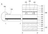
도 1은 본 발명의 제1 실시 예에 따른 터치 패널 일체형 표시 장치를 나타내는 사시도이다.
도 2는 도 1에 도시된 터치 패널의 평면도를 도시한 것이다.
도 3은 도 2를 I-I'와 Ⅱ-Ⅱ'으로 절단한 단면도를 도시한 것이다.
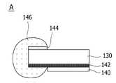
도 4는 도 2에 도시된 차폐 전극 연결부를 나타낸 단면도이다.
도 5a 및 도 5b는 차폐 전극 연결부를 통해 차폐 전극과 차폐 신호 공급 라인이 제대로 연결되었는지 테스트하는 화면을 나타내고 있다.
도 6a 내지 도 6c는 본 발명의 제2 실시 예에 따른 터치 패널의 평면도들을 도시하고 있다.1 is a perspective view illustrating a touch panel integrated type display apparatus according to a first embodiment of the present invention.
FIG. 2 is a plan view of the touch panel shown in FIG. 1. FIG.
FIG. 3 is a cross-sectional view taken along line II 'and II-II' of FIG. 2. FIG.
4 is a cross-sectional view illustrating a shield electrode connection portion shown in FIG.
5A and 5B show a screen for testing whether the shield electrode and the shield signal supply line are properly connected through the shield electrode connection portion.
6A to 6C are top views of a touch panel according to a second embodiment of the present invention.
이하, 첨부된 도면을 참조하여 본 발명에 따른 실시 예를 상세하게 설명한다. 본 발명의 구성 및 그에 따른 작용 효과는 이하의 상세한 설명을 통해 명확하게 이해될 것이다. 본 발명의 상세한 설명에 앞서, 동일한 구성 요소에 대해서는 다른 도면 상에 표시되더라도 가능한 동일한 부호로 표시하며, 공지된 구성에 대해서는 본 발명의 요지를 흐릴 수 있다고 판단되는 경우 구체적인 설명은 생략하기로 함에 유의한다.Hereinafter, embodiments of the present invention will be described in detail with reference to the accompanying drawings. The configuration of the present invention and the operation and effect thereof will be clearly understood through the following detailed description. Before describing the present invention in detail, the same components are denoted by the same reference symbols as possible even if they are displayed on different drawings. In the case where it is judged that the gist of the present invention may be blurred to a known configuration, do.
이하, 본 발명의 바람직한 실시 예를 도 1 내지 도 6c를 참조하여 상세히 설명하기로 한다.Hereinafter, preferred embodiments of the present invention will be described in detail with reference to FIGS. 1 to 6C.
도 1은 본 발명의 제1 실시 예에 따른 터치 패널 일체형 표시 장치를 나타내는 사시도이다. 그리고, 도 2는 도 1에 도시된 터치 패널의 평면도를 도시하고 있으며, 도 3은 도 2를 I-I'와 Ⅱ-Ⅱ'으로 절단한 단면도를 도시한 것이다.1 is a perspective view illustrating a touch panel integrated type display apparatus according to a first embodiment of the present invention. FIG. 2 is a plan view of the touch panel shown in FIG. 1, and FIG. 3 is a cross-sectional view taken along line II 'and II-II' of FIG.
도 1에 도시된 터치 패널 일체형 표시 장치는 액정 패널(110)과, 액정 패널(110) 상에 탑재된 터치 패널(110)를 포함한다. 본 발명의 실시 예로 액정 패널을 예로 들어 설명하지만, 액정 패널 외에 다른 평판 표시 패널도 가능하다.1 includes a
액정 패널(110)은 게이트 라인 및 데이터 라인과 접속된 박막 트랜지스터가 형성된 상부 기판(112)과, 칼러 구현을 위한 칼러 필터가 형성된 하부 기판(114)과, 박막 트랜지스터와 접속되는 화소 전극과, 화소 전극과 수직 전계 또는 수평 전계를 형성하는 공통 전극과, 상부 기판(112)의 전면에 부착된 상부 편광판(118)과, 하부 기판(114)의 배면에 부착된 하부 편광판(116)을 포함한다.The
칼러 필터는 블랙 매트릭스를 기준으로 색이 구분되도록 상부 기판(112) 상에 형성된다. 이 칼러 필터는 R, G, B 별로 형성되어 R, G, B 색상을 구현한다.The color filter is formed on the
공통 전극은 상부 기판(112)의 배면 상에 투명 도전막으로 형성되어 화소 전극과 수직 전계를 이룰 수 있으며, 하부 기판(114) 상에 투명 도전막으로 형성되어 화소 전극과 수평 전계를 이룰 수 있다. 이러한 공통 전극에는 액정 구동을 위한 기준 전압, 즉 공통 전압이 공급된다.The common electrode may be formed as a transparent conductive film on the rear surface of the
박막 트랜지스터는 하부 기판(114) 상에 형성되며 게이트 라인으로부터의 게이트 신호에 응답하여 데이터 라인으로부터의 데이터신호를 선택적으로 화소 전극에 공급한다. 이를 위해, 박막 트랜지스터는 게이트 라인과 접속된 게이트 전극, 데이터 라인과 접속된 소스 전극, 화소 전극과 접속된 드레인 전극, 게이트 전극과 게이트 절연막을 사이에 두고 중첩되면서 소스 전극과 드레인 전극 사이에 채널을 형성하는 활성층, 그 활성층과 소스 전극 및 드레인 전극과의 오믹 접촉을 위한 오믹 접촉층을 구비한다.The thin film transistor is formed on the
화소 전극은 각 화소 영역에서 칼라 필터(R, G, B)와 중첩되도록 독립적으로 형성되고, 박막 트랜지스터의 드레인 전극과 접속된다. 또한, 화소 전극은 액정층을 사이에 두고 공통 전극과 중첩되어 수직 전계를 형성하거나, 동일 기판에 형성되어 수평 전계를 형성한다. 이러한, 화소 전극은 박막 트랜지스터를 통해 데이터 신호가 공급되면, 공통 전압이 공급된 공통 전극과 수직 전계 또는 수평 전계를 형성하여 수직 방향으로 배열된 액정 분자들이 유전율 이방성에 의해 회전하게 된다. 그리고, 액정 분자들의 회전 정도에 따라 화소 영역을 투과하는 광 투과율이 달라지게 됨으로써 계조를 구현하게 된다.The pixel electrodes are independently formed so as to overlap the color filters R, G, and B in each pixel region, and are connected to the drain electrodes of the thin film transistors. Further, the pixel electrode overlaps the common electrode with the liquid crystal layer sandwiched therebetween to form a vertical electric field, or is formed on the same substrate to form a horizontal electric field. When the data signal is supplied to the pixel electrode through the thin film transistor, the liquid crystal molecules aligned in the vertical direction form a vertical electric field or a horizontal electric field with the common electrode supplied with the common voltage to rotate due to the dielectric anisotropy. The transmittance of light passing through the pixel region is changed according to the degree of rotation of the liquid crystal molecules, thereby realizing the gradation.
상부 편광판(118)은 액정 패널(110)의 상부 기판(112)의 상부에 형성된다. 상부 편광판(118)은 액정 패널(110)로부터 입사되는 광에 대해 투과 광량 및 편광 상태를 제어한다.The
하부 편광판(116)은 액정 패널(110)의 하부 기판(12)의 배면에 형성된다. 하부 편광판(116)은 백라이트 유닛으로부터 입사되는 광에 대한 투과 광량 및 편광 상태를 제어한다.The
터치 패널(180)은 위치 감지 전극으로서 기능을 하는 제1 및 제2 전극 패턴부(150,156,160,164)가 형성된 센서 기판(130)과, 센서 기판(130)과 대향하도록 형성된 커버 기판(132)과, 센서 기판(130)의 하부에 전면으로 형성된 차폐 전극(142)과, 차폐 전극(142)과 차폐 신호 공급 라인(144)과 접속시키는 차폐 전극 연결부(146)와, 차폐 전극(142) 배면에 형성된 바텀 절연층(140)과, 액정 패널(110)의 상부 편광판(118) 상에 형성된 제1 점착층(120)과, 센서 기판(130) 상에 형성된 제2 점착층(122)을 포함한다. 여기서, 센서 기판(130)과 커버 기판(132)은 투명 글래스로 형성될 수 있다.The
센서 기판(130)은 제1 전극 패턴부(160,164), 제2 전극 패턴부(150,156), 제1 신호 공급 라인(166), 제2 신호 공급 라인(158), 차폐 신호 공급 라인(144), 센서부 FPC(Flexable Printed Circuit; 이하, FPC)(170)를 구비한다.The
제1 전극 패턴부(160,164)는 제1 방향으로 나란하게 복수개가 형성되어 제1 방향의 정전용량의 변화를 감지한다. 여기서, 제1 방향은 예로 들어 Y축 방향일 수 있다. 제1 전극 패턴부(160,164)는 마름모 형태 또는 다이아몬드 형태의 제1 본체부들(164)과, 서로 인접한 제1 본체부들(164)을 연결하는 연결부들(160)을 포함한다. 이때, 제1 전극 패턴부(160,164)는 제1 신호 공급 라인(166)과 전기적으로 접속되어 신호를 공급받는다. 제1 전극 패턴부(160,164)는 절연층 상에 투명 전극으로 형성되며, 투명 전극 재질로는 ITO(Indium Tin Oxide), IZO(Indium Zinc Oxide), ITZO(Indium Tin Zinc Oxide), ATO(Antimony Tin Oxide) 등의 물질로 형성할 수 있다.A plurality of the first
제2 전극 패턴부(150,156)는 제1 전극 패턴부(160,164)와 교차하도록 제2 방향으로 나란하게 복수개가 형성되어 제2 방향의 정전용량의 변화를 감지한다. 여기서, 제2 방향은 예로 들어 X축 방향일 수 있다. 제2 전극 패턴부(150,156)는 마름모 형태 또는 다이아몬드 형태의 제2 본체들(156)과, 서로 인접한 제2 본체부들(156)을 연결하는 브리지들(150)을 포함한다. 이때, 제2 전극 패턴부의 제2 본체들(156)은 컨택홀(152,154)을 통해 브리지(150)와 접속된다. 제2 전극 패턴부(150,156)는 제2 신호 공급 라인(158)과 전기적으로 접속되어 신호를 공급받는다. 제2 전극 패턴부(150,156)는 절연층 상에 투명 전극으로 형성되며, 투명 전극 재질로는 ITO(Indium Tin Oxide), IZO(Indium Zinc Oxide), ITZO(Indium Tin Zinc Oxide), ATO(Antimony Tin Oxide) 등의 물질로 형성할 수 있다.A plurality of second
차폐 신호 공급 라인(144)은 센서부 FPC(170)와 접속되며, 액정 패널로 유입되는 노이즈를 차단하기 위해 차폐 전극(142)으로 차폐 신호를 공급한다. 이때, 차폐 신호는 액정 패널로 유입되는 노이즈를 차단하기 위해 예를 들어, 접지(GND) 신호일 수 있다. 또한, 센서 기판(130)의 상부에 형성된 차폐 신호 공급 라인(144)과 센서 기판(130)의 하부에 형성된 차폐 전극(142)은 차폐 전극 연결부(146)를 통해 전기적으로 연결된다.The shielding
차폐 전극(142)은 센서 기판(130)의 하부에 전면으로 형성되어, 차폐 신호 공급 라인(144)으로부터 차폐 신호를 공급받아 액정 패널(110)로 유입되는 노이즈(Noise)를 차단한다. 이와 같이, 액정 패널(110)로 유입되는 노이즈를 차폐 전극이 차단함으로써 터치 패널(180)로 인가되는 신호가 액정 패널(110)로 인가되는 신호에 영향을 주지 않게 되어 신호 간의 간섭이 발생하지 않는다. 차폐 전극(142)은 투명 전극으로 형성되며, 투명 전극 재질로는 ITO(Indium Tin Oxide), IZO(Indium Zinc Oxide), ITZO(Indium Tin Zinc Oxide), ATO(Antimony Tin Oxide) 등의 물질로 형성할 수 있다.The shielding
차폐 전극 연결부(146)(A영역)는 센서 기판(130)의 외곽부에 적어도 두 개로 형성되어 센서 기판(130)의 하부의 차폐 전극(142)과, 센서 기판(130)의 상부의 차폐 신호 공급 라인(144)을 연결시킨다. 다시 말하여, 차폐 전극 연결부(146)는 도 3에 도시된 바와 같이 차폐 전극(142)과 차폐 신호 공급 라인(144)을 일부 덮도록 링 형태로 형성되어 차폐 전극(142)과 차폐 신호 공급 라인(144)을 서로 접속시킨다. 차폐 전극 연결부(146)는 도 2 및 도 3에 도시된 바와 같이 센서 기판(130)의 네 모서리에 형성될 수 있으며, 링 형태로 한정되지 않으며 다양한 형태로 형성될 수 있다.The shielding electrode connection part 146 (area A) is formed in at least two outsides of the
이러한, 차폐 전극 연결부(146)는 도전성 재질로 예를 들어, 은(Ag), 도전성 폴리머(Conductive Polymer), 도전 테이프, ITO(Indium Tin Oxide), IZO(Indium Zinc Oxide), ITZO(Indium Tin Zinc Oxide), ATO(Antimony Tin Oxide), 투명 도전 전극 재질, 금속 재질 등으로 형성될 수 있다. 차폐 전극 연결부는 도전성 재질을 도포 방법, 디핑(Dipping) 방법, 스프레이(Spray) 방법, 부착 방법 등으로 형성될 수 있다. 또한, 차폐 전극 연결부(146)는 도 3에 도시된 바와 같이 차폐 전극(142)을 일부 덮도록 형성될 수 있으며, 도 4에 도시된 바와 같이 차폐 전극(142)을 전부 덮도록 형성될 수 있다.The shield
한편, 센서부 FPC(170)와 멀어지는 영역일수록 저항이 커져서 접지 신호(GND)를 제대로 공급받지 못한다. 이에 따라, 센서부 FPC(170)와 멀어지는 영역에 형성된 차폐 전극(14)에는 접지 신호(GND)를 제대로 공급하지 못해 액정 패널로 유입되는 노이즈를 차단하기 어렵게 된다. 하지만, 센서부 FPC(170)와 멀어지는 영역의 모서리 양 끝단에 차폐 전극 연결부(146)를 형성함으로써 균등하게 접지 신호(GND)를 차폐 전극(142)에 공급할 수 있다. 도 5a 및 도 5b는 차폐 전극 연결부를 통해 센서 기판 하부의 차폐 전극과 센서 기판 상부의 차폐 신호 공급 라인이 서로 전기적으로 접속이 잘 되었는지 테스트하기 위해 도전 테이프(190)를 통해 확인하는 화면이고, 화면에 나타나듯이 FPC(170)와 멀어진 영역에라도 차폐 전극 연결부를 통해 차폐 전극과 신호 공급 라인의 접속이 잘 되었음을 나타내고 있다.On the other hand, as the distance from the
또한, 센서 기판(130)의 하부에 형성된 차폐 전극(142)으로 차폐 신호를 공급하기 위해 종래의 터치 패널은 센서 기판(130)의 하부에도 별도의 FPC를 형성하였으나, 별도의 FPC를 형성하지 않아도 차폐 전극 연결부(146)를 통해 차폐 신호가 차폐 전극(142)으로 공급되므로 그에 따른 비용을 감소시킬 수 있다. 그리고, 차폐 전극 연결부(146)는 차폐 전극(142)과 차폐 신호 공급 라인(144)을 전기적으로 접속시키는 것뿐만 아니라, 정전기를 방지할 수 있다.Further, in order to supply the shielding signal to the shielding
제1 점착층(120)은 액정 패널(110)의 상부 편광판(118) 상에 형성되며, 광 투과율이 높은 투명성 접착 재질로 형성된다. 이때, 투명성 접착 재질로는 예를 들어 SVR(Super View Resin) 등으로 이루어질 수 있다.The first
제2 점착층(122)은 센서 기판(130)의 절연층(168) 상에 형성되며, 광 투과율이 높은 투명성 접착 재질로 형성된다. 이때, 투명성 접착 재질로는 예를 들어 SVR(Super View Resin) 등으로 이루어질 수 있다.The second
도 6a 내지 도 6c는 본 발명의 제2 실시 예에 따른 터치 패널을 나타낸 평면도들이다. 본 발명의 제2 실시 예에 따른 터치 패널은 차폐 전극 연결부를 제외한 나머지 구성요소는 동일하므로 생략하기로 한다.6A to 6C are plan views illustrating a touch panel according to a second embodiment of the present invention. The touch panel according to the second embodiment of the present invention is the same as the other components except for the shield electrode connection portion, and thus will not be described.
차폐 전극 연결부(146)는 센서 기판(130)의 외곽부에 적어도 두 개로 형성되어 센서 기판(130)의 하부의 차폐 전극(142)과, 센서 기판(130)의 상부의 차폐 신호 공급 라인(144)을 연결시킨다. 다시 말하여, 차폐 전극 연결부(146)는 차폐 전극(142)과 차폐 신호 공급 라인(144)을 일부 덮도록 링 형태로 형성되어 차폐 전극(142)과 차폐 신호 공급 라인(144)을 서로 접속시킨다. 차폐 전극 연결부(146)는 도 6a에 도시된 바와 같이 센서 기판(130)의 네 모서리와, 네 모서리의 중앙부에 적어도 하나로 형성될 수 있으며, 차폐 전극 연결부(146)는 도 6b 및 도 6c와 같이 센서 기판(130)의 모서리에서 서로 마주보도록 두 개가 형성될 수 있다. 이와 같이, 도 6a 내지 도 6c에 도시된 형태로 차폐 전극 연결부(146)를 형성할 수 있으며, 이에 한정되지 않는다.The shield
이러한, 차폐 전극 연결부(146)는 도전성 재질로 예를 들어, 은(Ag), 도전성 폴리머(Conductive Polymer), 도전 테이프, ITO(Indium Tin Oxide), IZO(Indium Zinc Oxide), ITZO(Indium Tin Zinc Oxide), ATO(Antimony Tin Oxide), 투명 도전 전극 재질, 금속 재질 등으로 형성될 수 있다. 차폐 전극 연결부(146)는 도전성 재질을 도포 방법, 디핑(Dipping) 방법, 스프레이(Spray) 방법, 부착 방법 등으로 형성될 수 있다. 또한, 차폐 전극 연결부(146)는 도 3에 도시된 바와 같이 차폐 전극(142)을 일부 덮도록 형성될 수 있으며, 도 4에 도시된 바와 같이 차폐 전극(142)을 전부 덮도록 형성될 수 있다.The shield
이상의 설명은 본 발명을 예시적으로 설명한 것에 불과하며, 본 발명이 속하는 기술 분야에서 통상의 지식을 가진 자에 의해 본 발명의 기술적 사상에서 벗어나지 않는 범위에서 다양한 변형이 가능할 것이다. 따라서 본 발명의 명세서에 개시된 실시 예들은 본 발명을 한정하는 것이 아니다. 본 발명의 범위는 아래의 특허청구범위에 의해 해석되어야 하며, 그와 균등한 범위 내에 있는 모든 기술도 본 발명의 범위에 포함되는 것으로 해석해야 할 것이다.The foregoing description is merely illustrative of the present invention, and various modifications may be made by those skilled in the art without departing from the spirit of the present invention. Accordingly, the embodiments disclosed in the specification of the present invention are not intended to limit the present invention. The scope of the present invention should be construed according to the following claims, and all the techniques within the scope of equivalents should be construed as being included in the scope of the present invention.
110 : 액정 패널112 : 상부 기판
114 : 하부 기판116 : 하부 편광판
118 : 상부 편광판120, 122 : 제1 및 제2 점착층
130 : 센서 기판132 : 커버 기판
140 : 바텀 절연층142 : 차폐 전극
144 : 차폐 신호 공급 라인146 : 차폐 전극 연결부
150, 156 : 제2 전극 패턴부158 : 제1 신호 공급 라인
160, 164 : 제1 전극 패턴부166 : 제2 신호 공급 라인
170 : 센서부 FPC180 : 터치 패널110: liquid crystal panel 112: upper substrate
114: lower substrate 116: lower polarizer plate
118:
130: sensor substrate 132: cover substrate
140: bottom insulating layer 142: shielding electrode
144: shielding signal supply line 146: shield electrode connection
150, 156: second electrode pattern portion 158: first signal supply line
160, 164: first electrode pattern portion 166: second signal supply line
170: Sensor unit FPC 180: Touch panel
Claims (9)
Translated fromKorean상기 액정 패널 상에 탑재된 터치 패널을 구비하며,
상기 터치 패널은
위치 감지 전극으로서 기능을 하는 제1 및 제2 전극 패턴부가 형성되며, 상부에 차폐 신호를 공급하는 차폐 신호 공급 라인이 형성된 센서 기판과;
상기 센서 기판의 하부에 형성된 차폐 전극과;
상기 차폐 전극과 상기 차폐 신호 공급 라인과 접속시키는 차폐 전극 연결부를 포함하며,
상기 차폐 전극 연결부는 상기 센서 기판 모서리의 외곽부에서 상기 차폐 전극과 상기 차폐 신호 공급 라인 각각을 일부 또는 전부 덮도록 링 형태로 구비되고, 복수개가 서로 이격되도록 배치되는 것을 특징으로 하는 터치 패널 일체형 표시 장치.A liquid crystal panel having an upper substrate and a lower substrate facing each other with a liquid crystal therebetween;
And a touch panel mounted on the liquid crystal panel,
The touch panel
A sensor substrate on which first and second electrode pattern portions functioning as position sensing electrodes are formed and on which a shielding signal supply line for supplying a shielding signal is formed;
A shielding electrode formed on a lower portion of the sensor substrate;
And a shield electrode connection portion connecting the shield electrode and the shield signal supply line,
Wherein the shield electrode connection portion is formed in a ring shape so as to partially or entirely cover the shielding electrode and the shielding signal supply line at the outer edge of the sensor substrate edge, Device.
상기 차폐 전극 연결부는 상기 센서 기판의 외곽부에 적어도 두 개로 형성되어 상기 차폐 전극과 상기 차폐 신호 공급 라인을 접속시키는 것을 특징으로 하는 터치 패널 일체형 표시 장치.The method according to claim 1,
Wherein the shield electrode connection portion is formed on at least two outsides of the sensor substrate to connect the shield electrode and the shield signal supply line.
상기 차폐 전극 연결부는 상기 센서 기판의 네 모서리에 형성되는 것을 특징으로 하는 터치 패널 일체형 표시 장치.The method according to claim 1,
Wherein the shield electrode connection portion is formed at four corners of the sensor substrate.
상기 차폐 전극 연결부는 상기 센서 기판의 네 모서리와 네 모서리의 중앙부에 적어도 하나가 형성되는 것을 특징으로 하는 터치 패널 일체형 표시 장치.The method according to claim 1,
Wherein at least one of the shield electrode connection portions is formed at four corners and four corners of the sensor substrate.
상기 차폐 전극 연결부는 상기 센서 기판의 모서리에서 서로 마주보도록 두 개로 형성되는 것을 특징으로 하는 것을 특징으로 하는 터치 패널 일체형 표시 장치.The method according to claim 1,
Wherein the shield electrode connection portion is formed at two corners of the sensor substrate facing each other at an edge of the sensor substrate.
상기 차폐 전극 연결부는 도전성 재질로 형성되며, 상기 도전성 재질은 은(Ag), 도전성 폴리머(Conductive Polymer), 도전 테이프, ITO(Indium Tin Oxide), IZO(Indium Zinc Oxide), ITZO(Indium Tin Zinc Oxide), ATO(Antimony Tin Oxide), 투명 도전 전극 재질, 금속 재질인 것을 특징으로 하는 터치 패널 일체형 표시 장치.The method according to claim 1,
The shielding electrode connection portion is formed of a conductive material and the conductive material may be at least one selected from the group consisting of Ag, Conductive Polymer, Conductive Tape, Indium Tin Oxide (ITO), Indium Zinc Oxide (IZO), Indium Tin Zinc Oxide ), ATO (Antimony Tin Oxide), a transparent conductive electrode material, and a metal material.
상기 차폐 전극 연결부는 도전성 재질을 도포 방법, 디핑(Dipping) 방법, 스프레이(Spray) 방법, 부착 방법으로 형성하는 것을 특징으로 하는 터치 패널 일체형 표시 장치.The method according to claim 1,
Wherein the shielding electrode connection portion is formed of a conductive material by a coating method, a dipping method, a spraying method, or an attaching method.
Priority Applications (3)
| Application Number | Priority Date | Filing Date | Title |
|---|---|---|---|
| KR1020100093641AKR101686108B1 (en) | 2010-09-28 | 2010-09-28 | Display device associated with touch panel |
| US13/226,901US8810534B2 (en) | 2010-09-28 | 2011-09-07 | Display device with an embedded touch panel and a method of manufacturing the same |
| CN201110319062.5ACN102436323B (en) | 2010-09-28 | 2011-09-16 | Display device associated with touch panel and producing method thereof |
Applications Claiming Priority (1)
| Application Number | Priority Date | Filing Date | Title |
|---|---|---|---|
| KR1020100093641AKR101686108B1 (en) | 2010-09-28 | 2010-09-28 | Display device associated with touch panel |
Publications (2)
| Publication Number | Publication Date |
|---|---|
| KR20120032158A KR20120032158A (en) | 2012-04-05 |
| KR101686108B1true KR101686108B1 (en) | 2016-12-14 |
Family
ID=45870139
Family Applications (1)
| Application Number | Title | Priority Date | Filing Date |
|---|---|---|---|
| KR1020100093641AExpired - Fee RelatedKR101686108B1 (en) | 2010-09-28 | 2010-09-28 | Display device associated with touch panel |
Country Status (3)
| Country | Link |
|---|---|
| US (1) | US8810534B2 (en) |
| KR (1) | KR101686108B1 (en) |
| CN (1) | CN102436323B (en) |
Cited By (1)
| Publication number | Priority date | Publication date | Assignee | Title |
|---|---|---|---|---|
| US10635211B2 (en) | 2017-04-24 | 2020-04-28 | Samsung Display Co., Ltd. | Display module |
Families Citing this family (40)
| Publication number | Priority date | Publication date | Assignee | Title |
|---|---|---|---|---|
| CN102999199B (en)* | 2011-09-16 | 2016-08-10 | 宸鸿科技(厦门)有限公司 | Touch sensing device and electronic installation |
| JP5840522B2 (en)* | 2012-02-08 | 2016-01-06 | 株式会社ジャパンディスプレイ | Touch panel, display device and electronic device |
| US9253892B2 (en)* | 2012-04-13 | 2016-02-02 | Wistron Corporation | Peripheral circuit of touch panel and manufacturing method thereof |
| CN102778987A (en)* | 2012-06-29 | 2012-11-14 | 华为终端有限公司 | Projection type capacitance touch screen and preparation method thereof |
| US20140022199A1 (en)* | 2012-07-19 | 2014-01-23 | Texas Instruments Incorporated | Capacitive touch panel having improved response characteristics |
| CN103677366B (en)* | 2012-09-20 | 2018-01-16 | 宸鸿科技(厦门)有限公司 | Touch panel module, contactor control device and preparation method thereof |
| KR102045809B1 (en)* | 2012-12-13 | 2019-11-18 | 엘지디스플레이 주식회사 | Touch sensor integrated type display device |
| CN103913869B (en)* | 2012-12-31 | 2017-06-23 | 上海天马微电子有限公司 | Liquid crystal display with embedded touch device and forming method thereof |
| WO2014113983A1 (en)* | 2013-01-28 | 2014-07-31 | Texas Instruments Incorporated | Capacitive single layer multi-touch panel having improved response characteristics |
| JP2014211720A (en)* | 2013-04-17 | 2014-11-13 | 富士通株式会社 | Display apparatus and display control program |
| TW201445387A (en)* | 2013-05-22 | 2014-12-01 | Henghao Technology Co Ltd | Printing method for shielding layer of touch panel |
| KR102135908B1 (en) | 2013-06-26 | 2020-07-21 | 엘지디스플레이 주식회사 | Touch sensing apparatus and method for driving the same |
| TWI520025B (en)* | 2013-12-17 | 2016-02-01 | 友達光電股份有限公司 | Capacitive touch display panel, capacitive touch panel and manufacturing method thereof |
| KR102178796B1 (en) | 2014-01-22 | 2020-11-16 | 삼성디스플레이 주식회사 | Display device |
| KR102237926B1 (en)* | 2014-02-05 | 2021-04-08 | 엘지이노텍 주식회사 | Touch window |
| TWI537801B (en)* | 2014-03-20 | 2016-06-11 | 原相科技股份有限公司 | Noise-cancelled capacitive touch display apparatus |
| CN103941952B (en) | 2014-03-31 | 2017-03-29 | 上海天马微电子有限公司 | Electromagnetic induction type touch substrate and inductive touch display device |
| US9904417B2 (en)* | 2014-04-16 | 2018-02-27 | Microchip Technology Incorporated | Projected capacitive touch detection with touch force detection using self-capacitance and mutual capacitance detection |
| CN106662941A (en)* | 2014-07-03 | 2017-05-10 | 夏普株式会社 | Touch panel substrate |
| TWI554916B (en)* | 2014-07-21 | 2016-10-21 | 晨星半導體股份有限公司 | Touch display panel |
| KR102411328B1 (en)* | 2014-07-25 | 2022-06-21 | 삼성디스플레이 주식회사 | Display Device |
| KR102262470B1 (en)* | 2014-11-28 | 2021-06-08 | 삼성디스플레이 주식회사 | Touch screen panel manufacturing method |
| US9285913B1 (en) | 2014-12-31 | 2016-03-15 | Lg Display Co., Ltd. | Display device and driving method thereof |
| US9939972B2 (en) | 2015-04-06 | 2018-04-10 | Synaptics Incorporated | Matrix sensor with via routing |
| KR20160120401A (en)* | 2015-04-07 | 2016-10-18 | 삼성디스플레이 주식회사 | Touch screen panel, display device including the same, and driving method thereof |
| US9671915B2 (en) | 2015-06-30 | 2017-06-06 | Synaptics Incorporated | Avoidance of bending effects in a touch sensor device |
| US9971463B2 (en) | 2015-09-29 | 2018-05-15 | Synaptics Incorporated | Row-based sensing on matrix pad sensors |
| KR20170039025A (en)* | 2015-09-30 | 2017-04-10 | 삼성디스플레이 주식회사 | Display device |
| CN105353921B (en)* | 2015-12-08 | 2018-01-23 | 上海天马微电子有限公司 | Integrated touch display panel and touch display device |
| KR102536878B1 (en)* | 2016-01-26 | 2023-05-26 | 삼성디스플레이 주식회사 | Touch panel and display apparatus including the same |
| CN106843616B (en)* | 2017-01-03 | 2020-05-19 | 京东方科技集团股份有限公司 | Touch substrate, manufacturing method thereof and touch display device |
| CN107092400B (en)* | 2017-06-27 | 2019-10-01 | 上海天马微电子有限公司 | Touch display panel and touch display device comprising same |
| KR102553525B1 (en)* | 2018-06-29 | 2023-07-10 | 엘지디스플레이 주식회사 | Touch display panel, touch display device |
| US11003278B2 (en)* | 2018-12-27 | 2021-05-11 | Lg Display Co., Ltd. | Touch display device, driving circuit, and driving method |
| US11695018B2 (en) | 2019-06-28 | 2023-07-04 | E Ink Holdings Inc. | Display apparatus |
| CN110502154B (en)* | 2019-08-30 | 2023-06-20 | 京东方科技集团股份有限公司 | Touch panel, touch display screen and display device |
| CN112721821A (en)* | 2019-10-28 | 2021-04-30 | 常州星宇车灯股份有限公司 | Waterproof tail mark of car touch |
| CN112817469A (en)* | 2019-11-15 | 2021-05-18 | 京东方科技集团股份有限公司 | Touch substrate and manufacturing method thereof, touch display substrate and touch display device |
| CN110955074A (en)* | 2019-12-12 | 2020-04-03 | 深圳市华星光电半导体显示技术有限公司 | Liquid crystal display panel and electronic device |
| EP4343373A1 (en)* | 2022-09-21 | 2024-03-27 | LX Semicon Co., Ltd. | Image sensing apparatus, electronic apparatus including the same, and driving method of image sensing apparatus |
Citations (3)
| Publication number | Priority date | Publication date | Assignee | Title |
|---|---|---|---|---|
| US20050110103A1 (en)* | 2003-09-24 | 2005-05-26 | Authentec, Inc. | Finger biometric sensor with sensor electronics distributed over thin film and monocrystalline substrates and related methods |
| US20080203279A1 (en) | 2007-02-26 | 2008-08-28 | Epson Imaging Devices Corporation | Electro-optical device, semiconductor device, display device, and electronic apparatus having the display device |
| JP2009098834A (en)* | 2007-10-16 | 2009-05-07 | Epson Imaging Devices Corp | Capacitance type input device, display device with input function and electronic equipment |
Family Cites Families (5)
| Publication number | Priority date | Publication date | Assignee | Title |
|---|---|---|---|---|
| JPH06348392A (en)* | 1993-06-10 | 1994-12-22 | Seiko Epson Corp | Tablet |
| US5940526A (en)* | 1997-05-16 | 1999-08-17 | Harris Corporation | Electric field fingerprint sensor having enhanced features and related methods |
| JP4784528B2 (en) | 2007-02-26 | 2011-10-05 | ソニー株式会社 | Electro-optical device, semiconductor device, display device, and electronic apparatus including the same |
| JP5394655B2 (en)* | 2008-04-28 | 2014-01-22 | 株式会社ジャパンディスプレイ | Liquid crystal display |
| CN101634922B (en) | 2009-08-21 | 2012-01-11 | 深圳莱宝高科技股份有限公司 | Wiring structure and manufacturing method of capacitive touch screen |
- 2010
- 2010-09-28KRKR1020100093641Apatent/KR101686108B1/ennot_activeExpired - Fee Related
- 2011
- 2011-09-07USUS13/226,901patent/US8810534B2/enactiveActive
- 2011-09-16CNCN201110319062.5Apatent/CN102436323B/ennot_activeExpired - Fee Related
Patent Citations (3)
| Publication number | Priority date | Publication date | Assignee | Title |
|---|---|---|---|---|
| US20050110103A1 (en)* | 2003-09-24 | 2005-05-26 | Authentec, Inc. | Finger biometric sensor with sensor electronics distributed over thin film and monocrystalline substrates and related methods |
| US20080203279A1 (en) | 2007-02-26 | 2008-08-28 | Epson Imaging Devices Corporation | Electro-optical device, semiconductor device, display device, and electronic apparatus having the display device |
| JP2009098834A (en)* | 2007-10-16 | 2009-05-07 | Epson Imaging Devices Corp | Capacitance type input device, display device with input function and electronic equipment |
Cited By (4)
| Publication number | Priority date | Publication date | Assignee | Title |
|---|---|---|---|---|
| US10635211B2 (en) | 2017-04-24 | 2020-04-28 | Samsung Display Co., Ltd. | Display module |
| US11243625B2 (en) | 2017-04-24 | 2022-02-08 | Samsung Display Co., Ltd. | Display module |
| US11720193B2 (en) | 2017-04-24 | 2023-08-08 | Samsung Display Co., Ltd. | Display module |
| US12307033B2 (en) | 2017-04-24 | 2025-05-20 | Samsung Display Co., Ltd. | Display module |
Also Published As
| Publication number | Publication date |
|---|---|
| KR20120032158A (en) | 2012-04-05 |
| US8810534B2 (en) | 2014-08-19 |
| CN102436323B (en) | 2015-06-10 |
| CN102436323A (en) | 2012-05-02 |
| US20120075214A1 (en) | 2012-03-29 |
Similar Documents
| Publication | Publication Date | Title |
|---|---|---|
| KR101686108B1 (en) | Display device associated with touch panel | |
| KR101908492B1 (en) | Display device associated with touch panel | |
| US8610859B2 (en) | Liquid crystal display device associated with touch panel and method for fabricating the same | |
| KR101009672B1 (en) | Touch Panel Built-in Liquid Crystal Display | |
| KR101319347B1 (en) | Liquid Crystal Display Panel Associated with Touch Panel | |
| KR101230196B1 (en) | Liquid Crystal Display having a Touch Screen Panel | |
| US8692948B2 (en) | Electric field shielding for in-cell touch type thin-film-transistor liquid crystal displays | |
| US9158419B2 (en) | Touch panel | |
| EP2209039A1 (en) | Touch screen panel | |
| US10656476B2 (en) | Liquid crystal panel | |
| CN107407984A (en) | Display panel with touch detection | |
| US20130033452A1 (en) | Display device | |
| KR101901253B1 (en) | Display Device integrating with Touch Screen and Method for Manufacturing the Same | |
| KR20100031243A (en) | Liquid crystal display device | |
| KR20080050674A (en) | Liquid crystal display | |
| KR101658149B1 (en) | Display Device Including Touch Panel | |
| US9019221B2 (en) | Display device integrated with touch screen panel | |
| KR101706234B1 (en) | Touch panel and display device associated with the same | |
| KR101859469B1 (en) | Display device and manufacturing method thereof | |
| KR101818468B1 (en) | Manufacturing method of display device | |
| KR101768488B1 (en) | Display device | |
| KR20120063355A (en) | Display device associated with touch panel and manufacturing method thereof |
Legal Events
| Date | Code | Title | Description |
|---|---|---|---|
| PA0109 | Patent application | St.27 status event code:A-0-1-A10-A12-nap-PA0109 | |
| R18-X000 | Changes to party contact information recorded | St.27 status event code:A-3-3-R10-R18-oth-X000 | |
| R18-X000 | Changes to party contact information recorded | St.27 status event code:A-3-3-R10-R18-oth-X000 | |
| R18-X000 | Changes to party contact information recorded | St.27 status event code:A-3-3-R10-R18-oth-X000 | |
| PG1501 | Laying open of application | St.27 status event code:A-1-1-Q10-Q12-nap-PG1501 | |
| R17-X000 | Change to representative recorded | St.27 status event code:A-3-3-R10-R17-oth-X000 | |
| A201 | Request for examination | ||
| PA0201 | Request for examination | St.27 status event code:A-1-2-D10-D11-exm-PA0201 | |
| D13-X000 | Search requested | St.27 status event code:A-1-2-D10-D13-srh-X000 | |
| D14-X000 | Search report completed | St.27 status event code:A-1-2-D10-D14-srh-X000 | |
| E902 | Notification of reason for refusal | ||
| PE0902 | Notice of grounds for rejection | St.27 status event code:A-1-2-D10-D21-exm-PE0902 | |
| E13-X000 | Pre-grant limitation requested | St.27 status event code:A-2-3-E10-E13-lim-X000 | |
| P11-X000 | Amendment of application requested | St.27 status event code:A-2-2-P10-P11-nap-X000 | |
| P13-X000 | Application amended | St.27 status event code:A-2-2-P10-P13-nap-X000 | |
| E701 | Decision to grant or registration of patent right | ||
| PE0701 | Decision of registration | St.27 status event code:A-1-2-D10-D22-exm-PE0701 | |
| GRNT | Written decision to grant | ||
| PR0701 | Registration of establishment | St.27 status event code:A-2-4-F10-F11-exm-PR0701 | |
| PR1002 | Payment of registration fee | St.27 status event code:A-2-2-U10-U11-oth-PR1002 Fee payment year number:1 | |
| PG1601 | Publication of registration | St.27 status event code:A-4-4-Q10-Q13-nap-PG1601 | |
| PC1903 | Unpaid annual fee | St.27 status event code:A-4-4-U10-U13-oth-PC1903 Not in force date:20191208 Payment event data comment text:Termination Category : DEFAULT_OF_REGISTRATION_FEE | |
| PC1903 | Unpaid annual fee | St.27 status event code:N-4-6-H10-H13-oth-PC1903 Ip right cessation event data comment text:Termination Category : DEFAULT_OF_REGISTRATION_FEE Not in force date:20191208 | |
| P22-X000 | Classification modified | St.27 status event code:A-4-4-P10-P22-nap-X000 |