KR101685057B1 - Stacked package of semiconductor device - Google Patents
Stacked package of semiconductor deviceDownload PDFInfo
- Publication number
- KR101685057B1 KR101685057B1KR1020100006126AKR20100006126AKR101685057B1KR 101685057 B1KR101685057 B1KR 101685057B1KR 1020100006126 AKR1020100006126 AKR 1020100006126AKR 20100006126 AKR20100006126 AKR 20100006126AKR 101685057 B1KR101685057 B1KR 101685057B1
- Authority
- KR
- South Korea
- Prior art keywords
- semiconductor chip
- bonding pads
- semiconductor
- leads
- interposer
- Prior art date
- Legal status (The legal status is an assumption and is not a legal conclusion. Google has not performed a legal analysis and makes no representation as to the accuracy of the status listed.)
- Active
Links
Images


Classifications
- H—ELECTRICITY
- H01—ELECTRIC ELEMENTS
- H01L—SEMICONDUCTOR DEVICES NOT COVERED BY CLASS H10
- H01L23/00—Details of semiconductor or other solid state devices
- H01L23/28—Encapsulations, e.g. encapsulating layers, coatings, e.g. for protection
- H01L23/31—Encapsulations, e.g. encapsulating layers, coatings, e.g. for protection characterised by the arrangement or shape
- H01L23/3107—Encapsulations, e.g. encapsulating layers, coatings, e.g. for protection characterised by the arrangement or shape the device being completely enclosed
- H—ELECTRICITY
- H01—ELECTRIC ELEMENTS
- H01L—SEMICONDUCTOR DEVICES NOT COVERED BY CLASS H10
- H01L23/00—Details of semiconductor or other solid state devices
- H01L23/48—Arrangements for conducting electric current to or from the solid state body in operation, e.g. leads, terminal arrangements ; Selection of materials therefor
- H01L23/488—Arrangements for conducting electric current to or from the solid state body in operation, e.g. leads, terminal arrangements ; Selection of materials therefor consisting of soldered or bonded constructions
- H01L23/495—Lead-frames or other flat leads
- H01L23/49575—Assemblies of semiconductor devices on lead frames
- H—ELECTRICITY
- H01—ELECTRIC ELEMENTS
- H01L—SEMICONDUCTOR DEVICES NOT COVERED BY CLASS H10
- H01L24/00—Arrangements for connecting or disconnecting semiconductor or solid-state bodies; Methods or apparatus related thereto
- H01L24/73—Means for bonding being of different types provided for in two or more of groups H01L24/10, H01L24/18, H01L24/26, H01L24/34, H01L24/42, H01L24/50, H01L24/63, H01L24/71
- H—ELECTRICITY
- H01—ELECTRIC ELEMENTS
- H01L—SEMICONDUCTOR DEVICES NOT COVERED BY CLASS H10
- H01L25/00—Assemblies consisting of a plurality of semiconductor or other solid state devices
- H01L25/18—Assemblies consisting of a plurality of semiconductor or other solid state devices the devices being of the types provided for in two or more different main groups of the same subclass of H10B, H10D, H10F, H10H, H10K or H10N
- H—ELECTRICITY
- H01—ELECTRIC ELEMENTS
- H01L—SEMICONDUCTOR DEVICES NOT COVERED BY CLASS H10
- H01L2224/00—Indexing scheme for arrangements for connecting or disconnecting semiconductor or solid-state bodies and methods related thereto as covered by H01L24/00
- H01L2224/01—Means for bonding being attached to, or being formed on, the surface to be connected, e.g. chip-to-package, die-attach, "first-level" interconnects; Manufacturing methods related thereto
- H01L2224/02—Bonding areas; Manufacturing methods related thereto
- H01L2224/04—Structure, shape, material or disposition of the bonding areas prior to the connecting process
- H01L2224/05—Structure, shape, material or disposition of the bonding areas prior to the connecting process of an individual bonding area
- H01L2224/0554—External layer
- H01L2224/0555—Shape
- H01L2224/05552—Shape in top view
- H01L2224/05554—Shape in top view being square
- H—ELECTRICITY
- H01—ELECTRIC ELEMENTS
- H01L—SEMICONDUCTOR DEVICES NOT COVERED BY CLASS H10
- H01L2224/00—Indexing scheme for arrangements for connecting or disconnecting semiconductor or solid-state bodies and methods related thereto as covered by H01L24/00
- H01L2224/01—Means for bonding being attached to, or being formed on, the surface to be connected, e.g. chip-to-package, die-attach, "first-level" interconnects; Manufacturing methods related thereto
- H01L2224/18—High density interconnect [HDI] connectors; Manufacturing methods related thereto
- H01L2224/23—Structure, shape, material or disposition of the high density interconnect connectors after the connecting process
- H01L2224/24—Structure, shape, material or disposition of the high density interconnect connectors after the connecting process of an individual high density interconnect connector
- H01L2224/241—Disposition
- H01L2224/24135—Connecting between different semiconductor or solid-state bodies, i.e. chip-to-chip
- H01L2224/24145—Connecting between different semiconductor or solid-state bodies, i.e. chip-to-chip the bodies being stacked
- H—ELECTRICITY
- H01—ELECTRIC ELEMENTS
- H01L—SEMICONDUCTOR DEVICES NOT COVERED BY CLASS H10
- H01L2224/00—Indexing scheme for arrangements for connecting or disconnecting semiconductor or solid-state bodies and methods related thereto as covered by H01L24/00
- H01L2224/01—Means for bonding being attached to, or being formed on, the surface to be connected, e.g. chip-to-package, die-attach, "first-level" interconnects; Manufacturing methods related thereto
- H01L2224/26—Layer connectors, e.g. plate connectors, solder or adhesive layers; Manufacturing methods related thereto
- H01L2224/31—Structure, shape, material or disposition of the layer connectors after the connecting process
- H01L2224/32—Structure, shape, material or disposition of the layer connectors after the connecting process of an individual layer connector
- H01L2224/321—Disposition
- H01L2224/32135—Disposition the layer connector connecting between different semiconductor or solid-state bodies, i.e. chip-to-chip
- H01L2224/32145—Disposition the layer connector connecting between different semiconductor or solid-state bodies, i.e. chip-to-chip the bodies being stacked
- H—ELECTRICITY
- H01—ELECTRIC ELEMENTS
- H01L—SEMICONDUCTOR DEVICES NOT COVERED BY CLASS H10
- H01L2224/00—Indexing scheme for arrangements for connecting or disconnecting semiconductor or solid-state bodies and methods related thereto as covered by H01L24/00
- H01L2224/01—Means for bonding being attached to, or being formed on, the surface to be connected, e.g. chip-to-package, die-attach, "first-level" interconnects; Manufacturing methods related thereto
- H01L2224/42—Wire connectors; Manufacturing methods related thereto
- H01L2224/47—Structure, shape, material or disposition of the wire connectors after the connecting process
- H01L2224/48—Structure, shape, material or disposition of the wire connectors after the connecting process of an individual wire connector
- H01L2224/481—Disposition
- H01L2224/48135—Connecting between different semiconductor or solid-state bodies, i.e. chip-to-chip
- H01L2224/48145—Connecting between different semiconductor or solid-state bodies, i.e. chip-to-chip the bodies being stacked
- H01L2224/48147—Connecting between different semiconductor or solid-state bodies, i.e. chip-to-chip the bodies being stacked with an intermediate bond, e.g. continuous wire daisy chain
- H—ELECTRICITY
- H01—ELECTRIC ELEMENTS
- H01L—SEMICONDUCTOR DEVICES NOT COVERED BY CLASS H10
- H01L2224/00—Indexing scheme for arrangements for connecting or disconnecting semiconductor or solid-state bodies and methods related thereto as covered by H01L24/00
- H01L2224/01—Means for bonding being attached to, or being formed on, the surface to be connected, e.g. chip-to-package, die-attach, "first-level" interconnects; Manufacturing methods related thereto
- H01L2224/42—Wire connectors; Manufacturing methods related thereto
- H01L2224/47—Structure, shape, material or disposition of the wire connectors after the connecting process
- H01L2224/48—Structure, shape, material or disposition of the wire connectors after the connecting process of an individual wire connector
- H01L2224/481—Disposition
- H01L2224/48151—Connecting between a semiconductor or solid-state body and an item not being a semiconductor or solid-state body, e.g. chip-to-substrate, chip-to-passive
- H01L2224/48221—Connecting between a semiconductor or solid-state body and an item not being a semiconductor or solid-state body, e.g. chip-to-substrate, chip-to-passive the body and the item being stacked
- H01L2224/48245—Connecting between a semiconductor or solid-state body and an item not being a semiconductor or solid-state body, e.g. chip-to-substrate, chip-to-passive the body and the item being stacked the item being metallic
- H01L2224/48247—Connecting between a semiconductor or solid-state body and an item not being a semiconductor or solid-state body, e.g. chip-to-substrate, chip-to-passive the body and the item being stacked the item being metallic connecting the wire to a bond pad of the item
- H—ELECTRICITY
- H01—ELECTRIC ELEMENTS
- H01L—SEMICONDUCTOR DEVICES NOT COVERED BY CLASS H10
- H01L2224/00—Indexing scheme for arrangements for connecting or disconnecting semiconductor or solid-state bodies and methods related thereto as covered by H01L24/00
- H01L2224/01—Means for bonding being attached to, or being formed on, the surface to be connected, e.g. chip-to-package, die-attach, "first-level" interconnects; Manufacturing methods related thereto
- H01L2224/42—Wire connectors; Manufacturing methods related thereto
- H01L2224/47—Structure, shape, material or disposition of the wire connectors after the connecting process
- H01L2224/49—Structure, shape, material or disposition of the wire connectors after the connecting process of a plurality of wire connectors
- H01L2224/491—Disposition
- H01L2224/4912—Layout
- H01L2224/49171—Fan-out arrangements
- H—ELECTRICITY
- H01—ELECTRIC ELEMENTS
- H01L—SEMICONDUCTOR DEVICES NOT COVERED BY CLASS H10
- H01L2224/00—Indexing scheme for arrangements for connecting or disconnecting semiconductor or solid-state bodies and methods related thereto as covered by H01L24/00
- H01L2224/01—Means for bonding being attached to, or being formed on, the surface to be connected, e.g. chip-to-package, die-attach, "first-level" interconnects; Manufacturing methods related thereto
- H01L2224/42—Wire connectors; Manufacturing methods related thereto
- H01L2224/47—Structure, shape, material or disposition of the wire connectors after the connecting process
- H01L2224/49—Structure, shape, material or disposition of the wire connectors after the connecting process of a plurality of wire connectors
- H01L2224/491—Disposition
- H01L2224/4912—Layout
- H01L2224/49175—Parallel arrangements
- H—ELECTRICITY
- H01—ELECTRIC ELEMENTS
- H01L—SEMICONDUCTOR DEVICES NOT COVERED BY CLASS H10
- H01L2224/00—Indexing scheme for arrangements for connecting or disconnecting semiconductor or solid-state bodies and methods related thereto as covered by H01L24/00
- H01L2224/73—Means for bonding being of different types provided for in two or more of groups H01L2224/10, H01L2224/18, H01L2224/26, H01L2224/34, H01L2224/42, H01L2224/50, H01L2224/63, H01L2224/71
- H01L2224/732—Location after the connecting process
- H01L2224/73251—Location after the connecting process on different surfaces
- H01L2224/73265—Layer and wire connectors
- H—ELECTRICITY
- H01—ELECTRIC ELEMENTS
- H01L—SEMICONDUCTOR DEVICES NOT COVERED BY CLASS H10
- H01L2225/00—Details relating to assemblies covered by the group H01L25/00 but not provided for in its subgroups
- H01L2225/03—All the devices being of a type provided for in the same main group of the same subclass of class H10, e.g. assemblies of rectifier diodes
- H01L2225/04—All the devices being of a type provided for in the same main group of the same subclass of class H10, e.g. assemblies of rectifier diodes the devices not having separate containers
- H01L2225/065—All the devices being of a type provided for in the same main group of the same subclass of class H10
- H01L2225/06503—Stacked arrangements of devices
- H01L2225/06555—Geometry of the stack, e.g. form of the devices, geometry to facilitate stacking
- H01L2225/06562—Geometry of the stack, e.g. form of the devices, geometry to facilitate stacking at least one device in the stack being rotated or offset
- H—ELECTRICITY
- H01—ELECTRIC ELEMENTS
- H01L—SEMICONDUCTOR DEVICES NOT COVERED BY CLASS H10
- H01L24/00—Arrangements for connecting or disconnecting semiconductor or solid-state bodies; Methods or apparatus related thereto
- H01L24/01—Means for bonding being attached to, or being formed on, the surface to be connected, e.g. chip-to-package, die-attach, "first-level" interconnects; Manufacturing methods related thereto
- H01L24/42—Wire connectors; Manufacturing methods related thereto
- H01L24/47—Structure, shape, material or disposition of the wire connectors after the connecting process
- H01L24/48—Structure, shape, material or disposition of the wire connectors after the connecting process of an individual wire connector
- H—ELECTRICITY
- H01—ELECTRIC ELEMENTS
- H01L—SEMICONDUCTOR DEVICES NOT COVERED BY CLASS H10
- H01L24/00—Arrangements for connecting or disconnecting semiconductor or solid-state bodies; Methods or apparatus related thereto
- H01L24/01—Means for bonding being attached to, or being formed on, the surface to be connected, e.g. chip-to-package, die-attach, "first-level" interconnects; Manufacturing methods related thereto
- H01L24/42—Wire connectors; Manufacturing methods related thereto
- H01L24/47—Structure, shape, material or disposition of the wire connectors after the connecting process
- H01L24/49—Structure, shape, material or disposition of the wire connectors after the connecting process of a plurality of wire connectors
- H—ELECTRICITY
- H01—ELECTRIC ELEMENTS
- H01L—SEMICONDUCTOR DEVICES NOT COVERED BY CLASS H10
- H01L2924/00—Indexing scheme for arrangements or methods for connecting or disconnecting semiconductor or solid-state bodies as covered by H01L24/00
- H01L2924/0001—Technical content checked by a classifier
- H01L2924/00014—Technical content checked by a classifier the subject-matter covered by the group, the symbol of which is combined with the symbol of this group, being disclosed without further technical details
- H—ELECTRICITY
- H01—ELECTRIC ELEMENTS
- H01L—SEMICONDUCTOR DEVICES NOT COVERED BY CLASS H10
- H01L2924/00—Indexing scheme for arrangements or methods for connecting or disconnecting semiconductor or solid-state bodies as covered by H01L24/00
- H01L2924/15—Details of package parts other than the semiconductor or other solid state devices to be connected
- H01L2924/181—Encapsulation
Landscapes
- Engineering & Computer Science (AREA)
- Microelectronics & Electronic Packaging (AREA)
- Computer Hardware Design (AREA)
- Power Engineering (AREA)
- Physics & Mathematics (AREA)
- Condensed Matter Physics & Semiconductors (AREA)
- General Physics & Mathematics (AREA)
- Wire Bonding (AREA)
- Lead Frames For Integrated Circuits (AREA)
Abstract
Translated fromKoreanDescription
Translated fromKorean본 발명은 반도체 소자의 적층 패키지 및 그 제조 방법에 관한 것으로, 보다 구체적으로는 양면 적층 리드 프레임 구조의 반도체 적층 패키지 및 그 제조 방법에 관한 것이다.BACKGROUND OF THE
최근 반도체 산업의 발전과 사용자의 요구에 따라 전자기기는 더욱 소형화 및 경량화되고 있으며 이에 따라 전자기기의 핵심 부품인 반도체 소자 또한 소형화 및 경량화되고 있다. 이에 따라 복수의 반도체 소자를 하나의 제품으로 구성하는 기술이 개발되고 있다. 복수의 반도체 소자를 하나의 제품으로 구성하기 위하여, 여러 반도체 칩을 적층하고 상호 연결하여 구성하는 멀티 칩 패키지(MCP; Multi-Chip Package)가 제조되고 있다. 멀티 칩 패키지로는 볼(Ball)을 가지는 비지에이(BGA) 패키지 형태와 제조 비용의 감소 및 보다 많은 수의 적층을 위하여 양면 적층이 가능한 리드 프레임(Lead Frame) 패키지 형태가 제공되고 있다.2. Description of the Related Art In recent years, electronic devices have become smaller and lighter in accordance with the development of the semiconductor industry and users' demands. As a result, semiconductor devices, which are core components of electronic devices, are also becoming smaller and lighter. As a result, a technique of forming a plurality of semiconductor elements into one product has been developed. In order to constitute a plurality of semiconductor devices as one product, a multi-chip package (MCP) in which a plurality of semiconductor chips are stacked and interconnected is manufactured. A multi-chip package is provided in the form of a BGA package having balls, and a lead frame package type capable of stacking both sides for a reduction in manufacturing cost and a larger number of stacks.
본 발명은 반도체 칩들을 효율적으로 양면으로 적층 할 수 있는 반도체 소자 적층 패키지 구조를 제공한다.The present invention provides a semiconductor device stack package structure capable of efficiently stacking semiconductor chips on both sides.
또한, 본 발명은 상기 반도체 소자의 적층 패키지를 제공하는데 적합한 반도체 소자의 적층 패키지 제조 방법을 제공한다.The present invention also provides a method of manufacturing a stacked package of semiconductor devices suitable for providing a stacked package of semiconductor devices.
본 발명은 반도체 소자의 적층 패키지를 제공한다. 반도체 소자의 적층 패키지는 전기적으로 분리된 인터포저 리드들; 상기 인터포저 리드의 일 표면상에 위치되며, 다수의 본딩 패드들을 가지는 적어도 하나의 제 1 반도체 칩; 상기 인터포저 리드의 다른 표면상에 위치되며, 다수의 본딩 패드들을 가지는 적어도 하나의 제 2 반도체 칩; 상기 제 1 반도체 칩 상에 위치되며 다수의 본딩 패드들을 가지는, 그리고 상기 제 1 반도체 칩 및 상기 제 2 반도체 칩과 그 기능을 달리하는 제 3 반도체 칩; 상기 제 3 반도체 칩의 본딩 패드와 외부 간에 전기적 연결을 위한 외부 접속 리드들; 및 상기 제 1 반도체 칩, 상기 제 2 반도체 칩, 상기 제 3 반도체 칩, 상기 인터포저 리드들, 및 상기 외부 접속 리드들 간에 전기적 연결을 하는 와이어 본딩 수단을 포함하며, 상기 인터포저 리드들은 상기 제 1 반도체 칩들 및 상기 제 2 반도체 칩 간에 전기적 연결 매개체로서 제공될 수 있다.The present invention provides a stacked package of semiconductor devices. A stacked package of semiconductor devices includes electrically isolated interposer leads; At least one first semiconductor chip located on one surface of the interposer lid and having a plurality of bonding pads; At least one second semiconductor chip located on the other surface of the interposer lead and having a plurality of bonding pads; A third semiconductor chip positioned on the first semiconductor chip and having a plurality of bonding pads and having a function different from that of the first semiconductor chip and the second semiconductor chip; External connection leads for electrical connection between the bonding pads of the third semiconductor chip and the outside; And wire bonding means for making an electrical connection between the first semiconductor chip, the second semiconductor chip, the third semiconductor chip, the interposer leads, and the external connection leads, 1 semiconductor chips and the second semiconductor chip.
상기 제 1 반도체 칩 및 상기 제 2 반도체 칩은 메모리 반도체일 수 있다. 또한, 상기 제 3 반도체 칩은 메모리 컨트롤러 반도체일 수 있다.The first semiconductor chip and the second semiconductor chip may be memory semiconductors. The third semiconductor chip may be a memory controller semiconductor.
또한, 외부 접속 리드들 중 전원 역할의 외부 접속 리드는 상기 제 1 반도체 칩 또는 상기 제 2 반도체 칩 상의 본딩 패드들 중 대응되는 전원 본딩 패드에 본딩 와이어로 직접 연결될 수 있다.The external connection leads acting as power sources among the external connection leads may be directly connected to the corresponding power bonding pads among the bonding pads on the first semiconductor chip or the second semiconductor chip as bonding wires.
또한, 외부 접속 리드들 중 전원 역할의 외부 접속 리드는 상기 인터포저 리드들 중 전원 역할의 인터포저 리드에 본딩 와이어로 직접 연결될 수 있다.Also, among the external connection leads, the external connection leads serving as the power source may be directly connected to the interposer leads acting as power sources among the interposer leads by the bonding wires.
또한, 외부 접속 리드들 중 전원 역할의 외부 접속 리드와 상기 인터포저 리드들 중 전원 역할의 인터포저 리드는 일체로 제공될 수 있다.Also, among the external connection leads, an external connection lead serving as a power source and an interposer lead serving as a power source among the interposer leads may be integrally provided.
각각의 상기 외부 접속 리드의 일부, 상기 제 1 반도체 칩, 상기 제 2 반도체 칩, 상기 제 3 반도체 칩, 그리고 상기 인터포저 리드들을 덮도록 몰딩 수지가 제공될 수 있다.A molding resin may be provided to cover a part of each of the external connection leads, the first semiconductor chip, the second semiconductor chip, the third semiconductor chip, and the interposer leads.
상기 제 1 반도체 칩 및 상기 제 2 반도체 칩은 각각 복수 개가 제공되고, 상기 제 1 반도체 칩들과 상기 제 2 반도체 칩들은 각각 오프셋(Off-set)을 가지는 계단방식으로 적층될 수 있다.A plurality of the first semiconductor chips and the second semiconductor chips may be provided, respectively, and the first semiconductor chips and the second semiconductor chips may be stacked in a stepwise manner having offsets.
상기 와이어 본딩 수단은 인접한 상기 본딩 패드끼리 상호 연결하는 점핑 본딩(Jumping Bonding) 방식으로 제공될 수 있다.The wire bonding means may be provided in a jumping bonding manner in which adjacent bonding pads are connected to each other.
상기 제 1 반도체 칩 및 상기 제 2 반도체 칩 각각에서 상기 본딩 패드들은 상기 제 1 반도체 칩 또는 상기 제 2 반도체 칩에서 상기 인터포저 리드와 마주보는 면의 반대 측의 가장자리 영역에 그 모서리를 따라 일렬로 정렬되도록 배치될 수 있다.The bonding pads in each of the first semiconductor chip and the second semiconductor chip are arranged in an edge area on the opposite side of the face facing the interposer lead in the first semiconductor chip or the second semiconductor chip in a line As shown in FIG.
상기 제 1 반도체 칩, 상기 제 2 반도체 칩, 그리고 제 3 반도체 칩들 중 적어도 어느 하나의 상기 본딩 패드들은 웨이퍼 레벨 공정시 만들어진 칩 패드에서 재배선(Redistributed Layout)으로 형성되는 재배선 패드일 수 있다. 상기 제 3 반도체 칩의 크기는 상기 제 1 반도체 칩 및 상기 제 2 반도체 칩의 크기보다 작게 제공될 수 있다.The bonding pads of at least any one of the first semiconductor chip, the second semiconductor chip, and the third semiconductor chip may be rewiring pads formed in a redistributed layout in a chip pad formed in a wafer level process. The size of the third semiconductor chip may be smaller than the size of the first semiconductor chip and the second semiconductor chip.
상기 제 3 반도체 칩과 인접한 상기 제 1 반도체 칩에는 더미 본딩 패드들이 더 형성되며, 상기 더미 본딩 패드는 상기 제 3 반도체 칩의 본딩 패드 및 상기 외부 접속 리드 각각에 직접 본딩 와이어로 전기적 연결될 수 있다.Dummy bonding pads may be further formed on the first semiconductor chip adjacent to the third semiconductor chip and the dummy bonding pads may be electrically connected to the bonding pads of the third semiconductor chip and the external connection leads directly with bonding wires.
각각의 상기 인터포저 리드는 바 형상으로 제공되고, 상기 인터포저 리드들은 서로 간에 이격되며 상기 인터포저 리드의 길이 방향에 수직한 방향을 따라 일렬로 배열될 수 있다.Each of the interposer leads is provided in a bar shape, and the interposer leads may be spaced apart from each other and arranged in a line along a direction perpendicular to the longitudinal direction of the interposer leads.
상기 제 1 반도체 칩들은 상기 인터포저 리드로부터 멀어질수록 상기 인터포저 리드의 일단을 향해 오프셋 되고, 상기 제 2 반도체 칩들은 상기 인터포저 리드로부터 멀어질수록 상기 인터포저 리드의 타단을 향해 오프셋 될 수 있다.The first semiconductor chips are offset toward one end of the interposer lead away from the interposer lead and the second semiconductor chips can be offset toward the other end of the interposer lead away from the interposer lead have.
상기 더미 본딩 패드들은 상기 제 1 반도체 칩의 가장자리 영역들 중 상기 제 1 반도체 칩의 본딩 패드들이 제공된 가장자리 영역과 수직한 가장자리 영역에 제공될 수 있다.The dummy bonding pads may be provided in an edge region of the edge regions of the first semiconductor chip perpendicular to an edge region provided with bonding pads of the first semiconductor chip.
또한, 본 발명은 반도체 소자의 적층 패키지를 제조하는 방법을 제공한다. 상기 방법은 전기적으로 분리된 복수의 인터포저 리드를 제공하는 단계; 상기 복수의 인터포저 리드의 일면 상에 적어도 하나의 제 1 반도체 칩을 제공하는 단계; 상기 복수의 인터포저 리드의 타면 상에 적어도 하나의 제 2 반도체 칩을 제공하는 단계; 상기 제 1 반도체 칩 상에 제 3 반도체 칩을 적층하는 단계; 상기 제 1 반도체 칩, 상기 제 2 반도체 칩, 상기 제 3 반도체 칩의 대응되는 기능의 본딩 패드들을 상호 전기적 연결 수단으로 접속하고, 상기 제 1 반도체 칩과 상기 제 2 반도체 칩의 본딩 패드를 상기 복수의 인터포저 리드와 상호 전기적 연결 수단으로 접속하는 단계; 상기 제 3 반도체 칩에서 외부와의 입력/출력을 담당하는 본딩 패드를 외부 접속 리드에 상호 전기적 연결 수단으로 접속하는 단계; 및 상기 제 1 반도체 칩, 상기 제 2 반도체 칩, 상기 제 3 반도체 칩, 상기 인터포저 리드들, 그리고 상기 외부 접속 리드 일부를 덮도록 몰딩 수지를 충진하는 단계를 포함한다.The present invention also provides a method of manufacturing a stacked package of semiconductor devices. The method includes providing a plurality of electrically isolated interposer leads; Providing at least one first semiconductor chip on one side of the plurality of interposer leads; Providing at least one second semiconductor chip on the other side of the plurality of interposer leads; Stacking a third semiconductor chip on the first semiconductor chip; And bonding pads of corresponding functions of the first semiconductor chip, the second semiconductor chip and the third semiconductor chip are connected to each other by electrical connection means, and the bonding pads of the first semiconductor chip and the second semiconductor chip are connected to each other With an interposer lead of the first electrode; Connecting a bonding pad for input / output to / from the outside of the third semiconductor chip to an external connection lead through mutual electrical connection means; And filling the molding resin to cover the first semiconductor chip, the second semiconductor chip, the third semiconductor chip, the interposer leads, and a part of the external connection lead.
상기 제 1 반도체 칩과 상기 제 2 반도체 칩은 각각 복수 개가 적층되게 제공되고, 상기 제 1 반도체 칩들은 상기 인터포저 리드로부터 멀어질수록 상기 인터포저 리드의 일단을 향해 오프셋 되고, 상기 제 2 반도체 칩들은 상기 인터포저 리드로부터 멀어질수록 상기 인터포저 리드의 타단을 향해 오프셋 될 수 있다.Wherein the first semiconductor chip and the second semiconductor chip are provided so as to be stacked, respectively, and the first semiconductor chips are offset toward one end of the interposer lead as the distance from the interposer lead is increased, May be offset toward the other end of the interposer lead away from the interposer lead.
상기 제 1 반도체 칩들, 상기 제 2 반도체 칩들, 그리고 상기 제 3 반도체 칩들 간에 전기적 연결하는 와이어 본딩 방식은 인접하는 상기 본딩 패드들끼리 상호 연결하는 점핑 본딩(Jumping Bonding) 방식일 수 있다.The wire bonding method for electrically connecting the first semiconductor chips, the second semiconductor chips, and the third semiconductor chips may be a jumping bonding method in which adjacent bonding pads are connected to each other.
상기 제 1 반도체 칩, 상기 제 2 반도체 칩, 또는 상기 제 3 반도체 칩의 본딩 패드들은 재배선(Redistributed Layout)공정으로 진행하여 형성될 수 있다.The bonding pads of the first semiconductor chip, the second semiconductor chip, or the third semiconductor chip may be formed in a redistributed layout process.
상기 외부 접속 리드와 상기 제 3 반도체 칩의 전기적 연결은 상기 제 3 반도체 칩과 인접한 상기 제 1 반도체 칩 상에 더미 본딩 패드들을 형성하고, 상기 제 3 반도체 칩의 본딩 패드들과 상기 더미 본딩 패드, 그리고 상기 더미 본딩 패드와 상기 외부 접속 리드를 와이어 본딩하여 이루어질 수 있다.Wherein the external connection lead and the third semiconductor chip are electrically connected to each other by forming dummy bonding pads on the first semiconductor chip adjacent to the third semiconductor chip and bonding bonding pads of the third semiconductor chip and the dummy bonding pads, And bonding the dummy bonding pad and the external connection lead by wire bonding.
상술한 바와 같이 본 발명에 의한 반도체 소자 적층 패키지는 인터포저 리드의 양면에 각각 메모리 칩을 적층하고 인터포저 리드의 일면에 컨트롤러 칩을 제공할 때 인터포저 리드의 일면에 위치한 컨트롤러 칩과 다른 면에 위치한 메모리 칩을 전기적으로 연결하는 것이 가능하다.As described above, in the semiconductor device laminate package according to the present invention, when memory chips are stacked on both sides of an interposer lead and a controller chip is provided on one side of the interposer lead, It is possible to electrically connect the located memory chip.
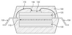
도 1은 본 발명의 일 실시 예에 의한 반도체 소자의 적층 패키지를 개략적으로 보여주는 사시도이다.
도 2는 도 1의 선 A-A를 따라 절단한 단면도이다.
도 3은 도 1의 선 B-B를 따라 절단한 단면도이다.
도 4 내지 도 9는 도 1의 반도체 소자의 적층 패키지를 제조하는 과정을 보여주는 도면들이다.
도 10은 본 발명의 다른 실시예에 의한 반도체 소자의 적층 패키지를 개략적으로 보여주는 사시도이다.
도 11은 도 10의 선 C-C를 따라 절단한 단면도이다.
도 12 내지 도 16은 각각 반도체 소자의 적층 패키지의 변형된 예를 보여주는 단면도들이다.1 is a perspective view schematically showing a stacked package of semiconductor devices according to an embodiment of the present invention.
2 is a cross-sectional view taken along line AA of FIG.
3 is a cross-sectional view taken along the line BB in Fig.
FIGS. 4 to 9 are views showing a process of manufacturing the laminated package of the semiconductor device of FIG.
10 is a perspective view schematically showing a stacked package of semiconductor devices according to another embodiment of the present invention.
11 is a cross-sectional view taken along the line CC of Fig.
12 to 16 are sectional views showing a modified example of the stacked package of semiconductor devices, respectively.
상술한 본 발명의 양상은 첨부된 도면을 참조하여 설명되는 바람직한 실시 예들을 통하여 더욱 명백해질 것이다. 이하에서는 바람직한 실시 예를 통해 당업자가 본 발명을 용이하게 이해하고 재현할 수 있도록 상세히 설명하기로 한다. 그러나 다음에 예시하는 본 발명의 실시 예는 여러 가지 다른 형태로 변형될 수 있으며 본 발명의 범위가 다음에 상술하는 실시 예에 한정되는 것은 아니다. 본 발명의 실시 예는 당 업계에서 통상의 지식을 가진 자에게 본 발명을 더욱 완전하게 설명하기 위하여 제공되는 것이다.The above-mentioned aspects of the present invention will become more apparent through the preferred embodiments described with reference to the accompanying drawings. DETAILED DESCRIPTION OF THE PREFERRED EMBODIMENTS Hereinafter, embodiments of the present invention will be described in detail with reference to the accompanying drawings. However, the following embodiments of the present invention can be modified into various other forms, and the scope of the present invention is not limited to the following embodiments. Embodiments of the present invention are provided to more fully describe the present invention to those skilled in the art.
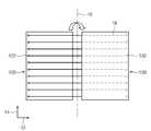
도 1 내지 도 3은 본 발명의 실시 예에 의한 반도체 소자의 적층 패키지(100)를 개략적으로 보여주는 도면이다. 도 1은 반도체 소자의 적층 패키지(100)를 상부에서 바라본 도면이고, 도 2는 도 1의 선 A-A를 따라 절단한 단면도이고, 도 3은 도 2의 선 B-B를 따라 절단한 단면도이다. 도 1에서 실질적으로 몰딩 된 내부는 외부에서 보이지 않으나, 설명의 편의를 위해 몰딩된 부분의 내부를 도시하였다. 이하, 설명의 편의를 위해 인터포저 리드의 길이 방향을 제 1 방향(12)이라 칭하고, 상부에서 바라볼 때 제 1 방향과 수직한 방향을 제 2 방향(14)이라 칭한다.1 to 3 are views schematically showing a stacked
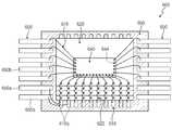
도 1 내지 도 3을 참조하면, 반도체 소자의 적층 패키지(100)는 리드 프레임 구조의 패키지이다. 반도체 소자의 적층 패키지(100)는 인터포저 리드들(110), 제 1 반도체 칩들(120), 제 2 반도체 칩들(130), 제 3 반도체 칩(140), 외부 접속 리드들(150), 그리고 몰딩 수지(160)를 포함한다.Referring to Figs. 1 to 3, the semiconductor
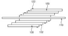
인터포저 리드들(110)은 반도체 소자의 적층 패키지(100) 안에 존재하는 반도체 칩들(120,130,140)의 서브스트레이트(Substrate) 역할을 할 수 있다. 제 1 반도체 칩들(120)은 인터포저 리드(120)의 상면에 적층되게 배치되고 제 2 반도체 칩들(130)은 인터포저 리드(120)의 하면에 적층되게 배치될 수 있다. 제 1 반도체 칩들(120)과 제 2 반도체 칩들(130)은 데이터 저장 역할을 수행할 수 있다. 제 1 반도체 칩(120)과 제 2 반도체 칩(130)은 동일한 수로 제공될 수 있다. 제 1 반도체 칩(120)들 중 가장 상단에 위치된 반도체 칩(120a) 상에는 제 3 반도체 칩(140)이 장착될 수 있다. 선택적으로 제 3 반도체 칩(140)은 제 2 반도체 칩들(130) 중 가장 하단에 위치된 반도체 칩(130a) 상에 장착될 수 있다. 제 1 반도체 칩(120) 및 제 2 반도체 칩(130)은 동일한 종류의 칩이고, 제 1 반도체 칩(120)과 제 3 반도체 칩(140)은 서로 다른 종류의 반도체 칩일 수 있다. 예컨대, 제 1 반도체 칩(120)과 제 2 반도체 칩(130)은 메모리 반도체이고, 제 3 반도체 칩(140)은 메모리 컨트롤러 반도체일 수 있다. 제 1 반도체 칩(120)은 낸드 플래쉬(NAND Flash) 디바이스이고, 제 3 반도체 칩(140)은 그 낸드 플래쉬 디바이스를 제어하는 컨트롤러 디바이스일 수 있다. 낸드 플래쉬 디바이스는 3 비트 낸드 플래쉬일 수 있다. 제 3 반도체 칩(140)은 제 1 반도체 칩(120)보다 작은 크기로 제공될 수 있다.The interposer leads 110 may act as a substrate of the
제 1 반도체 칩(120)과 제 2 반도체 칩(130)은 각각 본딩 패드들(122, 132)을 가진다. 제 1 반도체 칩(120)에서 본딩 패드들(122)은 제 1 반도체 칩(120)의 가장자리 영역에 배치될 수 있다. 또한, 제 1 반도체 칩들(120)의 본딩 패드들(122)은 제 1 반도체 칩(120)에서 인터포저 리드(110)와 마주보는 면의 반대측에 형성될 수 있다. 또한, 본딩 패드들(122)은 일렬로 배열될 수 있다. 예컨대, 본딩 패드들(122)의 배열 방향은 제 2 방향(14)에 평행한 방향일 수 있다. 제 2 반도체 칩(130)에서 본딩 패드들(132)은 제 1 반도체 칩(120)의 본딩 패드들(122)과 동일하게 제공될 수 있다. 따라서 제 2 반도체 칩(130)의 본딩 패드들(132)은 제 2 반도체 칩(130)에서 인터포저 리드(110)와 마주보는 면의 반대측에 형성될 수 있다.The
제 3 반도체 칩(140)은 제 1 본딩 패드들(142)과 제 2 본딩 패드들(144)을 가진다. 제 1 본딩 패드들(142)과 제 2 본딩 패드들(144)은 제 3 반도체 칩(140)에서 인터포저 리드(110)와 마주보는 면의 반대측에 형성될 수 있다. 제 1 본딩 패드들(142)은 제 3 반도체 칩(140)의 제 1 가장자리 영역(145)에 배치되고, 제 2 본딩 패드들(144)은 제 1 가장자리 영역(145)에 수직한 제 2 가장자리 영역(146)에 배치될 수 있다. 제 1 본딩 패드들(142)은 제 2 방향에 평행한 방향으로 일렬로 배열될 수 있다. 제 2 가장자리 영역(146)에 배치된 제 2 본딩 패드들(144)은 제 1 방향(12)에 평행한 방향으로 일렬로 배열될 수 있다. 또한, 제 2 본딩 패드들(144)은 추가적으로 제 2 가장자리 영역(146)과 마주보는 제 3 가장자리 영역(147)에 제 1 방향(12)에 평행한 방향으로 일렬로 배열될 수 있다.The
인터포저 리드들(110)은 서로 간에 전기적으로 분리되게 배치된다. 분리된 인터포저 리드들(110)은 같은 기능을 수행하는 제 1 반도체 칩들(120)의 본딩 패드들(122)과 제 2 반도체 칩들(130)의 본딩 패드들(132)을 상호 전기적으로 연결하는 매개체 기능을 수행한다. 인터포저 리드(110)들은 입력/출력 단자를 고려하여 필요한 개 수만큼 제공될 수 있다. 각각의 인터포저 리드(110)는 바(bar) 형상으로 제공될 수 있다. 인터포저 리드들(110)은 서로 간에 동일한 형상 및 크기로 제공될 수 있다. 인터포저 리드들(110)은 서로 간에 이격되며 제 2 방향(14)을 따라 일렬로 배열될 수 있다. 인접하는 인터포저 리드들(110) 간의 간격은 동일하게 제공될 수 있다.The interposer leads 110 are disposed to be electrically separated from each other. The separated interposer leads 110 electrically connect the
제 1 반도체 칩들(120) 중 인터포저 리드(110)에 가장 인접한 제 1 반도체 칩(120b)의 본딩 패드들(122)은 이에 대응되는 인터포저 리드(110)에 전기적 연결 수단인 본딩 와이어(170)에 의해 접속될 수 있다. 제 2 반도체 칩들(130) 중 인터포저 리드(110)에 가장 인접한 제 2 반도체 칩(130b)의 본딩 패드들(132)은 이에 대응되는 인터포저 리드(110)에 본딩 와이어(170)에 의해 전기적으로 접속될 수 있다. 따라서 인터포저 리드(110)를 매개로 하여 인터포저 리드(110)의 서로 다른 면에 제공된 제1 반도체 칩(120)과 제 2 반도체 칩(130)이 전기적으로 연결될 수 있다. 또한, 인접하는 제 1 반도체 칩들(120)의 본딩 패드들(122)은 서로 대응되는 본딩 패드들(122) 간에 본딩 와이어(170)에 의해 전기적으로 연결되고, 인접하는 제 2 반도체 칩들(130) 상의 본딩 패드들(132)은 서로 대응되는 본딩 패드들(132) 간에 본딩 와이어(170)에 의해 전기적으로 연결될 수 있다. 또한, 제 3 반도체 칩(140) 상의 제 1 본딩 패드(132)는 제 3 반도체 칩(140)과 가장 인접하게 위치된 제 1 반도체 칩(120a) 상의 대응되는 본딩 패드(122)와 본딩 와이어(170)에 의해 전기적으로 연결될 수 있다. 상기 제 3 반도체 칩(140)의 제 2 본딩 패드(144)는 대응되는 외부 접속 리드(150)와 본딩 와이어(170)에 의해 전기적으로 연결될 수 있다.
도 2를 다시 참조하면, 제 1 반도체 칩들(120)은 오프셋(Off-set)을 가지는 계단방식으로 적층 될 수 있다. 제 1 반도체 칩들(120)을 연결하는 본딩 와이어(170)의 본딩 방식은 인접한 제 1 반도체 칩(120)의 본딩 패드들(122)끼리 상호 연결하는 점핑 본당(Jumping Bonding) 방식 일 수 있다. 제 2 반도체 칩(130)은 오프셋(Off-set)을 가지는 계단 방식으로 적층 될 수 있다. 제 2 반도체 칩들(130)을 연결하는 본딩 와이어(170)의 본딩 방식은 인접한 제 2 반도체 칩(130)의 본딩 패드들(132)끼리 상호 연결하는 점핑 본딩 방식일 수 있다. 제 1 반도체 칩들(120)은 인터포저 리드(110)로부터 멀어질수록 인터포저 리드(110)의 일단(112)을 향해 오프셋 되고, 제 2 반도체 칩들(130)은 인터포저 리드(110)로부터 멀어질수록 인터포저 리드(110)의 타단(114)을 향해 오프셋 될 수 있다. 제 1 반도체 칩들(120) 간에 오프셋되는 거리는 서로 동일하고, 제 2 반도체 칩들(130) 간에 오프셋되는 거리는 서로 동일할 수 있다. 이때, 인터포저 리드(110)에 가장 인접한 제 1 반도체 칩(120b)과 인터포저 리드(110)에 가장 인접한 제 2 반도체 칩(130b)은 상부에서 바라볼 때 완전히 중첩되도록 위치될 수 있다.Referring again to FIG. 2, the
몰딩 수지(160)는 인터포저 리드들(110), 제 1 반도체 칩들(120), 제 2 반도체 칩들(130), 제 3 반도체 칩(140), 각 외부 접속 리드(160)의 일부분, 그리고 본딩 와이어들(170)을 덮도록 제공된다.The
도 4 내지 도 9는 반도체 소자의 적층 패키지(100)를 제조하는 순서에 포함되는 공정들을 도시한 것이다.Figs. 4 to 9 show processes included in the order of manufacturing the
먼저, 인터포저 리드들(110)이 서로 간에 분리된 상태로 제 2 방향(14)을 따라 일렬로 제공된다. 다음에 제 1 반도체 칩들(120)이 제공된다. 제 1 반도체 칩(120)은 본딩 패드(122)가 그 상면에 위치되게 제공된다. 제 1 반도체 칩들(120)이 인터포저 리드(110)의 상면 상에 서로 간에 제 1 방향(12)으로 오프셋 되도록 적층된다. 따라서 제 1 반도체 칩(120)은 본딩 패드들(122)이 인터포저 리드(110)와 마주보는 면의 반대측에 위치되도록 제공된다. 이후 제 2 반도체 칩들(130)이 제공된다. 제 2 반도체 칩(130)은 제 1 반도체 칩(120)과 동일한 종류로 제공한다. 도 4와 같이 제 2 반도체 칩(130)은 제 2 방향(14)에 평행한 직선(16)을 기준으로 180도(˚) 회전된 상태로 인터포저 리드(110)의 하면 상에 제공된다. 제 2 반도체 칩(130)은 제 1 방향(12)을 따라 서로 간에 오프셋 된 상태로 적층되게 제공된다. 제 2 반도체 칩들(130)이 오프셋되는 방향은 제 1 반도체 칩들이 오프셋되는 방향과 반대로 제공된다. 제 1 반도체 칩(120)과 제 2 반도체 칩(130)에서 같은 기능의 본딩 패드들(122, 132)은 위에서 보면 제 1 방향(12)에 평행한 직선(18) 상에 위치된다. 따라서 인터포저 리드들(110), 제 1 반도체 칩들(120), 그리고 제 2 반도체 칩들(130)은 도 5 및 도 6과 같이 제공될 수 있다. 도 5는 인터포저 리드들(110), 제 1 반도체 칩들(120), 그리고 제 2 반도체 칩들(130) 간의 상대 위치를 정면에서 바라본 도면이고, 도 6은 이들을 상부에서 바라본 도면이다.First, the interposer leads 110 are provided in a line along the
도 7을 참조하면, 제 3 반도체 칩(140)은 제 1 반도체 칩들(120) 중 가장 상단에 위치한 제 1 반도체 칩(120a) 위에 적층될 수 있다. 제 1 반도체 칩들(120), 제 2 반도체 칩들(130), 그리고 제 3 반도체 칩(140)의 적층이 완료되면 인접하는 제 1 반도체 칩들(120)에서 대응되는 본딩 패드들(122)을 본딩 와이어(170)로 상호 연결한다. 또한, 인접하는 제 2 반도체 칩들(130)에서 대응되는 본딩 패드들(132)을 본딩 와이어(170)로 상호 연결한다. 또한, 가장 상단에 위치하는 제 1 반도체 칩(120a)의 본딩 패드들(122)과 제 3 반도체 칩(140)에서 대응되는 제 1 본딩 패드들(142)을 본딩 와이어(170)로 상호 연결한다. 또한, 인터포저 리드(110)와 가장 인접한 제 1 반도체 칩(120b)의 본딩 패드(122)를 이에 대응하는 인터포저 리드(110)에 본딩 와이어(170)로 상호 연결한다. 또한, 인터포저 리드(110)와 가장 인접한 제 2 반도체 칩(130b)의 본딩 패드(132)를 이에 대응하는 인터포저 리드(110)에 본딩 와이어(170)로 상호 연결한다. 본딩 방식은 점핑 본딩 방식으로 진행할 수 있다.Referring to FIG. 7, the
도 8을 참조하면, 인터포저 리드(110)에 전기적 접속을 진행하는 동시 또는 선후 공정에 있어서 제 3 반도체 칩(140) 상의 제 2 본딩 패드(144)를 본딩 와이어(170)를 통하여 외부와의 입력 출력을 담당하는 외부 접속 단자들(150)과 전기적 연결을 진행한다.8, the
이후, 도 9와 같이 몰딩 수지(160)로 인터포저 리드들(110), 제 1 반도체 칩들(120), 제 2 반도체 칩들(130), 제 3 반도체 칩(140), 외부 접속 리드(150)의 일부, 그리고 본딩 와이어들(170)을 덮는다.9, the interposer leads 110, the
제 1 반도체 칩(120), 제 2 반도체 칩(130), 그리고 제 3 반도체 칩(140) 상의 본딩 패드들(122, 132, 142)은 효율적인 본딩와이어 공정을 위하여 웨이퍼 레벨 공정시 만들어진 패드에서 재배선(Redistributed Layout) 형성 기술을 사용하여 형성될 수 있다. 도 10과 도 11은 재배선 형성 기술이 적용된 반도체 소자 적층 패키지(200)의 실시예를 보여준다. 도 10은 반도체 소자 적층 패키지(200)의 사시도이고, 도 11은 도 10의 선 C-C를 따라 절단한 단면도이다. 도 10과 도 11을 참고하면, 반도체 소자 적층 패키지(200)는 도 1의 반도체 소자 적층 패키지(100)와 대체로 유사한 구조를 가진다. 제 3 반도체 칩(240)의 크기가 제 1 반도체 칩(220)의 크기보다 작을 수 있기 때문에, 제 1 반도체 칩들(220) 중 제 3 반도체 칩(240)과 인접한 제 1 반도체 칩(220a)은 더미 본딩 패드들(224)을 더 가진다. 더미 본딩 패드(224)는 제 1 반도체 칩(220a)의 내부 회로와는 절연되게 제공될 수 있다. 인접하는 더미 본딩 패드들(224) 간의 간격은 제 3 반도체 칩(240)의 인접하는 제 2 본딩 패드 (244) 간의 간격보다 넓게 제공될 수 있다. 제 1 반도체 칩(220a)에서 본딩 패드들(224)이 제공된 영역을 제 1 가장자리 영역(225)이라 할 때, 더미 본딩 패드들(224)은 제 1 가장자리 영역(225)에 수직한 제 2 가장자리 영역(226)에 배치될 수 있다. 더미 본딩 패드들(224)은 제 1 방향(12)을 따라 일렬로 배열될 수 있다. 또한, 더미 본딩 패드들(224)은 제 2 가장자리 영역(226)과 마주보는 제 3 가장자리 영역(227)에도 제 1 방향(12)을 따라 일렬로 배열될 수 있다. 선택적으로 더미 본딩 패드(224)는 제 1 반도체 칩(220)의 영역들 중 제 3 반도체 칩(240)의 모서리 근처에 제공될 수 있다.The
제 3 반도체 칩(240)의 제 2 본딩 패드들(244)과 외부 접속 리드들(250) 간에 전기적 접속은 다음과 같이 이루어질 수 있다. 먼저, 제 3 반도체 칩(240)의 제 2 본딩 패드(244)와 이에 대응하는 제 1 반도체 칩(220)의 더미 본딩 패드(224)를 와이어 본딩(270)에 의해 전기적으로 접속하고, 이후 더미 본딩 패드(224)와 이에 대응하는 외부 접속 리드(250)를 와이어 본딩(270)에 의해 전기적으로 접속한다. 더미 본딩 패드(224)의 제공에 의해 제 3 반도체 칩(240)과 외부 접속 리드(250)의 전기적 연결을 위한 본딩 와이어(270)의 길이를 짧게 할 수 있다.The electrical connection between the
상술한 바와 달리 도 12와 같이 반도체 소자의 적층 패키지(300)에서 제 1 반도체 칩들(320) 중 인터포저 리드(310)에 가장 인접한 제 1 반도체 칩(320b)과 제 2 반도체 칩들(330) 중 인터포저 리드(310)에 가장 인접한 제 2 반도체 칩(330b)은 상부에서 바라볼 때 일부만 중첩되게 제공될 수 있다. 이 경우 제 2 반도체 칩(330b)은 제 1 반도체 칩(320b)에 대해 제 1 반도체 칩들(320)이 서로 간에 오프셋되는 방향으로 오프셋 되게 제공될 수 있다.12, a
선택적으로 도 13의 반도체 소자의 적층 패키지(400)와 같이 제 2 반도체 칩들(430) 중 인터포저 리드(410)에 가장 인접한 제 2 반도체 칩(430b)은 제 1 반도체 칩들(420) 중 인터포저 리드(410)에 가장 인접한 제 1 반도체 칩(420b)에 대해 제 1 반도체 칩들(420)이 서로 간에 오프셋되는 방향과 반대 방향으로 오프셋되게 제공될 수 있다.The
상술한 바와 달리 도 14와 같이 반도체 소자의 적층 패키지(500)에서 외부 접속 리드들(550) 중 전원인 파워 및 그라운드 역할의 외부 접속 리드(550a)는 제 1 반도체 칩(510)의 본딩 패드들(512) 또는 제 2 반도체 칩(520) 상의 본딩 패드들(522) 중 대응되는 전원 본딩 패드(522a)에 본딩 와이어(570)로 직접 연결될 수 있다. 그리고 나머지 외부 접속 리드들(550b)은 제 3 반도체 칩(540)의 제 2 본딩 패드들(544)에 직접 연결될 수 있다. 나머지 외부 접속 리드들(550b)은 제 3 반도체 칩(540)의 제 2 본딩 패드들(544)에 직접 연결될 수 있다. 이와 달리 외부 접속 리드(550a)는 인터포저 리드(510)와 가장 인접하게 배치된 제 1 반도체 칩(520a)이나 제 2 반도체 칩(530a) 이외의 제 1 반도체 칩(520)이나 제 2 반도체 칩(530)에 본딩 와이어로 직접 연결될 수 있다.14, external connection leads 550a serving as a power source and ground of the external connection leads 550 in the semiconductor
선택적으로 도 15와 같이 반도체 소자의 적층 패키지(600)에서 외부 접속 리드들(650) 중 전원인 파워 및 그라운드 기능의 외부 접속 리드(650a)는 인터포저 리드들(610) 중 전원 역할의 인터포저 리드(610a)에 본딩 와이어(670)로 직접 연결될 수 있다. 나머지 외부 접속 리드들(650b)은 제 3 반도체 칩(640)의 제 2 본딩 패드들(644)에 직접 연결될 수 있다.15, the
선택적으로 도 16과 같이 반도체 소자의 적층 패키지(700)에서 외부 접속 리드들(750) 중 전원인 파워 및 그라운드 기능의 외부 접속 리드(750a)와 인터포저 리드들(710) 중 전원 역할의 인터포저 리드(710a)는 일체로 형성될 수 있다. 예컨대, 외부 접속 리드(750a)와 인터포저 리드(710a)는 하나의 리드로서 제공되거나, 서로 간에 직접 연결될 수 있다.As shown in FIG. 16, the external connection leads 750a and the interposer leads 710 of the external connection leads 750, which are power sources and ground functions, The
도 14 내지 도 16의 예에서 외부 접속 리드들 중 인터포저 리드 또는 제 1 반도체 칩이나 제 2 반도체 칩에 연결되는 전원용 접속 리드의 수는 도시된 바와 상이할 수 있다.In the examples of Figs. 14 to 16, the number of connection leads for the power supply connected to the interposer leads or the first semiconductor chip or the second semiconductor chip among the external connection leads may be different from that shown.
상술한 예에서는 제 1 반도체 칩과 제 2 반도체 칩이 복수 개 제공되는 것으로 설명하였다. 그러나 이와 달리 제 1 반도체 칩과 제 2 반도체 칩은 1개씩 제공될 수 있다. 또한, 상술한 예에서는 제 1 반도체 칩과 제 2 반도체 칩이 동일한 수로 제공되는 것으로 설명하였다. 그러나 이와 달리 제 1 반도체 칩과 제 2 반도체 칩은 서로 상이한 수로 제공될 수 있다.In the above-described example, a plurality of the first semiconductor chip and the second semiconductor chip are provided. Alternatively, the first semiconductor chip and the second semiconductor chip may be provided one by one. In the above-described example, the first semiconductor chip and the second semiconductor chip are provided in the same number. Alternatively, however, the first semiconductor chip and the second semiconductor chip may be provided in different numbers from each other.
100 : 적층 패키지 110 : 인터포저 리드
120 : 제 1 반도체 칩 130 : 제 2 반도체 칩
140 : 제 3 반도체 칩 150 : 외부 접속 리드
160 : 몰딩 부재 170 : 본딩 와이어100: stacked package 110: interposer lead
120: first semiconductor chip 130: second semiconductor chip
140: third semiconductor chip 150: external connection lead
160: molding member 170: bonding wire
Claims (17)
Translated fromKorean상기 인터포저 리드들의 일 표면상에 위치되며, 다수의 제1 본딩 패드들을 가지는 적어도 하나의 제 1 반도체 칩;
상기 인터포저 리드들의 다른 표면상에 위치되며, 다수의 제2 본딩 패드들을 가지는 적어도 하나의 제 2 반도체 칩;
상기 제 1 반도체 칩 상에 위치되며 다수의 제3 본딩 패드들을 가지는, 그리고 상기 제 1 반도체 칩 및 상기 제 2 반도체 칩과 그 기능을 달리하는 제 3 반도체 칩;
상기 제 3 반도체 칩의 상기 제3 본딩 패드들과 외부 간에 전기적 연결을 위한 외부 접속 리드들; 및
상기 제 1 반도체 칩, 상기 제 2 반도체 칩, 상기 제 3 반도체 칩, 상기 인터포저 리드들, 및 상기 외부 접속 리드들 간에 전기적 연결을 하는 와이어 본딩 수단을 포함하며;
상기 인터포저 리드들은 상기 제 1 반도체 칩 및 상기 제 2 반도체 칩 간에 전기적 연결 매개체로서 제공되고,
상기 외부 접속 리드들은 상기 제1 본딩 패드들과 절연되는 제1 외부 접속 리드를 포함하는 것을 특징으로 하는 반도체 소자의 적층 패키지.Electrically isolated interposer leads;
At least one first semiconductor chip located on one surface of the interposer leads, the first semiconductor chip having a plurality of first bonding pads;
At least one second semiconductor chip located on another surface of the interposer leads, the second semiconductor chip having a plurality of second bonding pads;
A third semiconductor chip positioned on the first semiconductor chip and having a plurality of third bonding pads and having a different function from the first semiconductor chip and the second semiconductor chip;
External connection leads for electrical connection between the third bonding pads of the third semiconductor chip and the outside; And
And wire bonding means for making an electrical connection between the first semiconductor chip, the second semiconductor chip, the third semiconductor chip, the interposer leads, and the external connection leads;
Wherein the interposer leads are provided as an electrical connection medium between the first semiconductor chip and the second semiconductor chip,
Wherein the external connection leads include a first external connection lead that is insulated from the first bonding pads.
상기 제1 외부 접속 리드들은 상기 제2 본딩 패드들과 절연되고,
상기 제 1 반도체 칩 및 상기 제 2 반도체 칩은 메모리 반도체이고,
상기 제 3 반도체 칩은 메모리 컨트롤러 반도체인 것을 특징으로 하는 반도체 소자의 적층 패키지.The method according to claim 1,
The first external connection leads are insulated from the second bonding pads,
Wherein the first semiconductor chip and the second semiconductor chip are memory semiconductors,
Wherein the third semiconductor chip is a memory controller semiconductor.
상기 외부 접속 리드들은 전원 역할의 제2 외부 접속 리드를 더 포함하며,
상기 제2 외부 접속 리드는 상기 제 1 본딩 패드들 또는 상기 제 2 본딩 패드들 중 대응되는 전원 본딩 패드에 본딩 와이어로 직접 연결되는 것을 특징으로 하는 반도체 소자의 적층 패키지.The method according to claim 1,
The external connection leads further comprise a second external connection lead acting as a power source,
Wherein the second external connection lead is directly connected to a corresponding one of the first bonding pads or the second bonding pads by a bonding wire.
상기 외부 접속 리드들은 전원 역할의 제2 외부 접속 리드를 더 포함하며,
상기 제2 외부 접속 리드는 상기 인터포저 리드들 중 전원 역할의 인터포저 리드에 본딩 와이어로 직접 연결되는 것을 특징으로 하는 반도체 소자의 적층 패키지.The method according to claim 1,
The external connection leads further comprise a second external connection lead acting as a power source,
And the second external connection lead is directly connected to a bonding wire to a power supply interposer lead of the interposer leads.
상기 본딩 수단은 본딩 와이어이고,
상기 본딩 수단은 상기 제1 내지 제3 본딩 패드들 중에서 인접한 본딩 패드들끼리 상호 연결하는 점핑 본딩(Jumping Bonding) 방식으로 제공되는 것을 특징으로 하는 반도체 소자의 적층 패키지.The method according to claim 1,
Wherein the bonding means is a bonding wire,
Wherein the bonding means is provided in a jumping bonding manner in which adjacent bonding pads among the first to third bonding pads are mutually connected to each other.
상기 제 1 반도체 칩 및 상기 제 2 반도체 칩은 각각 복수 개가 제공되고, 상기 제 1 반도체 칩들과 상기 제 2 반도체 칩들은 각각 오프셋(Off-set)을 가지는 계단방식으로 적층되고,
상기 제 1 반도체 칩들은 상기 인터포저 리드들로부터 멀어질수록 상기 인터포저 리드들의 일단을 향해 오프셋 되고, 상기 제 2 반도체 칩들은 상기 인터포저 리드들로부터 멀어질수록 상기 인터포저 리드들의 타단을 향해 오프셋되는 것을 특징으로 하는 반도체 소자의 적층 패키지.The method according to claim 1,
A plurality of first semiconductor chips and second semiconductor chips are provided, and the first semiconductor chips and the second semiconductor chips are stacked in a step-like manner having off-
The first semiconductor chips being offset toward one end of the interposer leads away from the interposer leads and the second semiconductor chips being offset from the interposer leads toward the other end of the interposer leads, Wherein the semiconductor package is a semiconductor package.
상기 제 1 본딩 패드들, 상기 제 2 본딩 패드들, 그리고 제 3 본딩 패드들 중 적어도 어느 하나는 웨이퍼 레벨 공정시 만들어진 칩 패드에서 재배선(Redistributed Layout)으로 형성되는 재배선 패드인 것을 특징으로 하는 반도체 소자의 적층 패키지.The method according to claim 1,
Wherein at least one of the first bonding pads, the second bonding pads, and the third bonding pads is a redistributed lay-up pad formed in a chip pad formed in a wafer level process, A stacked package of semiconductor devices.
상기 제 3 반도체 칩의 크기는 상기 제 1 반도체 칩 및 상기 제 2 반도체 칩의 크기보다 작은 것을 특징으로 하는 반도체 소자의 적층 패키지14. The method of claim 13,
Wherein a size of the third semiconductor chip is smaller than a size of the first semiconductor chip and the second semiconductor chip.
상기 제 3 반도체 칩과 인접한 상기 제 1 반도체 칩에는 더미 본딩 패드들이 더 형성되며, 상기 더미 본딩 패드는 상기 제 3 반도체 칩의 상기 제3 본딩 패드들 중에서 적어도 하나 및 상기 외부 접속 리드에 각각 직접 본딩 와이어로 전기적 연결되고,
상기 더미 본딩 패드들은 상기 제1 반도체칩의 가장자리 영역들 중 상기 제1 본딩 패드들이 제공된 가장자리 영역과 수직한 가장 자리 영역에 제공되는 것을 특징으로 하는 반도체 소자의 적층 패키지.15. The method of claim 14,
And dummy bonding pads are further formed on the first semiconductor chip adjacent to the third semiconductor chip, wherein the dummy bonding pads are directly bonded to at least one of the third bonding pads of the third semiconductor chip and the external connection leads, Electrically connected to the wire,
Wherein the dummy bonding pads are provided in an edge region perpendicular to an edge region of the edge regions of the first semiconductor chip provided with the first bonding pads.
평면적 관점에서 상기 인터포저 리드들 각각은 제1 방향으로 연장된 바 형상을 가지며,
상기 인터포저 리드들은 서로 제2 방향으로 이격되고,
상기 외부 접속 리드들은 상기 인터포저 리드들로부터 상기 제2 방향으로 이격되고,
상기 제3 본딩 패드들은:
상기 제2 방향과 평행한 방향으로 배열되며, 상기 인터포저 리드들과 전기적으로 연결되는 제1 서브 본딩 패드들; 및
상기 제1 방향과 평행한 방향으로 배열되며, 상기 외부 접속 리드들과 전기적으로 연결되는 제2 서브 본딩 패드들을 포함하되,
상기 제2 방향은 상기 제1 방향과 교차하는 반도체 소자의 적층 패키지.The method according to claim 1,
From a plan viewpoint, each of the interposer leads has a bar shape extending in a first direction,
The interposer leads being spaced apart from each other in a second direction,
The external connection leads being spaced apart from the interposer leads in the second direction,
The third bonding pads include:
First sub bonding pads arranged in a direction parallel to the second direction and electrically connected to the interposer leads; And
And second sub bonding pads arranged in a direction parallel to the first direction and electrically connected to the external connection leads,
And the second direction intersects the first direction.
Priority Applications (3)
| Application Number | Priority Date | Filing Date | Title |
|---|---|---|---|
| KR1020100006126AKR101685057B1 (en) | 2010-01-22 | 2010-01-22 | Stacked package of semiconductor device |
| US12/941,640US8368198B2 (en) | 2010-01-22 | 2010-11-08 | Stacked package of semiconductor device |
| CN201010623028.2ACN102136467B (en) | 2010-01-22 | 2010-12-31 | The stack package of semiconductor device |
Applications Claiming Priority (1)
| Application Number | Priority Date | Filing Date | Title |
|---|---|---|---|
| KR1020100006126AKR101685057B1 (en) | 2010-01-22 | 2010-01-22 | Stacked package of semiconductor device |
Publications (2)
| Publication Number | Publication Date |
|---|---|
| KR20110086407A KR20110086407A (en) | 2011-07-28 |
| KR101685057B1true KR101685057B1 (en) | 2016-12-09 |
Family
ID=44296200
Family Applications (1)
| Application Number | Title | Priority Date | Filing Date |
|---|---|---|---|
| KR1020100006126AActiveKR101685057B1 (en) | 2010-01-22 | 2010-01-22 | Stacked package of semiconductor device |
Country Status (3)
| Country | Link |
|---|---|
| US (1) | US8368198B2 (en) |
| KR (1) | KR101685057B1 (en) |
| CN (1) | CN102136467B (en) |
Families Citing this family (18)
| Publication number | Priority date | Publication date | Assignee | Title |
|---|---|---|---|---|
| KR101384344B1 (en)* | 2012-05-30 | 2014-04-14 | 에스티에스반도체통신 주식회사 | Method for manufacturing a stack type multi-chip semiconductor package |
| KR101994930B1 (en)* | 2012-11-05 | 2019-07-01 | 삼성전자주식회사 | Semiconductor Package having Integral Unit Semicondudtor Chips |
| KR101432481B1 (en)* | 2012-11-09 | 2014-08-21 | 에스티에스반도체통신 주식회사 | Stacked package |
| KR102190382B1 (en)* | 2012-12-20 | 2020-12-11 | 삼성전자주식회사 | Semiconductor package |
| KR102122460B1 (en) | 2013-07-17 | 2020-06-12 | 삼성전자주식회사 | Semiconductor package |
| KR102026979B1 (en)* | 2014-04-18 | 2019-09-30 | 에스케이하이닉스 주식회사 | Semiconductor stacked package |
| CN105609480B (en)* | 2015-12-24 | 2018-11-30 | 合肥矽迈微电子科技有限公司 | Stacked Die Packaging structure |
| KR102550571B1 (en) | 2016-05-02 | 2023-07-04 | 에스케이하이닉스 주식회사 | Semiconductor device and method of manufacturing the same |
| KR102697451B1 (en)* | 2016-12-06 | 2024-08-22 | 삼성전자주식회사 | Multi-chip package for testing internal signal lines |
| KR102716191B1 (en)* | 2016-12-06 | 2024-10-11 | 삼성전자주식회사 | Semiconductor memory device and memory module having the same |
| CN110444528B (en)* | 2018-05-04 | 2021-04-20 | 晟碟信息科技(上海)有限公司 | Semiconductor device including dummy pull-down wire bond |
| KR102538173B1 (en)* | 2018-07-13 | 2023-05-31 | 삼성전자주식회사 | Semiconductor package including stress- equalizing chip |
| KR102556518B1 (en)* | 2018-10-18 | 2023-07-18 | 에스케이하이닉스 주식회사 | Semiconductor package including supporting block supporting upper chip stack |
| KR102677593B1 (en)* | 2019-05-28 | 2024-06-24 | 에스케이하이닉스 주식회사 | Stack package including interconnect structure |
| JP2021064780A (en)* | 2019-10-11 | 2021-04-22 | メレキシス テクノロジーズ エス エーMelexis Technologies SA | Laminate die assembly |
| CN110993590A (en)* | 2019-12-19 | 2020-04-10 | 华天科技(西安)有限公司 | Packaging structure for reducing size of 3D NAND product and manufacturing method thereof |
| NL2025182B1 (en)* | 2020-03-20 | 2021-10-20 | Ampleon Netherlands Bv | Electronic package and electronic device comprising the same |
| CN117497520A (en)* | 2022-07-22 | 2024-02-02 | 长鑫存储技术有限公司 | Semiconductor stacked structure |
Citations (3)
| Publication number | Priority date | Publication date | Assignee | Title |
|---|---|---|---|---|
| JP2003023135A (en)* | 2001-07-06 | 2003-01-24 | Sharp Corp | Semiconductor integrated circuit device |
| JP2007005443A (en)* | 2005-06-22 | 2007-01-11 | Renesas Technology Corp | Semiconductor device and its manufacturing method |
| JP2009117819A (en)* | 2007-10-16 | 2009-05-28 | Toshiba Corp | Semiconductor device and lead frame used therefor |
Family Cites Families (7)
| Publication number | Priority date | Publication date | Assignee | Title |
|---|---|---|---|---|
| US6674174B2 (en)* | 2001-11-13 | 2004-01-06 | Skyworks Solutions, Inc. | Controlled impedance transmission lines in a redistribution layer |
| JP4901286B2 (en)* | 2006-04-24 | 2012-03-21 | 株式会社東芝 | Semiconductor device and memory circuit system |
| CN101131993A (en)* | 2006-08-24 | 2008-02-27 | 南茂科技股份有限公司 | Packaging structure of lead frame on multi-chip stack structure |
| US7408245B2 (en)* | 2006-12-22 | 2008-08-05 | Powertech Technology Inc. | IC package encapsulating a chip under asymmetric single-side leads |
| JP4751351B2 (en)* | 2007-02-20 | 2011-08-17 | 株式会社東芝 | Semiconductor device and semiconductor module using the same |
| JP2008227162A (en)* | 2007-03-13 | 2008-09-25 | Fujikura Ltd | Semiconductor device |
| US8723332B2 (en)* | 2007-06-11 | 2014-05-13 | Invensas Corporation | Electrically interconnected stacked die assemblies |
- 2010
- 2010-01-22KRKR1020100006126Apatent/KR101685057B1/enactiveActive
- 2010-11-08USUS12/941,640patent/US8368198B2/enactiveActive
- 2010-12-31CNCN201010623028.2Apatent/CN102136467B/enactiveActive
Patent Citations (3)
| Publication number | Priority date | Publication date | Assignee | Title |
|---|---|---|---|---|
| JP2003023135A (en)* | 2001-07-06 | 2003-01-24 | Sharp Corp | Semiconductor integrated circuit device |
| JP2007005443A (en)* | 2005-06-22 | 2007-01-11 | Renesas Technology Corp | Semiconductor device and its manufacturing method |
| JP2009117819A (en)* | 2007-10-16 | 2009-05-28 | Toshiba Corp | Semiconductor device and lead frame used therefor |
Also Published As
| Publication number | Publication date |
|---|---|
| CN102136467B (en) | 2015-09-02 |
| KR20110086407A (en) | 2011-07-28 |
| CN102136467A (en) | 2011-07-27 |
| US8368198B2 (en) | 2013-02-05 |
| US20110180937A1 (en) | 2011-07-28 |
Similar Documents
| Publication | Publication Date | Title |
|---|---|---|
| KR101685057B1 (en) | Stacked package of semiconductor device | |
| CN108022923B (en) | Semiconductor package | |
| US8729688B2 (en) | Stacked seminconductor package | |
| US7327020B2 (en) | Multi-chip package including at least one semiconductor device enclosed therein | |
| US7482203B2 (en) | Stacked integrated circuit package-in-package system | |
| US10741526B2 (en) | Semiconductor packages | |
| US7629677B2 (en) | Semiconductor package with inner leads exposed from an encapsulant | |
| US8637984B2 (en) | Multi-chip package with pillar connection | |
| US8729689B2 (en) | Stacked semiconductor package | |
| US9299685B2 (en) | Multi-chip package having a logic chip disposed in a package substrate opening and connecting to an interposer | |
| US20080073779A1 (en) | Stacked semiconductor package and method of manufacturing the same | |
| US20140246781A1 (en) | Semiconductor device, method of forming a packaged chip device and chip package | |
| US12406972B2 (en) | Stacked offset semiconductor package | |
| CN106206458B (en) | A stacked integrated circuit packaging structure | |
| KR102628536B1 (en) | semiconductor package having stacked chip structure | |
| KR20220006807A (en) | Semiconductor package including stacked semiconductor chips | |
| US8390128B2 (en) | Semiconductor package and stack semiconductor package having the same | |
| US7687920B2 (en) | Integrated circuit package-on-package system with central bond wires | |
| KR100800149B1 (en) | Stack package | |
| US20080073772A1 (en) | Stacked semiconductor package and method of manufacturing the same | |
| US20250183238A1 (en) | Stack chip package | |
| KR100818083B1 (en) | Stack type package | |
| KR20090121011A (en) | Laminated semiconductor package using film substrate and manufacturing method thereof | |
| US20150333041A1 (en) | Semiconductor device and manufacturing method therefor | |
| KR100650731B1 (en) | Stack package |
Legal Events
| Date | Code | Title | Description |
|---|---|---|---|
| PA0109 | Patent application | Patent event code:PA01091R01D Comment text:Patent Application Patent event date:20100122 | |
| PG1501 | Laying open of application | ||
| A201 | Request for examination | ||
| PA0201 | Request for examination | Patent event code:PA02012R01D Patent event date:20150122 Comment text:Request for Examination of Application Patent event code:PA02011R01I Patent event date:20100122 Comment text:Patent Application | |
| E902 | Notification of reason for refusal | ||
| PE0902 | Notice of grounds for rejection | Comment text:Notification of reason for refusal Patent event date:20160511 Patent event code:PE09021S01D | |
| E701 | Decision to grant or registration of patent right | ||
| PE0701 | Decision of registration | Patent event code:PE07011S01D Comment text:Decision to Grant Registration Patent event date:20161105 | |
| GRNT | Written decision to grant | ||
| PR0701 | Registration of establishment | Comment text:Registration of Establishment Patent event date:20161205 Patent event code:PR07011E01D | |
| PR1002 | Payment of registration fee | Payment date:20161206 End annual number:3 Start annual number:1 | |
| PG1601 | Publication of registration | ||
| PR1001 | Payment of annual fee | Payment date:20201130 Start annual number:5 End annual number:5 | |
| PR1001 | Payment of annual fee | Payment date:20211124 Start annual number:6 End annual number:6 | |
| PR1001 | Payment of annual fee | Payment date:20241126 Start annual number:9 End annual number:9 |