KR101680768B1 - Transistor and electronic device including the same - Google Patents
Transistor and electronic device including the sameDownload PDFInfo
- Publication number
- KR101680768B1 KR101680768B1KR1020100126357AKR20100126357AKR101680768B1KR 101680768 B1KR101680768 B1KR 101680768B1KR 1020100126357 AKR1020100126357 AKR 1020100126357AKR 20100126357 AKR20100126357 AKR 20100126357AKR 101680768 B1KR101680768 B1KR 101680768B1
- Authority
- KR
- South Korea
- Prior art keywords
- layer
- active
- gate
- active layer
- drain
- Prior art date
- Legal status (The legal status is an assumption and is not a legal conclusion. Google has not performed a legal analysis and makes no representation as to the accuracy of the status listed.)
- Active
Links
Images


Classifications
- H—ELECTRICITY
- H10—SEMICONDUCTOR DEVICES; ELECTRIC SOLID-STATE DEVICES NOT OTHERWISE PROVIDED FOR
- H10D—INORGANIC ELECTRIC SEMICONDUCTOR DEVICES
- H10D30/00—Field-effect transistors [FET]
- H10D30/60—Insulated-gate field-effect transistors [IGFET]
- H10D30/67—Thin-film transistors [TFT]
- H10D30/6729—Thin-film transistors [TFT] characterised by the electrodes
- H10D30/673—Thin-film transistors [TFT] characterised by the electrodes characterised by the shapes, relative sizes or dispositions of the gate electrodes
- H10D30/6733—Multi-gate TFTs
- H10D30/6734—Multi-gate TFTs having gate electrodes arranged on both top and bottom sides of the channel, e.g. dual-gate TFTs
- H—ELECTRICITY
- H10—SEMICONDUCTOR DEVICES; ELECTRIC SOLID-STATE DEVICES NOT OTHERWISE PROVIDED FOR
- H10D—INORGANIC ELECTRIC SEMICONDUCTOR DEVICES
- H10D30/00—Field-effect transistors [FET]
- H10D30/01—Manufacture or treatment
- H10D30/021—Manufacture or treatment of FETs having insulated gates [IGFET]
- H10D30/031—Manufacture or treatment of FETs having insulated gates [IGFET] of thin-film transistors [TFT]
- H—ELECTRICITY
- H10—SEMICONDUCTOR DEVICES; ELECTRIC SOLID-STATE DEVICES NOT OTHERWISE PROVIDED FOR
- H10D—INORGANIC ELECTRIC SEMICONDUCTOR DEVICES
- H10D30/00—Field-effect transistors [FET]
- H10D30/60—Insulated-gate field-effect transistors [IGFET]
- H10D30/67—Thin-film transistors [TFT]
- H10D30/6729—Thin-film transistors [TFT] characterised by the electrodes
- H—ELECTRICITY
- H10—SEMICONDUCTOR DEVICES; ELECTRIC SOLID-STATE DEVICES NOT OTHERWISE PROVIDED FOR
- H10D—INORGANIC ELECTRIC SEMICONDUCTOR DEVICES
- H10D30/00—Field-effect transistors [FET]
- H10D30/60—Insulated-gate field-effect transistors [IGFET]
- H10D30/67—Thin-film transistors [TFT]
- H10D30/674—Thin-film transistors [TFT] characterised by the active materials
- H10D30/6741—Group IV materials, e.g. germanium or silicon carbide
- H10D30/6743—Silicon
- H—ELECTRICITY
- H10—SEMICONDUCTOR DEVICES; ELECTRIC SOLID-STATE DEVICES NOT OTHERWISE PROVIDED FOR
- H10D—INORGANIC ELECTRIC SEMICONDUCTOR DEVICES
- H10D30/00—Field-effect transistors [FET]
- H10D30/60—Insulated-gate field-effect transistors [IGFET]
- H10D30/67—Thin-film transistors [TFT]
- H10D30/674—Thin-film transistors [TFT] characterised by the active materials
- H10D30/675—Group III-V materials, Group II-VI materials, Group IV-VI materials, selenium or tellurium
- H—ELECTRICITY
- H10—SEMICONDUCTOR DEVICES; ELECTRIC SOLID-STATE DEVICES NOT OTHERWISE PROVIDED FOR
- H10D—INORGANIC ELECTRIC SEMICONDUCTOR DEVICES
- H10D30/00—Field-effect transistors [FET]
- H10D30/60—Insulated-gate field-effect transistors [IGFET]
- H10D30/67—Thin-film transistors [TFT]
- H10D30/674—Thin-film transistors [TFT] characterised by the active materials
- H10D30/6755—Oxide semiconductors, e.g. zinc oxide, copper aluminium oxide or cadmium stannate
- H—ELECTRICITY
- H10—SEMICONDUCTOR DEVICES; ELECTRIC SOLID-STATE DEVICES NOT OTHERWISE PROVIDED FOR
- H10D—INORGANIC ELECTRIC SEMICONDUCTOR DEVICES
- H10D30/00—Field-effect transistors [FET]
- H10D30/60—Insulated-gate field-effect transistors [IGFET]
- H10D30/67—Thin-film transistors [TFT]
- H10D30/6757—Thin-film transistors [TFT] characterised by the structure of the channel, e.g. transverse or longitudinal shape or doping profile
Landscapes
- Thin Film Transistor (AREA)
Abstract
Translated fromKoreanDescription
Translated fromKorean트랜지스터 및 이를 포함하는 전자장치에 관한 것이다.Transistor and an electronic device including the same.
트랜지스터는 다양한 전자 기기 분야에서 여러 가지 목적으로 널리 사용되고 있다. 예컨대, 트랜지스터는 스위칭소자(switching device) 및 구동소자(driving device) 등으로 사용되고, 그 밖에도 다양한 회로의 기본 구성요소로 사용될 수 있다. 박막 트랜지스터(thin film transistor)는 유리 기판이나 플라스틱 기판 상에 제조할 수 있기 때문에, 액정표시장치 또는 유기발광표시장치 등과 같은 평판표시장치 분야에서 유용하게 사용된다.Transistors are widely used in various electronic devices for various purposes. For example, the transistor may be used as a switching device and a driving device, or may be used as a basic component of various circuits. Since a thin film transistor can be manufactured on a glass substrate or a plastic substrate, it is useful in the field of flat panel display devices such as a liquid crystal display device or an organic light emitting display device.
트랜지스터의 특성은 채널층의 물질에 따라 달라질 수 있다. 즉, 채널층의 물질은 트랜지스터의 특성을 결정하는 중요한 요인일 수 있다. 최근, 트랜지스터의 동작 특성을 향상시키기 위해, 캐리어 이동도(carrier mobility)가 높은 산화물층을 채널층으로 적용하는 방법이 시도되고 있다. 그 밖에도 트랜지스터의 성능을 개선하기 위한 많은 연구가 이루어지고 있다.The characteristics of the transistor may vary depending on the material of the channel layer. That is, the material of the channel layer may be an important factor in determining the characteristics of the transistor. Recently, a method of applying an oxide layer having a high carrier mobility as a channel layer has been attempted to improve the operational characteristics of a transistor. In addition, much research has been done to improve transistor performance.
우수한 동작 특성을 갖는 고성능의 트랜지스터를 제공한다.A high-performance transistor having excellent operating characteristics is provided.
상기 트랜지스터를 포함하는 전자장치를 제공한다.And an electronic device including the transistor.
상기 트랜지스터의 동작방법 및 제조방법을 제공한다.A method of operating the transistor and a method of manufacturing the transistor are provided.
본 발명의 일 측면(aspect)에 따르면, 채널영역을 포함하는 제1 및 제2 액티브층; 상기 제1 및 제2 액티브층 중 적어도 제1 액티브층의 전기적 특성을 제어하기 위한 제1 게이트; 상기 제1 및 제2 액티브층 중 적어도 제2 액티브층의 전기적 특성을 제어하기 위한 제2 게이트; 및 상기 제1 및 제2 액티브층에 접촉된 소오스 및 드레인;을 포함하고, 상기 제1 게이트 상에 상기 제1 액티브층이 구비되고, 상기 제1 액티브층의 영역들 상에 상기 소오스 및 드레인이 구비되고, 상기 소오스 및 드레인의 적어도 일부 상에 상기 제2 액티브층이 구비되고, 상기 제2 액티브층 상에 상기 제2 게이트가 구비되며, 상기 소오스와 드레인 사이의 상기 제1 및 제2 액티브층은 서로 접촉된 트랜지스터가 제공된다.According to an aspect of the invention, there is provided a semiconductor device comprising: first and second active layers comprising a channel region; A first gate for controlling electrical characteristics of at least a first active layer of the first and second active layers; A second gate for controlling electrical characteristics of at least a second active layer of the first and second active layers; And a source and a drain in contact with the first and second active layers, wherein the first active layer is provided on the first gate, the source and drain on the regions of the first active layer, Wherein the second active layer is provided on at least a part of the source and the drain, the second gate is provided on the second active layer, and the first and second active layers Are provided with transistors that are in contact with each other.
상기 소오스 및 드레인의 적어도 일부는 상기 제1 및 제2 액티브층 사이에 구비될 수 있다.At least a part of the source and the drain may be provided between the first and second active layers.
상기 소오스의 일단은 상기 제1 및 제2 액티브층 사이에 구비될 수 있고, 상기 드레인의 일단은 상기 제1 및 제2 액티브층 사이에 구비될 수 있다.One end of the source may be provided between the first and second active layers, and one end of the drain may be provided between the first and second active layers.
삭제delete
상기 제1 및 제2 액티브층 중 적어도 하나는 산화물 반도체를 포함할 수 있다.At least one of the first and second active layers may comprise an oxide semiconductor.
상기 제1 및 제2 액티브층 중 적어도 하나는 비산화물 반도체를 포함할 수 있다.At least one of the first and second active layers may comprise a non-oxide semiconductor.
상기 제1 및 제2 액티브층 중 하나는 산화물 반도체를 포함할 수 있고, 상기 제1 및 제2 액티브층 중 다른 하나는 비산화물 반도체를 포함할 수 있다.One of the first and second active layers may comprise an oxide semiconductor and the other of the first and second active layers may comprise a non-oxide semiconductor.
상기 제1 및 제2 액티브층은 상기 제1 및 제2 게이트 사이에 구비될 수 있다. 이때, 상기 제1 및 제2 액티브층 중 상기 제1 액티브층은 상기 제1 게이트에 가까이 배치될 수 있고, 상기 제2 액티브층은 상기 제2 게이트에 가까이 배치될 수 있다.The first and second active layers may be provided between the first and second gates. At this time, the first active layer of the first and second active layers may be disposed close to the first gate, and the second active layer may be disposed close to the second gate.
상기 제1 및 제2 액티브층 중 적어도 하나는 상기 소오스 및 드레인 중 적어도 하나의 일면 전체를 커버하는 구조를 가질 수 있다.At least one of the first and second active layers may have a structure covering at least one surface of at least one of the source and the drain.
상기 제1 및 제2 게이트는 전기적으로 서로 연결될 수 있다.The first and second gates may be electrically connected to each other.
상기 제1 및 제2 게이트는 전기적으로 서로 분리될 수 있다.The first and second gates may be electrically isolated from each other.
본 발명의 다른 측면에 따르면, 전술한 트랜지스터의 동작방법이 제공된다. 상기 트랜지스터의 동작방법은 상기 제1 및 제2 게이트 중 적어도 하나에 전압을 인가하는 단계를 포함한다.According to another aspect of the present invention, a method of operating the above-described transistor is provided. The method of operation of the transistor includes applying a voltage to at least one of the first and second gates.
상기 제1 및 제2 게이트에 동일한 전압을 인가할 수 있다.The same voltage may be applied to the first and second gates.
상기 제1 및 제2 게이트에 서로 다른 전압을 인가할 수 있다.Different voltages may be applied to the first and second gates.
상기 제1 및 제2 게이트에 턴-온(turn-on) 전압 또는 턴-오프(turn-off) 전압을 인가할 수 있다.A turn-on voltage or a turn-off voltage may be applied to the first and second gates.
상기 제1 및 제2 게이트 중 하나에 턴-온(turn-on) 전압을 인가할 수 있고, 상기 제1 및 제2 게이트 중 다른 하나에 턴-오프(turn-off) 전압을 인가할 수 있다.A turn-on voltage may be applied to one of the first and second gates and a turn-off voltage may be applied to the other of the first and second gates .
본 발명의 다른 측면에 따르면, 전술한 트랜지스터를 포함하는 전자장치가 제공된다. 예컨대, 상기 전자장치는 액정표시장치 또는 유기발광표시장치와 같은 평판표시장치일 수 있다. 상기 트랜지스터는 스위칭소자 또는 구동소자로 사용될 수 있다.According to another aspect of the present invention, there is provided an electronic device including the transistor described above. For example, the electronic device may be a flat panel display device such as a liquid crystal display device or an organic light emitting display device. The transistor can be used as a switching element or a driving element.
본 발명의 다른 측면에 따르면, 제1 게이트를 형성하는 단계; 상기 제1 게이트를 덮는 제1 게이트절연층을 형성하는 단계; 상기 제1 게이트절연층 상에 제1 액티브층을 형성하는 단계; 상기 제1 액티브층의 제1 및 제2 영역에 각각 접촉된 소오스 및 드레인을 형성하는 단계; 상기 제1 액티브층 상에 상기 소오스 및 드레인의 적어도 일부를 덮는 제2 액티브층을 형성하는 단계; 상기 제2 액티브층을 덮는 제2 게이트절연층을 형성하는 단계; 및 상기 제2 게이트절연층 상에 제2 게이트를 형성하는 단계;를 포함하는 트랜지스터의 제조방법이 제공된다.According to another aspect of the present invention, there is provided a method of manufacturing a semiconductor device, comprising: forming a first gate; Forming a first gate insulating layer covering the first gate; Forming a first active layer on the first gate insulating layer; Forming a source and a drain in contact with the first and second regions of the first active layer, respectively; Forming a second active layer over the first active layer to cover at least a portion of the source and drain; Forming a second gate insulating layer over the second active layer; And forming a second gate on the second gate insulating layer.
상기 트랜지스터의 제조방법은 상기 제1 게이트절연층 상에 제1 반도체층을 형성하는 단계; 상기 제1 반도체층을 패터닝하여 상기 제1 액티브층을 형성하는 단계; 상기 제1 액티브층에 접촉된 상기 소오스 및 드레인을 형성하는 단계; 상기 제1 액티브층, 상기 소오스 및 상기 드레인을 덮는 제2 반도체층을 형성하는 단계; 및 상기 제2 반도체층을 패터닝하여 상기 제2 액티브층을 형성하는 단계;를 포함할 수 있다.The method includes forming a first semiconductor layer on the first gate insulating layer; Patterning the first semiconductor layer to form the first active layer; Forming the source and drain in contact with the first active layer; Forming a second semiconductor layer covering the first active layer, the source and the drain; And patterning the second semiconductor layer to form the second active layer.
상기 트랜지스터의 제조방법은 상기 제1 게이트절연층 상에 제1 반도체층을 형성하는 단계; 상기 제1 반도체층 상에 상기 소오스 및 드레인을 형성하는 단계; 상기 제1 반도체층, 상기 소오스 및 상기 드레인을 덮는 제2 반도체층을 형성하는 단계; 및 상기 제2 반도체층 및 상기 제1 반도체층을 패터닝하여 상기 제2 반도체층으로부터 상기 제2 액티브층을 형성하고 상기 제1 반도체층으로부터 상기 제1 액티브층을 형성하는 단계;를 포함할 수 있다.The method includes forming a first semiconductor layer on the first gate insulating layer; Forming the source and drain on the first semiconductor layer; Forming a second semiconductor layer covering the first semiconductor layer, the source and the drain; And patterning the second semiconductor layer and the first semiconductor layer to form the second active layer from the second semiconductor layer and form the first active layer from the first semiconductor layer .
상기 제1 및 제2 액티브층 중 적어도 하나는 산화물 반도체로 형성할 수 있다.At least one of the first and second active layers may be formed of an oxide semiconductor.
상기 제1 및 제2 액티브층 중 적어도 하나는 비산화물 반도체로 형성할 수 있다.At least one of the first and second active layers may be formed of a non-oxide semiconductor.
상기 제1 및 제2 액티브층 중 하나는 산화물 반도체로 형성할 수 있고, 상기 제1 및 제2 액티브층 중 다른 하나는 비산화물 반도체로 형성할 수 있다.One of the first and second active layers may be formed of an oxide semiconductor, and the other of the first and second active layers may be formed of a non-oxide semiconductor.
동작 특성이 우수한 고성능의 트랜지스터를 구현할 수 있다. 상기 트랜지스터를 전자장치(예컨대, 평판표시장치)에 적용하면, 상기 전자장치의 성능 및 동작 특성을 개선할 수 있다.It is possible to realize a high-performance transistor having excellent operation characteristics. By applying the transistor to an electronic device (e.g., a flat panel display), the performance and operational characteristics of the electronic device can be improved.
도 1은 본 발명의 실시예에 따른 트랜지스터를 보여주는 단면도이다.
도 2는 도 1의 트랜지스터의 평면 구조를 예시적으로 보여주는 평면도이다.
도 3은 비교예에 따른 트랜지스터를 보여주는 단면도이다.
도 4는 본 발명의 다른 실시예에 따른 트랜지스터를 보여주는 단면도이다.
도 5는 도 4의 제1 액티브층의 평면 구조를 예시적으로 보여주는 평면도이다.
도 6 내지 도 10은 본 발명의 실시예에 따른 트랜지스터의 동작방법을 보여주는 단면도이다.
도 11a 내지 도 11e는 본 발명의 실시예에 따른 트랜지스터의 제조방법을 보여주는 단면도이다.
도 12a 내지 도 12d는 본 발명의 다른 실시예에 따른 트랜지스터의 제조방법을 보여주는 단면도이다.
* 도면의 주요 부분에 대한 부호설명 *
A1, A11 : 제1 액티브층 A2 : 제2 액티브층
G1 : 제1 게이트 G2 : 제2 게이트
GI1 : 제1 게이트절연층 GI2 : 제2 게이트절연층
S1 : 소오스전극 D1 : 드레인전극
SUB1 : 기판 M1 : 마스크층
10 : 제1 반도체층 20 : 제2 반도체층1 is a cross-sectional view illustrating a transistor according to an embodiment of the present invention.
2 is a plan view showing an exemplary planar structure of the transistor of FIG.
3 is a cross-sectional view showing a transistor according to a comparative example.
4 is a cross-sectional view illustrating a transistor according to another embodiment of the present invention.
5 is a plan view illustrating an exemplary planar structure of the first active layer of FIG.
6 to 10 are cross-sectional views illustrating a method of operating a transistor according to an embodiment of the present invention.
11A to 11E are cross-sectional views illustrating a method of manufacturing a transistor according to an embodiment of the present invention.
12A to 12D are cross-sectional views illustrating a method of manufacturing a transistor according to another embodiment of the present invention.
Description of the Related Art [0002]
A1, A11: first active layer A2: second active layer
G1: first gate G2: second gate
GI1: first gate insulating layer GI2: second gate insulating layer
S1: source electrode D1: drain electrode
SUB1: substrate M1: mask layer
10: first semiconductor layer 20: second semiconductor layer
이하, 본 발명의 실시예에 따른 트랜지스터, 트랜지스터의 동작방법, 트랜지스터의 제조방법 및 트랜지스터를 포함하는 전자장치를 첨부된 도면을 참조하여 상세하게 설명한다. 첨부된 도면에 도시된 층이나 영역들의 폭 및 두께는 명세서의 명확성을 위해 다소 과장되게 도시된 것이다. 상세한 설명 전체에 걸쳐 동일한 참조번호는 동일한 구성요소를 나타낸다.Hereinafter, a transistor, an operation method of a transistor, a method of manufacturing a transistor, and an electronic device including a transistor according to embodiments of the present invention will be described in detail with reference to the accompanying drawings. The widths and thicknesses of the layers or regions illustrated in the accompanying drawings are exaggeratedly shown for clarity of the description. Like reference numerals designate like elements throughout the specification.
도 1은 본 발명의 실시예에 따른 트랜지스터를 보여주는 단면도이다.1 is a cross-sectional view illustrating a transistor according to an embodiment of the present invention.
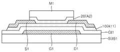
도 1을 참조하면, 기판(SUB1) 상에 제1 게이트(G1)가 구비될 수 있다. 기판(SUB1)은 유리 기판일 수 있지만, 그 밖의 다른 기판, 예컨대, 플라스틱 기판이나 실리콘 기판 등 통상의 반도체소자 공정에서 사용되는 다양한 기판 중 어느 하나일 수 있다. 제1 게이트(G1)는 일반적인 전극 물질(금속, 도전성 산화물 등)로 형성될 수 있다. 기판(SUB1) 상에 제1 게이트(G1)를 덮는 제1 게이트절연층(GI1)이 구비될 수 있다. 제1 게이트절연층(GI1)은 실리콘 산화물층, 실리콘 질산화물층 또는 실리콘 질화물층을 포함할 수 있으나, 그 밖의 다른 물질층, 예컨대, 실리콘 질화물층보다 유전상수가 큰 고유전물질층을 포함할 수도 있다. 게이트절연층(GI1)은 단층 또는 다층 구조를 가질 수 있다.Referring to FIG. 1, a first gate G1 may be provided on a substrate SUB1. The substrate SUB1 may be a glass substrate, but may be any of other substrates such as a plastic substrate or a silicon substrate and various substrates used in a general semiconductor device process. The first gate G1 may be formed of a common electrode material (metal, conductive oxide, etc.). A first gate insulating layer GI1 may be provided on the substrate SUB1 to cover the first gate G1. The first gate insulating layer GI1 may comprise a silicon oxide layer, a silicon oxynitride layer or a silicon nitride layer, but may also include other material layers, for example, a layer of high dielectric constant material having a higher dielectric constant than a silicon nitride layer have. The gate insulating layer GI1 may have a single-layer structure or a multi-layer structure.
제1 게이트절연층(GI1) 상에 제1 액티브층(A1)이 구비될 수 있다. 제1 액티브층(A1)은 제1 게이트(G1) 위쪽에 위치할 수 있다. 제1 액티브층(A1)의 X축 방향 폭은 제1 게이트(G1)의 X축 방향 폭보다 다소 작을 수 있지만, 제1 게이트(G1)와 유사하거나 그보다 큰 폭을 가질 수도 있다. 제1 액티브층(A1)은 산화물 반도체로 형성될 수 있다. 예컨대, 제1 액티브층(A1)은 ZnO 계열의 산화물 반도체를 포함할 수 있다. 이 경우, 상기 ZnO 계열의 산화물 반도체는 In, Ga 및 Al과 같은 13족 원소, Sn 및 Si와 같은 14족 원소, Zr, Hf 및 Ti와 같은 4족 원소(전이금속), Mg와 같은 2족 원소, Y 및 La과 같은 3족 원소(전이금속), Cu와 같은 11족 원소(전이금속), 그리고, Ta, Cr 등 그 밖의 전이금속으로 구성된 그룹에서 선택된 적어도 하나의 원소를 더 포함할 수 있다. 제1 액티브층(A1)은 비산화물 반도체로 형성될 수도 있다. 상기 비산화물 반도체는, 예컨대, 3족, 4족, 5족, 6족 원소 중 적어도 하나를 포함하는 반도체 또는 그 화합물일 수 있다. 구체적인 예로, 상기 비산화물 반도체는 Si, Ge, C, SiGe, GaN, GaAs, InSb, InP, CdS 등일 수 있다. 또한 상기 비산화물 반도체는 유기물 반도체이거나, 그래핀(graphene) 또는 CNT(carbon nanotube)일 수도 있다. 그러나 여기서 언급한 반도체 물질들은 예시적인 것이고, 그 밖에 다른 다양한 반도체 물질을 제1 액티브층(A1) 물질로 적용할 수 있다. 제1 액티브층(A1)은 단층 또는 다층 구조를 가질 수 있다.The first active layer A1 may be provided on the first gate insulating layer GI1. The first active layer A1 may be located above the first gate G1. The width in the X-axis direction of the first active layer A1 may be slightly smaller than the width in the X-axis direction of the first gate G1, but may have a width similar to or larger than that of the first gate G1. The first active layer A1 may be formed of an oxide semiconductor. For example, the first active layer A1 may include a ZnO-based oxide semiconductor. In this case, the ZnO-based oxide semiconductor may be a Group 13 element such as In, Ga and Al, a Group 14 element such as Sn and Si, a Group 4 element (transition metal) such as Zr, Hf and Ti, May further include at least one element selected from the group consisting of Group III elements (transition metals) such as elements Y and La, Group 11 elements (transition metals) such as Cu, and other transition metals such as Ta and Cr have. The first active layer Al may be formed of a non-oxide semiconductor. The non-oxide semiconductor may be a semiconductor or a compound containing at least one of Group 3, Group 4, Group 5, and Group 6 elements. As a specific example, the non-oxide semiconductor may be Si, Ge, C, SiGe, GaN, GaAs, InSb, InP, CdS, or the like. The non-oxide semiconductor may be an organic semiconductor, a graphene or a carbon nanotube (CNT). However, the semiconductor materials referred to herein are exemplary and a variety of other semiconductor materials can be applied as the first active layer (A1) material. The first active layer Al may have a single layer or a multilayer structure.
제1 게이트절연층(GI1) 상에 제1 액티브층(A1)의 양단에 각각 접촉되는 소오스전극(S1) 및 드레인전극(D1)이 구비될 수 있다. 소오스전극(S1) 및 드레인전극(D1)은 각각 제1 액티브층(A1)의 일단 및 타단을 커버할 수 있다. 소오스전극(S1) 및 드레인전극(D1)은 제1 게이트(G1)와 동일한 물질층일 수 있으나, 다른 물질층일 수도 있다. 소오스전극(S1) 및 드레인전극(D1)은 단일층 또는 다중층일 수 있다.A source electrode S1 and a drain electrode D1 which are in contact with both ends of the first active layer A1 may be provided on the first gate insulating layer GI1. The source electrode S1 and the drain electrode D1 may cover one end and the other end of the first active layer A1, respectively. The source electrode S1 and the drain electrode D1 may be the same material layer as the first gate G1, but they may be different material layers. The source electrode S1 and the drain electrode D1 may be a single layer or a multilayer.
제1 액티브층(A1) 상에 제2 액티브층(A2)이 구비될 수 있다. 제2 액티브층(A2)은 소오스전극(S1) 및 드레인전극(D1) 위로 연장되어 있을 수 있다. 즉, 제2 액티브층(A2)은 제1 액티브층(A1)에 접촉하면서 소오스전극(S1) 및 드레인전극(D1)의 적어도 일부를 커버하는 구조를 가질 수 있다. 따라서, 소오스전극(S1)의 일단 및 드레인전극(D1)의 일단은 제1 및 제2 액티브층(A1, A2) 사이에 배치될 수 있다. 제2 액티브층(A2)은, 제1 액티브층(A1)과 유사하게, 산화물 반도체 또는 비산화물 반도체로 형성될 수 있다. 상기 산화물 반도체와 비산화물 반도체의 구체적인 물질은 제1 액티브층(A1)에 대해서 예시한 물질과 유사할 수 있다. 제1 및 제2 액티브층(A1, A2)은 같은 물질로 형성될 수 있지만, 그렇지 않을 수도 있다. 제1 및 제2 액티브층(A1, A2)이 모두 산화물 반도체(또는 비산화물 반도체)로 형성되는 경우, 이들(A1, A2)은 동일 계열의 산화물 반도체(또는 비산화물 반도체)로 형성되거나 서로 다른 계열의 산화물 반도체(또는 비산화물 반도체)로 형성될 수 있다. 제1 및 제2 액티브층(A1, A2)이 동일 계열의 산화물 반도체(또는 비산화물 반도체)로 형성되는 경우, 이들(A1, A2)은 동일한 조성비를 가질 수 있지만, 서로 다른 조성비를 가질 수도 있다. 또한 제1 및 제2 액티브층(A1, A2) 중 하나는 산화물 반도체로 형성되고, 다른 하나는 비산화물 반도체로 형성될 수도 있다. 제1 및 제2 액티브층(A1, A2)을 서로 다른 물질(또는 서로 다른 조성비를 갖는 물질)로 형성하는 경우, 이들의 전기적 특성은 서로 다를 수 있다. 제1 및 제2 액티브층(A1, A2)의 두께는 동일할 수 있으나, 서로 다를 수도 있다. 또한 제1 및 제2 액티브층(A1, A2) 각각은 단층 또는 다층 구조를 가질 수 있다.A second active layer A2 may be provided on the first active layer A1. The second active layer A2 may extend over the source electrode S1 and the drain electrode D1. That is, the second active layer A2 may have a structure covering at least a part of the source electrode S1 and the drain electrode D1 while being in contact with the first active layer A1. Therefore, one end of the source electrode S1 and one end of the drain electrode D1 can be disposed between the first and second active layers A1 and A2. The second active layer A2 may be formed of an oxide semiconductor or a non-oxide semiconductor similarly to the first active layer A1. The specific materials of the oxide semiconductor and the non-oxide semiconductor may be similar to those exemplified for the first active layer (A1). The first and second active layers A1 and A2 may be formed of the same material, but may not. When both the first and second active layers A1 and A2 are formed of an oxide semiconductor (or a non-oxide semiconductor), these (A1 and A2) may be formed of oxide semiconductors (or non-oxide semiconductors) Oxide semiconductor (or non-oxide semiconductor). When the first and second active layers A1 and A2 are formed of the same series oxide semiconductor (or non-oxide semiconductor), these (A1 and A2) may have the same composition ratios but may have different composition ratios . Further, one of the first and second active layers A1 and A2 may be formed of an oxide semiconductor and the other may be formed of a non-oxide semiconductor. When the first and second active layers A1 and A2 are formed of different materials (or materials having different composition ratios), their electrical characteristics may be different from each other. The thicknesses of the first and second active layers A1 and A2 may be the same, but may be different from each other. Also, each of the first and second active layers A1 and A2 may have a single layer or a multilayer structure.
제1 게이트절연층(GI1) 상에 제2 액티브층(A2), 소오스전극(S1) 및 드레인전극(D1)을 덮는 제2 게이트절연층(GI2)이 구비될 수 있다. 제2 게이트절연층(GI2)은 제1 액티브층(A1), 제2 액티브층(A2), 소오스전극(S1) 및 드레인전극(D1)을 보호하는 보호층(passivation layer)의 역할도 할 수 있다. 제2 게이트절연층(GI2)은, 제1 게이트절연층(GI1)과 유사하게, 실리콘 산화물층, 실리콘 질산화물층 또는 실리콘 질화물층을 포함하거나, 그 밖의 다른 물질층, 예컨대, 실리콘 질화물층보다 유전상수가 큰 고유전물질층을 포함할 수 있다. 또한 제2 게이트절연층(GI2)은 단층 또는 다층 구조를 가질 수 있다. 제2 게이트절연층(GI2) 상에 제2 게이트(G2)가 구비될 수 있다. 제2 게이트(G2)는 일반적인 전극 물질(금속, 도전성 산화물 등)로 형성될 수 있다. 제2 게이트(G2)의 X축 방향 폭은 제2 액티브층(A2)의 X축 방향 폭보다 다소 클 수 있지만, 제2 액티브층(A2)과 유사하거나 그보다 작은 폭을 가질 수도 있다.A second gate insulating layer GI2 covering the second active layer A2, the source electrode S1 and the drain electrode D1 may be provided on the first gate insulating layer GI1. The second gate insulating layer GI2 may serve as a passivation layer for protecting the first active layer A1, the second active layer A2, the source electrode S1 and the drain electrode D1. have. The second gate insulating layer GI2 may include a silicon oxide layer, a silicon oxynitride layer, or a silicon nitride layer, similar to the first gate insulating layer GI1, or may include a silicon oxide layer, And may include a high-k material layer having a large constant. The second gate insulating layer GI2 may have a single layer or a multilayer structure. And a second gate G2 may be provided on the second gate insulating layer GI2. The second gate G2 may be formed of a general electrode material (metal, conductive oxide, or the like). The width in the X-axis direction of the second gate G2 may be slightly larger than the width in the X-axis direction of the second active layer A2, but may have a width similar to or smaller than that of the second active layer A2.
도 1의 트랜지스터의 평면 구조는 도 2와 같을 수 있다. 도 2에 도시된 평면 구조는 예시적인 것이고, 이 구조는 다양하게 변형될 수 있다.The planar structure of the transistor of Fig. 1 may be the same as that of Fig. The planar structure shown in Fig. 2 is an example, and this structure can be variously modified.
도 1과 같이 두 개의 액티브층(A1, A2)과 두 개의 게이트(G1, G2)를 포함하고, 소오스전극(S1) 및 드레인전극(D1)의 적어도 일부가 제1 및 제2 액티브층(A1, A2) 사이로 삽입된 트랜지스터는 우수한 동작 특성 및 성능을 가질 수 있다. 보다 상세히 설명하면, 도 1과 같은 트랜지스터에서는 두 개의 액티브층(A1, A2)이 소오스전극(S1) 및 드레인전극(D1)의 하면 및 상면에 접촉되어 있으므로, 이들 사이의 콘택 면적이 증가하고, 소오스전극(S1) 및 드레인전극(D1) 사이의 전류량(또는 전류 밀도)가 증가할 수 있다. 또한, 도 1과 같은 구조에서는 제1 게이트(G1)로 제1 액티브층(A1)의 전기적 특성을, 제2 게이트(G2)로 제2 액티브층(A2)의 전기적 특성을 독립적으로 제어할 수 있다. 제1 게이트(G1)와 제1 액티브층(A1) 사이에 소오스전극(S1) 및 드레인전극(D1)이 존재하지 않고, 제2 게이트(G2)와 제2 액티브층(A2) 사이에도 소오스전극(S1) 및 드레인전극(D1)이 존재하지 않기 때문에, 각각의 게이트(G1, G2)로 그에 대응하는 액티브층(A1, A2)의 특성을 제어하는 것이 용이할 수 있다. 만약 소오스전극(S1) 및 드레인전극(D1)의 일부가 제2 게이트(G2)와 제2 액티브층(A2) 사이를 가리고 있다면, 이로 인해, 제2 게이트(G2)에 의한 제2 액티브층(A2)의 특성 제어가 방해받을 수 있다. 그러나 본 실시예에서는 소오스전극(S1) 및 드레인전극(D1)이 제1 게이트(G1)와 제1 액티브층(A1) 사이 및 제2 게이트(G2)와 제2 액티브층(A2) 사이를 가리지 않으므로, 제1 및 제2 액티브층(A1, A2)의 특성을 용이하게 그리고 독립적으로 제어할 수 있다. 그러므로 트랜지스터의 동작 특성이 향상될 수 있고, 구동방법의 자유도가 증가할 수 있다.And at least a part of the source electrode S1 and the drain electrode D1 are formed in the first active layer A1 and the second active layer A1 as shown in FIG. 1, including two active layers A1 and A2 and two gates G1 and G2. 0.0 > A2, < / RTI > can have excellent operating characteristics and performance. More specifically, in the transistor shown in FIG. 1, since the two active layers A1 and A2 are in contact with the lower surface and the upper surface of the source electrode S1 and the drain electrode D1, the contact area therebetween increases, The current amount (or the current density) between the source electrode S1 and the drain electrode D1 may increase. 1, the electrical characteristics of the first active layer A1 can be controlled by the first gate G1 and the electrical characteristics of the second active layer A2 can be independently controlled by the second gate G2. have. The source electrode S1 and the drain electrode D1 do not exist between the first gate G1 and the first active layer A1 and also between the second gate G2 and the second active layer A2, It is easy to control the characteristics of the active layers A1 and A2 corresponding to the respective gates G1 and G2 because the gate electrode S1 and the drain electrode D1 do not exist. If a part of the source electrode S1 and the drain electrode D1 covers the gap between the second gate G2 and the second active layer A2, the second active layer A2) may be interrupted. However, in this embodiment, the source electrode S1 and the drain electrode D1 are provided between the first gate G1 and the first active layer A1 and between the second gate G2 and the second active layer A2, It is possible to easily and independently control the characteristics of the first and second active layers A1 and A2. Therefore, the operational characteristics of the transistor can be improved, and the degree of freedom of the driving method can be increased.
도 3은 본 발명의 실시예와 비교되는 비교예에 따른 트랜지스터를 보여주는 단면도이다.3 is a cross-sectional view showing a transistor according to a comparative example compared with the embodiment of the present invention.
도 3을 참조하면, 비교예에 따른 트랜지스터에서는 제1 및 제2 액티브층(A1', A2')이 전체적으로 서로 접합되어 있고, 소오스전극(S1') 및 드레인전극(D1')이 제2 액티브층(A2')의 상면으로 연장된 구조를 갖는다. 이러한 구조에서는 소오스전극(S1') 및 드레인전극(D1') 각각의 일부가 제2 게이트(G2')와 제2 액티브층(A2') 사이를 가리고 있기 때문에, 제2 게이트(G2')에 의한 제2 액티브층(A2')의 특성 제어가 방해를 받을 수 있다. 따라서 제1 및 제2 액티브층(A1', A2')의 특성은 주로 제1 게이트(G1')에 의해 제어되고, 제2 게이트(G2')는 보조적인 역할만 수행할 수 있다. 또한 소오스/드레인전극(S1', D1')과 액티브층(A1', A2') 사이의 콘택 면적이 작기 때문에, 소오스전극(S1')과 드레인전극(D1') 사이의 전류량(또는 전류 밀도)가 도 1의 트랜지스터의 그것보다 낮을 수 있다. 도 3에서 미설명된 참조번호 SUB1', GI1' 및 GI2' 는 각각 기판, 제1 게이트절연층 및 제2 게이트절연층을 나타낸다.Referring to FIG. 3, in the transistor according to the comparative example, the first and second active layers A1 'and A2' are entirely bonded together, and the source electrode S1 'and the drain electrode D1' And has a structure extending to the upper surface of the layer A2 '. In this structure, since part of each of the source electrode S1 'and the drain electrode D1' covers the gap between the second gate G2 'and the second active layer A2', the second gate G2 ' The characteristic control of the second active layer A2 'by the second active layer A2' may be disturbed. Therefore, the characteristics of the first and second active layers A1 'and A2' are mainly controlled by the first gate G1 ', and the second gate G2' can perform only an auxiliary role. (Or current density) between the source electrode S1 'and the drain electrode D1' because the contact area between the source / drain electrodes S1 'and D1' and the active layers A1 'and A2' May be lower than that of the transistor of FIG. Reference numerals SUB1 ', GI1' and GI2 ', which are not shown in Fig. 3, indicate a substrate, a first gate insulating layer and a second gate insulating layer, respectively.
도 4는 본 발명의 다른 실시예에 따른 트랜지스터를 보여주는 단면도이다.4 is a cross-sectional view illustrating a transistor according to another embodiment of the present invention.
도 4를 참조하면, 제1 액티브층(A11)이 소오스전극(S1) 및 드레인전극(D1)의 하면을 전체적으로 커버하도록 연장될 수 있다. 이때, 제1 액티브층(A11)에서 유효한(effective) 채널영역은 도 1의 제1 액티브층(A1)의 전체 영역과 유사할 수 있다. 즉, 제1 액티브층(A11)에서 소오스/드레인전극(S1, D1) 사이에 배치된 영역(중앙부)이 유효 채널영역일 수 있다. 도 4에서 제1 액티브층(A11)을 제외한 나머지 구성요소는 도 1의 그것과 동일(혹은, 유사)할 수 있다.Referring to FIG. 4, the first active layer A11 may extend to cover the entire lower surface of the source electrode S1 and the drain electrode D1. At this time, the effective channel region in the first active layer A11 may be similar to the entire region of the first active layer A1 in Fig. That is, the region (central portion) disposed between the source / drain electrodes S1 and D1 in the first active layer A11 may be an effective channel region. In FIG. 4, the remaining components except for the first active layer A11 may be the same as (or similar to) those of FIG.
도 4에서 제1 액티브층(A11)의 평면 구조는 제2 액티브층(A2), 소오스전극(S1) 및 드레인전극(D1)을 합한 구조의 평면 구조와 동일하거나 유사할 수 있다. 즉, 제1 액티브층(A11)의 평면 구조는 도 5와 같을 수 있다. 도 5의 평면 구조는 도 2에서 제2 액티브층(A2), 소오스전극(S1) 및 드레인전극(D1)을 합한 구조의 평면 구조와 동일하다. 이는 도 4의 제1 액티브층(A11)을 형성하는 제조공정과 관련된다. 이에 대해서는 추후에 상세히 설명한다.4, the planar structure of the first active layer A11 may be the same as or similar to the planar structure of the structure including the second active layer A2, the source electrode S1, and the drain electrode D1. That is, the planar structure of the first active layer A11 may be the same as that of FIG. The planar structure of FIG. 5 is the same as the planar structure of the structure in which the second active layer A2, the source electrode S1, and the drain electrode D1 are combined in FIG. This relates to the manufacturing process for forming the first active layer A11 of Fig. This will be described later in detail.
도 4 및 도 5에서는 제1 액티브층(A11)이 소오스전극(S1) 및 드레인전극(D1)의 하면을 전체적으로 커버하도록 확장된 구조에 대해 설명하였지만, 제1 액티브층(A11)과 유사하게 제2 액티브층(A2)도 확장된 구조를 가질 수 있다. 즉, 제2 액티브층(A2)은 소오스전극(S1) 및 드레인전극(D1)의 상면을 전체적으로 커버하도록 확장된 구조를 가질 수 있다.4 and 5, the structure in which the first active layer A11 is extended to cover the entire lower surface of the source electrode S1 and the drain electrode D1 has been described. However, The two active layers A2 may also have an extended structure. That is, the second active layer A2 may have an extended structure to cover the upper surfaces of the source electrode S1 and the drain electrode D1 as a whole.
도 6 내지 도 10은 본 발명의 실시예에 따른 트랜지스터(도 1)의 동작방법을 보여주는 단면도이다.6 to 10 are cross-sectional views illustrating a method of operating a transistor (FIG. 1) according to an embodiment of the present invention.
도 6을 참조하면, 제1 게이트(G1)에 제1 턴-온 전압(VON1)을 인가할 수 있고, 제2 게이트(G2)에 제2 턴-온 전압(VON2)을 인가할 수 있다. 제1 턴-온 전압(VON1)에 의해 제1 액티브층(A1)에 채널이 형성될 수 있고, 제2 턴-온 전압(VON2)에 의해 제2 액티브층(A2)에 채널이 형성될 수 있다. 이때, 소오스전극(S1)과 드레인전극(D1) 사이에도 소정의 전압을 인가할 수 있다. 이 경우, 제1 및 제2 액티브층(A1, A2)을 통해 소오스전극(S1)로부터 드레인전극(D1)으로 소정의 전류가 흐를 수 있다. 본 실시예에서와 같이, 두 개의 액티브층(A1, A2)이 소오스전극(S1) 및 드레인전극(D1)의 하면 및 상면에 접촉되어 있는 경우, 이들 사이의 콘택 면적이 증가하여, 소오스전극(S1)에서 드레인전극(D1)으로 흐르는 전류의 양(혹은, 밀도)가 증가할 수 있다. 상기 제1 턴-온 전압(VON1)과 제2 턴-온 전압(VON2)은 동일할 수도 있지만, 서로 다를 수도 있다. 예컨대, 제1 및 제2 액티브층(A1, A2)의 물질/특성/두께 등이 다를 경우, 이들을 활성화하는데, 즉, 이들 내에 채널을 형성하는데 필요한 전압(게이트전압)의 세기는 서로 다를 수 있다. 또한, 필요에 따라서는, 두 액티브층(A1, A2)의 물질이 동일한 경우라도, 의도적으로 두 게이트(G1, G2)에 인가하는 턴-온 전압(VON1, VON2)을 서로 다르게 할 수 있다.Referring to FIG. 6, a first turn-on
도 7을 참조하면, 제1 게이트(G1)에 제1 턴-오프 전압(VOFF1)을 인가할 수 있고, 제2 게이트(G2)에 제2 턴-오프 전압(VOFF2)을 인가할 수 있다. 이 경우, 소오스전극(S1)과 드레인전극(D1) 사이에 유효한 전류가 흐르지 않을 수 있다. 상기 제1 턴-오프 전압(VOFF1)과 제2 턴-오프 전압(VOFF2)은 동일할 수 있지만, 서로 다를 수도 있다.Referring to FIG. 7, a first turn-off
도 6 및 도 7은 두 게이트(G1, G2)에 동시에 턴-온 전압(VON1, VON2)을 인가하거나 턴-오프 전압(VOFF1, VOFF2)을 인가하는 경우에 대한 것이지만, 다른 실시예에서는, 두 게이트(G1, G2) 중 하나에는 턴-온 전압을 인가하고, 다른 하나에는 턴-오프 전압을 인가할 수 있다. 그 예가 도 8 및 도 9에 도시되어 있다.6 and 7 illustrate the case where the turn-on
도 8을 참조하면, 제1 게이트(G1)에 제1 턴-온 전압(VON1)을 인가할 수 있고, 제2 게이트(G2)에 제2 턴-오프 전압(VOFF2)을 인가할 수 있다. 이 경우, 제1 및 제2 액티브층(A1, A2) 중에서 제1 액티브층(A1)만 활성화될 수 있다. 즉, 제1 액티브층(A1)에만 채널이 형성될 수 있다. 따라서 소오스전극(S1)에서 제1 액티브층(A1)을 거쳐 드레인전극(D1)으로 전류가 흐를 수 있다.Referring to FIG. 8, a first turn-on
도 9를 참조하면, 제1 게이트(G1)에 제1 턴-오프 전압(VOFF1)을 인가할 수 있고, 제2 게이트(G2)에 제2 턴-온 전압(VON2)을 인가할 수 있다. 이 경우, 제1 및 제2 액티브층(A1, A2) 중에서 제2 액티브층(A2)에만 채널이 형성될 수 있다. 따라서 소오스전극(S1)에서 제2 액티브층(A2)을 거쳐 드레인전극(D1)으로 전류가 흐를 수 있다.Referring to FIG. 9, a first turn-off
도 6 내지 도 9의 실시예에서는 두 게이트(G1, G2)에 모두 전압을 인가하는 경우에 대해서 설명하였지만, 두 게이트(G1, G2) 중 하나에만 전압을 인가하고 다른 하나에는 전압을 인가하지 않을 수도 있다. 혹은, 두 게이트(G1, G2) 중 하나에만 전압을 인가하고, 다른 하나는 접지시킬 수도 있다. 이와 같이, 두 게이트(G1, G2) 중 하나에만 전압을 인가하는 경우, 상기 전압이 인가되는 게이트에 의해 두 액티브층(A1, A2) 중 적어도 하나의 전기적 특성이 제어될 수 있다. 예컨대, 제1 게이트(G1)에만 전압을 인가하는 경우, 제1 게이트(G1)에 가까운 제1 액티브층(A1)은 물론이고 제2 액티브층(A2)까지 제1 게이트(G1)에 의해 제어될 수 있다. 이와 유사하게, 제2 게이트(G2)에 의해 제2 액티브층(A2)과 제1 액티브층(A1)이 모두 제어될 수 있다.In the embodiments of FIGS. 6 to 9, the case of applying the voltage to both the gates G1 and G2 has been described. However, when the voltage is applied to only one of the two gates G1 and G2 and the voltage is not applied to the other It is possible. Alternatively, the voltage may be applied to only one of the two gates G1 and G2, and the other may be grounded. In this way, when a voltage is applied to only one of the two gates G1 and G2, the electrical characteristics of at least one of the two active layers A1 and A2 can be controlled by the gate to which the voltage is applied. For example, when a voltage is applied only to the first gate G1, control is performed by the first gate G1 not only to the first active layer A1 close to the first gate G1 but also to the second active layer A2 . Similarly, the second active layer A2 and the first active layer A1 can both be controlled by the second gate G2.
부가해서, 도 6 내지 도 9에서는 제1 게이트(G1)와 제2 게이트(G2)가 전기적으로 서로 분리되어 있는 경우에 대해서 설명하였지만, 본 발명의 다른 실시예에 따르면, 도 10에 도시된 바와 같이, 제1 게이트(G1)와 제2 게이트(G2)를 전기적으로 서로 연결할 수도 있다. 이 경우, 제1 게이트(G1)와 제2 게이트(G2)에 동시에 동일한 전압(V)을 인가할 수 있다.In addition, although FIGS. 6 to 9 illustrate the case where the first gate G1 and the second gate G2 are electrically separated from each other, according to another embodiment of the present invention, Similarly, the first gate G1 and the second gate G2 may be electrically connected to each other. In this case, the same voltage V can be simultaneously applied to the first gate G1 and the second gate G2.
도 6 내지 도 10에서는 도 1의 트랜지스터의 동작방법에 대해 설명하였지만, 본 동작방법은 도 4의 트랜지스터에도 동일하게 적용될 수 있다.Although the method of operation of the transistor of FIG. 1 has been described with reference to FIGS. 6 to 10, this method of operation may be similarly applied to the transistor of FIG.
도 11a 내지 도 11e는 본 발명의 실시예에 따른 트랜지스터의 제조방법을 보여준다. 도 1과 도 11a 내지 도 11e에서 동일한 참조번호는 동일한 구성요소를 나타낸다.11A to 11E show a method of manufacturing a transistor according to an embodiment of the present invention. Like reference numerals in FIG. 1 and FIGS. 11A to 11E denote like elements.
도 11a를 참조하면, 기판(SUB1) 상에 제1 게이트(G1)를 형성할 수 있다. 기판(SUB1)은 유리 기판일 수 있지만, 그 밖의 다른 기판, 예컨대, 플라스틱 기판이나 실리콘 기판 등 통상의 반도체소자 공정에서 사용되는 다양한 기판 중 어느 하나일 수 있다. 제1 게이트(G1)는 일반적인 전극 물질(금속, 도전성 산화물 등)로 형성할 수 있다. 다음, 제1 게이트(G1)를 덮는 제1 게이트절연층(GI1)을 형성할 수 있다. 제1 게이트절연층(GI1)은 실리콘 산화물, 실리콘 질산화물 또는 실리콘 질화물로 형성하거나, 그 밖의 다른 물질, 예컨대, 실리콘 질화물보다 유전상수가 큰 고유전물질로 형성할 수도 있다. 제1 게이트절연층(GI1)은 단층 또는 다층 구조로 형성할 수 있다. 이어서, 제1 게이트절연층(GI1) 상에 제1 반도체층(10)을 형성할 수 있다. 제1 반도체층(10)은 산화물 반도체 또는 비산화물 반도체로 형성할 수 있다.Referring to FIG. 11A, a first gate G1 may be formed on the substrate SUB1. The substrate SUB1 may be a glass substrate, but may be any of other substrates such as a plastic substrate or a silicon substrate and various substrates used in a general semiconductor device process. The first gate G1 may be formed of a general electrode material (metal, conductive oxide, or the like). Next, a first gate insulating layer GI1 covering the first gate G1 can be formed. The first gate insulating layer GI1 may be formed of silicon oxide, silicon oxynitride, or silicon nitride, or may be formed of a high dielectric constant material having a dielectric constant higher than that of other materials such as silicon nitride. The first gate insulating layer GI1 may be formed as a single layer or a multilayer structure. Next, the
도 11b를 참조하면, 제1 반도체층(10)을 패터닝할 수 있다. 패터닝된 제1 반도체층(10)은 제1 액티브층(A1)이라 할 수 있다. 이하에서는, 패터닝된 제1 반도체층(10)을 제1 액티브층(A1)이라 한다.Referring to FIG. 11B, the
도 11c를 참조하면, 제1 게이트절연층(GI1) 상에 제1 액티브층(A1)의 양단에 각각 접촉되는 소오스전극(S1) 및 드레인전극(D1)을 형성할 수 있다. 소오스전극(S1) 및 드레인전극(D1)은 각각 제1 액티브층(A1)의 일단 및 타단을 커버할 수 있다. 소오스전극(S1) 및 드레인전극(D1)은 제1 게이트(G1)와 동일한 물질층일 수 있으나, 다른 물질층일 수도 있다. 소오스전극(S1) 및 드레인전극(D1)은 단일 구조 또는 다중 구조로 형성할 수 있다. 다음, 제1 게이트절연층(GI1) 상에 제1 액티브층(A1), 소오스전극(S1) 및 드레인전극(D1)을 덮는 제2 반도체층(20)을 형성할 수 있다. 제2 반도체층(20)은 산화물 반도체 또는 비산화물 반도체로 형성할 수 있다.Referring to FIG. 11C, a source electrode S1 and a drain electrode D1, which are in contact with both ends of the first active layer A1, may be formed on the first gate insulating layer GI1. The source electrode S1 and the drain electrode D1 may cover one end and the other end of the first active layer A1, respectively. The source electrode S1 and the drain electrode D1 may be the same material layer as the first gate G1, but they may be different material layers. The source electrode S1 and the drain electrode D1 can be formed in a single structure or a multiple structure. Next, the
도 11d를 참조하면, 제2 반도체층(20)을 패터닝할 수 있다. 패터닝된 제2 반도체층(20)은 제2 액티브층(A2)이라 할 수 있다. 이하에서는, 패터닝된 제2 반도체층(20)을 제2 액티브층(A2)이라 한다.Referring to FIG. 11D, the
도 11e를 참조하면, 제1 게이트절연층(GI1) 상에 제2 액티브층(A2), 소오스전극(S1) 및 드레인전극(D1)을 덮는 제2 게이트절연층(GI2)을 형성할 수 있다. 제2 게이트절연층(GI2)은, 제1 게이트절연층(GI1)과 유사하게, 실리콘 산화물, 실리콘 질산화물 또는 실리콘 질화물로 형성하거나, 그 밖의 다른 물질, 예컨대, 실리콘 질화물보다 유전상수가 큰 고유전물질로 형성할 수 있다. 또한 제2 게이트절연층(GI2)은 단층 또는 다층 구조로 형성할 수 있다. 다음, 제2 게이트절연층(GI2) 상에 제2 게이트(G2)를 형성할 수 있다. 제2 게이트(G2)는 일반적인 전극 물질(금속, 도전성 산화물 등)로 형성할 수 있고, 단층 또는 다층 구조를 가질 수 있다. 이와 같은 방법으로 형성된 트랜지스터는 소정 온도에서 어닐링(annealing) 될 수 있다.Referring to FIG. 11E, a second gate insulating layer GI2 covering the second active layer A2, the source electrode S1, and the drain electrode D1 may be formed on the first gate insulating layer GI1 . The second gate insulating layer GI2 may be formed of silicon oxide, silicon oxynitride, or silicon nitride, similar to the first gate insulating layer GI1, or may be formed of other materials, for example, And the like. The second gate insulating layer GI2 may be formed as a single layer or a multilayer structure. Next, the second gate G2 may be formed on the second gate insulating layer GI2. The second gate G2 may be formed of a general electrode material (metal, conductive oxide, or the like), and may have a single layer or a multilayer structure. The transistor formed in this way can be annealed at a predetermined temperature.
도 12a 내지 도 12d는 본 발명의 다른 실시예에 따른 트랜지스터의 제조방법을 보여준다.12A to 12D show a method of manufacturing a transistor according to another embodiment of the present invention.
도 12a를 참조하면, 도 11a와 유사하게 기판(SUB1) 상에 제1 게이트(G1), 제1 게이트절연층(GI1) 및 제1 반도체층(10)을 순차로 형성할 수 있다.Referring to FIG. 12A, a first gate G1, a first gate insulating layer GI1, and a
도 12b를 참조하면, 제1 반도체층(10) 상에 소오스전극(S1) 및 드레인전극(D1)을 형성할 수 있다. 다음, 제1 반도체층(10) 상에 소오스전극(S1) 및 드레인전극(D1)을 덮는 제2 반도체층(20)을 형성할 수 있다. 제2 반도체층(20) 상에 이를 패터닝하기 위한 마스크층(M1)을 형성할 수 있다.Referring to FIG. 12B, a source electrode S1 and a drain electrode D1 may be formed on the
도 12c를 참조하면, 마스크층(M1)을 식각 장벽으로 이용해서 제2 반도체층(20)을 식각(패터닝)하고, 이어서, 제1 반도체층(10)을 식각(패터닝)할 수 있다. 제1 반도체층(10)의 식각시(패터닝시), 마스크층(M1)과 소오스전극(S1) 및 드레인전극(D1)이 식각 장벽으로 이용될 수 있다. 이러한 방법으로 제2 반도체층(20) 및 제1 반도체층(10)을 한 번의 공정으로 패터닝할 수 있다. 패터닝된 제1 반도체층(10)은 제1 액티브층(A11)이라 할 수 있고, 패터닝된 제2 반도체층(20)은 제2 액티브층(A2)이라 할 수 있다. 제1 액티브층(A11)은, 예컨대, 도 5와 같은 평면 구조를 가질 수 있다.Referring to FIG. 12C, the
도 12d를 참조하면, 마스크층(M1)을 제거한 상태에서, 제1 게이트절연층(GI1) 상에 제2 액티브층(A2), 소오스전극(S1) 및 드레인전극(D1)을 덮는 제2 게이트절연층(GI2)을 형성할 수 있다. 제2 게이트절연층(GI2) 상에 제2 게이트(G2)를 형성할 수 있다. 이와 같은 방법으로 형성된 트랜지스터는 소정 온도에서 어닐링(annealing) 될 수 있다.12D, a second gate insulating layer GI2 is formed on the first gate insulating layer GI1 to cover the second active layer A2, the source electrode S1, and the drain electrode D1, with the mask layer M1 removed. The insulating layer GI2 can be formed. And the second gate G2 may be formed on the second gate insulating layer GI2. The transistor formed in this way can be annealed at a predetermined temperature.
도 12a 내지 도 12d에서와 같이, 제2 반도체층(20) 및 제1 반도체층(10)을 한 번의 공정으로 패터닝할 경우, 제조공정을 단순화할 수 있고, 제조비용을 절감할 수 있다. 따라서 하나의 액티브층(채널층)을 사용하는 종래의 트랜지스터를 제조하는 경우와 유사한 공정수 및 비용으로 본 실시예에 따른 트랜지스터를 제조할 수 있다.12A to 12D, when the
본 발명의 실시예에 따른 트랜지스터는 액정표시장치 및 유기발광표시장치 등과 같은 평판표시장치에 스위칭소자 또는 구동소자로 적용될 수 있다. 앞서 설명한 바와 같이, 본 발명의 실시예에 따른 트랜지스터는 우수한 동작 특성을 갖고, 구동 방식의 자유도가 높기 때문에, 이를 평판표시장치에 적용하면, 평판표시장치의 동작 특성 및 성능을 향상시킬 수 있다. 액정표시장치 및 유기발광표시장치 등의 구조는 잘 알려진바, 이들에 대한 자세한 설명은 생략한다. 본 발명의 실시예에 따른 트랜지스터는 평판표시장치뿐 아니라, 메모리소자 및 논리소자 등 다른 전자장치 분야에 다양한 용도로 적용될 수 있다.The transistor according to the embodiment of the present invention can be applied to a flat panel display device such as a liquid crystal display device and an organic light emitting display device as a switching device or a driving device. As described above, since the transistor according to the embodiment of the present invention has excellent operation characteristics and has a high degree of freedom in the driving method, when it is applied to the flat panel display device, the operating characteristics and performance of the flat panel display device can be improved. A liquid crystal display device, and an organic light emitting display device are well known, and a detailed description thereof will be omitted. The transistor according to the embodiment of the present invention can be applied to various fields of electronic devices such as a memory device and a logic device as well as a flat panel display device.
상기한 설명에서 많은 사항이 구체적으로 기재되어 있으나, 그들은 발명의 범위를 한정하는 것이라기보다, 구체적인 실시예의 예시로서 해석되어야 한다. 예들 들어, 본 발명이 속하는 기술 분야에서 통상의 지식을 가진 자라면, 도 1 및 도 4의 트랜지스터는 다양하게 변형될 수 있음을 알 수 있을 것이다. 구체적인 예로, 소오스전극(S1) 및 드레인전극(D1) 중 하나는 두 액티브층(A1, A2 또는 A11, A2) 사이로 삽입되지 않을 수도 있고, 두 액티브층(A1, A2 또는 A11, A2)의 중앙부는 서로 접촉되지 않을 수 있으며, 각각의 액티브층(A1, A2, A11)은 다층 구조를 가질 수 있다. 그리고 도 11a 내지 도 11e 및 도 12a 내지 도 12d의 제조방법도 다양하게 변화될 수 있다. 부가해서, 당업자라면 본 발명의 사상(idea)은 박막 트랜지스터가 아닌 다른 트랜지스터에도 적용될 수 있음을 알 수 있을 것이다. 때문에 본 발명의 범위는 설명된 실시예에 의하여 정하여 질 것이 아니고 특허 청구범위에 기재된 기술적 사상에 의해 정하여져야 한다.While many have been described in detail above, they should not be construed as limiting the scope of the invention, but rather as examples of specific embodiments. For example, those of ordinary skill in the art will appreciate that the transistors of FIGS. 1 and 4 can be variously modified. As a specific example, one of the source electrode S1 and the drain electrode D1 may not be inserted between the two active layers A1, A2 or A11, A2 and the center of the two active layers A1, A2 or A11, May not be in contact with each other, and each of the active layers A1, A2, and A11 may have a multi-layer structure. The manufacturing methods of FIGS. 11A to 11E and 12A to 12D may also be variously changed. In addition, those skilled in the art will appreciate that the idea of the present invention is applicable to transistors other than thin film transistors. Therefore, the scope of the present invention is not to be determined by the described embodiments but should be determined by the technical idea described in the claims.
Claims (24)
Translated fromKorean상기 제1 및 제2 액티브층 중 적어도 제1 액티브층의 전기적 특성을 제어하기 위한 제1 게이트;
상기 제1 및 제2 액티브층 중 적어도 제2 액티브층의 전기적 특성을 제어하기 위한 제2 게이트; 및
상기 제1 및 제2 액티브층에 접촉된 소오스 및 드레인;을 포함하고,
상기 제1 게이트 상에 상기 제1 액티브층이 구비되고, 상기 제1 액티브층의 영역들 상에 상기 소오스 및 드레인이 구비되고, 상기 소오스 및 드레인의 적어도 일부 상에 상기 제2 액티브층이 구비되고, 상기 제2 액티브층 상에 상기 제2 게이트가 구비되며,
상기 소오스와 드레인 사이의 상기 제1 및 제2 액티브층은 서로 접촉된 트랜지스터.First and second active layers comprising a channel region;
A first gate for controlling electrical characteristics of at least a first active layer of the first and second active layers;
A second gate for controlling electrical characteristics of at least a second active layer of the first and second active layers; And
And a source and a drain in contact with the first and second active layers,
Wherein the first active layer is provided on the first gate, the source and drain are provided on regions of the first active layer, the second active layer is provided on at least a portion of the source and drain The second gate is provided on the second active layer,
Wherein the first and second active layers between the source and the drain are in contact with each other.
상기 소오스 및 드레인의 적어도 일부는 상기 제1 및 제2 액티브층 사이에 구비된 트랜지스터.The method according to claim 1,
Wherein at least a portion of the source and the drain are provided between the first and second active layers.
상기 소오스의 일단은 상기 제1 및 제2 액티브층 사이에 구비되고,
상기 드레인의 일단은 상기 제1 및 제2 액티브층 사이에 구비된 트랜지스터.3. The method of claim 2,
One end of the source is provided between the first and second active layers,
And one end of the drain is provided between the first and second active layers.
상기 제1 및 제2 액티브층 중 적어도 하나는 산화물 반도체를 포함하는 트랜지스터.The method according to claim 1,
Wherein at least one of the first and second active layers comprises an oxide semiconductor.
상기 제1 및 제2 액티브층 중 적어도 하나는 비산화물 반도체를 포함하는 트랜지스터.The method according to claim 1,
Wherein at least one of the first and second active layers comprises a non-oxide semiconductor.
상기 제1 및 제2 액티브층 중 하나는 산화물 반도체를 포함하고,
상기 제1 및 제2 액티브층 중 다른 하나는 비산화물 반도체를 포함하는 트랜지스터.The method according to claim 1,
Wherein one of the first and second active layers comprises an oxide semiconductor,
And the other of the first and second active layers comprises a non-oxide semiconductor.
상기 제1 및 제2 액티브층은 상기 제1 및 제2 게이트 사이에 구비되고,
상기 제1 및 제2 액티브층 중 상기 제1 액티브층은 상기 제1 게이트에 가까이 배치되고, 상기 제2 액티브층은 상기 제2 게이트에 가까이 배치된 트랜지스터.The method according to claim 1,
Wherein the first and second active layers are provided between the first and second gates,
Wherein the first active layer of the first and second active layers is disposed near the first gate and the second active layer is disposed near the second gate.
상기 제1 및 제2 액티브층 중 적어도 하나는 상기 소오스 및 드레인 중 적어도 하나의 일면 전체를 커버하는 구조를 갖는 트랜지스터.The method according to claim 1,
Wherein at least one of the first and second active layers covers at least one surface of at least one of the source and the drain.
상기 제1 및 제2 게이트는 전기적으로 서로 연결된 트랜지스터.The method according to claim 1,
Wherein the first and second gates are electrically connected to each other.
상기 제1 및 제2 게이트는 전기적으로 서로 분리된 트랜지스터.The method according to claim 1,
Wherein the first and second gates are electrically isolated from each other.
상기 제1 및 제2 게이트 중 적어도 하나에 전압을 인가하는 단계;를 포함하는 트랜지스터의 동작방법.The method for operating a transistor according to claim 1,
And applying a voltage to at least one of the first and second gates.
상기 제1 및 제2 게이트에 동일한 전압을 인가하는 트랜지스터의 동작방법.13. The method of claim 12,
And applying the same voltage to the first and second gates.
상기 제1 및 제2 게이트에 서로 다른 전압을 인가하는 트랜지스터의 동작방법.13. The method of claim 12,
And applying different voltages to the first and second gates.
상기 제1 및 제2 게이트에 턴-온(turn-on) 전압 또는 턴-오프(turn-off) 전압을 인가하는 트랜지스터의 동작방법.13. The method of claim 12,
And applying a turn-on voltage or a turn-off voltage to the first and second gates.
상기 제1 및 제2 게이트 중 하나에 턴-온(turn-on) 전압을 인가하고,
상기 제1 및 제2 게이트 중 다른 하나에 턴-오프(turn-off) 전압을 인가하는 트랜지스터의 동작방법.13. The method of claim 12,
Applying a turn-on voltage to one of the first and second gates,
And applying a turn-off voltage to the other of the first and second gates.
상기 전자장치는 평판표시장치인 전자장치.18. The method of claim 17,
Wherein the electronic device is a flat panel display.
상기 제1 게이트를 덮는 제1 게이트절연층을 형성하는 단계;
상기 제1 게이트절연층 상에 제1 액티브층을 형성하는 단계;
상기 제1 액티브층의 제1 및 제2 영역에 각각 접촉된 소오스 및 드레인을 형성하는 단계;
상기 제1 액티브층 상에 상기 소오스 및 드레인의 적어도 일부를 덮는 제2 액티브층을 형성하는 단계;
상기 제2 액티브층을 덮는 제2 게이트절연층을 형성하는 단계; 및
상기 제2 게이트절연층 상에 제2 게이트를 형성하는 단계;를 포함하고,
상기 소오스와 드레인 사이의 상기 제1 및 제2 액티브층은 서로 접촉되도록 형성되는 트랜지스터의 제조방법.Forming a first gate;
Forming a first gate insulating layer covering the first gate;
Forming a first active layer on the first gate insulating layer;
Forming a source and a drain in contact with the first and second regions of the first active layer, respectively;
Forming a second active layer over the first active layer to cover at least a portion of the source and drain;
Forming a second gate insulating layer over the second active layer; And
And forming a second gate on the second gate insulating layer,
Wherein the first and second active layers between the source and the drain are formed to be in contact with each other.
상기 제1 게이트절연층 상에 제1 반도체층을 형성하는 단계;
상기 제1 반도체층을 패터닝하여 상기 제1 액티브층을 형성하는 단계;
상기 제1 액티브층에 접촉된 상기 소오스 및 드레인을 형성하는 단계;
상기 제1 액티브층, 상기 소오스 및 상기 드레인을 덮는 제2 반도체층을 형성하는 단계; 및
상기 제2 반도체층을 패터닝하여 상기 제2 액티브층을 형성하는 단계;를 포함하는 트랜지스터의 제조방법.20. The method of claim 19,
Forming a first semiconductor layer on the first gate insulating layer;
Patterning the first semiconductor layer to form the first active layer;
Forming the source and drain in contact with the first active layer;
Forming a second semiconductor layer covering the first active layer, the source and the drain; And
And patterning the second semiconductor layer to form the second active layer.
상기 제1 게이트를 덮는 제1 게이트절연층을 형성하는 단계;
상기 제1 게이트절연층 상에 제1 반도체층을 형성하는 단계;
상기 제1 반도체층 상에 소오스 및 드레인을 형성하는 단계;
상기 제1 반도체층, 상기 소오스 및 상기 드레인을 덮는 제2 반도체층을 형성하는 단계;
상기 제2 반도체층 및 상기 제1 반도체층을 패터닝하여, 상기 제2 반도체층으로부터 제2 액티브층을 형성하고 상기 제1 반도체층으로부터 제1 액티브층을 형성하는 단계;
상기 제2 액티브층을 덮는 제2 게이트절연층을 형성하는 단계; 및
상기 제2 게이트절연층 상에 제2 게이트를 형성하는 단계;를 포함하고,
상기 소오스 및 드레인은 상기 제1 액티브층의 제1 및 제2 영역에 각각 접촉되고, 상기 제2 액티브층은 상기 소오스 및 드레인의 적어도 일부를 덮으며, 상기 소오스와 드레인 사이의 상기 제1 및 제2 액티브층은 서로 접촉되도록 형성되는 트랜지스터의 제조방법.Forming a first gate;
Forming a first gate insulating layer covering the first gate;
Forming a first semiconductor layer on the first gate insulating layer;
Forming a source and a drain on the first semiconductor layer;
Forming a second semiconductor layer covering the first semiconductor layer, the source and the drain;
Patterning the second semiconductor layer and the first semiconductor layer to form a second active layer from the second semiconductor layer and form a first active layer from the first semiconductor layer;
Forming a second gate insulating layer over the second active layer; And
And forming a second gate on the second gate insulating layer,
Wherein the source and drain are respectively in contact with the first and second regions of the first active layer and the second active layer covers at least a portion of the source and drain and the first and second regions between the source and drain, And the two active layers are formed to be in contact with each other.
상기 제1 및 제2 액티브층 중 적어도 하나는 산화물 반도체로 형성하는 트랜지스터의 제조방법.20. The method of claim 19,
Wherein at least one of the first and second active layers is formed of an oxide semiconductor.
상기 제1 및 제2 액티브층 중 적어도 하나는 비산화물 반도체로 형성하는 트랜지스터의 제조방법.20. The method of claim 19,
Wherein at least one of the first and second active layers is formed of a non-oxide semiconductor.
상기 제1 및 제2 액티브층 중 하나는 산화물 반도체로 형성하고,
상기 제1 및 제2 액티브층 중 다른 하나는 비산화물 반도체로 형성하는 트랜지스터의 제조방법.20. The method of claim 19,
Wherein one of the first and second active layers is formed of an oxide semiconductor,
And the other of the first and second active layers is formed of a non-oxide semiconductor.
Priority Applications (2)
| Application Number | Priority Date | Filing Date | Title |
|---|---|---|---|
| KR1020100126357AKR101680768B1 (en) | 2010-12-10 | 2010-12-10 | Transistor and electronic device including the same |
| US13/167,299US8779428B2 (en) | 2010-12-10 | 2011-06-23 | Transistors and electronic devices including the same |
Applications Claiming Priority (1)
| Application Number | Priority Date | Filing Date | Title |
|---|---|---|---|
| KR1020100126357AKR101680768B1 (en) | 2010-12-10 | 2010-12-10 | Transistor and electronic device including the same |
Publications (2)
| Publication Number | Publication Date |
|---|---|
| KR20120065048A KR20120065048A (en) | 2012-06-20 |
| KR101680768B1true KR101680768B1 (en) | 2016-11-29 |
Family
ID=46198745
Family Applications (1)
| Application Number | Title | Priority Date | Filing Date |
|---|---|---|---|
| KR1020100126357AActiveKR101680768B1 (en) | 2010-12-10 | 2010-12-10 | Transistor and electronic device including the same |
Country Status (2)
| Country | Link |
|---|---|
| US (1) | US8779428B2 (en) |
| KR (1) | KR101680768B1 (en) |
Cited By (1)
| Publication number | Priority date | Publication date | Assignee | Title |
|---|---|---|---|---|
| KR20220017960A (en)* | 2013-07-31 | 2022-02-14 | 가부시키가이샤 한도오따이 에네루기 켄큐쇼 | Semiconductor device |
Families Citing this family (93)
| Publication number | Priority date | Publication date | Assignee | Title |
|---|---|---|---|---|
| US9721825B2 (en) | 2008-12-02 | 2017-08-01 | Arizona Board Of Regents, A Body Corporate Of The State Of Arizona, Acting For And On Behalf Of Arizona State University | Method of providing a flexible semiconductor device and flexible semiconductor device thereof |
| WO2014039698A1 (en)* | 2012-09-07 | 2014-03-13 | Arizona Board Of Regents, A Body Corporate Of The State Of Arizona Acting For And On Behalf Of Arizona State University | Dual active layer semiconductor device and method of manufacturing the same |
| US9991311B2 (en) | 2008-12-02 | 2018-06-05 | Arizona Board Of Regents On Behalf Of Arizona State University | Dual active layer semiconductor device and method of manufacturing the same |
| US9601530B2 (en) | 2008-12-02 | 2017-03-21 | Arizona Board Of Regents, A Body Corporated Of The State Of Arizona, Acting For And On Behalf Of Arizona State University | Dual active layer semiconductor device and method of manufacturing the same |
| KR101362025B1 (en) | 2009-05-29 | 2014-02-13 | 아리조나 보드 오브 리젠츠 퍼 앤 온 비하프 오브 아리조나 스테이트 유니버시티 | Method of providing a flexible semiconductor device at high temperatures and flexible semiconductor device thereof |
| WO2012021196A2 (en) | 2010-05-21 | 2012-02-16 | Arizona Board Of Regents, For And On Behalf Of Arizona State University | Method for manufacturing electronic devices and electronic devices thereof |
| WO2012021197A2 (en) | 2010-05-21 | 2012-02-16 | Arizona Board Of Regents, For And On Behalf Of Arizona State University | Method of manufacturing electronic devices on both sides of a carrier substrate and electronic devices thereof |
| JP5306438B2 (en)* | 2011-11-14 | 2013-10-02 | シャープ株式会社 | Field effect transistor and manufacturing method thereof |
| US9048323B2 (en) | 2012-04-30 | 2015-06-02 | Semiconductor Energy Laboratory Co., Ltd. | Semiconductor device |
| TWI478344B (en)* | 2012-07-04 | 2015-03-21 | E Ink Holdings Inc | Transistor and manufacturing method thereof |
| WO2014021442A1 (en)* | 2012-08-03 | 2014-02-06 | Semiconductor Energy Laboratory Co., Ltd. | Oxide semiconductor stacked film and semiconductor device |
| JP6220597B2 (en)* | 2012-08-10 | 2017-10-25 | 株式会社半導体エネルギー研究所 | Semiconductor device |
| TWI799011B (en)* | 2012-09-14 | 2023-04-11 | 日商半導體能源研究所股份有限公司 | Semiconductor device and method for fabricating the same |
| TWI637517B (en) | 2012-10-24 | 2018-10-01 | 半導體能源研究所股份有限公司 | Semiconductor device and method of manufacturing same |
| TWI624949B (en) | 2012-11-30 | 2018-05-21 | 半導體能源研究所股份有限公司 | Semiconductor device |
| DE112013006219T5 (en) | 2012-12-25 | 2015-09-24 | Semiconductor Energy Laboratory Co., Ltd. | Semiconductor device and its manufacturing method |
| KR102853941B1 (en)* | 2012-12-28 | 2025-09-02 | 가부시키가이샤 한도오따이 에네루기 켄큐쇼 | Semiconductor device |
| US9391096B2 (en)* | 2013-01-18 | 2016-07-12 | Semiconductor Energy Laboratory Co., Ltd. | Semiconductor device and method for manufacturing the same |
| US9368636B2 (en)* | 2013-04-01 | 2016-06-14 | Semiconductor Energy Laboratory Co., Ltd. | Method for manufacturing a semiconductor device comprising a plurality of oxide semiconductor layers |
| CN103219463B (en)* | 2013-04-08 | 2015-09-02 | 上海和辉光电有限公司 | Organic electronic light emitting device and manufacture method thereof |
| US10304859B2 (en) | 2013-04-12 | 2019-05-28 | Semiconductor Energy Laboratory Co., Ltd. | Semiconductor device having an oxide film on an oxide semiconductor film |
| TWI620324B (en)* | 2013-04-12 | 2018-04-01 | 半導體能源研究所股份有限公司 | Semiconductor device |
| KR102210298B1 (en)* | 2013-05-09 | 2021-01-29 | 가부시키가이샤 한도오따이 에네루기 켄큐쇼 | Semiconductor device and manufacturing method thereof |
| TWI742574B (en)* | 2013-05-16 | 2021-10-11 | 日商半導體能源研究所股份有限公司 | Semiconductor device |
| KR102537022B1 (en) | 2013-05-20 | 2023-05-30 | 가부시키가이샤 한도오따이 에네루기 켄큐쇼 | Semiconductor device |
| CN109888022A (en)* | 2013-05-20 | 2019-06-14 | 株式会社半导体能源研究所 | semiconductor device |
| TWI664731B (en)* | 2013-05-20 | 2019-07-01 | 半導體能源研究所股份有限公司 | Semiconductor device |
| US9647125B2 (en)* | 2013-05-20 | 2017-05-09 | Semiconductor Energy Laboratory Co., Ltd. | Semiconductor device and method for manufacturing the same |
| DE102014019794B4 (en) | 2013-05-20 | 2024-10-24 | Semiconductor Energy Laboratory Co., Ltd. | semiconductor device |
| JP2015195327A (en)* | 2013-06-05 | 2015-11-05 | 株式会社半導体エネルギー研究所 | semiconductor device |
| JP6400336B2 (en) | 2013-06-05 | 2018-10-03 | 株式会社半導体エネルギー研究所 | Semiconductor device |
| TWI624936B (en) | 2013-06-05 | 2018-05-21 | 半導體能源研究所股份有限公司 | Display device |
| KR102282108B1 (en)* | 2013-06-13 | 2021-07-26 | 가부시키가이샤 한도오따이 에네루기 켄큐쇼 | Semiconductor device |
| US9035301B2 (en)* | 2013-06-19 | 2015-05-19 | Semiconductor Energy Laboratory Co., Ltd. | Imaging device |
| KR102522133B1 (en) | 2013-06-27 | 2023-04-17 | 가부시키가이샤 한도오따이 에네루기 켄큐쇼 | Semiconductor device |
| US9666697B2 (en)* | 2013-07-08 | 2017-05-30 | Semiconductor Energy Laboratory Co., Ltd. | Semiconductor device and method for manufacturing semiconductor device including an electron trap layer |
| US20150008428A1 (en) | 2013-07-08 | 2015-01-08 | Semiconductor Energy Laboratory Co., Ltd. | Semiconductor device and method for manufacturing semiconductor device |
| JP6322503B2 (en) | 2013-07-16 | 2018-05-09 | 株式会社半導体エネルギー研究所 | Semiconductor device |
| CN103474470A (en)* | 2013-08-20 | 2013-12-25 | 北京京东方光电科技有限公司 | Thin film transistor, array substrate and manufacturing method thereof, and display device |
| US9449853B2 (en)* | 2013-09-04 | 2016-09-20 | Semiconductor Energy Laboratory Co., Ltd. | Method for manufacturing semiconductor device comprising electron trap layer |
| JP6401977B2 (en)* | 2013-09-06 | 2018-10-10 | 株式会社半導体エネルギー研究所 | Semiconductor device |
| JP2015079946A (en) | 2013-09-13 | 2015-04-23 | 株式会社半導体エネルギー研究所 | Semiconductor device manufacturing method |
| US9461126B2 (en)* | 2013-09-13 | 2016-10-04 | Semiconductor Energy Laboratory Co., Ltd. | Transistor, clocked inverter circuit, sequential circuit, and semiconductor device including sequential circuit |
| TWI633668B (en) | 2013-09-23 | 2018-08-21 | 半導體能源研究所股份有限公司 | Semiconductor device |
| KR102258374B1 (en)* | 2013-10-18 | 2021-06-01 | 삼성디스플레이 주식회사 | Thin film transistor, display panel having the same and method of manufacturing the same |
| US9455349B2 (en) | 2013-10-22 | 2016-09-27 | Semiconductor Energy Laboratory Co., Ltd. | Oxide semiconductor thin film transistor with reduced impurity diffusion |
| TWI642186B (en)* | 2013-12-18 | 2018-11-21 | 日商半導體能源研究所股份有限公司 | Semiconductor device |
| US9401432B2 (en)* | 2014-01-16 | 2016-07-26 | Semiconductor Energy Laboratory Co., Ltd. | Semiconductor device and electronic device |
| WO2017034644A2 (en) | 2015-06-09 | 2017-03-02 | ARIZONA BOARD OF REGENTS a body corporate for THE STATE OF ARIZONA for and on behalf of ARIZONA STATE UNIVERSITY | Method of providing an electronic device and electronic device thereof |
| WO2015156891A2 (en) | 2014-01-23 | 2015-10-15 | Arizona Board Of Regents, Acting For And On Behalf Of Arizona State University | Method of providing a flexible semiconductor device and flexible semiconductor device thereof |
| US10381224B2 (en) | 2014-01-23 | 2019-08-13 | Arizona Board Of Regents On Behalf Of Arizona State University | Method of providing an electronic device and electronic device thereof |
| KR102306200B1 (en)* | 2014-01-24 | 2021-09-30 | 가부시키가이샤 한도오따이 에네루기 켄큐쇼 | Semiconductor device |
| WO2015130082A1 (en)* | 2014-02-25 | 2015-09-03 | 엘지디스플레이 주식회사 | Display backplane and method for manufacturing same |
| KR101672091B1 (en)* | 2014-02-25 | 2016-11-02 | 엘지디스플레이 주식회사 | Organic emitting display device having multi-type thin film transistor |
| US9595546B2 (en) | 2014-02-25 | 2017-03-14 | Lg Display Co., Ltd. | Display backplane and method of fabricating the same |
| US20150263140A1 (en)* | 2014-03-14 | 2015-09-17 | Semiconductor Energy Laboratory Co., Ltd. | Method for manufacturing semiconductor device |
| JP6537341B2 (en)* | 2014-05-07 | 2019-07-03 | 株式会社半導体エネルギー研究所 | Semiconductor device |
| JP2017518638A (en) | 2014-05-13 | 2017-07-06 | アリゾナ・ボード・オブ・リージェンツ・フォー・アンド・オン・ビハーフ・オブ・アリゾナ・ステイト・ユニバーシティArizona Board Of Regents For And On Behalf Of Arizona State University | Method for providing an electronic device and the electronic device |
| US9722090B2 (en)* | 2014-06-23 | 2017-08-01 | Semiconductor Energy Laboratory Co., Ltd. | Semiconductor device including first gate oxide semiconductor film, and second gate |
| US10559667B2 (en) | 2014-08-25 | 2020-02-11 | Semiconductor Energy Laboratory Co., Ltd. | Semiconductor device and method for measuring current of semiconductor device |
| CN104362179B (en)* | 2014-10-13 | 2017-04-26 | 京东方科技集团股份有限公司 | Thin-film transistor, manufacturing method of thin-film transistor, array substrate and display device |
| US9991393B2 (en)* | 2014-10-16 | 2018-06-05 | Semiconductor Energy Laboratory Co., Ltd. | Semiconductor device, module, and electronic device |
| WO2016073478A1 (en)* | 2014-11-04 | 2016-05-12 | Royole Corporation | Thin film transistor |
| US9768317B2 (en)* | 2014-12-08 | 2017-09-19 | Semiconductor Energy Laboratory Co., Ltd. | Semiconductor device, manufacturing method of semiconductor device, and electronic device |
| US9960283B2 (en) | 2014-12-09 | 2018-05-01 | Shenzhen China Star Optoelectronics Technology Co., Ltd | Thin-film transistor |
| CN104465785B (en)* | 2014-12-09 | 2019-02-12 | 深圳市华星光电技术有限公司 | thin film transistor |
| US10446582B2 (en) | 2014-12-22 | 2019-10-15 | Arizona Board Of Regents On Behalf Of Arizona State University | Method of providing an imaging system and imaging system thereof |
| US9741742B2 (en) | 2014-12-22 | 2017-08-22 | Arizona Board Of Regents, A Body Corporate Of The State Of Arizona, Acting For And On Behalf Of Arizona State University | Deformable electronic device and methods of providing and using deformable electronic device |
| CN105810744B (en)* | 2014-12-30 | 2019-10-25 | 昆山国显光电有限公司 | Thin film transistor and its manufacturing method |
| CN104966698B (en)* | 2015-07-16 | 2018-07-17 | 深圳市华星光电技术有限公司 | Array substrate, the manufacturing method of array substrate and display device |
| US10032921B2 (en)* | 2015-07-31 | 2018-07-24 | Semiconductor Energy Laboratory Co., Ltd. | Semiconductor device, display module, and electronic device |
| CN105742309B (en)* | 2016-02-29 | 2019-05-03 | 深圳市华星光电技术有限公司 | Complementary thin film transistor and method of making the same |
| JP6968567B2 (en)* | 2016-04-22 | 2021-11-17 | 株式会社半導体エネルギー研究所 | Manufacturing method of semiconductor device |
| KR102617379B1 (en) | 2016-05-02 | 2023-12-27 | 삼성디스플레이 주식회사 | Organic light emitting display apparatus and manufacturing method thereof |
| US9847428B1 (en)* | 2016-08-08 | 2017-12-19 | United Microelectronics Corp. | Oxide semiconductor device |
| CN106252362B (en)* | 2016-08-31 | 2019-07-12 | 深圳市华星光电技术有限公司 | A kind of array substrate and preparation method thereof |
| KR101842796B1 (en) | 2016-11-02 | 2018-03-28 | 경희대학교 산학협력단 | Oxide semiconductor transistor having dual gate structure and method of manufacturing the same |
| KR102597588B1 (en)* | 2016-11-23 | 2023-11-02 | 엘지디스플레이 주식회사 | Display device and degradation compensation method of the same |
| US10008614B1 (en)* | 2017-03-21 | 2018-06-26 | United Microelectronics Corp. | Dual channel transistor |
| CN107154407A (en)* | 2017-05-17 | 2017-09-12 | 厦门天马微电子有限公司 | Laminated film transistor device and its manufacture method, display panel and display device |
| KR102420080B1 (en)* | 2017-05-19 | 2022-07-13 | 삼성디스플레이 주식회사 | Multi-channel TFT and Pixel comprising the TFT |
| JP6844845B2 (en) | 2017-05-31 | 2021-03-17 | 三国電子有限会社 | Display device |
| JP7237944B2 (en)* | 2018-04-27 | 2023-03-13 | 株式会社半導体エネルギー研究所 | SEMICONDUCTOR DEVICE AND METHOD FOR MANUFACTURING SEMICONDUCTOR DEVICE |
| JP7190729B2 (en) | 2018-08-31 | 2022-12-16 | 三国電子有限会社 | ORGANIC ELECTROLUMINESCENT DEVICE HAVING CARRIER INJECTION CONTROL ELECTRODE |
| JP7246681B2 (en)* | 2018-09-26 | 2023-03-28 | 三国電子有限会社 | TRANSISTOR, TRANSISTOR MANUFACTURING METHOD, AND DISPLAY DEVICE INCLUDING TRANSISTOR |
| JP7190740B2 (en) | 2019-02-22 | 2022-12-16 | 三国電子有限会社 | Display device having an electroluminescence element |
| KR102749086B1 (en) | 2019-03-14 | 2025-01-03 | 삼성디스플레이 주식회사 | Display device |
| KR102198343B1 (en)* | 2019-05-31 | 2021-01-04 | 연세대학교 산학협력단 | Field effect light emission device |
| CN110364566B (en)* | 2019-07-19 | 2023-07-25 | 京东方科技集团股份有限公司 | Transistor, manufacturing method thereof, transistor device, display substrate and device |
| KR102756389B1 (en)* | 2019-12-24 | 2025-01-17 | 삼성디스플레이 주식회사 | Photo transistor and display device comprising of the same |
| JP7444436B2 (en) | 2020-02-05 | 2024-03-06 | 三国電子有限会社 | liquid crystal display device |
| GB2604025B (en) | 2020-12-29 | 2023-06-21 | Lg Display Co Ltd | Thin film transistor, method for manufacturing the thin film transistor and display device comprising the thin film transistor |
| US20230189565A1 (en)* | 2021-09-30 | 2023-06-15 | Boe Technology Group Co., Ltd. | Thin film transistor and method for manufacturing the same, display substrate, and display device |
Citations (1)
| Publication number | Priority date | Publication date | Assignee | Title |
|---|---|---|---|---|
| JP2010161382A (en)* | 2007-06-29 | 2010-07-22 | Semiconductor Energy Lab Co Ltd | Semiconductor device and manufacturing method of the same |
Family Cites Families (6)
| Publication number | Priority date | Publication date | Assignee | Title |
|---|---|---|---|---|
| JP2899078B2 (en) | 1990-07-10 | 1999-06-02 | 三菱製紙株式会社 | Support for photosensitive material |
| KR950003898A (en) | 1993-07-23 | 1995-02-17 | 이헌조 | Pixel Structure of TFT LCD Panel with Double Gate Structure |
| US5793072A (en)* | 1996-02-28 | 1998-08-11 | International Business Machines Corporation | Non-photosensitive, vertically redundant 2-channel α-Si:H thin film transistor |
| US20060068532A1 (en) | 2004-09-28 | 2006-03-30 | Sharp Laboratories Of America, Inc. | Dual-gate thin-film transistor |
| JP5152448B2 (en) | 2004-09-21 | 2013-02-27 | カシオ計算機株式会社 | Pixel drive circuit and image display device |
| US20060081936A1 (en) | 2004-09-28 | 2006-04-20 | Jae-Joon Kim | Semiconductor device for low power operation |
- 2010
- 2010-12-10KRKR1020100126357Apatent/KR101680768B1/enactiveActive
- 2011
- 2011-06-23USUS13/167,299patent/US8779428B2/enactiveActive
Patent Citations (1)
| Publication number | Priority date | Publication date | Assignee | Title |
|---|---|---|---|---|
| JP2010161382A (en)* | 2007-06-29 | 2010-07-22 | Semiconductor Energy Lab Co Ltd | Semiconductor device and manufacturing method of the same |
Cited By (2)
| Publication number | Priority date | Publication date | Assignee | Title |
|---|---|---|---|---|
| KR20220017960A (en)* | 2013-07-31 | 2022-02-14 | 가부시키가이샤 한도오따이 에네루기 켄큐쇼 | Semiconductor device |
| KR102419951B1 (en) | 2013-07-31 | 2022-07-11 | 가부시키가이샤 한도오따이 에네루기 켄큐쇼 | Semiconductor device |
Also Published As
| Publication number | Publication date |
|---|---|
| US20120146713A1 (en) | 2012-06-14 |
| KR20120065048A (en) | 2012-06-20 |
| US8779428B2 (en) | 2014-07-15 |
Similar Documents
| Publication | Publication Date | Title |
|---|---|---|
| KR101680768B1 (en) | Transistor and electronic device including the same | |
| JP5536328B2 (en) | Transistor and manufacturing method thereof | |
| EP2146379B1 (en) | Transistor comprising ZnO based channel layer | |
| KR101529575B1 (en) | Transistor, inverter comprising the same and methods of manufacturing transistor and inverter | |
| KR101522400B1 (en) | Inverter and logic device comprising the same | |
| KR101623956B1 (en) | Transistor, method of manufacturing the same and electronic device comprising transistor | |
| KR101791938B1 (en) | Graphene electronic device comprising a plurality of graphene channel layers | |
| JP5219369B2 (en) | Thin film transistor having ternary compound channel layer and manufacturing method thereof | |
| KR101922115B1 (en) | Field effect transistor having double transition metal dichalcogenide channel | |
| TWI363424B (en) | ||
| KR101851565B1 (en) | Transistor, method of manufacturing the same and electronic device comprising transistor | |
| KR102194235B1 (en) | Thin film transistor and method for driving the same | |
| KR101638977B1 (en) | Transistor, method of manufacturing the same and electronic device comprising transistor | |
| KR101920709B1 (en) | Transistor, method of manufacturing the same and electronic device comprising transistor | |
| KR101025846B1 (en) | Transistors in Semiconductor Devices Containing Carbon Nanotube Channels | |
| KR101718961B1 (en) | Semiconductor device comprising Graphene and method of manufacturing the same | |
| US9711613B2 (en) | Stacked graphene field-effect transistor | |
| WO2005041308A1 (en) | Metal-insulator transition switching transistor and method for manufacturing the same | |
| JP2009010348A (en) | Channel layer and method for forming the same, thin film transistor including the channel layer, and method for manufacturing the same | |
| US9847428B1 (en) | Oxide semiconductor device | |
| US20180315860A1 (en) | Vertical thin-film transistor with multiple-junction channel | |
| KR102192083B1 (en) | Thin film transistor having high on/off current ratio | |
| KR20110080118A (en) | A thin film transistor having a multilayer etch stop layer and a method of manufacturing the same | |
| KR20130098739A (en) | Thin film transistor inverter device and method for manufacturing thereof | |
| JP2006245589A (en) | Transistor using physical property conversion layer, and operation and manufacturing method thereof |
Legal Events
| Date | Code | Title | Description |
|---|---|---|---|
| PA0109 | Patent application | Patent event code:PA01091R01D Comment text:Patent Application Patent event date:20101210 | |
| PG1501 | Laying open of application | ||
| A201 | Request for examination | ||
| PA0201 | Request for examination | Patent event code:PA02012R01D Patent event date:20150318 Comment text:Request for Examination of Application Patent event code:PA02011R01I Patent event date:20101210 Comment text:Patent Application | |
| E902 | Notification of reason for refusal | ||
| PE0902 | Notice of grounds for rejection | Comment text:Notification of reason for refusal Patent event date:20160628 Patent event code:PE09021S01D | |
| E701 | Decision to grant or registration of patent right | ||
| PE0701 | Decision of registration | Patent event code:PE07011S01D Comment text:Decision to Grant Registration Patent event date:20160928 | |
| GRNT | Written decision to grant | ||
| PR0701 | Registration of establishment | Comment text:Registration of Establishment Patent event date:20161123 Patent event code:PR07011E01D | |
| PR1002 | Payment of registration fee | Payment date:20161124 End annual number:3 Start annual number:1 | |
| PG1601 | Publication of registration | ||
| PR1001 | Payment of annual fee | Payment date:20201019 Start annual number:5 End annual number:5 | |
| PR1001 | Payment of annual fee | Payment date:20211025 Start annual number:6 End annual number:6 | |
| PR1001 | Payment of annual fee | Payment date:20221021 Start annual number:7 End annual number:7 | |
| PR1001 | Payment of annual fee | Payment date:20231020 Start annual number:8 End annual number:8 | |
| PR1001 | Payment of annual fee | Payment date:20241021 Start annual number:9 End annual number:9 |