KR101677309B1 - Mirror for the euv wavelength range, projection objective for microlithography comprising such a mirror, and projection exposure apparatus for microlithography comprising such a projection objective - Google Patents
Mirror for the euv wavelength range, projection objective for microlithography comprising such a mirror, and projection exposure apparatus for microlithography comprising such a projection objectiveDownload PDFInfo
- Publication number
- KR101677309B1 KR101677309B1KR1020127000645AKR20127000645AKR101677309B1KR 101677309 B1KR101677309 B1KR 101677309B1KR 1020127000645 AKR1020127000645 AKR 1020127000645AKR 20127000645 AKR20127000645 AKR 20127000645AKR 101677309 B1KR101677309 B1KR 101677309B1
- Authority
- KR
- South Korea
- Prior art keywords
- layer
- mirror
- substrate
- wavelength range
- refractive index
- Prior art date
- Legal status (The legal status is an assumption and is not a legal conclusion. Google has not performed a legal analysis and makes no representation as to the accuracy of the status listed.)
- Expired - Fee Related
Links
Images


Classifications
- G—PHYSICS
- G03—PHOTOGRAPHY; CINEMATOGRAPHY; ANALOGOUS TECHNIQUES USING WAVES OTHER THAN OPTICAL WAVES; ELECTROGRAPHY; HOLOGRAPHY
- G03F—PHOTOMECHANICAL PRODUCTION OF TEXTURED OR PATTERNED SURFACES, e.g. FOR PRINTING, FOR PROCESSING OF SEMICONDUCTOR DEVICES; MATERIALS THEREFOR; ORIGINALS THEREFOR; APPARATUS SPECIALLY ADAPTED THEREFOR
- G03F7/00—Photomechanical, e.g. photolithographic, production of textured or patterned surfaces, e.g. printing surfaces; Materials therefor, e.g. comprising photoresists; Apparatus specially adapted therefor
- G03F7/70—Microphotolithographic exposure; Apparatus therefor
- G03F7/70216—Mask projection systems
- G03F7/70233—Optical aspects of catoptric systems, i.e. comprising only reflective elements, e.g. extreme ultraviolet [EUV] projection systems
- B—PERFORMING OPERATIONS; TRANSPORTING
- B82—NANOTECHNOLOGY
- B82Y—SPECIFIC USES OR APPLICATIONS OF NANOSTRUCTURES; MEASUREMENT OR ANALYSIS OF NANOSTRUCTURES; MANUFACTURE OR TREATMENT OF NANOSTRUCTURES
- B82Y10/00—Nanotechnology for information processing, storage or transmission, e.g. quantum computing or single electron logic
- G—PHYSICS
- G02—OPTICS
- G02B—OPTICAL ELEMENTS, SYSTEMS OR APPARATUS
- G02B5/00—Optical elements other than lenses
- G02B5/08—Mirrors
- G02B5/0891—Ultraviolet [UV] mirrors
- G—PHYSICS
- G03—PHOTOGRAPHY; CINEMATOGRAPHY; ANALOGOUS TECHNIQUES USING WAVES OTHER THAN OPTICAL WAVES; ELECTROGRAPHY; HOLOGRAPHY
- G03F—PHOTOMECHANICAL PRODUCTION OF TEXTURED OR PATTERNED SURFACES, e.g. FOR PRINTING, FOR PROCESSING OF SEMICONDUCTOR DEVICES; MATERIALS THEREFOR; ORIGINALS THEREFOR; APPARATUS SPECIALLY ADAPTED THEREFOR
- G03F7/00—Photomechanical, e.g. photolithographic, production of textured or patterned surfaces, e.g. printing surfaces; Materials therefor, e.g. comprising photoresists; Apparatus specially adapted therefor
- G03F7/70—Microphotolithographic exposure; Apparatus therefor
- G03F7/70216—Mask projection systems
- G03F7/70316—Details of optical elements, e.g. of Bragg reflectors, extreme ultraviolet [EUV] multilayer or bilayer mirrors or diffractive optical elements
- G—PHYSICS
- G03—PHOTOGRAPHY; CINEMATOGRAPHY; ANALOGOUS TECHNIQUES USING WAVES OTHER THAN OPTICAL WAVES; ELECTROGRAPHY; HOLOGRAPHY
- G03F—PHOTOMECHANICAL PRODUCTION OF TEXTURED OR PATTERNED SURFACES, e.g. FOR PRINTING, FOR PROCESSING OF SEMICONDUCTOR DEVICES; MATERIALS THEREFOR; ORIGINALS THEREFOR; APPARATUS SPECIALLY ADAPTED THEREFOR
- G03F7/00—Photomechanical, e.g. photolithographic, production of textured or patterned surfaces, e.g. printing surfaces; Materials therefor, e.g. comprising photoresists; Apparatus specially adapted therefor
- G03F7/70—Microphotolithographic exposure; Apparatus therefor
- G03F7/708—Construction of apparatus, e.g. environment aspects, hygiene aspects or materials
- G03F7/70908—Hygiene, e.g. preventing apparatus pollution, mitigating effect of pollution or removing pollutants from apparatus
- G03F7/70941—Stray fields and charges, e.g. stray light, scattered light, flare, transmission loss
- G—PHYSICS
- G03—PHOTOGRAPHY; CINEMATOGRAPHY; ANALOGOUS TECHNIQUES USING WAVES OTHER THAN OPTICAL WAVES; ELECTROGRAPHY; HOLOGRAPHY
- G03F—PHOTOMECHANICAL PRODUCTION OF TEXTURED OR PATTERNED SURFACES, e.g. FOR PRINTING, FOR PROCESSING OF SEMICONDUCTOR DEVICES; MATERIALS THEREFOR; ORIGINALS THEREFOR; APPARATUS SPECIALLY ADAPTED THEREFOR
- G03F7/00—Photomechanical, e.g. photolithographic, production of textured or patterned surfaces, e.g. printing surfaces; Materials therefor, e.g. comprising photoresists; Apparatus specially adapted therefor
- G03F7/70—Microphotolithographic exposure; Apparatus therefor
- G03F7/708—Construction of apparatus, e.g. environment aspects, hygiene aspects or materials
- G03F7/7095—Materials, e.g. materials for housing, stage or other support having particular properties, e.g. weight, strength, conductivity, thermal expansion coefficient
- G03F7/70958—Optical materials or coatings, e.g. with particular transmittance, reflectance or anti-reflection properties
- G—PHYSICS
- G21—NUCLEAR PHYSICS; NUCLEAR ENGINEERING
- G21K—TECHNIQUES FOR HANDLING PARTICLES OR IONISING RADIATION NOT OTHERWISE PROVIDED FOR; IRRADIATION DEVICES; GAMMA RAY OR X-RAY MICROSCOPES
- G21K1/00—Arrangements for handling particles or ionising radiation, e.g. focusing or moderating
- G21K1/06—Arrangements for handling particles or ionising radiation, e.g. focusing or moderating using diffraction, refraction or reflection, e.g. monochromators
- G21K1/062—Devices having a multilayer structure
- G—PHYSICS
- G21—NUCLEAR PHYSICS; NUCLEAR ENGINEERING
- G21K—TECHNIQUES FOR HANDLING PARTICLES OR IONISING RADIATION NOT OTHERWISE PROVIDED FOR; IRRADIATION DEVICES; GAMMA RAY OR X-RAY MICROSCOPES
- G21K2201/00—Arrangements for handling radiation or particles
- G21K2201/06—Arrangements for handling radiation or particles using diffractive, refractive or reflecting elements
- G21K2201/064—Arrangements for handling radiation or particles using diffractive, refractive or reflecting elements having a curved surface
- G—PHYSICS
- G21—NUCLEAR PHYSICS; NUCLEAR ENGINEERING
- G21K—TECHNIQUES FOR HANDLING PARTICLES OR IONISING RADIATION NOT OTHERWISE PROVIDED FOR; IRRADIATION DEVICES; GAMMA RAY OR X-RAY MICROSCOPES
- G21K2201/00—Arrangements for handling radiation or particles
- G21K2201/06—Arrangements for handling radiation or particles using diffractive, refractive or reflecting elements
- G21K2201/067—Construction details
Landscapes
- Physics & Mathematics (AREA)
- Engineering & Computer Science (AREA)
- General Physics & Mathematics (AREA)
- Public Health (AREA)
- Health & Medical Sciences (AREA)
- Epidemiology (AREA)
- Chemical & Material Sciences (AREA)
- Environmental & Geological Engineering (AREA)
- Nanotechnology (AREA)
- Spectroscopy & Molecular Physics (AREA)
- Theoretical Computer Science (AREA)
- Crystallography & Structural Chemistry (AREA)
- Mathematical Physics (AREA)
- Optics & Photonics (AREA)
- General Engineering & Computer Science (AREA)
- High Energy & Nuclear Physics (AREA)
- Life Sciences & Earth Sciences (AREA)
- Atmospheric Sciences (AREA)
- Optical Elements Other Than Lenses (AREA)
- Exposure And Positioning Against Photoresist Photosensitive Materials (AREA)
- Exposure Of Semiconductors, Excluding Electron Or Ion Beam Exposure (AREA)
- Lenses (AREA)
Abstract
Translated fromKoreanDescription
Translated fromKorean본 발명은 EUV 파장 범위용 미러에 관한 것이다. 또한, 본 발명은 이러한 미러를 포함하는 마이크로리소그래피용 투영 대물부에 관한 것이다. 또한, 본 발명은 이러한 투영 대물부를 포함하는 마이크로리소그래피용 투영 노광 장치에 관한 것이다.The present invention relates to a mirror for an EUV wavelength range. The present invention also relates to a projection objective for microlithography comprising such a mirror. The present invention also relates to a projection exposure apparatus for microlithography including such a projection objective.
EUV 파장 범위용의 마이크로리소그래피용 투영 노광 장치들은, 첫째로 개별 미러들의 반사율 수치들의 곱이 투영 노광 장치의 총 투과를 결정하고, 둘째로 EUV 광원들의 광 출력(light power)이 제한되기 때문에, 노광 또는 결상 평면 내로의 마스크의 결상에 사용되는 미러들이 높을 반사율을 갖는다는 가정에 의존해야 한다.Projection exposure apparatuses for microlithography for the EUV wavelength range can not be used for exposure or exposure because the product of the reflectance values of the individual mirrors first determines the total transmission of the projection exposure apparatus and secondly the light power of the EUV light sources is limited. It is necessary to rely on the assumption that the mirrors used for imaging the mask into the imaging plane have a high reflectance.
높은 반사율 수치를 갖는 대략 13nm의 EUV 파장 범위용 미러들이, 예를 들어, DE 101 55 711 A1에 공지되어 있다. 이 문헌에 기재된 미러들은 기판에 적용되며 일련의 개별 층들을 갖는 층 배열체로 구성되고, 상기 층 배열체는, 일 주기(period)를 형성하는 서로 다른 재료의 적어도 2개의 개별 층들의 주기적 연속체를 각각 갖는 복수의 층 서브시스템들을 포함하고, 개별 서브시스템들의 주기들의 개수와 주기들의 두께는 기판으로부터 기판쪽으로 감소한다. 이러한 미러들은 입사각의 간격이 0°와 20°사이인 경우에 30%보다 큰 반사율을 갖는다.Mirrors for the EUV wavelength range of approximately 13 nm with high reflectance values are known, for example, from DE 101 55 711 A1. The mirrors described in this document are applied to a substrate and consist of a layer arrangement with a series of discrete layers, which are arranged such that the periodic continuum of at least two discrete layers of different materials forming a period And the number of periods and the thickness of the periods of the individual subsystems decrease from the substrate toward the substrate. These mirrors have a reflectance greater than 30% when the angle of incidence is between 0 ° and 20 °.
이 경우, 입사각은 광선의 입사 방향과, 광선이 미러와 충돌하는 지점에서의 미러 표면의 법선 사이의 각도로 정의된다. 이 경우, 입사각의 간격은 각각 미러에 대해서 개별적으로 고려된 가장 큰 입사각과 가장 작은 입사각 사이의 각도 간격에 기인한다.In this case, the angle of incidence is defined as the angle between the incident direction of the ray and the normal of the mirror surface at the point where the ray collides with the mirror. In this case, the spacing of the incident angles is due to the angular spacing between the largest incident angle and the smallest incident angle, respectively, considered separately for the mirror.
그러나, 상술한 층들의 단점은 특정된 입사각 간격에서의 그들의 반사율이 일정하지 않으며, 오히려 변화한다는 점이다. 그러나, 입사각들에 대한 미러의 반사율의 변화는 마이크로리소그래피용 투영 대물부에서 높은 입사각들과 높은 입사각 변화들을 갖는 위치들에서 이러한 미러들의 사용에 불리한데, 이는 예를 들어,이러한 투영 대물부의 동공 애퍼디제이션(pupil apodization)의 과도하게 큰 변화를 초래하기 때문이다. 이 경우, 동공 애퍼디제이션은 투영 대물부의 출구 동공에 대한 강도 변동(intensity fluctuation)의 정도이다.However, the disadvantage of the layers described above is that their reflectance at a specified angle of incidence is not constant, but rather varies. However, a change in the reflectance of the mirror with respect to the incident angles is disadvantageous to the use of such mirrors at positions having high angles of incidence and high angle of incidence variations in the projection objective for microlithography, This results in an excessively large change in pupil apodization. In this case, pupil apodization is the degree of intensity fluctuation for the exit pupil of the projection objective.
본 발명의 목적은 투영 대물부 또는 투영 노광 장치 내에서 높은 입사각들과 높은 입사각 변화를 갖는 위치들에서 사용될 수 있는 EUV 파장 범위용 미러를 제공하는 것이다.It is an object of the present invention to provide a mirror for an EUV wavelength range that can be used in positions having high incidence angles and high incidence angle changes in a projection objective or projection exposure apparatus.
상기 목적은 기판과, 복수의 층 서브시스템들을 포함하는 층 배열체를 포함하는 EUV 파장 범위용 미러에 의해 본 발명에 따라 달성된다. 이 경우, 상기 층 서브 시스템들 각각은 개별적인 층들의 적어도 2개의 주기들의 주기적 연속체로 구성된다. 이 경우, 상기 주기들은 고 굴절률 층과 저 굴절률 층에 대해 다른 재료들로 이루어지는 2개의 개별 층들을 포함하고, 각각의 층 서브시스템 내에서 인접한 층 서브시스템의 주기들의 두께로부터 어긋나는 일정한 두께를 갖는다. 이 경우, 상기 기판으로부터 가장 멀리 있는 상기 층 서브시스템의 첫째 고 굴절률 층이 상기 기판으로부터 둘째로 가장 멀리 있는 상기 층 서브시스템의 마지막 고 굴절률 층과 직접 연속되도록, 및/또는 상기 기판으로부터 가장 멀리 있는 상기 층 서브시스템이 상기 기판으로부터 둘째로 가장 멀리 있는 상기 층 서브 시스템에 대한 주기들의 개수보다 큰 주기들의 개수를 갖도록, 상기 기판으로부터 둘째로 가장 멀리 있는 층 서브시스템은 일련의 주기들을 갖는다.This object is achieved according to the invention by a mirror for EUV wavelength range comprising a substrate and a layer arrangement comprising a plurality of layer subsystems. In this case, each of the layer subsystems consists of a cyclic continuum of at least two periods of individual layers. In this case, the periods comprise two discrete layers of different materials for the high refractive index layer and the low refractive index layer, and have a constant thickness deviated from the thickness of the periods of adjacent layer subsystems in each layer subsystem. In this case, the first high refractive index layer of the layer subsystem furthest from the substrate is directly continuous with the last high refractive index layer of the layer subsystem second farthest from the substrate, and / The second most distant layer sub-system from the substrate has a series of periods such that the layer sub-system has a number of periods greater than the number of periods for the layer subsystem second furthest from the substrate.
이 경우, 본 발명에 따른 상기 미러의 상기 층 배열체의 상기 층 서브시스템들은 서로 직접적으로 연속되고, 추가적인 층 시스템에 의해 분리되지 않는다. 또한, 본 발명의 내용에 있어서, 0.1nm를 초과하는 만큼의 편차가 인접한 층 서브 시스템들의 주기들의 두께의 편차로서 존재하면, 고 굴절률 층과 저 굴절률 층 사이에 주기들의 동일한 분할(division)이 다르게 주어지는 경우에도, 하나의 층 서브시스템은 인접한 층 서브시스템과 구별되는데, 이는 0.1nm의 차이로부터 시작해서, 고 굴절률 층과 저 굴절률 층 사이의 주기들의 동일한 분할과 함께 층 서브시스템들의 상이한 광학적 효과들을 취하는 것이 가능하기 때문이다.In this case, the layer subsystems of the layer arrangement of the mirrors according to the invention are directly contiguous to one another and are not separated by an additional layer system. Further, in the context of the present invention, if deviations of more than 0.1 nm are present as variations in the thickness of the periods of adjacent layer subsystems, the same division of the periods between the high and low refractive index layers may be different Even if given, one layer subsystem is distinguished from adjacent layer subsystems, starting with a difference of 0.1 nm, with the same division of the periods between the high and low refractive index layers, as well as the different optical effects of the layer subsystems It is possible to take it.
이 경우, 고 굴절률 및 저 굴절률이라는 용어들은 EUV 파장 범위에 있어서 층 서브시스템의 주기에서 각 파트너 층에 대한 상대적인 용어들이다. 상기 EUV 파장 범위에서, 층 서브시스템들은 일반적으로 오직 광학적으로 높은 굴절률과 함께 작용하는 층이, 상기 층 서브시스템의 주기의 주요한 성분으로서 높은 굴절률과 함께 작용하는 층에 비해 광학적으로 더 낮은 굴절률 층과 조합되는 경우에만 기능한다.In this case, the terms high and low refractive index are terms relative to each partner layer in the period of the layer subsystem in the EUV wavelength range. In the EUV wavelength range, the layer subsystems generally have a layer functioning only with optically high refractive index, as compared to the layer acting with a high index of refraction as a major component of the period of the layer subsystem, It functions only when combined.
본 발명에 따르면, 큰 입사각 간격에 걸쳐 높고 균일한 반사율을 달성하기 위해서, 상기 기판으로부터 가장 멀리 있는 층 서브시스템의 주기들의 개수는 상기 기판으로부터 둘째로 가장 멀리 있는 층 서브시스템의 주기들의 개수보다 커야 한다는 점이 인식되었다. 또한, 큰 입사각 간격에 걸쳐 높고 균일한 반사율을 달성하기 위해서, 상술한 조치에 대안으로서 또는 부가하여, 상기 기판으로부터 가장 멀리 있는 층 서브시스템의 첫째 고 굴절률 층이 상기 기판으로부터 둘째로 가장 멀리 있는 층 서브시스템의 마지막 고 굴절률 층과 직접적으로 연속된다는 점이 인식되었다.According to the present invention, in order to achieve a high and uniform reflectance over a large angle of incidence, the number of periods of the layer subsystem furthest from the substrate is greater than the number of periods of the layer subsystem second from the substrate . Also alternatively or in addition to the measures described above, in order to achieve a high and uniform reflectance over a large angle of incidence, the first high refractive index layer of the layer sub-system furthest from the substrate is the second It is recognized that the second high refractive index layer is directly continuous with the last high refractive index layer of the subsystem.
또한, 본 발명의 목적은 기판과, 복수의 층 서브시스템들을 포함하는 층 배열체를 포함하는 EUV 파장 범위용의 본 발명에 따른 미러에 의해 달성된다. 이 경우, 상기 층 서브시스템들 각각은 개별 층들의 적어도 2개의 주기들의 주기적 연속체로 구성된다. 이 경우, 상기 주기들은 고 굴절률 층과 저 굴절률 층에 대해 다른 재료들로 이루어지는 2개의 개별 층들을 포함하고, 각각의 층 서브시스템 내에서 인접한 층 서브시스템의 주기들의 두께로부터 어긋나는 일정한 두께를 갖는다. 이 경우, 상기 기판으로부터 가장 멀리 있는 상기 층 서브시스템의 첫째 고 굴절률 층이 상기 기판으로부터 둘째로 가장 멀리 있는 상기 층 서브시스템의 마지막 고 굴절률 층과 직접 연속되도록, 상기 기판으로부터 둘째로 가장 멀리 있는 층 서브시스템은 일련의 주기들을 갖는다. 또한, 상기 층 서브시스템들을 통과하는 EUV 방사의 투과율이 10% 미만, 특히 2% 미만에 해당한다.The object of the invention is also achieved by a mirror according to the invention for a EUV wavelength range comprising a substrate and a layer arrangement comprising a plurality of layer subsystems. In this case, each of the layer subsystems consists of a periodic continuum of at least two periods of discrete layers. In this case, the periods comprise two discrete layers of different materials for the high refractive index layer and the low refractive index layer, and have a constant thickness deviated from the thickness of the periods of adjacent layer subsystems in each layer subsystem. In this case, the second highest-refractive-index layer of the layer subsystem farthest from the substrate is directly adjacent to the second highest-refractive-index layer of the layer subsystem, second from the substrate, The subsystem has a series of cycles. Also, the transmissivity of EUV radiation through the layer subsystems is less than 10%, especially less than 2%.
본 발명에 따르면, 큰 입사각 간격에 걸쳐 높고 균일한 반사율을 달성하기 위해서, 상기 층 배열체 아래에 위치하는 층들 또는 상기 기판의 영향이 감소되어야 한다는 점이 인식되었다. 이는, 상기 기판으로부터 가장 멀리 있는 층 서브시스템의 첫째 고 굴절률 층이 상기 기판으로부터 둘째로 가장 멀리 있는 층 서브 시스템의 마지막 고 굴절률 층과 직접적으로 연속되도록, 상기 기판으로부터 둘째로 가장 멀리 있는 상기 층 서브시스템이 일련의 상기 주기들을 갖는 층 배열체를 위해서 주로 필요하다. 상기 층 배열체 아래에 놓인 층들 또는 상기 기판의 영향을 감소시키기 위한 하나의 간단한 가능성은 상기 층 배열체가 상기 층 배열체 아래에 놓인 상기 층들에 가능한 적은 EUV 방사를 투과시키도록 상기 층 배열체를 설계함에 있다. 이는 상기 층 배열체 아래에 놓인 상기 층들 또는 상기 기판이 상기 미러의 반사 성질에 상당한 기여를 할 가능성을 제공할 것이다.In accordance with the present invention, it has been recognized that in order to achieve a high and uniform reflectance over a large angle of incidence, the influence of the layers or the substrate located below the layer arrangement must be reduced. This is accomplished by providing a first substrate having a first high refractive index layer that is second from the substrate and the second high refractive index layer of the layer sub-system farthest from the substrate is directly adjacent to the second high- The system is primarily required for layer arrangements with a series of such periods. One simple possibility for reducing the influence of the layers underlying the layer arrangement or the substrate is to design the layer arrangement so that the layer arrangement transmits as little EUV radiation as possible to the layers underlying the layer arrangement It is in the cage. This will provide the possibility that the layers below the layer arrangement or the substrate will make a significant contribution to the reflection properties of the mirror.
일 실시예에서, 상기 층 서브시스템들은 이 경우에 고 굴절률 층 및 저 굴절률 층에 대해 동일한 재료들로부터 구성되는데, 이는 이러한 구성이 미러들의 생산을 단순화하기 때문이다.In one embodiment, the layer subsystems are constructed in this case from the same materials for the high refractive index layer and the low refractive index layer, because this configuration simplifies the production of the mirrors.
상기 기판으로부터 가장 멀리 있는 상기 층 서브시스템의 주기들의 개수가 9와 16 사이의 값에 해당하는 EUV 파장 범위용 미러와, 상기 기판으로부터 둘째로 가장 멀리 있는 상기 층 서브시스템의 주기들의 개수가 2와 12 사이에 해당하는 EUV 파장 범위용 미러로 인해, 미러에 전체적으로 요구되는 상기 층들을 제한하고, 따라서 미러가 생산되는 도중 복잡함과 위험성을 감소시킨다.A mirror for an EUV wavelength range in which the number of periods of the layer subsystem furthest from the substrate corresponds to a value between 9 and 16 and a number of periods of the layer subsystem furthest from the substrate is 2, Due to the EUV wavelength range mirrors corresponding to between 12 and 12, this limits the layers as a whole required in the mirror, thus reducing the complexity and risk during the production of the mirror.
다른 실시예에서, 본 발명에 따른 미러의 상기 층 배열체는 적어도 3개의 층 서브시스템들을 포함하고, 상기 기판에 가장 가까이 위치하는 상기 층 서브시스템의 주기들의 개수는 상기 기판으로부터 가장 멀리 있는 상기 층 서브시스템에 대해서 보다 더 크고 및/또는 상기 기판으로부터 둘째로 가장 멀리 있는 상기 층 서브시스템에 대해서 보다 더 크다.In another embodiment, the layer arrangement of a mirror according to the present invention comprises at least three layer subsystems, the number of periods of the layer subsystem being closest to the substrate is less than the number of layers < RTI ID = 0.0 > Is greater than for the subsystem and / or greater than for the layer subsystem being the second furthest from the substrate.
이러한 조치들은 상기 층 배열체 아래에 놓인 층들 또는 상기 기판으로부터의 미러의 상기 반사 성질의 커플링 해제(decoupling)를 촉진하여, 상기 미러의 상기 층 배열체 아래에 다른 기능적 성질들과 다른 기판 재료들을 갖는 다른 층들을 이용하는 것이 가능하다.Such measures may facilitate decoupling of the reflective properties of the layers underlying the layer arrangement or of the mirror from the substrate such that different functional properties and other substrate materials are deposited under the layer arrangement of the mirror Lt; / RTI >
먼저, 이미 상술한 바와 같이, 상기 미러의 광학적 성질들, 이 경우에 특히 반사율에 대한 상기 층 배열체 아래에 놓인 상기 층들 또는 상기 기판의 영향을 교란(perturbing)시키는 것을 피할 수 있으며, 둘째로, 따라서, 상기 층 배열체 아래에 놓인 층들 또는 상기 기판이 상기 EUV 방사로부터 충분히 보호될 수 있게 한다.First, as already mentioned above, it may be avoided to perturb the optical properties of the mirror, in this case in particular the influence of the layers or the substrate lying below the layer arrangement on reflectance, and secondly, Thus, the layers underlying the layer arrangement or the substrate can be sufficiently protected from the EUV radiation.
다른 실시예에서, 상술한 조치들에 부가하여 또는 그 대안으로서, 예를 들어 상기 층 배열체 아래에 놓인 상기 층들 또는 상기 기판이 EUV 방사 하에서 그 성질의 장기간 안정성을 갖지 못하는 경우, 필요할 수 있는 EUV 방사로부터의 이러한 보호는 상기 층 배열체와 상기 기판 사이에서 20nm보다 큰 두께를 갖는 금속 층에 의해 확보된다. 이러한 보호층은 또한 "표면 보호층(SPL)"으로도 지칭된다.In other embodiments, in addition to or as an alternative to the above measures, for example, if the layers or the substrate underlying the layer arrangement do not have long term stability of that property under EUV radiation, This protection from radiation is ensured by a metal layer having a thickness greater than 20 nm between the layer arrangement and the substrate. This protective layer is also referred to as a "surface protective layer (SPL) ".
이 경우, 층 배열체의 반사성, 투과성 및 흡수성과 같은 성질들이 상기 층 배열체의 주기들의 개수에 대해 비선형적으로 거동한다는 점이 고려되어야 한다. 특히, 반사율은 층 배열체의 주기들의 개수에 대해 한계 수치를 향해서 포화 거동을 보여준다. 결과적으로, 상술한 보호층은 상기 층 배열체 아래에 놓인 상기 층들 또는 상기 기판을 EUV 방사로부터 보호하기 위해서 필요한 층 배열체의 주기들의 필요한 개수를 반사 성질을 달성하기 위해 필요한 주기들의 개수로 감소시키는데 사용될 수 있다.In this case, it should be considered that properties such as reflectivity, permeability and absorbency of the layer arrangement behave non-linearly with respect to the number of periods of the layer arrangement. In particular, the reflectance shows a saturation behavior towards a threshold value for the number of periods of the layer arrangement. As a result, the protective layer described above reduces the required number of periods of the layer arrangement required to protect the layers below the layer arrangement or the substrate from EUV radiation, to the number of periods required to achieve the reflective property Can be used.
또는, 이 경우, 상기 기판으로부터 가장 멀리 있는 상기 층 서브시스템에 대한 상기 주기가 상기 기판으로부터 둘째로 가장 멀리 있는 상기 층 서브시스템에 대한 상기 주기의 상기 고 굴절률 층의 두께의 120%를 초과하는, 특히 상기 두께의 2배를 초과하는 상기 고 굴절률 층의 두께를 갖는다면, 작은 수의 층 서브시스템들의 경우의 층 배열체에 대해 특히 높은 반사율 수치들을 달성하는 것이 가능하다는 점이 인식되었다.Or in this case, the period for the layer subsystem furthest from the substrate exceeds 120% of the thickness of the high refractive index layer of the period for the layer subsystem being the second furthest from the substrate, It has been appreciated that it is possible to achieve particularly high reflectance values for layer arrangements in the case of a small number of layer subsystems, especially if the thickness of the high refractive index layer exceeds twice the thickness.
유사하게, 상기 기판으로부터 가장 멀리 있는 상기 층 서브시스템에 대한 상기 주기가 상기 기판으로부터 둘째로 가장 멀리 있는 상기 층 서브시스템에 대한 상기 주기의 상기 저 굴절률 층의 두께의 80% 미만인, 특히 상기 두께의 2/3 미만인 상기 저 굴절률 층의 두께를 갖는다면, 다른 실시예에서, 작은 수의 층 서브시스템들의 경우에 층 배열체에 대한 특히 높은 반사율 수치들을 달성하는 것이 가능하다.Similarly, the period for the layer subsystem furthest from the substrate is less than 80% of the thickness of the low refractive index layer in the period for the layer subsystem being the second furthest from the substrate, In another embodiment, it is possible to achieve particularly high reflectance values for the layer arrangement in the case of a small number of layer subsystems, provided that the thickness of the low refractive index layer is less than 2/3.
다른 실시예에서, 상기 기판으로부터 둘째로 가장 멀리 있는 상기 층 서브시스템에 대해 EUV 파장 범위용 미러는 4nm보다 큰, 특히 5nm보다 큰, 주기의 저 굴절률 층의 두께를 갖는다. 이 결과로, 상기 층 설계가 본질적으로 반사율에 대해서 뿐 아니라 추구되는 입사각 간격에 걸친 p-분극 광의 반사율에 대한 s-분극 광의 반사율에 대해서 적합할 수 있다. 주로 오직 2개의 층 서브시스템들로 구성된 층 배열체들에 대해, 이러한 가능성은 한정된 개수의 층 서브시스템들의 결과로서 제한된 자유도에도 불구하고 분극 적응이 허용된다.In another embodiment, the EUV wavelength range mirror has a thickness of the low refractive index layer of a period greater than 4 nm, in particular greater than 5 nm, for the layer subsystem furthest from the substrate. As a result, the layer design may be suitable for essentially the reflectivity of s-polarized light versus the reflectance of p-polarized light over the incident angle interval pursued, as well as for the reflectivity. For layer arrangements consisting primarily of only two layer subsystems, this possibility is permissible for polarization adaptation despite limited degrees of freedom as a result of a limited number of layer subsystems.
다른 실시예에서, EUV 파장 범위용 미러는 7.2nm와 7.7nm 사이에서 상기 기판으로부터 가장 멀리 있는 상기 층 서브시스템의 상기 주기의 두께를 갖는다. 따라서, 큰 입사각 간격들에 대해 특히 높은 균일한 반사율 수치들을 실현하는 것이 가능하다.In another embodiment, the EUV wavelength range mirror has a thickness of the period of the layer subsystem furthest from the substrate between 7.2 nm and 7.7 nm. Thus, it is possible to realize particularly high reflectance values for large incidence angle intervals.
또한, 다른 실시예는 상기 기판과 미러의 상기 층 배열체 사이에 제공되어, 상기 층 배열체의 응력 보정을 위해 기능하는 중간 층 또는 중간 층 배열체를 갖는다. 이러한 응력 보정에 의해 상기 층들을 적용하는 동안 상기 미러의 변형을 피할 수 있다.Another embodiment also has an intermediate or intermediate layer arrangement provided between the substrate and the layer arrangement of the mirrors and functioning for stress compensation of the layer arrangement. Such stress correction can avoid deformation of the mirror during application of the layers.
본 발명에 따른 미러의 다른 실시예에서, 주기를 형성하는 2개의 개별 층들은 몰리브덴과(Mo) 실리콘(Si) 재료들 또는 루테늄(Ru)과 실리콘(Si) 재료들로 구성된다. 따라서, 오직 2개의 다른 재료들이 상기 미러의 상기 층 배열체의 상기 층 서브시스템들을 생성하는데 사용되기 때문에, 특히 높은 반사율 수치들을 달성하고 동시에 생산 엔지니어링 이점을 실현하는 것이 가능하다.In another embodiment of the mirror according to the invention, the two discrete layers forming the period are composed of molybdenum and (Mo) silicon (Si) materials or ruthenium (Ru) and silicon (Si) materials. Thus, it is possible to achieve particularly high reflectance values and at the same time realize the production engineering advantage, since only two different materials are used to create the layer subsystems of the layer arrangement of the mirror.
이 경우, 다른 실시예에서, 상기 개별 층들은 적어도 하나의 배리어 층에 의해 분리되고, 상기 배리어 층은 B4C, C, Si 질화물, Si 탄화물, Si 붕소화물, Mo 질화물, Mo 탄화물, Mo 붕소화물, Ru 질화물, Ru 탄화물, 및 Ru 붕소화물로부터 선택되거나 또는 화합물로서 B4C, C, Si 질화물, Si 탄화물, Si 붕소화물, Mo 질화물, Mo 탄화물, Mo 붕소화물, Ru 질화물, Ru 탄화물, 및 Ru 붕소화물로 이루어진 재료 군으로 이루어진다. 이러한 배리어 층은 하나의 주기의 상기 2개의 개별적인 층들 사이의 상호확산(interdiffusion)을 억제시켜, 상기 2개의 개별 층들의 변이(transition)에 있어서의 광학적인 대조(contrast)를 증가시킨다. 하나의 주기의 상기 2개의 개별적인 층들에 대해 몰리브덴과 실리콘 재료들을 사용함으로써, 상기 기판으로부터 볼 때, 충분한 대조를 제공하기 위해 상기 Si 층 위의 하나의 배리어 층으로도 충분하다. 상기 Mo 층 위의 제2 배리어 층은 이 경우에 없어도 된다. 이 점에 있어서, 하나의 주기의 상기 2개의 개별 층들을 분리하기 위한 적어도 하나의 배리어 층이 제공되어야 하며, 상기 적어도 하나의 배리어 층은 상술한 재료들 중 다양한 재료들 또는 그 화합물로부터 잘 구성될 수 있고, 이 경우 다른 재료들 또는 화합물의 층상 구성을 나타낼 수 있다.In this case, in another embodiment, the discrete layers are separated by at least one barrier layer, wherein the barrier layer is selected from the group consisting of B4 C, C, Si nitrides, Si carbides, Si borides, Mo nitrides, Mo carbides, Mo boron cargo, Ru nitride, Ru carbide, and Ru boron as selected or compounds from the cargo B4 C, C, Si nitride, Si carbide, Si boride, Mo nitride, Mo carbide and Mo boride, Ru nitride, Ru carbide, And Ru boride. This barrier layer suppresses the interdiffusion between the two individual layers of one period, thereby increasing the optical contrast in the transition of the two individual layers. By using molybdenum and silicon materials for the two individual layers of one period, one barrier layer above the Si layer is sufficient to provide sufficient contrast when viewed from the substrate. The second barrier layer on the Mo layer may be omitted in this case. At this point, it is necessary to provide at least one barrier layer for separating the two individual layers of one period, the at least one barrier layer being composed of various materials of the above-mentioned materials or of the compounds And in this case may represent a layered configuration of other materials or compounds.
B4C를 포함하고, 0.35nm와 0.8nm 사이의 두께, 바람직하게는 0.4nm와 0.6nm 사이의 두께를 갖는 배리어 층들로 인해 실제상으로 상기 층 배열체의 고 반사율 수치가 야기된다. 루테늄과 실리콘으로 구성된 층 서브시스템의 경우에 특히, B4C로 구성된 배리어 층들은 상기 배리어 층의 두께가 0.4nm와 0.6nm 사이의 수치인 경우에 최대의 반사율을 보여준다.B4 C and the high reflectance values of the layer arrangement are caused in practice due to the barrier layers having a thickness between 0.35 nm and 0.8 nm, preferably between 0.4 nm and 0.6 nm. In the case of a layer subsystem consisting of ruthenium and silicon, in particular, the barrier layers composed of B4 C show the maximum reflectivity when the thickness of the barrier layer is between 0.4 nm and 0.6 nm.
다른 실시예에서, 본 발명에 따른 미러가 화학적으로 불활성인 재료로 구성된 적어도 하나의 층을 포함하고, 상기 미러의 상기 층 배열체를 종단시키는 덮개 층 시스템을 포함한다. 상기 미러는 따라서 주위 영향에 대해 보호된다.In another embodiment, a mirror according to the present invention includes a cover layer system that includes at least one layer of a chemically inert material and terminates the layer arrangement of the mirror. The mirror is thus protected against ambient influences.
다른 실시예에서, 본 발명에 따른 미러는 0.9와 1.05 사이의 수치, 특히 0.933과 1.018 사이의 수치를 갖는 미러 표면을 따라 층 배열체의 두께 인자(thickness factor)를 갖는다. 따라서, 상기 미러 표면의 다른 위치들이 거기에서 발생하는 다른 입사각들에 보다 목표된 방식으로 적합해지는 것이 가능하다.In another embodiment, a mirror according to the present invention has a thickness factor of the layer arrangement along a mirror surface having a numerical value between 0.9 and 1.05, in particular between 0.933 and 1.018. It is thus possible for other positions of the mirror surface to be fitted in a more targeted manner to the other incidence angles occurring thereon.
이 경우, 상기 두께 인자는 배증 방식으로 주어진 층 설계의 상기 층들의 모든 두께들이 상기 기판의 하나의 위치에서 실현되는 인자이다. 1의 두께 인자는 따라서 명목상 층 설계에 해당한다.In this case, the thickness factor is the factor by which all the thicknesses of the layers of a given layer design in a double pass are realized at one location of the substrate. The thickness factor of 1 thus corresponds to the nominal layer design.
추가적인 자유도로서의 두께 인자는 상기 미러의 다른 위치들이, 미러 층 설계 자체가 변경됨이 없이, 상기 미러의 다른 위치들이 보다 목표된 방식(targeted fashion)으로 거기서 일어나는 다른 입사각 간격들에 대해 적합해지는 것을 가능하게 하고, 이로 인해 상기 미러 상의 다른 위치들에 걸친 더 높은 입사각 간격들에 대해, 상기 미러는 궁극적으로 1의 고정된 두께 인자가 주어졌을 때, 연관된 층 설계 자체에 의해 허용된 것보다 더 높은 반사율 수치들을 산출한다. 상기 두께 인자를 적합하게 함으로써, 높은 입사각들을 확보할 수 있을 뿐만 아니라, 입사각들에 대한 본 발명에 따른 미러의 반사율의 변화가 추가적으로 감소될 수 있다.The thickness factor as an additional degree of freedom makes it possible for other positions of the mirror to be adapted for different incident angular intervals that occur there in a more targeted fashion than other positions of the mirror, For higher incident angle intervals over other locations on the mirror, the mirror will have a higher reflectance value than allowed by the associated layer design itself, when ultimately given a fixed thickness factor of 1 / RTI > By adapting the thickness factor, it is possible not only to ensure high incidence angles, but also to reduce the change in the reflectance of the mirror according to the invention with respect to incidence angles.
다른 실시예에서, 상기 미러 표면의 위치들에서의 상기 층 배열체의 상기 두께 인자는 그곳에서 발생되는 최대 입사각과 연관되는데, 이는 더 높은 최대 입사각에 대해 더 높은 두께 인자가 적합성에 유용하기 때문이다.In another embodiment, the thickness factor of the layer arrangement at the positions of the mirror surface is associated with the maximum incident angle generated there, because a higher thickness factor is more useful for compliance at higher maximum incident angles .
또한, 본 발명의 상기 목적은 본 발명에 따른 적어도 하나의 미러를 포함하는 투영 대물부에 의해 달성된다.The above object of the invention is also achieved by a projection objective comprising at least one mirror according to the invention.
더욱이, 본 발명의 상기 목적은 본 발명에 따른 이러한 투영 대물부를 포함하는 마이크로리소그래피용의 투영 노광 장치에 의해 달성된다.Furthermore, the above object of the present invention is achieved by a projection exposure apparatus for microlithography including such a projection objective according to the present invention.
본 발명의 다른 특징들 및 이점들은 본 발명에 필수적인 상세사항들을 보여주는 도면을 참조하여 본 발명의 예시적 실시예들의 하기의 기재로부터 또한 청구항들로부터 분명하여질 것이다. 개별적인 특징들은 각 경우에 이들에 의해 개별적으로 구현될 수 있으며 본 발명의 변형들에 있어서 임의의 원하는 조랍으로 복수개로서 구현될 수 있다.Other features and advantages of the present invention will become apparent from the following description of exemplary embodiments of the invention and from the claims, reference being made to the drawings showing details which are essential to the invention. The individual features may be implemented individually in each case by them, and may be implemented as a plurality in any desired manner in variations of the present invention.
본 발명의 예시적 실시예들은 도면들을 참조하여 하기에 보다 상세히 설명된다.Exemplary embodiments of the invention are described in more detail below with reference to the drawings.
도 1은 본 발명에 따른 제1 미러의 개략도이다.
도 2는 본 발명에 따른 제2 미러의 개략도이다.
도 3은 본 발명에 따른 제3 미러의 개략도이다.
도 4는 마이크로리소그래피용 투영 노광 장치용의 본 발명에 따른 투영 대물부의 개략도이다.
도 5는 투영 대물부의 결상 필드의 개략도이다.
도 6은 투영 대물부 내의 광축에 대하여, 본 발명에 따른 미러의 위치들의 거리에 대한 최대 입사각들과 입사각의 간격 길이들의 예시도이다.
도 7은 본 발명에 따른 미러의 기판 상의 광학적 이용 영역(optically utilized region)의 개략도이다.
도 8은 도 1로부터의 본 발명에 따른 제1 미러의 입사각들에 대한 일부 반사율 수치들의 개략도이다.
도 9는 도 1로부터의 본 발명에 따른 제1 미러의 입사각들에 대한 다른 반사율 수치들의 개략도이다.
도 10은 도 2로부터의 본 발명에 따른 제2 미러의 입사각들에 대한 일부 반사율 수치들의 개략도이다.
도 11는 도 2로부터의 본 발명에 따른 제2 미러의 입사각들에 대한 다른 반사율 수치들의 개략도이다.
도 12은 도 3으로부터의 본 발명에 따른 제3 미러의 입사각들에 대한 일부 반사율 수치들의 개략도이다.
도 13는 도 3으로부터의 본 발명에 따른 제3 미러의 입사각들에 대한 다른 반사율 수치들의 개략도이다.
도 14는 본 발명에 따른 제4 미러의 입사각들에 대한 일부 반사율 수치들의 개략도이다.
도 15는 본 발명에 따른 제4 미러의 입사각들에 대한 다른 반사율 수치들의 개략도이다.1 is a schematic view of a first mirror according to the present invention;
2 is a schematic view of a second mirror according to the present invention.
3 is a schematic view of a third mirror according to the invention.
4 is a schematic view of a projection objective according to the present invention for a projection exposure apparatus for microlithography.
5 is a schematic view of an imaging field of a projection objective;
6 is an illustration of spacing lengths of the maximum incidence angles and incidence angles with respect to the distance of the positions of the mirrors in accordance with the present invention with respect to the optical axis within the projection objective;
Figure 7 is a schematic view of an optically utilized region on a substrate of a mirror according to the present invention.
Figure 8 is a schematic view of some reflectance values for the angles of incidence of the first mirror according to the invention from Figure 1;
FIG. 9 is a schematic diagram of other reflectance values for the angles of incidence of the first mirror according to the invention from FIG. 1; FIG.
Figure 10 is a schematic view of some reflectance values for the angles of incidence of the second mirror according to the invention from Figure 2;
Fig. 11 is a schematic diagram of other reflectance values for the angles of incidence of the second mirror according to the invention from Fig. 2; Fig.
Figure 12 is a schematic view of some reflectance values for the angles of incidence of the third mirror according to the invention from Figure 3;
FIG. 13 is a schematic view of another reflectance values for the angles of incidence of the third mirror according to the invention from FIG. 3; FIG.
Figure 14 is a schematic view of some reflectance values for incident angles of a fourth mirror according to the present invention;
15 is a schematic diagram of other reflectance values for incident angles of a fourth mirror according to the present invention.
본 발명에 따른 각각의 미러(1a, 1b, 1c)가 도 1, 도2, 및 도 3을 참조하여 후술되며, 이러한 미러들의 대응 특징부들은 도면들에서 동일한 참조 부호를 갖는다. 또한, 본 발명에 따른 이러한 미러들의 대응 특징부들 및 성질들은 도 3에 관한 기재를 따라서 이하에서 도 1 내지 도 3에 대한 요약에서 설명된다.Each
도 1은 기판(S)과 층 배열체를 포함하는 EUV 파장 범위에 대한 본 발명에 따른 미러(1a)의 개략도이다. 이 경우, 이러한 층 배열체는 개별 층들의 적어도 2개의 주기들(P1, P2, P3)의 주기적 연속체로 각각 구성되는 복수의 층 서브시스템들(P', P'', P''')을 포함하고, 주기들(P1, P2, P3)은 높은 굴절률 층(H', H'', H''')과 낮은 굴절률 층(L', L'', L''')에 대해 다른 재료들로 구성된 2개의 개별 층들을 포함하고, 각각의 층 서브시스템(P', P'', P''') 내에 인접한 층 서브시스템의 주기들의 두께를 어긋나는 일정한 두께(d1, d2, d3)를 갖는다. 이 경우, 기판으로부터 가장 멀리 있는 층 서브시스템(P''')은 기판으로부터 둘째로 가장 멀리 있는 층 서브시스템(P'')에 대한 주기들(P2)의 개수(N2)보다 큰 주기들(P3)의 개수(N3)를 갖는다. 또한, 기판으로부터 가장 멀리 있는 층 서브시스템(P''')의 첫째 고 굴절률 층(H''')이 기판으로부터 둘째로 가장 멀리 있는 층 서브시스템(P'')의 마지막 고 굴절률 층(H'')과 직접 연속되도록, 기판으로부터 둘째로 가장 멀리 있는 층 서브시스템(P'')은 일련의 주기들(P2)을 갖는다.1 is a schematic view of a mirror 1a according to the invention for an EUV wavelength range comprising a substrate S and a layer arrangement. In this case, such a layer arrangement has at least two periods(P 1, P 2, P 3) plural layers each of which consists of a periodic spectrum of the sub-systems (P ', P'',P' of the individual layers, And the low refractive index layers L ', L'',L''andH''', and the periods P1 , P2 and P3 include high refractive index layers H ' (P ', P'',P'''), and the thicknesses of the periods of the adjacent layer subsystems are offset by a constant thickness d1 , d2 , d3 ). In this case, the layer that is furthest from the substrate subsystem (P ''') is a second layer subsystem (P farthest in from the substrate, large period than the number (N2) of the periods (P2) for') It has a number (N3) of the (P3). Further, the first high refractive index layer H '''of the layer sub-system P''' furthest from the substrate is the last high refractive index layer H '''of the layer sub-system P''second farthest from the substrate (P ") has a series of periods (P2 ) so that the second most distant layer sub-system (P "
그 결과, 도 1에서, 기판으로부터 둘째로 가장 멀리 있는 층 서브시스템(P'')의 주기들(P2) 내의 고 굴절률 층(H'') 및 저 굴절률 층(L'')의 순서는 다른 층 서브시스템들(P', P''')의 다른 주기들(P1, P3) 내의 고 굴절률 층(H', H''') 및 저 굴절률 층(L', L'')의 역순이어서, 기판으로부터 둘째로 가장 멀리 있는 층 서브시스템(P'')의 첫째 저 굴절률 층(L'')도 광학적으로 액티브하게 기판으로부터 가장 가까이 위치하는 층 서브 시스템(P')의 마지막 저 굴절률 층(L')에 연속된다. 따라서, 도 1에서 기판으로부터 둘째로 가장 멀리 있는 층 서브시스템(P'')은 또한 후술되는 도 2와 도 3에서의 모든 다른 층 서브시스템들과 층에 순서에 있어서 다르다.As a result, in FIG. 1, the order of the high refractive index layer H '' and the low refractive index layer L '' in the periods P2 of the second furthest layer subsystem P '' from the substrate is The high refractive index layers H 'and H''' and the low refractive index layers L 'and L''in the other periods P1 and P3 of the other layer subsystems P' and P ' , The first low refractive index layer L '' of the secondmost furthest layer sub-system P '' is also optically active at the end of the layer sub-system P 'located closest to the substrate And is continued to the refractive index layer L '. Thus, the layer subsystem P " second farthest from the substrate in Fig. 1 also differs in order from all other layer subsystems and layers in Figs. 2 and 3, described below.
도 2는 기판(S)과 층 배열체를 포함하는 본 발명에 따른 EUV 파장 범위용 미러(1b)의 개략적인 도시를 보여준다. 이 경우, 이러한 층 배열체는 개별 층들의 적어도 2개의 주기들(P1, P2, P3)의 주기적 연속체로 각각 구성되는 복수의 층 서브시스템들(P', P'', P''')을 포함하고, 상기 주기들(P1, P2, P3)은 고 굴절률 층(H', H'', H''')과 저 굴절률 층(L', L'', L''')에 대해 다른 재료들로 이루어지는 2개의 개별 층들을 포함하고 각각의 층 서브시스템(P', P'', P''') 내에 인접한 층 서브시스템의 주기들의 두께로부터 어긋나는 일정한 두께(d1, d2, d3)를 갖는다. 이 경우, 기판(S)으로부터 가장 멀리 있는 층 서브시스템(P''')은 기판으로부터 둘째로 가장 멀리 있는 층 서브시스템(P'')에 대한 주기들(P2)의 개수(N2)보다 큰 주기들(P3)의 개수(N3)를 갖는다. 이 경우, 도 1과 관련한 실시예의 경우에서와는 달리, 기판으로부터 둘째로 가장 멀리 있는 층 서브시스템(P'')은, 기판으로부터 가장 멀리 있는 층 서브시스템(P''')의 첫째 고 굴절률 층(H''')이 기판으로부터 둘째로 가장 멀리 있는 층 서브시스템(P'')의 마지막 저 굴절률 층(L'')과 광학적으로 액티브하게 연속되도록, 다른 층 서브시스템들(P', P''')의 주기들(P1, P3)의 연속체에 대응하는 일련의 주기(P2)를 갖는다.Fig. 2 shows a schematic view of a mirror 1b for the EUV wavelength range according to the present invention including a substrate S and a layer arrangement. In this case, such a layer arrangement has at least two periods(P 1, P 2, P 3) plural layers each of which consists of a periodic spectrum of the sub-systems (P ', P'',P' of the individual layers, ') s and wherein the period of(P 1, P 2, P 3) is a high refractive index layer (H', H '', H ''') and the low-refractive index layer (L', L '', L ' (P '', P ''') that is different from the thickness of the periods of adjacent layer subsystems in each layer subsystem (P', P '', P '''1 , d2 , d3 ). In this case, the layer subsystem P '''furthest from the substrate S has the number N2 of the periods P2 for the second furthest layer subsystem P''from the substrate, And the number of larger periods P3 (N3 ). In this case, unlike in the case of the embodiment according to Fig. 1, the second most distant layer sub-system P '' is the first high refractive index layer (P ''') of the layer sub- (P ', P'') are optically active continuous with the last low refractive index layer (L'') of the second most distant layer sub-system (P'') (P2 ) corresponding to the continuum of the periods (P1 , P3 )
도 3은 기판(S)과 층 배열체를 포함하는 본 발명에 따른 EUV 파장 범위용 다른 미러(1c)의 개략적인 도시를 보여준다. 이 경우, 이러한 층 배열체는 개별 층들의 적어도 2개의 주기들(P2, P3)의 주기적 연속체로 각각 구성되는 복수의 층 서브시스템들(P'', P''')을 포함하고, 상기 주기들(P2, P3)은 고 굴절률 층(H'', H''')과 저 굴절률 층(L'', L''')에 대해 다른 재료들로 이루어지는 2개의 개별 층들을 포함하고 각각의 층 서브시스템(P'', P''') 내에 인접한 층 서브시스템의 주기들의 두께로부터 어긋나는 일정한 두께(d2, d3)를 갖는다. 이 경우, 도 14 및 도 15와 관련한 기재에 따른 제4 예시적 실시예에서, 기판으로부터 가장 멀리 있는 층 서브시스템(P''')은 기판으로부터 둘째로 가장 멀리 있는 층 서브시스템(P'')에 대한 주기들(P2)의 개수(N2)보다 큰 주기들(P3)의 개수(N3)를 갖는다. 이 제4 예시적 실시예는 또한, 미러(1a)에 해당하는 도 3의 미러(1c)의 도시에 대한 변형예로서, 기판(S)으로부터 둘째로 가장 멀리 있는 층 서브시스템(P'')에서 역 순서의 층들을 포함하여, 이 제4 예시적 실시예는 또한 기판으로부터 가장 멀리 있는 층 서브시스템(P''')의 첫째 고 굴절률 층(H''')이 기판으로부터 둘째로 가장 멀리 있는 층 서브시스템(P'')의 마지막 저 굴절률 층(L'')과 광학적으로 액티브하게 연속된다.3 shows a schematic view of another
적은 수의 층 서브시스템들, 예를 들어 단지 2개의 층 서브시스템들의 경우에 특히, 기판으로부터 가장 멀리 있는 층 서브시스템(P''')의 주기(P3)가 기판으로부터 둘째로 가장 멀리 있는 층 서브시스템(P'')의 주기(P2)의 고 굴절률 층(H'')의 두께의 120%를 초과하는, 특히 그 두께의 2배를 초과하는 고 굴절률 층(H''')의 두께를 가지면, 고 굴절률 수치들이 얻어진다는 것이 발견되었다.In particular in the case of a small number of layer subsystems, for example only two layer subsystems, the period (P3 ) of the layer sub-system P '''furthest from the substrate is the second furthest from the substrate A high refractive index layer H '''exceeding 120% of the thickness of the high refractive index layer H''of the period P2 ' of the layer subsystem P '', It has been found that high refractive index values are obtained.
도 1 내지 도 3에 대한 본 발명에 따른 미러들의 층 배열체의 층 서브시스템들은 서로 직접적으로 연속되고 다른 층 시스템에 의해 분리되지 않는다. 그러나, 개별적인 중간 층에 의한 층 서브시스템들의 분리는 층 서브시스템들을 서로에 적합하도록 하거나 층 배열체의 광학적 성질들을 최적화하기 위해서 고려될 수 있다. 그러나, 원하는 광학적 효과가 P'' 내의 일련의 층들을 반대로 하여 방지될 것이기 때문에, 이러한 마지막 사항은 도 1에 대한 제1 예시적 실시예와 도 3에 대한 변형예로서의 제4 예시적 실시예의 2개의 층 배열체(P'', P''')에 적용되지 않는다.The layer subsystems of the layer arrangement of mirrors according to the invention according to figures 1 to 3 are directly contiguous to one another and are not separated by another layer system. However, separation of the layer subsystems by separate intermediate layers may be considered to make the layer subsystems fit each other or to optimize the optical properties of the layer arrangement. However, since the desired optical effect will be avoided by reversing a series of layers in P ", this last item is the same as the first exemplary embodiment of FIG. 1 and the second exemplary embodiment of the fourth exemplary embodiment Layer arrangement (P ", P " ').
도 1 내지 도 3에서 H, H', H'', H'''로 지시된 층들은, EUV 파장 범위에서, L, L', L'', L'''로서 지시된 동일한 층 서브시스템의 층들과 비교하여 고 굴절률 층들로서 지시될 수 있는 재료들로 구성된 층들이다. 표 2의 재료들의 복합적인 굴절률을 참조하기 바란다. 역으로, 도 1 내지 도 3에서 L, L', L'', L'''로 지시된 층들은, EUV 파장 범위에서, H, H', H'', H'''로서 지시된 동일한 층 서브시스템의 층들과 비교하여 낮은 굴절률 층들로서 지시될 수 있는 재료들로 구성된 층들이다. 결과적으로, EUV 파장 범위에서의 고 굴절률 층과 저 굴절률 층이라는 용어들은 층 서브시스템의 주기에서 각 파트너 층에 대한 상대적인 용어들이다. 층 서브시스템들은 오직 광학적으로 높은 굴절률과 함께 작용하는 층이 층 서브시스템의 주기의 주요한 성분으로서 그에 비해 광학적으로 더 낮은 굴절률을 갖는 층과 조합되는 경우에만 일반적으로 EUV 파장 범위에서 기능한다. 실리콘 재료는 일반적으로 고 굴절률 층들을 위해서 사용된다. 실리콘과 조합되어, 몰리브덴과 루테늄 재료들은 저 굴절률 층들로서 지시되어야 한다. 표 2에서 재료들의 복합적인 굴절률들을 참조하기 바란다.The layers indicated by H, H ', H' ', H' '' in FIGS. 1 to 3 are the same layer subsystems indicated as L, L ', L' ', L' '' Are layers composed of materials that can be indicated as high refractive index layers as compared to the layers of FIG. See Composite refractive index of the materials in Table 2. Conversely, the layers indicated by L, L ', L' 'and L' '' in FIGS. 1 to 3 are the same as those indicated as H, H ', H' ', H' '' in the EUV wavelength range Layers that are composed of materials that can be indicated as low refractive index layers as compared to the layers of the layer subsystem. As a result, the terms high refractive index layer and low refractive index layer in the EUV wavelength range are terms relative to each partner layer in the period of the layer subsystem. Layer subsystems function only in the EUV wavelength range generally only when the layer acting with optically high refractive index is combined with a layer having optically lower refractive index as a major component of the period of the layer subsystem. Silicon materials are commonly used for high refractive index layers. In combination with silicon, molybdenum and ruthenium materials should be indicated as low refractive index layers. See Table 2 for complex refractive indices of materials.
도 1 내지 도 3에서, 각각의 경우에, 배리어 층(B)은 실리콘과 몰리브덴 또는 실리콘과 루테늄으로 이루어진 하나의 주기의 개별 층들 사이에 위치하고, 이러한 배리어 층은 B4C, C, Si 질화물, Si 탄화물, Si 붕소화물, Mo 질화물, Mo 탄화물, Mo 붕소화물, Ru 질화물, Ru 탄화물, 및 Ru 붕소화물로부터 선택되거나 또는 화합물로서 B4C, C, Si 질화물, Si 탄화물, Si 붕소화물, Mo 질화물, Mo 탄화물, Mo 붕소화물, Ru 질화물, Ru 탄화물, 및 Ru 붕소화물로 이루어진 재료 군으로 이루어진다. 이러한 배리어 층은 하나의 주기의 2개의 개별적인 층들 사이의 상호확산을 억제시켜, 2개의 개별 층들의 변이에 있어서의 광학적인 대조를 증가시킨다. 하나의 주기의 상기 2개의 개별적인 층들로서 몰리브덴과 실리콘 재료들을 사용함으로써, 기판으로부터 볼 때, 충분한 대조를 제공하기 위해 상기 실리콘 층 위의 하나의 배리어 층으로도 충분하다. 상기 몰리브덴 층 위의 제2 층은 이 경우에 없어도 된다. 이러한 측면에 있어서, 하나의 주기의 2개의 개별 층들을 분리하기 위한 적어도 하나의 배리어 층이 제공되어야 하며, 적어도 하나의 배리어 층은 상술한 재료들 중 다양한 재료들 또는 그 화합물로부터 완벽히 잘 구성될 수 있고, 이 경우 다른 재료들 또는 화합물의 층상 구성을 나타낼 수 있다.1 to 3, in each case, the barrier layer B is located between discrete layers of one period of silicon and molybdenum or silicon and ruthenium, and this barrier layer is B4 C, C, Si nitride, Si carbide, Si boride, Mo nitride, Mo carbide and Mo boride, Ru nitride, Ru carbide, and Ru boron as selected or compounds from the cargo B4 C, C, Si nitride, Si carbide, Si boride, Mo Nitride, Mo carbide, Mo boride, Ru nitride, Ru carbide, and Ru boride. This barrier layer suppresses the interdiffusion between two individual layers of one period, increasing the optical contrast in the variation of the two individual layers. By using molybdenum and silicon materials as the two separate layers of one period, one barrier layer on the silicon layer is sufficient to provide sufficient contrast when viewed from the substrate. The second layer above the molybdenum layer may be omitted in this case. In this aspect, at least one barrier layer should be provided for separating two individual layers of one period, and at least one barrier layer may be composed of various materials of the above-mentioned materials or completely from the compound In which case it may represent a layered configuration of other materials or compounds.
B4C 재료를 포함하고, 0.35nm와 0.8nm 사이의 두께, 바람직하게는 0.4nm와 0.6nm 사이의 두께를 갖는 배리어 층들은 실제상으로 상기 층 배열체를 고 반사율 수치들을 야기한다. 특히, 루테늄과 실리콘으로 구성된 층 서브시스템의 경우에 B4C로 구성된 배리어 층들은 상기 배리어 층의 두께가 0.4nm와 0.6nm 사이의 수치인 경우에 최대의 반사율을 보여준다.Barrier layers comprising B4 C material and having a thickness between 0.35 nm and 0.8 nm, preferably between 0.4 nm and 0.6 nm, actually cause the layer arrangement to have high reflectance values. In particular, in the case of a layer subsystem consisting of ruthenium and silicon, the barrier layers composed of B4 C show the maximum reflectivity when the thickness of the barrier layer is between 0.4 nm and 0.6 nm.
본 발명에 따른 미러들(1a, 1b, 1c)의 경우에, 층 서브시스템들(P', P'', P''')의 주기들(P1, P2, P3)의 개수(N1, N2, N3)는 각각의 경우에 도 1 내지 도 3에 도시된 개별 주기들(P1, P2, P3)의 최대 100개의 주기들을 포함할 수 있다. 또한, 도 1 내지 도 3에 도시된 층 배열체들과 기판(S) 사이에서, 중간 층 또는 중간 층 배열체가 기판에 대한 층 배열체의 응력 보정을 위해서 제공될 수 있다.In the case of the
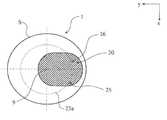
층 배열체 자체에 대한 동일한 연속체의 동일한 재료들은 중간 층 또는 중간 층 배열체를 위한 재료로 사용될 수 있다. 그러나, 중간 층 배열체의 경우에, 중간 층 또는 중간 층 배열체가 미러의 반사율에 일반적으로 무시할 만한 정도의 기여를 하고 따라서 배리어 층에 의한 대조의 증가의 문제는 이 경우에 중요하지 않으므로, 개별 층들 사이에 배리어 층이 없을 수도 있다. 교번하는 크로뮴과 스칸듐 층들 또는 비정질 몰리브덴과 루테늄 층들로 이루어진 다층 배열체들은 유사하게 중간 층 또는 중간 층 배열체로서 생각될 수 있을 것이다. 후자는 예를 들어 20nm보다 큰 두께의 관점에서 선택될 수 있어, 밑에 놓인 기판이 충분히 EUV 방사로부터 보호된다. 이 경우, 이러한 층들은 소위 "표면 보호 층(SPL)"으로서 기능하며 보호층으로서 EUV 방사로부터의 보호를 제공할 것이다.The same materials of the same continuum to the layer arrangement itself can be used as the material for the intermediate layer or intermediate layer arrangement. However, in the case of an intermediate layer arrangement, since the intermediate or intermediate layer arrangement generally makes a negligible contribution to the reflectivity of the mirror and thus the problem of increased contrast by the barrier layer is not important in this case, There may be no barrier layer. Multilayer arrays of alternating chromium and scandium layers or amorphous molybdenum and ruthenium layers may similarly be thought of as intermediate or intermediate layer arrangements. The latter can be selected, for example, in terms of thicknesses greater than 20 nm, so that the underlying substrate is sufficiently protected from EUV radiation. In this case, these layers will function as so-called "surface protective layer (SPL) " and will provide protection from EUV radiation as a protective layer.
본 발명에 따른 미러들(1a, 1b, 1c)의 층 배열체들은 종단 층(terminating layer)(M)으로서, 예를 들어, Rh, Pt, Ru, Pd, Au, SiO2 등과 같은 화학적으로 불활성인 재료로 이루어지는 적어도 하나의 층을 포함하는 덮개 층 시스템(C)에 의해 도 1 내지 도 3에서 종단된다. 이러한 종단 층(M)은 따라서 주위의 영향들로 인한 미러 표면의 화학적 변화를 방지한다. 도 1 내지 도 3의 덮개 층 시스템(C)은, 이러한 종단 층(M) 외에, 고 굴절률 층(H), 저 굴절률 층(L) 및 배리어 층(B)으로 구성된다.The layer arrangements of the
주기들(P1, P2, P3) 중의 하나의 두께는 도 1 내지 도 3으로부터 해당 주기의 개별 층들의 두께들의 합으로서, 즉, 고 굴절률 층의 두께, 저 굴절률 층의 두께 및 2개의 배리어 층들의 두께의 합이다. 결과적으로, 도 1 내지 도 3에서의 층 서브시스템들(P', P'', P''')은 그 주기들(P1, P2, P3)이 서로 다른 두께(d1, d2, d3)를 갖는다는 사실로 인해 서로 구분될 수 있다. 그 결과, 본 발명의 내용에 있어서, 다른 층 서브시스템들(P', P'', P''')은 그 주기들(P1, P2, P3)이 두께(d1, d2, d3)에 있어서 0.1 nm를 초과하는 만큼 다른 층 서브시스템들인 것으로 이해되는데, 이는 고 굴절률 층과 저 굴절률 층 사이의 주기들의 동일한 분할이 다르게 주어지는 경우, 0.1nm의 차이 미만에서는 층 서브시스템들의 다른 광학적 효과가 더 이상 취해질 수 없기 때문이다. 또한, 본래 동일한 층 서브시스템들은 다른 생산 장치들 상에서의 생산 동안에 그 주기 두께들에 있어서 절대적인 수치에 의해 요동할 수 있다. 몰리브덴과 실리콘으로 구성된 주기를 갖는 층 서브시스템(P', P'', P''')의 경우에 대해, 이미 상술한 바와 같이, 이 경우 주기(P1, P2, P3) 내에 제2 배리어 층이 없는 것이 가능하여, 주기들(P1, P2, P3)의 두께가 고 굴절률 층의 두께, 저 굴절률 층의 두께 및 배리어 층들의 두께로부터 도출된다.The thickness of one of the periods (P1 , P2 , P3 ) is determined from FIGS. 1 to 3 as the sum of the thicknesses of the individual layers of the period, that is, the thickness of the high refractive index layer, the thickness of the low refractive index layer, Thickness of the barrier layers. As a result, the layer subsystems P ', P'',P''' in FIGS. 1 to 3 are arranged such that their periods P1 , P2 and P3 have different thicknesses d1 and
도 4는 도 8 내지 도 15에 대한 예시적 실시예들에 따른 본 발명의 미러들(1a, 1b, 1c)에 기초하여 구성된 적어도 하나의 미러(1)를 구비하는, 6개의 미러들(1, 11)을 갖는 마이크로리소그래피용 투영 노광 장치를 위한 본 발명에 따른 투영 대물부(2)의 개략적인 도면을 도시한다. 마이크로리소그래피용 투영 노광 장치의 기능은 레티클(reticle)로도 지칭되는 마스크의 구조들을 소위 결상 평면의 웨이퍼 상에 리소그래픽 기법에 의해 결상하는 것이다. 이러한 목적으로, 도 4의 본 발명에 따른 투영 대물부(2)는 대상물 평면(5)에 배열된 대상물 필드(object field)(3)를 결상 평면(7)의 결상 필드(image field) 내로 결상한다. 명료함을 위해서 도면에 도시되지 않은 구조를 지지하는 마스크는 대상물 평면(5)의 대상물 필드(3)의 위치에 배열될 수 있다. 배향을 위해, 도 4는 그 x-축이 도면의 평면을 향하는 테카르트 좌표 시스템을 도시한다. 이 경우, x-y 좌표 평면은 대상물 평면(5)과 일치하고, z-축은 대상물 평면(5)에 수직하면서 아래 방향을 가리킨다. 이러한 투영 대물부는 대상물 필드(3)을 통과하지 않는 광축(9)을 갖는다. 투영 대물부(2)의 미러들(1, 11)은 광축에 대해서 회전 방향으로 대칭인 설계 표면을 갖는다. 이 경우, 이러한 설계 표면은 완성된 미러의 물리적 표면과 혼동되어서는 아니되며, 이유는 물리적 표면이 미러를 지나는 빛의 통로를 확보하기 위해서 설계 표면에 대해 상대적으로 트리밍되어야 하기 때문이다. 본 예시적 실시예에서, 구경 조리개(13)가 대상물 평면(5)으로부터 결상 평면(7)으로의 광 경로에서 제2 미러(11) 상에 배열된다. 투영 대물부(2)의 효과가 3개의 광선, 즉 주 광선(15)과 2개의 구경 주변광(17, 19)의 도움을 받아 도시되었으며, 이 모두는 대상물 필드(3)의 중심에서 나온다. 대상물 평면의 수직에 대해 6°의 각으로 진행하는 주 광선(15)은 구경 조리개(13)의 평면에서 광축(9)과 교차한다. 대상물 평면(5)으로부터 보았을 때, 주 광선(15)은 입구 동공 평면(entrance pupil plane)(21) 내에서 광축과 교차하는 것으로 보인다. 이는 제1 미러(11)를 통한 주 광선(15)의 점선(dash)으로 표시된 연장선에 의해 도 4에서 지시된다. 그 결과, 구경 조리개(13)의 가상 화상, 입구 동공은 입구 동공 평면(21)에 놓인다. 투영 대물부의 출구 동공은 유사하게 결상 평면(7)으로부터 진행하는 주 광선(15)의 후방 연장선에서 동일한 구성과 함께 찾을 수 있었다. 그러나, 결상 평면(7)에서, 주 광선(15)은 광축(9)에 평행하며, 이로부터, 이러한 2개의 광선들의 후방 투영이 투영 대물부(2)의 전방의 무한대에 교차 지점을 생성할 수 있으며, 따라서 투영 대물부(2)의 출구 동공은 따라서 무한대에 있다. 따라서, 이 투영 대물부(2)는 결상 측에서 소위 단부 동원체(telecentric)인 대물부이다. 대상물 필드로부터 방출되는 방사의 바람직하지 않은 비그네팅(vignetting)이 투영 대물부의 반사 구성의 경우에 발생하지 않도록, 대상물 필드(3)의 중심은 광축(9)으로부터 거리 R이고, 결상 필드(7)의 중심은 광축(9)으로부터 거리 r이다.Figure 4 shows a perspective view of six mirrors 1 (1), 1 (2), 1 < RTI ID = 0.0 > , 11) for a projection exposure apparatus for microlithography according to the present invention. The function of the projection exposure apparatus for microlithography is to image the structures of the mask, also referred to as a reticle, by a lithographic technique on a wafer of so-called imaging plane. For this purpose, the
도 5는 도 4에 도시된 투영 대물부(2)에 발생하는 것과 같은 아치형 결상 필드(7a)와, 도 4의 것에 해당하는 축들을 갖는 테카르트 좌표계의 평면도를 도시한다. 결상 필드(7a)는 그 중심이 대상물 평면과 광축(9)의 교차 지점에 의해 주어지는 환형의 일부이다. 도시된 경우에 있어서, 평균 반경(r)은 34mm이다. 여기서, y-방향으로의 필드의 폭(d)은 2mm이다. 결상 필드(7a)의 중심 필드 지점은 결상 필드(7a) 내에서 작은 원으로 표시되어 있다. 다른 방법으로서, 만곡된 결상 필드는 동일한 반경을 가지며 y-방향으로 서로 변위된 2개의 원호들에 의해 또한 경계가 형성될 수 있다. 만약 투영 노광 장치가 스캐너로서 동작하면, 스캐닝 방향은 대상물 필드의 더 짧은 범위의 방향으로, 즉 y-방향으로 뻗을 수 있다.Fig. 5 shows a top view of a tertiary coordinate system having
도 6은 도 4에서 투영 대물부(2)의 대상물 평면(5)으로부터 결상 평면(7)까지의 광 경로에서의 끝에서 두번 째인 미러(1)의 광축과 미러 표면 사이의 다른 반경 또는 거리[단위(mm)]에 대한 입사각 간격들(원들)의 간격 길이 및 최대 입사각들(사각형들)[단위 (°)]을 예시적으로 도시한다. EUV 파장 범위용의 6개의 미러들(1, 11)을 갖는 마이크로리소그래피용 투영 대물부(2)의 경우에, 이러한 미러(1)는 일반적으로 가장 큰 입사각들과 가장 큰 입사각 간격들 또는 입사각들의 가장 큰 변경을 확보해야만 하는 미러이다. 본 원의 내용에 있어서, 입사각들의 변경의 정도로서의 입사각 간격의 길이는 광학적 설계의 요건으로 인해 광축으로부터의 주어진 거리에 대해 미러의 코팅이 확보해야하는 최대 및 최소 입사각들 사이의 각도 정도들의 각 범위의 각 정도들의 개수이다. 입사각 간격은 또한 AOI 간격으로 간략히 표현될 수 있다.Fig. 6 is a diagram showing another radius or distance between the optical axis of the mirror 1, which is the second time from the end in the optical path from the
표 1에 따른 투영 대물부의 광학 데이터는 도 6이 기초로 하고 있는 미러(1)의 경우에 적용 가능하다. 이 경우, 광학 설계의 미러들(1, 11)의 비구형들(aspheres)은 하기의 비구형 방정식에 따른 비구형 정점에서의 법선(normal)에 대한 비구형 지점의 수직한 거리(h)의 함수로서 비구형 정점에서의 접평면(tangential plane)에 대한 비구형 지점의 수직 거리(Z(h))에 의해 회전 방향으로 대칭인 평면들로서 규정된다:The optical data of the projection objective according to Table 1 is applicable to the case of the mirror 1 based on Fig. In this case, the aspheres of the
Z(h)=(rho*h2)/(1+[1-(1+ky)*(rho*h)2]0.5)+c1*h4+c2*h6+c3*h8+c4*h10+c5*h12+c6*h14Z (h) = (rho * h 2) / (1+ [1- (1 + k y) * (rho * h) 2] 0.5) + c 1 * h 4 +
이때, 반경(R)은 미러의 1/rho이고, 변수들 ky, c1, c2, c3, c4, c5, c6의 단위는 mm이다. 이 경우, 위 변수들 cn은 또한 단위[mm]인 거리(h)의 함수로서 비구형(Z(h))의 결과를 가져오는 방식으로 [1/mm2n+2]에 따른 단위[mm]에 대해 정규화된다.In this case, the radius R is 1 / rho of the mirror, and the units of the variables ky , c1 , c2 , c3 , c4 , c5 and c6 are mm. In this case, the above variables cn are also expressed in units [mm / mm2 ] according to [1 / mm2n+ 2 ] in such a way as to result in the unsymmetrical (Z ≪ / RTI >


표 1: 도 4에 기초하는 설계의 개략적인 도시에 따른 도 6에서의 미러(1)의 입사각들에 관한 광학적 설계의 데이터Table 1: Data of the optical design relating to the angles of incidence of the mirror 1 in Fig. 6 according to the schematic illustration of the design based on Fig.
도 6으로부터 24°의 최대 입사각들과 11°의 간격 길이들이 미러(1)의 서로 다른 위치들에서 발생함을 알 수 있다. 결과적으로, 미러(1)의 층 배열체는 다른 입사각들과 다른 입사각 간격들의 이러한 다른 위치들에서 높고 균일한 반사율 수치를 산출해야 하는데, 이는 그렇지 않으면 투영 대물부(2)의 높은 총 투과율과 허용되는 동공 애퍼디제이션이 확보될 수 없기 때문이다.It can be seen from FIG. 6 that the maximum incidence angles of 24 DEG and the interval lengths of 11 DEG occur at different positions of the mirror 1. As a result, the layer arrangement of the mirror 1 must produce a high and uniform reflectance value at these different positions of the incidence angles different from the other incidence angles, which would otherwise lead to a high total transmittance of the
소위 PV 수치는 입사각들에 대한 미러의 반사율의 변경의 척도로서 사용될 수 있다. 이 경우, PV 수치는 고려되는 입사각 간격에서의 평균 반사율(Raverage)에 의해 분할된 고려되는 입사각 간격에서의 최소 반사율(Rmin)과 최대 반사율(Rmax) 사이의 차이로서 정의된다. 결과적으로, PV=(Rmax-Rmin)/Raverage가 참인 상태로 유지된다.The so-called PV value can be used as a measure of the change in reflectivity of the mirror to incident angles. In this case, the PV value is defined as the difference between the minimum reflectance (Rmin ) and the maximum reflectivity (Rmax ) at the considered angle of incidence divided by the average reflectance (Raverage ) at the angle of incidence considered. As a result, PV = (Rmax -Rmin ) / Raverage remains true.
이 경우, 도 4와 표 1의 설계에 따른 결상 평면(7) 앞의 끝에서 두번 째의 미러인 투영 대물부(2)의 미러(1)에 대한 높은 PV 수치들이 동공 애퍼디제이션에 대한 높은 수치들을 가져 온다는 점이 고려되어야 한다. 이 경우, 미러(1)의 PV 수치와 0.25보다 큰 높은 PV 수치들에 대한 투영 대물부(2)의 동공 애퍼디제이션의 결상 수차 사이에는 상관 관계가 있는데, 이는 이 수치로부터 PV 수치가 수차의 다른 원인들에 대한 동공 애퍼디제이션을 지배하기 때문이다.In this case, the high PV values for the mirror 1 of the
도 6에서, 예를 들어, 약 21°의 관련 최대 입사각과 광축에 대한 11°의 관련 간격 길이를 갖는 미러(1)의 위치들의 특정 반경 또는 특정 거리를 표시하기 위해 바(23)가 사용된다. 이러한 표시된 반경은 후술하는 바와 같이, 도 7에서, 미러(1)의 광학적으로 활용되는 영역(20)을 나타내는 빗금 영역(20) 내에서, 점선으로 표시된 원(23a)의 위치들에 대응한다.In FIG. 6, for example, a
도 7은 평면도에서 광축(9)에 대해 중심에 위치하는 원으로서 도 4로부터의 대상물 평면(5)에서 투영 대물부(2)의 결상 평면(7)으로의 광 경로에 있는 끝에서 두번 째의 미러(1)의 기판(S)을 보여준다. 이 경우, 투영 대물부(2)의 광축(9)은 기판의 대칭 축(9)에 대응한다. 더욱이, 도 7에서, 광축에 대해 옵셋된 미러(1)의 광학적으로 활용되는 영역(20)은 빗금 방식으로 도시되어 있으며, 원(23a)은 점선 방식으로 도시되어 있다.Fig. 7 is a schematic view of the second object from the end in the light path from the
이 경우, 광학적으로 활용되는 영역의 점선으로 표시된 원(23a)의 일부는 도 6에 도시된 바(23)에 의해 표시된 미러(1)의 위치들에 대응한다. 그 결과, 도 6으로부터의 데이터에 따라, 광학적으로 활용된 영역(20) 내의 점선으로 표시된 원(23a)의 부분적 영역을 따라서 있는 미러(1)의 층 배열체는 21°의 최대 입사각과 약 10°의 최소 입사각 양자에 대해 고 굴절률 수치들을 보장해야 한다. 이 경우, 약 10°의 최소 입사각은 11°의 간격 길이로 인해서 도 6으로부터 21°의 최대 입사각으로부터 기인한다. 상술한 2개의 극한 입사각 수치들이 발생하는 점선으로 표시된 원의 위치들은 10°의 입사각에 대한 화살표(26)의 끝단에 의해 그리고 21°의 입사각에 대한 화살표(25)의 끝단에 의해 도 7에서 강조된다.In this case, a part of the
층 배열체는 높은 기술적 경비가 들지 않고 기판(S)의 위치들에 대해 국부적으로 변경될 수 없으며 층 배열체들은 일반적으로 기판의 대칭 축(9)에 대해 회전 방향으로 대칭으로 적용되므로, 도 7에서 점선으로 표시된 원(23a)의 위치들을 다르는 층 배열체는 도 1 내지 도 3의 기본 구조에 도시된 것과 같이 하나의 그리고 동일한 층을 포함하고, 도 8 내지 도 15를 참조하여 특정 예시적 실시예들의 형태로 설명된다. 이 경우, 층 배열체를 갖는 기판(S)의 대칭 축(9)에 대한 기판(S)의 회전 방향으로 대칭인 코팅이 층 배열체의 층 서브시스템들(P', P'', P''')의 주기적 연속체가 미러의 모든 위치들에서 유지되고 대칭 축(9)으로부터의 거리에 따라 달라지는 층 배열체의 주기들의 두께만이 기판(S)에 대한 회전 방향으로 대칭인 프로파일을 얻으며, 층 배열체는 대칭 축(9)에서 기판(S)의 중심에서보다 기판(S)의 에지에서 더 얇은 효과를 갖는다는 점이 고려되어야 한다.The layer arrangement can not be locally altered with respect to the positions of the substrate S without high technical expense and the layer arrangements are generally applied symmetrically in the rotational direction with respect to the
적절한 코팅 기술에 의해, 예를 들어, 분배 다이어프램들을 사용함으로써, 기판에 대한 코팅의 두께의 회전 방향으로 대칭인 반경 방향 프로파일에 적절하도록 하는 것이 가능한 점이 고려되어야 한다. 그 결과, 코팅 설계 자체에 부가하여, 기판에 대한 코팅 설계의 소위 두께 인자의 반경 방향 프로파일을 가지고서, 추가적인 자유도가 코팅 설계를 최적화하기 위해 가능하다.It should be considered that by suitable coating techniques, for example, by using dispensing diaphragms, it is possible to make them suitable for a radial profile that is symmetrical in the direction of rotation of the thickness of the coating to the substrate. As a result, in addition to the coating design itself, additional degrees of freedom are possible to optimize the coating design, with a radial profile of the so-called thickness factor of the coating design on the substrate.
도 8 내지 도 15에 도시된 반사율 수치들은 13.5nm의 파장에서 활용 가능한 재료들에 대한 표 2에 표시된 복합적 굴절률들(
표 2: 13.5nm에 대해 채용된 굴절률들(
더욱이, 도 1 내지 도 3에 대한 층 연속체에 따른 하기의 짧은 표시(notation)이 도 8 내지 도 15와 연관된 층 설계들에 대해서 선언된다.Furthermore, the following short notation in accordance with the layer continuum for Figs. 1-3 is declared for the layer designs associated with Figs. 8-15.
기판 / ... / (P1)*N1 / (P2)*N2 / (P3)*N3 / 덮개 층 시스템 CSubstrate / ... / (P1 ) * N1 / (P2 ) * N2 / (P3 ) * N3 /
여기서, 도 2와 도 3에 대해서, P1=H'BL'B; P2=H''BL''B; P3=H'''BL'''B; C=HBLM이고, 도 1과 도 3에 대한 변형례인 제4 예시적 실시예에 대해서, P1=BH'BL';P2=BL''BH''; P3=H'''BL'''B; C=HBLM이다.2 and 3, P1 = H'BL'B; P2 = H " BL "B; P3 = H '''BL'''B; For a fourth exemplary embodiment, where C = HBLM and a variation on FIGS. 1 and 3, P1 = BH'BL ';P2=BL''BH '' ; P3 = H '''BL'''B; C = HBLM.
이 경우, 문자 H는 고 굴절률 층들의 두께를 기호적으로 나타내고, 문자 L은 저 굴절률 층들의 두께를 나타내고, 문자 B는 배리어 층의 두께를 나타내고, 문자 M은 도 2와 도 1 내지 도 3에 관한 기재에 따라 화학적으로 불활성인 종단층의 두께를 나타낸다.In this case, the letter H represents the thickness of the high refractive index layers symbolically, the letter L represents the thickness of the low refractive index layers, the letter B represents the thickness of the barrier layer, Lt; RTI ID = 0.0 > chemically < / RTI >
이 경우, 단위 [nm]는 괄호 사이에서 규정된 개별 층들의 두께에 적용된다. 도 8과 도 9에 대해 사용되는 층 설계는 따라서 다음과 같이 짧은 표시로서 규정될 수 있다.In this case, the unit [nm] is applied to the thickness of the individual layers defined between the parentheses. The layer design used for Figs. 8 and 9 can thus be defined as a short designation as follows.
기판/.../ (0.4B4C2.921Si0.4B4C4.931Mo)*8/ (0.4B4C4.145Mo0.4B4C2.911Si)*5 / (3.509Si0.4B4C3.216Mo0.4B4C)*16 / 2.975Si0.4B4C2Mo1.5RuSubstrate / (0.4B4C 2.921Si 0.4B4C 4.931Mo ) *8 / (0.4B4C 4.145Mo 0.4B4C 2.911Si ) * 5 / (3.509Si 0.4B4C 3.216Mo 0.4B4C ) * 16 / 2.975Si 0.4B4C 2Mo 1.5Ru
본 예에서 배리어 층(B4C)은 항상 두께가 0.4nm이므로, 도 8과 도 9에 대한 층 설계가 다음과 같이 짧은 방식으로 특정될 수 있도록, 층 배열체의 기본 구조를 도시하기 위해 또한 생략될 수 있다.In this example, the barrier layer (B4 C) is always 0.4 nm thick, so that the layer design for Figures 8 and 9 can be specified in a short way as follows: Can be omitted.
기판/.../ (2.921Si4.931Mo)*8 / (4.415Mo2.911Si)*5 / (3.509Si3.216Mo)*16 / 2.975Si2Mo1.5RuSubstrate / (2.921Si 4.931Mo ) * 8 / (4.415Mo 2.911Si ) * 5 / (3.509Si 3.216Mo ) * 16 / 2.975
도 1에 따른 제1 예시적 실시예로부터, 3.509nm의 두께를 가지고 기판으로부터 가장 멀리 있는 층 서브시스템의 제1 고 굴절률 층이 2.911nm의 두께를 가지고 기판으로부터 둘째로 가장 멀리 있는 층 서브시스템의 마지막 고 굴절률 층과 직접 연속되도록, 5개의 주기들을 포함하는 제2 층 서브시스템에서의 고 굴절률 층(Si)와 저 굴절률 층(Mo)의 순서가 다른 층 서브시스템들에 대해 역순이었다는 점이 인식되어야 한다.From the first exemplary embodiment according to Figure 1, the first high refractive index layer of the layer subsystem furthest from the substrate with a thickness of 3.509 nm has a thickness of 2.911 nm and the secondmost furthest from the substrate It should be appreciated that the order of the high refractive index layer (Si) and the low refractive index layer (Mo) in the second layer subsystem including five periods is in reverse order with respect to the other layer subsystems so as to be directly continuous with the last high refractive index layer do.
따라서, 다음과 같은 짧은 표시로서, 도 2에 따른 제2 예시적 실시예로서 도 10과 도 11에 대해 사용되는 층 설계를 특정하는 것이 가능하다.Therefore, it is possible to specify the layer design used for Figs. 10 and 11 as a second exemplary embodiment according to Fig. 2, with the following short indications.
기판/.../ (4.737Si0.4B4C2.342Mo0.4B4C)*28 / (3.443Si0.4B4C2.153Mo0.4B4C)*5 / (3.523Si0.4B4C3.193Mo0.4B4C)*15 / 2.918Si0.4B4C2Mo1.5RuSubstrate / (4.737Si 0.4B4C 2.342Mo 0.4B4C ) * 28 / (3.443Si 0.4B4C 2.153Mo 0.4B4C ) * 5 / (3.523Si 0.4B4C 3.193Mo 0.4B4C ) * 15 / 2.918Si 0.4B4C 2Mo 1.5Ru
예에서 배리어 층(B4C)은 항상 두께가 0.4nm이므로, 도 10과 도 11에 대한 층 설계가 다음과 같이 짧은 방식으로 특정될 수 있도록, 층 배열체를 도시하기 위해 또한 생략될 수 있다.In the example, since the barrier layer (B4 C) is always 0.4 nm thick, it can also be omitted to show the layer arrangement, so that the layer design for Figures 10 and 11 can be specified in the following short way .
기판/.../ (4.737Si2.342Mo)*28 / (3.443Si2.153Mo)*5 / (3.523Si3.193Mo)*15 / 2.918Si2Mo1.5RuSubstrate / (4.737Si 2.342Mo ) * 28 / (3.443Si 2.153Mo ) * 5 / (3.523Si 3.193Mo ) * 15 / 2.918
따라서, 다음과 같은 짧은 표시로서, 도 3에 따른 제3 예시적 실시예로서 도 12과 도 13에 대해 사용되는 층 설계를 특정하는 것이 가능하다.Thus, it is possible to specify the layer design used for Figs. 12 and 13 as a third exemplary embodiment according to Fig. 3, with the following short indications.
기판/.../ (1.678Si0.4B4C5.665Mo0.4B4C)*27 / (3.798Si0.4B4C2.855Mo0.4B4C)*14 / 1.499Si0.4B4C2Mo1.5RuSubstrate / ... / (1.678Si0.4B4C5.665Mo0.4B4C) * 27 / (3.798Si0.4B4C2.855Mo0.4B4C) * 14 / 1.499Si0.4B4C2Mo1.5Ru
도시를 목적으로 배리어 층 B4C를 무시하면 다음과 같다.For purposes of illustration, the barrier layer B4 C is ignored as follows.
기판/.../ (1.678Si5.665Mo)*27 / (3.798Si2.855Mo)*14 / 1.499Si2Mo1.5RuSubstrate / ... (1.678Si 5.665Mo ) * 27 / (3.798Si 2.855Mo ) * 14 / 1.499
유사하게, 다음과 같은 짧은 표시로서, 도 3에 대한 변형에 따른 제4 예시적 실시예로서 도 14과 도 15에 대해 사용되는 층 설계를 특정하는 것이 가능하다.Similarly, it is possible to specify the layer design used for Figs. 14 and 15 as a fourth exemplary embodiment according to the variant to Fig. 3, with the following short indications.
기판/.../ (0.4B4C4.132Mo0.4B4C2.78Si)*6 / (3.608Si0.4B4C3.142Mo0.4B4C)*16 / 2.027Si0.4B4C2Mo1.5RuSubstrate / ... (0.4B4C4.132Mo0.4B4C2.78Si) * 6 / (3.608Si0.4B4C3.142Mo0.4B4C) * 16 / 2.027Si0.4B4C2Mo1.5Ru
도시를 목적으로 배리어 층 B4C를 무시하면 다음과 같다.For purposes of illustration, the barrier layer B4 C is ignored as follows.
기판 /.../ (4.132Mo02.78Si)*6 / (3.608Si3.142Mo)*16 / 2.027Si2Mo1.5RuSubstrate / ... (4.132Mo 02.78Si ) * 6 / (3.608Si 3.142Mo ) * 16 / 2.027
제4 예시적 실시예로부터, 3.609nm의 두께를 가지고 기판으로부터 가장 멀리 있는 층 서브시스템(P''')의 제1 고 굴절률 층이, 2.78nm의 두께를 가지고 기판으로부터 둘째로 가장 멀리 있는 층 서브시스템(P'')의 마지막 고 굴절률 층과 직접 연속되도록, 6개의 주기들을 포함하는 층 서브시스템(P'')에서의 고 굴절률 층(Si)과 저 굴절률 층(Mo)의 순서가 16개의 주기를 갖는 다른 층 서브시스템들과 상대적으로 역이 되었다는 점이 인식되어야 한다.From the fourth exemplary embodiment, the first high refractive index layer of the layer subsystem P " ', which is the furthest from the substrate with a thickness of 3.609 nm, has a thickness of 2.78 nm and is the second furthest from the substrate The order of the high refractive index layer Si and the low refractive index layer Mo in the layer sub-system P " including six periods is directly set to 16 Lt; RTI ID = 0.0 > 1 < / RTI > periods.
따라서, 제4 예시적 실시예는 기판으로부터 둘째로 멀리 있는 층 서브시스템(P'')에서의 고 및 저 굴절률들의 순서가 도 1에 대한 제1 예시적 실시예에 따라 역순인 제3 예시적 실시예의 변형이다.Thus, the fourth exemplary embodiment is similar to the first exemplary embodiment of FIG. 1 except that the order of the high and low refractive indexes in the layer sub-system P " Fig.
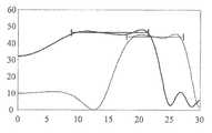
도 8은 단위 [°]로 입사각에 대해 표시된 도 1에 따른 본 발명을 따르는 미러(1a)의 제1 예시적 실시예의 단위 [%]로의 비극성 방사에 대한 반사율 수치들을 보여준다. 이 경우, 미러(1a)의 층 배열체의 제1 층 서브시스템(P')은 N1=8개의 주기들(P1)로 이루어지고, 주기(P1)는 고 굴절률 층으로서 2.921nm Si와 저 굴절률 층으로서 4.931nm Mo와, 각각 0.4nm B4C를 포함하는 2개의 배리어 층들로 구성된다. 주기(P1)는 결과적으로 8.652nm의 두께(d1)를 갖는다. 층들(Mo, Si)의 역순을 갖는 미러(1a)의 층 배열체의 제2 층 서브시스템(P'')은 N2=5개의 주기들(P2)로 구성되며, 주기(P2)는 고 굴절률 층으로서 2.911nm Si와 저 굴절률 층으로서 4.145nm Mo와, 각각 0.4nm B4C를 포함하는 2개의 배리어 층들로 구성된다. 주기(P2)는 결과적으로 7.856nm의 두께(d2)를 갖는다. 미러(1a)의 층 배열체의 제3 층 서브시스템(P''')은 N3=16개의 주기들(P3)로 이루어지고, 주기(P3)는 고 굴절률 층으로서 3.509nm Si와 저 굴절률 층으로서 3.216nm Mo와, 각각 0.4nm B4C를 포함하는 2개의 배리어 층들로 구성된다. 주기(P3)는 결과적으로 7.525nm의 두께(d3)를 갖는다. 미러(1a)의 층 배열체는 특정된 순서대로 2.975nm Si, 0.4nm B4C, 2nm Mo 및 1.5nm Ru로 이루어진 덮개 층 시스템(C)에 의해 종단된다. 그 결과, 기판으로부터 가장 멀리 있는 층 서브시스템(P''')은 기판으로부터 둘째로 가장 멀리 있는 층 서브시스템(P'')에 대한 주기들(P2)의 개수(N2)보다 큰 주기들(P3)의 개수(N3)를 가지며, 기판으로부터 가장 멀리 있는 층 서브시스템(P''')의 첫째 고 굴절률 층(H''')은 기판으로부터 둘째로 멀리 있는 층 서브시스템(P'')의 마지막 고 굴절률 층(H'')과 직접적으로 연속된다.Figure 8 shows the reflectance values for the non-polarized radiation in units [%] of the first exemplary embodiment of the mirror 1a according to the invention according to Figure 1, expressed in terms of incidence angle in units [deg.]. In this case, the first layer subsystem P 'of the layer arrangement of the mirror 1a consists of N1 = 8 periods P1 and the period P1 is 2.921 nm Si 4.931 nm Mo as a low refractive index layer, and two barrier layers each containing 0.4 nm B4 C. The period (P1 ) consequently has a thickness (d1 ) of 8.652 nm. Layers of a second layer subsystem (P '') of the layer arrangement of the mirror (1a) having the reverse of the (Mo, Si) is composed of N2 = 5 of periods (P2), period (P2) Is composed of two barrier layers including 2.911 nm Si as a high refractive index layer, 4.145 nm Mo as a low refractive index layer, and 0.4 nm B4 C, respectively. The period (P2 ) consequently has a thickness (d2 ) of 7.856 nm. The third layer subsystem P '''of the layer arrangement of the mirror 1a consists of N3 = 16 periods P3 and the period P3 is composed of 3.509 nm Si and 3.216 nm of Mo as a low refractive index layer, and two barrier layers of 0.4 nm B4 C each. The period (P3 ) consequently has a thickness (d3 ) of 7.525 nm. The layer arrangement of the mirror 1a is terminated by a cover layer system (C) consisting of 2.975 nm Si, 0.4 nm B4 C, 2 nm Mo and 1.5 nm Ru in the specified order. As a result, the layer farthest from the substrate subsystem (P ''') is a second layer subsystem (P farthest in from the substrate, large period than the number (N2) of the periods (P2) for') the (P3), the number (N3) to have the layer farthest from the substrate subsystem (P '''), the first high refractive index layer (H a''') is a layer subsystem in as far as the second from the substrate of ( Is directly continuous with the last high refractive index layer H "
13.5nm의 파장에서 단위 [%]의 두께 인자 1을 갖는 이 명목상의 층 설계의 반사율 수치들이 도 8에 단위 [°]의 입사각에 대한 실선으로 도시되어 있다. 더욱이, 14.1°내지 25.7°의 입사각 간격에 대한 이 명목상 층 설계의 평균 반사율은 수평 실선 바로서 묘사되어 있다. 또한, 도 8은 따라서 13.5nm의 파장에서 또한 0.933의 두께 인자가 주어지면, 점선으로서, 입사각들에 대한 반사각 수치들과, 점선 바로서, 2.5°내지 7.3°의 입사각 간격에 대한 상기 특정된 층 설계의 평균 반사율을 특정한다. 그 결과, 도 8에 점선으로 도시된 반사율 수치들에 대한 층 배열체의 주기들의 두께는 위 명목상 층 설계의 주기들의 해당 두께들의 단지 93.3%에 달한다. 환언하면, 이 층 배열체는 2.5°와 7.3° 사이의 입사각들이 확보되어야 하는 위치들에서 미러(1a)의 미러 표면에서 6.7% 만큼 명목상 층 설계보다 얇다.Reflectance values of this nominal layer design with thickness factor 1 in units [%] at a wavelength of 13.5 nm are shown in solid lines for the angle of incidence of the unit [°] in FIG. Moreover, the average reflectance of this nominal layer design for an incident angle interval of 14.1 DEG to 25.7 DEG is depicted as a horizontal solid line bar. Figure 8 also shows that, given the thickness factor of 0.933 and also at a wavelength of 13.5 nm, the dotted line shows the reflection angle values for the incident angles and the specified layer for the angle of incidence of 2.5 to 7.3, Identify the average reflectance of the design. As a result, the thicknesses of the periods of the layer arrangement for the reflectance values shown in dashed lines in Fig. 8 reach only 93.3% of the corresponding thicknesses of the periods of the nominal layer design above. In other words, this layer arrangement is thinner than the nominal layer design by 6.7% at the mirror surface of the mirror 1a at locations where the angles of incidence between 2.5 and 7.3 should be ensured.
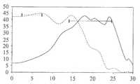
도 9는 13.5nm의 파장과 1.018의 두께 인자가 주어지면, 도 8에 대응하는 방식으로, 얇은 선으로서, 입사각들에 대한 반사율 수치들을, 얇은 바로서, 17.8°내지 27.2°의 입사각 간격에 대한 상기 특정된 층의 평균 반사율을 보여주면, 또한, 0.972의 두께 인자가 주어지면, 대응하는 방식으로, 두꺼운 선으로서, 입사각들에 대한 반사율 수치들을, 두꺼운 바로서, 8.7° 내지 21.4°의 입사각 간격들에 대한 상기 특정된 층 설계의 평균 반사율을 보여준다. 그 결과, 이 층 배열체는 17.8°와 27.2°사이의 입사각들이 확보되어야 하는 위치에서 미러(1a)의 미러 표면에서 1.8% 만큼 명목상 층 설계보다 두꺼우며, 따라서, 8.7°와 21.4° 사이의 입사각들이 확보되어야 하는 위치들에서, 2.8% 만큼 명목상 층 설계보다 얇다.9 shows the reflectance values for the incident angles, as a thin line, in a manner corresponding to Fig. 8, given a wavelength of 13.5 nm and a thickness factor of 1.018, for a thin barrel with an angle of incidence of 17.8 to 27.2 Given the average reflectivity of the specified layer, and given a thickness factor of 0.972, reflectance values for the angles of incidence, as thick lines, in corresponding manner, are measured in thick barrels at an angle of incidence of 8.7 to 21.4 ≪ / RTI > the average reflectivity of the specified layer design for the < RTI ID = 0.0 > As a result, this layer arrangement is thicker than the nominal layer design by 1.8% at the mirror surface of the mirror 1a at locations where the angles of incidence between 17.8 and 27.2 are to be ensured, and therefore the angle of incidence between 8.7 and 21.4 Are thinner than nominally layered designs by 2.8% at locations where they must be secured.
도 8과 도 9에 대한 층 배열체에 대해서 달성될 수 있는 평균 반사율과 PV 수치들은 표 3의 입사각 간격들과 두께 인자들에 대해 상대적으로 컴파일될 수 있다. 2.5°와 27.2°사이의 입사각들에 대해 13.5nm의 파장에서, 상기 특정된 층 배열체를 포함하는 본 발명에 따른 미러(1a)는 43%를 초과하는 평균 반사율과 0.21 이하의 PV 수치로서의 반사율의 변형을 갖는다.The average reflectivity and PV values that can be achieved for the layer arrangement for Figures 8 and 9 can be compiled relative to the incident angle intervals and thickness factors in Table 3. [ At a wavelength of 13.5 nm for angles of incidence between 2.5 and 27.2, the mirror 1a according to the invention comprising the specified layer arrangement has an average reflectance in excess of 43% and a reflectance in PV value of 0.21 or less .
표 3: 도(°)로 나타낸 입사각 간격과 선택된 두께 인자에 대한 도 8 및 도 9에 대한 층 설계의 평균 반사율 및 PV 수치들Table 3: Mean reflectivity and PV values of the layer design for Figs. 8 and 9 for incident angle spacing and selected thickness factor in degrees (degrees)
도 10은 단위 [°]로 입사각에 대해 표시된 도 2에 따라 본 발명에 따른 미러(1b)의 제2 예시적 실시예의 단위 [%]로의 비극성 방사에 대한 반사율 수치들을 보여준다. 이 경우, 미러(1b)의 층 배열체의 제1 층 서브시스템(P')은 N1=28개의 주기들(P1)로 이루어지고, 주기(P1)는 고 굴절률 층으로서 4.737nm Si와 저 굴절률 층으로서 2.342nm Mo와, 각각 0.4nm B4C를 포함하는 2개의 배리어 층들로 구성된다. 주기(P1)는 결과적으로 7.879nm의 두께(d1)를 갖는다. 미러(1b)의 층 배열체의 제2 층 서브시스템(P'')은 N2=5개의 주기들(P2)로 구성되며, 주기(P2)는 고 굴절률 층으로서 3.443nm Si와 저 굴절률 층으로서 2.153nm Mo와, 각각 0.4nm B4C를 포함하는 2개의 배리어 층들로 구성된다. 주기(P2)는 결과적으로 6.396nm의 두께(d2)를 갖는다. 미러(1b)의 층 배열체의 제3 층 서브시스템(P''')은 N3=15개의 주기들(P3)로 이루어지고, 주기(P3)는 고 굴절률 층으로서 3.523nm Si와 저 굴절률 층으로서 3.193nm Mo와, 각각 0.4nm B4C를 포함하는 2개의 배리어 층들로 구성된다. 주기(P3)는 결과적으로 7.516nm의 두께(d3)를 갖는다. 미러(1b)의 층 배열체는 특정된 순서대로 2.918nm Si, 0.4nm B4C, 2nm Mo 및 1.5nm Ru로 이루어진 덮개 층 시스템(C)에 의해 종단된다. 그 결과, 기판으로부터 가장 멀리 있는 층 서브시스템(P''')은 기판으로부터 둘째로 가장 멀리 있는 층 서브시스템(P'')에 대한 주기들(P2)의 개수(N2)보다 큰 주기들(P3)의 개수(N3)를 갖는다.Fig. 10 shows the reflectance values for the non-polar emission to the unit [%] of the second exemplary embodiment of the mirror 1b according to the present invention, according to Fig. 2, which is shown for the angle of incidence at the unit [deg.]. In this case, the first layer subsystem P 'of the layer arrangement of the mirror 1b consists of N1 = 28 periods P1 , and the period P1 is 4.737 nm Si 2.342 nm Mo as a low refractive index layer, and two barrier layers each containing 0.4 nm B4 C. The period (P1 ) results in a thickness (d1 ) of 7.879 nm. The second layer subsystem P '' of the layer arrangement of the mirror 1b consists of N2 = 5 periods P2 and the period P2 is a high refractive index layer of 3.443 nm Si and 2.153 nm of Mo as a refractive index layer, and two barrier layers of 0.4 nm B4 C each. The period (P2 ) consequently has a thickness (d2 ) of 6.396 nm. The third layer subsystem P '''of the layer arrangement of the mirror 1b consists of N3 = 15 periods P3 and the period P3 is composed of 3.523 nm Si as the high refractive index layer 3.193 nm Mo as a low refractive index layer, and two barrier layers each containing 0.4 nm B4 C. The period (P3 ) consequently has a thickness (d3 ) of 7.516 nm. The layer arrangement of mirror 1b is terminated by a cover layer system C consisting of 2.918 nm Si, 0.4 nm B4 C, 2 nm Mo and 1.5 nm Ru in the specified order. As a result, the layer farthest from the substrate subsystem (P ''') is a second layer subsystem (P farthest in from the substrate, large period than the number (N2) of the periods (P2) for') It has a number (N3) of the (P3).
13.5nm의 파장에서 단위 [%]의 두께 인자 1을 갖는 이 명목상의 층 설계의 반사율 수치들이 도 10에 단위 [°]의 입사각에 대한 실선으로 도시되어 있다. 더욱이, 14.1°내지 25.7°의 입사각 간격에 대한 이 명목상 층 설계의 평균 반사율은 수평 실선 바로서 묘사되어 있다. 또한, 도 10은 따라서 13.5nm의 파장에서 또한 0.933의 두께 인자가 주어지면, 점선으로서, 입사각들에 대한 반사각 수치들과, 점선 바로서, 2.5°내지 7.3°의 입사각 간격에 대한 상기 특정된 층 설계의 평균 반사율을 특정한다. 그 결과, 도 10에 점선으로 도시된 반사율 수치들에 대한 층 배열체의 주기들의 두께는 위 명목상 층 설계의 주기들의 해당 두께들의 단지 93.3%에 달한다. 환언하면, 이 층 배열체는 2.5°와 7.3° 사이의 입사각들이 확보되어야 하는 위치들에서 미러(1b)의 미러 표면에서 6.7% 만큼 명목상 층 설계보다 얇다.Reflectance values of this nominal layer design with thickness factor 1 in units [%] at a wavelength of 13.5 nm are plotted in FIG. 10 by solid lines for the angle of incidence in [°]. Moreover, the average reflectance of this nominal layer design for an incident angle interval of 14.1 DEG to 25.7 DEG is depicted as a horizontal solid line bar. Figure 10 also shows that, given the thickness factor of 0.933 and also at a wavelength of 13.5 nm, the dotted line shows the reflection angle values for the incident angles and the specified layer for the angle of incidence of 2.5 [deg.] To 7.3 [ Identify the average reflectance of the design. As a result, the thicknesses of the periods of the layer arrangement for the reflectance values shown in dashed lines in Fig. 10 reach only 93.3% of the corresponding thicknesses of the periods of the nominal layer design above. In other words, this layer arrangement is thinner than the nominal layer design by 6.7% at the mirror surface of mirror 1b at positions where the angles of incidence between 2.5 and 7.3 should be ensured.
도 11는 13.5nm의 파장과 1.018의 두께 인자가 주어지면, 도 10에 대응하는 방식으로, 얇은 선으로서, 입사각들에 대한 반사율 수치들을, 얇은 바로서, 17.8°내지 27.2°의 입사각 간격에 대한 상기 특정된 층의 평균 반사율을 보여주면, 또한, 0.972의 두께 인자가 주어지면, 대응하는 방식으로, 두꺼운 선으로서, 입사각들에 대한 반사율 수치들을, 두꺼운 바로서, 8.7° 내지 21.4°의 입사각 간격들에 대한 상기 특정된 층 설계의 평균 반사율을 보여준다. 그 결과, 이 층 배열체는 17.8°와 27.2°사이의 입사각들이 확보되어야 하는 위치에서 미러(1b)의 미러 표면에서 1.8% 만큼 명목상 층 설계보다 두꺼우며, 따라서, 8.7°와 21.4° 사이의 입사각들이 확보되어야 하는 위치들에서, 2.8% 만큼 명목상 층 설계보다 얇다.Figure 11 shows the reflectance values for the incident angles, as a thin line, in a manner corresponding to Figure 10, given a wavelength of 13.5 nm and a thickness factor of 1.018, for a thin barrel with an angle of incidence of 17.8 to 27.2 Given the average reflectivity of the specified layer, and given a thickness factor of 0.972, reflectance values for the angles of incidence, as thick lines, in corresponding manner, are measured in thick barrels at an angle of incidence of 8.7 to 21.4 ≪ / RTI > the average reflectivity of the specified layer design for the < RTI ID = 0.0 > As a result, this layer arrangement is thicker than the nominal layer design by 1.8% at the mirror surface of mirror 1b at positions where the angles of incidence between 17.8 and 27.2 are to be ensured, and thus the angle of incidence between 8.7 and 21.4 Are thinner than nominally layered designs by 2.8% at locations where they must be secured.
도 10와 도 11에 대한 층 배열체에 대해서 달성될 수 있는 평균 반사율과 PV 수치들은 표 4의 입사각 간격들과 두께 인자들에 대해 상대적으로 컴파일될 수 있다. 2.5°와 27.2°사이의 입사각들에 대해 13.5nm의 파장에서, 상기 특정된 층 배열체를 포함하는 본 발명에 따른 미러(1b)는 45%를 초과하는 평균 반사율과 0.23 이하의 PV 수치로서의 반사율의 변형을 갖는다.The average reflectivity and PV values that can be achieved for the layer arrangement for Figures 10 and 11 can be compiled relative to the incident angle intervals and thickness factors in Table 4. [ At a wavelength of 13.5 nm for incident angles between 2.5 and 27.2, the mirror 1b according to the invention comprising the specified layer arrangement has an average reflectance in excess of 45% and a reflectance in PV value of 0.23 or less .
표 4: 도(°)로 나타낸 입사각 간격과 선택된 두께 인자에 대한 도 10 및 도 11에 대한 층 설계의 평균 반사율 및 PV 수치들Table 4: Mean reflectivity and PV values of the layer design for Figs. 10 and 11 for the incident angle interval and the selected thickness factor in degrees (degrees)
도 12는 단위 [°]로 입사각에 대해 표시된 도 3에 따라 본 발명에 따른 미러(1c)의 제3 예시적 실시예의 단위 [%]로의 비극성 방사에 대한 반사율 수치들을 보여준다. 이 경우, 미러(1c)의 층 배열체의 층 서브시스템(P'')은 N2=27개의 주기들(P2)로 구성되며, 주기(P2)는 고 굴절률 층으로서 1.678nm Si와 저 굴절률 층으로서 5.665nm Mo와, 각각 0.4nm B4C를 포함하는 2개의 배리어 층들로 구성된다. 주기(P2)는 결과적으로 8.143nm의 두께(d2)를 갖는다. 미러(1c)의 층 배열체의 제3 층 서브시스템(P''')은 N3=14개의 주기들(P3)로 이루어지고, 주기(P3)는 고 굴절률 층으로서 3.798nm Si와 저 굴절률 층으로서 2.855nm Mo와, 각각 0.4nm B4C를 포함하는 2개의 배리어 층들로 구성된다. 주기(P3)는 결과적으로 7.453nm의 두께(d3)를 갖는다. 미러(1c)의 층 배열체는 특정된 순서대로 1.499nm Si, 0.4nm B4C, 2nm Mo 및 1.5nm Ru로 이루어진 덮개 층 시스템(C)에 의해 종단된다. 그 결과, 기판으로부터 가장 멀리 있는 층 서브시스템(P''')은 기판으로부터 둘째로 가장 멀리 있는 층 서브시스템(P'')의 고 굴절률 층(H'')의 두께의 두배의 초과에 달하는 고 굴절률 층(H''')의 두께를 갖는다.Fig. 12 shows the reflectance values for the non-polarized radiation to the unit [%] of the third exemplary embodiment of the
13.5nm의 파장에서 단위 [%]의 두께 인자 1을 갖는 이 명목상의 층 설계의 반사율 수치들이 도 12에서 단위 [°]의 입사각에 대한 실선으로 도시되어 있다. 더욱이, 14.1°내지 25.7°의 입사각 간격에 대한 이 명목상 층 설계의 평균 반사율은 수평 실선 바로서 묘사되어 있다. 또한, 도 12는 따라서 13.5nm의 파장에서 또한 0.933의 두께 인자가 주어지면, 점선으로서, 입사각들에 대한 반사각 수치들과, 점선 바로서, 2.5°내지 7.3°의 입사각 간격에 대한 상기 특정된 층 설계의 평균 반사율을 특정한다. 그 결과, 도 12에 점선으로 도시된 반사율 수치들에 대한 층 배열체의 주기들의 두께는 위 명목상 층 설계의 주기들의 해당 두께들의 단지 93.3%에 달한다. 환언하면, 이 층 배열체는 2.5°와 7.3° 사이의 입사각들이 확보되어야 하는 위치들에서 미러(1c)의 미러 표면에서 6.7% 만큼 명목상 층 설계보다 얇다.Reflectance values of this nominal layer design with a thickness factor of 1 in units of [%] at a wavelength of 13.5 nm are shown in solid lines for the angle of incidence of the unit [°] in FIG. Moreover, the average reflectance of this nominal layer design for an incident angle interval of 14.1 DEG to 25.7 DEG is depicted as a horizontal solid line bar. Figure 12 also shows that, given the thickness factor of 0.933 and also at a wavelength of 13.5 nm, the dashed line shows the reflection angle values for the incident angles and the specified layer for the angle of incidence of 2.5 to 7.3, Identify the average reflectance of the design. As a result, the thicknesses of the periods of the layer arrangement for the reflectance values shown in dashed lines in Fig. 12 reach only 93.3% of the corresponding thicknesses of the periods of the nominal layer design above. In other words, this layer arrangement is thinner than the nominal layer design by 6.7% at the mirror surface of
도 13는 13.5nm의 파장과 1.018의 두께 인자가 주어지면, 도 12에 대응하는 방식으로, 얇은 선으로서, 입사각들에 대한 반사율 수치들을, 얇은 바로서, 17.8°내지 27.2°의 입사각 간격에 대한 상기 특정된 층의 평균 반사율을 보여주면, 또한, 0.972의 두께 인자가 주어지면, 대응하는 방식으로, 두꺼운 선으로서, 입사각들에 대한 반사율 수치들을, 두꺼운 바로서, 8.7° 내지 21.4°의 입사각 간격들에 대한 상기 특정된 층 설계의 평균 반사율을 보여준다. 그 결과, 이 층 배열체는 17.8°와 27.2°사이의 입사각들이 확보되어야 하는 위치에서 미러(1c)의 미러 표면에서 1.8% 만큼 명목상 층 설계보다 두꺼우며, 따라서, 8.7°와 21.4° 사이의 입사각들이 확보되어야 하는 위치들에서, 2.8% 만큼 명목상 층 설계보다 얇다.13 shows the reflectance values for the incident angles, as a thin line, in a manner corresponding to Fig. 12, given a wavelength of 13.5 nm and a thickness factor of 1.018, for a thin barrel with an angle of incidence of 17.8 to 27.2 Given the average reflectivity of the specified layer, and given a thickness factor of 0.972, reflectance values for the angles of incidence, as thick lines, in corresponding manner, are measured in thick barrels at angles of incidence of 8.7 to 21.4 ≪ / RTI > the average reflectivity of the specified layer design for the < RTI ID = 0.0 > As a result, this layer arrangement is thicker than the nominal layer design by 1.8% at the mirror surface of
도 12와 도 13에 대한 층 배열체에 대해서 달성될 수 있는 평균 반사율과 PV 수치들은 표 5의 입사각 간격들과 두께 인자들에 대해 상대적으로 컴파일될 수 있다. 2.5°와 27.2°사이의 입사각들에 대해 13.5nm의 파장에서, 상기 특정된 층 배열체를 포함하는 본 발명에 따른 미러(1c)는 39%를 초과하는 평균 반사율과 0.22 이하의 PV 수치로서의 반사율의 변형을 갖는다.The average reflectivity and PV values that can be achieved for the layer arrangement for Figures 12 and 13 can be compiled relative to the incident angle intervals and thickness factors in Table 5. [ At a wavelength of 13.5 nm for incident angles between 2.5 and 27.2, the
표 5: 도(°)로 나타낸 입사각 간격과 선택된 두께 인자에 대한 도 12 및 도 13에 대한 층 설계의 평균 반사율 및 PV 수치들Table 5: Mean reflectivity and PV values of the layer design for Figs. 12 and 13 for the incident angle interval and the selected thickness factor in degrees (degrees)
도 14는 단위 [°]로 입사각에 대해 표시된, 층 서브시스템(P'')에서의 층들의 순서가 역으로 된 미러(1c)의 변형으로서의 본 발명에 따른 미러의 제4 예시적 실시예의 단위 [%]로의 비극성 방사에 대한 반사율 수치들을 보여준다. 이 경우, 미러의 층 배열체의 제2 층 서브시스템(P'')은 N2=6개의 주기들(P2)로 구성되며, 주기(P2)는 고 굴절률 층으로서 2.78nm Si와 저 굴절률 층으로서 4.132nm Mo와, 각각 0.4nm B4C를 포함하는 2개의 배리어 층들로 구성된다. 주기(P2)는 결과적으로 7.712nm의 두께(d2)를 갖는다. 미러의 층 배열체의 제3 층 서브시스템(P''')은 N3=16개의 주기들(P3)로 이루어지고, 주기(P3)는 고 굴절률 층으로서 3.608nm Si와 저 굴절률 층으로서 3.142nm Mo와, 각각 0.4nm B4C를 포함하는 2개의 배리어 층들로 구성된다. 주기(P3)는 결과적으로 7.55nm의 두께(d3)를 갖는다. 미러의 층 배열체는 특정된 순서대로 2.027nm Si, 0.4nm B4C, 2nm Mo 및 1.5nm Ru로 이루어진 덮개 층 시스템(C)에 의해 종단된다. 그 결과, 기판으로부터 가장 멀리 있는 층 서브시스템(P''')은 기판으로부터 둘째로 가장 멀리 있는 층 서브시스템(P'')의 고 굴절률 층(H'')의 두께의 120%를 초과하는 고 굴절률 층(H''')의 두께를 갖는다. 또한, 기판으로부터 가장 멀리 있는 층 서브시스템(P''')은 기판으로부터 둘째로 가장 멀리 있는 층 서브시스템(P'')에 대한 주기들(P2)의 개수(N2)보다 큰 주기들(P3)의 개수(N3)를 가지며, 기판으로부터 가장 멀리 있는 층 서브시스템(P''')의 첫째 고 굴절률 층(H''')은 기판으로부터 둘째로 멀리 있는 층 서브시스템(P''')의 마지막 고 굴절률 층(H'')과 직접적으로 연속된다.Fig. 14 is a block diagram of a fourth exemplary embodiment of a mirror according to the present invention as a variation of the
13.5nm의 파장에서 단위 [%]의 두께 인자 1을 갖는 이 명목상의 층 설계의 반사율 수치들이 도 14에 단위 [°]의 입사각에 대한 실선으로 도시되어 있다. 더욱이, 14.1°내지 25.7°의 입사각 간격에 대한 이 명목상 층 설계의 평균 반사율은 수평 실선 바로서 묘사되어 있다. 또한, 도 14는 따라서 13.5nm의 파장에서 또한 0.933의 두께 인자가 주어지면, 점선으로서, 입사각들에 대한 반사각 수치들과, 점선 바로서, 2.5°내지 7.3°의 입사각 간격에 대한 상기 특정된 층 설계의 평균 반사율을 특정한다. 그 결과, 도 14에 점선으로 도시된 반사율 수치들에 대한 층 배열체의 주기들의 두께는 위 명목상 층 설계의 주기들의 해당 두께들의 단지 93.3%에 달한다. 환언하면, 이 층 배열체는 2.5°와 7.3° 사이의 입사각들이 확보되어야 하는 위치들에서 미러의 미러 표면에서 6.7% 만큼 명목상 층 설계보다 얇다.Reflectance values for this nominal layer design with thickness factor 1 in units [%] at a wavelength of 13.5 nm are shown in solid lines for the angle of incidence in [°] in FIG. Moreover, the average reflectance of this nominal layer design for an incident angle interval of 14.1 DEG to 25.7 DEG is depicted as a horizontal solid line bar. Figure 14 also shows that, given the thickness factor of 0.933 at a wavelength of 13.5 nm and therefore also a dotted line, the reflected angle values for the incident angles and the specified layer for the angle of incidence of 2.5 to 7.3, Identify the average reflectance of the design. As a result, the thicknesses of the periods of the layer arrangement for the reflectance values shown in dashed lines in Fig. 14 reach only 93.3% of the corresponding thicknesses of the periods of the nominal layer design above. In other words, this layer arrangement is thinner than the nominal layer design by 6.7% at the mirror's mirror surface at locations where angles of incidence between 2.5 and 7.3 should be ensured.
도 15는 13.5nm의 파장과 1.018의 두께 인자가 주어지면, 도 14에 대응하는 방식으로, 얇은 선으로서, 입사각들에 대한 반사율 수치들을, 얇은 바로서, 17.8°내지 27.2°의 입사각 간격에 대한 상기 특정된 층의 평균 반사율을 보여주면, 또한, 0.972의 두께 인자가 주어지면, 대응하는 방식으로, 두꺼운 선으로서, 입사각들에 대한 반사율 수치들을, 두꺼운 바로서, 8.7° 내지 21.4°의 입사각 간격들에 대한 상기 특정된 층 설계의 평균 반사율을 보여준다. 그 결과, 이러한 층 배열체는 17.8°와 27.2°사이의 입사각들이 확보되어야 하는 위치들에서 본 발명에 따른 미러의 미러 표면에서 1.8% 만큼 명목상 층 설계보다 두껍고 8.7°와 21.4°사이의 입사각들이 확보되어야 하는 위치들에서 2.8% 만큼 명목상 층 설계보다 얇다.15 shows the reflectance values for the incident angles, as a thin line, in a manner corresponding to Fig. 14, given a wavelength of 13.5 nm and a thickness factor of 1.018, for a thin barrel with an angle of incidence of 17.8 to 27.2 Given the average reflectivity of the specified layer, and given a thickness factor of 0.972, reflectance values for the angles of incidence, as thick lines, in corresponding manner, are measured in thick barrels at angles of incidence of 8.7 to 21.4 ≪ / RTI > the average reflectivity of the specified layer design for the < RTI ID = 0.0 > As a result, such a layer arrangement has been found to have an incident angle between 8.7 ° and 21.4 °, which is thicker than the nominal layer design by 1.8% at the mirror surface of the mirror according to the invention, at positions where incidence angles between 17.8 ° and 27.2 ° should be ensured. It is thinner than the nominal layer design by 2.8% at the locations where it should be.
도 14와 도 15에 대한 층 배열체에 대해서 달성될 수 있는 평균 반사율과 PV 수치들은 표 6의 입사각 간격들과 두께 인자들에 대해 상대적으로 컴파일될 수 있다. 2.5°와 27.2°사이의 입사각들에 대해 13.5nm의 파장에서, 상기 특정된 층 배열체를 포함하는 본 발명에 따른 미러는 42%를 초과하는 평균 반사율과 0.24 이하의 PV 수치로서의 반사율의 변형을 갖는다.The average reflectivity and PV values that can be achieved for the layer arrangement for FIG. 14 and FIG. 15 can be compiled relative to the incident angle intervals and thickness factors in Table 6. At a wavelength of 13.5 nm for incident angles between 2.5 and 27.2, mirrors according to the invention comprising the specified layer arrangement have a mean reflectance in excess of 42% and a reflectance variation in PV value of 0.24 or less .
표 6: 도(°)로 나타낸 입사각 간격과 선택된 두께 인자에 대한 도 14 및 도 15에 대한 층 설계의 평균 반사율 및 PV 수치들Table 6: Mean reflectivity and PV values of the layer design for Figs. 14 and 15 for the incident angle interval and the selected thickness factor in degrees (degrees)
도시된 4개의 모든 실시예들에서, 층 서브시스템들을 통한 EUV 방사의 투과성이 10% 미만, 특히 2% 미만이 되도록, 기판에 가장 가까이 각각 위치하는 층 서브시스템들의 주기들의 수가 증가될 수 있다.In all four illustrated embodiments, the number of periods of layer subsystems located closest to the substrate can be increased such that the transmissivity of the EUV radiation through the layer subsystems is less than 10%, especially less than 2%.
먼저, 서두에서 이미 언급된 바와 같이, 미러의 광학적 성질들, 이 경우에는 특히 반사율에 대한 층 배열체의 아래에 놓인 층들 또는 기판의 효과들을 동요시키는 것이 가능하며, 둘째로, 따라서, 층 배열체 아래에 놓인 층들 또는 기판들이 EUV 방사로부터 충분히 보호되는 것이 가능하다.
First, as already mentioned in the opening, it is possible to fluctuate the effects of the layers or the substrate underlying the layer arrangement for the optical properties of the mirror, in this case in particular for reflectance, and secondly, It is possible for underlying layers or substrates to be sufficiently protected from EUV radiation.
Claims (20)
Translated fromKorean기판(S)으로부터 가장 멀리 있는 층 서브시스템(P''')의 첫째 고 굴절률 층(H''')이 기판으로부터 둘째로 가장 멀리 있는 층 서브시스템(P'')의 마지막 고 굴절률 층(H'')과 직접 연속되도록, 기판(S)으로부터 둘째로 가장 멀리 있는 층 서브시스템(P'')은 일련의 주기(P2)를 갖는 것을 특징으로 하는
EUV 파장 범위용 미러.1. A mirror for an EUV wavelength range comprising a substrate (S) and a layer arrangement, the layer arrangement comprising a plurality of layer subsystems (P '', P ''' P "'is composed of a periodic continuum of at least two periods P2 and P3 , and the periods P2 and P3 are composed of high-refractive-index layers H''andH''' (P2 , P3 ) within each layer subsystem (P '', P ''') comprising two separate layers of different materials for the layers (L' (d2, d3) is constant and adjacent layer subsystem (P ''',P'') period (P3, P2) a thickness (d3, d2) is different, a mirror for EUV wavelength range of In this case,
The first high refractive index layer H '''of the layer sub-system P''' furthest from the substrate S is the last high refractive index layer H '''of the layer sub-system P'', H '') and to be directly consecutive, in the second layer furthest from the substrate to the (S) subsystem (P '') is characterized by having a series of cycles (P2)
EUV wavelength range mirror.
기판(S)으로부터 가장 멀리 있는 상기 층 서브시스템(P''')의 첫째 고 굴절률 층(H''')이 기판(S)으로부터 둘째로 가장 멀리 있는 층 서브시스템(P'')의 마지막 고 굴절률 층(H'')과 직접적으로 연속되고 층 배열체의 층 서브시스템들(P'', P''')을 통과하는 EUV 방사의 투과율이 10% 미만이도록, 기판(S)으로부터 둘째로 가장 멀리 있는 층 서브시스템(P'')은 일련의 주기(P2)를 갖는 것을 특징으로 하는
EUV 파장 범위용 미러.1. A mirror for an EUV wavelength range comprising a substrate (S) and a layer arrangement, the layer arrangement comprising a plurality of layer subsystems (P '', P ''' P "'is composed of a periodic continuum of at least two periods P2 and P3 , and the periods P2 and P3 are composed of high-refractive-index layers H''andH''' (P2 , P3 ) within each layer subsystem (P '', P ''') comprising two separate layers of different materials for the layers (L' (d2, d3) is constant and adjacent layer subsystem (P ''',P'') period (P3, P2) a thickness (d3, d2) is different, a mirror for EUV wavelength range of In this case,
The first high refractive index layer H '''of the layer subsystem P''' furthest from the substrate S is positioned at the end of the layer subsystem P '' second farthest from the substrate S (S ') so that the transmittance of the EUV radiation passing directly through the layer sub-systems (P'',P''') of the layer arrangement is less than 10% (P ") having a series of periods (P2 )
EUV wavelength range mirror.
층 서브시스템들(P'', P''')은 고 굴절률 층(H'', H''')과 저 굴절률 층(L'', L''')에 대해 동일한 재료들로 구성되는 것을 특징으로 하는
EUV 파장 범위용 미러.3. The method according to claim 1 or 2,
Layer subsystems P ", P "'are made up of the same materials for the high refractive index layers H''andH''' and the low refractive index layers L '' and L ' Characterized by
EUV wavelength range mirror.
기판(S)으로부터 가장 멀리 있는 층 서브시스템(P''')의 주기(P3)의 개수(N3)는 9와 16 사이에 해당하고, 기판(S)으로부터 둘째로 가장 멀리 있는 층 서브시스템(P'')의 주기(P2)의 개수(N2)는 2와 12 사이에 해당하는 것을 특징으로 하는
EUV 파장 범위용 미러.3. The method according to claim 1 or 2,
The number N3 of the periods P3 of the layer subsystem P '''furthest from the substrate S corresponds to between 9 and 16, and the second most distant layer sub- Characterized in that the number (N2 ) of periods (P2 ) of the system (P ") is between 2 and 12
EUV wavelength range mirror.
층 배열체는 적어도 3개의 층 서브시스템들(P', P'', P''')을 포함하고, 기판(S)에 가장 가까이 위치하는 층 서브시스템(P')의 주기(P1)의 개수(N1)는 기판(S)으로부터 가장 멀리 있는 층 서브시스템(P''')에 대해서보다 더 크거나 또는 기판(S)으로부터 둘째로 가장 멀리 있는 층 서브시스템(P'')에 대해서보다 더 큰 것을 특징으로 하는
EUV 파장 범위용 미러.3. The method according to claim 1 or 2,
The layer arrangement comprises at least three layer subsystems P ', P'',P''', and the period P1 of the layer subsystem P 'located closest to the substrate S, (N1 ) is greater than for the layer sub-system P '''furthest from the substrate S or to the layer sub-system P''second farthest from the substrate S Characterized in that it is larger than
EUV wavelength range mirror.
기판(S)으로부터 가장 멀리 있는 층 서브시스템(P''')에 대한 주기(P3)는 기판(S)으로부터 둘째로 가장 멀리 있는 층 서브시스템(P'')에 대한 주기(P2)의 고 굴절률 층(H'')의 두께의 120%를 초과하는 고 굴절률 층(H''')의 두께를 갖는 것을 특징으로 하는
EUV 파장 범위용 미러.3. The method according to claim 1 or 2,
The period P3 for the layer sub-system P '''furthest from the substrate S corresponds to the period P2 for the second furthest layer sub-system P''from the substrate S, Refractive index layer (H "') exceeding 120% of the thickness of the high-refractive-index layer (H'') of the high-
EUV wavelength range mirror.
기판(S)으로부터 가장 멀리 있는 층 서브시스템(P''')에 대한 주기(P3)는 기판(S)으로부터 둘째로 가장 멀리 있는 층 서브시스템(P'')에 대한 주기(P2)의 저 굴절률 층(H')의 두께의 80% 미만인 저 굴절률 층(L''')의 두께를 갖는 것을 특징으로 하는
EUV 파장 범위용 미러.3. The method according to claim 1 or 2,
The period P3 for the layer sub-system P '''furthest from the substrate S corresponds to the period P2 for the second furthest layer sub-system P''from the substrate S, Refractive index layer L '''having a thickness of less than 80% of the thickness of the low-refractive-index layer H'
EUV wavelength range mirror.
기판(S)으로부터 둘째로 가장 멀리 있는 층 서브시스템(P'')에 대한 주기(P2)는 4nm보다 큰 저 굴절률 층(L'')의 두께를 갖는 것을 특징으로 하는
EUV 파장 범위용 미러.3. The method according to claim 1 or 2,
The period P2 for the second farthest layer subsystem P '' from the substrate S has a thickness of the low refractive index layer L '' greater than 4 nm
EUV wavelength range mirror.
기판(S)으로부터 가장 멀리 있는 층 서브시스템(P''')은 7.2nm와 7.7nm 사이에 해당하는 주기(P3)의 두께(d3)를 갖는 것을 특징으로 하는
EUV 파장 범위용 미러.3. The method according to claim 1 or 2,
Characterized in that the layer subsystem (P ''') furthest from the substrate (S') has a thickness (d3 ) of the period (P3 ) between 7.2 nm and 7.7 nm
EUV wavelength range mirror.
중간 층 또는 중간 층 배열체가 층 배열체와 상기 기판(S) 사이에 제공되고 층 배열체의 응력 보정을 위해 기능하는 것을 특징으로 하는
EUV 파장 범위용 미러.3. The method according to claim 1 or 2,
Characterized in that an intermediate or intermediate layer arrangement is provided between the layer arrangement and the substrate (S) and functions for stress compensation of the layer arrangement
EUV wavelength range mirror.
20nm보다 큰 두께를 갖는 금속 층이 층 배열체와 기판(S) 사이에 제공되는 것을 특징으로 하는
EUV 파장 범위용 미러.3. The method according to claim 1 or 2,
Characterized in that a metal layer having a thickness greater than 20 nm is provided between the layer arrangement and the substrate (S)
EUV wavelength range mirror.
주기(P2, P3)를 형성하는 2개의 개별 층들(L'', H'', L''', H''')의 재료들은 몰리브덴과 실리콘 또는 루테늄과 실리콘이고, 개별 층들은 적어도 하나의 배리어 층(B)에 의해 분리되고, 배리어 층(B)은 B4C, C, Si 질화물, Si 탄화물, Si 붕소화물, Mo 질화물, Mo 탄화물, Mo 붕소화물, Ru 질화물, Ru 탄화물, 및 Ru 붕소화물로부터 선택되거나 또는 화합물로서 B4C, C, Si 질화물, Si 탄화물, Si 붕소화물, Mo 질화물, Mo 탄화물, Mo 붕소화물, Ru 질화물, Ru 탄화물, 및 Ru 붕소화물로 이루어진 재료 군으로 이루어지는 것을 특징으로 하는
EUV 파장 범위용 미러.3. The method according to claim 1 or 2,
The materials of the two discrete layers L '', H '', L '''andH''' forming the period P2 and P3 are molybdenum and silicon or ruthenium and silicon, Wherein the barrier layer (B) is separated by one barrier layer (B) and the barrier layer (B) is at least one selected from the group consisting of B4 C, C, Si nitrides, Si carbides, Si borides, Mo nitrides, Mo carbides, Mo borides, Ru nitrides, And Ru borides or a compound group consisting of B4 C, C, Si nitrides, Si carbides, Si borides, Mo nitrides, Mo carbides, Mo borides, Ru nitrides, Ru carbides and Ru borides Characterized in that
EUV wavelength range mirror.
배리어 층(B)은 B4C를 포함하고, 0.35nm와 0.8nm 사이의 두께를 갖는 것을 특징으로 하는
EUV 파장 범위용 미러.13. The method of claim 12,
The barrier layer (B) comprises B4 C and has a thickness between 0.35 nm and 0.8 nm.
EUV wavelength range mirror.
덮개 층 시스템(C)을 더 포함하고, 덮개 층 시스템(C)은 화학적으로 불활성인 재료로 구성된 적어도 하나의 층(M)을 포함하고, 미러의 층 배열체를 종단시키는 것을 특징으로 하는
EUV 파장 범위용 미러.3. The method according to claim 1 or 2,
Characterized in that it further comprises a cover layer system (C), wherein the cover layer system (C) comprises at least one layer (M) consisting of a chemically inert material and terminates the layer arrangement of the mirror
EUV wavelength range mirror.
미러 표면을 따르는 층 배열체의 두께 인자는 0.9와 1.05 사이의 수치를 취하는 것을 특징으로 하는
EUV 파장 범위용 미러.3. The method according to claim 1 or 2,
Characterized in that the thickness factor of the layer arrangement along the mirror surface takes a value between 0.9 and 1.05
EUV wavelength range mirror.
미러 표면의 일 위치에서의 층 배열체의 두께 인자는 그곳에서 보장되는 최대 입사각과 연관되는 것을 특징으로 하는
EUV 파장 범위용 미러.16. The method of claim 15,
Characterized in that the thickness factor of the layer arrangement at one position of the mirror surface is associated with a maximum incident angle ensured there
EUV wavelength range mirror.
층 배열체는 적어도 3개의 층 서브시스템들(P', P'', P''')을 포함하고, 3개의 층 서브시스템들(P', P'', P''')을 통과하는 EUV 방사의 투과성은 10% 미만인 것을 특징으로 하는 EUV 파장 범위용 미러.3. The method according to claim 1 or 2,
The layer arrangement comprises at least three layer subsystems (P ', P'',P''') and is arranged to pass through three layer subsystems (P ', P'',P' Wherein the EUV radiation has a transmittance of less than 10%.
층 서브시스템들(P'', P''')은 고 굴절률 층(H'', H''')과 저 굴절률 층(L'', L''')에 대해 동일한 재료들로 구성되고, 기판(S)로부터 가장 멀리 있는 층 서브시스템(P''')은 기판(S)로부터 둘째로 가장 멀리 있는 층 서브 시스템(P'')에 대한 주기(P2)의 개수(N2)보다 큰 주기(P3)의 개수(N3)를 갖는 것을 특징으로 하는
EUV 파장 범위용 미러.3. The method of claim 2,
The layer subsystems P ", P "'are constructed of the same materials for the high refractive index layers H''andH''' and the low refractive index layers L '' and L ' the number of substrate cycles (P2) for the (S) farthest layer subsystem (P '''), which from the substrate that is furthest layer is second from the (S) subsystem(P'') (N 2 ) comprising the number (N3) of a larger period (P3)
EUV wavelength range mirror.
Applications Claiming Priority (5)
| Application Number | Priority Date | Filing Date | Title |
|---|---|---|---|
| US22471009P | 2009-07-10 | 2009-07-10 | |
| DE102009032779ADE102009032779A1 (en) | 2009-07-10 | 2009-07-10 | Mirror for the EUV wavelength range, projection objective for microlithography with such a mirror and projection exposure apparatus for microlithography with such a projection objective |
| DE102009032779.7 | 2009-07-10 | ||
| US61/224,710 | 2009-07-10 | ||
| PCT/EP2010/057655WO2011003676A1 (en) | 2009-07-10 | 2010-06-01 | Mirror for the euv wavelength range, projection objective for microlithography comprising such a mirror, and projection exposure apparatus for microlithography comprising such a projection objective |
Publications (2)
| Publication Number | Publication Date |
|---|---|
| KR20120037933A KR20120037933A (en) | 2012-04-20 |
| KR101677309B1true KR101677309B1 (en) | 2016-11-17 |
Family
ID=43307893
Family Applications (1)
| Application Number | Title | Priority Date | Filing Date |
|---|---|---|---|
| KR1020127000645AExpired - Fee RelatedKR101677309B1 (en) | 2009-07-10 | 2010-06-01 | Mirror for the euv wavelength range, projection objective for microlithography comprising such a mirror, and projection exposure apparatus for microlithography comprising such a projection objective |
Country Status (8)
| Country | Link |
|---|---|
| US (1) | US20120212810A1 (en) |
| EP (1) | EP2452229A1 (en) |
| JP (1) | JP5509326B2 (en) |
| KR (1) | KR101677309B1 (en) |
| CN (1) | CN102472976B (en) |
| DE (1) | DE102009032779A1 (en) |
| TW (1) | TWI474056B (en) |
| WO (1) | WO2011003676A1 (en) |
Families Citing this family (9)
| Publication number | Priority date | Publication date | Assignee | Title |
|---|---|---|---|---|
| DE102009049640B4 (en) | 2009-10-15 | 2012-05-31 | Carl Zeiss Smt Gmbh | Projection objective for a microlithographic EUV projection exposure machine |
| DE102009054986B4 (en)* | 2009-12-18 | 2015-11-12 | Carl Zeiss Smt Gmbh | Reflective mask for EUV lithography |
| DE102011003357A1 (en)* | 2011-01-31 | 2012-08-02 | Carl Zeiss Smt Gmbh | Mirror for the EUV wavelength range, production method for such a mirror, projection objective for microlithography with such a mirror and microlithography projection exposure apparatus with such a projection objective |
| DE102011077983A1 (en)* | 2011-06-22 | 2012-12-27 | Carl Zeiss Smt Gmbh | Method for producing a reflective optical element for EUV lithography |
| DE102012207125A1 (en)* | 2012-04-27 | 2013-03-28 | Carl Zeiss Smt Gmbh | Optical element comprises extreme-ultraviolet radiation layer, reflecting multilayer system, guard layer system, and upper layer containing chemical compound including three or more different chemical elements |
| DE102012213937A1 (en)* | 2012-08-07 | 2013-05-08 | Carl Zeiss Smt Gmbh | Mirror exchange array of set structure for illumination optics used in e.g. scanner for performing microlithography, has single mirrors of mirror exchange array unit that are set with high reflecting coating portion |
| JP2014160752A (en) | 2013-02-20 | 2014-09-04 | Asahi Glass Co Ltd | Reflective mask blank for euv lithography and substrate with reflective layer for the mask blank |
| DE102013212462A1 (en)* | 2013-06-27 | 2015-01-15 | Carl Zeiss Smt Gmbh | Surface correction of mirrors with decoupling coating |
| DE102015213253A1 (en) | 2015-07-15 | 2017-01-19 | Carl Zeiss Smt Gmbh | Mirror, in particular for a microlithographic projection exposure apparatus |
Family Cites Families (24)
| Publication number | Priority date | Publication date | Assignee | Title |
|---|---|---|---|---|
| US6011646A (en)* | 1998-02-20 | 2000-01-04 | The Regents Of The Unviersity Of California | Method to adjust multilayer film stress induced deformation of optics |
| US7261957B2 (en)* | 2000-03-31 | 2007-08-28 | Carl Zeiss Smt Ag | Multilayer system with protecting layer system and production method |
| JP2002134385A (en)* | 2000-10-20 | 2002-05-10 | Nikon Corp | Multilayer reflector and exposure apparatus |
| TW519574B (en)* | 2000-10-20 | 2003-02-01 | Nikon Corp | Multilayer mirror and method for making the same, and EUV optical system comprising the same, and EUV microlithography system comprising the same |
| DE10155711B4 (en) | 2001-11-09 | 2006-02-23 | Fraunhofer-Gesellschaft zur Förderung der angewandten Forschung e.V. | Mirror reflecting in the EUV spectral range |
| JP2003318094A (en)* | 2002-04-24 | 2003-11-07 | Shin Etsu Handotai Co Ltd | Reflector for aligner, aligner, and semiconductor device manufactured by using the same |
| DE10319005A1 (en)* | 2003-04-25 | 2004-11-25 | Carl Zeiss Smt Ag | Reflective optical element, optical system and EUV lithography device |
| WO2004109778A1 (en)* | 2003-06-02 | 2004-12-16 | Nikon Corporation | Mutilayer film reflector and x-ray exposure system |
| KR101083466B1 (en)* | 2003-10-15 | 2011-11-16 | 가부시키가이샤 니콘 | Multilayer Film Reflector, Manufacturing Method of Multilayer Film Reflector, and Exposure Apparatus |
| CN100449690C (en)* | 2003-10-15 | 2009-01-07 | 株式会社尼康 | Multilayer film mirror, method for manufacturing multilayer film mirror, and exposure system |
| US20060024589A1 (en)* | 2004-07-28 | 2006-02-02 | Siegfried Schwarzl | Passivation of multi-layer mirror for extreme ultraviolet lithography |
| DE102004062289B4 (en)* | 2004-12-23 | 2007-07-19 | Fraunhofer-Gesellschaft zur Förderung der angewandten Forschung e.V. | Thermally stable multilayer mirror for the EUV spectral range |
| US7547505B2 (en)* | 2005-01-20 | 2009-06-16 | Infineon Technologies Ag | Methods of forming capping layers on reflective materials |
| US7336416B2 (en)* | 2005-04-27 | 2008-02-26 | Asml Netherlands B.V. | Spectral purity filter for multi-layer mirror, lithographic apparatus including such multi-layer mirror, method for enlarging the ratio of desired radiation and undesired radiation, and device manufacturing method |
| US20070065638A1 (en)* | 2005-09-20 | 2007-03-22 | Eastman Kodak Company | Nano-structured thin film with reduced light reflection |
| JP4703353B2 (en)* | 2005-10-14 | 2011-06-15 | Hoya株式会社 | SUBSTRATE WITH MULTILAYER REFLECTIVE FILM, ITS MANUFACTURING METHOD, REFLECTIVE MASK BLANK AND REFLECTIVE MASK |
| JP4905914B2 (en)* | 2005-10-14 | 2012-03-28 | Hoya株式会社 | SUBSTRATE WITH MULTILAYER REFLECTIVE FILM, ITS MANUFACTURING METHOD, REFLECTIVE MASK BLANK AND REFLECTIVE MASK |
| JP2007134464A (en)* | 2005-11-09 | 2007-05-31 | Canon Inc | Optical element having multilayer film and exposure apparatus having the same |
| JP2007198784A (en)* | 2006-01-24 | 2007-08-09 | Nikon Corp | Multilayer reflector, multilayer mirror manufacturing method and exposure apparatus |
| JP2007329368A (en)* | 2006-06-09 | 2007-12-20 | Canon Inc | Multilayer mirror, evaluation method, exposure apparatus and device manufacturing method |
| US7771896B2 (en)* | 2006-12-22 | 2010-08-10 | Asml Netherlands B.V. | Patterning device, method of providing a patterning device, photolithographic apparatus and device manufacturing method |
| JP5158331B2 (en)* | 2007-08-27 | 2013-03-06 | 大日本印刷株式会社 | EUV exposure equipment |
| US20090148695A1 (en)* | 2007-12-05 | 2009-06-11 | Canon Kabushiki Kaisha | Optical element for x-ray |
| DE102009017095A1 (en)* | 2009-04-15 | 2010-10-28 | Carl Zeiss Smt Ag | Mirror for the EUV wavelength range, projection objective for microlithography with such a mirror and projection exposure apparatus for microlithography with such a projection objective |
- 2009
- 2009-07-10DEDE102009032779Apatent/DE102009032779A1/ennot_activeCeased
- 2010
- 2010-06-01EPEP10722700Apatent/EP2452229A1/ennot_activeWithdrawn
- 2010-06-01KRKR1020127000645Apatent/KR101677309B1/ennot_activeExpired - Fee Related
- 2010-06-01WOPCT/EP2010/057655patent/WO2011003676A1/enactiveApplication Filing
- 2010-06-01JPJP2012518847Apatent/JP5509326B2/enactiveActive
- 2010-06-01CNCN201080030955.1Apatent/CN102472976B/enactiveActive
- 2010-06-17TWTW99119649Apatent/TWI474056B/ennot_activeIP Right Cessation
- 2012
- 2012-01-10USUS13/347,431patent/US20120212810A1/ennot_activeAbandoned
Also Published As
| Publication number | Publication date |
|---|---|
| DE102009032779A1 (en) | 2011-01-13 |
| JP2012532467A (en) | 2012-12-13 |
| JP5509326B2 (en) | 2014-06-04 |
| US20120212810A1 (en) | 2012-08-23 |
| CN102472976B (en) | 2014-12-10 |
| WO2011003676A1 (en) | 2011-01-13 |
| EP2452229A1 (en) | 2012-05-16 |
| TWI474056B (en) | 2015-02-21 |
| CN102472976A (en) | 2012-05-23 |
| TW201142369A (en) | 2011-12-01 |
| KR20120037933A (en) | 2012-04-20 |
Similar Documents
| Publication | Publication Date | Title |
|---|---|---|
| KR101677309B1 (en) | Mirror for the euv wavelength range, projection objective for microlithography comprising such a mirror, and projection exposure apparatus for microlithography comprising such a projection objective | |
| KR101679893B1 (en) | Mirror for the euv wavelength range, projection objective for microlithography comprising such a mirror, and projection exposure apparatus for microlithography comprising such a projection objective | |
| JP5548781B2 (en) | EUV wavelength region mirror, mirror substrate, microlithography projection objective lens including the mirror or the substrate, and microlithography projection exposure apparatus including the projection objective lens | |
| KR101714818B1 (en) | Reflective mask for EUV lithography | |
| TWI529499B (en) | Deflection mirror and projection exposure apparatus for microlithography comprising such a deflection mirror | |
| US10809625B2 (en) | Intensity adaptation filter for EUV microlithography, method for producing same, and illumination system having a corresponding filter | |
| KR102380961B1 (en) | Mirror for a microlithographic projection exposure apparatus | |
| TW201802499A (en) | Mirror for the EUV wavelength range | |
| US9036772B2 (en) | Mirror for the EUV wavelength range, projection objective for microlithography comprising such a mirror, and projection exposure apparatus for microlithography comprising such a projection objective | |
| JP2016539368A (en) | Reflective optical element and optical system of microlithography projection exposure apparatus |
Legal Events
| Date | Code | Title | Description |
|---|---|---|---|
| PA0105 | International application | St.27 status event code:A-0-1-A10-A15-nap-PA0105 | |
| PG1501 | Laying open of application | St.27 status event code:A-1-1-Q10-Q12-nap-PG1501 | |
| A201 | Request for examination | ||
| P11-X000 | Amendment of application requested | St.27 status event code:A-2-2-P10-P11-nap-X000 | |
| P13-X000 | Application amended | St.27 status event code:A-2-2-P10-P13-nap-X000 | |
| PA0201 | Request for examination | St.27 status event code:A-1-2-D10-D11-exm-PA0201 | |
| D13-X000 | Search requested | St.27 status event code:A-1-2-D10-D13-srh-X000 | |
| P22-X000 | Classification modified | St.27 status event code:A-2-2-P10-P22-nap-X000 | |
| D14-X000 | Search report completed | St.27 status event code:A-1-2-D10-D14-srh-X000 | |
| E902 | Notification of reason for refusal | ||
| PE0902 | Notice of grounds for rejection | St.27 status event code:A-1-2-D10-D21-exm-PE0902 | |
| T11-X000 | Administrative time limit extension requested | St.27 status event code:U-3-3-T10-T11-oth-X000 | |
| P11-X000 | Amendment of application requested | St.27 status event code:A-2-2-P10-P11-nap-X000 | |
| P13-X000 | Application amended | St.27 status event code:A-2-2-P10-P13-nap-X000 | |
| E701 | Decision to grant or registration of patent right | ||
| PE0701 | Decision of registration | St.27 status event code:A-1-2-D10-D22-exm-PE0701 | |
| GRNT | Written decision to grant | ||
| PR0701 | Registration of establishment | St.27 status event code:A-2-4-F10-F11-exm-PR0701 | |
| PR1002 | Payment of registration fee | St.27 status event code:A-2-2-U10-U12-oth-PR1002 Fee payment year number:1 | |
| PG1601 | Publication of registration | St.27 status event code:A-4-4-Q10-Q13-nap-PG1601 | |
| R17-X000 | Change to representative recorded | St.27 status event code:A-5-5-R10-R17-oth-X000 | |
| PR1001 | Payment of annual fee | St.27 status event code:A-4-4-U10-U11-oth-PR1001 Fee payment year number:4 | |
| PR1001 | Payment of annual fee | St.27 status event code:A-4-4-U10-U11-oth-PR1001 Fee payment year number:5 | |
| PC1903 | Unpaid annual fee | St.27 status event code:A-4-4-U10-U13-oth-PC1903 Not in force date:20211112 Payment event data comment text:Termination Category : DEFAULT_OF_REGISTRATION_FEE | |
| PC1903 | Unpaid annual fee | St.27 status event code:N-4-6-H10-H13-oth-PC1903 Ip right cessation event data comment text:Termination Category : DEFAULT_OF_REGISTRATION_FEE Not in force date:20211112 |