KR101675977B1 - Terahertz receiver and terahertz imaginig sensor apparatus for high data rate - Google Patents
Terahertz receiver and terahertz imaginig sensor apparatus for high data rateDownload PDFInfo
- Publication number
- KR101675977B1 KR101675977B1KR1020160104287AKR20160104287AKR101675977B1KR 101675977 B1KR101675977 B1KR 101675977B1KR 1020160104287 AKR1020160104287 AKR 1020160104287AKR 20160104287 AKR20160104287 AKR 20160104287AKR 101675977 B1KR101675977 B1KR 101675977B1
- Authority
- KR
- South Korea
- Prior art keywords
- voltage
- detector
- output
- controlled oscillator
- terahertz
- Prior art date
- Legal status (The legal status is an assumption and is not a legal conclusion. Google has not performed a legal analysis and makes no representation as to the accuracy of the status listed.)
- Active
Links
- 230000005669field effectEffects0.000claimsabstractdescription8
- 230000010355oscillationEffects0.000claimsdescription32
- 239000003990capacitorSubstances0.000claimsdescription21
- 230000003071parasitic effectEffects0.000claimsdescription19
- 238000003384imaging methodMethods0.000claimsdescription14
- 230000035945sensitivityEffects0.000claimsdescription9
- 238000000034methodMethods0.000claimsdescription8
- 230000007274generation of a signal involved in cell-cell signalingEffects0.000claimsdescription2
- 230000001105regulatory effectEffects0.000claimsdescription2
- 230000008859changeEffects0.000description8
- 238000005516engineering processMethods0.000description5
- 238000010586diagramMethods0.000description4
- 238000004891communicationMethods0.000description2
- 230000005284excitationEffects0.000description2
- 230000009257reactivityEffects0.000description2
- 238000004611spectroscopical analysisMethods0.000description2
- 238000004458analytical methodMethods0.000description1
- 230000003466anti-cipated effectEffects0.000description1
- 238000013459approachMethods0.000description1
- 230000005540biological transmissionEffects0.000description1
- 230000001276controlling effectEffects0.000description1
- 230000003247decreasing effectEffects0.000description1
- 230000001066destructive effectEffects0.000description1
- 230000007613environmental effectEffects0.000description1
- 230000001678irradiating effectEffects0.000description1
- 239000000463materialSubstances0.000description1
- 238000005259measurementMethods0.000description1
- 238000012986modificationMethods0.000description1
- 230000004048modificationEffects0.000description1
- 230000003287optical effectEffects0.000description1
- 238000004806packaging method and processMethods0.000description1
- 238000012545processingMethods0.000description1
- 230000004044responseEffects0.000description1
- 239000004065semiconductorSubstances0.000description1
- 238000001228spectrumMethods0.000description1
- 238000012546transferMethods0.000description1
Images


Classifications
- G—PHYSICS
- G01—MEASURING; TESTING
- G01R—MEASURING ELECTRIC VARIABLES; MEASURING MAGNETIC VARIABLES
- G01R29/00—Arrangements for measuring or indicating electric quantities not covered by groups G01R19/00 - G01R27/00
- G01R29/08—Measuring electromagnetic field characteristics
- G01R29/0864—Measuring electromagnetic field characteristics characterised by constructional or functional features
- G01R29/0878—Sensors; antennas; probes; detectors
- G—PHYSICS
- G01—MEASURING; TESTING
- G01N—INVESTIGATING OR ANALYSING MATERIALS BY DETERMINING THEIR CHEMICAL OR PHYSICAL PROPERTIES
- G01N21/00—Investigating or analysing materials by the use of optical means, i.e. using sub-millimetre waves, infrared, visible or ultraviolet light
- G01N21/17—Systems in which incident light is modified in accordance with the properties of the material investigated
- G01N21/25—Colour; Spectral properties, i.e. comparison of effect of material on the light at two or more different wavelengths or wavelength bands
- G01N21/31—Investigating relative effect of material at wavelengths characteristic of specific elements or molecules, e.g. atomic absorption spectrometry
- G01N21/35—Investigating relative effect of material at wavelengths characteristic of specific elements or molecules, e.g. atomic absorption spectrometry using infrared light
- G01N21/3581—Investigating relative effect of material at wavelengths characteristic of specific elements or molecules, e.g. atomic absorption spectrometry using infrared light using far infrared light; using Terahertz radiation
- G01N21/3586—Investigating relative effect of material at wavelengths characteristic of specific elements or molecules, e.g. atomic absorption spectrometry using infrared light using far infrared light; using Terahertz radiation by Terahertz time domain spectroscopy [THz-TDS]
- H—ELECTRICITY
- H01—ELECTRIC ELEMENTS
- H01Q—ANTENNAS, i.e. RADIO AERIALS
- H01Q13/00—Waveguide horns or mouths; Slot antennas; Leaky-waveguide antennas; Equivalent structures causing radiation along the transmission path of a guided wave
- H01Q13/08—Radiating ends of two-conductor microwave transmission lines, e.g. of coaxial lines, of microstrip lines
Landscapes
- Physics & Mathematics (AREA)
- Spectroscopy & Molecular Physics (AREA)
- Health & Medical Sciences (AREA)
- General Physics & Mathematics (AREA)
- Life Sciences & Earth Sciences (AREA)
- Toxicology (AREA)
- Electromagnetism (AREA)
- Chemical & Material Sciences (AREA)
- Analytical Chemistry (AREA)
- Biochemistry (AREA)
- General Health & Medical Sciences (AREA)
- Immunology (AREA)
- Pathology (AREA)
- Investigating Or Analysing Materials By Optical Means (AREA)
Abstract
Translated fromKoreanDescription
Translated fromKorean본 발명은 테라헤르츠와 같이 고주파수를 고속으로 정확하게 검출할 수 있는 고속 데이터 출력용 테라헤르츠 수신기 및, 고속 데이터 출력용 테라헤르츠 이미징 센서 장치에 관한 것이다.The present invention relates to a terahertz receiver for high-speed data output and a terahertz imaging sensor device for high-speed data output capable of accurately detecting a high frequency at high speed, such as terahertz.
전자기파 스펙트럼 대역에서 0.1 ~ 3 THz 영역의 테라헤르츠(THz)파 기술은 비금속 및 무극성 물질을 투과하는 특성과 함께 또한 매우 다양한 분자들의 공진주파수가 이 영역에 분포하고 있다는 특징을 가지고 있다. 이들 분자들의 비파괴, 미개봉, 비접촉법으로 실시간으로 식별함으로써 의료, 농업, 식품, 환경계측, 바이오, 안전, 첨단재료평가 등 매우 다양한 응용분야에서 지금까지 없었던 신개념의 분석기술 제공이 가능할 것으로 예측되고 있는 첨단 기술 분야이다. 또한, 테라헤르츠파 기술은 또한 수 meV 수준의 매우 낮은 에너지로 인하여 인체에의 영향이 거의 없기 때문에 인간중심의 유비쿼터스 사회 실현의 필수 핵심기술로 급부상하고 있으며 그 수요가 매우 빠른 속도로 증가하고 있다.The THz wave technique in the range of 0.1 to 3 THz in the electromagnetic wave spectrum band is characterized by the transmission of non-metallic and non-polar materials, and also that the resonance frequencies of a wide variety of molecules are distributed in this region. By identifying these molecules in real time with non-destructive, unopened and non-contact methods, it is anticipated that it will be possible to provide a new concept analysis technology that has never been available in a wide variety of applications such as medical, agricultural, food, environmental measurement, biosafety, It is a high technology field. In addition, the terahertz wave technology is also emerging as a core technology for the realization of a human-centered ubiquitous society because of the very low energy of several meV, and it has little impact on human body, and the demand is rapidly increasing.
가장 광범위하게 사용된 테라헤르츠파 발생/검출기는 펨토초급 초단 펄스레이저를 초고속 응답속도를 가지는 반도체에 조사시켜 테라헤르츠파를 발생시키는 타임 도메인 스펙트로스코피(Time Domain Spectroscopy : 이하 TDS라 칭함) 기반의 포토믹싱법이 활용되고 있다. 펨토초급의 고출력 펄스레이저 및 포토믹서로 구성된 테라헤르츠파 발생/검출기로 높은 잡음비(SNR)제공 등의 장점이 있으나, 펨토초급 고출력레이저 및 매우 정교한 광학계를 필수적으로 요구하고 있어 고가격 및 큰 시스템 크기 등으로 포터블 개념의 계측기로 발전하기에는 많은 제한이 따른다.The most widely used terahertz wave generator / detector is a time domain spectroscopy (TDS) -based photo detector which generates a terahertz wave by irradiating a femtosecond ultra-short pulse laser to a semiconductor having an ultra-fast response speed Mixing method is utilized. It is a terahertz wave generator / detector composed of a high power pulse laser and a photo mixer of a femtosecond class. However, it requires a femtosecond high power laser and a very sophisticated optical system. There are many limitations to develop into a portable conceptual instrument.
TDS 방식보다 늦게 발전되기 시작한 주파수 도메인 스펙트로스코피(Frequency Domain Spectroscopy: 이하 FDS라 칭함) 방식의 테라헤르츠파 발생/검출기는 값비싸고 크기가 큰 펨토초 고출력 레이저 대신 값싸고 크기가 작은 두 개의 연속발진 다이오드 레이저 (LD)를 여기 광원으로 사용함으로 좀 더 포터블 및 상용화에 가깝게 다가선 기술로 최근 주목 받고 있다. 그러나 이 FDS 방식 테파헤르츠파 발생/검출기의 경우에도 여러 가지 비싼 부품들 및 정밀한 패키징 기술들이 사용됨으로 인하여 아직까지는 연구소 정도에서만 사용되고 있는 고가의 장치로 알려져 있는데 최근에는 dual-mode tunable LD를 여기 광원으로 사용하고자 하는 시도, 여기 광원과 포토믹서를 집적화하고자 하는 시도 등 여러 가지 상용화 기술들이 포터블 및 저가격화를 위하여 연구되고 있다.A frequency domain spectroscopy (hereinafter referred to as FDS) terahertz wave generator / detector, which has begun to develop later than the TDS scheme, is a cost-effective and large-sized femtosecond high power laser instead of two inexpensive and small continuous oscillation diode lasers (LD) is used as an excitation light source, it has recently attracted attention as a technology that approaches a portable and commercialized type. However, in the case of the FDS-type taffeta pulse generator / detector, it is known as an expensive device which has been used only in the laboratory due to the use of various expensive parts and precise packaging techniques. Recently, a dual-mode tunable LD is used as an excitation light source Various attempts to integrate the light source and the photomixer have been researched for the portable and the low price.
본 발명의 배경이 되는 기술은 대한민국 공개특허공보 제10-2011-0030975호 (2009. 09. 18)에 개시되어 있다.BACKGROUND OF THE INVENTION [0002] The art of the present invention is disclosed in Korean Patent Laid-Open Publication No. 10-2011-0030975 (2009.09.18).
모듈레이션 주파수 변화에 따른 커패시터의 임피던스 변화가 적기 때문에, 반응도의 변화 정도가 작아 테라헤르츠 통신에 적합한 고속 데이터 출력용 테라헤르츠 수신기 및, 고속 데이터 출력용 테라헤르츠 이미징 센서 장치를 제공하고자 한다.The present invention provides a terahertz receiver for high-speed data output and a terahertz imaging sensor device for high-speed data output suitable for terahertz communication because the variation of the impedance is small in accordance with the modulation frequency change.
본 발명의 다른 목적 및 장점들은 하기의 설명에 의해서 이해될 수 있으며, 본 발명의 실시예에 의해 보다 분명하게 알게 될 것이다. 또한, 본 발명의 목적 및 장점들은 특허 청구 범위에 나타낸 수단 및 그 조합에 의해 실현될 수 있음을 쉽게 알 수 있을 것이다.Other objects and advantages of the present invention will become apparent from the following description, and it will be understood by those skilled in the art that the present invention is not limited thereto. It will also be readily apparent that the objects and advantages of the invention may be realized and attained by means of the instrumentalities and combinations particularly pointed out in the appended claims.
본 발명의 일 실시예와 관련된 고속 데이터 출력용 테라헤르츠 수신기는 수신 안테나를 통해 수신된 테라헤르츠파 신호를 전류로 변환하는 전계효과트랜지스터(FET)를 구비하는 검출기 및 상기 검출기로부터 출력되는 전류를 읽는(readout) 측정기를 포함한다.A terahertz receiver for high-speed data output in accordance with one embodiment of the present invention includes a detector having a field effect transistor (FET) that converts a terahertz wave signal received via a receive antenna into a current, readout meter.
측정기는 상기 검출기로부터 출력되는 전류를 전압으로 변환 및 증폭하는 트랜스임피던스 증폭기를 포함할 수 있다.The meter may include a transimpedance amplifier that converts and amplifies the current output from the detector into a voltage.
측정기는 상기 검출기와 접지 사이에 연결되는 로드 저항; 및 상기 검출기와 접지 사이에 연결되는 로드 기생 캐패시터를 포함하고, 상기 로드 저항에 흐르는 전류를 읽을 수 있다.The meter comprising a load resistor connected between the detector and ground; And a load parasitic capacitor connected between the detector and ground, wherein the current flowing through the load resistor can be read.
측정기는 아래의 수학식을 이용하여 전류를 읽을 수 있다.The meter can read the current using the following equation.
I = 1 / (Rch+ RLI|| CLI) * △V * (1/ωCLI / (1/ωCLI + RLI))I = 1 / (Rch + RLI || CLI ) * DELTA V * (1 /? CLI / (1 /? CLI + RLI )
여기서, I : 로드 저항을 흐르는 전류Here, I represents the current flowing through the load resistance
△V : 테라헤르츠파에 의해 생성되는 트랜지스터의 DC 출력 전압 DELTA V: DC output voltage of the transistor generated by the terahertz wave
Rch: 트랜지스터의 소스와 드레인 사이의 채널 저항Rch : Channel resistance between source and drain of transistor
RLI: 측정기의 로드 저항RLI : Load resistance of measuring instrument
CLI: 측정기의 로드 기생 캐패시터CLI : Load parasitic capacitor of measuring instrument
본 발명의 일 실시예와 관련된 고속 데이터 출력용 테라헤르츠 이미징 센서 장치는 수신 안테나를 통해 수신된 테라헤르츠파 신호를 전류로 변환하는 전계효과트랜지스터(FET)를 구비하는 검출기와, 상기 검출기로부터 출력되는 전류를 읽는(readout) 측정기 및 측정기에서 측정된 전류 값에 기초하여 디지털 신호를 생성하는 디지털 신호 생성부를 포함한다.A terahertz imaging sensor device for high-speed data output in accordance with an embodiment of the present invention includes a detector having a field effect transistor (FET) that converts a terahertz wave signal received via a receive antenna into a current, a current output from the detector And a digital signal generating unit for generating a digital signal based on the measured current value in the measuring device.
측정기는 상기 검출기로부터 출력되는 전류를 전압으로 변환 및 증폭하는 트랜스임피던스 증폭기를 포함할 수 있다.The meter may include a transimpedance amplifier that converts and amplifies the current output from the detector into a voltage.
디지털 신호 생성부는 상기 측정기의 출력 전압에 따라 발진 주파수를 출력하는 전압 제어 발진기를 포함할 수 있다.The digital signal generator may include a voltage-controlled oscillator that outputs an oscillation frequency according to an output voltage of the measuring device.
디지털 신호 생성부는 상기 전압 제어 발진기로부터 출력된 발진 주파수를 디지털 신호로 변환하는 주파수 디지털 변환기를 포함할 수 있다.The digital signal generator may include a frequency-to-digital converter for converting the oscillation frequency output from the voltage-controlled oscillator into a digital signal.
고속 데이터 출력용 테라헤르츠 이미징 센서 장치는 상기 변환된 디지털 신호에 기초하여 데이터를 생성하는 디지털 신호 처리기를 더 포함할 수 있다.The terahertz imaging sensor device for high-speed data output may further comprise a digital signal processor for generating data based on the converted digital signal.
고속 데이터 출력용 테라헤르츠 이미징 센서 장치는 상기 전압 제어 발진기에 인가되는 상기 출력 전압을 조절하여 전압제어 발진기의 이득을 조절할 수 있는 조절기를 더 포함할 수 있다.The terahertz imaging sensor device for high-speed data output may further include a regulator capable of adjusting the gain of the voltage-controlled oscillator by adjusting the output voltage applied to the voltage-controlled oscillator.
조절기는 출력 감도를 높여야할 경우 상기 전압제어 발진기의 이득이 높아지도록 상기 측정기의 출력 전압을 조절하고, 잡음의 민감도를 줄여야할 경우 상기 전압제어 발진기의 이득이 낮아지도록 상기 출력 전압을 조절할 수 있다.The regulator may adjust the output voltage of the meter to increase the gain of the voltage controlled oscillator when the output sensitivity must be increased and adjust the output voltage to lower the gain of the voltage controlled oscillator when the sensitivity of the noise is to be decreased.
전압제어 발진기의 이득은 (주파수 제어 범위 / 전압 제어 범위) 값일 수 있다.The gain of the voltage controlled oscillator may be a value (frequency control range / voltage control range) value.
측정기는 검출기와 접지 사이에 연결되는 로드 저항 및 검출기와 접지 사이에 연결되는 로드 기생 캐패시터를 포함하고, 상기 로드 저항에 흐르는 전류를 읽을 수 있다.The meter includes a load resistor connected between the detector and ground, and a load parasitic capacitor connected between the detector and ground, and is capable of reading the current flowing through the load resistor.
측정기는 아래의 수학식을 이용하여 전류를 읽을 수 있다.The meter can read the current using the following equation.
I = 1 / (Rch+ RLI|| CLI) * △V * (1/ωCLI / (1/ωCLI + RLI))I = 1 / (Rch + RLI || CLI ) * DELTA V * (1 /? CLI / (1 /? CLI + RLI )
여기서, I : 로드 저항을 흐르는 전류Here, I represents the current flowing through the load resistance
△V : 테라헤르츠파에 의해 생성되는 트랜지스터의 DC 출력 전압 DELTA V: DC output voltage of the transistor generated by the terahertz wave
Rch: 트랜지스터의 소스와 드레인 사이의 채널 저항Rch : Channel resistance between source and drain of transistor
RLI: 측정기의 로드 저항RLI : Load resistance of measuring instrument
CLI: 측정기의 로드 기생 캐패시터CLI : Load parasitic capacitor of measuring instrument
개시된 발명에 따르면, 모듈레이션 주파수 변화에 따른 커패시터의 임피던스 변화를 적게 함으로써, 반응도의 변화를 작게 할 수 있다.According to the disclosed invention, it is possible to reduce the variation of the reactivity by reducing the impedance change of the capacitor due to the modulation frequency change.
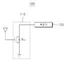
도 1은 본 발명의 일 실시예와 관련된 고속 데이터 출력용 테라헤르츠 수신기를 설명하기 위한 도면이다.
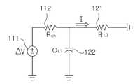
도 2는 본 발명의 일 실시예와 관련된 고속 데이터 출력용 테라헤르츠 수신기의 등가회로를 설명하기 위한 도면이다.
도 3은 본 발명의 일 실시예와 관련된 고속 데이터 출력용 테라헤르츠 이미징 센서 장치를 설명하기 위한 도면이다.
도 4는 본 발명의 일 실시예와 관련된 전압제어 발진기를 설명하기 위한 도면이다.
도 5은 전압제어 발진기의 이득(KVCO)을 설명하기 위한 그래프이다.
도 6은 본 발명의 전압제어 발진기의 출력 주파수를 시간에 따라 도시한 도면이다.
도 7은 본 발명의 일 실시예와 관련된 이미징 센서 장치의 구동 방법을 설명하기 위한 도면이다.1 is a diagram for explaining a terahertz receiver for high-speed data output according to an embodiment of the present invention.
2 is a diagram for explaining an equivalent circuit of a terahertz receiver for high-speed data output according to an embodiment of the present invention.
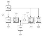
3 is a view for explaining a terahertz imaging sensor device for high-speed data output according to an embodiment of the present invention.
4 is a view for explaining a voltage-controlled oscillator according to an embodiment of the present invention.
5 is a graph for explaining the gain (KVCO) of the voltage-controlled oscillator.
6 is a graph showing the output frequency of the voltage-controlled oscillator of the present invention with time.
7 is a view for explaining a driving method of an imaging sensor device according to an embodiment of the present invention.
아래에서는 첨부한 도면을 참고로 하여 본 발명의 실시예에 대하여 본 발명이 속하는 기술 분야에서 통상의 지식을 가진 자가 용이하게 실시할 수 있도록 상세히 설명한다. 그러나 본 발명은 여러 가지 상이한 형태로 구현될 수 있으며 여기에서 설명하는 실시예에 한정되지 않는다. 그리고 도면에서 본 발명을 명확하게 설명하기 위해서 설명과 관계없는 부분은 생략하였으며, 명세서 전체를 통하여 유사한 부분에 대해서는 유사한 도면 부호를 붙였다.Hereinafter, embodiments of the present invention will be described in detail with reference to the accompanying drawings so that those skilled in the art can easily carry out the present invention. The present invention may, however, be embodied in many different forms and should not be construed as limited to the embodiments set forth herein. In order to clearly illustrate the present invention, parts not related to the description are omitted, and similar parts are denoted by like reference characters throughout the specification.
명세서 전체에서, 어떤 부분이 어떤 구성요소를 "포함"한다고 할 때, 이는 특별히 반대되는 기재가 없는 한 다른 구성요소를 제외하는 것이 아니라 다른 구성요소를 더 포함할 수 있는 것을 의미한다. 또한, 명세서에 기재된 "부", "기", "모듈" 등의 용어는 적어도 하나의 기능이나 동작을 처리하는 단위를 의미하며, 이는 하드웨어나 소프트웨어 또는 하드웨어 및 소프트웨어의 결합으로 구현할 수 있다.Throughout the specification, when an element is referred to as "comprising ", it means that it can include other elements as well, without excluding other elements unless specifically stated otherwise. Also, the terms "part," "module," and the like, which are described in the specification, refer to a unit for processing at least one function or operation, and may be implemented by hardware or software or a combination of hardware and software.
도 1은 본 발명의 일 실시예와 관련된 고속 데이터 출력용 테라헤르츠 수신기를 설명하기 위한 도면이다.1 is a diagram for explaining a terahertz receiver for high-speed data output according to an embodiment of the present invention.
도 1을 참조하면, 고속 데이터 출력용 테라헤르츠 수신기(100)는 검출기(110) 및, 측정기(120)를 포함할 수 있다.Referring to FIG. 1, a
검출기(110)는 수신 안테나를 통해 수신된 테라헤르츠파 신호를 전류로 변환할 수 있다. 검출기(110)는 테라헤르츠파 신호를 전류로 변환할 수 있는 전계효과트랜지스터(FET)를 구비할 수 있다.The
측정기(120)는 검출기(110)로부터 출력되는 전류를 읽을(readout) 수 있다. 예를 들면, 측정기(120)는 검출기(110)로부터 출력되는 전류를 전압으로 변환 및 증폭하는 트랜스임피던스(trans-impedance) 증폭기로 구현될 수 있다. 측정기(120)는 이외에도 다양한 형태로 구현될 수 있다.The
*도 2는 본 발명의 일 실시예와 관련된 고속 데이터 출력용 테라헤르츠 수신기의 등가회로를 설명하기 위한 도면이다.2 is a diagram for explaining an equivalent circuit of a terahertz receiver for high-speed data output according to an embodiment of the present invention.
도 2를 참조하면, 고속 데이터 출력용 테라헤르츠 수신기(100)는 검출기(110) 및, 측정기(120)를 포함할 수 있다.Referring to FIG. 2, the
검출기(110)는 테라헤르츠파에 의해 생성되는 트랜지스터의 DC 출력 전압(△V)(111) 및, 트랜지스터의 소스와 드레인 사이의 채널 저항(Rch)(112)과 같은 등가 회로로 표현될 수 있다.The
측정기(120)는 검출기(110)와 접지 사이에 연결되는 로드 저항(RLI)(121), 검출기(110)와 접지 사이에 연결되는 로드 기생 캐패시터(CLI)(122)과 같은 등가 회로로 표현될 수 있다.The
측정기(120)는 아래의 수학식을 이용하여 로드 저항(121)에 흐르는 전류를 측정할 수 있다.The measuring
* I = 1 / (Rch+ RLI|| CLI) * △V * (1/ωCLI / (1/ωCLI + RLI))* I = 1 / (Rch + RLI || CLI ) * DELTA V * (1 /? CLI / (1 /? CLI + RLI )
여기서, I : 로드 저항을 흐르는 전류Here, I represents the current flowing through the load resistance
△V : 테라헤르츠파에 의해 생성되는 트랜지스터의 DC 출력 전압 DELTA V: DC output voltage of the transistor generated by the terahertz wave
Rch: 트랜지스터의 소스와 드레인 사이의 채널 저항Rch : Channel resistance between source and drain of transistor
RLI: 측정기의 로드 저항RLI : Load resistance of measuring instrument
CLI: 측정기의 로드 기생 캐패시터CLI : Load parasitic capacitor of measuring instrument
테라헤르츠파에 의해 생성되는 트랜지스터의 DC 출력 전압(△V)을 최대한 전달하기 위해, 로드 저항(RLI)(121) 및, 로드 기생 캐패시터(CLI)는 작은 값을 사용한다. 예를 들면, 로드 저항(RLI)(121)는 1K를 사용하고, 로드 기생 캐패시터(CLI)(122)는 10fF을 사용할 수 있다. 모듈레이션(modulation) 주파수의 값이 증가하면, 로드 기생 캐패시터(CLI)의 임피던스 값은 작아진다. 로드 기생 캐패시터(CLI)(122)가 10fF인 경우, 모듈레이션 주파수와 로드 기생 캐패시터(CLI)의 임피던스 값의 관계는 아래 표 1과 같이 표현될 수 있다.The load resistance (RLI ) 121 and the load parasitic capacitor (CLI ) use a small value to maximally transfer the DC output voltage (? V) of the transistor generated by the terahertz wave. For example, 1 K is used for the load resistance (RLI ) 121 and 10 fF for the load parasitic capacitor (CLI ) 122. When the value of the modulation frequency increases, the impedance value of the load parasitic capacitor CLI becomes small. When the load parasitic capacitor (CLI ) 122 is 10 fF, the relationship between the modulation frequency and the impedance value of the load parasitic capacitor (CLI ) can be expressed as shown in Table 1 below.
위의 수학식을 참고하면, 측정기(120)의 로드 저항(RLI)(121)이 작은 값을 가지기 때문에, 측정되는 전류값은 모듈레이션(modulation) 주파수에 따라 로드 기생 캐패시터(CLI)의 임피던스의 값이 많이 변화되더라고, 크게 변화되지 않는다. 즉, 반응도의 변화가 작다. 따라서, 본 발명에 따른 측정기(120)는 광대역 테라헤르츠 통신에 적합하다.Since the load resistance (RLI ) 121 of the measuring
고속 데이터 출력용 테라헤르츠 수신기는 모듈레이션 주파수 변화에 따른 커패시터의 임피던스 변화를 적게 함으로써, 반응도의 변화를 작게 할 수 있다.The terahertz receiver for high-speed data output can reduce the variation of the impedance by changing the impedance of the capacitor according to the modulation frequency change.
도 3은 본 발명의 일 실시예와 관련된 고속 데이터 출력용 테라헤르츠 이미징 센서 장치를 설명하기 위한 도면이다.3 is a view for explaining a terahertz imaging sensor device for high-speed data output according to an embodiment of the present invention.
도 3을 참조하면, 고속 데이터 출력용 테라헤르츠 이미징 센서 장치는 검출기(200), 측정기(210), 디지털 신호 생성부(220), 조절기(225), 디지털 신호 처리기(230) 및 클록 생성부(235)를 포함할 수 있다.3, the terahertz imaging sensor device for high-speed data output includes a
검출기(200)는 수신 안테나를 통해 수신된 테라헤르츠파 신호를 전류로 변환할 수 있다. 검출기(200)는 테라헤르츠파 신호를 전류로 변환할 수 있는 전계효과트랜지스터(FET)를 구비할 수 있다.The
측정기(210)는 검출기(200)로부터 출력되는 전류를 읽을(readout) 수 있다. 예를 들면, 측정기(210)는 검출기(200)로부터 출력되는 전류를 전압으로 변환 및 증폭하는 트랜스임피던스(trans-impedance) 증폭기로 구현될 수 있다.The
측정기(210)는 도 1에 기재된 수학식을 이용하여 로드 저항에 흐르는 전류를 측정할 수 있다.The measuring
전압 제어 발진기(221)는 트랜스임피던스(trans-impedance) 증폭기(210)의 출력 전압에 따라 발진 주파수를 출력할 수 있다.The voltage-controlled
주파수 디지털 변환기(222)는 전압제어 발진기(221)로부터 출력된 발진 주파수를 디지털 신호로 변환할 수 있다. 예를 들면, 주파수 디지털 변환기(222)는 계수기 등으로 구현할 수 있다.The frequency
조절기(225)는 전압제어 발진기(221)에 인가되는 출력 전압을 조절하여 전압제어 발진기의 이득을 조절할 수 있다. 전압제어 발진기의 이득(KVCO) = (주파수 제어 범위) / (전압 제어 범위) 값이다.The
조절기(225)는 시스템의 상황이 출력 감도를 높여야할 경우, 전압제어 발진기의 이득이 높아지도록 전압제어 발진기(221)에 인가되는 출력 전압을 조절할 수 있다. 이에, 작은 출력 전압의 변화에도 전압제어 발진기(225)의 출력 주파수의 변화가 커지게 되므로, 출력 감도가 높아진다.The
반대로, 조절기(225)는 잡음의 민감도를 줄여야할 경우, 전압제어 발진기의 이득이 낮아지도록 전압제어 발진기(221)로 인가되는 출력 전압을 조절할 수 있다. 이에, 작은 출력 전압의 변화에도 전압제어 발진기(221)의 출력 주파수의 변화가 크지 않게 되므로, 출력이 잡음에 대해 민감하게 반응하지 않는다.Conversely, if the sensitivity of the noise is to be reduced, the
이와 같은 출력 전압의 조절은 사용자 등에 의한 수동 조절 또는 알고리즘 등을 통한 자동 조절이 가능하다.The output voltage can be adjusted manually by the user or by an algorithm.
디지털 신호 처리기(230)는 변환된 디지털 신호에 기초하여 데이터를 생성할 수 있다.The
디지털 신호 처리기(230)는 제 1 제어 신호가 검출기에 입력되는 동안 상기 전압제어 발진기(221)에서 생성된 제 1 발진 주파수와, 제 2 제어 신호가 검출기(200)에 입력되는 동안 상기 전압제어 발진기에서 생성된 제 2 발진 주파수의 차이 값에 기초하여 데이터를 생성할 수 있다. 전압제어 발진기(221)에서 생성된 제 1 발진 주파수 및 제 2 발진 주파수는 주파수 디지털 변환기(222)에서 디지털 신호로 변환되어 디지털 신호 처리기(230)로 입력될 수 있다.The
클록 생성부(235)는 초점면 배열 이미징 장치에 포함된 회로들의 동작을 위한 클록을 생성하고, 각 회로들의 동작 타이밍을 제어할 수 있다.The
예를 들면, 수신 안테나 및, 검출기(200)로 구성된 1개의 세트('1개의 픽셀에 대응')가 구성된 경우를 가정하면, 클록 생성부(235)는 1개의 세트를 구동하는 시간 동안, 검출기(200)에 제 1 제어 신호 및, 제 2 제어 신호를 입력할 수 있다. 여기서, 제 1 제어 신호는 수신된 테라헤르츠파에 의한 DC 출력 전류를 생성하도록 하는 신호이며, 제 2 제어 신호는 수신된 테라헤르츠파에 의한 DC 출력 전류를 생성하지 않도록 하는 신호이다. 여기서, 구동하는 시간 동안 검출기(200)에 전원은 항상 인가되어 있으며, 제 1 제어 신호는 검출기(200)가 수신된 테라헤르츠파에 의한 DC 출력 전류를 생성하도록 하고, 제 2 제어 신호는 수신된 테라헤르츠파에 의한 DC 출력 전류를 생성하지 않도록 제어하는 신호를 의미한다. 예를 들면, 검출기(200)가 전계효과 트랜지스터 검출기인 경우, 제 1 제어 전압 및 제 2 제어 전압은 바이어스 전압일 수 있다. 구동하는 시간이란 1개의 픽셀(pixel)에 대응되는 세트에 전원을 온(on) 시키는 시각으로부터 오프(off) 시키는 시각 사이의 시간을 의미한다. 구동하는 시간을 다른 용어로 스캔하는 시간이라고도 한다.For example, when it is assumed that a receiving antenna and a set of detectors 200 (corresponding to 'one pixel') are configured, the
도 4는 본 발명의 일 실시예와 관련된 전압제어 발진기를 설명하기 위한 도면이다.4 is a view for explaining a voltage-controlled oscillator according to an embodiment of the present invention.
도 4를 참조하면, 전압제어 발진기는 복수 개의 딜레이 셀이 직렬 연결된 링 형태로 구현된 링 전압제어 발진기일 수 있다. 예를 들면, 딜레이셀은 인버터(400, 410, 420, 430) 또는 차동 딜레이 셀 등으로 구현될 수 있다.Referring to FIG. 4, the voltage-controlled oscillator may be a ring voltage-controlled oscillator implemented in the form of a ring in which a plurality of delay cells are connected in series. For example, the delay cell may be implemented as an
딜레이 셀은 인가되는 전압에 의해 전류를 제어하여 RC 시정수 제어가 가능하도록 구현된다.The delay cell is configured to control the RC time constant by controlling the current by the applied voltage.
이에, 복수 개의 딜레이 셀로 이루어진 전압제어 발진기는 검출기의 출력 전압(Vctrl)을 입력 받아 그에 따른 발진 주파수(fOSC)를 출력한다.Thus, the voltage-controlled oscillator including a plurality of delay cells receives the output voltage Vctrl of the detector and outputs the oscillation frequency fOSC corresponding thereto.
도 5은 전압제어 발진기의 이득(KVCO)을 설명하기 위한 그래프이다.5 is a graph for explaining the gain (KVCO) of the voltage-controlled oscillator.
도 5에는 전압제어 발진기의 제어 전압(Vctrl)에 따른 출력 주파수(fOSC) 곡선이다. 전압제어 발진기의 이득(KVCO) = (주파수 제어 범위) / (전압 제어 범위) 값이다.5 is an output frequency (fOSC ) curve according to the control voltage Vctrl of the voltage-controlled oscillator. The gain of the voltage-controlled oscillator (KVCO) = (frequency control range) / (voltage control range).
따라서, 전압제어 발진기(KVCO)의 정의에 따라 도 3의 곡선의 기울기가 각 제어 전압(Vctrl)에 대한 전압제어 발진기(KVCO) 값이 된다. 곡선의 기울기가 높은 부분이 high KVCO 부분이 되고, 곡선의 기울기가 낮은 부분이 low KVCO 부분이 된다.Therefore, according to the definition of the voltage-controlled oscillator KVCO, the slope of the curve of FIG. 3 becomes the voltage-controlled oscillator (KVCO) value for each control voltage Vctrl. The high slope part of the curve becomes the high KVCO part and the low slope part of the curve becomes the low KVCO part.
시스템의 상황이 출력 감도를 높여야할 경우, 전압제어 발진기의 이득이 높아지도록 전압제어 발진기에 인가되는 출력 전압을 조절(출력 전압을 high KVCO 부분으로 이동시킴)할 수 있다.If the system needs to increase the output sensitivity, the output voltage applied to the voltage controlled oscillator can be adjusted (the output voltage is shifted to the high KVCO portion) so that the gain of the voltage controlled oscillator is increased.
반대로, 잡음의 민감도를 줄여야할 경우, 전압제어 발진기의 이득이 낮아지도록 전압제어 발진기로 인가되는 출력 전압을 조절(출력 전압을 low KVCO 부분으로 이동시킴)할 수 있다.Conversely, if the sensitivity of the noise is to be reduced, the output voltage applied to the voltage controlled oscillator can be regulated (the output voltage is shifted to the low KVCO portion) so that the gain of the voltage controlled oscillator is reduced.
이와 같이, 시스템의 상황에 맞게 출력 전압을 조절함으로써, 전압제어 발진기는 최적의 상황에서 발진 주파수를 출력할 수 있다.Thus, by adjusting the output voltage according to the system conditions, the voltage-controlled oscillator can output the oscillation frequency under optimum conditions.
도 6은 본 발명의 전압제어 발진기의 출력 주파수를 시간에 따라 도시한 도면이다.6 is a graph showing the output frequency of the voltage-controlled oscillator of the present invention with time.
도 6에 기재된 그래프의 가로축은 시간이며, 세로축은 전압제어 발진기에서 생성되는 출력 주파수이다.The abscissa of the graph shown in Fig. 6 is the time, and the ordinate is the output frequency generated by the voltage-controlled oscillator.
도 5 및 도 6을 참조하면, t1, t3, t5, t7 등의 시간에 제 1 제어 신호가 입력되는 경우 또는 t2, t4, t6, t7 등의 시간에 제 1 제어 신호가 입력되는 경우에 전압제어 발진기에서 출력된 주파수의 절대값을 보면 일정하지 않다. 이와 같이 전압 제어 발진기의 출력 주파수가 일정하지 않은 이유는 주파수 드리프트(frequency drift) 현상 때문이다.5 and 6, when a first control signal is input at times t1, t3, t5, t7, or the like, or when a first control signal is input at times t2, t4, t6, The absolute value of the frequency output from the controlled oscillator is not constant. The reason why the output frequency of the voltage controlled oscillator is not constant is due to the frequency drift phenomenon.
본 발명에 따른 디지털 신호 처리기는 전압제어 발진기에서 출력된 주파수의 절대값을 이용하지 않고, 제 1 제어 신호가 검출기에 입력되는 동안 전압제어 발진기에서 생성된 제 1 발진 주파수와, 제 2 제어 신호가 검출기에 입력되는 동안 전압제어 발진기에서 생성된 제 2 발진 주파수의 차이 값('△f')을 이용함으로써, 주파수 드리프트(frequency drift) 현상에 따른 노이즈를 없앨 수 있다. 여기서, △f는 제 1 제어 신호가 입력된 경우의 인가 전압과 제 2 제어 신호가 입력된 경우의 인가 전압의 차이값인 △V에 의해 발생되는 출력 주파수의 차이값일 수 있다.The digital signal processor according to the present invention does not use the absolute value of the frequency output from the voltage controlled oscillator but uses the first oscillation frequency generated by the voltage controlled oscillator while the first control signal is inputted to the detector, By using the difference value (? F ') of the second oscillation frequency generated by the voltage-controlled oscillator during the input to the detector, it is possible to eliminate the noise due to the frequency drift phenomenon. Here,? F may be a difference value of the output frequency generated by? V, which is a difference value between the applied voltage when the first control signal is input and the applied voltage when the second control signal is input.
도 7은 본 발명의 일 실시예와 관련된 이미징 센서 장치의 구동 방법을 설명하기 위한 도면이다.7 is a view for explaining a driving method of an imaging sensor device according to an embodiment of the present invention.
이하에서는 이미징 센서 장치가 4개의 픽셀(pixel)로 구성되어 있고, 4개의 픽셀에 대응되는 세트(수신 안테나 및 검출기를 포함)가 4개 존재하는 경우를 기준으로 설명하겠다. 그러나, 이미징 센서 장치에 포함된 픽셀의 개수는 이에 한정되지 않고 다양하게 구현될 수 있다.Hereinafter, the case where the imaging sensor apparatus is composed of four pixels and four sets (including a receiving antenna and a detector) corresponding to four pixels are present will be described. However, the number of pixels included in the imaging sensor device is not limited to this, and may be variously implemented.
도 3 및 도 7을 참조하면, 세트 1, 세트 2, 세트 3 및 세트 4에는 구동 신호가 순차적으로 인가될 수 있다. 예를 들면, 각 구동 신호는 2ms 동안 인가될 수 있다.Referring to FIGS. 3 and 7, driving signals may be sequentially applied to the
클록 생성부(235)는 각각의 세트 1, 세트 2, 세트 3 및 세트 4들을 구동하는 시간 동안, 제 1 제어 신호 및 제 2 제어 신호를 생성하여 검출기(200)에 입력할 수 있다. 여기서, 제 1 제어 신호는 수신된 테라헤르츠파에 의한 DC 출력 전압을 생성하도록 하는 신호이며, 제 2 제어 신호는 수신된 테라헤르츠파에 의한 DC 출력 전압을 생성하지 않도록 하는 신호이다. 제 1 제어 신호 및 제 2 제어신호의 인가 시간은 각각 1ms이다.The
디지털 신호 처리기(230)는 제 1 제어 신호가 검출기에 입력되는 동안 전압제어 발진기(221)에서 생성된 제 1 발진 주파수를 읽어 들이고, 제 2 제어 신호가 검출기에 입력되는 동안 상기 전압제어 발진기에서 생성된 제 2 발진 주파수를 읽어 들일 수 있다. 예를 들면, 디지털 신호 처리기(230)는 제 1 제어 신호가 입력되는 '1ms' 내에, 전압제어 발진기(221)에서 생성된 제 1 발진 주파수를 읽어('리딩 신호')들이고, 제 2 제어 신호가 입력되는 '1ms' 내에, 전압제어 발진기(221)에서 생성된 제 2 발진 주파수를 읽어('리딩 신호') 들일 수 있다. 즉, 디지털 신호 처리기(230)는 리딩 신호('1ms') 마다 발진 주파수를 읽어 들일 수 있다.The
예를 들면, 디지털 신호 처리기(230)는 제 1 제어 신호 또는 제 2 제어 신호가 검출기에 입력되었다가 없어 질 때 또는, 리딩 신호가 입력될 때, 직전 '1ms' 동안에 생성된 발진 주파수를 읽을 수 있다. 구체적으로는, 주파수 디지털 변환기(222)는 직전 '1ms' 동안 전압 제어 발진기(221)에서 생성된 발진 주파수를 읽어들이고, 디지털 신호 처리기(230)는 주파수 디지털 변환기(222)에서 생성된 발진 주파수 신호를 읽을 수 있다.For example, the
예를 들면, 디지털 신호 처리기(230)는 세트에 인가되는 구동 신호의 하강 에지(falling) 마다 제 1 발진 주파수 및, 제 2 발진 주파수의 차이값(△f)를 연산할 수 있다.For example, the
디지털 신호 처리기(230)는 읽어들인 제 1 발진 주파수와 제 2 발진 주파수의 차이 값에 기초하여 데이터를 생성할 수 있다.The
설명된 실시예들은 다양한 변형이 이루어질 수 있도록 각 실시예들의 전부 또는 일부가 선택적으로 조합되어 구성될 수도 있다.The embodiments described may be constructed by selectively combining all or a part of each embodiment so that various modifications can be made.
또한, 실시예는 그 설명을 위한 것이며, 그 제한을 위한 것이 아님을 주의하여야 한다. 또한, 본 발명의 기술분야의 통상의 전문가라면 본 발명의 기술사상의 범위에서 다양한 실시예가 가능함을 이해할 수 있을 것이다.It should also be noted that the embodiments are for explanation purposes only, and not for the purpose of limitation. In addition, it will be understood by those of ordinary skill in the art that various embodiments are possible within the scope of the technical idea of the present invention.
100 : 고속 데이터 출력용 테라헤르츠 수신기
111 : 트랜지스터의 DC 출력 전압
112 : 채널 저항
110 : 검출기
120 : 측정기
121 : 로드 저항
122 : 로드 기생 캐패시터
200 : 검출기
210 : 측정기
220 : 디지털 신호 생성부
225 : 조절기
230 : 디지털 신호 처리기
235 : 클록 생성부100: Terahertz receiver for high-speed data output
111: DC output voltage of the transistor
112: Channel resistance
110: detector
120: Measuring instrument
121: Load resistance
122: load parasitic capacitor
200: detector
210: Meter
220: Digital Signal Generation Unit
225: regulator
230: Digital Signal Processor
235: clock generation unit
Claims (4)
Translated fromKorean상기 검출기와 접지 사이에 연결되는 로드 저항과 상기 검출기와 접지 사이에 연결되는 로드 기생 캐패시터를 포함하고, 상기 검출기로부터 출력되는 상기 로드 저항에 흐르는 전류를 아래의 수학식을 이용하여 읽는 측정기를 포함하는,
I = 1 / (Rch+ RLI|| CLI) * △V * (1/ωCLI / (1/ωCLI + RLI))
여기서, I : 로드 저항을 흐르는 전류
△V : 테라헤르츠파에 의해 생성되는 트랜지스터의 DC 출력 전압
Rch: 트랜지스터의 소스와 드레인 사이의 채널 저항
RLI: 측정기의 로드 저항
CLI: 측정기의 로드 기생 캐패시터
고속 데이터 출력용 테라헤르츠 수신기.
A detector having a field effect transistor (FET) for converting a terahertz wave signal received via a receive antenna into a current; And
And a load parasitic capacitor connected between the detector and ground, and a load parasitic capacitor connected between the detector and ground, wherein the meter reads the current flowing in the load resistor output from the detector using the following equation ,
I = 1 / (Rch + RLI || CLI ) * DELTA V * (1 /? CLI / (1 /? CLI + RLI )
Here, I represents the current flowing through the load resistance
DELTA V: DC output voltage of the transistor generated by the terahertz wave
Rch : Channel resistance between source and drain of transistor
RLI : Load resistance of measuring instrument
CLI : Load parasitic capacitor of measuring instrument
Terahertz receiver for high-speed data output.
상기 검출기와 접지 사이에 연결되는 로드 저항과 상기 검출기와 접지 사이에 연결되는 로드 기생 캐패시터를 포함하고, 상기 검출기로부터 출력되는 상기 로드 저항에 흐르는 전류를 읽으며, 상기 검출기로부터 출력되는 전류를 전압으로 변환 및 증폭하는 트랜스임피던스 증폭기로 구성되는 측정기;
상기 측정기의 출력 전압에 따라 발진 주파수를 출력하는 전압 제어 발진기와, 상기 전압 제어 발진기로부터 출력된 발진 주파수를 디지털 신호로 변환하는 주파수 디지털 변환기를 포함하고, 상기 측정기에서 측정된 전류 값에 기초하여 디지털 신호를 생성하는 디지털 신호 생성부; 및
수신안테나 및 상기 검출기를 포함하는 세트를 구동하는 시간 동안, 상기 검출기에 상기 수신된 테라헤르츠파에 의한 DC 출력 전류를 생성하도록 하는 제 1 제어 신호 및, 상기 수신된 테라헤르츠파에 의한 DC 출력 전류를 생성하지 않도록 하는 제 2 제어 신호를 입력하는 클록 생성부; 및
상기 제 1 제어 신호가 검출기에 입력되는 동안 상기 전압 제어 발진기에서 생성된 제 1 발진 주파수와, 상기 제 2 제어 신호가 검출기에 입력되는 동안 상기 전압 제어 발진기에서 생성된 제 2 발진 주파수의 차이 값에 기초하여 데이터를 생성하는 디지털 신호처리기;를 포함하는, 고속 데이터 출력용 테라헤르츠 이미징 센서 장치.
A detector having a field effect transistor (FET) for converting a terahertz wave signal received via a receive antenna into a current;
A load resistor connected between the detector and ground, and a load parasitic capacitor connected between the detector and ground, wherein the current flowing in the load resistor output from the detector is read, and the current output from the detector is converted into a voltage And a transimpedance amplifier for amplifying the signal;
A voltage-controlled oscillator for outputting an oscillation frequency in accordance with an output voltage of the measuring device; and a frequency-to-digital converter for converting the oscillation frequency output from the voltage-controlled oscillator into a digital signal, A digital signal generation unit for generating a signal; And
A first control signal for causing the detector to generate a DC output current due to the received terahertz wave during a time for driving the set including the receiving antenna and the detector and a second control signal for causing the detector to generate a DC output current by the received terahertz wave A clock generator for inputting a second control signal for not generating the second control signal; And
A first oscillation frequency generated by the voltage control oscillator while the first control signal is input to the detector and a second oscillation frequency generated by the voltage control oscillator while the second control signal is input to the detector And a digital signal processor for generating data on the basis of the received signal.
상기 전압 제어 발진기에 인가되는 상기 출력 전압을 조절하여 전압제어 발진기의 이득을 조절하고, 출력 감도를 높여야 할 경우 상기 전압제어 발진기의 이득이 높아지도록 상기 측정기의 출력 전압을 조절하고, 잡음의 민감도를 줄여야 할 경우 상기 전압제어 발진기의 이득이 낮아지도록 상기 출력 전압을 조절하는 조절기를 더 포함하는, 고속 데이터 출력용 테라헤르츠 이미징 센서 장치.
3. The method of claim 2,
The output voltage of the voltage controlled oscillator is adjusted to adjust the gain of the voltage controlled oscillator and the output voltage of the voltage controlled oscillator is adjusted to increase the output sensitivity when the output sensitivity is to be increased, Further comprising: a regulator for regulating the output voltage such that the gain of the voltage controlled oscillator is reduced when the output voltage of the voltage controlled oscillator is reduced.
상기 측정기는 아래의 수학식을 이용하여 전류를 읽는,
I = 1 / (Rch+ RLI|| CLI) * △V * (1/ωCLI / (1/ωCLI + RLI))
여기서, I : 로드 저항을 흐르는 전류
△V : 테라헤르츠파에 의해 생성되는 트랜지스터의 DC 출력 전압
Rch: 트랜지스터의 소스와 드레인 사이의 채널 저항
RLI: 측정기의 로드 저항
CLI: 측정기의 로드 기생 캐패시터
고속 데이터 출력용 테라헤르츠 이미징 센서 장치.3. The method of claim 2,
The measuring device reads the current using the following equation: < EMI ID =
I = 1 / (Rch + RLI || CLI ) * DELTA V * (1 /? CLI / (1 /? CLI + RLI )
Here, I represents the current flowing through the load resistance
DELTA V: DC output voltage of the transistor generated by the terahertz wave
Rch : Channel resistance between source and drain of transistor
RLI : Load resistance of measuring instrument
CLI : Load parasitic capacitor of measuring instrument
Terahertz imaging sensor device for high speed data output.
Priority Applications (1)
| Application Number | Priority Date | Filing Date | Title |
|---|---|---|---|
| KR1020160104287AKR101675977B1 (en) | 2016-08-17 | 2016-08-17 | Terahertz receiver and terahertz imaginig sensor apparatus for high data rate |
Applications Claiming Priority (1)
| Application Number | Priority Date | Filing Date | Title |
|---|---|---|---|
| KR1020160104287AKR101675977B1 (en) | 2016-08-17 | 2016-08-17 | Terahertz receiver and terahertz imaginig sensor apparatus for high data rate |
Related Parent Applications (1)
| Application Number | Title | Priority Date | Filing Date |
|---|---|---|---|
| KR1020150009328Division | 2015-01-20 | 2015-01-20 |
Publications (2)
| Publication Number | Publication Date |
|---|---|
| KR20160102367A KR20160102367A (en) | 2016-08-30 |
| KR101675977B1true KR101675977B1 (en) | 2016-11-15 |
Family
ID=56886107
Family Applications (1)
| Application Number | Title | Priority Date | Filing Date |
|---|---|---|---|
| KR1020160104287AActiveKR101675977B1 (en) | 2016-08-17 | 2016-08-17 | Terahertz receiver and terahertz imaginig sensor apparatus for high data rate |
Country Status (1)
| Country | Link |
|---|---|
| KR (1) | KR101675977B1 (en) |
Families Citing this family (3)
| Publication number | Priority date | Publication date | Assignee | Title |
|---|---|---|---|---|
| KR102113259B1 (en)* | 2018-11-06 | 2020-05-20 | 영남대학교 산학협력단 | Power detector with wide dynamic range |
| KR102483252B1 (en)* | 2019-10-31 | 2023-01-03 | 동국대학교 산학협력단 | Amplifier of terahertz band, method for design the same, and radiator with the same |
| WO2021086113A1 (en)* | 2019-10-31 | 2021-05-06 | 동국대학교 산학협력단 | Amplifier of terahertz band, method for designing same, and radiator with same |
Citations (2)
| Publication number | Priority date | Publication date | Assignee | Title |
|---|---|---|---|---|
| JP2003289259A (en) | 2002-01-22 | 2003-10-10 | Matsushita Electric Ind Co Ltd | High frequency signal receiving device and method of manufacturing the same |
| JP2011509518A (en) | 2007-12-22 | 2011-03-24 | ヨハン ヴォルフガング ゲーテ−ウニヴェルジテート フランクフルト アム マイン | Monolithic integrated antenna and receiver circuit for detecting terahertz waves |
Family Cites Families (1)
| Publication number | Priority date | Publication date | Assignee | Title |
|---|---|---|---|---|
| GB8728853D0 (en)* | 1987-12-10 | 1988-01-27 | Bt & D Technologies Ltd | Transimpedance pre-amplifier & receiver including pre-amplifier |
- 2016
- 2016-08-17KRKR1020160104287Apatent/KR101675977B1/enactiveActive
Patent Citations (2)
| Publication number | Priority date | Publication date | Assignee | Title |
|---|---|---|---|---|
| JP2003289259A (en) | 2002-01-22 | 2003-10-10 | Matsushita Electric Ind Co Ltd | High frequency signal receiving device and method of manufacturing the same |
| JP2011509518A (en) | 2007-12-22 | 2011-03-24 | ヨハン ヴォルフガング ゲーテ−ウニヴェルジテート フランクフルト アム マイン | Monolithic integrated antenna and receiver circuit for detecting terahertz waves |
Also Published As
| Publication number | Publication date |
|---|---|
| KR20160102367A (en) | 2016-08-30 |
Similar Documents
| Publication | Publication Date | Title |
|---|---|---|
| US10684170B2 (en) | Terahertz spectroscopy system and method | |
| US20160209268A1 (en) | Terahertz receiver and terahertz imaging sensor apparatus for high data rate | |
| KR101675977B1 (en) | Terahertz receiver and terahertz imaginig sensor apparatus for high data rate | |
| Hisatake et al. | Self-heterodyne spectrometer using uni-traveling-carrier photodiodes for terahertz-wave generators and optoelectronic mixers | |
| US4433238A (en) | Optical measurement system for spectral analysis | |
| JP2004077479A (en) | System and method for laser ranging | |
| GB2586075A (en) | Rapidly tuneable diode lidar | |
| US10432205B2 (en) | Quantum interference device, atomic oscillator, and electronic apparatus | |
| JP4719383B2 (en) | Local oscillator and method of using the same | |
| Boiko et al. | Mid-infrared two photon absorption sensitivity of commercial detectors | |
| Demers et al. | An optically integrated coherent frequency-domain THz spectrometer with signal-to-noise ratio up to 80 dB | |
| Lin et al. | A 4-D FMCW LiDAR with ultra-high velocity sensitivity | |
| US20180164211A1 (en) | Gas Detection Device and Gas Detection Method | |
| ATE352115T1 (en) | LASER SPECTROSCOPY USING A MASTER-SLAVE CONTROL ARCHITECTURE | |
| KR20180005447A (en) | APPARATUS FOR GENERATING THz WAVE USING PHASE MODULATION | |
| JP6753232B2 (en) | Atomic oscillators, electronics and mobiles | |
| CN113092411B (en) | Device and method for realizing self-stabilization of received light intensity based on laser array | |
| US10194806B2 (en) | System and method for measuring phase delay and amplitude of a near infra-red signal in animal tissue | |
| KR101533236B1 (en) | Imaging sensor apparatus and focal plane array apparatus using frequency conversion for real-time terahertz imaginig | |
| KR101092484B1 (en) | Terahertz spectrum analyzer | |
| Zheng et al. | A CMOS AFE array with DC input current cancellation for FMCW LiDAR | |
| KR20180005460A (en) | APPARATUS FOR GENERATING THz WAVE USING ACTIVE MODE LOCKING LASER | |
| RU2426226C1 (en) | Quantum frequency standard | |
| Rothbart et al. | Gas spectroscopy by voltage-frequency tuning of a 245 GHz SiGe transmitter and receiver | |
| JP2009080007A (en) | Time-resolved spectroscopic system, time-resolved spectroscopic method, and terahertz wave generation system |
Legal Events
| Date | Code | Title | Description |
|---|---|---|---|
| A107 | Divisional application of patent | ||
| A201 | Request for examination | ||
| PA0107 | Divisional application | Comment text:Divisional Application of Patent Patent event date:20160817 Patent event code:PA01071R01D Filing date:20150120 Application number text:1020150009328 | |
| PA0201 | Request for examination | ||
| E701 | Decision to grant or registration of patent right | ||
| PE0701 | Decision of registration | Patent event code:PE07011S01D Comment text:Decision to Grant Registration Patent event date:20160826 | |
| PG1501 | Laying open of application | ||
| GRNT | Written decision to grant | ||
| PR0701 | Registration of establishment | Comment text:Registration of Establishment Patent event date:20161108 Patent event code:PR07011E01D | |
| PR1002 | Payment of registration fee | Payment date:20161109 End annual number:3 Start annual number:1 | |
| PG1601 | Publication of registration | ||
| PR1001 | Payment of annual fee | Payment date:20201026 Start annual number:5 End annual number:5 | |
| PR1001 | Payment of annual fee | Payment date:20211101 Start annual number:6 End annual number:6 | |
| PR1001 | Payment of annual fee | Payment date:20221021 Start annual number:7 End annual number:7 | |
| PR1001 | Payment of annual fee | Payment date:20241024 Start annual number:9 End annual number:9 |