KR101672640B1 - Semiconductor device - Google Patents
Semiconductor deviceDownload PDFInfo
- Publication number
- KR101672640B1 KR101672640B1KR1020150089245AKR20150089245AKR101672640B1KR 101672640 B1KR101672640 B1KR 101672640B1KR 1020150089245 AKR1020150089245 AKR 1020150089245AKR 20150089245 AKR20150089245 AKR 20150089245AKR 101672640 B1KR101672640 B1KR 101672640B1
- Authority
- KR
- South Korea
- Prior art keywords
- conductive
- stiffener
- interposer
- layer
- semiconductor die
- Prior art date
- Legal status (The legal status is an assumption and is not a legal conclusion. Google has not performed a legal analysis and makes no representation as to the accuracy of the status listed.)
- Active
Links
Images


Classifications
- H—ELECTRICITY
- H01—ELECTRIC ELEMENTS
- H01L—SEMICONDUCTOR DEVICES NOT COVERED BY CLASS H10
- H01L24/00—Arrangements for connecting or disconnecting semiconductor or solid-state bodies; Methods or apparatus related thereto
- H01L24/93—Batch processes
- H01L24/95—Batch processes at chip-level, i.e. with connecting carried out on a plurality of singulated devices, i.e. on diced chips
- H01L24/97—Batch processes at chip-level, i.e. with connecting carried out on a plurality of singulated devices, i.e. on diced chips the devices being connected to a common substrate, e.g. interposer, said common substrate being separable into individual assemblies after connecting
- H—ELECTRICITY
- H01—ELECTRIC ELEMENTS
- H01L—SEMICONDUCTOR DEVICES NOT COVERED BY CLASS H10
- H01L23/00—Details of semiconductor or other solid state devices
- H01L23/562—Protection against mechanical damage
- H—ELECTRICITY
- H01—ELECTRIC ELEMENTS
- H01L—SEMICONDUCTOR DEVICES NOT COVERED BY CLASS H10
- H01L23/00—Details of semiconductor or other solid state devices
- H01L23/48—Arrangements for conducting electric current to or from the solid state body in operation, e.g. leads, terminal arrangements ; Selection of materials therefor
- H01L23/488—Arrangements for conducting electric current to or from the solid state body in operation, e.g. leads, terminal arrangements ; Selection of materials therefor consisting of soldered or bonded constructions
- H01L23/498—Leads, i.e. metallisations or lead-frames on insulating substrates, e.g. chip carriers
- H01L23/49822—Multilayer substrates
- H—ELECTRICITY
- H01—ELECTRIC ELEMENTS
- H01L—SEMICONDUCTOR DEVICES NOT COVERED BY CLASS H10
- H01L21/00—Processes or apparatus adapted for the manufacture or treatment of semiconductor or solid state devices or of parts thereof
- H01L21/70—Manufacture or treatment of devices consisting of a plurality of solid state components formed in or on a common substrate or of parts thereof; Manufacture of integrated circuit devices or of parts thereof
- H01L21/71—Manufacture of specific parts of devices defined in group H01L21/70
- H01L21/768—Applying interconnections to be used for carrying current between separate components within a device comprising conductors and dielectrics
- H01L21/76898—Applying interconnections to be used for carrying current between separate components within a device comprising conductors and dielectrics formed through a semiconductor substrate
- H—ELECTRICITY
- H01—ELECTRIC ELEMENTS
- H01L—SEMICONDUCTOR DEVICES NOT COVERED BY CLASS H10
- H01L23/00—Details of semiconductor or other solid state devices
- H01L23/48—Arrangements for conducting electric current to or from the solid state body in operation, e.g. leads, terminal arrangements ; Selection of materials therefor
- H01L23/481—Internal lead connections, e.g. via connections, feedthrough structures
- H—ELECTRICITY
- H01—ELECTRIC ELEMENTS
- H01L—SEMICONDUCTOR DEVICES NOT COVERED BY CLASS H10
- H01L23/00—Details of semiconductor or other solid state devices
- H01L23/48—Arrangements for conducting electric current to or from the solid state body in operation, e.g. leads, terminal arrangements ; Selection of materials therefor
- H01L23/488—Arrangements for conducting electric current to or from the solid state body in operation, e.g. leads, terminal arrangements ; Selection of materials therefor consisting of soldered or bonded constructions
- H01L23/498—Leads, i.e. metallisations or lead-frames on insulating substrates, e.g. chip carriers
- H01L23/49811—Additional leads joined to the metallisation on the insulating substrate, e.g. pins, bumps, wires, flat leads
- H—ELECTRICITY
- H01—ELECTRIC ELEMENTS
- H01L—SEMICONDUCTOR DEVICES NOT COVERED BY CLASS H10
- H01L23/00—Details of semiconductor or other solid state devices
- H01L23/52—Arrangements for conducting electric current within the device in operation from one component to another, i.e. interconnections, e.g. wires, lead frames
- H01L23/522—Arrangements for conducting electric current within the device in operation from one component to another, i.e. interconnections, e.g. wires, lead frames including external interconnections consisting of a multilayer structure of conductive and insulating layers inseparably formed on the semiconductor body
- H01L23/5226—Via connections in a multilevel interconnection structure
- H—ELECTRICITY
- H01—ELECTRIC ELEMENTS
- H01L—SEMICONDUCTOR DEVICES NOT COVERED BY CLASS H10
- H01L23/00—Details of semiconductor or other solid state devices
- H01L23/52—Arrangements for conducting electric current within the device in operation from one component to another, i.e. interconnections, e.g. wires, lead frames
- H01L23/522—Arrangements for conducting electric current within the device in operation from one component to another, i.e. interconnections, e.g. wires, lead frames including external interconnections consisting of a multilayer structure of conductive and insulating layers inseparably formed on the semiconductor body
- H01L23/525—Arrangements for conducting electric current within the device in operation from one component to another, i.e. interconnections, e.g. wires, lead frames including external interconnections consisting of a multilayer structure of conductive and insulating layers inseparably formed on the semiconductor body with adaptable interconnections
- H—ELECTRICITY
- H01—ELECTRIC ELEMENTS
- H01L—SEMICONDUCTOR DEVICES NOT COVERED BY CLASS H10
- H01L21/00—Processes or apparatus adapted for the manufacture or treatment of semiconductor or solid state devices or of parts thereof
- H01L21/02—Manufacture or treatment of semiconductor devices or of parts thereof
- H01L21/04—Manufacture or treatment of semiconductor devices or of parts thereof the devices having potential barriers, e.g. a PN junction, depletion layer or carrier concentration layer
- H01L21/48—Manufacture or treatment of parts, e.g. containers, prior to assembly of the devices, using processes not provided for in a single one of the groups H01L21/18 - H01L21/326 or H10D48/04 - H10D48/07
- H01L21/4814—Conductive parts
- H01L21/4846—Leads on or in insulating or insulated substrates, e.g. metallisation
- H01L21/4857—Multilayer substrates
- H—ELECTRICITY
- H01—ELECTRIC ELEMENTS
- H01L—SEMICONDUCTOR DEVICES NOT COVERED BY CLASS H10
- H01L21/00—Processes or apparatus adapted for the manufacture or treatment of semiconductor or solid state devices or of parts thereof
- H01L21/02—Manufacture or treatment of semiconductor devices or of parts thereof
- H01L21/04—Manufacture or treatment of semiconductor devices or of parts thereof the devices having potential barriers, e.g. a PN junction, depletion layer or carrier concentration layer
- H01L21/48—Manufacture or treatment of parts, e.g. containers, prior to assembly of the devices, using processes not provided for in a single one of the groups H01L21/18 - H01L21/326 or H10D48/04 - H10D48/07
- H01L21/4814—Conductive parts
- H01L21/4846—Leads on or in insulating or insulated substrates, e.g. metallisation
- H01L21/486—Via connections through the substrate with or without pins
- H—ELECTRICITY
- H01—ELECTRIC ELEMENTS
- H01L—SEMICONDUCTOR DEVICES NOT COVERED BY CLASS H10
- H01L2224/00—Indexing scheme for arrangements for connecting or disconnecting semiconductor or solid-state bodies and methods related thereto as covered by H01L24/00
- H01L2224/01—Means for bonding being attached to, or being formed on, the surface to be connected, e.g. chip-to-package, die-attach, "first-level" interconnects; Manufacturing methods related thereto
- H01L2224/10—Bump connectors; Manufacturing methods related thereto
- H01L2224/15—Structure, shape, material or disposition of the bump connectors after the connecting process
- H01L2224/16—Structure, shape, material or disposition of the bump connectors after the connecting process of an individual bump connector
- H01L2224/161—Disposition
- H01L2224/16151—Disposition the bump connector connecting between a semiconductor or solid-state body and an item not being a semiconductor or solid-state body, e.g. chip-to-substrate, chip-to-passive
- H01L2224/16221—Disposition the bump connector connecting between a semiconductor or solid-state body and an item not being a semiconductor or solid-state body, e.g. chip-to-substrate, chip-to-passive the body and the item being stacked
- H01L2224/16225—Disposition the bump connector connecting between a semiconductor or solid-state body and an item not being a semiconductor or solid-state body, e.g. chip-to-substrate, chip-to-passive the body and the item being stacked the item being non-metallic, e.g. insulating substrate with or without metallisation
- H01L2224/16227—Disposition the bump connector connecting between a semiconductor or solid-state body and an item not being a semiconductor or solid-state body, e.g. chip-to-substrate, chip-to-passive the body and the item being stacked the item being non-metallic, e.g. insulating substrate with or without metallisation the bump connector connecting to a bond pad of the item
- H—ELECTRICITY
- H01—ELECTRIC ELEMENTS
- H01L—SEMICONDUCTOR DEVICES NOT COVERED BY CLASS H10
- H01L2224/00—Indexing scheme for arrangements for connecting or disconnecting semiconductor or solid-state bodies and methods related thereto as covered by H01L24/00
- H01L2224/01—Means for bonding being attached to, or being formed on, the surface to be connected, e.g. chip-to-package, die-attach, "first-level" interconnects; Manufacturing methods related thereto
- H01L2224/26—Layer connectors, e.g. plate connectors, solder or adhesive layers; Manufacturing methods related thereto
- H01L2224/31—Structure, shape, material or disposition of the layer connectors after the connecting process
- H01L2224/32—Structure, shape, material or disposition of the layer connectors after the connecting process of an individual layer connector
- H01L2224/321—Disposition
- H01L2224/32151—Disposition the layer connector connecting between a semiconductor or solid-state body and an item not being a semiconductor or solid-state body, e.g. chip-to-substrate, chip-to-passive
- H01L2224/32221—Disposition the layer connector connecting between a semiconductor or solid-state body and an item not being a semiconductor or solid-state body, e.g. chip-to-substrate, chip-to-passive the body and the item being stacked
- H01L2224/32225—Disposition the layer connector connecting between a semiconductor or solid-state body and an item not being a semiconductor or solid-state body, e.g. chip-to-substrate, chip-to-passive the body and the item being stacked the item being non-metallic, e.g. insulating substrate with or without metallisation
- H—ELECTRICITY
- H01—ELECTRIC ELEMENTS
- H01L—SEMICONDUCTOR DEVICES NOT COVERED BY CLASS H10
- H01L2224/00—Indexing scheme for arrangements for connecting or disconnecting semiconductor or solid-state bodies and methods related thereto as covered by H01L24/00
- H01L2224/73—Means for bonding being of different types provided for in two or more of groups H01L2224/10, H01L2224/18, H01L2224/26, H01L2224/34, H01L2224/42, H01L2224/50, H01L2224/63, H01L2224/71
- H01L2224/732—Location after the connecting process
- H01L2224/73201—Location after the connecting process on the same surface
- H01L2224/73203—Bump and layer connectors
- H01L2224/73204—Bump and layer connectors the bump connector being embedded into the layer connector
- H—ELECTRICITY
- H01—ELECTRIC ELEMENTS
- H01L—SEMICONDUCTOR DEVICES NOT COVERED BY CLASS H10
- H01L2224/00—Indexing scheme for arrangements for connecting or disconnecting semiconductor or solid-state bodies and methods related thereto as covered by H01L24/00
- H01L2224/73—Means for bonding being of different types provided for in two or more of groups H01L2224/10, H01L2224/18, H01L2224/26, H01L2224/34, H01L2224/42, H01L2224/50, H01L2224/63, H01L2224/71
- H01L2224/732—Location after the connecting process
- H01L2224/73251—Location after the connecting process on different surfaces
- H01L2224/73253—Bump and layer connectors
- H—ELECTRICITY
- H01—ELECTRIC ELEMENTS
- H01L—SEMICONDUCTOR DEVICES NOT COVERED BY CLASS H10
- H01L2224/00—Indexing scheme for arrangements for connecting or disconnecting semiconductor or solid-state bodies and methods related thereto as covered by H01L24/00
- H01L2224/91—Methods for connecting semiconductor or solid state bodies including different methods provided for in two or more of groups H01L2224/80 - H01L2224/90
- H01L2224/92—Specific sequence of method steps
- H01L2224/921—Connecting a surface with connectors of different types
- H01L2224/9212—Sequential connecting processes
- H01L2224/92122—Sequential connecting processes the first connecting process involving a bump connector
- H01L2224/92125—Sequential connecting processes the first connecting process involving a bump connector the second connecting process involving a layer connector
- H—ELECTRICITY
- H01—ELECTRIC ELEMENTS
- H01L—SEMICONDUCTOR DEVICES NOT COVERED BY CLASS H10
- H01L23/00—Details of semiconductor or other solid state devices
- H01L23/12—Mountings, e.g. non-detachable insulating substrates
- H01L23/14—Mountings, e.g. non-detachable insulating substrates characterised by the material or its electrical properties
- H01L23/147—Semiconductor insulating substrates
- H—ELECTRICITY
- H01—ELECTRIC ELEMENTS
- H01L—SEMICONDUCTOR DEVICES NOT COVERED BY CLASS H10
- H01L23/00—Details of semiconductor or other solid state devices
- H01L23/48—Arrangements for conducting electric current to or from the solid state body in operation, e.g. leads, terminal arrangements ; Selection of materials therefor
- H01L23/488—Arrangements for conducting electric current to or from the solid state body in operation, e.g. leads, terminal arrangements ; Selection of materials therefor consisting of soldered or bonded constructions
- H01L23/498—Leads, i.e. metallisations or lead-frames on insulating substrates, e.g. chip carriers
- H01L23/49811—Additional leads joined to the metallisation on the insulating substrate, e.g. pins, bumps, wires, flat leads
- H01L23/49816—Spherical bumps on the substrate for external connection, e.g. ball grid arrays [BGA]
- H—ELECTRICITY
- H01—ELECTRIC ELEMENTS
- H01L—SEMICONDUCTOR DEVICES NOT COVERED BY CLASS H10
- H01L23/00—Details of semiconductor or other solid state devices
- H01L23/48—Arrangements for conducting electric current to or from the solid state body in operation, e.g. leads, terminal arrangements ; Selection of materials therefor
- H01L23/488—Arrangements for conducting electric current to or from the solid state body in operation, e.g. leads, terminal arrangements ; Selection of materials therefor consisting of soldered or bonded constructions
- H01L23/498—Leads, i.e. metallisations or lead-frames on insulating substrates, e.g. chip carriers
- H01L23/49827—Via connections through the substrates, e.g. pins going through the substrate, coaxial cables
- H—ELECTRICITY
- H01—ELECTRIC ELEMENTS
- H01L—SEMICONDUCTOR DEVICES NOT COVERED BY CLASS H10
- H01L23/00—Details of semiconductor or other solid state devices
- H01L23/52—Arrangements for conducting electric current within the device in operation from one component to another, i.e. interconnections, e.g. wires, lead frames
- H01L23/538—Arrangements for conducting electric current within the device in operation from one component to another, i.e. interconnections, e.g. wires, lead frames the interconnection structure between a plurality of semiconductor chips being formed on, or in, insulating substrates
- H01L23/5383—Multilayer substrates
- H—ELECTRICITY
- H01—ELECTRIC ELEMENTS
- H01L—SEMICONDUCTOR DEVICES NOT COVERED BY CLASS H10
- H01L25/00—Assemblies consisting of a plurality of semiconductor or other solid state devices
- H01L25/03—Assemblies consisting of a plurality of semiconductor or other solid state devices all the devices being of a type provided for in a single subclass of subclasses H10B, H10D, H10F, H10H, H10K or H10N, e.g. assemblies of rectifier diodes
- H01L25/04—Assemblies consisting of a plurality of semiconductor or other solid state devices all the devices being of a type provided for in a single subclass of subclasses H10B, H10D, H10F, H10H, H10K or H10N, e.g. assemblies of rectifier diodes the devices not having separate containers
- H01L25/065—Assemblies consisting of a plurality of semiconductor or other solid state devices all the devices being of a type provided for in a single subclass of subclasses H10B, H10D, H10F, H10H, H10K or H10N, e.g. assemblies of rectifier diodes the devices not having separate containers the devices being of a type provided for in group H10D89/00
- H01L25/0655—Assemblies consisting of a plurality of semiconductor or other solid state devices all the devices being of a type provided for in a single subclass of subclasses H10B, H10D, H10F, H10H, H10K or H10N, e.g. assemblies of rectifier diodes the devices not having separate containers the devices being of a type provided for in group H10D89/00 the devices being arranged next to each other
- H—ELECTRICITY
- H01—ELECTRIC ELEMENTS
- H01L—SEMICONDUCTOR DEVICES NOT COVERED BY CLASS H10
- H01L2924/00—Indexing scheme for arrangements or methods for connecting or disconnecting semiconductor or solid-state bodies as covered by H01L24/00
- H01L2924/15—Details of package parts other than the semiconductor or other solid state devices to be connected
- H01L2924/151—Die mounting substrate
- H01L2924/153—Connection portion
- H01L2924/1531—Connection portion the connection portion being formed only on the surface of the substrate opposite to the die mounting surface
- H01L2924/15311—Connection portion the connection portion being formed only on the surface of the substrate opposite to the die mounting surface being a ball array, e.g. BGA
- H—ELECTRICITY
- H01—ELECTRIC ELEMENTS
- H01L—SEMICONDUCTOR DEVICES NOT COVERED BY CLASS H10
- H01L2924/00—Indexing scheme for arrangements or methods for connecting or disconnecting semiconductor or solid-state bodies as covered by H01L24/00
- H01L2924/15—Details of package parts other than the semiconductor or other solid state devices to be connected
- H01L2924/151—Die mounting substrate
- H01L2924/153—Connection portion
- H01L2924/1531—Connection portion the connection portion being formed only on the surface of the substrate opposite to the die mounting surface
- H01L2924/15313—Connection portion the connection portion being formed only on the surface of the substrate opposite to the die mounting surface being a land array, e.g. LGA
- H—ELECTRICITY
- H01—ELECTRIC ELEMENTS
- H01L—SEMICONDUCTOR DEVICES NOT COVERED BY CLASS H10
- H01L2924/00—Indexing scheme for arrangements or methods for connecting or disconnecting semiconductor or solid-state bodies as covered by H01L24/00
- H01L2924/15—Details of package parts other than the semiconductor or other solid state devices to be connected
- H01L2924/161—Cap
- H01L2924/162—Disposition
- H01L2924/16251—Connecting to an item not being a semiconductor or solid-state body, e.g. cap-to-substrate
- H—ELECTRICITY
- H01—ELECTRIC ELEMENTS
- H01L—SEMICONDUCTOR DEVICES NOT COVERED BY CLASS H10
- H01L2924/00—Indexing scheme for arrangements or methods for connecting or disconnecting semiconductor or solid-state bodies as covered by H01L24/00
- H01L2924/15—Details of package parts other than the semiconductor or other solid state devices to be connected
- H01L2924/181—Encapsulation
- H01L2924/1815—Shape
- H01L2924/1816—Exposing the passive side of the semiconductor or solid-state body
- H01L2924/18161—Exposing the passive side of the semiconductor or solid-state body of a flip chip
- H—ELECTRICITY
- H01—ELECTRIC ELEMENTS
- H01L—SEMICONDUCTOR DEVICES NOT COVERED BY CLASS H10
- H01L2924/00—Indexing scheme for arrangements or methods for connecting or disconnecting semiconductor or solid-state bodies as covered by H01L24/00
- H01L2924/19—Details of hybrid assemblies other than the semiconductor or other solid state devices to be connected
- H01L2924/191—Disposition
- H01L2924/19101—Disposition of discrete passive components
- H01L2924/19105—Disposition of discrete passive components in a side-by-side arrangement on a common die mounting substrate
- H—ELECTRICITY
- H01—ELECTRIC ELEMENTS
- H01L—SEMICONDUCTOR DEVICES NOT COVERED BY CLASS H10
- H01L2924/00—Indexing scheme for arrangements or methods for connecting or disconnecting semiconductor or solid-state bodies as covered by H01L24/00
- H01L2924/30—Technical effects
- H01L2924/35—Mechanical effects
- H01L2924/351—Thermal stress
- H01L2924/3512—Cracking
- H01L2924/35121—Peeling or delaminating
Landscapes
- Engineering & Computer Science (AREA)
- Computer Hardware Design (AREA)
- Microelectronics & Electronic Packaging (AREA)
- Power Engineering (AREA)
- Physics & Mathematics (AREA)
- Condensed Matter Physics & Semiconductors (AREA)
- General Physics & Mathematics (AREA)
- Manufacturing & Machinery (AREA)
- Internal Circuitry In Semiconductor Integrated Circuit Devices (AREA)
- Ceramic Engineering (AREA)
- Thin Film Transistor (AREA)
- Encapsulation Of And Coatings For Semiconductor Or Solid State Devices (AREA)
Abstract
Translated fromKoreanDescription
Translated fromKorean본 발명의 일 실시예는 반도체 디바이스에 관한 것이다.One embodiment of the present invention relates to a semiconductor device.
일반적으로 반도체 다이(die)가 인터포저(interposer)에 탑재된 후, 인터포저가 다른 반도체 다이 또는 회로기판에 스택(stack)되는 반도체 디바이스(device)를 2.5D 패키지(package)라 부른다. 통상 3D 패키지는 인터포저없이 반도체 다이가 직접 다른 반도체 다이 또는 회로기판에 스택된 것을 의미한다.Generally, after a semiconductor die is mounted on an interposer, a semiconductor device in which the interposer is stacked on another semiconductor die or circuit board is called a 2.5D package. A 3D package typically means that the semiconductor die is directly stacked on another semiconductor die or circuit board without an interposer.
그런데, 상술한 2.5D 패키지의 인터포저는 상부의 반도체 다이와, 하부의 반도체 다이 또는 회로기판 사이에 전기적 신호가 흐를 수 있도록, 다수의 관통 전극(Through Silicon Via: TSV)을 필요로 한다.Meanwhile, the interposer of the 2.5D package described above requires a plurality of through silicon vias (TSVs) so that an electrical signal can flow between the upper semiconductor die and the lower semiconductor die or the circuit board.
본 발명의 일 실시예는 스티프너(stiffener) 위에 재배선층을 형성한 인터포저를 제공함으로써, 인터포저의 기계적 스티프니스(mechanical stiffness)를 보강하여 신뢰성을 향상시킬 수 있는 반도체 디바이스를 제공한다.An embodiment of the present invention provides a semiconductor device capable of enhancing the mechanical stiffness of an interposer to improve reliability by providing an interposer having a re-wiring layer formed on a stiffener.
본 발명의 다른 실시예는 인터포저에 고가의 플라즈마 식각 공정 또는 레이저 드릴링에 의한 관통 전극이 아닌 저가의 다마신 공정에 의한 도전성 비아를 형성함으로써, 인터포저의 제조 비용을 낮출 수 있는 반도체 디바이스를 제공한다.Another embodiment of the present invention provides a semiconductor device capable of reducing the manufacturing cost of the interposer by forming a conductive via by an inexpensive damascene process rather than a penetrating electrode by an expensive plasma etching process or laser drilling in the interposer do.
본 발명의 또 다른 실시예는 인터포저에 다마신 공정을 이용하여 도전성 필라를 형성함으로써, 파인 피치의 도전성 필라를 갖는 반도체 디바이스를 제공한다.Yet another embodiment of the present invention provides a semiconductor device having a conductive pillar of fine pitch by forming a conductive pillar using a damascene process on the interposer.
본 발명의 일 실시예에 따른 반도체 디바이스는 도전성 비아를 갖는 스티프너와, 상기 도전성 비아와 연결된 재배선층으로 이루어진 인터포저; 및 상기 인터포저의 재배선층에 접속된 반도체 다이를 포함하고, 상기 도전성 비아로부터 연장되되, 상기 스티프너의 외측으로 돌출된 도전성 필라를 더 포함하고, 상기 도전성 비아와 상기 도전성 필라는 일체로 형성되며, 상기 도전성 비아와 상기 도전성 필라의 표면에 시드층이 형성되고, 상기 시드층의 표면에 절연층이 형성되며, 상기 절연층은 상기 스티프너의 외측으로 돌출된다.A semiconductor device according to an embodiment of the present invention includes: an interposer comprising a stiffener having a conductive via; and a rewiring layer connected to the conductive via; And a semiconductor die connected to the re-wiring layer of the interposer, further comprising a conductive pillar extending from the conductive via, the conductive pillar protruding outside the stiffener, wherein the conductive via and the conductive pillar are integrally formed, A seed layer is formed on the surface of the conductive via and the conductive pillar, an insulating layer is formed on the surface of the seed layer, and the insulating layer protrudes outside the stiffener.
상기 스티프너는 실리콘, 글래스 또는 세라믹일 수 있다.The stiffener may be silicon, glass or ceramic.
상기 도전성 비아는 종횡비가 1:1 내지 1:2일 수 있다.The conductive vias may have an aspect ratio of 1: 1 to 1: 2.
상기 도전성 비아는 단면 형태가 역사다리꼴일 수 있다.The conductive vias may have an inverted trapezoidal cross-sectional shape.
상기 도전성 비아는 상면의 직경이 하면의 직경보다 클 수 있다.The diameter of the upper surface of the conductive via may be larger than the diameter of the lower surface.
상기 도전성 비아는 직경이 10 ㎛ 내지 20 ㎛일 수 있다.The conductive vias may have a diameter between 10 and 20 탆.
상기 도전성 필라의 직경이 상기 도전성 비아의 직경보다 작을 수 있다. 상기 도전성 필라는 단면 형태가 역사다리꼴일 수 있다. 본 발명은 상기 도전성 필라의 하단에 접속된 도전성 범프를 더 포함할 수 있다.The diameter of the conductive pillar may be smaller than the diameter of the conductive via. The conductive pillar may have an inverted trapezoidal cross-sectional shape. The present invention may further include a conductive bump connected to the lower end of the conductive pillar.
삭제delete
삭제delete
본 발명은 상기 반도체 다이와 상기 인터포저의 재배선층 사이에 개재된 언더필을 더 포함할 수 있다.The present invention may further include an underfill interposed between the semiconductor die and the re-wiring layer of the interposer.
상기 반도체 다이는 인캡슐란트로 인캡슐레이션될 수 있다.The semiconductor die may be encapsulated in encapsulant.
본 발명은 상기 인터포저의 도전성 비아가 전기적으로 접속된 회로기판; 상기 회로기판 위의 상기 인터포저 및 상기 반도체 다이를 덮는 리드(lid); 및 상기 회로기판의 아래에 접속된 도전성 볼을 더 포함할 수 있다.The present invention relates to a circuit board in which conductive vias of the interposer are electrically connected; A lid covering the interposer and the semiconductor die on the circuit board; And a conductive ball connected under the circuit board.
본 발명의 일 실시예는 스티프너 위에 재배선층을 형성한 인터포저를 제공함으로써, 인터포저의 기계적 스티프니스를 보강하여 신뢰성을 향상시킬 수 있는 반도체 디바이스를 제공한다. 즉, 본 발명은 경도 및/또는 강도가 높은 실리콘, 글래스 또는 세라믹과 같은 스티프너 위에 재배선층이 형성됨으로써, 기존에 비해 인터포저의 기계적 스티프니스가 보강되도록 하고, 이에 따라 반도체 디바이스의 제조 공정 중 인터포저의 취급이 용이해지며, 또한 완성된 반도체 디바이스의 기계적 신뢰성이 향상되도록 한다. 특히, 본 발명은 인터포저의 기계적 스티프니스를 높여, 언더 범프 메탈과 도전성 범프 사이의 계면 박리 현상이 억제되도록 한다.An embodiment of the present invention provides a semiconductor device capable of enhancing reliability by reinforcing the mechanical stiffness of an interposer by providing an interposer having a rewiring layer formed on a stiffener. That is, according to the present invention, a re-wiring layer is formed on a stiffener such as silicon, glass or ceramic having high hardness and / or strength, so that the mechanical stiffness of the interposer is reinforced compared to the conventional technique. And the mechanical reliability of the completed semiconductor device can be improved. Particularly, the present invention increases the mechanical stiffness of the interposer to suppress the interface peeling phenomenon between the under bump metal and the conductive bump.
본 발명의 다른 실시예는 인터포저에 고가의 플라즈마 식각 공정 또는 레이저 드릴링 공정에 의한 관통 전극이 아닌 저가의 다마신 공정에 의한 도전성 비아를 형성함으로써, 인터포저의 제조 비용을 낮출 수 있는 반도체 디바이스를 제공한다. 즉, 본 발명은 스티프너에 트렌치를 형성하고, 그 트렌치에 도전층을 충진한 이후, 스티프너의 일부 영역을 평탄화 공정 또는 그라인딩 공정을 통해 제거함으로써, 상면과 하면을 전기적으로 연결하는 도전성 비아를 완성하도록 한다. 따라서, 본 발명은 고가의 플라즈마 식각 공정 또는 레이저 드릴링 공정의 도움없이도, 기존의 관통 전극과 동일한 기능을 하는 도전성 비아를 저렴하게 형성할 수 있다.Another embodiment of the present invention is to provide a semiconductor device capable of reducing the manufacturing cost of the interposer by forming a conductive via by a low cost damascene process rather than a through electrode by an expensive plasma etching process or a laser drilling process for the interposer to provide. That is, according to the present invention, a trench is formed in a stiffener, a trench is filled with a conductive layer, and then a part of the stiffener is removed through a planarization process or a grinding process, thereby completing a conductive via for electrically connecting the upper surface and the lower surface do. Therefore, the present invention can form a conductive via having the same function as that of the conventional penetrating electrode at low cost, without using an expensive plasma etching process or a laser drilling process.
본 발명의 또 다른 실시예는 인터포저에 다마신 공정을 이용하여 도전성 필라를 형성함으로써, 파인 피치의 도전성 필라를 갖는 반도체 디바이스를 제공한다. 즉, 본 발명은 스티프너에 트렌치를 형성하고, 트렌치에 도전층을 충진한 이후, 스티프너의 일부 영역을 평탄화 공정 또는 그라인딩 공정과, 식각 공정을 통해 제거함으로써, 상면과 하면을 전기적으로 연결하는 도전성 비아 및 도전성 비아에 일체로 형성된 도전성 필라를 완성하도록 한다. 따라서, 본 발명은 파인 피치를 갖는 도전성 필라를 저렴하게 제조할 수 있다.Yet another embodiment of the present invention provides a semiconductor device having a conductive pillar of fine pitch by forming a conductive pillar using a damascene process on the interposer. That is, according to the present invention, a trench is formed in a stiffener, a trench is filled with a conductive layer, and then a partial area of the stiffener is removed through a planarization process or a grinding process and an etching process to form a conductive via And a conductive pillar integrally formed with the conductive via are completed. Therefore, the present invention can produce a conductive pillar having a fine pitch at low cost.
도 1은 본 발명의 일 실시예에 따른 반도체 디바이스를 도시한 단면도이다.
도 2a는 다마신 공정에 의해 스티프너에 형성된 도전성 비아를 도시한 확대 단면도이고, 도 2b는 플라즈마 식각 공정에 의해 실리콘 기판에 형성된 관통 전극을 도시한 확대 단면도이다.
도 3은 본 발명의 다른 실시예에 따른 반도체 디바이스를 도시한 단면도이다.
도 4는 본 발명의 또 다른 실시예에 따른 반도체 디바이스를 도시한 단면도이다.
도 5a 내지 도 5k은 본 발명의 또 다른 실시예에 따른 반도체 디바이스의 제조 방법을 순차적으로 도시한 단면도이다.
도 6a 내지 도 6g는 본 발명의 또 다른 실시예에 따른 반도체 디바이스의 제조 방법을 순차적으로 도시한 단면도이다.1 is a cross-sectional view illustrating a semiconductor device according to an embodiment of the present invention.
FIG. 2A is an enlarged sectional view showing a conductive via formed on a stiffener by a damascene process, and FIG. 2B is an enlarged sectional view showing a through electrode formed on a silicon substrate by a plasma etching process.
3 is a cross-sectional view illustrating a semiconductor device according to another embodiment of the present invention.
4 is a cross-sectional view illustrating a semiconductor device according to another embodiment of the present invention.
5A to 5K are cross-sectional views sequentially illustrating a method of manufacturing a semiconductor device according to another embodiment of the present invention.
6A to 6G are cross-sectional views sequentially illustrating a method of manufacturing a semiconductor device according to another embodiment of the present invention.
이하, 첨부된 도면을 참조하여 본 발명의 바람직한 실시예를 상세히 설명하기로 한다.Hereinafter, preferred embodiments of the present invention will be described in detail with reference to the accompanying drawings.
본 발명의 실시예들은 당해 기술 분야에서 통상의 지식을 가진 자에게 본 발명을 더욱 완전하게 설명하기 위하여 제공되는 것이며, 하기 실시예는 여러 가지 다른 형태로 변형될 수 있으며, 본 발명의 범위가 하기 실시예에 한정되는 것은 아니다. 오히려, 이들 실시예는 본 개시를 더욱 충실하고 완전하게 하고, 당업자에게 본 발명의 사상을 완전하게 전달하기 위하여 제공되는 것이다.The embodiments of the present invention are described in order to more fully explain the present invention to those skilled in the art, and the following embodiments may be modified in various other forms, The present invention is not limited to the embodiment. Rather, these embodiments are provided so that this disclosure will be more faithful and complete, and will fully convey the scope of the invention to those skilled in the art.
또한, 이하의 도면에서 각 층의 두께나 크기는 설명의 편의 및 명확성을 위하여 과장된 것이며, 도면상에서 동일 부호는 동일한 요소를 지칭한다. 본 명세서에서 사용된 바와 같이, 용어 "및/또는"은 해당 열거된 항목 중 어느 하나 및 하나 이상의 모든 조합을 포함한다. 또한, 본 명세서에서 "연결된다"라는 의미는 A 부재와 B 부재가 직접 연결되는 경우뿐만 아니라, A 부재와 B 부재의 사이에 C 부재가 개재되어 A 부재와 B 부재가 간접 연결되는 경우도 의미한다.In the following drawings, thickness and size of each layer are exaggerated for convenience and clarity of description, and the same reference numerals denote the same elements in the drawings. As used herein, the term "and / or" includes any and all combinations of one or more of the listed items. In the present specification, the term " connected "means not only the case where the A member and the B member are directly connected but also the case where the C member is interposed between the A member and the B member and the A member and the B member are indirectly connected do.
본 명세서에서 사용된 용어는 특정 실시예를 설명하기 위하여 사용되며, 본 발명을 제한하기 위한 것이 아니다. 본 명세서에서 사용된 바와 같이, 단수 형태는 문맥상 다른 경우를 분명히 지적하는 것이 아니라면, 복수의 형태를 포함할 수 있다. 또한, 본 명세서에서 사용되는 경우 "포함한다(comprise, include)" 및/또는 "포함하는(comprising, including)"은 언급한 형상들, 숫자, 단계, 동작, 부재, 요소 및/또는 이들 그룹의 존재를 특정하는 것이며, 하나 이상의 다른 형상, 숫자, 동작, 부재, 요소 및 /또는 그룹들의 존재 또는 부가를 배제하는 것이 아니다.The terminology used herein is for the purpose of describing particular embodiments only and is not intended to be limiting of the invention. As used herein, the singular forms "a," "an," and "the" include singular forms unless the context clearly dictates otherwise. Also, " comprise, " and / or "comprising, " when used in this specification, are intended to be interchangeable with the said forms, numbers, steps, operations, elements, elements and / And does not preclude the presence or addition of one or more other features, integers, operations, elements, elements, and / or groups.
본 명세서에서 제1, 제2 등의 용어가 다양한 부재, 부품, 영역, 층들 및/또는 부분들을 설명하기 위하여 사용되지만, 이들 부재, 부품, 영역, 층들 및/또는 부분들은 이들 용어에 의해 한정되어서는 안 됨은 자명하다. 이들 용어는 하나의 부재, 부품, 영역, 층 또는 부분을 다른 영역, 층 또는 부분과 구별하기 위하여만 사용된다. 따라서, 이하 상술할 제1부재, 부품, 영역, 층 또는 부분은 본 발명의 가르침으로부터 벗어나지 않고서도 제2부재, 부품, 영역, 층 또는 부분을 지칭할 수 있다.Although the terms first, second, etc. are used herein to describe various elements, components, regions, layers and / or portions, these members, components, regions, layers and / It is obvious that no. These terms are only used to distinguish one member, component, region, layer or section from another region, layer or section. Thus, a first member, component, region, layer or section described below may refer to a second member, component, region, layer or section without departing from the teachings of the present invention.
"하부(beneath)", "아래(below)", "낮은(lower)", "상부(above)", "위(upper)"와 같은 공간에 관련된 용어가 도면에 도시된 한 요소 또는 특징과 다른 요소 또는 특징의 용이한 이해를 위해 이용된다. 이러한 공간에 관련된 용어는 반도체 디바이스의 다양한 공정 상태 또는 사용 상태에 따라 본 발명의 용이한 이해를 위한 것이며, 본 발명을 한정하기 위한 것은 아니다. 예를 들어, 도면의 반도체 디바이스가 뒤집어지면, "하부" 또는 "아래"로 설명된 요소는 "상부" 또는 "위에"로 된다. 따라서, "아래"는 "상부" 또는 "아래"를 포괄한다.It is to be understood that the terms related to space such as "beneath," "below," "lower," "above, But is used for an easy understanding of other elements or features. The term related to such a space is for easy understanding of the present invention depending on various process states or usage states of semiconductor devices, and is not intended to limit the present invention. For example, if the semiconductor device in the figures is inverted, the elements described as "lower" or "lower" will be "upper" or "above." Accordingly, "below" includes "upper" or "lower ".
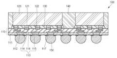
도 1을 참조하면, 본 발명의 일 실시예에 따른 반도체 디바이스(100)의 단면도가 도시되어 있다.Referring to Figure 1, a cross-sectional view of a
도 1에 도시된 바와 같이, 본 발명에 따른 반도체 디바이스(100)는 인터포저(110), 반도체 다이(120), 언더필(130), 인캡슐란트(140) 및 도전성 범프(150)를 포함한다.1, a
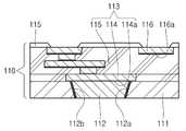
인터포저(110)는 도전성 비아(112)를 갖는 스티프너(111), 재배선(114)을 포함하는 재배선층(113) 및 언더 범프 메탈(117)을 포함한다. 이러한 인터포저(110)는 반도체 다이(120)와 회로기판(또는 외부 장치) 사이에서, 이들 사이의 전기적 신호를 중개하는 역할을 한다.The
스티프너(111)는 대체로 평평한 상면과, 이의 반대면으로서 대략 평평한 하면을 포함하며, 이는 실리콘, 글래스, 세라믹 및 이의 등가물 중에서 선택된 어느 하나로 형성될 수 있다. 그러나, 본 발명에서 이러한 스티프너(111)의 재질이 한정되지 않는다. 스티프너(111)는 전반적으로 인터포저(110)의 기계적 스티프니스(mechanical stiffness)를 향상시킴으로써, 반도체 디바이스(100)의 신뢰성을 향상시키는 역할을 한다. 도전성 비아(112)는 스티프너(111)에 형성되며, 이는 스티프너(111)의 상면에 형성된 재배선(114)과, 스티프너(111)의 하면에 형성된 언더 범프 메탈(117)을 전기적으로 상호간 연결하는 역할을 한다. 이러한 도전성 비아(112)는 대체로 구리, 알루미늄, 금, 은, 그 합금 및 그 등가물 중에서 선택된 어느 하나로 형성될 수 있으나, 이로서 본 발명이 한정되지 않는다.The
재배선층(113)은 대체로 스티프너(111)의 상면에 형성되며, 이는 재배선(114), 유전층(115) 및 마이크로 범프 패드(116)를 포함한다. 재배선(114)은 도전성 비아(112)에 전기적으로 연결되며, 이는 필요에 따라 다층으로 형성될 수 있다. 더불어, 유전층(115)은 스티프너(111) 및 재배선(114)을 덮으며, 이 역시 필요에 따라 다층으로 형성될 수 있다. 마이크로 범프 패드(116)는 최상위의 재배선(114)에 연결되며, 이는 반도체 다이(120)에 전기적으로 연결될 수 있도록 유전층(115)으로 덮이지 않는다. 여기서, 재배선(114) 및 마이크로 범프 패드(116)는 구리, 알루미늄, 금, 은, 그 합금 및 그 등가물 중에서 선택된 어느 하나로 형성될 수 있으나, 이로서 본 발명이 한정되지 않는다. 또한, 유전층(115)은 실리콘 산화막, 실리콘 질화막, 폴리이미드(polyimide), 벤조사이클로부틴(Benzo Cyclo Butene), 폴리벤즈옥사졸(Poly Benz Oxazole) 및 그 등가물 중에서 선택된 어느 하나로 형성될 수 있으나, 이로서 본 발명이 한정되지 않는다.The
언더 범프 메탈(117)은 스티프너(111)의 하면에 형성되며, 이는 도전성 비아(112)에 연결된다. 언더 범프 메탈(117)은 크롬, 니켈, 팔라듐, 금, 은, 그 합금 및 그 등가물 중에서 선택된 적어도 하나 이상으로 형성될 수 있으나, 이로서 본 발명이 한정되지 않는다. 이러한 언더 범프 메탈(117)은 도전성 비아(112)와 도전성 범프(150) 사이의 직접적인 금속간 화합물이 형성되지 않도록 함으로써, 도전성 범프(150)의 신뢰성이 향상되도록 한다.An under
반도체 다이(120)는 재배선층(113)에 전기적으로 접속된다. 이를 위해 반도체 다이(120)는 카파 필라(Cu pillar) 또는 카파 포스트(Cu post)와 같은 마이크로 범프(121)를 포함하며, 이는 솔더(122)를 통해서 재배선층(113)에 구비된 마이크로 범프 패드(116)에 전기적으로 연결될 수 있다. 이러한 반도체 다이(120)는, 예를 들면, 디지털 시그널 프로세서(DSP), 마이크로프로세서, 네트워크 프로세서, 파워 매니지먼트 프로세서, 오디오 프로세서, RF 회로, 와이어리스 베이스 밴드 시스템-온-칩(SoC) 프로세서, 센서 및 주문형 집적회로와 같은 전기적 회로를 포함할 수 있다.The semiconductor die 120 is electrically connected to the
언더필(130)은 반도체 다이(120)와 인터포저(110) 사이에 개재되며, 이는 반도체 다이(120)가 인터포저(110)에 더욱 강건하게 기계적으로 접속되도록 한다. 물론, 이러한 언더필(130)은 마이크로 범프(121) 및 솔더(122)를 감싼다. 특히, 언더필(130)은 반도체 다이(120)와 인터포저(110) 사이의 열팽창 계수차에 의해, 반도체 다이(120)와 인터포저(110)가 전기적으로 분리되는 디라미네이션(delamination) 현상을 예방한다. 또한, 언더필(130)은 경우에 따라 생략될 수도 있다.The
인캡슐란트(140)는 인터포저(110)의 상면에 위치된 반도체 다이(120)를 인캡슐레이션한다. 즉, 인캡슐란트(140)는 언더필(130) 및 반도체 다이(120)를 감쌈으로써, 이들을 외부 환경으로부터 안전하게 보호한다. 경우에 따라, 인캡슐란트(140)는 반도체 다이(120)의 상면을 덮지 않고, 반도체 다이(120)의 상면이 직접 외부로 노출되도록 하여, 반도체 다이(120)의 열방출 효율이 향상되도록 한다.The
한편, 인캡슐란트(140)를 이루는 무기물 필러(filler)의 직경이 반도체 다이(120)와 인터포저(110) 사이의 갭 사이즈(gap size)보다 작은 경우, 상술한 언더필(130)은 사용되지 않을 수도 있다. 예를 들면, 필러 사이즈가 상술한 갭 사이즈보다 작은 몰디드 언더필(Molded Underfill: MUF)이 이용되면, 2단계의 공정(언더필링+인캡슐레이션)이 1단계(인캡슐레이션)의 공정으로 단축될 수 있다.When the diameter of the inorganic filler constituting the
도전성 범프(150)는 인터포저(110)의 하면에 형성된 언더 범프 메탈(117)에 접속되거나 도전성 비아에 접속된다. 이러한 도전성 범프(150)는 공융점 솔더(eutectic solder: Sn37Pb), 고융점 솔더(High lead solder: Sn95Pb), 납이 없는 솔더(lead-free solder: SnAg, SnAu, SnCu, SnZn, SnZnBi, SnAgCu, SnAgBi 등) 중 선택된 하나로 형성될 수 있으며, 여기서 그 재질이 한정되지 않는다.The
이와 같이 하여 본 발명에 따른 반도체 디바이스(100)는 스티프너(111) 위에 재배선층(113)이 형성된 인터포저(110)를 제공함으로써, 인터포저(110)의 기계적 스티프니스(mechanical stiffness)가 향상되어 신뢰성이 향상된다. 즉, 본 발명에 따른 반도체 디바이스(100)는 경도 및/또는 강도가 높은 실리콘, 글래스 또는 세라믹과 같은 스티프너(111) 위에 재배선층(113)이 형성된 인터포저(110)가 제공됨으로써, 기존에 비해 인터포저(110)의 기계적 스티프니스가 향상되고, 이에 따라 반도체 디바이스(100)의 제조 공정 중 인터포저(110)의 취급이 용이해지고, 또한 완성된 반도체 디바이스(100)의 기계적 신뢰성이 향상되도록 한다. 특히, 본 발명에 따른 반도체 디바이스(100)는 인터포저(110)의 기계적 스티프니스 향상에 따라, 언더 범프 메탈(117)과 도전성 범프(150) 사이의 계면 박리 현상도 효과적으로 억제되도록 한다.As described above, the
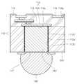
도 2a를 참조하면, 다마신 공정에 의해 스티프너(111)에 형성된 도전성 비아(112)의 단면도가 도시되어 있고, 도 2b를 참조하면, 플라즈마 식각 공정에 의해 실리콘 기판(111')에 형성된 관통 전극(112')의 확대 단면도가 도시되어 있다.Referring to FIG. 2A, a cross-sectional view of a conductive via 112 formed on a
도 2a에 도시된 바와 같이, 다마신 공정에 의해 스티프너(111)의 상면과 하면을 관통하는 도전성 비아(112)가 형성되며, 이의 단면 형태는 대략 역사다리꼴이다. 실질적으로, 도전성 비아(112)의 상면 직경이 하면 직경보다 약간 크다. 또한, 도전성 비아(112)의 대향되는 양측면은 실질적으로 평평한 경사면 형태이다.As shown in FIG. 2A, a conductive via 112 is formed through the upper surface and the lower surface of the
그러나, 도 2b에 도시된 바와 같이, 플라즈마 식각 공정에 의해 실리콘 기판(111')에 형성된 관통 전극(112')은 단면 형태가 대략 사각형이다. 즉, 관통 전극(112')의 상면 직경과 하면 직경이 대략 동일하다. 더욱이, 관통 전극(112')의 양측면에는 공정상의 특성으로 인해 다수의 스칼롭(scallop) 또는 엠보싱(112c')이 형성된다. 즉, 관통 전극(112')의 양측면이 평평한 면이 아니고, 다수의 스칼롭 또는 엠보싱(112c')을 갖는 거친 면이다.However, as shown in FIG. 2B, the penetrating electrode 112 'formed on the silicon substrate 111' by the plasma etching process has a substantially rectangular cross-sectional shape. That is, the diameter of the upper surface of the through electrode 112 'is substantially equal to the lower diameter. Moreover, on both sides of the penetrating electrode 112 ', a number of scallops or
또한, 다마신 공정에 의해 스티프너(111)에 형성된 도전성 비아(112)의 종횡비는 대략 1:1 내지 1:2인 반면, 플라즈마 식각 공정에 의해 실리콘 기판(111')에 형성된 관통 전극(112')의 종횡비는 대략 1:10 내지 1:15이다. 따라서, 본 발명에 따른 도전성 비아(112)의 전기적 경로가 통상의 관통 전극(112')의 전기적 경로보다 훨씬 짧다. 또한, 다마신 공정에 의해 스티프너(111)에 형성된 도전성 비아(112)의 직경은 대략 10 ㎛ 내지 20 ㎛일 수 있으나, 플라즈마 식각 공정에 의해 실리콘 기판(111')에 형성된 관통 전극(112')의 직경은 20 ㎛보다 훨씬 크다.In addition, the aspect ratio of the
더불어, 스티프너(111)와 도전성 비아(112) 사이에는 절연층(112a) 및 시드층(112b)이 더 개재될 수 있다. 절연층(112a)은 스티프너(111)가 실리콘일 경우 실리콘 산화막 또는 실리콘 질화막과 같은 무기막일 수 있으나, 이로서 본 발명이 한정되지 않는다. 더욱이, 절연층(112a)은 스티프너(111)가 글래스 또는 세라믹일 경우 폴리이미드, 벤조사이클로부틴, 폴리벤즈옥사졸과 같은 유기막일 수 있으나, 이로서 본 발명이 한정되지 않는다. 또한, 시드층(112b)은 통상의 티타늄/카파, 티타늄텅스텐/카파, 그 합금 및 그 등가물 중에서 선택된 어느 하나일 수 있으나, 이로서 본 발명이 한정되지 않는다.In addition, an insulating
한편, 실리콘 기판(111')과 관통 전극(112') 사이에도 절연층(112a') 및 시드층(112b')이 더 개재될 수 있는데, 이 경우 공정상의 특성으로 인하여 절연층(112a') 및 시드층(112b)에도 여전히 다수의 스칼롭 또는 엠보싱(112c')이 잔존하게 된다.In addition, the insulating
즉, 본 발명에서는 공정상의 특성으로 인하여 도전성 비아(112)에 스칼롭 또는 엠보싱이 없는 반면, 통상의 기술에서는 공정상의 특성으로 인해 관통 전극(112')에 스칼롭 또는 엠보싱이 잔존한다.That is, in the present invention, the
도 3을 참조하면, 본 발명의 다른 실시예에 따른 반도체 디바이스(200)의 단면도가 도시되어 있다.3, a cross-sectional view of a
도 3에 도시된 바와 같이, 본 발명에 따른 반도체 디바이스(200)는 회로기판(210), 리드(lid)(220) 및 도전성 볼(230)을 더 포함할 수 있다.3, the
즉, 상술한 반도체 디바이스(100)가 도전성 범프(150)를 통하여 회로기판(210)에 전기적으로 접속된다. 회로기판(210)에는 필요에 따라 다양한 수동소자(211)가 더 실장될 수 있다. 더욱이, 반도체 디바이스(100)와 회로기판(210) 사이에는 필요에 따라 언더필(212)이 개재될 수 있다. 또한, 리드(220)는 상술한 회로기판(210) 위의 반도체 디바이스(100) 및 수동소자(211)를 덮음으로써, 반도체 디바이스(100) 및 수동소자(211)가 외부 환경으로부터 보호되도록 한다. 더불어, 도전성 볼(230)은 회로기판(210)에 전기적으로 접속되며, 이는 외부 장치(메인보드 또는 마더보드)에 실장되는 역할을 한다. 여기서, 리드(220)는 접착제(221)에 의해 회로기판(210)에 접착될 수 있고, 또한 접착제(222)에 의해 반도체 디바이스(100)에 접착될 수 있다.That is, the above-described
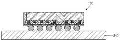
도 4를 참조하면, 본 발명의 또 다른 실시예에 따른 반도체 디바이스(100)의 단면도가 도시되어 있다.Referring to Figure 4, a cross-sectional view of a
도 4에 도시된 바와 같이, 본 발명에 따른 반도체 디바이스(100)는 상술한 바와 같은 회로기판이 아니라 메인보드 또는 마더보드와 같은 외부 장치(240)에 직접 실장될 수도 있다.4, the
도 5a 내지 도 5k을 참조하면, 본 발명의 또 다른 실시예에 따른 반도체 디바이스(100)의 제조 방법에 대한 순차 단면도가 도시되어 있다.5A through 5K, there is shown a sequential cross-sectional view of a method of fabricating a
도 5a에 도시된 바와 같이, 스티프너(111)에 일정 깊이의 트렌치(111a)가 형성된다. 이러한 트렌치(111a)는 통상의 저가형 식각 공정에 의해 형성되므로, 트렌치(111a)의 단면 형태는 대략 역사다리꼴 형태로 형성된다. 즉, 트렌치(111a)의 단면 형태는 바닥면(111b)과 양측면(111c)을 포함하는데, 바닥면(111b)은 대략 수평 방향으로 평평하고, 양측면(111c)은 대략 수직 방향으로 평평하게 경사져 있다. 다르게 설명하면, 트렌치(111a)는 깊이가 깊어짐에 따라 직경이 작아지게 형성되어 있다. 이러한 트렌치(111a)의 단면 형태는 식각 공정 중 발생하는 이방성 식각 특성 때문이다.As shown in FIG. 5A, a
도 5b에 도시된 바와 같이, 트렌치(111a) 및 그 외측 영역에 순차적으로 절연층(112a) 및 시드층(112b)이 형성된다. 여기서, 절연층(112a)은 스티프너(111)가 실리콘일 경우 실리콘 산화막 또는 실리콘 질화막과 같은 무기막일 수 있고, 스티프너(111)가 글래스 또는 세라믹일 경우 폴리이미드, 벤조사이클로부틴, 폴리벤즈옥사졸과 같은 유기막일 수 있다.As shown in FIG. 5B, an insulating
일례로, 실리콘 산화막 또는 실리콘 질화막과 같은 무기막은 대략 900 ℃ 이상의 분위기에서 실리콘에 산소 가스 및/또는 질소 가스가 공급됨으로써, 일정 두께의 실리콘 산화막 및/또는 실리콘 질화막이 형성될 수 있으나, 이로서 본 발명이 한정되지 않는다.For example, an inorganic film such as a silicon oxide film or a silicon nitride film may be formed with a silicon oxide film and / or a silicon nitride film of a certain thickness by supplying oxygen gas and / or nitrogen gas to silicon in an atmosphere of about 900 ° C or higher. Is not limited.
다른예로, 폴리이미드와 같은 유기막은 스핀 코팅(spin coating), 스프레이 코팅(spray coating), 딥 코팅(dip coating) 또는 로드 코팅(rod coating)에 의해 형성될 수 있으나, 이로서 본 발명이 한정되지 않는다.As another example, an organic film such as polyimide may be formed by spin coating, spray coating, dip coating or rod coating, but the present invention is not limited thereto Do not.
한편, 시드층(112b)은 티타늄/카파, 티타늄텅스텐/카파로 형성될 수 있다. 일례로, 시드층(112b)은 무전해 도금, 전해 도금 및/또는 스퍼터링 공정에 의해 형성될 수 있으나, 이로서 본 발명이 한정되지 않는다.On the other hand, the
도 5c에 도시된 바와 같이, 절연층(112a) 및 시드층(112b)이 형성된 트렌치(111a) 및 그 외측 영역에 일정 두께의 도전층(1120)이 형성될 수 있다. 이러한 도전층(1120)은 구리, 알루미늄, 금, 또는 은일 수 있으나, 이러한 재질로 본 발명이 한정되지 않는다. 한편, 이러한 도전층(1120)은, 일례로, 무전해 도금, 전해 도금 및/또는 스퍼터링 공정에 의해 형성될 수 있으나, 이로서 본 발명이 한정되지 않는다.A
도 5d에 도시된 바와 같이, 트렌치(111a) 및 그 외측에 일정 두께로 형성된 도전층(1120)은 평탄화 공정 또는 CMP(Chemical Mehanical polishing) 공정에 의해 일정 부분 제거된다. 일례로, 스티프너(111)의 상측으로서 트렌치(111a) 외측의 도전층(1120)이 모두 제거됨으로써, 도전층(1120)은 트렌치(111a)의 내부에만 잔존하게 된다. 이하에서는 이러한 도전층(1120)을 도전성 비아(112)로 칭하기로 한다.As shown in FIG. 5D, the
도 5e에 도시된 바와 같이, 스티프너(111) 위에 적어도 1층의 재배선(114) 및 유전층(115)이 형성되고, 또한 최상위 재배선(114)에 마이크로 범프 패드(116)가 형성됨으로써, 재배선층(113)이 완성된다. 즉, 스티프너(111)의 도전성 비아(112)에 연결되도록 재배선 시드층(114a)이 형성되고, 재배선 시드층(114a) 위에 재배선(114)이 형성되며, 재배선(114)은 유전층(115)으로 마감된다. 또한, 최상위 재배선(114)에 패드 시드층(116a)이 형성되고, 패드 시드층(116a) 위에 마이크로 범프 패드(116)가 형성된다. 여기서, 마이크로 범프 패드(116)는 추후 반도체 다이(120)와 전기적으로 연결될 수 있도록 유전층(115)으로 덮이지 않고 외측으로 노출된다.5E, at least one layer of the redistribution traces 114 and the
여기서, 재배선 시드층(114a) 및 패드 시드층(116a)은 티타늄/카파, 티타늄텅스텐/카파가 통상의 무전해 도금, 전해 도금 또는 스퍼터링 공정에 의해 형성될 수 있다. 또한, 재배선층(113) 및 마이크로 범프 패드(116)는 구리, 알루미늄, 금 또는 은이 무전해 도금, 전해 도금 또는 스퍼터링 공정 및/또는 사진 식각 공정에 의해 형성될 수 있다. 더불어, 유전층(115)은 폴리이미드, 벤조사이클로부틴 또는 폴리벤즈옥사졸이 스핀 코팅, 스프레이 코팅, 딥 코팅 또는 로드 코팅에 의해 형성될 수 있다.Here, the
도 5f에 도시된 바와 같이, 스티프너(111) 중 트렌치(111a)의 하부 영역이 평탄화 공정 또는 CMP 공정에 의해 제거된다. 따라서, 트렌치(111a)에 형성된 도전성 비아(112)의 하면이 외부로 노출되며, 이때 도전성 비아(112)의 하면에 형성된 절연층(112a) 및 시드층(112b)도 함께 제거될 수 있다. 즉, 평탄화 공정 및 CMP 공정에 의해 도전성 비아(112), 예를 들면, 카파의 하면이 직접 하부로 노출될 수 있으며, 이때 당연히 스티프너(111)의 하면과 도전성 비아(112)의 하면은 동일한 평면을 이룬다.The lower region of the
도 5g에 도시된 바와 같이, 스티프너(111)의 하면을 통해 노출된 도전성 비아(112)에 언더 범프 메탈(117)이 형성된다. 즉, 도전성 비아(112)의 하면에 메탈 시드층(117a)이 형성되고, 그 메탈 시드층(117a)에 언더 범프 메탈(117)이 형성된다. 메탈 시드층(117a)은 티타늄/카파, 티타늄텅스텐/카파가 통상의 무전해 도금, 전해 도금 또는 스퍼터링 공정에 의해 형성될 수 있다. 또한, 언더 범프 메탈(117)은 크롬, 니켈, 팔라듐, 금, 은, 이들의 합금 및 그 등가물 중에서 선택된 적어도 하나 이상으로 형성될 수 있으나, 이로서 본 발명이 한정되지 않는다. 더불어, 언더 범프 메탈(117) 역시 통상의 무전해 도금, 전해 도금 및/또는 스퍼터링 공정에 의해 형성될 수 있다. 이러한 언더 범프 메탈(117)은 하기할 도전성 범프(150)와 도전성 비아(112) 사이의 직접적인 금속간 화합물이 형성되지 않도록 함으로써, 도전성 범프(150)의 보드 레벨 신뢰성이 향상되도록 한다. 더불어, 필요에 따라 언더 범프 메탈(117)과 스티프너(111)의 사이에는 유전층(115)이 더 형성될 수도 있다. 또한, 경우에 따라 언더 범프 메탈(117)은 생략될 수 있다.The
이와 같이 하여 도전성 비아(112)를 갖는 스티프너(111)와, 재배선(114), 유전층(115), 마이크로 범프 패드(116) 및 언더 범프 메탈(117)을 갖는 재배선층(113)을 포함하는 인터포저(110)가 완성된다.In this manner, the
도 5h에 도시된 바와 같이, 인터포저(110)에 적어도 하나의 반도체 다이(120)가 전기적으로 접속된다. 일례로, 반도체 다이(120)는 마이크로 범프(121) 및 솔더(122)를 통해 인터포저(110)의 마이크로 범프 패드(116)에 전기적으로 접속될 수 있다. 일례로, 인터포저(110)의 마이크로 범프 패드(116)에 휘발성 플럭스가 돗팅되고, 그 위에 마이크로 범프(121)를 갖는 반도체 다이(120)가 정렬된다. 이후, 대략 150 ℃ 내지 250 ℃의 온도가 제공되면, 상술한 마이크로 범프(121)이 하단에 형성된 솔더(122)가 용융되면서 마이크로 범프 패드(116)에 융착된다. 이어서, 냉각 공정을 통과하게 되면 마이크로 범프(121)의 하단에 형성된 솔더(122)가 경화됨으로써, 반도체 다이(120)가 인터포저(110)에 완전하게 전기적 및 기계적으로 접속된다. 이외에도 반도체 다이를 인터포저에 접속 방법은 다양하게 적용 가능하다.At least one semiconductor die 120 is electrically connected to the
도 5i에 도시된 바와 같이, 반도체 다이(120)와 인터포저(110)의 사이의 갭 또는 공간에 언더필(130)이 충진된다. 예를 들면, 디스펜서에 수용된 언더필(130)이 반도체 다이(120)와 인터포저(110) 사이의 갭에 디스펜싱된 후 경화됨으로써, 언더필(130)에 의해 반도체다이(120)와 인터포저(110)가 상호간 기계적으로 결합된다.The gap or space between the semiconductor die 120 and the
경우에 따라 언더필 충진 공정은 생략될 수 있다.In some cases, the underfill filling process may be omitted.
도 5j에 도시된 바와 같이, 인터포저(110) 상면의 반도체 다이(120) 및 언더필(130)이 인캡슐란트(140)에 의해 인캡슐레이션된다. 이때, 반도체 다이(120)의 상면은 인캡슐란트(140)를 통해 외측으로 노출될 수 있다.The semiconductor die 120 and the
도 5k에 도시된 바와 같이, 인터포저(110) 하면의 언더 범프 메탈(117)에 도전성 범프(150)이 접속된다. 일례로, 언더 범프 메탈(117)에 휘발성 플럭스가 돗팅되고, 그 위에 도전성 범프(150)가 임시로 위치된다. 이후, 대략 150 ℃ 내지 250 ℃의 온도가 제공되면, 상술한 도전성 범프(150)가 용융되면서 언더 범프 메탈(117)에 융착된다. 이어서, 냉각 공정을 통과하게 되면 도전성 범프(150)가 경화됨으로써, 도전성 범프(150)가 인터포저(110)에 완전하게 전기적으로 접속된다.The
물론, 이러한 접속 방법은 다른 방식으로 구현될 수도 있다.Of course, this connection method may be implemented in other ways.
더불어, 이러한 공정은 유닛, 패널, 스트립, 웨이퍼 또는 매트릭스 단위로 수행될 수 있는데, 패널, 스트립, 웨이퍼 또는 매트릭스 단위로 수행되었을 경우, 소잉 공정 등이 뒤따를 수 있다. 즉, 패널, 스트립, 웨이퍼 또는 매트릭스로부터 낱개의 반도체 디바이스(100)가 소잉 또는 펀칭 공정에 의해 독립된다.In addition, such a process can be performed in units of units, panels, strips, wafers, or matrices, such as sowing processes, if performed in a panel, strip, wafer, or matrix unit. That is, the
이와 같이 하여, 본 발명에 따르면, 인터포저(110)에 고가의 플라즈마 식각 공정 또는 레이저 드릴링 공정에 의한 관통 전극이 아닌 저가의 다마신 공정에 의한 도전성 비아(112)가 형성됨으로써, 인터포저(110)의 제조 비용이 낮은 반도체 디바이스(100)가 제공된다. 즉, 스티프너(111)에 트렌치(111a)가 형성되고, 그 트렌치(111a)에 도전층(1120)이 형성된 이후, 스티프너(111)의 일부 영역이 평탄화 공정 또는 그라인딩 공정에 의해 제거됨으로써, 상면과 하면이 전기적으로 연결된 도전성 비아(112)가 완성된다. 따라서, 본 발명에서는 고가의 플라즈마 식각 공정 또는 레이저 드릴링 공정의 도움없이도, 기존의 관통 전극과 동일한 기능을 하는 도전성 비아(112)가 저렴하게 형성될 수 있다.As described above, according to the present invention, since the
도 6a 내지 도 6g를 참조하면, 본 발명의 또 다른 실시예에 따른 반도체 디바이스의 제조 방법에 대한 순차 단면도가 도시되어 있다. 여기서, 재배선층 위에 형성되는 반도체 다이, 언더필 및 인캡슐란트의 구성은 위에서 설명한 것과 동일하므로, 이 부분에 대한 설명은 생략한다.6A to 6G, a sequential sectional view of a method of manufacturing a semiconductor device according to another embodiment of the present invention is shown. Here, the structures of the semiconductor die, the underfill and the encapsulant formed on the re-wiring layer are the same as those described above, and therefore, a description thereof will be omitted.
도 6a에 도시된 바와 같이, 스티프너(311)에 일정 깊이의 2중 트렌치(311a)가 형성된다. 즉, 스티프너(311)에 상대적으로 깊고 상대적으로 좁은 제1트렌치(311b)가 형성되고, 그 위에 상대적으로 얕고 상대적으로 넓은 제2트렌치(311c)가 형성된다. 이러한 2중 트렌치(311a)는 통상의 사진 식각 공정에 의해 형성되므로, 2중 트렌치(311a)의 단면 형태는 대략 2개의 역사다리꼴 형태로 형성된다.As shown in Fig. 6A, a
도 6b에 도시된 바와 같이, 2중 트렌치(311a) 및 그 외측 영역에 순차적으로 절연층(312a) 및 시드층(312b)이 형성된다. 여기서, 절연층(312a)은 스티프너(311)가 실리콘일 경우 실리콘 산화막 또는 실리콘 질화막과 같은 무기막일 수 있고, 스티프너(311)가 글래스 또는 세라믹일 경우 폴리이미드, 벤조사이클로부틴, 폴리벤즈옥사졸과 같은 유기막일 수 있다.As shown in FIG. 6B, an insulating
도 6c에 도시된 바와 같이, 절연층(312a) 및 시드층(312b)이 형성된 2중 트렌치(311a) 및 그 외측 영역에 일정 두께의 도전층(3120)이 형성될 수 있다.A
도 6d에 도시된 바와 같이, 2중 트렌치(311a) 및 그 외측에 일정 두께로 형성된 도전층(3120)은 평탄화 공정 또는 CMP(Chemical Mehanical polishing) 공정에 의해 일정 부분 제거된다. 일례로, 스티프너(311)의 상면으로서 트렌치(311a) 외측의 도전층(3120)이 모두 제거됨으로써, 도전층(3120)은 2중 트렌치(311a)의 내부에만 잔존하게 된다. 여기서, 제1트렌치(311b)에 충진된 도전층(3120)은 추후 도전성 필라(317)가 되고, 제2트렌치(311c)에 충진된 도전층(3120)은 추후 도전성 비아(312)가 된다. 이하에서는, 이와 같이 도전성 필라(317) 및 도전성 비아(312)로 부른다.As shown in FIG. 6D, the
도 6e에 도시된 바와 같이, 스티프너(311) 위에 적어도 1층의 재배선(314) 및 유전층(315)이 형성되고, 또한 최상위 재배선(314)에 마이크로 범프 패드(316)가 형성됨으로써, 재배선층(313)이 완성된다. 즉, 스티프너(311)의 도전성 비아(312)에 연결되도록 재배선 시드층(314a)이 형성되고, 재배선 시드층(314a) 위에 재배선(314)이 형성되며, 재배선(314)은 유전층(315)으로 덮인다. 또한, 최상위 재배선(314)에 패드 시드층(316a)이 형성되고, 패드 시드층(316a) 위에 마이크로 범프 패드(316)가 형성된다.At least one layer of the
도 6f에 도시된 바와 같이, 스티프너(311) 중 제1트렌치(311b)의 하부 영역이 평탄화 공정 또는 CMP 공정에 의해 제거된다. 또한, 스티프너(311) 중 제1트렌치(311b)의 외측 즉, 도전성 필라(317)의 외측 영역이 식각되어 제거됨으로써, 마치 도전성 비아(312)로부터 도전성 필라(317)가 하부 방향으로 일정 길이 연장된 형태가 얻어진다. 또한, 도전성 비아(312)는 스티프너(311) 내부에 위치된 형태를 하고, 도전성 필라(317)는 스티프너(311)의 하부로 일정 길이 연장된 형태를 한다.The lower region of the
여기서, 도전성 필라(317)의 하면에 위치된 절연층(312a)은 제거됨으로써, 도전성 필라(317)의 하면에 솔더(318)가 전기적으로 접속되도록 한다. 도전성 필라(317)의 하면에 위치된 시드층(312b)은 잔존할 수도 있고, 필요에 따라 제거할 수도 있다.Here, the insulating
또한, 상술한 솔더(318)는 인터포저(310) 위에 반도체 다이가 부착되고, 언더필 및 인캡슐란트가 적용된 이후 형성될 수도 있다. 더불어, 반도체 다이, 언더필 및 인캡슐란트의 구조는 이미 위에서 설명한 것과 동일하므로 이에 대한 제조 방법 및 구성의 설명은 생략한다.The
이와 같이 하여, 본 발명은 인터포저(310)에 다마신 공정에 의해 도전성 필라(317)가 함께 형성됨으로써, 파인 피치의 도전성 필라(317)가 구현될 수 있다. 즉, 스티프너(311)에 2중 트렌치(311a)가 형성되고, 2중 트렌치(311a)에 도전층(3120)이 충진된 이후, 스티프너(311)의 일부 영역이 평탄화 공정 또는 그라인딩 공정과, 식각 공정에 의해 제거됨으로써, 상면과 하면을 전기적으로 연결하는 도전성 비아(312) 및 도전성 비아(312)에 일체로 형성된 도전성 필라(317)가 구현된다. 따라서, 본 발명에서는 파인 피치를 갖는 도전성 필라(317)가 저렴하게 형성될 수 있다.In this manner, the
이상에서 설명한 것은 본 발명에 따른 반도체 디바이스를 실시하기 위한 하나의 실시예에 불과한 것으로서, 본 발명은 상기한 실시예에 한정되지 않고, 이하의 특허청구범위에서 청구하는 바와 같이 본 발명의 요지를 벗어남이 없이 당해 발명이 속하는 분야에서 통상의 지식을 가진 자라면 누구든지 다양한 변경 실시가 가능한 범위까지 본 발명의 기술적 정신이 있다고 할 것이다.It is to be understood that the present invention is not limited to the above-described embodiment, but may be modified in various ways within the spirit and scope of the present invention as set forth in the following claims It will be understood by those of ordinary skill in the art that various changes in form and details may be made therein without departing from the spirit and scope of the invention.
100; 본 발명에 따른 반도체 디바이스
110; 인터포저111; 스티프너
111a; 트렌치111b; 바닥면
111c; 양측면1120; 도전층
112; 도전성 비아112a; 절연층
112b; 시드층113; 재배선층
114; 재배선114a; 재배선 시드층
115; 유전층116; 마이크로 범프 패드
116a; 패드 시드층117; 언더 범프 메탈
117a; 메탈 시드층120; 반도체 다이
121; 마이크로 범프122; 솔더
130; 언더필140; 인캡슐란트
150; 도전성 범프
200; 본 발명에 따른 반도체 디바이스
210; 회로기판211; 수동소자
212; 언더필220; 리드
221, 222; 접착제230; 도전성 볼
240; 외부 장치
310; 인터포저311; 스티프너
311a; 트렌치311b; 제1트렌치
311c; 제2트렌치3120; 도전층
312; 도전성 비아312a; 절연층
312b; 시드층313; 재배선층
314; 재배선314a; 재배선 시드층
315; 유전층316; 마이크로 범프 패드
316a; 패드 시드층317; 도전성 필라
318; 솔더100; The semiconductor device
110;
111a;
111c; Both
112; Conductive vias 112a; Insulating layer
112b;
114;
115; A
116a;
117a; A
121; Micro bumps 122; Solder
130;
150; Conductive bump
200; The semiconductor device
210; A
212;
221, 222; Adhesive 230; Conductive ball
240; External device
310;
311a;
311c; A
312; Conductive vias 312a; Insulating layer
312b; A
314;
315; A
316a;
318; Solder
Claims (18)
Translated fromKorean상기 인터포저의 재배선층에 접속된 반도체 다이를 포함하고,
상기 도전성 비아로부터 연장되되, 상기 스티프너의 외측으로 돌출된 도전성 필라를 더 포함하고,
상기 도전성 비아와 상기 도전성 필라는 일체로 형성되며,
상기 도전성 비아와 상기 도전성 필라의 표면에 시드층이 형성되고, 상기 시드층의 표면에 절연층이 형성되며,
상기 절연층은 상기 스티프너의 외측으로 돌출된 것을 특징으로 하는 반도체 디바이스.An interposer comprising a stiffener having a conductive via and a re-wiring layer connected to the conductive via; And
And a semiconductor die connected to the re-wiring layer of the interposer,
Further comprising a conductive pillar extending from the conductive via, the conductive pillar protruding outward of the stiffener,
Wherein the conductive via and the conductive pillar are integrally formed,
A seed layer is formed on the surface of the conductive via and the conductive pillar, an insulating layer is formed on a surface of the seed layer,
Wherein the insulating layer protrudes outside the stiffener.
상기 스티프너는 실리콘, 글래스 또는 세라믹인 것을 특징으로 하는 반도체 디바이스.The method according to claim 1,
Wherein the stiffener is silicon, glass or ceramic.
상기 도전성 비아는 종횡비가 1:1 내지 1:2인 것을 특징으로 하는 반도체 디바이스.The method according to claim 1,
Wherein the conductive vias have an aspect ratio of 1: 1 to 1: 2.
상기 도전성 비아는 단면 형태가 역사다리꼴인 것을 특징으로 하는 반도체 디바이스.The method according to claim 1,
Wherein the conductive vias have an inverted trapezoidal cross-sectional shape.
상기 도전성 비아는 상면의 직경이 하면의 직경보다 큰 것을 특징으로 하는 반도체 디바이스.The method according to claim 1,
Wherein the conductive via is larger in diameter on the upper surface than on the lower surface.
상기 도전성 비아는 직경이 10 ㎛ 내지 20 ㎛인 것을 특징으로 하는 반도체 디바이스.The method according to claim 1,
Wherein the conductive vias have a diameter of from 10 占 퐉 to 20 占 퐉.
상기 도전성 필라의 직경이 상기 도전성 비아의 직경보다 작은 것을 특징으로 하는 반도체 디바이스.The method according to claim 1,
Wherein the diameter of the conductive pillar is smaller than the diameter of the conductive via.
상기 도전성 필라는 단면 형태가 역사다리꼴인 것을 특징으로 하는 반도체 디바이스.The method according to claim 1,
Wherein the conductive pillar has an inverted trapezoidal cross-sectional shape.
상기 도전성 필라의 하단에 접속된 도전성 범프를 더 포함함을 특징으로 하는 반도체 디바이스.The method according to claim 1,
And a conductive bump connected to a lower end of the conductive pillar.
상기 반도체 다이와 상기 인터포저의 재배선층 사이에 개재된 언더필을 더 포함함을 특징으로 하는 반도체 디바이스.The method according to claim 1,
Further comprising an underfill interposed between the semiconductor die and the re-wiring layer of the interposer.
상기 반도체 다이는 인캡슐란트로 인캡슐레이션된 것을 특징으로 하는 반도체 디바이스.The method according to claim 1,
RTI ID = 0.0 > 1, < / RTI > wherein the semiconductor die is encapsulated in encapsulant.
상기 인터포저의 도전성 비아가 전기적으로 접속된 회로기판;
상기 회로기판 위의 상기 인터포저 및 상기 반도체 다이를 덮는 리드(lid); 및
상기 회로기판의 아래에 접속된 도전성 볼을 더 포함함을 특징으로 하는 반도체 디바이스.The method according to claim 1,
A circuit board on which electrically conductive vias of the interposer are electrically connected;
A lid covering the interposer and the semiconductor die on the circuit board; And
And a conductive ball connected under the circuit board.
Priority Applications (7)
| Application Number | Priority Date | Filing Date | Title |
|---|---|---|---|
| KR1020150089245AKR101672640B1 (en) | 2015-06-23 | 2015-06-23 | Semiconductor device |
| US15/149,158US20160379915A1 (en) | 2015-06-23 | 2016-05-08 | Semiconductor device and manufacturing method thereof |
| TW105117129ATWI796282B (en) | 2015-06-23 | 2016-06-01 | Semiconductor device and manufacturing method thereof |
| TW112106769ATWI896941B (en) | 2015-06-23 | 2016-06-01 | Semiconductor device and manufacturing method thereof |
| CN201610461558.9ACN106298684B (en) | 2015-06-23 | 2016-06-23 | Semiconductor device and method for manufacturing the same |
| CN202210284462.5ACN114823544A (en) | 2015-06-23 | 2016-06-23 | Semiconductor device and method for manufacturing the same |
| CN201620629791.9UCN206040615U (en) | 2015-06-23 | 2016-06-23 | Semiconductor device |
Applications Claiming Priority (1)
| Application Number | Priority Date | Filing Date | Title |
|---|---|---|---|
| KR1020150089245AKR101672640B1 (en) | 2015-06-23 | 2015-06-23 | Semiconductor device |
Publications (1)
| Publication Number | Publication Date |
|---|---|
| KR101672640B1true KR101672640B1 (en) | 2016-11-03 |
Family
ID=57571276
Family Applications (1)
| Application Number | Title | Priority Date | Filing Date |
|---|---|---|---|
| KR1020150089245AActiveKR101672640B1 (en) | 2015-06-23 | 2015-06-23 | Semiconductor device |
Country Status (4)
| Country | Link |
|---|---|
| US (1) | US20160379915A1 (en) |
| KR (1) | KR101672640B1 (en) |
| CN (3) | CN114823544A (en) |
| TW (1) | TWI796282B (en) |
Families Citing this family (16)
| Publication number | Priority date | Publication date | Assignee | Title |
|---|---|---|---|---|
| KR101672640B1 (en)* | 2015-06-23 | 2016-11-03 | 앰코 테크놀로지 코리아 주식회사 | Semiconductor device |
| CN106469692B (en)* | 2015-08-14 | 2021-06-04 | Pep创新私人有限公司 | Semiconductor processing method |
| US9859222B1 (en)* | 2016-06-08 | 2018-01-02 | Samsung Electro-Mechanics Co., Ltd. | Fan-out semiconductor package |
| US9899305B1 (en)* | 2017-04-28 | 2018-02-20 | Taiwan Semiconductor Manufacturing Company Ltd. | Semiconductor package structure |
| DE102018119298B4 (en)* | 2017-09-29 | 2024-05-29 | Taiwan Semiconductor Manufacturing Co., Ltd. | Semiconductor packages |
| KR102081088B1 (en) | 2018-08-29 | 2020-02-25 | 삼성전자주식회사 | Semiconductor package |
| EP3696851B1 (en) | 2019-02-18 | 2022-10-12 | Infineon Technologies AG | Semiconductor arrangement and method for producing the same |
| JP7335036B2 (en)* | 2019-03-29 | 2023-08-29 | ラピスセミコンダクタ株式会社 | Semiconductor package manufacturing method |
| US11735533B2 (en)* | 2019-06-11 | 2023-08-22 | Intel Corporation | Heterogeneous nested interposer package for IC chips |
| KR102615198B1 (en) | 2019-10-15 | 2023-12-18 | 삼성전자주식회사 | Semiconductor package |
| TWI768294B (en)* | 2019-12-31 | 2022-06-21 | 力成科技股份有限公司 | Package structure and manufacturing method thereof |
| KR102866115B1 (en)* | 2020-02-03 | 2025-09-30 | 삼성전자주식회사 | Semiconductor device and a method for manufacturing the same |
| KR102793907B1 (en) | 2020-08-24 | 2025-04-08 | 삼성전자주식회사 | semiconductor package |
| KR20220026308A (en) | 2020-08-25 | 2022-03-04 | 삼성전자주식회사 | Semiconductor package |
| KR20230058949A (en)* | 2021-10-25 | 2023-05-03 | 삼성전자주식회사 | Semiconductor package and method of manufacturing the semiconductor package |
| CN114649292B (en)* | 2022-03-11 | 2025-08-12 | 无锡中微高科电子有限公司 | Three-dimensional fan-out type packaging structure and manufacturing method thereof |
Citations (4)
| Publication number | Priority date | Publication date | Assignee | Title |
|---|---|---|---|---|
| KR20090091484A (en)* | 2008-02-25 | 2009-08-28 | 앰코 테크놀로지 코리아 주식회사 | Semiconductor package |
| US20120074585A1 (en)* | 2010-09-24 | 2012-03-29 | Stats Chippac, Ltd. | Semiconductor Device and Method of Forming TSV Interposer With Semiconductor Die and Build-Up Interconnect Structure on Opposing Surfaces of the Interposer |
| KR20140065724A (en)* | 2012-11-20 | 2014-05-30 | 앰코 테크놀로지 코리아 주식회사 | Semiconductor device using epoxy molding compound wafer support system and fabricating method thereof |
| JP2014517547A (en)* | 2011-06-23 | 2014-07-17 | インターナショナル・ビジネス・マシーンズ・コーポレーション | Integrated circuit structure, integrated circuit, and method of forming a robust TSV structure |
Family Cites Families (58)
| Publication number | Priority date | Publication date | Assignee | Title |
|---|---|---|---|---|
| JPS63245952A (en)* | 1987-04-01 | 1988-10-13 | Hitachi Ltd | Multi-chip module structure |
| JP2716336B2 (en)* | 1993-03-10 | 1998-02-18 | 日本電気株式会社 | Integrated circuit device |
| TW512467B (en)* | 1999-10-12 | 2002-12-01 | North Kk | Wiring circuit substrate and manufacturing method therefor |
| US6586684B2 (en)* | 2001-06-29 | 2003-07-01 | Intel Corporation | Circuit housing clamp and method of manufacture therefor |
| US6780673B2 (en)* | 2002-06-12 | 2004-08-24 | Texas Instruments Incorporated | Method of forming a semiconductor device package using a plate layer surrounding contact pads |
| US7462936B2 (en)* | 2003-10-06 | 2008-12-09 | Tessera, Inc. | Formation of circuitry with modification of feature height |
| US7176043B2 (en)* | 2003-12-30 | 2007-02-13 | Tessera, Inc. | Microelectronic packages and methods therefor |
| JP2006049804A (en)* | 2004-07-07 | 2006-02-16 | Shinko Electric Ind Co Ltd | Manufacturing method of wiring board |
| US7317249B2 (en)* | 2004-12-23 | 2008-01-08 | Tessera, Inc. | Microelectronic package having stacked semiconductor devices and a process for its fabrication |
| US7388296B2 (en)* | 2005-06-09 | 2008-06-17 | Ngk Spark Plug Co., Ltd. | Wiring substrate and bonding pad composition |
| US7667473B1 (en)* | 2005-09-28 | 2010-02-23 | Xilinx, Inc | Flip-chip package having thermal expansion posts |
| US7911805B2 (en)* | 2007-06-29 | 2011-03-22 | Tessera, Inc. | Multilayer wiring element having pin interface |
| US20090071707A1 (en)* | 2007-08-15 | 2009-03-19 | Tessera, Inc. | Multilayer substrate with interconnection vias and method of manufacturing the same |
| US20090148594A1 (en)* | 2007-08-15 | 2009-06-11 | Tessera, Inc. | Interconnection element with plated posts formed on mandrel |
| JP5629580B2 (en)* | 2007-09-28 | 2014-11-19 | テッセラ,インコーポレイテッド | Flip chip interconnect with double posts |
| KR101572600B1 (en)* | 2007-10-10 | 2015-11-27 | 테세라, 인코포레이티드 | Robust multi-layer wiring elements and assemblies with embedded microelectronic elements |
| TWI389290B (en)* | 2007-11-08 | 2013-03-11 | Ind Tech Res Inst | Chip structure and process thereof, stacked structure of chips and process thereof |
| JP2009158593A (en)* | 2007-12-25 | 2009-07-16 | Tessera Interconnect Materials Inc | Bump structure and method of manufacturing the same |
| US20090212420A1 (en)* | 2008-02-22 | 2009-08-27 | Harry Hedler | integrated circuit device and method for fabricating same |
| JP5290017B2 (en)* | 2008-03-28 | 2013-09-18 | 日本特殊陶業株式会社 | Multilayer wiring board and manufacturing method thereof |
| US20100044860A1 (en)* | 2008-08-21 | 2010-02-25 | Tessera Interconnect Materials, Inc. | Microelectronic substrate or element having conductive pads and metal posts joined thereto using bond layer |
| US7915080B2 (en)* | 2008-12-19 | 2011-03-29 | Texas Instruments Incorporated | Bonding IC die to TSV wafers |
| US8115310B2 (en)* | 2009-06-11 | 2012-02-14 | Texas Instruments Incorporated | Copper pillar bonding for fine pitch flip chip devices |
| KR20110000960A (en)* | 2009-06-29 | 2011-01-06 | 삼성전자주식회사 | Semiconductor chip, stack module, memory card and manufacturing method thereof |
| US20110186960A1 (en)* | 2010-02-03 | 2011-08-04 | Albert Wu | Techniques and configurations for recessed semiconductor substrates |
| US20110207323A1 (en)* | 2010-02-25 | 2011-08-25 | Robert Ditizio | Method of forming and patterning conformal insulation layer in vias and etched structures |
| JP5711472B2 (en)* | 2010-06-09 | 2015-04-30 | 新光電気工業株式会社 | WIRING BOARD, MANUFACTURING METHOD THEREOF, AND SEMICONDUCTOR DEVICE |
| US8471577B2 (en)* | 2010-06-11 | 2013-06-25 | Texas Instruments Incorporated | Lateral coupling enabled topside only dual-side testing of TSV die attached to package substrate |
| US8330272B2 (en)* | 2010-07-08 | 2012-12-11 | Tessera, Inc. | Microelectronic packages with dual or multiple-etched flip-chip connectors |
| US8580607B2 (en)* | 2010-07-27 | 2013-11-12 | Tessera, Inc. | Microelectronic packages with nanoparticle joining |
| US8338945B2 (en)* | 2010-10-26 | 2012-12-25 | Taiwan Semiconductor Manufacturing Company, Ltd. | Molded chip interposer structure and methods |
| US8952540B2 (en)* | 2011-06-30 | 2015-02-10 | Intel Corporation | In situ-built pin-grid arrays for coreless substrates, and methods of making same |
| US8501590B2 (en)* | 2011-07-05 | 2013-08-06 | Taiwan Semiconductor Manufacturing Company, Ltd. | Apparatus and methods for dicing interposer assembly |
| US8691691B2 (en)* | 2011-07-29 | 2014-04-08 | International Business Machines Corporation | TSV pillar as an interconnecting structure |
| US9177832B2 (en)* | 2011-09-16 | 2015-11-03 | Stats Chippac, Ltd. | Semiconductor device and method of forming a reconfigured stackable wafer level package with vertical interconnect |
| US8957518B2 (en)* | 2012-01-04 | 2015-02-17 | Mediatek Inc. | Molded interposer package and method for fabricating the same |
| US8770462B2 (en)* | 2012-03-14 | 2014-07-08 | Raytheon Company | Solder paste transfer process |
| US9842798B2 (en)* | 2012-03-23 | 2017-12-12 | STATS ChipPAC Pte. Ltd. | Semiconductor device and method of forming a PoP device with embedded vertical interconnect units |
| US10049964B2 (en)* | 2012-03-23 | 2018-08-14 | STATS ChipPAC Pte. Ltd. | Semiconductor device and method of forming a fan-out PoP device with PWB vertical interconnect units |
| US9030010B2 (en)* | 2012-09-20 | 2015-05-12 | Taiwan Semiconductor Manufacturing Company, Ltd. | Packaging devices and methods |
| KR101411813B1 (en)* | 2012-11-09 | 2014-06-27 | 앰코 테크놀로지 코리아 주식회사 | Semiconductor device and manufacturing method thereof |
| IL223414A (en)* | 2012-12-04 | 2017-07-31 | Elta Systems Ltd | Integrated electronic device and a method for fabricating the same |
| US9070667B2 (en)* | 2013-02-27 | 2015-06-30 | Taiwan Semiconductor Manufacturing Company, Ltd. | Peripheral electrical connection of package on package |
| US9768048B2 (en)* | 2013-03-15 | 2017-09-19 | Taiwan Semiconductor Manufacturing Company, Ltd. | Package on-package structure |
| WO2014193978A1 (en)* | 2013-05-28 | 2014-12-04 | Georgia Tech Research Corporation | Glass-polymer optical interposer |
| US9049791B2 (en)* | 2013-06-07 | 2015-06-02 | Zhuhai Advanced Chip Carriers & Electronic Substrates Solutions Technologies Co. Ltd. | Terminations and couplings between chips and substrates |
| CN103346120A (en)* | 2013-07-01 | 2013-10-09 | 华进半导体封装先导技术研发中心有限公司 | Method for exposing TSV heads in chemical etching mode and corresponding device |
| US9406588B2 (en)* | 2013-11-11 | 2016-08-02 | Taiwan Semiconductor Manufacturing Company Ltd. | Semiconductor package and manufacturing method thereof |
| US9305890B2 (en)* | 2014-01-15 | 2016-04-05 | Taiwan Semiconductor Manufacturing Company, Ltd. | Package having substrate with embedded metal trace overlapped by landing pad |
| US9165793B1 (en)* | 2014-05-02 | 2015-10-20 | Invensas Corporation | Making electrical components in handle wafers of integrated circuit packages |
| US9355983B1 (en)* | 2014-06-27 | 2016-05-31 | Stats Chippac Ltd. | Integrated circuit packaging system with interposer structure and method of manufacture thereof |
| TWI533771B (en)* | 2014-07-17 | 2016-05-11 | 矽品精密工業股份有限公司 | Coreless package substrate and fabrication method thereof |
| US9373564B2 (en)* | 2014-08-07 | 2016-06-21 | Industrial Technology Research Institute | Semiconductor device, manufacturing method and stacking structure thereof |
| US9733304B2 (en)* | 2014-09-24 | 2017-08-15 | Micron Technology, Inc. | Semiconductor device test apparatuses |
| US20160111380A1 (en)* | 2014-10-21 | 2016-04-21 | Georgia Tech Research Corporation | New structure of microelectronic packages with edge protection by coating |
| KR101672640B1 (en)* | 2015-06-23 | 2016-11-03 | 앰코 테크놀로지 코리아 주식회사 | Semiconductor device |
| US9761534B2 (en)* | 2015-09-21 | 2017-09-12 | Mediatek Inc. | Semiconductor package, semiconductor device using the same and manufacturing method thereof |
| US9673148B2 (en)* | 2015-11-03 | 2017-06-06 | Dyi-chung Hu | System in package |
- 2015
- 2015-06-23KRKR1020150089245Apatent/KR101672640B1/enactiveActive
- 2016
- 2016-05-08USUS15/149,158patent/US20160379915A1/ennot_activeAbandoned
- 2016-06-01TWTW105117129Apatent/TWI796282B/enactive
- 2016-06-23CNCN202210284462.5Apatent/CN114823544A/enactivePending
- 2016-06-23CNCN201620629791.9Upatent/CN206040615U/enactiveActive
- 2016-06-23CNCN201610461558.9Apatent/CN106298684B/enactiveActive
Patent Citations (4)
| Publication number | Priority date | Publication date | Assignee | Title |
|---|---|---|---|---|
| KR20090091484A (en)* | 2008-02-25 | 2009-08-28 | 앰코 테크놀로지 코리아 주식회사 | Semiconductor package |
| US20120074585A1 (en)* | 2010-09-24 | 2012-03-29 | Stats Chippac, Ltd. | Semiconductor Device and Method of Forming TSV Interposer With Semiconductor Die and Build-Up Interconnect Structure on Opposing Surfaces of the Interposer |
| JP2014517547A (en)* | 2011-06-23 | 2014-07-17 | インターナショナル・ビジネス・マシーンズ・コーポレーション | Integrated circuit structure, integrated circuit, and method of forming a robust TSV structure |
| KR20140065724A (en)* | 2012-11-20 | 2014-05-30 | 앰코 테크놀로지 코리아 주식회사 | Semiconductor device using epoxy molding compound wafer support system and fabricating method thereof |
Also Published As
| Publication number | Publication date |
|---|---|
| US20160379915A1 (en) | 2016-12-29 |
| CN114823544A (en) | 2022-07-29 |
| TW201701431A (en) | 2017-01-01 |
| CN106298684B (en) | 2022-03-29 |
| TW202324643A (en) | 2023-06-16 |
| CN106298684A (en) | 2017-01-04 |
| CN206040615U (en) | 2017-03-22 |
| TWI796282B (en) | 2023-03-21 |
Similar Documents
| Publication | Publication Date | Title |
|---|---|---|
| KR101672640B1 (en) | Semiconductor device | |
| US10854567B2 (en) | 3D packages and methods for forming the same | |
| US11158588B2 (en) | Packaged semiconductor devices, methods of packaging semiconductor devices, and PoP devices | |
| US10665474B2 (en) | 3D packages and methods for forming the same | |
| US11810831B2 (en) | Integrated circuit package and method of forming same | |
| TWI819767B (en) | Semiconductor package and fabricating method thereof | |
| KR101579673B1 (en) | Method for fabricating semiconductor package and semiconductor package using the same | |
| US9633939B2 (en) | Semiconductor package and manufacturing method thereof | |
| US11094625B2 (en) | Semiconductor package with improved interposer structure | |
| US20200402942A1 (en) | Semiconductor structure and method manufacturing the same | |
| CN107871718A (en) | Semiconductor package and method of forming same | |
| TW201836099A (en) | Semiconductor device and method of manufacturing same | |
| US12412856B2 (en) | Package structure and method of manufacturing the same | |
| TWI896941B (en) | Semiconductor device and manufacturing method thereof | |
| TW201703216A (en) | Semiconductor package and manufacturing method thereof | |
| TW202407917A (en) | Semiconductor package and fabricating method thereof |
Legal Events
| Date | Code | Title | Description |
|---|---|---|---|
| A201 | Request for examination | ||
| PA0109 | Patent application | St.27 status event code:A-0-1-A10-A12-nap-PA0109 | |
| PA0201 | Request for examination | St.27 status event code:A-1-2-D10-D11-exm-PA0201 | |
| P11-X000 | Amendment of application requested | St.27 status event code:A-2-2-P10-P11-nap-X000 | |
| P13-X000 | Application amended | St.27 status event code:A-2-2-P10-P13-nap-X000 | |
| PE0902 | Notice of grounds for rejection | St.27 status event code:A-1-2-D10-D21-exm-PE0902 | |
| E13-X000 | Pre-grant limitation requested | St.27 status event code:A-2-3-E10-E13-lim-X000 | |
| P11-X000 | Amendment of application requested | St.27 status event code:A-2-2-P10-P11-nap-X000 | |
| P13-X000 | Application amended | St.27 status event code:A-2-2-P10-P13-nap-X000 | |
| PE0601 | Decision on rejection of patent | St.27 status event code:N-2-6-B10-B15-exm-PE0601 | |
| E13-X000 | Pre-grant limitation requested | St.27 status event code:A-2-3-E10-E13-lim-X000 | |
| P11-X000 | Amendment of application requested | St.27 status event code:A-2-2-P10-P11-nap-X000 | |
| P13-X000 | Application amended | St.27 status event code:A-2-2-P10-P13-nap-X000 | |
| PX0901 | Re-examination | St.27 status event code:A-2-3-E10-E12-rex-PX0901 | |
| PX0701 | Decision of registration after re-examination | St.27 status event code:A-3-4-F10-F13-rex-PX0701 | |
| PR0701 | Registration of establishment | St.27 status event code:A-2-4-F10-F11-exm-PR0701 | |
| PR1002 | Payment of registration fee | St.27 status event code:A-2-2-U10-U11-oth-PR1002 Fee payment year number:1 | |
| PG1601 | Publication of registration | St.27 status event code:A-4-4-Q10-Q13-nap-PG1601 | |
| PN2301 | Change of applicant | St.27 status event code:A-5-5-R10-R13-asn-PN2301 St.27 status event code:A-5-5-R10-R11-asn-PN2301 | |
| P22-X000 | Classification modified | St.27 status event code:A-4-4-P10-P22-nap-X000 | |
| FPAY | Annual fee payment | Payment date:20191008 Year of fee payment:4 | |
| PR1001 | Payment of annual fee | St.27 status event code:A-4-4-U10-U11-oth-PR1001 Fee payment year number:4 | |
| PR1001 | Payment of annual fee | St.27 status event code:A-4-4-U10-U11-oth-PR1001 Fee payment year number:5 | |
| PR1001 | Payment of annual fee | St.27 status event code:A-4-4-U10-U11-oth-PR1001 Fee payment year number:6 | |
| PR1001 | Payment of annual fee | St.27 status event code:A-4-4-U10-U11-oth-PR1001 Fee payment year number:7 | |
| PR1001 | Payment of annual fee | St.27 status event code:A-4-4-U10-U11-oth-PR1001 Fee payment year number:8 | |
| PR1001 | Payment of annual fee | St.27 status event code:A-4-4-U10-U11-oth-PR1001 Fee payment year number:9 | |
| PR1001 | Payment of annual fee | St.27 status event code:A-4-4-U10-U11-oth-PR1001 Fee payment year number:10 |