KR101672619B1 - Semiconductor package and methods for manufacturing the semiconductor package - Google Patents
Semiconductor package and methods for manufacturing the semiconductor packageDownload PDFInfo
- Publication number
- KR101672619B1 KR101672619B1KR1020150014264AKR20150014264AKR101672619B1KR 101672619 B1KR101672619 B1KR 101672619B1KR 1020150014264 AKR1020150014264 AKR 1020150014264AKR 20150014264 AKR20150014264 AKR 20150014264AKR 101672619 B1KR101672619 B1KR 101672619B1
- Authority
- KR
- South Korea
- Prior art keywords
- trench
- via hole
- forming
- lead frame
- semiconductor die
- Prior art date
- Legal status (The legal status is an assumption and is not a legal conclusion. Google has not performed a legal analysis and makes no representation as to the accuracy of the status listed.)
- Active
Links
Images


Classifications
- H—ELECTRICITY
- H01—ELECTRIC ELEMENTS
- H01L—SEMICONDUCTOR DEVICES NOT COVERED BY CLASS H10
- H01L23/00—Details of semiconductor or other solid state devices
- H01L23/48—Arrangements for conducting electric current to or from the solid state body in operation, e.g. leads, terminal arrangements ; Selection of materials therefor
- H01L23/488—Arrangements for conducting electric current to or from the solid state body in operation, e.g. leads, terminal arrangements ; Selection of materials therefor consisting of soldered or bonded constructions
- H01L23/495—Lead-frames or other flat leads
- H—ELECTRICITY
- H01—ELECTRIC ELEMENTS
- H01L—SEMICONDUCTOR DEVICES NOT COVERED BY CLASS H10
- H01L23/00—Details of semiconductor or other solid state devices
- H01L23/28—Encapsulations, e.g. encapsulating layers, coatings, e.g. for protection
- H—ELECTRICITY
- H01—ELECTRIC ELEMENTS
- H01L—SEMICONDUCTOR DEVICES NOT COVERED BY CLASS H10
- H01L23/00—Details of semiconductor or other solid state devices
- H01L23/48—Arrangements for conducting electric current to or from the solid state body in operation, e.g. leads, terminal arrangements ; Selection of materials therefor
- H01L23/481—Internal lead connections, e.g. via connections, feedthrough structures
- H—ELECTRICITY
- H01—ELECTRIC ELEMENTS
- H01L—SEMICONDUCTOR DEVICES NOT COVERED BY CLASS H10
- H01L23/00—Details of semiconductor or other solid state devices
- H01L23/52—Arrangements for conducting electric current within the device in operation from one component to another, i.e. interconnections, e.g. wires, lead frames
- H01L23/522—Arrangements for conducting electric current within the device in operation from one component to another, i.e. interconnections, e.g. wires, lead frames including external interconnections consisting of a multilayer structure of conductive and insulating layers inseparably formed on the semiconductor body
- H01L23/528—Layout of the interconnection structure
- H01L23/5286—Arrangements of power or ground buses
- H—ELECTRICITY
- H01—ELECTRIC ELEMENTS
- H01L—SEMICONDUCTOR DEVICES NOT COVERED BY CLASS H10
- H01L2224/00—Indexing scheme for arrangements for connecting or disconnecting semiconductor or solid-state bodies and methods related thereto as covered by H01L24/00
- H01L2224/01—Means for bonding being attached to, or being formed on, the surface to be connected, e.g. chip-to-package, die-attach, "first-level" interconnects; Manufacturing methods related thereto
- H01L2224/02—Bonding areas; Manufacturing methods related thereto
- H01L2224/04—Structure, shape, material or disposition of the bonding areas prior to the connecting process
- H01L2224/06—Structure, shape, material or disposition of the bonding areas prior to the connecting process of a plurality of bonding areas
- H01L2224/061—Disposition
- H01L2224/0618—Disposition being disposed on at least two different sides of the body, e.g. dual array
- H01L2224/06181—On opposite sides of the body
- H—ELECTRICITY
- H01—ELECTRIC ELEMENTS
- H01L—SEMICONDUCTOR DEVICES NOT COVERED BY CLASS H10
- H01L2224/00—Indexing scheme for arrangements for connecting or disconnecting semiconductor or solid-state bodies and methods related thereto as covered by H01L24/00
- H01L2224/01—Means for bonding being attached to, or being formed on, the surface to be connected, e.g. chip-to-package, die-attach, "first-level" interconnects; Manufacturing methods related thereto
- H01L2224/10—Bump connectors; Manufacturing methods related thereto
- H01L2224/15—Structure, shape, material or disposition of the bump connectors after the connecting process
- H01L2224/16—Structure, shape, material or disposition of the bump connectors after the connecting process of an individual bump connector
- H01L2224/161—Disposition
- H01L2224/16151—Disposition the bump connector connecting between a semiconductor or solid-state body and an item not being a semiconductor or solid-state body, e.g. chip-to-substrate, chip-to-passive
- H01L2224/16221—Disposition the bump connector connecting between a semiconductor or solid-state body and an item not being a semiconductor or solid-state body, e.g. chip-to-substrate, chip-to-passive the body and the item being stacked
- H01L2224/16245—Disposition the bump connector connecting between a semiconductor or solid-state body and an item not being a semiconductor or solid-state body, e.g. chip-to-substrate, chip-to-passive the body and the item being stacked the item being metallic
- H—ELECTRICITY
- H01—ELECTRIC ELEMENTS
- H01L—SEMICONDUCTOR DEVICES NOT COVERED BY CLASS H10
- H01L2224/00—Indexing scheme for arrangements for connecting or disconnecting semiconductor or solid-state bodies and methods related thereto as covered by H01L24/00
- H01L2224/01—Means for bonding being attached to, or being formed on, the surface to be connected, e.g. chip-to-package, die-attach, "first-level" interconnects; Manufacturing methods related thereto
- H01L2224/18—High density interconnect [HDI] connectors; Manufacturing methods related thereto
- H01L2224/23—Structure, shape, material or disposition of the high density interconnect connectors after the connecting process
- H01L2224/24—Structure, shape, material or disposition of the high density interconnect connectors after the connecting process of an individual high density interconnect connector
- H01L2224/241—Disposition
- H01L2224/24151—Connecting between a semiconductor or solid-state body and an item not being a semiconductor or solid-state body, e.g. chip-to-substrate, chip-to-passive
- H01L2224/24221—Connecting between a semiconductor or solid-state body and an item not being a semiconductor or solid-state body, e.g. chip-to-substrate, chip-to-passive the body and the item being stacked
- H01L2224/24245—Connecting between a semiconductor or solid-state body and an item not being a semiconductor or solid-state body, e.g. chip-to-substrate, chip-to-passive the body and the item being stacked the item being metallic
- H01L2224/24246—Connecting between a semiconductor or solid-state body and an item not being a semiconductor or solid-state body, e.g. chip-to-substrate, chip-to-passive the body and the item being stacked the item being metallic the HDI interconnect connecting to the same level of the item at which the semiconductor or solid-state body is mounted, e.g. the item being planar
- H—ELECTRICITY
- H01—ELECTRIC ELEMENTS
- H01L—SEMICONDUCTOR DEVICES NOT COVERED BY CLASS H10
- H01L2224/00—Indexing scheme for arrangements for connecting or disconnecting semiconductor or solid-state bodies and methods related thereto as covered by H01L24/00
- H01L2224/73—Means for bonding being of different types provided for in two or more of groups H01L2224/10, H01L2224/18, H01L2224/26, H01L2224/34, H01L2224/42, H01L2224/50, H01L2224/63, H01L2224/71
- H01L2224/732—Location after the connecting process
- H01L2224/73251—Location after the connecting process on different surfaces
- H01L2224/73259—Bump and HDI connectors
- H—ELECTRICITY
- H01—ELECTRIC ELEMENTS
- H01L—SEMICONDUCTOR DEVICES NOT COVERED BY CLASS H10
- H01L2924/00—Indexing scheme for arrangements or methods for connecting or disconnecting semiconductor or solid-state bodies as covered by H01L24/00
- H01L2924/15—Details of package parts other than the semiconductor or other solid state devices to be connected
- H01L2924/181—Encapsulation
- H01L2924/1815—Shape
- H01L2924/1816—Exposing the passive side of the semiconductor or solid-state body
- H01L2924/18161—Exposing the passive side of the semiconductor or solid-state body of a flip chip
- H—ELECTRICITY
- H01—ELECTRIC ELEMENTS
- H01L—SEMICONDUCTOR DEVICES NOT COVERED BY CLASS H10
- H01L2924/00—Indexing scheme for arrangements or methods for connecting or disconnecting semiconductor or solid-state bodies as covered by H01L24/00
- H01L2924/30—Technical effects
- H01L2924/301—Electrical effects
- H01L2924/3025—Electromagnetic shielding
Landscapes
- Physics & Mathematics (AREA)
- Condensed Matter Physics & Semiconductors (AREA)
- General Physics & Mathematics (AREA)
- Engineering & Computer Science (AREA)
- Computer Hardware Design (AREA)
- Microelectronics & Electronic Packaging (AREA)
- Power Engineering (AREA)
- Geometry (AREA)
- Lead Frames For Integrated Circuits (AREA)
- Internal Circuitry In Semiconductor Integrated Circuit Devices (AREA)
Abstract
Translated fromKoreanDescription
Translated fromKorean본 발명은 반도체 패키지 및 반도체 패키지의 제조 방법에 관한 것이다.
The present invention relates to a semiconductor package and a method of manufacturing the semiconductor package.
일반적인 반도체 패키지 공정에서 반도체 다이와 서브스트레이트(substrate) 또는 리드프레임(lead frame) 간의 접지 연결은 도전성 와이어, 도전성 클립 또는 플립 칩 본딩 방식을 이용하였다.In a typical semiconductor package process, the ground connection between a semiconductor die and a substrate or lead frame utilizes a conductive wire, a conductive clip, or a flip chip bonding method.
그러나, 이와 같은 방식으로 제조된 반도체 패키지는 외부로부터 가해지는 EMI(electromagnetic interference) 및 방열에 취약하다는 단점이 있다.
However, the semiconductor package manufactured in this manner has a disadvantage that it is susceptible to electromagnetic interference (EMI) and heat dissipation externally applied thereto.
본 발명은, 접지된 대면적의 구조체를 반도체 다이의 백사이드(backside) 측에 형성함으로써 전기적으로 안정되며 방열 특성이 향상된 반도체 패키지 및 그 반도체 패키지를 제조하는 방법을 제공한다.
The present invention provides a semiconductor package having a grounded large-area structure formed on a backside side of a semiconductor die and being electrically stable and having improved heat dissipation characteristics, and a method of manufacturing the semiconductor package.
본 발명의 일 실시예에 따른 반도체 패키지는, 리드프레임; 제1 면을 통해 상기 리드프레임과 전기적으로 연결된 반도체 다이; 상기 리드프레임 상에 형성되어 상기 반도체 다이의 측부를 둘러싸는 몰딩부; 및 상기 제1 면의 반대 면인 상기 반도체 다이의 제2 면과 상기 몰딩부의 상면을 덮으며 상기 제2 면을 통해 상기 반도체 다이의 접지패드와 전기적으로 연결된 제1 금속플레이트, 및 상기 제1 금속플레이트로부터 상기 몰딩부를 관통하도록 연장되어 상기 리드프레임의 접지커넥터와 전기적으로 연결된 비아홀 또는 트렌치를 포함하는 접지구조체를 포함한다.A semiconductor package according to an embodiment of the present invention includes: a lead frame; A semiconductor die electrically connected to the lead frame through a first surface; A molding part formed on the lead frame and surrounding the side of the semiconductor die; And a first metal plate overlying the second surface of the semiconductor die and the upper surface of the molding portion and opposite the first surface and electrically connected to the ground pad of the semiconductor die through the second surface, And a ground structure extending through the molding portion and including a via hole or trench electrically connected to the ground connector of the lead frame.
또한, 상기 접지구조체는 상기 제1 금속플레이트로부터 상기 몰딩부의 측면으로 연장된 제2 금속플레이트를 더 포함할 수 있다.The grounding structure may further include a second metal plate extending from the first metal plate to the side of the molding portion.
또한, 상기 제1 금속플레이트와 상기 제2 면 사이에 개재된 히트 슬러그(heat slug) 또는 히트 스프레더(heat spreader)를 더 포함할 수 있다.The heat sink may further include a heat slug or a heat spreader interposed between the first metal plate and the second surface.
또한, 상기 제1 금속플레이트의 면적은 상기 제2 면의 면적보다 넓게 이루어질 수 있다.In addition, the area of the first metal plate may be larger than the area of the second surface.
또한, 상기 접지구조체는 Au, Ag, Cu, Ti, Ni 또는 Fe/Ni/Mn 합금을 포함할 수 있다.In addition, the ground structure may include Au, Ag, Cu, Ti, Ni, or an Fe / Ni / Mn alloy.
또한, 상기 비아홀 또는 트렌치의 측면은, 상기 비아홀 또는 트렌치의 폭이 상기 리드프레임 측으로 갈수록 좁아지는 경사면을 이루며, 상기 비아홀 또는 트렌치를 중심축으로 5° 경사질 수 있다.
The side surface of the via hole or trench may be inclined at a width of the via hole or the trench becoming narrower toward the lead frame side, and the via hole or the trench may be inclined by 5 占 about the central axis.
본 발명의 다른 실시예에 따른 반도체 패키지의 제조 방법은, 리드프레임을 구비하는 단계; 반도체 다이의 제1 면을 상기 리드프레임과 전기적으로 연결하는 단계; 상기 반도체 다이의 측부를 둘러싸도록 상기 리드프레임 상에 몰딩부를 형성하는 단계; 상기 몰딩부를 관통하여 상기 리드프레임의 접지커넥터와 연결되는 비아홀 또는 트렌치를 형성하는 단계; 및 스퍼터링 증착을 통해 소정의 금속물질로 상기 비아홀 또는 트렌치 내부를 충진시키고 상기 제1 면의 반대 면으로서 접지패드가 형성된 상기 반도체 다이의 제2 면 및 상기 몰딩부의 상면을 덮도록 각각 증착시켜, 상기 접지커넥터와 상기 접지패드 사이를 전기적으로 연결하는 접지구조체를 형성하는 단계를 포함한다.A method of manufacturing a semiconductor package according to another embodiment of the present invention includes: providing a lead frame; Electrically connecting a first side of the semiconductor die to the lead frame; Forming a molding on the lead frame to surround a side of the semiconductor die; Forming a via hole or a trench through the molding portion and connected to the ground connector of the lead frame; Depositing a via hole or trench with a predetermined metal material through a sputtering deposition and depositing the second surface of the semiconductor die and the upper surface of the molding portion, each of which has a ground pad formed as an opposite surface of the first surface, And forming a ground structure that electrically connects the ground connector and the ground pad.
또한, 상기 접지구조체를 형성하는 단계에서, 상기 스퍼터링 증착을 통해 상기 금속물질을 상기 몰딩부의 측면에 증착하는 단계를 더 포함할 수 있다.Further, in the step of forming the grounding structure, the metal material may be deposited on the side surface of the molding part through the sputtering deposition.
또한, 상기 비아홀 또는 트렌치를 형성하는 단계 및 상기 접지구조체를 형성하는 단계 사이에, 상기 반도체 다이의 제2 면에 히트 슬러그(heat slug) 또는 히트 스프레더(heat spreader)를 부착하는 단계를 더 포함할 수 있다.Further, the method may further comprise the step of attaching a heat slug or a heat spreader to the second surface of the semiconductor die between the step of forming the via hole or trench and the step of forming the grounding structure .
또한, 상기 비아홀 또는 트렌치를 형성하는 단계에서 상기 비아홀 또는 트렌치는 레이저 식각을 통해 형성할 수 있다.In the step of forming the via hole or the trench, the via hole or the trench may be formed by laser etching.
또한, 상기 비아홀 또는 트렌치를 형성하는 단계에서 상기 비아홀 또는 트렌치는, 상기 몰딩부를 형성하기 전에 상기 비아홀 또는 트렌치 패턴을 미리 배치하고 상기 몰딩부를 형성한 후 상기 비아홀 또는 트렌치 패턴을 제거하여 형성할 수 있다.In the step of forming the via hole or the trench, the via hole or the trench may be formed by previously arranging the via hole or the trench pattern before forming the molding part, removing the via hole or the trench pattern after forming the molding part .
또한, 상기 금속물질은 Au, Ag, Cu, Ti, Ni 또는 Fe/Ni/Mn 합금을 포함할 수 있다.The metal material may include Au, Ag, Cu, Ti, Ni, or an Fe / Ni / Mn alloy.
또한, 상기 비아홀 또는 트렌치를 형성하는 단계에서, 상기 비아홀 또는 트렌치의 측면은 상기 비아홀 또는 트렌치의 폭이 상기 리드프레임 측으로 갈수록 좁아지는 경사면을 이루도록 형성하고, 상기 비아홀 또는 트렌치의 측면은 상기 비아홀 또는 트렌치를 중심축으로 5° 경사질 수 있다.
In the forming of the via hole or the trench, the side surface of the via hole or the trench is formed so as to form an inclined surface in which the width of the via hole or the trench becomes narrower toward the lead frame side, and the side surface of the via hole or trench becomes the via hole or trench. Lt; RTI ID = 0.0 > 5 < / RTI >
본 발명의 다른 실시예에 따른 반도체 패키지의 제조 방법은, 리드프레임을 구비하는 단계; 반도체 다이의 제1 면을 상기 리드프레임과 전기적으로 연결하는 단계; 상기 반도체 다이의 측부를 둘러싸도록 상기 리드프레임 상에 몰딩부를 형성하는 단계; 상기 몰딩부를 관통하여 상기 리드프레임의 접지커넥터와 연결되는 비아홀 또는 트렌치를 형성하는 단계; 및 스퍼터링 증착을 통해 소정의 금속물질로 상기 비아홀 또는 트렌치 내면과 상기 제1 면의 반대 면으로서 접지패드가 형성된 상기 반도체 다이의 제2 면 및 상기 몰딩부의 상면에 각각 시드층을 형성한 후, 전기 도금을 통해 상기 시드층을 도금하여 상기 접지커넥터와 상기 접지패드 사이를 전기적으로 연결하는 접지구조체를 형성하는 단계를 포함한다.A method of manufacturing a semiconductor package according to another embodiment of the present invention includes: providing a lead frame; Electrically connecting a first side of the semiconductor die to the lead frame; Forming a molding on the lead frame to surround a side of the semiconductor die; Forming a via hole or a trench through the molding portion and connected to the ground connector of the lead frame; And a seed layer is formed on the second surface of the semiconductor die and the upper surface of the molding portion, in which a ground pad is formed as a surface opposite to the inner surface of the via hole or the trench by the predetermined metal material through sputter deposition, And plating the seed layer through plating to form a ground structure that electrically connects the ground connector and the ground pad.
또한, 상기 접지구조체를 형성하는 단계에서, 상기 스퍼터링 증착을 통해 상기 금속물질로 상기 몰딩부의 측면에 시드층을 형성한 후 상기 전기 도금을 통해 상기 몰딩부의 측면에 형성된 시드층의 표면을 도금하는 단계를 더 포함할 수 있다.Forming a seed layer on the side surface of the molding part with the metal material through the sputtering deposition and plating the surface of the seed layer formed on the side surface of the molding part through the electroplating step in the step of forming the grounding structure; As shown in FIG.
또한, 상기 비아홀 또는 트렌치를 형성하는 단계 및 상기 접지구조체를 형성하는 단계 사이에, 상기 반도체 다이의 제2 면에 히트 슬러그(heat slug) 또는 히트 스프레더(heat spreader)를 부착하는 단계를 더 포함할 수 있다.Further, the method may further comprise the step of attaching a heat slug or a heat spreader to the second surface of the semiconductor die between the step of forming the via hole or trench and the step of forming the grounding structure .
또한, 상기 비아홀 또는 트렌치를 형성하는 단계에서 상기 비아홀 또는 트렌치는 레이저 식각을 통해 형성할 수 있다.In the step of forming the via hole or the trench, the via hole or the trench may be formed by laser etching.
또한, 상기 비아홀 또는 트렌치를 형성하는 단계에서 상기 비아홀 또는 트렌치는, 상기 몰딩부를 형성하기 전에 상기 비아홀 또는 트렌치 패턴을 미리 배치하고 상기 몰딩부를 형성한 후 상기 비아홀 또는 트렌치 패턴을 제거하여 형성할 수 있다.In the step of forming the via hole or the trench, the via hole or the trench may be formed by previously arranging the via hole or the trench pattern before forming the molding part, removing the via hole or the trench pattern after forming the molding part .
또한, 상기 금속물질은 Au, Ag, Cu, Ti, Ni 또는 Fe/Ni/Mn 합금을 포함할 수 있다.The metal material may include Au, Ag, Cu, Ti, Ni, or an Fe / Ni / Mn alloy.
또한, 상기 비아홀 또는 트렌치를 형성하는 단계에서, 상기 비아홀 또는 트렌치의 측면은 상기 비아홀 또는 트렌치의 폭이 상기 리드프레임 측으로 갈수록 좁아지는 경사면을 이루도록 형성하고, 상기 비아홀 또는 트렌치의 측면은 상기 비아홀 또는 트렌치를 중심축으로 5° 경사질 수 있다.
In the forming of the via hole or the trench, the side surface of the via hole or the trench is formed so as to form an inclined surface in which the width of the via hole or the trench becomes narrower toward the lead frame side, and the side surface of the via hole or trench becomes the via hole or trench. Lt; RTI ID = 0.0 > 5 < / RTI >
본 발명에 따르면, 접지된 대면적의 구조체를 반도체 다이의 백사이드(backside) 측에 형성함으로써 전기적으로 안정되며 방열 특성이 향상된 반도체 패키지 및 그 반도체 패키지를 제조하는 방법을 제공할 수 있다.
According to the present invention, it is possible to provide a semiconductor package having a grounded large-area structure formed on the backside side of a semiconductor die and being electrically stable and having improved heat dissipation characteristics, and a method of manufacturing the semiconductor package.
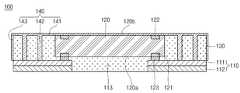
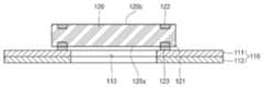
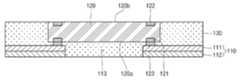
도 1 내지 도 3은 본 발명의 일 실시예에 따른 반도체 패키지의 단면도이다.
도 4는 본 발명의 일 실시예에 따른 비아홀 또는 트렌치의 구조를 나타낸 단면도이다.
도 5는 본 발명의 다른 실시예에 따른 반도체 패키지의 제조 방법을 나타낸 흐름도이다.
도 6 내지 도 13은 본 발명의 다른 실시예에 따른 반도체 패키지의 제조 순서를 나타낸 도면이다.1 to 3 are sectional views of a semiconductor package according to an embodiment of the present invention.
4 is a cross-sectional view illustrating a structure of a via hole or a trench according to an embodiment of the present invention.
5 is a flowchart illustrating a method of manufacturing a semiconductor package according to another embodiment of the present invention.
6 to 13 are diagrams illustrating a manufacturing procedure of a semiconductor package according to another embodiment of the present invention.
이하, 본 발명이 속하는 기술 분야에서 통상의 지식을 가진 자가 본 발명을 용이하게 실시할 수 있을 정도로 본 발명의 바람직한 실시예를 첨부된 도면을 참조하여 상세하게 설명하면 다음과 같다.
DETAILED DESCRIPTION OF THE PREFERRED EMBODIMENTS Hereinafter, preferred embodiments of the present invention will be described in detail with reference to the accompanying drawings, so that those skilled in the art can easily carry out the present invention.
도 1 내지 도 3은 본 발명의 일 실시예에 따른 반도체 패키지의 단면도이다. 도 4는 본 발명의 일 실시예에 따른 비아홀 또는 트렌치의 구조를 나타낸 단면도이다.1 to 3 are sectional views of a semiconductor package according to an embodiment of the present invention. 4 is a cross-sectional view illustrating a structure of a via hole or a trench according to an embodiment of the present invention.
도 1 내지 도 4를 참조하면, 본 발명의 일 실시예에 따른 반도체 패키지(100)는 리드프레임(110), 반도체 다이(120), 몰딩부(130) 및 접지구조체(140)를 포함한다. 더불어, 상기 반도체 패키지(100)는 개재된 히트 슬러그(heat slug) 또는 히트 스프레더(heat spreader)(150)를 더 포함할 수 있다.1 to 4, a
상기 리드프레임(110)은 상기 반도체 다이(120)와 외부 회로를 전기적으로 연결시키며 상기 반도체 다이(120)를 반도체 기판에 고정시켜주는 역할을 한다.The
상기 리드프레임(110)은 구리(Cu)로 이루어진 베이스층(111)과 니켈(Ni), 팔라듐(Pd), 규소(Si), 은(Ag) 또는 이들의 합금으로 이루어진 도금층(112)을 포함할 수 있다.The
상기 리드프레임(110)은 크게 리드커넥터와 접지커넥터로 구성될 수 있으며 관통홀(113)이 형성될 수 있다. 상기 리드커넥터는 상기 반도체 다이(120)의 제1 면(120a)에 형성된 전극패드(121)와 전기적으로 연결되어 상기 반도체 다이(120)와 외부 회로 사이에 전기적인 신호를 전달할 수 있다. 여기서, 상기 전극패드(121)는 솔더볼 또는 솔더범프(123) 등을 통해 상기 리드커넥터와 전기적으로 연결될 수 있다. 상기 접지커넥터는 상기 접지구조체(140)를 통하여 상기 반도체 다이(120)의 제2 면(120b)에 형성된 접지패드(122)와 전기적으로 연결될 수 있다. 상기 관통홀(113)은 상기 반도체 다이(120)의 하부에 형성될 수 있으며, 그 내부에는 상기 몰딩부(130)의 일부가 형성되어 상기 몰딩부(130)가 상기 리드프레임(110)에 잘 고정될 수 있도록 한다.The
상기 반도체 다이(120)는 제1 면(frontside)(120a)과 제2 면(backside)(120b)을 구비할 수 있다. 상기 제2 면(120b)은 상기 제1 면(120a)의 반대 면을 의미한다. 상기 제1 면(120a)에는 상기 전극패드(121)가 형성되며 상기 제2 면(120b)에는 상기 접지패드(122)가 형성될 수 있다.The semiconductor die 120 may have a
상기 몰딩부(130)는 상기 리드프레임(110) 상에 형성되어 상기 반도체 다이(120)의 측부를 둘러쌀 수 있다. 따라서 상기 몰딩부(130)는 상기 리드프레임(110) 상부에는 형성되나 상기 반도체 다이(120)의 제2 면(120b) 상에는 형성되지 않는다. 상기 몰딩부(130)의 일부는 상기 리드프레임(110)의 관통홀(113)에 형성되어 상기 몰딩부(130)가 상기 리드프레임(110)에 견고히 고정될 수 있도록 한다.The
상기 접지구조체(140)는 제1 금속플레이트(141) 및 비아홀 또는 트렌치(142)를 포함할 수 있다. 더불어, 상기 접지구조체(140)는 제2 금속플레이트(143)를 더 포함할 수 있다.The
상기 제1 금속플레이트(141)는 상기 반도체 다이(120)의 제2 면(120b)과 상기 몰딩부(130)의 상면을 덮도록 형성될 수 있다. 따라서 상기 제1 금속플레이트(141)는 상기 반도체 패키지(100)의 상부 전면을 덮도록 형성되어 상기 반도체 다이(120)의 제2 면(120b)의 면적보다 크게 이루어질 수 있다. 또한, 상기 제1 금속플레이트(141)는 상기 반도체 다이(120)의 제2 면(120b)에 형성된 상기 접지패드(122)와 전기적으로 연결될 수 있다.The
상기 비아홀 또는 트렌치(142)는, 상기 몰딩부(130)의 공간이 허용하는 범위 내에서 다수 개로 이루어질 수 있으며, 이들은 각각 상기 제1 금속플레이트(141)로부터 연장되어 상기 몰딩부(130)를 관통하며 상기 리드프레임(110)의 상기 접지커넥터와 전기적으로 연결될 수 있다. 이에 따라 상기 반도체 다이(120)의 상기 접지패드(122)는 상기 제1 금속플레이트(141) 및 상기 비아홀 또는 트렌치(142)를 통해 상기 리드프레임(110)의 상기 접지커넥터와 전기적으로 연결될 수 있다.The via holes or
상기 비아홀 또는 트렌치(142)의 측면은 도 4에 도시된 바와 같이 상기 비아홀 또는 트렌치(142)의 폭이 상기 제1 금속플레이트(141)에서 상기 리드프레임(110) 측으로 갈수록 좁아지는 경사면을 이룰 수 있다(W2>W1). 예를 들어 상기 비아홀 또는 트렌치(142)의 측면은 상기 비아홀 또는 트렌치(142)를 중심축으로 대략 5° 정도 경사진 형태로 이루어질 수 있다. 상기 비아홀 또는 트렌치(142)의 측면이 상기와 같이 경사면으로 이루어진 것은 상기 비아홀 또는 트렌치(142)가 스퍼터링 증착을 통해 형성될 때 상기 비아홀 또는 트렌치(142)의 내벽에 시드층(seed layers)을 좀 더 용이하게 형성하기 위함이다. 상기 비아홀 또는 트렌치(142)의 측면의 경사각이 5° 보다 작은 경우 금속물질이 상기 비아홀 또는 트렌치(142)의 내벽에 쉽게 증착되지 않아 균일한 시드층이 형성되기 어려울 수 있다. 또한 상기 비아홀 또는 트렌치(142)의 측면의 경사각이 5° 보다 큰 경우 상기 비아홀 또는 트렌치(142) 간의 피치(pitch)가 감소되어 상기 비아홀 또는 트렌치(142)의 개수가 줄어들 수 있다. 상기 비아홀 또는 트렌치(142)를 형성할 수 있는 공간이 한정되어 있기 때문에, 동일한 공간 내에 더 많은 상기 비아홀 또는 트렌치(142)를 형성하여 상기 반도체 패키지(100)의 전기적 안정성을 도모하는 것이 바람직하다.As shown in FIG. 4, the side surface of the via hole or the
상기 제2 금속플레이트(143)는 도 2에 도시된 바와 같이 상기 제1 금속플레이트(142)의 가장자리로부터 연장되어 상기 몰딩부(130)의 측면을 덮도록 형성될 수 있다. 상기 반도체 패키지(100)가 4개의 측면을 갖도록 형성되는 경우 상기 제2 금속플레이트(143)는 상기 몰딩부(130)의 적어도 1개의 측면을 덮도록 형성될 수 있다.The
이러한 접지구조체(140)는 금(Au), 은(Ag), 구리(Cu), 티타늄(Ti), 니켈(Ni) 또는 철/니켈/망간(Fe/Ni/Mn) 합금을 포함하여 이루어질 수 있다.This
이와 같이 상기 접지구조체(140)는 상기 리드프레임(110)과 상기 반도체 다이(130)의 접지 사이를 연결함과 동시에 상기 반도체 패키지(100)의 외부를 감싸도록 형성됨으로써 특히 상기 반도체 다이(120)를 둘러싸도록 형성됨으로써 외부로부터 가해지는 EMI(electromagnetic interference)나 기타 간섭 신호 등으로부터 상기 반도체 다이(120)를 안정적으로 보호할 수 있다.The
또한, 상기 제1 금속플레이트(141)는 상기 반도체 다이(110)의 제2 면(120b)과 접촉하며 상기 반도체 다이(110)의 제2 면(120b)보다 넓게 형성됨으로써 상기 반도체 다이(110)로부터 발생되는 열을 보다 용이하게 방출할 수 있다.The
상기 히트 슬러그 또는 히트 스프레더(150)는 도 3에 도시된 바와 같이 상기 제1 금속플레이트(141)와 상기 반도체 다이(120)의 제2 면(120b) 사이에 개재될 수 있다. 이때, 상기 제1 금속플레이트(141)에는 상기 반도체 다이(120)의 제2 면(120b)을 향해 돌출된 돌출부(144)가 형성될 수 있으며, 상기 돌출부(144)는 상기 히트 슬러그 또는 히트 스프레더(150)에 형성된 다수의 홀을 통해 상기 반도체 다이(120)의 접지패드(122)와 전기적으로 연결될 수 있다. 상기 히트 슬러그 또는 히트 스프레더(150)는 상기 반도체 다이(120)에 대한 보다 효율적인 방열이 이루어질 수 있도록 한다.
The heat slug or
도 5는 본 발명의 다른 실시예에 따른 반도체 패키지의 제조 방법을 나타낸 흐름도이다.5 is a flowchart illustrating a method of manufacturing a semiconductor package according to another embodiment of the present invention.
도 5를 참조하면, 본 발명의 다른 실시예에 따른 반도체 패키지의 제조 방법(S500)은 리드프레임 구비 단계(S510), 반도체 다이 연결 단계(S520), 몰딩부 형성 단계(S530) 및 비아홀 또는 트렌치 형성 단계(S540), 접지구조체 형성 단계(S560)를 포함한다. 더불어, 상기 반도체 패키지의 제조 방법(S500)은 상기 비아홀 또는 트렌치 형성 단계(S540)와 상기 접지구조체 형성 단계(S560) 사이에 히트 슬러그 또는 히트 스프레더 부착 단계(S550)를 더 포함할 수 있다.Referring to FIG. 5, a method S500 of manufacturing a semiconductor package according to another embodiment of the present invention includes a step S510 of forming a lead frame, a step S520 of connecting a semiconductor die, a step S530 of forming a molding part, A forming step S540, and a grounding structure forming step S560. In addition, the manufacturing method (S500) of the semiconductor package may further include a step (S550) of attaching a heat slug or a heat spreader between the via hole or trench forming step (S540) and the grounding structure forming step (S560).
도 6 내지 도 13은 본 발명의 다른 실시예에 따른 반도체 패키지의 제조 순서를 나타낸 도면이다.6 to 13 are diagrams illustrating a manufacturing procedure of a semiconductor package according to another embodiment of the present invention.
상기 리드프레임 구비 단계(S510) 및 반도체 다이 연결 단계(S520)에서는, 도 6 및 도 7에 도시된 바와 같이 미리 준비된 리드프레임(110)에 반도체 다이(120)를 전기적으로 연결할 수 있다.6 and 7, the semiconductor die 120 may be electrically connected to the
상기 리드프레임(110)은 상기 반도체 다이(120)와 외부 회로를 전기적으로 연결시키며 상기 반도체 다이(120)를 반도체 기판에 고정시켜주는 역할을 한다.The
상기 리드프레임(110)은 구리(Cu)로 이루어진 베이스층(111)과 니켈(Ni), 팔라듐(Pd), 규소(Si), 은(Ag) 또는 이들의 합금으로 이루어진 도금층(112)을 포함할 수 있다.The
상기 리드프레임(110)은 크게 리드커넥터와 접지커넥터로 구성될 수 있으며 관통홀(113)이 형성될 수 있다. 상기 리드커넥터는 상기 반도체 다이(120)의 제1 면(120a)에 형성된 전극패드(121)와 전기적으로 연결되어 상기 반도체 다이(120)와 외부 회로 사이에 전기적인 신호를 전달할 수 있다. 여기서, 상기 전극패드(121)는 솔더볼 또는 솔더범프(123) 등을 통해 상기 리드커넥터와 전기적으로 연결될 수 있다.The
상기 반도체 다이(120)는 제1 면(frontside)(120a)과 제2 면(backside)(120b)을 구비할 수 있다. 상기 제2 면(120b)은 상기 제1 면(120a)의 반대 면을 의미한다. 상기 제1 면(120a)에는 상기 전극패드(121)가 형성되며 상기 제2 면(120b)에는 접지패드(122)가 형성될 수 있다.The semiconductor die 120 may have a
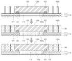
상기 몰딩부 형성 단계(S530)에서는 도 8에 도시된 바와 같이 상기 리드프레임(110) 상에서 상기 반도체 다이(120)의 측부를 둘러싸도록 몰딩부(130)를 형성할 수 있다. 따라서 상기 몰딩부(130)는 상기 리드프레임(110) 상부에는 형성되나 상기 반도체 다이(120)의 제2 면(120b) 상에는 형성되지 않는다. 상기 몰딩부(130)의 일부는 상기 리드프레임(110)의 관통홀(113)에 형성되어 상기 몰딩부(130)가 상기 리드프레임(110)에 견고히 고정될 수 있도록 한다.In the molding part formation step S530, the
상기 비아홀 또는 트렌치 형성 단계(S540)에서는 레이저 식각을 이용하여 도 9a에 도시된 바와 같이 상기 몰딩부(130)를 관통하여 상기 리드프레임(110)의 접지커넥터와 연결되는 다수의 비아홀 또는 트렌치(142a)를 형성할 수 있다. 여기서 비아홀 또는 트렌치(142a)는 금속물질이 충전되기 전 상기 몰딩부(130)에 패터닝된 빈 공간을 의미할 수 있다.In the via hole or trench formation step S540, a plurality of via holes or
또한 상기 비아홀 또는 트렌치 형성 단계(S540)에서는 레이저 식각 뿐만 아니라 도 9b에 도시된 바와 같이 상기 몰딩부(130)를 형성하기 전에 비아홀 또는 트렌치(142a)와 대응하는 패턴 구조체(142b)를 배치시키고 상기 몰딩부(130)를 형성한 후에 상기 패턴 구조체(142b)를 제거하는 방식으로 다수의 비아홀 또는 트렌치(142a)를 형성할 수도 있다.In the via hole or trench formation step S540, not only the laser etching but also the
상기 비아홀 또는 트렌치(142a)의 측면은 도 10에 도시된 바와 같이 상기 비아홀 또는 트렌치(142a)의 폭이 상기 리드프레임(110) 측으로 갈수록 좁아지는 경사면을 이룰 수 있다(W2>W1). 예를 들어 상기 비아홀 또는 트렌치(142a)의 측면은 상기 비아홀 또는 트렌치(142a)를 중심축으로 대략 5° 정도 경사진 형태로 이루어질 수 있다. 상기 비아홀 또는 트렌치(142a)의 측면이 상기와 같이 경사면으로 이루어진 것은 상기 비아홀 또는 트렌치(142a)가 스퍼터링 증착을 통해 형성될 때 상기 비아홀 또는 트렌치(142a)의 내벽에 시드층(seed layers)을 좀 더 용이하게 형성하기 위함이다. 상기 비아홀 또는 트렌치(14a2)의 측면의 경사각이 5° 보다 작은 경우 금속물질이 상기 비아홀 또는 트렌치(142a)의 내벽에 쉽게 증착되지 않아 균일한 시드층이 형성되기 어려울 수 있다. 또한 상기 비아홀 또는 트렌치(142a)의 측면의 경사각이 5° 보다 큰 경우 상기 비아홀 또는 트렌치(142a) 간의 피치(pitch)가 감소되어 상기 비아홀 또는 트렌치(142a)의 개수가 줄어들 수 있다. 상기 비아홀 또는 트렌치(142a)를 형성할 수 있는 공간이 한정되어 있기 때문에, 동일한 공간 내에 더 많은 상기 비아홀 또는 트렌치(142a)를 형성하여 반도체 패키지의 전기적 안정성을 도모하는 것이 바람직하다.As shown in FIG. 10, the side surface of the via hole or the
상기 히트 슬러그 또는 히트 스프레더 부착 단계(S550)에서는 도 11에 도시된 바와 같이 상기 반도체 다이(120)의 제2 면(120b) 상에 히트 슬러그(heat slug) 또는 히트 스프레더(heat spreader)(150)를 부착할 수 있다. 상기 히트 슬러그 또는 히트 스프레더(150)에는 상기 반도체 다이(120)의 접지패드(122)와 대응하는 다수의 홀(150a)이 형성될 수 있다. 이러한 히트 슬러그 또는 히트 스프레더 부착 단계(S550)는 생략될 수도 있다.A heat slug or a
상기 접지구조체 형성 단계(S560)에서는 도 12a에 도시된 바와 같이 스퍼터링 증착을 통해 소정의 금속물질로 상기 비아홀 또는 트렌치(142a) 내부를 충진시키고 상기 반도체 다이(120)의 제2 면(120b) 및 상기 몰딩부(130)의 상면을 덮도록 증착시켜 접지구조체(140)를 형성할 수 있다. 상기 금속물질은 금(Au), 은(Ag), 구리(Cu), 티타늄(Ti), 니켈(Ni) 또는 철/니켈/망간(Fe/Ni/Mn) 합금을 포함할 수 있다.12A, the via hole or
이에 따라 상기 접지구조체(140)는 상기 금속물질이 상기 비아홀 또는 트렌치(142a) 내부에 충진되어 상기 리드프레임(110)의 접지커넥터와 전기적으로 연결된 비아홀 또는 트렌치(142), 상기 금속물질이 상기 반도체 다이의 제2 면(120b) 및 상기 몰딩부(130)의 상면에 증착되어 형성된 제1 금속플레이트(141), 및 상기 금속물질이 상기 히트 슬러그 또는 히트 스프레더(150)의 홀(150a)에 충진되어 상기 제1 금속플레이트(141)로부터 돌출된 형태로 형성되며 상기 반도체 다이(120)의 접지패드(122)와 전기적으로 연결되는 돌출부(144)로 이루어질 수 있다. 이와 같이 형성된 상기 접지구조체(140)는 상기 리드프레임(110)의 접지커넥터와 상기 반도체 다이(120) 접지패드(122) 사이를 전기적으로 연결할 수 있다.Accordingly, the
또한, 상기 접지구조체 형성 단계(S560)에서는 도 12b에 도시된 바와 같이 상기 비아홀 또는 트렌치(142a) 내면과 상기 반도체 다이(120)의 제2 면(120b) 및 상기 몰딩부(130)의 상면에 각각 시드층(140a)을 형성한 후, 전기 도금을 통해 상기 시드층(140a)을 도금하는 방식으로 상기 접지구조체(140)를 형성할 수도 있다.12B, the inner surface of the via hole or the
이후, 상기 접지구조체 형성 단계(S560)에서는 도 13에 도시된 바와 같이 스퍼터링 증착을 통해 상기 제1 금속플레이트(142)의 가장자리로부터 연장되어 상기 몰딩부(130)의 측면을 덮는 제2 금속플레이트(143)를 더 형성할 수 있다. 상기 제2 금속플레이트(143)는 상기 제1 금속플레이트(141)의 면적을 좀 더 확장하기 위한 것으로 상기 리드프레임(110)과 접촉되지 않도록 형성하는 것이 바람직하다.
13, a second metal plate (not shown) extending from the edge of the
이상에서 설명한 것은 본 발명에 따른 반도체 패키지 및 반도체 패키지의 제조 방법을 실시하기 위한 실시예에 불과한 것으로, 본 발명은 상기한 실시예에 한정되지 않고, 본 발명의 기술적 요지를 벗어나지 아니하는 범위 내에서 다양하게 실시될 수 있음은 본 발명이 속하는 기술분야에서 통상의 지식을 가진 자에 있어서 자명한 것이다.
It is to be understood that the present invention is not limited to the above-described embodiments, and various modifications and changes may be made without departing from the scope of the present invention. It will be apparent to those skilled in the art that various changes and modifications may be made without departing from the scope of the present invention.
100: 반도체 패키지111: 베이스층
112: 도금층113: 관통홀
120: 반도체 다이120a: 제1 면
120b: 제2 면121: 전극패드
122: 접지패드123: 솔더볼/솔더범프
130: 몰딩부140: 접지구조체
141: 제1 금속플레이트142: 비아홀 또는 트렌치
143: 제2 금속플레이트144: 돌출부
150: 히트 슬러그/히트 스프레더150a: 홀100: semiconductor package 111: base layer
112: Plated layer 113: Through hole
120:
120b: second surface 121: electrode pad
122: grounding pad 123: solder ball / solder bump
130: molding part 140: grounding structure
141: first metal plate 142: via hole or trench
143: second metal plate 144:
150: heat slug /
Claims (20)
Translated fromKorean제1 면을 통해 상기 리드프레임과 전기적으로 연결된 반도체 다이;
상기 리드프레임 상에 형성되어 상기 반도체 다이의 측부를 둘러싸는 몰딩부; 및
상기 제1 면의 반대 면인 상기 반도체 다이의 제2 면과 상기 몰딩부의 상면을 덮으며 상기 제2 면을 통해 상기 반도체 다이의 접지패드와 전기적으로 연결된 제1 금속플레이트, 및 상기 제1 금속플레이트로부터 상기 몰딩부를 관통하도록 연장되어 상기 리드프레임의 접지커넥터와 전기적으로 연결된 비아홀 또는 트렌치를 포함하는 접지구조체를 포함하며,
상기 비아홀 또는 트렌치의 측면은, 상기 비아홀 또는 트렌치의 폭이 상기 리드프레임 측으로 갈수록 좁아지는 경사면을 이루는 것을 특징으로 하는 반도체 패키지.Lead frame;
A semiconductor die electrically connected to the lead frame through a first surface;
A molding part formed on the lead frame and surrounding the side of the semiconductor die; And
A first metal plate overlying a second surface of the semiconductor die and an upper surface of the molding portion opposite the first surface and electrically connected to a ground pad of the semiconductor die through the second surface, And a ground structure extending through the molding portion and including a via hole or trench electrically connected to a ground connector of the lead frame,
Wherein a side surface of the via hole or the trench forms an inclined surface in which the width of the via hole or the trench becomes narrower toward the lead frame side.
상기 접지구조체는 상기 제1 금속플레이트로부터 상기 몰딩부의 측면으로 연장된 제2 금속플레이트를 더 포함하는 것을 특징으로 하는 반도체 패키지.The method according to claim 1,
Wherein the ground structure further comprises a second metal plate extending from the first metal plate to a side of the molding portion.
상기 제1 금속플레이트와 상기 제2 면 사이에 개재된 히트 슬러그(heat slug) 또는 히트 스프레더(heat spreader)를 더 포함하는 것을 특징으로 하는 반도체 패키지.The method according to claim 1,
Further comprising a heat slug or a heat spreader interposed between the first metal plate and the second surface.
상기 제1 금속플레이트의 면적은 상기 제2 면의 면적보다 넓게 이루어진 것을 특징으로 하는 반도체 패키지.The method according to claim 1,
Wherein an area of the first metal plate is larger than an area of the second surface.
상기 접지구조체는 Au, Ag, Cu, Ti, Ni 또는 Fe/Ni/Mn 합금을 포함하는 것을 특징으로 하는 반도체 패키지.The method according to claim 1,
Wherein the ground structure comprises Au, Ag, Cu, Ti, Ni or an Fe / Ni / Mn alloy.
상기 비아홀 또는 트렌치를 중심축으로 5° 경사진 것을 특징으로 하는 반도체 패키지.The method according to claim 1,
Wherein the via hole or the trench is inclined 5 占 about the center axis.
반도체 다이의 제1 면을 상기 리드프레임과 전기적으로 연결하는 단계;
상기 반도체 다이의 측부를 둘러싸도록 상기 리드프레임 상에 몰딩부를 형성하는 단계;
상기 몰딩부를 관통하여 상기 리드프레임의 접지커넥터와 연결되는 비아홀 또는 트렌치를 형성하는 단계; 및
스퍼터링 증착을 통해 소정의 금속물질로 상기 비아홀 또는 트렌치 내부를 충진시키고 상기 제1 면의 반대 면으로서 접지패드가 형성된 상기 반도체 다이의 제2 면 및 상기 몰딩부의 상면을 덮도록 각각 증착시켜, 상기 접지커넥터와 상기 접지패드 사이를 전기적으로 연결하는 접지구조체를 형성하는 단계를 포함하고,
상기 비아홀 또는 트렌치를 형성하는 단계에서, 상기 비아홀 또는 트렌치의 측면은 상기 비아홀 또는 트렌치의 폭이 상기 리드프레임 측으로 갈수록 좁아지는 경사면을 이루도록 형성하는 것을 특징으로 하는 반도체 패키지의 제조 방법.Providing a lead frame;
Electrically connecting a first side of the semiconductor die to the lead frame;
Forming a molding on the lead frame to surround a side of the semiconductor die;
Forming a via hole or a trench through the molding portion and connected to the ground connector of the lead frame; And
Filling the via hole or trench with a predetermined metal material through sputtering deposition and depositing the second surface of the semiconductor die on which the ground pad is formed as an opposite surface of the first surface and the upper surface of the molding portion respectively, And forming a ground structure that electrically connects the connector and the ground pad,
Wherein the side surfaces of the via hole or the trench are formed to be inclined so that the width of the via hole or the trench becomes narrower toward the lead frame side in the step of forming the via hole or the trench.
상기 접지구조체를 형성하는 단계에서, 상기 스퍼터링 증착을 통해 상기 금속물질을 상기 몰딩부의 측면에 증착하는 단계를 더 포함하는 것을 특징으로 하는 반도체 패키지의 제조 방법.8. The method of claim 7,
Further comprising the step of depositing the metal material on a side surface of the molding portion through the sputtering deposition in the step of forming the grounding structure.
상기 비아홀 또는 트렌치를 형성하는 단계 및 상기 접지구조체를 형성하는 단계 사이에, 상기 반도체 다이의 제2 면에 히트 슬러그(heat slug) 또는 히트 스프레더(heat spreader)를 부착하는 단계를 더 포함하는 것을 특징으로 하는 반도체 패키지의 제조 방법.8. The method of claim 7,
Further comprising the step of attaching a heat slug or a heat spreader to the second surface of the semiconductor die between the step of forming the via hole or trench and the step of forming the grounding structure Wherein said semiconductor package is a semiconductor package.
상기 비아홀 또는 트렌치를 형성하는 단계에서 상기 비아홀 또는 트렌치는 레이저 식각을 통해 형성하는 것을 특징으로 하는 반도체 패키지의 제조 방법.8. The method of claim 7,
Wherein the via hole or the trench is formed through laser etching in the step of forming the via hole or the trench.
상기 비아홀 또는 트렌치를 형성하는 단계에서 상기 비아홀 또는 트렌치는, 상기 몰딩부를 형성하기 전에 상기 비아홀 또는 트렌치 패턴을 미리 배치하고 상기 몰딩부를 형성한 후 상기 비아홀 또는 트렌치 패턴을 제거하여 형성하는 것을 특징으로 하는 반도체 패키지의 제조 방법.8. The method of claim 7,
Wherein the via hole or the trench is formed by previously arranging the via hole or the trench pattern before forming the molding part and removing the via hole or the trench pattern after forming the molding part in the step of forming the via hole or the trench A method of manufacturing a semiconductor package.
상기 금속물질은 Au, Ag, Cu, Ti, Ni 또는 Fe/Ni/Mn 합금을 포함하는 것을 특징으로 하는 반도체 패키지의 제조 방법.8. The method of claim 7,
Wherein the metal material comprises Au, Ag, Cu, Ti, Ni, or Fe / Ni / Mn alloy.
상기 비아홀 또는 트렌치의 측면은 상기 비아홀 또는 트렌치를 중심축으로 5° 경사진 것을 특징으로 하는 반도체 패키지의 제조 방법.8. The method of claim 7,
Wherein a side surface of the via hole or the trench is inclined at 5 DEG with respect to the via hole or the trench as a center axis.
반도체 다이의 제1 면을 상기 리드프레임과 전기적으로 연결하는 단계;
상기 반도체 다이의 측부를 둘러싸도록 상기 리드프레임 상에 몰딩부를 형성하는 단계;
상기 몰딩부를 관통하여 상기 리드프레임의 접지커넥터와 연결되는 비아홀 또는 트렌치를 형성하는 단계; 및
스퍼터링 증착을 통해 소정의 금속물질로 상기 비아홀 또는 트렌치 내면과 상기 제1 면의 반대 면으로서 접지패드가 형성된 상기 반도체 다이의 제2 면 및 상기 몰딩부의 상면에 각각 시드층을 형성한 후, 전기 도금을 통해 상기 시드층을 도금하여 상기 접지커넥터와 상기 접지패드 사이를 전기적으로 연결하는 접지구조체를 형성하는 단계를 포함하며,
상기 비아홀 또는 트렌치를 형성하는 단계에서, 상기 비아홀 또는 트렌치의 측면은 상기 비아홀 또는 트렌치의 폭이 상기 리드프레임 측으로 갈수록 좁아지는 경사면을 이루도록 형성하는 것을 특징으로 하는 반도체 패키지의 제조 방법.Providing a lead frame;
Electrically connecting a first side of the semiconductor die to the lead frame;
Forming a molding on the lead frame to surround a side of the semiconductor die;
Forming a via hole or a trench through the molding portion and connected to the ground connector of the lead frame; And
A seed layer is formed on the second surface of the semiconductor die and the upper surface of the molding portion where a ground pad is formed as a surface opposite to the inner surface of the via hole or trench and the first surface with a predetermined metal material through sputter deposition, And forming a ground structure that electrically connects the grounding connector and the grounding pad by plating the seed layer through the grounding structure,
Wherein the side surfaces of the via hole or the trench are formed to be inclined so that the width of the via hole or the trench becomes narrower toward the lead frame side in the step of forming the via hole or the trench.
상기 접지구조체를 형성하는 단계에서, 상기 스퍼터링 증착을 통해 상기 금속물질로 상기 몰딩부의 측면에 시드층을 형성한 후 상기 전기 도금을 통해 상기 몰딩부의 측면에 형성된 시드층의 표면을 도금하는 단계를 더 포함하는 것을 특징으로 하는 반도체 패키지의 제조 방법.15. The method of claim 14,
Forming a seed layer on the side surface of the molding portion with the metal material through the sputtering deposition and plating the surface of the seed layer formed on the side surface of the molding portion through the electroplating, Wherein the step of forming the semiconductor package comprises the steps of:
상기 비아홀 또는 트렌치를 형성하는 단계 및 상기 접지구조체를 형성하는 단계 사이에, 상기 반도체 다이의 제2 면에 히트 슬러그(heat slug) 또는 히트 스프레더(heat spreader)를 부착하는 단계를 더 포함하는 것을 특징으로 하는 반도체 패키지의 제조 방법.15. The method of claim 14,
Further comprising the step of attaching a heat slug or a heat spreader to the second surface of the semiconductor die between the step of forming the via hole or trench and the step of forming the grounding structure Wherein said semiconductor package is a semiconductor package.
상기 비아홀 또는 트렌치를 형성하는 단계에서 상기 비아홀 또는 트렌치는 레이저 식각을 통해 형성하는 것을 특징으로 하는 반도체 패키지의 제조 방법.15. The method of claim 14,
Wherein the via hole or the trench is formed through laser etching in the step of forming the via hole or the trench.
상기 비아홀 또는 트렌치를 형성하는 단계에서 상기 비아홀 또는 트렌치는, 상기 몰딩부를 형성하기 전에 상기 비아홀 또는 트렌치 패턴을 미리 배치하고 상기 몰딩부를 형성한 후 상기 비아홀 또는 트렌치 패턴을 제거하여 형성하는 것을 특징으로 하는 반도체 패키지의 제조 방법.15. The method of claim 14,
Wherein the via hole or the trench is formed by previously arranging the via hole or the trench pattern before forming the molding part and removing the via hole or the trench pattern after forming the molding part in the step of forming the via hole or the trench A method of manufacturing a semiconductor package.
상기 금속물질은 Au, Ag, Cu, Ti, Ni 또는 Fe/Ni/Mn 합금을 포함하는 것을 특징으로 하는 반도체 패키지의 제조 방법.15. The method of claim 14,
Wherein the metal material comprises Au, Ag, Cu, Ti, Ni, or Fe / Ni / Mn alloy.
상기 비아홀 또는 트렌치의 측면은 상기 비아홀 또는 트렌치를 중심축으로 5° 경사진 것을 특징으로 하는 반도체 패키지의 제조 방법.15. The method of claim 14,
Wherein a side surface of the via hole or the trench is inclined at 5 DEG with respect to the via hole or the trench as a center axis.
Priority Applications (1)
| Application Number | Priority Date | Filing Date | Title |
|---|---|---|---|
| KR1020150014264AKR101672619B1 (en) | 2015-01-29 | 2015-01-29 | Semiconductor package and methods for manufacturing the semiconductor package |
Applications Claiming Priority (1)
| Application Number | Priority Date | Filing Date | Title |
|---|---|---|---|
| KR1020150014264AKR101672619B1 (en) | 2015-01-29 | 2015-01-29 | Semiconductor package and methods for manufacturing the semiconductor package |
Publications (2)
| Publication Number | Publication Date |
|---|---|
| KR20160093365A KR20160093365A (en) | 2016-08-08 |
| KR101672619B1true KR101672619B1 (en) | 2016-11-03 |
Family
ID=56711838
Family Applications (1)
| Application Number | Title | Priority Date | Filing Date |
|---|---|---|---|
| KR1020150014264AActiveKR101672619B1 (en) | 2015-01-29 | 2015-01-29 | Semiconductor package and methods for manufacturing the semiconductor package |
Country Status (1)
| Country | Link |
|---|---|
| KR (1) | KR101672619B1 (en) |
Cited By (1)
| Publication number | Priority date | Publication date | Assignee | Title |
|---|---|---|---|---|
| US12119288B2 (en) | 2021-06-29 | 2024-10-15 | Samsung Electronics Co., Ltd. | Semiconductor package |
Families Citing this family (1)
| Publication number | Priority date | Publication date | Assignee | Title |
|---|---|---|---|---|
| KR101870153B1 (en)* | 2016-11-28 | 2018-06-25 | 주식회사 네패스 | Semiconductor Package of using Insulating Frame and Method of fabricating the same |
Citations (4)
| Publication number | Priority date | Publication date | Assignee | Title |
|---|---|---|---|---|
| US7618846B1 (en)* | 2008-06-16 | 2009-11-17 | Stats Chippac, Ltd. | Semiconductor device and method of forming shielding along a profile disposed in peripheral region around the device |
| US20120049334A1 (en) | 2010-08-27 | 2012-03-01 | Stats Chippac, Ltd. | Semiconductor Device and Method of Forming Leadframe as Vertical Interconnect Structure Between Stacked Semiconductor Die |
| US8169058B2 (en)* | 2009-08-21 | 2012-05-01 | Stats Chippac, Ltd. | Semiconductor device and method of stacking die on leadframe electrically connected by conductive pillars |
| US8916968B2 (en) | 2012-03-27 | 2014-12-23 | Infineon Technologies Ag | Multichip power semiconductor device |
- 2015
- 2015-01-29KRKR1020150014264Apatent/KR101672619B1/enactiveActive
Patent Citations (4)
| Publication number | Priority date | Publication date | Assignee | Title |
|---|---|---|---|---|
| US7618846B1 (en)* | 2008-06-16 | 2009-11-17 | Stats Chippac, Ltd. | Semiconductor device and method of forming shielding along a profile disposed in peripheral region around the device |
| US8169058B2 (en)* | 2009-08-21 | 2012-05-01 | Stats Chippac, Ltd. | Semiconductor device and method of stacking die on leadframe electrically connected by conductive pillars |
| US20120049334A1 (en) | 2010-08-27 | 2012-03-01 | Stats Chippac, Ltd. | Semiconductor Device and Method of Forming Leadframe as Vertical Interconnect Structure Between Stacked Semiconductor Die |
| US8916968B2 (en) | 2012-03-27 | 2014-12-23 | Infineon Technologies Ag | Multichip power semiconductor device |
Cited By (1)
| Publication number | Priority date | Publication date | Assignee | Title |
|---|---|---|---|---|
| US12119288B2 (en) | 2021-06-29 | 2024-10-15 | Samsung Electronics Co., Ltd. | Semiconductor package |
Also Published As
| Publication number | Publication date |
|---|---|
| KR20160093365A (en) | 2016-08-08 |
Similar Documents
| Publication | Publication Date | Title |
|---|---|---|
| KR100709662B1 (en) | Semiconductor device and manufacturing method thereof | |
| JP4512101B2 (en) | Manufacturing method of semiconductor chip | |
| KR102198629B1 (en) | Embedded packaging with preformed vias | |
| CN208923115U (en) | A kind of encapsulating structure of Microwave Multichip Module | |
| CN104851812B (en) | Semiconductor element and manufacturing method thereof | |
| US9362209B1 (en) | Shielding technique for semiconductor package including metal lid | |
| CN101916754B (en) | Via hole and via hole forming method and via hole filling method | |
| US20050017358A1 (en) | Semiconductor component having conductors with wire bondable metalization layers | |
| KR101218989B1 (en) | Semiconductor package and manufacturing method thereof | |
| KR20020044590A (en) | Metal redistribution layer having solderable pads and wire bondable pads | |
| US8125064B1 (en) | Increased I/O semiconductor package and method of making same | |
| US10217710B2 (en) | Wiring board with embedded component and integrated stiffener, method of making the same and face-to-face semiconductor assembly using the same | |
| CN110223971A (en) | Dimensional stackable formula semiconductor group body with heat dissipation characteristics | |
| US12412845B2 (en) | Semiconductor packages and methods of manufacturing the same | |
| KR20160020566A (en) | Method of forming a microelectronic assembly by plating metal connectors after assemblying first and second components and corresponding device | |
| KR101672619B1 (en) | Semiconductor package and methods for manufacturing the semiconductor package | |
| JP4511148B2 (en) | Manufacturing method of semiconductor device | |
| US9443837B2 (en) | Z-connection for a microelectronic package using electroless plating | |
| US7821134B2 (en) | Semiconductor device, electronic device and fabrication method of the same | |
| US11791293B2 (en) | Semiconductor device and method of manufacturing the same | |
| KR20240168588A (en) | Semiconductor Die Having a Metal Plate Layer | |
| US20180122721A1 (en) | Plug structure of a semiconductor chip and method of manufacturing the same | |
| WO2012111722A1 (en) | Semiconductor chip and semiconductor device | |
| TWI690031B (en) | Wiring board having component integrated with leadframe and method of making the same | |
| US7605475B2 (en) | Semiconductor device |
Legal Events
| Date | Code | Title | Description |
|---|---|---|---|
| A201 | Request for examination | ||
| PA0109 | Patent application | St.27 status event code:A-0-1-A10-A12-nap-PA0109 | |
| PA0201 | Request for examination | St.27 status event code:A-1-2-D10-D11-exm-PA0201 | |
| D13-X000 | Search requested | St.27 status event code:A-1-2-D10-D13-srh-X000 | |
| D14-X000 | Search report completed | St.27 status event code:A-1-2-D10-D14-srh-X000 | |
| E902 | Notification of reason for refusal | ||
| PE0902 | Notice of grounds for rejection | St.27 status event code:A-1-2-D10-D21-exm-PE0902 | |
| P11-X000 | Amendment of application requested | St.27 status event code:A-2-2-P10-P11-nap-X000 | |
| P13-X000 | Application amended | St.27 status event code:A-2-2-P10-P13-nap-X000 | |
| PG1501 | Laying open of application | St.27 status event code:A-1-1-Q10-Q12-nap-PG1501 | |
| E701 | Decision to grant or registration of patent right | ||
| PE0701 | Decision of registration | St.27 status event code:A-1-2-D10-D22-exm-PE0701 | |
| PR0701 | Registration of establishment | St.27 status event code:A-2-4-F10-F11-exm-PR0701 | |
| PR1002 | Payment of registration fee | St.27 status event code:A-2-2-U10-U11-oth-PR1002 Fee payment year number:1 | |
| PG1601 | Publication of registration | St.27 status event code:A-4-4-Q10-Q13-nap-PG1601 | |
| PN2301 | Change of applicant | St.27 status event code:A-5-5-R10-R13-asn-PN2301 St.27 status event code:A-5-5-R10-R11-asn-PN2301 | |
| P22-X000 | Classification modified | St.27 status event code:A-4-4-P10-P22-nap-X000 | |
| FPAY | Annual fee payment | Payment date:20191008 Year of fee payment:4 | |
| PR1001 | Payment of annual fee | St.27 status event code:A-4-4-U10-U11-oth-PR1001 Fee payment year number:4 | |
| PR1001 | Payment of annual fee | St.27 status event code:A-4-4-U10-U11-oth-PR1001 Fee payment year number:5 | |
| PR1001 | Payment of annual fee | St.27 status event code:A-4-4-U10-U11-oth-PR1001 Fee payment year number:6 | |
| PR1001 | Payment of annual fee | St.27 status event code:A-4-4-U10-U11-oth-PR1001 Fee payment year number:7 | |
| PR1001 | Payment of annual fee | St.27 status event code:A-4-4-U10-U11-oth-PR1001 Fee payment year number:8 | |
| PR1001 | Payment of annual fee | St.27 status event code:A-4-4-U10-U11-oth-PR1001 Fee payment year number:9 | |
| PR1001 | Payment of annual fee | St.27 status event code:A-4-4-U10-U11-oth-PR1001 Fee payment year number:10 |