KR101669720B1 - Magnetoresistive random access memory structure and method of forming the same - Google Patents
Magnetoresistive random access memory structure and method of forming the sameDownload PDFInfo
- Publication number
- KR101669720B1 KR101669720B1KR1020140086227AKR20140086227AKR101669720B1KR 101669720 B1KR101669720 B1KR 101669720B1KR 1020140086227 AKR1020140086227 AKR 1020140086227AKR 20140086227 AKR20140086227 AKR 20140086227AKR 101669720 B1KR101669720 B1KR 101669720B1
- Authority
- KR
- South Korea
- Prior art keywords
- layer
- ferromagnetic
- ferromagnetic free
- electrode structure
- free layer
- Prior art date
- Legal status (The legal status is an assumption and is not a legal conclusion. Google has not performed a legal analysis and makes no representation as to the accuracy of the status listed.)
- Active
Links
Images


Classifications
- H—ELECTRICITY
- H10—SEMICONDUCTOR DEVICES; ELECTRIC SOLID-STATE DEVICES NOT OTHERWISE PROVIDED FOR
- H10N—ELECTRIC SOLID-STATE DEVICES NOT OTHERWISE PROVIDED FOR
- H10N50/00—Galvanomagnetic devices
- H10N50/10—Magnetoresistive devices
- G—PHYSICS
- G11—INFORMATION STORAGE
- G11C—STATIC STORES
- G11C11/00—Digital stores characterised by the use of particular electric or magnetic storage elements; Storage elements therefor
- G11C11/02—Digital stores characterised by the use of particular electric or magnetic storage elements; Storage elements therefor using magnetic elements
- G11C11/14—Digital stores characterised by the use of particular electric or magnetic storage elements; Storage elements therefor using magnetic elements using thin-film elements
- G11C11/15—Digital stores characterised by the use of particular electric or magnetic storage elements; Storage elements therefor using magnetic elements using thin-film elements using multiple magnetic layers
- G—PHYSICS
- G11—INFORMATION STORAGE
- G11C—STATIC STORES
- G11C11/00—Digital stores characterised by the use of particular electric or magnetic storage elements; Storage elements therefor
- G11C11/02—Digital stores characterised by the use of particular electric or magnetic storage elements; Storage elements therefor using magnetic elements
- G11C11/16—Digital stores characterised by the use of particular electric or magnetic storage elements; Storage elements therefor using magnetic elements using elements in which the storage effect is based on magnetic spin effect
- G11C11/161—Digital stores characterised by the use of particular electric or magnetic storage elements; Storage elements therefor using magnetic elements using elements in which the storage effect is based on magnetic spin effect details concerning the memory cell structure, e.g. the layers of the ferromagnetic memory cell
- H—ELECTRICITY
- H10—SEMICONDUCTOR DEVICES; ELECTRIC SOLID-STATE DEVICES NOT OTHERWISE PROVIDED FOR
- H10B—ELECTRONIC MEMORY DEVICES
- H10B61/00—Magnetic memory devices, e.g. magnetoresistive RAM [MRAM] devices
- H—ELECTRICITY
- H10—SEMICONDUCTOR DEVICES; ELECTRIC SOLID-STATE DEVICES NOT OTHERWISE PROVIDED FOR
- H10B—ELECTRONIC MEMORY DEVICES
- H10B61/00—Magnetic memory devices, e.g. magnetoresistive RAM [MRAM] devices
- H10B61/20—Magnetic memory devices, e.g. magnetoresistive RAM [MRAM] devices comprising components having three or more electrodes, e.g. transistors
- H10B61/22—Magnetic memory devices, e.g. magnetoresistive RAM [MRAM] devices comprising components having three or more electrodes, e.g. transistors of the field-effect transistor [FET] type
- H—ELECTRICITY
- H10—SEMICONDUCTOR DEVICES; ELECTRIC SOLID-STATE DEVICES NOT OTHERWISE PROVIDED FOR
- H10D—INORGANIC ELECTRIC SEMICONDUCTOR DEVICES
- H10D86/00—Integrated devices formed in or on insulating or conducting substrates, e.g. formed in silicon-on-insulator [SOI] substrates or on stainless steel or glass substrates
- H10D86/40—Integrated devices formed in or on insulating or conducting substrates, e.g. formed in silicon-on-insulator [SOI] substrates or on stainless steel or glass substrates characterised by multiple TFTs
- H10D86/421—Integrated devices formed in or on insulating or conducting substrates, e.g. formed in silicon-on-insulator [SOI] substrates or on stainless steel or glass substrates characterised by multiple TFTs having a particular composition, shape or crystalline structure of the active layer
- H—ELECTRICITY
- H10—SEMICONDUCTOR DEVICES; ELECTRIC SOLID-STATE DEVICES NOT OTHERWISE PROVIDED FOR
- H10D—INORGANIC ELECTRIC SEMICONDUCTOR DEVICES
- H10D86/00—Integrated devices formed in or on insulating or conducting substrates, e.g. formed in silicon-on-insulator [SOI] substrates or on stainless steel or glass substrates
- H10D86/40—Integrated devices formed in or on insulating or conducting substrates, e.g. formed in silicon-on-insulator [SOI] substrates or on stainless steel or glass substrates characterised by multiple TFTs
- H10D86/60—Integrated devices formed in or on insulating or conducting substrates, e.g. formed in silicon-on-insulator [SOI] substrates or on stainless steel or glass substrates characterised by multiple TFTs wherein the TFTs are in active matrices
- H—ELECTRICITY
- H10—SEMICONDUCTOR DEVICES; ELECTRIC SOLID-STATE DEVICES NOT OTHERWISE PROVIDED FOR
- H10N—ELECTRIC SOLID-STATE DEVICES NOT OTHERWISE PROVIDED FOR
- H10N50/00—Galvanomagnetic devices
- H10N50/01—Manufacture or treatment
- H—ELECTRICITY
- H10—SEMICONDUCTOR DEVICES; ELECTRIC SOLID-STATE DEVICES NOT OTHERWISE PROVIDED FOR
- H10N—ELECTRIC SOLID-STATE DEVICES NOT OTHERWISE PROVIDED FOR
- H10N50/00—Galvanomagnetic devices
- H10N50/80—Constructional details
Landscapes
- Engineering & Computer Science (AREA)
- Computer Hardware Design (AREA)
- Manufacturing & Machinery (AREA)
- Mram Or Spin Memory Techniques (AREA)
- Hall/Mr Elements (AREA)
- Chemical & Material Sciences (AREA)
- Crystallography & Structural Chemistry (AREA)
Abstract
Translated fromKoreanDescription
Translated fromKorean일반적으로, 본 발명개시는 반도체 구조물에 관한 것이며, 보다 구체적으로는, 자기저항 랜덤 액세스 메모리 구조물 및 자기저항 랜덤 액세스 메모리 구조물을 형성하는 방법에 관한 것이다.In general, the disclosure relates to semiconductor structures, and more particularly, to magnetoresistive random access memory structures and methods of forming magnetoresistive random access memory structures.
집적 회로(integrated circuit; IC) 디바이스들에서, 자기저항 랜덤 액세스 메모리(magnetoresistive random access memory; MRAM)는 다음 세대의 비휘발성 메모리 디바이스들을 위한 신흥 기술이다. MRAM은 MRAM 셀들의 어레이를 포함하는 메모리 구조물이다. 각각의 셀에서의 데이터 비트는 전하보다는, 저항을 이용하여 판독이 된다. 특히, 각각의 MRAM 셀은 자기 터널 접합(magnetic tunnel junction; MTJ) 엘리먼트를 포함하며, MTJ 엘리먼트의 저항은 논리 "0" 또는 논리 "1"을 표현하기 위해 조정가능하다. MTJ 엘리먼트는 터널링 절연층에 의해 분리된 하나의 강자성(ferromagnetic) 고정층과 하나의 강자성 자유층을 포함한다. MTJ 엘리먼트의 저항은 강자성 고정층의 자기 모멘트의 방향에 대하여 강자성 자유층의 자기 모멘트의 방향을 변경시킴으로써 조정이 된다. 디지털 신호 "1" 또는 "0"을 표시하기 위해 로우 저항 및 하이 저항이 활용되며, 이로써 데이터 저장을 가능케 한다.BACKGROUND OF THE INVENTION In integrated circuit (IC) devices, magnetoresistive random access memory (MRAM) is an emerging technology for the next generation of non-volatile memory devices. An MRAM is a memory structure that includes an array of MRAM cells. The data bits in each cell are read using a resistor rather than a charge. In particular, each MRAM cell includes a magnetic tunnel junction (MTJ) element, and the resistance of the MTJ element is adjustable to represent a logic "0" or a logic "1 ". The MTJ element includes one ferromagnetic pinned layer separated by a tunneling insulating layer and one ferromagnetic free layer. The resistance of the MTJ element is adjusted by changing the direction of the magnetic moment of the ferromagnetic free layer with respect to the direction of the magnetic moment of the ferromagnetic pinned layer. A low resistance and a high resistance are utilized to indicate the digital signal "1" or "0 ", thereby enabling data storage.
응용의 관점에서, MRAM은 많은 장점들을 갖는다. MRAM은 단순한 셀 구조와 CMOS 로직에 필적한 프로세스들을 갖는데, 이것은 다른 비휘발성 메모리 구조물들과 비교하여 제조 복잡성과 비용의 감소를 초래시킨다. 상술한 매력적인 특성들에도 불구하고, MRAM의 개발과 관련하여 많은 해결과제들이 존재한다. 디바이스 성능을 한층 더 개선시키고자 이러한 MRAM의 구성 및 물질과 관련된 다양한 기술들이 구현되어 왔다.From an application point of view, MRAM has many advantages. MRAM has processes that are comparable to simple cell structures and CMOS logic, which results in reduced manufacturing complexity and cost compared to other nonvolatile memory structures. Despite the attractive characteristics described above, there are many challenges associated with the development of MRAM. Various techniques related to the composition and materials of such MRAM have been implemented in order to further improve device performance.
본 발명개시의 하나의 양태는 자기저항 랜덤 액세스 메모리(MRAM) 구조물을 설명한다. MRAM 구조물은 바닥 전극 구조물을 포함한다. 자기 터널 접합(MTJ) 엘리먼트는 바닥 전극 구조물 위에 있다. MTJ 엘리먼트는 반강자성 물질층을 포함한다. 강자성 고정층은 반강자성 물질층 위에 배치된다. 터널링층은 강자성 고정층 위에 배치된다. 강자성 자유층은 터널링층 위에 배치된다. 강자성 자유층은 제1 부분 및 탈자화된 제2 부분을 갖는다. MRAM은 또한 제1 부분 위에 배치된 최상단 전극 구조물을 포함한다.One aspect of the disclosure of the present invention describes a magnetoresistive random access memory (MRAM) structure. The MRAM structure includes a bottom electrode structure. The magnetic tunnel junction (MTJ) element is above the bottom electrode structure. The MTJ element includes a layer of antiferromagnetic material. The ferromagnetic pinned layer is disposed on the antiferromagnetic material layer. The tunneling layer is disposed over the ferromagnetic pinned layer. A ferromagnetic free layer is disposed over the tunneling layer. The ferromagnetic free layer has a first portion and a demagnetized second portion. The MRAM also includes a top electrode structure disposed over the first portion.
본 발명개시의 추가적인 양태는 MRAM 구조물을 설명한다. MRAM 구조물은 바닥 전극 구조물을 포함한다. 자기 터널 접합(MTJ) 엘리먼트는 바닥 전극 구조물 위에 있다. MTJ 엘리먼트는 바닥 전극 구조물 위에 반강자성 물질층을 포함한다. 강자성 고정층은 반강자성 물질층 위에 배치된다. 터널링층은 강자성 고정층 위에 배치된다. 강자성 자유층은 터널링층 위에 배치된다. 강자성 자유층은 제1 부분 및 처리된 제2 부분을 갖는다. MRAM은 또한 강자성 자유층의 제1 부분 위에 배치된 최상단 전극 구조물을 포함한다. 최상단 전극 구조물은 측벽 표면들을 갖는다. 보호 스페이서들은 최상단 전극 구조물의 측벽 표면들 위 및 강자성 자유층의 처리된 제2 부분 위에 배치된다. 최상단 전극층은 에칭되어 최상단 전극 구조물을 형성하고 강자성 자유층의 일부분을 노출시킨다.A further aspect of the disclosure of the present invention describes an MRAM structure. The MRAM structure includes a bottom electrode structure. The magnetic tunnel junction (MTJ) element is above the bottom electrode structure. The MTJ element includes a layer of antiferromagnetic material on the bottom electrode structure. The ferromagnetic pinned layer is disposed on the antiferromagnetic material layer. The tunneling layer is disposed over the ferromagnetic pinned layer. A ferromagnetic free layer is disposed over the tunneling layer. The ferromagnetic free layer has a first portion and a treated second portion. The MRAM also includes a top electrode structure disposed over the first portion of the ferromagnetic free layer. The uppermost electrode structure has sidewall surfaces. The protection spacers are disposed over the sidewall surfaces of the top electrode structure and over the processed second portion of the ferromagnetic free layer. The uppermost electrode layer is etched to form the uppermost electrode structure and expose a portion of the ferromagnetic free layer.
본 발명개시의 다른 양태는 MRAM 구조물을 형성하는 방법을 설명한다. 반도체 구조물은 또한 기판을 포함한다. 본 방법은, 반강자성 물질층, 반강자성 물질층 위의 고정층, 고정층 위의 터널링층, 터널링층 위의 강자성 자유층, 및 강자성 자유층 위의 최상단 전극층을 제공하는 단계를 포함한다. 처리는 강자성 자유층의 노출된 부분에 수행된다. 보호층은 최상단 전극 구조물 및 강자성 자유층의 처리된 부분 위에 형성된다. 보호층은 에칭되어 최상단 전극 구조물의 측벽 표면들 및 강자성 자유층의 처리된 부분의 일부분 위에 보호 스페이서들을 형성한다. 강자성 자유층의 처리된 부분, 터널링층, 고정층 및 반강자성 물질층은 에칭되어 자기 터널 접합 엘리먼트를 형성한다.Another aspect of the disclosure teaches a method of forming an MRAM structure. The semiconductor structure also includes a substrate. The method includes providing a layer of an antiferromagnetic material, a pinned layer on the antiferromagnetic material layer, a tunneling layer on the pinned layer, a ferromagnetic free layer on the tunneling layer, and a top electrode layer on the ferromagnetic free layer. The treatment is performed on the exposed portion of the ferromagnetic free layer. A protective layer is formed over the top-most electrode structure and the treated portion of the ferromagnetic free layer. The protective layer is etched to form protective spacers on portions of the sidewall surfaces of the top electrode structure and the treated portion of the ferromagnetic free layer. The treated portion of the ferromagnetic free layer, the tunneling layer, the pinned layer and the antiferromagnetic material layer are etched to form a magnetic tunnel junction element.
자기저항 랜덤 액세스 메모리 구조물 및 그 형성 방법이 제공된다.A magnetoresistive random access memory structure and a method of forming the same are provided.
본 발명개시의 양태들은 첨부 도면들과 아래의 상세한 설명으로부터 이해될 수 있다. 본 산업계에서의 표준적인 관행에 따라, 다양한 피처들은 실척도로 작도되지 않았음을 강조해둔다. 실제로, 다양한 피처들의 치수는 설명의 명료함을 위해 임의적으로 증가되거나 또는 감소될 수 있다.
도 1은 본 발명개시의 적어도 하나의 실시예에 따른 자기저항 랜덤 액세스 메모리(MRAM) 구조물을 형성하는 방법의 흐름도이다.
도 2a 내지 도 2g는 도 1의 방법의 하나 이상의 실시예들에 따른 다양한 제조 단계들에서의 MRAM 구조물의 단면도들이다.BRIEF DESCRIPTION OF THE DRAWINGS Embodiments of the present disclosure can be understood from the accompanying drawings and the following detailed description. In accordance with standard practice in the industry, emphasize that the various features are not drawn to scale. Indeed, the dimensions of the various features may be increased or decreased arbitrarily for clarity of explanation.
1 is a flow diagram of a method of forming a magnetoresistive random access memory (MRAM) structure in accordance with at least one embodiment of the disclosure of the present invention.
Figures 2a-2g are cross-sectional views of an MRAM structure in various fabrication steps in accordance with one or more embodiments of the method of Figure 1;
이하에서는 예시적인 실시예들의 제조 및 이용을 자세하게 설명한다. 하지만, 본 발명개시는 폭넓은 다양한 특정 환경들에서 구현될 수 있는 수 많은 적용가능한 발명 개념들을 제공한다는 점을 이해해야 한다. 설명하는 특정한 실시예들은 본 발명의 단순한 예시에 불과하며, 본 발명개시의 범위를 한정시키려는 것은 아니다.In the following, the manufacture and use of exemplary embodiments are described in detail. It should be understood, however, that the present disclosure provides a number of applicable inventive concepts that may be implemented in a wide variety of specific environments. The particular embodiments described are merely illustrative of the present invention and are not intended to limit the scope of the present disclosure.
본 발명개시의 하나 이상의 실시예들에 따라, 자기저항 랜덤 액세스 메모리(MRAM) 구조물이 형성된다. MRAM 구조물은 자기 터널 접합(MTJ) 엘리먼트를 포함한다. MTJ 엘리먼트는 강자성 고정층과 강자성 자유층 사이에 형성된 터널층을 포함한다. 터널층은 전자들이 하나의 강자성층으로부터 다른 강자성층으로 터널링할 수 있도록 충분히 얇다(일반적으로, 몇 나노미터). MTJ 엘리먼트의 저항은 강자성 고정층의 자기 모멘트의 방향에 대하여 강자성 자유층의 자기 모멘트의 방향을 변경시킴으로써 조정이 된다. 강자성 자유층의 자기 모멘트가 강자성 고정층의 자기 모멘트와 평행한 때, MTJ 엘리먼트의 저항은 디지털 신호 "0"에 대응하는, 로우 저항 상태에 있게 된다. 강자성 자유층의 자기 모멘트가 강자성 고정층의 자기 모멘트와 역평행한 때, MTJ 엘리먼트의 저항은 디지털 신호 "1"에 대응하는, 하이 저항 상태에 있게 된다. MTJ 엘리먼트는 최상단 전극 구조물과 바닥 전극 구조물 사이에 결합되고, MTJ 엘리먼트의 디지털 신호 상태 및 저항을 결정하기 위해 하나의 전극으로부터 나머지 다른 하나의 전극으로 MTJ 엘리먼트에 흐르는 전류(터널층을 통과하는 터널링)가 검출된다.In accordance with one or more embodiments of the present disclosure, a magnetoresistive random access memory (MRAM) structure is formed. The MRAM structure includes a magnetic tunnel junction (MTJ) element. The MTJ element includes a tunnel layer formed between the ferromagnetic pinned layer and the ferromagnetic free layer. The tunnel layer is thin enough (typically a few nanometers) to allow electrons to tunnel from one ferromagnetic layer to another ferromagnetic layer. The resistance of the MTJ element is adjusted by changing the direction of the magnetic moment of the ferromagnetic free layer with respect to the direction of the magnetic moment of the ferromagnetic pinned layer. When the magnetic moment of the ferromagnetic free layer is parallel to the magnetic moment of the ferromagnetic pinned layer, the resistance of the MTJ element is in the low resistance state corresponding to the digital signal "0 ". When the magnetic moment of the ferromagnetic free layer is antiparallel to the magnetic moment of the ferromagnetic pinned layer, the resistance of the MTJ element is in the high resistance state corresponding to the digital signal "1 ". The MTJ element is coupled between the uppermost electrode structure and the bottom electrode structure and has a current (tunneling through the tunnel layer) flowing from one electrode to the other electrode to the MTJ element to determine the digital signal state and resistance of the MTJ element. Is detected.
본 발명개시의 하나 이상의 실시예들에 따라, MRAM 구조물이 기판의 칩 영역 내에 형성된다. 복수의 반도체 칩 영역들은 칩 영역들 사이의 스크라이브 라인들에 의해 기판 상에 마킹된다. MRAM 구조물들을 형성하기 위해 기판은 다양한 세정, 레이어링, 패터닝, 에칭 및 도핑 단계들을 거칠 것이다. 여기서 용어 "기판"은 일반적으로 다양한 층들과 디바이스 엘리먼트들이 형성되는 벌크 기판을 가리킨다. 몇몇의 실시예들에서, 벌크 기판은 GaAs, InP, Si/Ge, 또는 SiC와 같은 실리콘 또는 화합물 반도체를 포함한다. 이러한 층들의 예시들은 유전체층들, 도핑층들, 폴리실리콘층들 또는 도전층들을 포함한다. 디바이스 엘리먼트들의 예시들에는 트랜지스터, 저항기, 및/또는 캐패시터가 포함되며, 이들은 상호연결층을 통해 추가적인 집적 회로들에 상호연결될 수 있다.According to one or more embodiments of the present disclosure, an MRAM structure is formed in the chip region of the substrate. A plurality of semiconductor chip areas are marked on the substrate by scribe lines between chip areas. The substrate may undergo various cleaning, layering, patterning, etching and doping steps to form the MRAM structures. The term "substrate" generally refers to a bulk substrate on which various layers and device elements are formed. In some embodiments, the bulk substrate comprises silicon or compound semiconductors such as GaAs, InP, Si / Ge, or SiC. Examples of such layers include dielectric layers, doped layers, polysilicon layers or conductive layers. Examples of device elements include transistors, resistors, and / or capacitors, which may be interconnected to additional integrated circuits through an interconnect layer.
도 1은 본 발명개시의 적어도 하나의 실시예에 따른 MRAM 구조물을 갖는 반도체 구조물을 형성하는 방법(100)의 흐름도이다. 도 2a 내지 도 2g는 도 1의 방법(100)의 다양한 실시예들에 따른 다양한 제조 단계들에서의 MRAM 구조물(200)의 단면도들이다. 추가적인 프로세스들이 도 1의 방법(100) 이전에, 그 도중에, 또는 그 이후에 수행될 수 있다. 다양한 도면들은 본 발명개시의 발명적 개념들의 보다 나은 이해를 위해 단순화되었다.1 is a flow diagram of a
이제 도 1을 참조하면, 방법(100)의 흐름도는 동작(101)으로 시작한다. 적어도 하나의 실시예에서, 반강자성(anti-ferromagnetic) 물질층 위의 고정층, 고정층 위의 터널링층, 터널링층 위의 강자성 자유층, 및 강자성 자유층 위의 최상단 전극층이 제공된다. 반강자성 물질층은 바닥 전극 구조물 위에 형성된다. 바닥 전극 구조물은 유전체층에 임베딩된 도전성 플러그 위에 형성되며, 유전체층은 기판 위에 있다.Referring now to FIG. 1, the flow diagram of
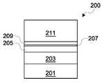
동작(101)을 수행한 후의 MRAM 구조물(200)의 일부분의 단면도인 도 2a를 참조한다. MRAM 구조물(200)은 기판(미도시됨)을 포함한다.2A, which is a cross-sectional view of a portion of the
도전성 플러그(미도시됨)가 기판 위의 유전체층(미도시됨)에 임베딩되면서 형성된다. 몇몇의 실시예들에서, 도전성 플러그는 알루미늄, 알루미늄 합금, 구리, 구리 합금, 티타늄, 티타늄 질화물, 탄탈륨, 탄탈륨 질화물, 텅스텐, 금속 실리사이드, 실리콘 또는 이들의 조합을 포함한다. 유전체층은 실리콘 산화물, FSG(fluorinated silica glass), 탄소 도핑된 실리콘 산화물, TEOS(tetra-ethyl-ortho-silicate) 산화물, PSG(phosphosilicate glass), BPSG(borophosphosilicate glass), 블랙 다이아몬드®(캘리포니아주 산타 클라라에 위치한 어플라이드 머터리얼스), 비정형 불소화 탄소, 로우 k 유전체 물질, 또는 이들의 조합을 포함한다. 몇몇의 실시예들에서, 형성 프로세스는 화학 기상 증착(chemical vapor deposition; CVD), 원자층 증착(atomic layer deposition; ALD), 고밀도 플라즈마 CVD(high density plasma CVD; HDPCVD) 또는 스핀 온 글래스(spin-on glass; SOG)를 포함한다.A conductive plug (not shown) is formed by being embedded in a dielectric layer (not shown) on the substrate. In some embodiments, the conductive plug comprises aluminum, an aluminum alloy, copper, a copper alloy, titanium, titanium nitride, tantalum, tantalum nitride, tungsten, metal silicide, silicon or combinations thereof. The dielectric layer is silicon oxide, FSG (fluorinated silica glass), carbon-doped silicon oxide, TEOS (tetra-ethyl-ortho -silicate) oxide, PSG (phosphosilicate glass), BPSG (borophosphosilicate glass), Black Diamond® (Santa Clara, California Lt; / RTI > materials), amorphous fluorinated carbon, low k dielectric materials, or combinations thereof. In some embodiments, the forming process is performed using chemical vapor deposition (CVD), atomic layer deposition (ALD), high density plasma CVD (HDPCVD), or spin- on glass (SOG).
바닥 전극 구조물(201)은 유전체층의 최상위 표면 위에 형성되고 도전성 플러그와 전기적으로 접촉한다. 바닥 전극 구조물(201)은 도전성 물질을 포함한다. 몇몇의 실시예들에서, 바닥 전극 구조물(201)은 티타늄(Ti), 탄탈륨(Ta), 백금(Pt), 루테늄(Ru), 텅스텐(W), 알루미늄(Al), 구리(Cu) 또는 이들의 조합을 포함한다. 바닥 전극 구조물(201)의 가능한 형성 방법들은 스퍼터링, PVD 또는 ALD를 포함한다. 몇몇의 실시예들에서, 바닥 전극 구조물(201)은 도전성 플러그를 통해, 트랜지스터와 같은, 아래에 위치한 전기적 컴포넌트에 전기적으로 연결된다.The
도 2a를 계속해서 참조하면, 반강자성 물질(anti-ferromagnetic material; AFM)층(203)이 바닥 전극 구조물(201) 위에 형성된다. 반강자성 물질(AFM)층(203)에서, 원자들(또는 분자들)의 자기 모멘트들은 규칙적인 패턴으로 이웃 원자들(또는 분자들)의 자기 모멘트들과 반대 방향으로 정렬된다. AFM 층(203)의 순 자기 모멘트는 제로(0)이다. 어떤 실시예들에서, AFM 층(203)은 백금 망간(PtMn)을 포함한다. 몇몇의 실시예들에서, AFM 층(203)은 이리듐 망간(IrMn), 로듐 망간(RhMn), 또는 철 망간(FeMn)을 포함한다. AFM 층(203)의 가능한 형성 방법들은 스퍼터링, PVD 또는 ALD를 포함한다. AFM 층(203)은 약 100Å 내지 약 200Å의 범위의 두께를 갖는다.2A, an anti-ferromagnetic material (AFM)
강자성 고정층(205)은 AFM 층(203) 위에 형성된다. 강자성 고정층(205)은 영구 자석을 형성하고 자석들과 강한 상호작용들을 나타낸다. 강자성 고정층(205)의 자기 모멘트의 방향은 인접한 AFM 층(203)에 의해 고정되고, MRAM 구조물(200)의 연계된 자기 터널 접합(MTJ) 엘리먼트의 동작 동안에 변경되지 않는다. 어떤 실시예들에서, 강자성 고정층(205)은 코발트 철 붕소(CoFeB)를 포함한다. 몇몇 실시예들에서, 강자성 고정층(205)은 CoFeTa, NiFe, Co, CoFe, CoPt, 또는 Ni, Co 및 Fe의 합금을 포함한다. 강자성 고정층(205)의 가능한 형성 방법들은 스퍼터링, PVD 또는 ALD를 포함한다. 적어도 하나의 실시예에서, 강자성 고정층(205)은 다층 구조물을 포함한다.A ferromagnetic pinned
터널링층(207)은 강자성 고정층(205) 위에 형성된다. 터널링층(207)은, 바이어싱 전압이 MRAM 구조물(200)에 인가될 때, 전자들이 터널링층을 터널링할 수 있도록 충분히 얇다. 어떤 실시예들에서, 터널링층(207)은 마그네슘 산화물(MgO), 알루미늄 산화물(Al2O3), 알루미늄 질화물(AlN), 알루미늄 산화질화물(AlON), 하프늄 산화물(HfO2) 또는 지르코늄 산화물(ZrO2)을 포함한다. 터널링층(207)은 약 5Å 내지 약 30Å의 범위의 두께를 갖는다. 터널링층(207)의 가능한 형성 방법들은 스퍼터링, PVD 또는 ALD를 포함한다.A
도 2a를 계속해서 참조하면, MRAM 구조물(200)은 터널링층(207) 위에 형성된 강자성 자유층(209)을 포함한다. 강자성 자유층(209)의 자기 모멘트의 방향은 고정되어 있지 않은데, 그 이유는 어떠한 반강자성 물질도 강자성 자유층(209)에 인접해 있지 않기 때문이다. 그러므로, 이 층의 자기 배향은 조정가능하며, 이에 따라 이 층을 자유층이라고 부른다. 적어도 하나의 실시예에서, 강자성 자유층(209)의 자기 모멘트의 방향은 강자성 고정층(205)의 자기 모멘트의 고정된 방향과 평행하거나 역평행해지도록 자유롭게 회전된다. 강자성 자유층(209)은 강자성 고정층(205)에서의 물질과 유사한 강자성 물질을 포함할 수 있다. 어떤 실시예들에서, 강자성 자유층(209)은 코발트, 니켈, 철, 또는 붕소를 포함한다. 강자성 자유층(209)의 가능한 형성 방법들은 스퍼터링, PVD 또는 ALD를 포함한다.2A, the
MRAM 구조물(200)은 강자성 자유층(209) 위에 형성된 최상단 전극층(211)을 포함한다. 최상단 전극층(211)은 도전성 물질을 포함한다. 몇몇의 실시예들에서, 최상단 전극층(211)은 조성의 관점에서 바닥 전극 구조물(201)과 유사하다. 몇몇의 실시예들에서, 최상단 전극층(211)은 티타늄(Ti), 탄탈륨(Ta), 백금(Pt), 루테늄(Ru), 텅스텐(W), 알루미늄(Al), 구리(Cu) 또는 이들의 조합을 포함한다. 최상단 전극층(211)은 전기적 라우팅을 위한 상호연결 구조물을 통해 MRAM 구조물(200)로부터 다른 부분들로의 전기적 연결을 제공한다.The
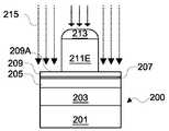
도 2b를 참조하면, 패터닝된 마스크층(213)이 최상단 전극층(211) 위에 형성된다. 어떤 실시예들에서, 패터닝된 마스크층(213)은 산화물, 질화물 또는 산화질화물과 같은 유전체 물질을 포함한다. 패터닝된 마스크층(213)은 퇴적, 리소그래피 패터닝, 및 에칭 프로세스들을 비롯한 적절한 프로세스에 의해 형성된다. 패터닝된 마스크층(213)은 최상단 전극 구조물을 정의하기 위한 에칭 마스크로서 이용된다.Referring to FIG. 2B, a patterned
도 1을 다시 참조하면, 방법(100)은 동작(102)으로 이어진다. 동작(102)에서, 최상단 전극층은 에칭되어 최상단 전극 구조물을 형성하고 강자성 자유층의 일부분을 노출시킨다.Referring back to FIG. 1, the
동작(102)을 수행한 후의 MRAM 구조물(200)의 일부분의 단면도인 도 2c를 참조한다. 최상단 전극 구조물(211E)을 정의하고 패터닝된 마스크층(213)에 의해 커버되지 않은 최상단 전극층(211)을 제거하기 위해 에칭 프로세스(215)가 수행된다. 에칭 프로세스(215)는 강자성 자유층(209)의 최상위 표면에서 중단될 수 있고, 에칭 프로세스(215) 이후 강자성 자유층(209)의 일부분은 노출이 된다. 최상단 전극 구조물(211E)은 측벽 표면들을 갖는다. 몇몇의 실시예들에서, 패터닝된 마스크층(213)의 일부분은 에칭 프로세스(215) 동안 소모되며, 이후의 프로세스들을 위해 나머지 패터닝된 마스크층(213)은 남겨진다.See FIG. 2C, which is a cross-sectional view of a portion of the
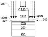
도 1을 다시 참조하면, 방법(100)은 동작(103)으로 이어진다. 동작(103)에서, 강자성 자유층의 노출된 부분을 탈자화(demagnetize)시키기 위한 처리가 수행된다.Referring back to FIG. 1, the
동작(103)을 수행한 후의 MRAM 구조물(200)의 일부분의 단면도인 도 2d를 참조한다. 처리(217)는 강자성 자유층의 노출된 부분(209T)에 수행된다. 처리(217)는 강자성 자유층의 노출된 부분(209T)을 탈자화시킨다. 최상단 전극 구조물(211E) 아래의 강자성 자유층의 부분(209N)은 처리(217)를 받지 않는다. 강자성 자유층의 부분(209N)은 강자성 고정층(205)의 제2 자기 모멘트의 방향에 대해 제1 자기 모멘트의 방향을 변경시키도록 구성가능하다. 강자성 자유층의 처리된 부분(209T)은 강자성 고정층(205)의 제2 자기 모멘트의 방향에 대해 제1 자기 모멘트의 방향을 변경시킬 수 없다.Reference is made to Fig. 2D, which is a cross-sectional view of a portion of the
어떤 실시예들에서, 처리(217)는 플라즈마 환경에서 수행된다. 몇몇의 실시예들에서, 플라즈마 환경은 산소 또는 질소와 같은 주요 가스를 포함한다. 플라즈마 환경의 동작 압력은 약 1 미리토르(mT) 내지 약 1000 mT의 범위에 있다. 이 압력 범위 밖에서는, 적절한 플라즈마 동작을 유지시키는 것은 어렵거나 또는, 몇몇의 경우들에서, 플라즈마는 점화될 수 없다. 분위기(ambience) 내에서의 산소 또는 질소의 주요 가스의 흐름은 약 5 sccm 내지 약 500 sccm의 범위에 있다. 몇몇의 실시예들에서, Ar, He 또는 Xe와 같은 캐리어 가스(또는 불활성 가스)가 첨가된다. 적어도 하나의 예시에서, 주요 가스의 흐름에 대한 캐리어 가스의 흐름의 비율은 약 80 내지 약 120의 범위에 있다. 이 흐름 범위 밖에서는, 강자성 자유층의 노출된 부분(209T)을 탈자화시키는 것은 어렵거나, 또는 몇몇의 경우들에서, 처리(217)는 최상단 전극 구조물(211E) 아래의 강자성 자유층의 부분(209N)의 일부분들을 횡측으로 손상시킬 것이다.In some embodiments, processing 217 is performed in a plasma environment. In some embodiments, the plasma environment comprises a main gas such as oxygen or nitrogen. The operating pressure of the plasma environment is in the range of about 1 millitorr (mT) to about 1000 mT. Outside this pressure range, it is difficult to maintain proper plasma operation or, in some cases, the plasma can not be ignited. The flow of oxygen or nitrogen gas in the ambience is in the range of about 5 sccm to about 500 sccm. In some embodiments, a carrier gas (or inert gas) such as Ar, He or Xe is added. In at least one example, the ratio of the flow of carrier gas to the flow of main gas is in the range of about 80 to about 120. Outside this flow range, it is difficult to demagnetize the exposed
몇몇의 실시예들에서, 처리(217)는 열 처리 프로세스에서 수행된다. 몇몇의 실시예들에서, 강자성 자유층의 처리된 부분(209T)은 코발트, 니켈, 철, 붕소, 산소 또는 질소를 포함한다.In some embodiments, processing 217 is performed in a thermal processing process. In some embodiments, the treated
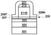
도 1을 다시 참조하면, 방법(100)은 동작(104)으로 이어진다. 동작(104)에서, 보호층이 최상단 전극 구조물 및 강자성 자유층의 처리된 부분 위에 형성된다.Referring again to FIG. 1, the
동작(104)을 수행한 후의 MRAM 구조물(200)의 일부분의 단면도인 도 2e를 참조한다. 보호층(221)은 패터닝된 마스크층(213), 최상단 전극 구조물(211E)의 측벽 표면들, 및 강자성 자유층의 처리된 부분(209T) 위에 블랭킷 퇴적(blanket deposited)된다. 보호층(221)은 실리콘 산화물, 실리콘 질화물, 실리콘 산화질화물 또는 로우 k 유전체와 같은 적어도 하나의 유전체 물질을 포함한다. 보호층(221)의 가능한 형성 방법들은 CVD, SOG 또는 ALD를 포함한다.See FIG. 2E, which is a cross-sectional view of a portion of the
도 1을 다시 참조하면, 방법(100)은 동작들(105, 106)으로 이어진다. 동작(105)에서, 보호층은 에칭되어 최상단 전극 구조물의 측벽 표면들 및 강자성 자유층의 처리된 부분의 일부분 위에 보호 스페이서들을 형성한다. 동작(106)에서, 강자성 자유층의 처리된 부분, 터널링층, 고정층 및 반강자성 물질층은 에칭되어 자기 터널 접합 엘리먼트를 형성한다. 몇몇의 실시예들에서, 동작들(105, 106) 사이에서 자기 터널 접합 엘리먼트를 공기와 같은 외부 환경에 노출시키지 않는 상이한 프로세스 쳄버들을 갖는 동일한 어셈블리에서 동작들(105, 106)이 수행된다.Referring back to Figure 1, the
동작들(105, 106)을 수행한 후의 MRAM 구조물(200)의 일부분의 단면도인 도 2f를 참조한다. 보호층(221)을 에칭하고 강자성 자유층의 처리된 부분(209T) 위의 보호층(221)의 대부분을 제거하기 위해 에칭 프로세스(미도시됨)가 수행된다. 보호 스페이서들(221S)은 최상단 전극 구조물(211E)의 측벽 표면들 및 강자성 자유층의 처리된 부분(209T)의 일부분 위에 형성된다. 몇몇의 실시예들에서, 패터닝된 마스크층(213)은 이 에칭 프로세스에서 소모되며, 최상단 전극 구조물(211E)의 최상위 표면은 노출된다.Reference is made to Figure 2f, which is a cross-sectional view of a portion of the
동작(106)을 수행한 후의 MRAM 구조물(200)의 일부분의 단면도인 도 2f를 계속해서 참조한다. 강자성 자유층의 처리된 부분(209T), 터널링층(207), 강자성 고정층(205) 및 AFM 층(203)을 에칭하여 자기 터널 접합(MTJ) 엘리먼트(250)를 형성하기 위해 에칭 프로세스(223)가 수행된다. 몇몇의 실시예들에서, 에칭 프로세스(223)는 플라즈마 환경에서 수행된다. 보호 스페이서들(221S) 및 최상단 전극 구조물(211E)에 의해 커버되지 않는 층들(209, 207, 205, 203)의 부분들은 제거된다. MTJ 엘리먼트(250A)를 형성하기 위해 보호 스페이서들(221S)은 에칭 마스크로서 이용되며, 보호 스페이서들(221S)의 측벽 표면은 MTJ 엘리먼트(250)의 측벽 표면과 실질적으로 정렬된다. MTJ 엘리먼트(250)는 AFM 층(203), 강자성 고정층(205), 터널링층(207), 최상단 전극 구조물(211E) 아래에 있는 강자성 자유층의 부분(209N)(이것을 또한 기능부(209N)라고 칭한다), 및 강자성 자유층의 처리된 부분(209T)(이것을 또한 비기능부(209T)라고 칭한다)을 포함한다. 강자성 자유층의 비기능부(209T)는 최상단 전극 구조물(211E)의 가장자리를 넘어 연장한다.Continue reference to Figure 2f, which is a cross-sectional view of a portion of the
유리하게도, 강자성 자유층의 기능부(209N)는, 비기능부(209T)에 의해 둘러싸여지며, MTJ 엘리먼트(250)의 형성 동안에 플라즈마 환경으로부터 격리된다. 몇몇의 실시예들에서, MTJ 엘리먼트(250) 형성을 위한 에칭 프로세스(223)에서의 플라즈마 공격으로 인해 기능부(209N)의 자기 특성들은 저하되지 않는다. 기능부(209N)의 자기 특성들을 유지하기 때문에 MRAM 구조물(200)에 대한 전기 특성 안정성은 증대된다.Advantageously, the functioning
도 2g는 동작(106)을 수행한 후에 택일적 사항으로서 형성된 MRAM 구조물(200)의 단면도이다. MRAM 구조물(200)은 유전체층(225) 및 바닥 전극 구조물(201) 아래에 있는 도전성 플러그(229A)를 더 포함한다. 금속간 유전체(inter-metal dielectric; IMD)층(227)이 도 2g에서 도시된 바와 같이, MRAM 구조물(200) 위에 형성된다. 몇몇의 실시예들에서, IMD층(227)은 MRAM 구조물(200)을 둘러싼다. IMD층(227)을 평탄화시키기 위해 MRAM 구조물(200)에 화학 기계적 폴리싱(chemical mechanical polishing; CMP) 프로세스가 추가로 적용된다. 몇몇의 실시예들에서, IMD층(227)은 다중 유전체층들을 포함한다. 몇몇의 실시예들에서, IMD층(227)은 실리콘 산화물, FSG(fluorinated silica glass), 탄소 도핑된 실리콘 산화물, TEOS(tetra-ethyl-ortho-silicate) 산화물, PSG(phosphosilicate glass), BPSG(borophosphosilicate glass), 블랙 다이아몬드®(캘리포니아주 산타 클라라에 위치한 어플라이드 머터리얼스), 비정형 불소화 탄소, 로우 k 유전체 물질, 또는 이들의 조합을 포함한다.FIG. 2G is a cross-sectional view of the
어떤 실시예들에서, 최상단 전극 구조물(211E)과 전기적으로 접촉하는 도전성 와이어(231) 및 도전성 플러그(229B)를 형성하기 위해, 듀얼 다마신 프로세스가 IMD 층(227)에서 수행된다. 도전성 와이어(231) 및 도전성 플러그(229B)의 도전성 물질에는 구리, 구리 합금, 알루미늄 또는 텅스텐이 포함된다.In some embodiments, a dual damascene process is performed on the
본 실시예들 및 이들의 장점들을 자세하게 설명하였지만, 여기에 다양한 변경, 대체, 및 변동이 첨부된 청구범위들에 의해 정의된 본 실시예들의 범위 및 사상을 벗어나지 않고서 행해질 수 있다는 것을 이해해야 한다. 본 발명분야의 당업자라면 여기서 설명된 대응하는 실시예들과 실질적으로 동일한 기능을 수행하거나 또는 이와 실질적으로 동일한 결과를 달성하는 물질, 수단, 방법, 또는 단계의 공정, 머신, 제조, 조성이 본 발명개시에 따라 이용될 수 있다는 것을 본 발명개시로부터 손쉽게 알 것이다. 따라서, 첨부된 청구항들은 이와 같은 물질, 수단, 방법, 또는 단계의 공정, 머신, 제조, 조성을 청구항의 범위내에 포함하는 것으로 한다.Although the embodiments and their advantages have been described in detail, it should be understood that various changes, substitutions, and alterations can be made herein without departing from the scope and spirit of the embodiments, which is defined by the appended claims. It will be apparent to those skilled in the art that the process, machine, manufacture, and composition of a material, means, method, or step that performs substantially the same function or achieve substantially the same result as the corresponding embodiments described herein, It will be readily appreciated from the disclosure of the present invention that it can be used according to the disclosure. Accordingly, the appended claims are intended to cover within the scope of the claims the process, machine, manufacture, composition of such material, means, method, or step.
Claims (10)
Translated fromKorean바닥 전극 구조물;
상기 바닥 전극 구조물 위의 자기 터널 접합(magnetic tunnel junction; MTJ) 엘리먼트로서, 상기 MTJ 엘리먼트는,
상기 바닥 전극 구조물 위의 반강자성 물질(anti-ferromagnetic material; AFM)층;
상기 반강자성 물질층 위의 강자성 고정층;
상기 강자성 고정층 위의 터널링층; 및
제1 부분 및 탈자화된(demagnetized) 제2 부분을 가지며, 상기 터널링층 위에 있는 강자성 자유층을 포함하는 것인, 상기 MTJ 엘리먼트; 및
상기 제1 부분 위의 제1 너비를 갖는 최상단 전극으로서, 상기 최상단 전극은 측벽들 및 상기 측벽들의 하부 부분 위의 보호 스페이서들을 포함하고, 상기 보호 스페이서들은 상기 강자성 자유층의 탈자화된 제2 부분 위에 놓이며 상기 최상단 전극의 최상단 표면을 노출시키고, 상기 보호 스페이서들 중 적어도 하나는 상기 탈자화된 제2 부분과 정렬되고 상기 탈자화된 제2 부분으로부터 상기 최상단 전극으로 연장하는 곡면 표면을 갖는 것인, 상기 최상단 전극
을 포함하고,
상기 최상단 전극의 측벽들의 일부분은 상기 보호 스페이서들의 최상단 표면 위에 있는 것인, 자기저항 랜덤 액세스 메모리(MRAM) 구조물.In a magnetoresistive random access memory (MRAM) structure,
Bottom electrode structure;
A magnetic tunnel junction (MTJ) element on the bottom electrode structure, the MTJ element comprising:
An anti-ferromagnetic material (AFM) layer on the bottom electrode structure;
A ferromagnetic pinned layer on the antiferromagnetic material layer;
A tunneling layer on the ferromagnetic pinned layer; And
The MTJ element having a first portion and a demagnetized second portion, the ferromagnetic free layer being on the tunneling layer; And
A top electrode having a first width over the first portion, the top electrode comprising protective sockets on sidewalls and a bottom portion of the sidewalls, and wherein the protective spacers are formed on the denitrified second portion of the ferromagnetic free layer And at least one of the protective spacers having a curved surface that is aligned with the demagnetized second portion and extends from the demagnetized second portion to the uppermost electrode The uppermost electrode
/ RTI >
And a portion of the sidewalls of the uppermost electrode is on the uppermost surface of the protection spacers.
바닥 전극 구조물;
상기 바닥 전극 구조물 위의 자기 터널 접합(magnetic tunnel junction; MTJ) 엘리먼트로서, 상기 MTJ 엘리먼트는,
상기 바닥 전극 구조물 위의 반강자성 물질층;
상기 반강자성 물질층 위의 강자성 고정층;
상기 강자성 고정층 위의 터널링층; 및
제1 부분 및 탈자화된 제2 부분을 가지며, 상기 터널링층 위에 있는 강자성 자유층을 포함하는 것인, 상기 MTJ 엘리먼트; 및
측벽 표면들을 가지며, 상기 강자성 자유층의 제1 부분 위에 있는 최상단 전극 구조물; 및
상기 최상단 전극 구조물의 측벽 표면들 위 및 상기 강자성 자유층의 탈자화된 제2 부분 위의 보호 스페이서들
을 포함하고,
상기 보호 스페이서들 중 적어도 하나는 상기 강자성 자유층의 탈자화된 제2 부분의 적어도 두 개의 측벽들과 정렬되고, 상기 최상단 전극 구조물의 측벽들의 일부분은 상기 보호 스페이서들의 최상단 곡면 표면 위에 있는 것인, 자기저항 랜덤 액세스 메모리(MRAM) 구조물.In a magnetoresistive random access memory (MRAM) structure,
Bottom electrode structure;
A magnetic tunnel junction (MTJ) element on the bottom electrode structure, the MTJ element comprising:
An antiferromagnetic material layer on the bottom electrode structure;
A ferromagnetic pinned layer on the antiferromagnetic material layer;
A tunneling layer on the ferromagnetic pinned layer; And
The MTJ element having a first portion and a demagnetized second portion, the ferromagnetic free layer being on the tunneling layer; And
A top electrode structure having sidewall surfaces, said top electrode structure overlying a first portion of said ferromagnetic free layer; And
The protective spacers on the sidewall surfaces of the uppermost electrode structure and on the desquaminated second portion of the ferromagnetic free layer
/ RTI >
Wherein at least one of the protective spacers is aligned with at least two sidewalls of the desquaminated second portion of the ferromagnetic free layer and a portion of the sidewalls of the top electrode structure is above the top curved surface of the protective spacers. Magnetoresistive random access memory (MRAM) structures.
반강자성 물질층, 상기 반강자성 물질층 위의 고정층, 상기 고정층 위의 터널링층, 상기 터널링층 위의 강자성 자유층, 및 상기 강자성 자유층 위의 최상단 전극층을 제공하는 단계;
상기 최상단 전극층을 에칭하여 최상단 전극 구조물을 형성하고 상기 강자성 자유층의 일부분을 노출시키는 단계;
상기 강자성 자유층의 노출된 부분에 탈자화를 수행하는 단계;
상기 최상단 전극 구조물 및 상기 강자성 자유층의 탈자화된 부분 위에 보호층을 형성하는 단계;
상기 최상단 전극 구조물의 측벽들의 일부분이 보호 스페이서들의 상단 표면 위에 있도록, 상기 보호층을 에칭하여 상기 최상단 전극 구조물의 하부 측벽 표면들 및 상기 강자성 자유층의 탈자화된 부분의 일부분 위에 상기 보호 스페이서들을 형성하는 단계; 및
상기 강자성 자유층의 탈자화된 부분, 상기 터널링층, 상기 고정층 및 상기 반강자성 물질층을 에칭하여 자기 터널 접합 엘리먼트를 형성하는 단계
를 포함하고,
상기 보호 스페이서들 중 적어도 하나는 상기 탈자화된 부분과 정렬되고 상기 탈자화된 부분으로부터 상기 최상단 전극 구조물로 연장하는 곡면 표면을 갖는 것인, 자기저항 랜덤 액세스 메모리(MRAM) 구조물을 형성하는 방법.A method of forming a magnetoresistive random access memory (MRAM) structure,
Providing an antiferromagnetic material layer, a pinning layer over the antiferromagnetic material layer, a tunneling layer over the pinning layer, a ferromagnetic free layer over the tunneling layer, and a top electrode layer over the ferromagnetic free layer.
Etching the top electrode layer to form a top electrode structure and exposing a portion of the ferromagnetic free layer;
Performing demagnetization on an exposed portion of the ferromagnetic free layer;
Forming a protective layer on the uppermost electrode structure and the desized portion of the ferromagnetic free layer;
Etching the passivation layer such that a portion of the sidewalls of the top electrode structure is on the top surface of the protective spacers to form the protective spacers on portions of the bottom sidewall surfaces of the top electrode structure and the desized portion of the ferromagnetic free layer ; And
Etching the demagnetized portion of the ferromagnetic free layer, the tunneling layer, the pinned layer and the antiferromagnetic material layer to form a magnetic tunnel junction element
Lt; / RTI >
Wherein at least one of the protective spacers has a curved surface that is aligned with the demagnetized portion and extends from the demagnetized portion to the top electrode structure. ≪ Desc / Clms Page number 13 >
Applications Claiming Priority (2)
| Application Number | Priority Date | Filing Date | Title |
|---|---|---|---|
| US13/945,534 | 2013-07-18 | ||
| US13/945,534US9595661B2 (en) | 2013-07-18 | 2013-07-18 | Magnetoresistive random access memory structure and method of forming the same |
Publications (2)
| Publication Number | Publication Date |
|---|---|
| KR20150010600A KR20150010600A (en) | 2015-01-28 |
| KR101669720B1true KR101669720B1 (en) | 2016-10-27 |
Family
ID=52319733
Family Applications (1)
| Application Number | Title | Priority Date | Filing Date |
|---|---|---|---|
| KR1020140086227AActiveKR101669720B1 (en) | 2013-07-18 | 2014-07-09 | Magnetoresistive random access memory structure and method of forming the same |
Country Status (3)
| Country | Link |
|---|---|
| US (3) | US9595661B2 (en) |
| KR (1) | KR101669720B1 (en) |
| CN (2) | CN104300080A (en) |
Families Citing this family (20)
| Publication number | Priority date | Publication date | Assignee | Title |
|---|---|---|---|---|
| US9257636B2 (en) | 2013-09-11 | 2016-02-09 | Taiwan Semiconductor Manufacturing Co., Ltd. | Perpendicular magnetic random-access memory (MRAM) formation by direct self-assembly method |
| US9559294B2 (en) | 2015-01-29 | 2017-01-31 | Taiwan Semiconductor Manufacturing Co., Ltd. | Self-aligned magnetoresistive random-access memory (MRAM) structure for process damage minimization |
| US10008662B2 (en) | 2015-03-12 | 2018-06-26 | Taiwan Semiconductor Manufacturing Co., Ltd. | Perpendicular magnetic tunneling junction (MTJ) for improved magnetoresistive random-access memory (MRAM) process |
| US9472753B1 (en) | 2015-06-02 | 2016-10-18 | HGST Netherlands B.V. | Method for fabricating MRAM bits on a tight pitch |
| KR102444236B1 (en) | 2015-08-25 | 2022-09-16 | 삼성전자주식회사 | Magnetic element and manufacturing method thereof |
| KR102473663B1 (en) | 2015-10-01 | 2022-12-02 | 삼성전자주식회사 | Semiconductor device having a magnetic tunnel junction assembly and Method for fabricating the same |
| ES2877374T3 (en)* | 2015-12-15 | 2021-11-16 | Air Liquide | Apparatus for endothermic processes with improved burner arrangement |
| GB2561790B (en)* | 2016-02-01 | 2021-05-12 | Canon Anelva Corp | Manufacturing method of magneto-resistive effect device |
| US9917137B1 (en) | 2017-01-11 | 2018-03-13 | International Business Machines Corporation | Integrated magnetic tunnel junction (MTJ) in back end of line (BEOL) interconnects |
| KR102368033B1 (en) | 2017-09-20 | 2022-02-25 | 삼성전자주식회사 | Method of manufacturing a magnetoresistive random access device |
| KR102372829B1 (en)* | 2017-09-27 | 2022-03-10 | 삼성전자주식회사 | Magnetoresistive random access memory device |
| US10741748B2 (en) | 2018-06-25 | 2020-08-11 | International Business Machines Corporation | Back end of line metallization structures |
| CN112599557B (en)* | 2018-07-19 | 2023-09-12 | 联华电子股份有限公司 | Magnetic random access memory structure |
| US11043251B2 (en) | 2018-11-30 | 2021-06-22 | Taiwan Semiconductor Manufacturing Company, Ltd. | Magnetic tunnel junction device and method of forming same |
| CN111435702B (en)* | 2019-01-14 | 2023-05-19 | 联华电子股份有限公司 | Magnetoresistive random access memory cell |
| US10944044B2 (en) | 2019-08-07 | 2021-03-09 | International Business Machines Corporation | MRAM structure with T-shaped bottom electrode to overcome galvanic effect |
| TWI815948B (en) | 2019-08-14 | 2023-09-21 | 聯華電子股份有限公司 | Semiconductor device and method for fabricating the same |
| CN112563412B (en)* | 2019-09-25 | 2023-06-23 | 浙江驰拓科技有限公司 | Magnetic tunnel junction etching method |
| CN114156404A (en)* | 2021-11-09 | 2022-03-08 | 中电海康集团有限公司 | Magnetic tunnel junction with high overturning efficiency and preparation method thereof |
| US20230389331A1 (en)* | 2022-05-26 | 2023-11-30 | Taiwan Semiconductor Manufacturing Company, Ltd. | Memory cell isolation |
Citations (3)
| Publication number | Priority date | Publication date | Assignee | Title |
|---|---|---|---|---|
| JP2001160640A (en) | 1999-09-24 | 2001-06-12 | Toshiba Corp | Magnetoresistive element, magnetoresistive head, magnetic reproducing device, and magnetic laminate |
| US20050277206A1 (en) | 2004-06-11 | 2005-12-15 | International Business Machines Corporation | Structure and method of patterning a magnetic tunnel junction stack for a magneto-resistive random access memory |
| JP5117421B2 (en) | 2009-02-12 | 2013-01-16 | 株式会社東芝 | Magnetoresistive element and manufacturing method thereof |
Family Cites Families (18)
| Publication number | Priority date | Publication date | Assignee | Title |
|---|---|---|---|---|
| KR100373473B1 (en) | 1999-09-24 | 2003-02-25 | 가부시끼가이샤 도시바 | Magnetoresistance device, magnetoresistance head, magnetoreproducing device, and magnetic stacked body |
| US6680832B2 (en)* | 2001-05-11 | 2004-01-20 | International Business Machines Corporation | CPP magnetoresistive sensors with in-stack longitudinal biasing and overlapping magnetic shield |
| US6759263B2 (en)* | 2002-08-29 | 2004-07-06 | Chentsau Ying | Method of patterning a layer of magnetic material |
| JP2004288984A (en) | 2003-03-24 | 2004-10-14 | Sharp Corp | Film forming apparatus and film forming method |
| KR100500455B1 (en)* | 2003-08-11 | 2005-07-18 | 삼성전자주식회사 | Magnetic tunnel junction structure having a oxidized buffer layer and method of fabricating the same |
| EP1667160B1 (en)* | 2004-12-03 | 2011-11-23 | Samsung Electronics Co., Ltd. | Magnetic memory device and method |
| US7531367B2 (en)* | 2006-01-18 | 2009-05-12 | International Business Machines Corporation | Utilizing sidewall spacer features to form magnetic tunnel junctions in an integrated circuit |
| US20070187785A1 (en)* | 2006-02-16 | 2007-08-16 | Chien-Chung Hung | Magnetic memory cell and manufacturing method thereof |
| US20080044984A1 (en)* | 2006-08-16 | 2008-02-21 | Taiwan Semiconductor Manufacturing Co., Ltd. | Methods of avoiding wafer breakage during manufacture of backside illuminated image sensors |
| JP5107128B2 (en)* | 2008-04-23 | 2012-12-26 | ルネサスエレクトロニクス株式会社 | Manufacturing method of semiconductor device |
| US9368716B2 (en)* | 2009-02-02 | 2016-06-14 | Qualcomm Incorporated | Magnetic tunnel junction (MTJ) storage element and spin transfer torque magnetoresistive random access memory (STT-MRAM) cells having an MTJ |
| US7989224B2 (en)* | 2009-04-30 | 2011-08-02 | International Business Machines Corporation | Sidewall coating for non-uniform spin momentum-transfer magnetic tunnel junction current flow |
| US8981502B2 (en)* | 2010-03-29 | 2015-03-17 | Qualcomm Incorporated | Fabricating a magnetic tunnel junction storage element |
| KR101746615B1 (en)* | 2010-07-22 | 2017-06-14 | 삼성전자 주식회사 | Magnetic memory device and memory card and system including the same |
| US8709956B2 (en)* | 2011-08-01 | 2014-04-29 | Avalanche Technology Inc. | MRAM with sidewall protection and method of fabrication |
| US8796795B2 (en)* | 2011-08-01 | 2014-08-05 | Avalanche Technology Inc. | MRAM with sidewall protection and method of fabrication |
| CN103066199B (en)* | 2011-10-19 | 2016-03-30 | 中芯国际集成电路制造(北京)有限公司 | A kind of novel magnetic tunnel junction device and manufacture method thereof |
| US8772888B2 (en)* | 2012-08-10 | 2014-07-08 | Avalanche Technology Inc. | MTJ MRAM with stud patterning |
- 2013
- 2013-07-18USUS13/945,534patent/US9595661B2/enactiveActive
- 2013-09-30CNCN201310462757.8Apatent/CN104300080A/enactivePending
- 2013-09-30CNCN201910089450.5Apatent/CN110010757A/enactivePending
- 2014
- 2014-07-09KRKR1020140086227Apatent/KR101669720B1/enactiveActive
- 2017
- 2017-03-10USUS15/455,720patent/US10181558B2/enactiveActive
- 2018
- 2018-12-28USUS16/235,816patent/US10937956B2/enactiveActive
Patent Citations (3)
| Publication number | Priority date | Publication date | Assignee | Title |
|---|---|---|---|---|
| JP2001160640A (en) | 1999-09-24 | 2001-06-12 | Toshiba Corp | Magnetoresistive element, magnetoresistive head, magnetic reproducing device, and magnetic laminate |
| US20050277206A1 (en) | 2004-06-11 | 2005-12-15 | International Business Machines Corporation | Structure and method of patterning a magnetic tunnel junction stack for a magneto-resistive random access memory |
| JP5117421B2 (en) | 2009-02-12 | 2013-01-16 | 株式会社東芝 | Magnetoresistive element and manufacturing method thereof |
Also Published As
| Publication number | Publication date |
|---|---|
| KR20150010600A (en) | 2015-01-28 |
| US10937956B2 (en) | 2021-03-02 |
| US20150021725A1 (en) | 2015-01-22 |
| US9595661B2 (en) | 2017-03-14 |
| US20170186946A1 (en) | 2017-06-29 |
| US10181558B2 (en) | 2019-01-15 |
| US20190140169A1 (en) | 2019-05-09 |
| CN104300080A (en) | 2015-01-21 |
| CN110010757A (en) | 2019-07-12 |
Similar Documents
| Publication | Publication Date | Title |
|---|---|---|
| US10937956B2 (en) | Magnetoresistive random access memory structure and method of forming the same | |
| US12219880B2 (en) | Integrated circuit device | |
| US11063217B2 (en) | Semiconductor device | |
| US11355701B2 (en) | Integrated circuit | |
| US9991440B2 (en) | Magnetoresistive random access memory cell and fabricating the same | |
| US11171284B2 (en) | Memory device | |
| TW201639121A (en) | Magneto-resistive random-access memory and method for forming the same | |
| KR102354657B1 (en) | Sot mram having dielectric interfacial layer and method forming same | |
| US11189791B2 (en) | Integrated circuit and fabrication method thereof | |
| CN109994600B (en) | Method for manufacturing magnetic random access memory | |
| US12048250B2 (en) | Method of fabricating magneto-resistive random access memory (MRAM) | |
| US12250826B2 (en) | Integrated circuit device and method for fabricating the same |
Legal Events
| Date | Code | Title | Description |
|---|---|---|---|
| A201 | Request for examination | ||
| PA0109 | Patent application | St.27 status event code:A-0-1-A10-A12-nap-PA0109 | |
| PA0201 | Request for examination | St.27 status event code:A-1-2-D10-D11-exm-PA0201 | |
| D13-X000 | Search requested | St.27 status event code:A-1-2-D10-D13-srh-X000 | |
| PG1501 | Laying open of application | St.27 status event code:A-1-1-Q10-Q12-nap-PG1501 | |
| R17-X000 | Change to representative recorded | St.27 status event code:A-3-3-R10-R17-oth-X000 | |
| D14-X000 | Search report completed | St.27 status event code:A-1-2-D10-D14-srh-X000 | |
| R18-X000 | Changes to party contact information recorded | St.27 status event code:A-3-3-R10-R18-oth-X000 | |
| E902 | Notification of reason for refusal | ||
| PE0902 | Notice of grounds for rejection | St.27 status event code:A-1-2-D10-D21-exm-PE0902 | |
| T11-X000 | Administrative time limit extension requested | St.27 status event code:U-3-3-T10-T11-oth-X000 | |
| AMND | Amendment | ||
| P11-X000 | Amendment of application requested | St.27 status event code:A-2-2-P10-P11-nap-X000 | |
| P13-X000 | Application amended | St.27 status event code:A-2-2-P10-P13-nap-X000 | |
| E601 | Decision to refuse application | ||
| PE0601 | Decision on rejection of patent | St.27 status event code:N-2-6-B10-B15-exm-PE0601 | |
| AMND | Amendment | ||
| P11-X000 | Amendment of application requested | St.27 status event code:A-2-2-P10-P11-nap-X000 | |
| P13-X000 | Application amended | St.27 status event code:A-2-2-P10-P13-nap-X000 | |
| PX0901 | Re-examination | St.27 status event code:A-2-3-E10-E12-rex-PX0901 | |
| PX0701 | Decision of registration after re-examination | St.27 status event code:A-3-4-F10-F13-rex-PX0701 | |
| X701 | Decision to grant (after re-examination) | ||
| GRNT | Written decision to grant | ||
| PR0701 | Registration of establishment | St.27 status event code:A-2-4-F10-F11-exm-PR0701 | |
| PR1002 | Payment of registration fee | St.27 status event code:A-2-2-U10-U11-oth-PR1002 Fee payment year number:1 | |
| PG1601 | Publication of registration | St.27 status event code:A-4-4-Q10-Q13-nap-PG1601 | |
| R18-X000 | Changes to party contact information recorded | St.27 status event code:A-5-5-R10-R18-oth-X000 | |
| FPAY | Annual fee payment | Payment date:20191010 Year of fee payment:4 | |
| PR1001 | Payment of annual fee | St.27 status event code:A-4-4-U10-U11-oth-PR1001 Fee payment year number:4 | |
| PR1001 | Payment of annual fee | St.27 status event code:A-4-4-U10-U11-oth-PR1001 Fee payment year number:5 | |
| PR1001 | Payment of annual fee | St.27 status event code:A-4-4-U10-U11-oth-PR1001 Fee payment year number:6 | |
| PR1001 | Payment of annual fee | St.27 status event code:A-4-4-U10-U11-oth-PR1001 Fee payment year number:7 | |
| P22-X000 | Classification modified | St.27 status event code:A-4-4-P10-P22-nap-X000 | |
| P22-X000 | Classification modified | St.27 status event code:A-4-4-P10-P22-nap-X000 | |
| PR1001 | Payment of annual fee | St.27 status event code:A-4-4-U10-U11-oth-PR1001 Fee payment year number:8 | |
| PR1001 | Payment of annual fee | St.27 status event code:A-4-4-U10-U11-oth-PR1001 Fee payment year number:9 | |
| PR1001 | Payment of annual fee | St.27 status event code:A-4-4-U10-U11-oth-PR1001 Fee payment year number:10 |