KR101667656B1 - Method of forming package on package - Google Patents
Method of forming package on packageDownload PDFInfo
- Publication number
- KR101667656B1 KR101667656B1KR1020100026393AKR20100026393AKR101667656B1KR 101667656 B1KR101667656 B1KR 101667656B1KR 1020100026393 AKR1020100026393 AKR 1020100026393AKR 20100026393 AKR20100026393 AKR 20100026393AKR 101667656 B1KR101667656 B1KR 101667656B1
- Authority
- KR
- South Korea
- Prior art keywords
- package
- semiconductor
- wafer
- penetrating electrodes
- connection terminals
- Prior art date
- Legal status (The legal status is an assumption and is not a legal conclusion. Google has not performed a legal analysis and makes no representation as to the accuracy of the status listed.)
- Active
Links
Images


Classifications
- H—ELECTRICITY
- H01—ELECTRIC ELEMENTS
- H01L—SEMICONDUCTOR DEVICES NOT COVERED BY CLASS H10
- H01L23/00—Details of semiconductor or other solid state devices
- H01L23/52—Arrangements for conducting electric current within the device in operation from one component to another, i.e. interconnections, e.g. wires, lead frames
- H01L23/522—Arrangements for conducting electric current within the device in operation from one component to another, i.e. interconnections, e.g. wires, lead frames including external interconnections consisting of a multilayer structure of conductive and insulating layers inseparably formed on the semiconductor body
- H01L23/5226—Via connections in a multilevel interconnection structure
- H—ELECTRICITY
- H01—ELECTRIC ELEMENTS
- H01L—SEMICONDUCTOR DEVICES NOT COVERED BY CLASS H10
- H01L25/00—Assemblies consisting of a plurality of semiconductor or other solid state devices
- H01L25/03—Assemblies consisting of a plurality of semiconductor or other solid state devices all the devices being of a type provided for in a single subclass of subclasses H10B, H10D, H10F, H10H, H10K or H10N, e.g. assemblies of rectifier diodes
- H01L25/10—Assemblies consisting of a plurality of semiconductor or other solid state devices all the devices being of a type provided for in a single subclass of subclasses H10B, H10D, H10F, H10H, H10K or H10N, e.g. assemblies of rectifier diodes the devices having separate containers
- H01L25/105—Assemblies consisting of a plurality of semiconductor or other solid state devices all the devices being of a type provided for in a single subclass of subclasses H10B, H10D, H10F, H10H, H10K or H10N, e.g. assemblies of rectifier diodes the devices having separate containers the devices being integrated devices of class H10
- H—ELECTRICITY
- H01—ELECTRIC ELEMENTS
- H01L—SEMICONDUCTOR DEVICES NOT COVERED BY CLASS H10
- H01L21/00—Processes or apparatus adapted for the manufacture or treatment of semiconductor or solid state devices or of parts thereof
- H01L21/70—Manufacture or treatment of devices consisting of a plurality of solid state components formed in or on a common substrate or of parts thereof; Manufacture of integrated circuit devices or of parts thereof
- H01L21/77—Manufacture or treatment of devices consisting of a plurality of solid state components or integrated circuits formed in, or on, a common substrate
- H01L21/78—Manufacture or treatment of devices consisting of a plurality of solid state components or integrated circuits formed in, or on, a common substrate with subsequent division of the substrate into plural individual devices
- H—ELECTRICITY
- H01—ELECTRIC ELEMENTS
- H01L—SEMICONDUCTOR DEVICES NOT COVERED BY CLASS H10
- H01L23/00—Details of semiconductor or other solid state devices
- H01L23/48—Arrangements for conducting electric current to or from the solid state body in operation, e.g. leads, terminal arrangements ; Selection of materials therefor
- H01L23/481—Internal lead connections, e.g. via connections, feedthrough structures
- H—ELECTRICITY
- H01—ELECTRIC ELEMENTS
- H01L—SEMICONDUCTOR DEVICES NOT COVERED BY CLASS H10
- H01L24/00—Arrangements for connecting or disconnecting semiconductor or solid-state bodies; Methods or apparatus related thereto
- H01L24/80—Methods for connecting semiconductor or other solid state bodies using means for bonding being attached to, or being formed on, the surface to be connected
- H01L24/81—Methods for connecting semiconductor or other solid state bodies using means for bonding being attached to, or being formed on, the surface to be connected using a bump connector
- H—ELECTRICITY
- H01—ELECTRIC ELEMENTS
- H01L—SEMICONDUCTOR DEVICES NOT COVERED BY CLASS H10
- H01L25/00—Assemblies consisting of a plurality of semiconductor or other solid state devices
- H01L25/03—Assemblies consisting of a plurality of semiconductor or other solid state devices all the devices being of a type provided for in a single subclass of subclasses H10B, H10D, H10F, H10H, H10K or H10N, e.g. assemblies of rectifier diodes
- H01L25/04—Assemblies consisting of a plurality of semiconductor or other solid state devices all the devices being of a type provided for in a single subclass of subclasses H10B, H10D, H10F, H10H, H10K or H10N, e.g. assemblies of rectifier diodes the devices not having separate containers
- H01L25/065—Assemblies consisting of a plurality of semiconductor or other solid state devices all the devices being of a type provided for in a single subclass of subclasses H10B, H10D, H10F, H10H, H10K or H10N, e.g. assemblies of rectifier diodes the devices not having separate containers the devices being of a type provided for in group H10D89/00
- H01L25/0657—Stacked arrangements of devices
- H—ELECTRICITY
- H01—ELECTRIC ELEMENTS
- H01L—SEMICONDUCTOR DEVICES NOT COVERED BY CLASS H10
- H01L25/00—Assemblies consisting of a plurality of semiconductor or other solid state devices
- H01L25/16—Assemblies consisting of a plurality of semiconductor or other solid state devices the devices being of types provided for in two or more different subclasses of H10B, H10D, H10F, H10H, H10K or H10N, e.g. forming hybrid circuits
- H—ELECTRICITY
- H01—ELECTRIC ELEMENTS
- H01L—SEMICONDUCTOR DEVICES NOT COVERED BY CLASS H10
- H01L25/00—Assemblies consisting of a plurality of semiconductor or other solid state devices
- H01L25/50—Multistep manufacturing processes of assemblies consisting of devices, the devices being individual devices of subclass H10D or integrated devices of class H10
- H—ELECTRICITY
- H01—ELECTRIC ELEMENTS
- H01L—SEMICONDUCTOR DEVICES NOT COVERED BY CLASS H10
- H01L2224/00—Indexing scheme for arrangements for connecting or disconnecting semiconductor or solid-state bodies and methods related thereto as covered by H01L24/00
- H01L2224/01—Means for bonding being attached to, or being formed on, the surface to be connected, e.g. chip-to-package, die-attach, "first-level" interconnects; Manufacturing methods related thereto
- H01L2224/10—Bump connectors; Manufacturing methods related thereto
- H01L2224/12—Structure, shape, material or disposition of the bump connectors prior to the connecting process
- H01L2224/13—Structure, shape, material or disposition of the bump connectors prior to the connecting process of an individual bump connector
- H01L2224/13001—Core members of the bump connector
- H01L2224/1302—Disposition
- H01L2224/13022—Disposition the bump connector being at least partially embedded in the surface
- H—ELECTRICITY
- H01—ELECTRIC ELEMENTS
- H01L—SEMICONDUCTOR DEVICES NOT COVERED BY CLASS H10
- H01L2224/00—Indexing scheme for arrangements for connecting or disconnecting semiconductor or solid-state bodies and methods related thereto as covered by H01L24/00
- H01L2224/01—Means for bonding being attached to, or being formed on, the surface to be connected, e.g. chip-to-package, die-attach, "first-level" interconnects; Manufacturing methods related thereto
- H01L2224/10—Bump connectors; Manufacturing methods related thereto
- H01L2224/12—Structure, shape, material or disposition of the bump connectors prior to the connecting process
- H01L2224/13—Structure, shape, material or disposition of the bump connectors prior to the connecting process of an individual bump connector
- H01L2224/13001—Core members of the bump connector
- H01L2224/1302—Disposition
- H01L2224/13025—Disposition the bump connector being disposed on a via connection of the semiconductor or solid-state body
- H—ELECTRICITY
- H01—ELECTRIC ELEMENTS
- H01L—SEMICONDUCTOR DEVICES NOT COVERED BY CLASS H10
- H01L2224/00—Indexing scheme for arrangements for connecting or disconnecting semiconductor or solid-state bodies and methods related thereto as covered by H01L24/00
- H01L2224/01—Means for bonding being attached to, or being formed on, the surface to be connected, e.g. chip-to-package, die-attach, "first-level" interconnects; Manufacturing methods related thereto
- H01L2224/10—Bump connectors; Manufacturing methods related thereto
- H01L2224/12—Structure, shape, material or disposition of the bump connectors prior to the connecting process
- H01L2224/14—Structure, shape, material or disposition of the bump connectors prior to the connecting process of a plurality of bump connectors
- H01L2224/141—Disposition
- H01L2224/1418—Disposition being disposed on at least two different sides of the body, e.g. dual array
- H01L2224/14181—On opposite sides of the body
- H—ELECTRICITY
- H01—ELECTRIC ELEMENTS
- H01L—SEMICONDUCTOR DEVICES NOT COVERED BY CLASS H10
- H01L2224/00—Indexing scheme for arrangements for connecting or disconnecting semiconductor or solid-state bodies and methods related thereto as covered by H01L24/00
- H01L2224/01—Means for bonding being attached to, or being formed on, the surface to be connected, e.g. chip-to-package, die-attach, "first-level" interconnects; Manufacturing methods related thereto
- H01L2224/10—Bump connectors; Manufacturing methods related thereto
- H01L2224/15—Structure, shape, material or disposition of the bump connectors after the connecting process
- H01L2224/16—Structure, shape, material or disposition of the bump connectors after the connecting process of an individual bump connector
- H01L2224/161—Disposition
- H01L2224/16135—Disposition the bump connector connecting between different semiconductor or solid-state bodies, i.e. chip-to-chip
- H01L2224/16145—Disposition the bump connector connecting between different semiconductor or solid-state bodies, i.e. chip-to-chip the bodies being stacked
- H01L2224/16146—Disposition the bump connector connecting between different semiconductor or solid-state bodies, i.e. chip-to-chip the bodies being stacked the bump connector connecting to a via connection in the semiconductor or solid-state body
- H—ELECTRICITY
- H01—ELECTRIC ELEMENTS
- H01L—SEMICONDUCTOR DEVICES NOT COVERED BY CLASS H10
- H01L2224/00—Indexing scheme for arrangements for connecting or disconnecting semiconductor or solid-state bodies and methods related thereto as covered by H01L24/00
- H01L2224/01—Means for bonding being attached to, or being formed on, the surface to be connected, e.g. chip-to-package, die-attach, "first-level" interconnects; Manufacturing methods related thereto
- H01L2224/10—Bump connectors; Manufacturing methods related thereto
- H01L2224/15—Structure, shape, material or disposition of the bump connectors after the connecting process
- H01L2224/16—Structure, shape, material or disposition of the bump connectors after the connecting process of an individual bump connector
- H01L2224/161—Disposition
- H01L2224/16151—Disposition the bump connector connecting between a semiconductor or solid-state body and an item not being a semiconductor or solid-state body, e.g. chip-to-substrate, chip-to-passive
- H01L2224/16221—Disposition the bump connector connecting between a semiconductor or solid-state body and an item not being a semiconductor or solid-state body, e.g. chip-to-substrate, chip-to-passive the body and the item being stacked
- H01L2224/16225—Disposition the bump connector connecting between a semiconductor or solid-state body and an item not being a semiconductor or solid-state body, e.g. chip-to-substrate, chip-to-passive the body and the item being stacked the item being non-metallic, e.g. insulating substrate with or without metallisation
- H—ELECTRICITY
- H01—ELECTRIC ELEMENTS
- H01L—SEMICONDUCTOR DEVICES NOT COVERED BY CLASS H10
- H01L2224/00—Indexing scheme for arrangements for connecting or disconnecting semiconductor or solid-state bodies and methods related thereto as covered by H01L24/00
- H01L2224/01—Means for bonding being attached to, or being formed on, the surface to be connected, e.g. chip-to-package, die-attach, "first-level" interconnects; Manufacturing methods related thereto
- H01L2224/10—Bump connectors; Manufacturing methods related thereto
- H01L2224/15—Structure, shape, material or disposition of the bump connectors after the connecting process
- H01L2224/17—Structure, shape, material or disposition of the bump connectors after the connecting process of a plurality of bump connectors
- H01L2224/171—Disposition
- H01L2224/1718—Disposition being disposed on at least two different sides of the body, e.g. dual array
- H01L2224/17181—On opposite sides of the body
- H—ELECTRICITY
- H01—ELECTRIC ELEMENTS
- H01L—SEMICONDUCTOR DEVICES NOT COVERED BY CLASS H10
- H01L2224/00—Indexing scheme for arrangements for connecting or disconnecting semiconductor or solid-state bodies and methods related thereto as covered by H01L24/00
- H01L2224/01—Means for bonding being attached to, or being formed on, the surface to be connected, e.g. chip-to-package, die-attach, "first-level" interconnects; Manufacturing methods related thereto
- H01L2224/26—Layer connectors, e.g. plate connectors, solder or adhesive layers; Manufacturing methods related thereto
- H01L2224/31—Structure, shape, material or disposition of the layer connectors after the connecting process
- H01L2224/32—Structure, shape, material or disposition of the layer connectors after the connecting process of an individual layer connector
- H01L2224/321—Disposition
- H01L2224/32135—Disposition the layer connector connecting between different semiconductor or solid-state bodies, i.e. chip-to-chip
- H01L2224/32145—Disposition the layer connector connecting between different semiconductor or solid-state bodies, i.e. chip-to-chip the bodies being stacked
- H—ELECTRICITY
- H01—ELECTRIC ELEMENTS
- H01L—SEMICONDUCTOR DEVICES NOT COVERED BY CLASS H10
- H01L2224/00—Indexing scheme for arrangements for connecting or disconnecting semiconductor or solid-state bodies and methods related thereto as covered by H01L24/00
- H01L2224/01—Means for bonding being attached to, or being formed on, the surface to be connected, e.g. chip-to-package, die-attach, "first-level" interconnects; Manufacturing methods related thereto
- H01L2224/26—Layer connectors, e.g. plate connectors, solder or adhesive layers; Manufacturing methods related thereto
- H01L2224/31—Structure, shape, material or disposition of the layer connectors after the connecting process
- H01L2224/32—Structure, shape, material or disposition of the layer connectors after the connecting process of an individual layer connector
- H01L2224/321—Disposition
- H01L2224/32151—Disposition the layer connector connecting between a semiconductor or solid-state body and an item not being a semiconductor or solid-state body, e.g. chip-to-substrate, chip-to-passive
- H01L2224/32221—Disposition the layer connector connecting between a semiconductor or solid-state body and an item not being a semiconductor or solid-state body, e.g. chip-to-substrate, chip-to-passive the body and the item being stacked
- H01L2224/32225—Disposition the layer connector connecting between a semiconductor or solid-state body and an item not being a semiconductor or solid-state body, e.g. chip-to-substrate, chip-to-passive the body and the item being stacked the item being non-metallic, e.g. insulating substrate with or without metallisation
- H—ELECTRICITY
- H01—ELECTRIC ELEMENTS
- H01L—SEMICONDUCTOR DEVICES NOT COVERED BY CLASS H10
- H01L2224/00—Indexing scheme for arrangements for connecting or disconnecting semiconductor or solid-state bodies and methods related thereto as covered by H01L24/00
- H01L2224/01—Means for bonding being attached to, or being formed on, the surface to be connected, e.g. chip-to-package, die-attach, "first-level" interconnects; Manufacturing methods related thereto
- H01L2224/42—Wire connectors; Manufacturing methods related thereto
- H01L2224/44—Structure, shape, material or disposition of the wire connectors prior to the connecting process
- H01L2224/45—Structure, shape, material or disposition of the wire connectors prior to the connecting process of an individual wire connector
- H01L2224/45001—Core members of the connector
- H01L2224/45099—Material
- H01L2224/451—Material with a principal constituent of the material being a metal or a metalloid, e.g. boron (B), silicon (Si), germanium (Ge), arsenic (As), antimony (Sb), tellurium (Te) and polonium (Po), and alloys thereof
- H01L2224/45117—Material with a principal constituent of the material being a metal or a metalloid, e.g. boron (B), silicon (Si), germanium (Ge), arsenic (As), antimony (Sb), tellurium (Te) and polonium (Po), and alloys thereof the principal constituent melting at a temperature of greater than or equal to 400°C and less than 950°C
- H01L2224/45124—Aluminium (Al) as principal constituent
- H—ELECTRICITY
- H01—ELECTRIC ELEMENTS
- H01L—SEMICONDUCTOR DEVICES NOT COVERED BY CLASS H10
- H01L2224/00—Indexing scheme for arrangements for connecting or disconnecting semiconductor or solid-state bodies and methods related thereto as covered by H01L24/00
- H01L2224/01—Means for bonding being attached to, or being formed on, the surface to be connected, e.g. chip-to-package, die-attach, "first-level" interconnects; Manufacturing methods related thereto
- H01L2224/42—Wire connectors; Manufacturing methods related thereto
- H01L2224/44—Structure, shape, material or disposition of the wire connectors prior to the connecting process
- H01L2224/45—Structure, shape, material or disposition of the wire connectors prior to the connecting process of an individual wire connector
- H01L2224/45001—Core members of the connector
- H01L2224/45099—Material
- H01L2224/451—Material with a principal constituent of the material being a metal or a metalloid, e.g. boron (B), silicon (Si), germanium (Ge), arsenic (As), antimony (Sb), tellurium (Te) and polonium (Po), and alloys thereof
- H01L2224/45138—Material with a principal constituent of the material being a metal or a metalloid, e.g. boron (B), silicon (Si), germanium (Ge), arsenic (As), antimony (Sb), tellurium (Te) and polonium (Po), and alloys thereof the principal constituent melting at a temperature of greater than or equal to 950°C and less than 1550°C
- H01L2224/45144—Gold (Au) as principal constituent
- H—ELECTRICITY
- H01—ELECTRIC ELEMENTS
- H01L—SEMICONDUCTOR DEVICES NOT COVERED BY CLASS H10
- H01L2224/00—Indexing scheme for arrangements for connecting or disconnecting semiconductor or solid-state bodies and methods related thereto as covered by H01L24/00
- H01L2224/01—Means for bonding being attached to, or being formed on, the surface to be connected, e.g. chip-to-package, die-attach, "first-level" interconnects; Manufacturing methods related thereto
- H01L2224/42—Wire connectors; Manufacturing methods related thereto
- H01L2224/47—Structure, shape, material or disposition of the wire connectors after the connecting process
- H01L2224/48—Structure, shape, material or disposition of the wire connectors after the connecting process of an individual wire connector
- H01L2224/481—Disposition
- H01L2224/48151—Connecting between a semiconductor or solid-state body and an item not being a semiconductor or solid-state body, e.g. chip-to-substrate, chip-to-passive
- H01L2224/48221—Connecting between a semiconductor or solid-state body and an item not being a semiconductor or solid-state body, e.g. chip-to-substrate, chip-to-passive the body and the item being stacked
- H01L2224/48225—Connecting between a semiconductor or solid-state body and an item not being a semiconductor or solid-state body, e.g. chip-to-substrate, chip-to-passive the body and the item being stacked the item being non-metallic, e.g. insulating substrate with or without metallisation
- H01L2224/48227—Connecting between a semiconductor or solid-state body and an item not being a semiconductor or solid-state body, e.g. chip-to-substrate, chip-to-passive the body and the item being stacked the item being non-metallic, e.g. insulating substrate with or without metallisation connecting the wire to a bond pad of the item
- H—ELECTRICITY
- H01—ELECTRIC ELEMENTS
- H01L—SEMICONDUCTOR DEVICES NOT COVERED BY CLASS H10
- H01L2224/00—Indexing scheme for arrangements for connecting or disconnecting semiconductor or solid-state bodies and methods related thereto as covered by H01L24/00
- H01L2224/73—Means for bonding being of different types provided for in two or more of groups H01L2224/10, H01L2224/18, H01L2224/26, H01L2224/34, H01L2224/42, H01L2224/50, H01L2224/63, H01L2224/71
- H01L2224/732—Location after the connecting process
- H01L2224/73201—Location after the connecting process on the same surface
- H01L2224/73203—Bump and layer connectors
- H01L2224/73204—Bump and layer connectors the bump connector being embedded into the layer connector
- H—ELECTRICITY
- H01—ELECTRIC ELEMENTS
- H01L—SEMICONDUCTOR DEVICES NOT COVERED BY CLASS H10
- H01L2224/00—Indexing scheme for arrangements for connecting or disconnecting semiconductor or solid-state bodies and methods related thereto as covered by H01L24/00
- H01L2224/93—Batch processes
- H01L2224/94—Batch processes at wafer-level, i.e. with connecting carried out on a wafer comprising a plurality of undiced individual devices
- H—ELECTRICITY
- H01—ELECTRIC ELEMENTS
- H01L—SEMICONDUCTOR DEVICES NOT COVERED BY CLASS H10
- H01L2225/00—Details relating to assemblies covered by the group H01L25/00 but not provided for in its subgroups
- H01L2225/03—All the devices being of a type provided for in the same main group of the same subclass of class H10, e.g. assemblies of rectifier diodes
- H01L2225/04—All the devices being of a type provided for in the same main group of the same subclass of class H10, e.g. assemblies of rectifier diodes the devices not having separate containers
- H01L2225/065—All the devices being of a type provided for in the same main group of the same subclass of class H10
- H01L2225/06503—Stacked arrangements of devices
- H01L2225/06541—Conductive via connections through the device, e.g. vertical interconnects, through silicon via [TSV]
- H—ELECTRICITY
- H01—ELECTRIC ELEMENTS
- H01L—SEMICONDUCTOR DEVICES NOT COVERED BY CLASS H10
- H01L2225/00—Details relating to assemblies covered by the group H01L25/00 but not provided for in its subgroups
- H01L2225/03—All the devices being of a type provided for in the same main group of the same subclass of class H10, e.g. assemblies of rectifier diodes
- H01L2225/04—All the devices being of a type provided for in the same main group of the same subclass of class H10, e.g. assemblies of rectifier diodes the devices not having separate containers
- H01L2225/065—All the devices being of a type provided for in the same main group of the same subclass of class H10
- H01L2225/06503—Stacked arrangements of devices
- H01L2225/06555—Geometry of the stack, e.g. form of the devices, geometry to facilitate stacking
- H01L2225/06565—Geometry of the stack, e.g. form of the devices, geometry to facilitate stacking the devices having the same size and there being no auxiliary carrier between the devices
- H—ELECTRICITY
- H01—ELECTRIC ELEMENTS
- H01L—SEMICONDUCTOR DEVICES NOT COVERED BY CLASS H10
- H01L2225/00—Details relating to assemblies covered by the group H01L25/00 but not provided for in its subgroups
- H01L2225/03—All the devices being of a type provided for in the same main group of the same subclass of class H10, e.g. assemblies of rectifier diodes
- H01L2225/10—All the devices being of a type provided for in the same main group of the same subclass of class H10, e.g. assemblies of rectifier diodes the devices having separate containers
- H01L2225/1005—All the devices being of a type provided for in the same main group of the same subclass of class H10, e.g. assemblies of rectifier diodes the devices having separate containers the devices being integrated devices of class H10
- H01L2225/1011—All the devices being of a type provided for in the same main group of the same subclass of class H10, e.g. assemblies of rectifier diodes the devices having separate containers the devices being integrated devices of class H10 the containers being in a stacked arrangement
- H01L2225/1017—All the devices being of a type provided for in the same main group of the same subclass of class H10, e.g. assemblies of rectifier diodes the devices having separate containers the devices being integrated devices of class H10 the containers being in a stacked arrangement the lowermost container comprising a device support
- H01L2225/1023—All the devices being of a type provided for in the same main group of the same subclass of class H10, e.g. assemblies of rectifier diodes the devices having separate containers the devices being integrated devices of class H10 the containers being in a stacked arrangement the lowermost container comprising a device support the support being an insulating substrate
- H—ELECTRICITY
- H01—ELECTRIC ELEMENTS
- H01L—SEMICONDUCTOR DEVICES NOT COVERED BY CLASS H10
- H01L2225/00—Details relating to assemblies covered by the group H01L25/00 but not provided for in its subgroups
- H01L2225/03—All the devices being of a type provided for in the same main group of the same subclass of class H10, e.g. assemblies of rectifier diodes
- H01L2225/10—All the devices being of a type provided for in the same main group of the same subclass of class H10, e.g. assemblies of rectifier diodes the devices having separate containers
- H01L2225/1005—All the devices being of a type provided for in the same main group of the same subclass of class H10, e.g. assemblies of rectifier diodes the devices having separate containers the devices being integrated devices of class H10
- H01L2225/1011—All the devices being of a type provided for in the same main group of the same subclass of class H10, e.g. assemblies of rectifier diodes the devices having separate containers the devices being integrated devices of class H10 the containers being in a stacked arrangement
- H01L2225/1047—Details of electrical connections between containers
- H01L2225/1052—Wire or wire-like electrical connections
- H—ELECTRICITY
- H01—ELECTRIC ELEMENTS
- H01L—SEMICONDUCTOR DEVICES NOT COVERED BY CLASS H10
- H01L2225/00—Details relating to assemblies covered by the group H01L25/00 but not provided for in its subgroups
- H01L2225/03—All the devices being of a type provided for in the same main group of the same subclass of class H10, e.g. assemblies of rectifier diodes
- H01L2225/10—All the devices being of a type provided for in the same main group of the same subclass of class H10, e.g. assemblies of rectifier diodes the devices having separate containers
- H01L2225/1005—All the devices being of a type provided for in the same main group of the same subclass of class H10, e.g. assemblies of rectifier diodes the devices having separate containers the devices being integrated devices of class H10
- H01L2225/1011—All the devices being of a type provided for in the same main group of the same subclass of class H10, e.g. assemblies of rectifier diodes the devices having separate containers the devices being integrated devices of class H10 the containers being in a stacked arrangement
- H01L2225/1047—Details of electrical connections between containers
- H01L2225/1058—Bump or bump-like electrical connections, e.g. balls, pillars, posts
- H—ELECTRICITY
- H01—ELECTRIC ELEMENTS
- H01L—SEMICONDUCTOR DEVICES NOT COVERED BY CLASS H10
- H01L23/00—Details of semiconductor or other solid state devices
- H01L23/28—Encapsulations, e.g. encapsulating layers, coatings, e.g. for protection
- H01L23/31—Encapsulations, e.g. encapsulating layers, coatings, e.g. for protection characterised by the arrangement or shape
- H01L23/3107—Encapsulations, e.g. encapsulating layers, coatings, e.g. for protection characterised by the arrangement or shape the device being completely enclosed
- H01L23/3121—Encapsulations, e.g. encapsulating layers, coatings, e.g. for protection characterised by the arrangement or shape the device being completely enclosed a substrate forming part of the encapsulation
- H01L23/3128—Encapsulations, e.g. encapsulating layers, coatings, e.g. for protection characterised by the arrangement or shape the device being completely enclosed a substrate forming part of the encapsulation the substrate having spherical bumps for external connection
- H—ELECTRICITY
- H01—ELECTRIC ELEMENTS
- H01L—SEMICONDUCTOR DEVICES NOT COVERED BY CLASS H10
- H01L24/00—Arrangements for connecting or disconnecting semiconductor or solid-state bodies; Methods or apparatus related thereto
- H01L24/01—Means for bonding being attached to, or being formed on, the surface to be connected, e.g. chip-to-package, die-attach, "first-level" interconnects; Manufacturing methods related thereto
- H01L24/10—Bump connectors ; Manufacturing methods related thereto
- H01L24/12—Structure, shape, material or disposition of the bump connectors prior to the connecting process
- H01L24/14—Structure, shape, material or disposition of the bump connectors prior to the connecting process of a plurality of bump connectors
- H—ELECTRICITY
- H01—ELECTRIC ELEMENTS
- H01L—SEMICONDUCTOR DEVICES NOT COVERED BY CLASS H10
- H01L24/00—Arrangements for connecting or disconnecting semiconductor or solid-state bodies; Methods or apparatus related thereto
- H01L24/93—Batch processes
- H01L24/95—Batch processes at chip-level, i.e. with connecting carried out on a plurality of singulated devices, i.e. on diced chips
- H01L24/97—Batch processes at chip-level, i.e. with connecting carried out on a plurality of singulated devices, i.e. on diced chips the devices being connected to a common substrate, e.g. interposer, said common substrate being separable into individual assemblies after connecting
- H—ELECTRICITY
- H01—ELECTRIC ELEMENTS
- H01L—SEMICONDUCTOR DEVICES NOT COVERED BY CLASS H10
- H01L2924/00—Indexing scheme for arrangements or methods for connecting or disconnecting semiconductor or solid-state bodies as covered by H01L24/00
- H01L2924/01—Chemical elements
- H01L2924/01019—Potassium [K]
- H—ELECTRICITY
- H01—ELECTRIC ELEMENTS
- H01L—SEMICONDUCTOR DEVICES NOT COVERED BY CLASS H10
- H01L2924/00—Indexing scheme for arrangements or methods for connecting or disconnecting semiconductor or solid-state bodies as covered by H01L24/00
- H01L2924/10—Details of semiconductor or other solid state devices to be connected
- H01L2924/102—Material of the semiconductor or solid state bodies
- H01L2924/1025—Semiconducting materials
- H01L2924/10251—Elemental semiconductors, i.e. Group IV
- H01L2924/10253—Silicon [Si]
- H—ELECTRICITY
- H01—ELECTRIC ELEMENTS
- H01L—SEMICONDUCTOR DEVICES NOT COVERED BY CLASS H10
- H01L2924/00—Indexing scheme for arrangements or methods for connecting or disconnecting semiconductor or solid-state bodies as covered by H01L24/00
- H01L2924/10—Details of semiconductor or other solid state devices to be connected
- H01L2924/11—Device type
- H01L2924/12—Passive devices, e.g. 2 terminal devices
- H01L2924/1204—Optical Diode
- H01L2924/12042—LASER
- H—ELECTRICITY
- H01—ELECTRIC ELEMENTS
- H01L—SEMICONDUCTOR DEVICES NOT COVERED BY CLASS H10
- H01L2924/00—Indexing scheme for arrangements or methods for connecting or disconnecting semiconductor or solid-state bodies as covered by H01L24/00
- H01L2924/15—Details of package parts other than the semiconductor or other solid state devices to be connected
- H01L2924/151—Die mounting substrate
- H01L2924/153—Connection portion
- H01L2924/1531—Connection portion the connection portion being formed only on the surface of the substrate opposite to the die mounting surface
- H01L2924/15311—Connection portion the connection portion being formed only on the surface of the substrate opposite to the die mounting surface being a ball array, e.g. BGA
- H—ELECTRICITY
- H01—ELECTRIC ELEMENTS
- H01L—SEMICONDUCTOR DEVICES NOT COVERED BY CLASS H10
- H01L2924/00—Indexing scheme for arrangements or methods for connecting or disconnecting semiconductor or solid-state bodies as covered by H01L24/00
- H01L2924/15—Details of package parts other than the semiconductor or other solid state devices to be connected
- H01L2924/151—Die mounting substrate
- H01L2924/153—Connection portion
- H01L2924/1532—Connection portion the connection portion being formed on the die mounting surface of the substrate
- H01L2924/1533—Connection portion the connection portion being formed on the die mounting surface of the substrate the connection portion being formed both on the die mounting surface of the substrate and outside the die mounting surface of the substrate
- H01L2924/15331—Connection portion the connection portion being formed on the die mounting surface of the substrate the connection portion being formed both on the die mounting surface of the substrate and outside the die mounting surface of the substrate being a ball array, e.g. BGA
- H—ELECTRICITY
- H01—ELECTRIC ELEMENTS
- H01L—SEMICONDUCTOR DEVICES NOT COVERED BY CLASS H10
- H01L2924/00—Indexing scheme for arrangements or methods for connecting or disconnecting semiconductor or solid-state bodies as covered by H01L24/00
- H01L2924/15—Details of package parts other than the semiconductor or other solid state devices to be connected
- H01L2924/181—Encapsulation
Landscapes
- Engineering & Computer Science (AREA)
- Microelectronics & Electronic Packaging (AREA)
- Power Engineering (AREA)
- Computer Hardware Design (AREA)
- Physics & Mathematics (AREA)
- Condensed Matter Physics & Semiconductors (AREA)
- General Physics & Mathematics (AREA)
- Manufacturing & Machinery (AREA)
- Internal Circuitry In Semiconductor Integrated Circuit Devices (AREA)
- Semiconductor Integrated Circuits (AREA)
- Structures Or Materials For Encapsulating Or Coating Semiconductor Devices Or Solid State Devices (AREA)
- Wire Bonding (AREA)
Abstract
Translated fromKoreanDescription
Translated fromKorean본 발명은 반도체장치 및 그 형성방법에 관한 것으로, 특히 패키지-온-패키지 형성방법 및 관련된 소자에 관한 것이다.BACKGROUND OF THE INVENTION 1. Field of the Invention The present invention relates to a semiconductor device and a method of forming the same, and more particularly, to a package-on-package forming method and a related device.
전자장치들의 경박단소화에 따라 패키지-온-패키지(package on package; PoP)에 관한 기술이 다양하게 연구되고 있다. 상기 패키지-온-패키지는 동종 또는 이종의 반도체 패키지들을 적층 하여 수평적 실장 면적을 줄임으로써 집적도를 높인 패키지를 말한다. 그런데 폭과 높이를 제어하면서 다수의 반도체 패키지들을 적층 하는데 따르는 여러 가지 난관에 봉착하게 된다.[0003] Various techniques for package on package (PoP) have been researched in response to lightweight shortening of electronic devices. The package-on-package refers to a package in which homogeneous or heterogeneous semiconductor packages are stacked to reduce the horizontal mounting area, thereby increasing the degree of integration. However, it is confronted with various difficulties in stacking a plurality of semiconductor packages while controlling the width and the height.
본 발명이 이루고자 하는 기술적 과제는 상술한 종래기술의 문제점을 개선하기 위한 것으로서, 폭과 높이를 축소하기에 용이한 패키지-온-패키지 형성방법을 제공하는 데 있다.SUMMARY OF THE INVENTION The present invention has been made to solve the above-mentioned problems occurring in the prior art, and it is an object of the present invention to provide a package-on-package forming method which is easy to reduce width and height.
상기 기술적 과제를 달성하기 위하여 본 발명의 실시 예들은, 패키지-온-패키지 형성방법을 제공한다. 웨이퍼 레벨 몰딩(wafer level molding) 공정을 이용하여 웨이퍼를 덮는 봉지재(encapsulant)를 형성한다. 상기 웨이퍼는 다수의 반도체 칩들 및 상기 반도체 칩들을 관통하는 다수의 관통 전극들(through silicon via; TSV)을 구비한다. 상기 봉지재는 개구부들을 갖는다. 상기 봉지재 및 상기 반도체 칩들을 분할하여 다수의 반도체 패키지들을 형성한다. 상기 반도체 패키지들 중 선택된 하나의 상부에 다른 반도체 패키지를 적층 한다. 상기 다른 반도체 패키지는 상기 개구부들을 통하여 상기 관통 전극들에 전기적으로 접속된다.In order to accomplish the above object, embodiments of the present invention provide a method of forming a package-on-package. A wafer level molding process is used to form the encapsulant that covers the wafer. The wafer has a plurality of semiconductor chips and a plurality of through silicon vias (TSV) passing through the semiconductor chips. The encapsulant has openings. The encapsulation material and the semiconductor chips are divided to form a plurality of semiconductor packages. Another semiconductor package is stacked on top of a selected one of the semiconductor packages. The other semiconductor package is electrically connected to the penetrating electrodes through the openings.
몇몇 실시 예에서, 상기 반도체 패키지들의 폭은 상기 반도체 칩들과 실질적으로 동일하게 형성할 수 있다. 상기 다른 반도체 패키지의 폭은 상기 반도체 패키지들 중 선택된 하나와 같거나 상기 반도체 패키지들 중 선택된 하나보다 작을 수 있다.In some embodiments, the width of the semiconductor packages may be substantially the same as the semiconductor chips. The width of the other semiconductor package may be equal to or less than a selected one of the semiconductor packages.
다른 실시 예에 있어서, 상기 다른 반도체 패키지는 상기 반도체 패키지들 중 선택된 다른 하나일 수 있다.In another embodiment, the other semiconductor package may be another selected one of the semiconductor packages.
또 다른 실시 예에 있어서, 상기 개구부들은 상기 관통 전극들에 정렬할 수 있다.In yet another embodiment, the openings may be aligned with the penetrating electrodes.
또 다른 실시 예에 있어서, 상기 반도체 칩들은 상기 관통 전극들에 전기적으로 접속된 재배선 층을 구비할 수 있다. 상기 개구부들 중 적어도 하나는 상기 재배선 층에 정렬할 수 있다.In another embodiment, the semiconductor chips may include a re-wiring layer electrically connected to the penetrating electrodes. At least one of the openings may be aligned with the rewiring layer.
또 다른 실시 예에 있어서, 상기 다른 반도체 패키지는 인쇄회로기판에 부착된 다른 반도체 칩을 포함할 수 있다. 상기 다른 반도체 칩은 상기 인쇄회로기판을 경유하여 상기 관통 전극들에 전기적으로 접속될 수 있다. 상기 반도체 패키지들 중 선택된 하나와 상기 다른 반도체 패키지 사이에 상기 반도체 패키지들 중 선택된 다른 하나를 부착할 수 있다.In another embodiment, the other semiconductor package may comprise another semiconductor chip attached to a printed circuit board. The other semiconductor chip may be electrically connected to the penetrating electrodes via the printed circuit board. A selected one of the semiconductor packages may be attached between the selected one of the semiconductor packages and the other semiconductor package.
또 다른 실시 예에 있어서, 상기 반도체 패키지들 중 선택된 하나의 하부에 다른 인쇄회로기판을 부착할 수 있다. 상기 다른 인쇄회로기판의 폭은 상기 반도체 패키지들 중 선택된 하나와 같거나 상기 반도체 패키지들 중 선택된 하나보다 작을 수 있다. 상기 다른 반도체 패키지는 상기 관통 전극들을 경유하여 상기 인쇄회로기판에 전기적으로 접속될 수 있다.In yet another embodiment, another printed circuit board may be attached to the bottom of the selected one of the semiconductor packages. The width of the other printed circuit board may be equal to or less than a selected one of the semiconductor packages. The other semiconductor package may be electrically connected to the printed circuit board via the penetrating electrodes.
또 다른 실시 예에 있어서, 상기 봉지재(encapsulant)를 형성하는 것은, 상기 웨이퍼의 상면에 상기 관통 전극들(TSV)을 형성하고, 상기 웨이퍼의 상면 상에 상기 봉지재를 형성하고, 상기 웨이퍼의 후면을 부분적으로 제거하여 상기 관통 전극들(TSV)을 노출하는 것을 포함할 수 있다.In yet another embodiment, forming the encapsulant may include forming the penetrating electrodes (TSV) on the upper surface of the wafer, forming the encapsulant on the upper surface of the wafer, And exposing the penetrating electrodes (TSV) by partially removing the back surface.
또 다른 실시 예에 있어서, 상기 봉지재(encapsulant)를 형성하는 것은, 상기 웨이퍼의 상면에 상기 관통 전극들(TSV)을 형성하고, 상기 웨이퍼의 후면을 부분적으로 제거하여 상기 관통 전극들(TSV)을 노출하되, 상기 상면 및 상기 후면은 서로 마주보고, 상기 상면 및 상기 후면 중 적어도 일면에 상기 봉지재를 형성하는 것을 포함할 수 있다. 상기 봉지재는 상기 상면을 덮고 상기 후면을 덮도록 형성할 수 있다.Forming the encapsulant comprises forming the penetrating electrodes TSV on the top surface of the wafer and partially removing the back surface of the wafer to form the penetrating electrodes TSV, The upper surface and the rear surface facing each other, and forming the sealing material on at least one surface of the upper surface and the rear surface. The sealing material may cover the upper surface and cover the rear surface.
또 다른 실시 예에 있어서, 상기 관통 전극들 상에 접속단자들을 형성할 수 있다. 상기 접속단자들은 도전성 범프(conductive bump), 솔더 볼(solder ball), 도전성 스페이서(conductive spacer), 핀 그리드 어레이(pin grid array; PGA), 리드 그리드 어레이(lead grid array; LGA), 및 이들의 조합으로 이루어진 일군에서 선택된 하나일 수 있다.In another embodiment, the connection terminals may be formed on the penetrating electrodes. The connection terminals may be formed of a conductive bump, a solder ball, a conductive spacer, a pin grid array (PGA), a lead grid array (LGA) Or combinations thereof.
또한, 본 발명의 실시 예들은, 패키지-온-패키지의 다른 형성방법을 제공한다. 다수의 반도체 칩들을 갖는 웨이퍼의 상면에 다수의 관통 전극들(through silicon via; TSV)을 형성한다. 상기 관통 전극들의 하단들은 상기 웨이퍼 내부에 매립된다. 상기 관통 전극들의 상단들은 상기 웨이퍼의 일면에 노출된다. 웨이퍼 레벨 몰딩(wafer level molding) 공정을 이용하여 상기 웨이퍼 상에 봉지재(encapsulant)를 형성한다. 상기 봉지재는 상기 관통 전극들의 상단들을 덮는다. 상기 웨이퍼의 후면을 부분적으로 제거하여 상기 관통 전극들의 하단들을 노출한다. 상기 봉지재를 관통하는 개구부들을 형성한다. 상기 개구부들은 상기 관통 전극들의 상단들 상에 정렬된다. 상기 봉지재 및 상기 웨이퍼를 분할하여 다수의 반도체 패키지들을 형성한다. 상기 반도체 패키지들 중 선택된 하나의 상부에 다른 반도체 패키지를 적층 한다. 상기 다른 반도체 패키지는 상기 관통 전극들에 전기적으로 접속된다.Embodiments of the present invention also provide another method of forming a package-on-package. A plurality of through silicon vias (TSV) are formed on the upper surface of a wafer having a plurality of semiconductor chips. The lower ends of the penetrating electrodes are embedded in the wafer. The tops of the penetrating electrodes are exposed on one side of the wafer. An encapsulant is formed on the wafer using a wafer level molding process. The encapsulation material covers the tops of the penetrating electrodes. The backside of the wafer is partially removed to expose the lower ends of the penetrating electrodes. Thereby forming openings penetrating the encapsulation material. The openings are aligned on the tops of the penetrating electrodes. The encapsulation material and the wafer are divided to form a plurality of semiconductor packages. Another semiconductor package is stacked on top of a selected one of the semiconductor packages. The other semiconductor package is electrically connected to the penetrating electrodes.
몇몇 실시 예에 있어서, 상기 반도체 패키지들의 폭은 상기 반도체 칩들과 실질적으로 동일하게 형성할 수 있다. 상기 다른 반도체 패키지의 폭은 상기 반도체 패키지들 중 선택된 하나와 같거나 상기 반도체 패키지들 중 선택된 하나보다 작을 수 있다. 다 나아가서, 상기 다른 반도체 패키지의 폭은 상기 반도체 패키지들 중 선택된 하나보다 클 수 있다.In some embodiments, the width of the semiconductor packages may be substantially the same as the semiconductor chips. The width of the other semiconductor package may be equal to or less than a selected one of the semiconductor packages. Furthermore, the width of the other semiconductor package may be greater than a selected one of the semiconductor packages.
다른 실시 예에 있어서, 상기 봉지재를 형성하기 전에, 상기 관통 전극들의 상단들에 내부 접속단자들을 형성할 수 있다. 상기 내부 접속단자들은 도전성 범프(conductive bump), 솔더 볼(solder ball), 도전성 스페이서(conductive spacer), 핀 그리드 어레이(pin grid array; PGA), 리드 그리드 어레이(lead grid array; LGA), 및 이들의 조합으로 이루어진 일군에서 선택된 하나일 수 있다.In another embodiment, internal connection terminals may be formed at the tops of the penetrating electrodes before forming the encapsulant. The internal connection terminals may be formed of a conductive bump, a solder ball, a conductive spacer, a pin grid array (PGA), a lead grid array (LGA) Or a combination thereof.
또 다른 실시 예에 있어서, 상기 반도체 패키지들 중 선택된 하나와 상기 다른 반도체 패키지 사이에 상기 반도체 패키지들 중 선택된 다른 하나를 부착할 수 있다.In yet another embodiment, a selected one of the semiconductor packages may be attached between a selected one of the semiconductor packages and the other semiconductor package.
또 다른 실시 예에 있어서, 상기 반도체 패키지들 중 선택된 하나의 하부에 인쇄회로기판을 부착할 수 있다. 상기 인쇄회로기판의 폭은 상기 반도체 패키지들 중 선택된 하나와 같거나 상기 반도체 패키지들 중 선택된 하나보다 작을 수 있다. 상기 다른 반도체 패키지는 상기 관통 전극들을 경유하여 상기 인쇄회로기판에 전기적으로 접속될 수 있다.In yet another embodiment, a printed circuit board may be attached to a lower portion of a selected one of the semiconductor packages. The width of the printed circuit board may be equal to or less than a selected one of the semiconductor packages. The other semiconductor package may be electrically connected to the printed circuit board via the penetrating electrodes.
더 나아가서, 본 발명의 실시 예들은, 패키지-온-패키지의 또 다른 형성방법을 제공한다. 다수의 반도체 칩들을 갖는 웨이퍼의 상면에 다수의 관통 전극들(through silicon via; TSV)을 형성한다. 상기 관통 전극들의 하단들은 상기 웨이퍼 내부에 매립된다. 상기 관통 전극들의 상단들은 상기 웨이퍼의 상면에 노출된다. 상기 웨이퍼의 후면을 부분적으로 제거하여 상기 관통 전극들의 하단들을 노출한다. 웨이퍼 레벨 몰딩(wafer level molding) 공정을 이용하여 상기 웨이퍼의 상면 및 후면 중 적어도 일면에 봉지재(encapsulant)를 형성한다. 상기 봉지재를 관통하는 개구부들을 형성한다. 상기 개구부들은 상기 관통 전극들에 정렬된다. 상기 봉지재 및 상기 웨이퍼를 분할하여 다수의 반도체 패키지들을 형성한다. 상기 반도체 패키지들 중 선택된 하나의 상부에 다른 반도체 패키지를 적층 한다. 상기 다른 반도체 패키지는 상기 관통 전극들에 전기적으로 접속된다.Further, embodiments of the present invention provide another method of forming a package-on-package. A plurality of through silicon vias (TSV) are formed on the upper surface of a wafer having a plurality of semiconductor chips. The lower ends of the penetrating electrodes are embedded in the wafer. And the upper ends of the penetrating electrodes are exposed on the upper surface of the wafer. The backside of the wafer is partially removed to expose the lower ends of the penetrating electrodes. An encapsulant is formed on at least one of the upper and the lower surfaces of the wafer using a wafer level molding process. Thereby forming openings penetrating the encapsulation material. The openings are aligned with the penetrating electrodes. The encapsulation material and the wafer are divided to form a plurality of semiconductor packages. Another semiconductor package is stacked on top of a selected one of the semiconductor packages. The other semiconductor package is electrically connected to the penetrating electrodes.
몇몇 실시 예에 있어서, 상기 봉지재는 상기 상면을 덮고 상기 후면을 덮도록 형성할 수 있다.In some embodiments, the encapsulant may be formed to cover the top surface and cover the back surface.
다른 실시 예에 있어서, 상기 반도체 패키지들의 폭은 상기 반도체 칩들과 실질적으로 동일하게 형성할 수 있다. 상기 다른 반도체 패키지의 폭은 상기 반도체 패키지들 중 선택된 하나와 같거나 상기 반도체 패키지들 중 선택된 하나보다 작을 수 있다. 더 나아가서, 상기 다른 반도체 패키지의 폭은 상기 반도체 패키지들 중 선택된 하나보다 클 수 있다.In another embodiment, the width of the semiconductor packages may be substantially the same as the semiconductor chips. The width of the other semiconductor package may be equal to or less than a selected one of the semiconductor packages. Further, the width of the other semiconductor package may be greater than a selected one of the semiconductor packages.
또 다른 실시 예에 있어서, 상기 관통 전극들 상에 접속단자들을 형성할 수 있다. 상기 접속단자들은 도전성 범프(conductive bump), 솔더 볼(solder ball), 도전성 스페이서(conductive spacer), 핀 그리드 어레이(pin grid array; PGA), 리드 그리드 어레이(lead grid array; LGA), 및 이들의 조합으로 이루어진 일군에서 선택된 하나일 수 있다.In another embodiment, the connection terminals may be formed on the penetrating electrodes. The connection terminals may be formed of a conductive bump, a solder ball, a conductive spacer, a pin grid array (PGA), a lead grid array (LGA) Or combinations thereof.
또 다른 실시 예에 있어서, 상기 반도체 패키지들 중 선택된 하나와 상기 다른 반도체 패키지 사이에 상기 반도체 패키지들 중 선택된 다른 하나를 부착할 수 있다.In yet another embodiment, a selected one of the semiconductor packages may be attached between a selected one of the semiconductor packages and the other semiconductor package.
본 발명의 실시 예들에 따르면, 웨이퍼 레벨 몰딩(wafer level molding) 공정을 이용하여 웨이퍼를 덮는 봉지재(encapsulant)를 형성하고, 상기 봉지재 및 반도체 칩들을 분할하여 다수의 반도체 패키지들을 형성한다. 상기 반도체 패키지들 중 선택된 하나의 상부에 다른 반도체 패키지를 적층 한다. 상기 다른 반도체 패키지는 관통 전극들과 전기적으로 접속된다. 상기 반도체 패키지들의 폭은 상기 반도체 칩들과 실질적으로 동일하게 형성할 수 있다. 상기 다른 반도체 패키지의 폭은 상기 반도체 패키지들 중 선택된 하나와 같거나 상기 반도체 패키지들 중 선택된 하나보다 작을 수 있다. 더 나아가서, 상기 다른 반도체 패키지의 폭은 상기 반도체 패키지들 중 선택된 하나보다 클 수도 있다. 결과적으로, 패키지-온-패키지(PoP)의 크기를 종래에 비하여 현저히 축소할 수 있으며 상기 웨이퍼 레벨 몰딩 공정을 통해 신뢰도를 개선할 수 있다.According to embodiments of the present invention, a wafer level molding process is used to form an encapsulant that covers the wafer, and the encapsulant and semiconductor chips are divided to form a plurality of semiconductor packages. Another semiconductor package is stacked on top of a selected one of the semiconductor packages. The other semiconductor package is electrically connected to the penetrating electrodes. The width of the semiconductor packages may be substantially the same as that of the semiconductor chips. The width of the other semiconductor package may be equal to or less than a selected one of the semiconductor packages. Still further, the width of the other semiconductor package may be greater than a selected one of the semiconductor packages. As a result, the size of the package-on-package (PoP) can be significantly reduced compared to the prior art, and the reliability can be improved through the wafer level molding process.
도 1은 본 발명의 제 1 실시 예에 따른 패키지-온-패키지 형성방법을 설명하기 위한 평면도이다.
도 2 내지 도 13은 본 발명의 제 1 실시 예에 따른 패키지-온-패키지 형성방법을 설명하기 위한 단면도들이다.
도 14 내지 도 20은 본 발명의 제 2 실시 예에 따른 패키지-온-패키지 형성방법을 설명하기 위한 단면도들이다.
도 21 및 도 22는 본 발명의 제 3 실시 예에 따른 패키지-온-패키지 형성방법을 설명하기 위한 단면도들이다.
도 23은 본 발명의 제 4 실시 예에 따른 패키지-온-패키지 형성방법을 설명하기 위한 단면도이다.
도 24 내지 도 26은 본 발명의 제 5 실시 예에 따른 패키지-온-패키지 형성방법을 설명하기 위한 단면도들이다.
도 27은 본 발명의 제 6 실시 예에 따른 패키지-온-패키지를 채택하는 반도체모듈을 설명하기 위한 평면도이다.
도 28은 본 발명의 제 7 실시 예에 따른 패키지-온-패키지를 채택하는 전자시스템의 구성도이다.
도 29는 본 발명의 제 8 실시 예에 따른 패키지-온-패키지(package on package; PoP)를 채택하는 전자 장치를 도시한 사시도이다.
도 30은 본 발명의 제 9 실시 예에 따른 패키지-온-패키지(package on package; PoP)를 채택하는 전자 장치의 시스템 블록도이다.1 is a plan view for explaining a method of forming a package-on-package according to a first embodiment of the present invention.
FIGS. 2 to 13 are cross-sectional views illustrating a method for forming a package-on-package according to a first embodiment of the present invention.
14 to 20 are sectional views for explaining a method of forming a package-on-package according to a second embodiment of the present invention.
21 and 22 are sectional views for explaining a method of forming a package-on-package according to a third embodiment of the present invention.
23 is a cross-sectional view illustrating a method of forming a package-on-package according to a fourth embodiment of the present invention.
24 to 26 are sectional views for explaining a method of forming a package-on-package according to a fifth embodiment of the present invention.
27 is a plan view for explaining a semiconductor module adopting the package-on-package according to the sixth embodiment of the present invention.
28 is a configuration diagram of an electronic system employing a package-on-package according to a seventh embodiment of the present invention.
29 is a perspective view showing an electronic device adopting a package on package (PoP) according to an eighth embodiment of the present invention.
30 is a system block diagram of an electronic device employing a package on package (PoP) according to a ninth embodiment of the present invention.
첨부한 도면들을 참조하여 본 발명의 바람직한 실시 예들을 상세히 설명하기로 한다. 그러나 본 발명은 여기서 설명되는 실시 예들에 한정되지 않고 다른 형태로 구체화될 수도 있다. 오히려, 여기서 소개되는 실시 예들은 개시된 내용이 철저하고 완전해질 수 있도록 그리고 당업자에게 본 발명의 사상이 충분히 전달될 수 있도록 하기 위해 제공되는 것이다. 도면들에 있어서, 층 및 영역들의 두께는 명확성을 기하기 위하여 과장된 것이다. 또한, 층이 다른 층 또는 기판 "상"에 있다고 언급되는 경우에 그것은 다른 층 또는 기판상에 직접 형성될 수 있거나 또는 그들 사이에 제 3의 층이 개재될 수도 있다. 명세서 전체에 걸쳐서 동일한 참조번호로 표시된 부분들은 동일한 구성요소들을 의미한다.DETAILED DESCRIPTION OF THE PREFERRED EMBODIMENTS Reference will now be made in detail to the preferred embodiments of the present invention, examples of which are illustrated in the accompanying drawings. However, the present invention is not limited to the embodiments described herein but may be embodied in other forms. Rather, the embodiments disclosed herein are provided so that the disclosure can be thorough and complete, and will fully convey the scope of the invention to those skilled in the art. In the drawings, the thicknesses of layers and regions are exaggerated for clarity. Also, when a layer is referred to as being "on" another layer or substrate, it may be formed directly on another layer or substrate, or a third layer may be interposed therebetween. Like numbers refer to like elements throughout the specification.
제 1, 제 2등의 용어는 다양한 구성요소들을 설명하는데 사용될 수 있지만, 상기 구성요소들은 상기 용어들에 의해 한정되는 것은 아니다. 상기 용어들은 하나의 구성요소를 다른 구성요소로부터 구별하는 목적으로만 사용된다. 예를 들어, 본 발명의 권리 범위를 벗어나지 않으면서 제 1 구성요소는 제 2 구성요소로 명명될 수 있고, 유사하게 제 2 구성요소는 제 1 구성요소로 명명될 수 있다.The terms first, second, etc. may be used to describe various components, but the components are not limited by the terms. The terms are used only for the purpose of distinguishing one component from another. For example, without departing from the scope of the present invention, the first component may be referred to as a second component, and similarly, the second component may be referred to as a first component.
상단, 하단, 상면, 하면, 또는 상부, 하부 등의 용어는 구성요소에 있어 상대적인 위치를 구별하기 위해 사용되는 것이다. 예를 들어, 편의상 도면상의 위쪽을 상부, 도면상의 아래쪽을 하부로 명명하는 경우, 실제에 있어서는 본 발명의 권리 범위를 벗어나지 않으면서 상부는 하부로 명명될 수 있고, 하부는 상부로 명명될 수 있다.Terms such as top, bottom, top, bottom, or top, bottom, etc. are used to distinguish relative positions in components. For example, in the case of naming the upper part of the drawing as upper part and the lower part as lower part in the drawings for convenience, the upper part may be named lower part and the lower part may be named upper part without departing from the scope of right of the present invention .
본 출원에서 사용한 용어는 단지 특정한 실시 예를 설명하기 위해 사용된 것으로, 본 발명을 한정하려는 의도가 아니다. 단수의 표현은 문맥상 명백하게 다르게 뜻하지 않는 한, 복수의 표현을 포함한다. 본 출원에서, "포함하다" 또는 "가지다" 등의 용어는 명세서상에 기재된 특징, 숫자, 단계, 동작, 구성요소, 부분품 또는 이들을 조합한 것이 존재함을 지정하려는 것이지, 하나 또는 그 이상의 다른 특징들이나 숫자, 단계, 동작, 구성요소, 부분품 또는 이들을 조합한 것들의 존재 또는 부가 가능성을 미리 배제하지 않는 것으로 이해되어야 한다.The terminology used in this application is used only to describe a specific embodiment and is not intended to limit the invention. The singular expressions include plural expressions unless the context clearly dictates otherwise. In this application, the terms "comprises", "having", and the like are used to specify that a feature, a number, a step, an operation, an element, a part or a combination thereof is described in the specification, But do not preclude the presence or addition of one or more other features, integers, steps, operations, components, parts, or combinations thereof.
다르게 정의되지 않는 한, 기술적이거나 과학적인 용어를 포함해서 여기서 사용되는 모든 용어들은 본 발명이 속하는 기술 분야에서 통상의 지식을 가진 자에 의해 일반적으로 이해되는 것과 동일한 의미가 있다. 일반적으로 사용되는 사전에 정의되어 있는 것과 같은 용어들은 관련 기술의 문맥상 가지는 의미와 일치하는 의미가 있는 것으로 해석되어야 하며, 본 출원에서 명백하게 정의하지 않는 한, 이상적이거나 과도하게 형식적인 의미로 해석되지 않는다.Unless otherwise defined, all terms used herein, including technical or scientific terms, have the same meaning as commonly understood by one of ordinary skill in the art to which this invention belongs. Terms such as those defined in commonly used dictionaries are to be interpreted as having a meaning consistent with the meaning in the context of the relevant art and are to be construed as ideal or overly formal in meaning unless explicitly defined in the present application Do not.
[실시예 1][Example 1]
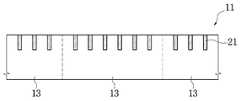
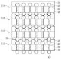
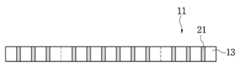
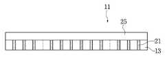
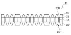
도 1은 본 발명의 제 1 실시 예에 적합한 웨이퍼를 보여주는 평면도이고, 도 2 내지 도 13은 본 발명의 제 1 실시 예에 따른 패키지-온-패키지 형성방법을 설명하기 위한 단면도들이다. 여기서, 도 2 내지 도 6 및 도 8은 도 1의 절단선 I-I'을 따라 취해진 단면도들이고, 도 7은 도 6의 K 부분을 상세히 보여주는 확대도이다.FIG. 1 is a plan view showing a wafer according to a first embodiment of the present invention, and FIGS. 2 to 13 are cross-sectional views illustrating a method of forming a package-on-package according to a first embodiment of the present invention. 2 to 6 and 8 are cross-sectional views taken along the line I-I 'of FIG. 1, and FIG. 7 is an enlarged view showing a detail K of FIG.
도 1 및 도 2를 참조하면, 본 발명의 제 1 실시 예에 따른 패키지-온-패키지 형성방법은 웨이퍼(11)에 다수의 관통 전극들(through silicon via; TSV; 21)을 형성하는 것을 포함할 수 있다. 상기 웨이퍼(11)는 다수의 반도체 칩들(13)을 구비할 수 있다. 상기 반도체 칩들(13)은 행 및 열 방향으로 2차원 배열된 구성을 보일 수 있다.Referring to FIGS. 1 and 2, a method of forming a package-on-package according to a first embodiment of the present invention includes forming a plurality of through-silicon vias (TSV) 21 on a
상기 관통 전극들(TSV; 21)은 텅스텐(W), 질화텅스텐(WN), 티타늄(Ti), 질화티타늄(TiN), 탄탈룸(Ta), 질화탄탈룸(TaN), 알루미늄(Al), 구리(Cu), 및 이들의 조합으로 이루어진 일군에서 선택된 적어도 하나와 같은 도전막으로 형성할 수 있다. 상기 관통 전극들(TSV; 21)은 상기 웨이퍼(11)의 일 표면으로부터 소정 깊이까지 침투하도록 형성할 수 있다. 즉, 상기 관통 전극들(TSV; 21)의 상단들은 상기 웨이퍼(11)의 일면에 노출될 수 있다. 상기 관통 전극들(TSV; 21)의 측벽들 및 하단들은 상기 웨이퍼(11)의 내부에 매립될 수 있다.The penetrating electrodes (TSV) 21 may be formed of at least one of tungsten (W), tungsten nitride (WN), titanium (Ti), titanium nitride (TiN), tantalum (Ta), tantalum (TaN) Cu), and a combination of these. The penetrating electrodes (TSV) 21 may be formed to penetrate from a surface of the
상기 웨이퍼(11)는 실리콘웨이퍼 또는 에스오아이(silicon on insulator; SOI)웨이퍼와 같은 반도체기판으로 형성할 수 있다. 상기 웨이퍼(11)에는 트랜지스터들, 정보저장요소들(data sotrage elements), 및/또는 상호배선들(interconnections)과 같이 상기 반도체 칩들(13)을 구성하기 위한 다양한 종류의 능동/수동소자들(도시하지 않음)이 형성될 수 있으나 간략한 설명을 위하여 생략하기로 한다. 본 발명의 제 1 실시 예에서, 상기 관통 전극들(TSV; 21)은 상기 능동/수동소자들(도시하지 않음)과 같은 면에 형성하는 경우를 상정하여 설명하기로 한다. 그러나 몇몇 다른 실시 예에서 상기 관통 전극들(TSV; 21)은 상기 능동/수동소자들(도시하지 않음)과 다른 면에 형성할 수도 있다.The
상기 반도체 칩들(13)은 디램(dynamic random access memory; DRAM) 및 에스램(static random access memory; SRAM)과 같은 휘발성 메모리 칩, 플래시메모리(flash memory), 상변화메모리(phase change memory), 엠램(magnetic random access memory; MRAM), 및 알램(resistive random access memory; RRAM)과 같은 비휘발성 메모리 칩, 로직소자(logic device) 및 마이크로프로세서(microprocessor)와 같은 비메모리 칩, 또는 이들의 조합을 구비할 수 있다.The semiconductor chips 13 may be a volatile memory chip such as a dynamic random access memory (DRAM) and a static random access memory (SRAM), a flash memory, a phase change memory, non-memory chips, such as non-volatile memory chips, logic devices and microprocessors, such as magnetic random access memory (MRAM) and resistive random access memory (RRAM) can do.
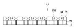
도 3을 참조하면, 상기 관통 전극들(TSV; 21) 상에 내부 접속단자들(23)을 형성할 수 있다. 상기 내부 접속단자들(23)은 도전성 범프(conductive bump), 솔더 볼(solder ball), 도전성 스페이서(conductive spacer), 핀 그리드 어레이(pin grid array; PGA), 리드 그리드 어레이(lead grid array; LGA), 및 이들의 조합으로 이루어진 일군에서 선택된 하나로 형성할 수 있다. 예를 들면, 상기 내부 접속단자들(23)은 솔더 볼(solder ball)을 부착하여 형성할 수 있다. 상기 내부 접속단자들(23)은 상기 관통 전극들(TSV; 21)의 상단들에 접촉될 수 있다. 몇몇 실시 예에서, 상기 내부 접속단자들(23)은 생략될 수 있다.Referring to FIG. 3,
도 4를 참조하면, 웨이퍼 레벨 몰딩(wafer level molding) 공정을 이용하여 상기 웨이퍼(11) 상에 봉지재(encapsulant; 25)를 형성할 수 있다. 상기 봉지재(25)는 상기 내부 접속단자들(23) 및 상기 관통 전극들(TSV; 21)을 덮을 수 있다. 상기 봉지재(25)는 수지 및 필러(filler)를 함유하는 에폭시 몰딩 컴파운드(epoxy molding compound; EMC)로 형성할 수 있다. 몇몇 실시 예에서, 상기 봉지재(25)는 언더필(under fill)과 같은 액상 수지를 이용하여 형성할 수도 있다.Referring to FIG. 4, an
도 5를 참조하면, 상기 웨이퍼(11)를 부분적으로 제거하여 상기 관통 전극들(TSV; 21)의 하단들을 노출할 수 있다. 예를 들면, 화학기계적연마(chemical mechanical polishing; CMP)공정, 에치백(etch-back)공정, 백그라인딩(backgrinding)공정, 및/또는 이들의 조합을 이용하여 상기 관통 전극들(TSV; 21)의 하단들이 노출될 때까지 상기 웨이퍼(11)의 후면을 부분적으로 제거할 수 있다. 그 결과, 상기 웨이퍼(11)의 두께는 현저히 감소할 수 있다. 상기 봉지재(25)는 상기 반도체 칩들(13) 및 상기 내부 접속단자들(23)을 물리적/화학적 손상으로부터 보호하는 역할을 할 수 있다.Referring to FIG. 5, the
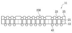
도 6을 참조하면, 상기 봉지재(25)를 관통하여 상기 내부 접속단자들(23)을 노출하는 개구부들(25H)을 형성할 수 있다. 상기 개구부들(25H)은 레이저 드릴링(laser drilling) 기술 또는 드라이 에치(dry etch) 기술을 사용하여 형성할 수 있다. 상기 개구부들(25H)은 몰드비아(mold via)로 명명할 수 있다. 상기 개구부들(25H)은 상기 관통 전극들(TSV; 21) 상에 정렬할 수 있다. 상기 개구부들(25H)은 상기 내부 접속단자들(23) 각각에 대응하는 크기를 구비할 수 있다. 상기 개구부들(25H)의 바닥에 상기 내부 접속단자들(23)의 상부표면들이 노출될 수 있다. 몇몇 실시 예에서, 상기 내부 접속단자들(23)이 생략된 경우 상기 개구부들(25H)의 바닥에 상기 관통 전극들(TSV; 21)의 상단들이 노출될 수 있다. 다른 실시 예에서, 상기 개구부들(25H)을 형성하는 공정은 상기 웨이퍼(11)를 부분적으로 제거하여 상기 관통 전극들(TSV; 21)을 노출하는 공정보다 선행하여 수행할 수도 있다. 또 다른 실시 예에서, 상기 개구부들(25H) 중 몇몇은 상기 관통 전극들(TSV;21)과 전기적으로 연결된 재배선 층(도시하지 않음)상에 정렬할 수 있다.Referring to FIG. 6,
도 7을 참조하여 도 6의 일부 영역(K)을 더욱 상세히 설명하기로 한다. 상기 반도체 칩(13)의 일면을 덮는 제 1 절연막(31)이 제공될 수 있다. 상기 관통 전극(TSV; 21)은 상기 제 1 절연막(31) 및 상기 반도체 칩(13)을 관통할 수 있다. 상기 관통 전극(TSV; 21) 및 상기 반도체 칩(13) 사이에 제 2 절연막(32)이 제공될 수 있다. 상기 제 2 절연막(32)은 상기 제 1 절연막(31)을 덮을 수 있다. 상기 관통 전극(TSV; 21)은 상기 제 2 절연막(32)에 의하여 상기 반도체 칩(13)에 대하여 전기적으로 절연될 수 있다. 상기 반도체 칩(13)의 다른 일면을 덮는 제 3 절연막(33)이 제공될 수 있다. 상기 제 1 절연막(31) 및 상기 제 3 절연막(33)은 서로 마주볼 수 있다. 상기 관통 전극(TSV; 21)은 상기 제 1 절연막(31) 및 상기 제 3 절연막(33)을 관통할 수 있다.The partial area K of Fig. 6 will be described in more detail with reference to Fig. A first insulating
상기 제 3 절연막(33)은, 상기 웨이퍼(11)를 부분적으로 제거하여 상기 관통 전극들(TSV; 21)을 노출하는 공정(도 5 참조)을 수행한 후, 형성된 것일 수 있다. 이와는 달리, 상기 제 3 절연막(33)은 상기 관통 전극들(TSV; 21)을 노출하기 전에 형성할 수도 있다.The third
상기 관통 전극(TSV; 21)의 양단들은 상기 반도체 칩(13)의 표면들과 실질적으로 동일평면 구성을 보이거나 상기 반도체 칩(13)의 표면들에 대하여 돌출되거나 함몰된 구성을 보일 수 있다. 예를 들면, 상기 관통 전극(TSV; 21)의 상단은 상기 반도체 칩(13)의 전면에 대하여 상대적으로 돌출될 수 있으며, 상기 관통 전극(TSV; 21)의 하단은 상기 반도체 칩(13)의 후면과 실질적으로 동일평면 구성을 보일 수 있다. 상기 관통 전극(TSV; 21)의 상단에 상기 내부 접속단자(23)가 부착될 수 있다.Both ends of the penetrating electrode (TSV) 21 may have substantially the same planar configuration as the surfaces of the
상기 반도체 칩(13)은 칩 패드(35)를 구비할 수 있다. 상기 제 1 절연막(31) 및 상기 제 2 절연막(32)은 상기 칩 패드(35) 및 상기 반도체 칩(13)을 덮을 수 있다. 상기 반도체 칩(13) 상에 상기 제 1 절연막(31) 및 상기 제 2 절연막(32)을 관통하여 상기 칩 패드(35)에 접촉된 재배선층(re-distribution layer; RDL; 37)을 형성할 수 있다. 상기 재배선층(RDL; 37)은 상기 칩 패드(35)를 경유하여 상기 반도체 칩(13) 내의 능동/수동소자들(도시하지 않음)에 전기적으로 접속될 수 있다.The
몇몇 실시 예에서, 상기 재배선층(RDL; 37)은 상기 관통 전극(TSV; 21)에 전기적으로 접속될 수 있다. 이 경우에, 상기 관통 전극(TSV; 21)은 상기 재배선층(RDL; 37) 및 상기 칩 패드(35)를 경유하여 상기 반도체 칩(13) 내의 능동/수동소자들(도시하지 않음)에 전기적으로 접속될 수 있다.In some embodiments, the redistribution layer (RDL) 37 may be electrically connected to the penetrating electrode (TSV) 21. In this case, the penetrating electrode (TSV) 21 is electrically connected to the active / passive elements (not shown) in the
상기 반도체 칩(13)의 일면은 상기 봉지재(25)로 덮일 수 있다. 즉, 상기 봉지재(25)는 상기 재배선층(RDL; 37), 상기 칩 패드(35), 상기 제 1 절연막(31), 상기 제 2 절연막(32), 및 상기 관통 전극(TSV; 21)을 덮을 수 있다. 상기 개구부(25H)에 의하여 상기 내부 접속단자(23)가 노출될 수 있다. 즉, 상기 개구부(25H)는 상기 관통 전극(TSV; 21)에 정렬할 수 있다.One side of the
몇몇 실시 예에서, 상기 재배선층(RDL; 37) 상에도 상기 개구부(25H)와 유사한 다른 개구부(도시하지 않음)를 형성할 수 있다. 즉, 상기 개구부들(도 6의 25H) 중 적어도 하나는 상기 재배선층(RDL; 37)에 정렬할 수 있다.In some embodiments, another opening (not shown) similar to the
상기 제 1 절연막(31), 상기 제 2 절연막(32), 및 상기 제 3 절연막(33)은 실리콘산화막, 실리콘질화막, 실리콘산질화막, 및 이들의 조합막으로 이루어진 일군에서 선택된 하나와 같은 절연막으로 형성할 수 있다. 상기 칩 패드(35)는 텅스텐(W), 질화텅스텐(WN), 티타늄(Ti), 질화티타늄(TiN), 탄탈룸(Ta), 질화탄탈룸(TaN), 알루미늄(Al), 구리(Cu), 및 이들의 조합으로 이루어진 일군에서 선택된 적어도 하나와 같은 도전막으로 형성할 수 있다. 상기 재배선층(RDL; 37)은 텅스텐(W), 질화텅스텐(WN), 티타늄(Ti), 질화티타늄(TiN), 탄탈룸(Ta), 질화탄탈룸(TaN), 알루미늄(Al), 구리(Cu), 및 이들의 조합으로 이루어진 일군에서 선택된 적어도 하나와 같은 도전막으로 형성할 수 있다.The first insulating
도 8을 참조하면, 상기 웨이퍼(11)의 일면에 외부 접속단자들(43)을 부착할 수 있다. 상기 외부 접속단자들(43)은 상기 관통 전극들(TSV; 21)의 하단들에 접촉할 수 있다. 상기 외부 접속단자들(43) 및 상기 내부 접속단자들(23)은 서로 마주볼 수 있다. 상기 외부 접속단자들(43)은 도전성 범프(conductive bump), 솔더 볼(solder ball), 도전성 스페이서(conductive spacer), 핀 그리드 어레이(pin grid array; PGA), 리드 그리드 어레이(lead grid array; LGA), 및 이들의 조합으로 이루어진 일군에서 선택된 하나로 형성할 수 있다. 예를 들면, 상기 외부 접속단자들(43)은 솔더 볼(solder ball) 부착 기술, 플레이팅(plating) 기술, 및/또는 스크린 프린팅(screen printing) 기술을 이용하여 형성할 수 있다.Referring to FIG. 8,
몇몇 실시 예에서, 상기 외부 접속단자들(43)은 생략될 수 있다.In some embodiments, the
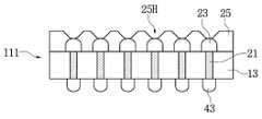
도 9를 참조하면, 상기 봉지재(25) 및 상기 웨이퍼(11)를 적당한 크기로 분할하여 다수의 반도체 패키지들을 형성할 수 있다. 상기 다수의 반도체 패키지들은 도 9에 도시된 제 1 반도체 패키지(111)와 유사한 구성을 보일 수 있다. 상기 제 1 반도체 패키지(111)는 상기 반도체 칩(13), 상기 봉지재(25), 상기 관통 전극들(TSV; 21), 상기 외부 접속단자들(43) 및 상기 내부 접속단자들(23)을 구비할 수 있다. 상기 봉지재(25) 및 상기 웨이퍼(11)를 적당한 크기로 분할하는 것은 싱귤레이션(singulation) 공정을 이용하여 수행할 수 있다.Referring to FIG. 9, the
상기 제 1 반도체 패키지(111)의 폭은 상기 반도체 칩(13)과 실질적으로 동일하게 형성할 수 있다. 상기 제 1 반도체 패키지(111)의 두께는 상기 봉지재(25) 및 상기 반도체 칩(13)에 의하여 결정될 수 있다. 결과적으로, 상기 제 1 반도체 패키지(111)의 크기는 종래에 비하여 현저히 감소할 수 있다.The width of the
몇몇 실시 예에서, 상기 봉지재(25) 및 상기 웨이퍼(11)를 적당한 크기로 분할한 후에, 상기 외부 접속단자들(43)을 형성할 수도 있다.In some embodiments, after the
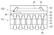
도 10을 참조하면, 본 발명의 제 1 실시 예에 따른 패키지-온-패키지(package on package; PoP) 형성방법은 상기 제 1 반도체 패키지(111) 상에 제 2 반도체 패키지(152)를 적층 하는 것을 포함할 수 있다. 상기 제 1 반도체 패키지(111)는 도 1 내지 도 9를 참조하여 설명한 것과 유사한 방법으로 형성할 수 있다.10, a method of forming a package on package (PoP) according to a first embodiment of the present invention includes stacking a
상기 제 2 반도체 패키지(152)는 인쇄회로기판(52) 상에 제 2 반도체 칩(53)을 부착하여 형성할 수 있다. 상기 제 2 반도체 칩(53)은 본딩 와이어(51)를 이용하여 상기 인쇄회로기판(52)에 전기적으로 접속할 수 있다. 상기 인쇄회로기판(52) 및 상기 제 2 반도체 칩(53)은 제 2 봉지재(55)로 덮을 수 있다. 상기 인쇄회로기판(52)의 일면에 제 2 외부 접속단자들(45)을 형성할 수 있다. 상기 제 2 반도체 칩(53)은 상기 본딩 와이어(51) 및 상기 인쇄회로기판(52)을 경유하여 상기 제 2 외부 접속단자들(45)에 전기적으로 접속될 수 있다.The
상기 인쇄회로기판(52)은 연성인쇄회로기판(flexible printed circuit board), 경성인쇄회로기판(rigid printed circuit board), 또는 이들의 조합으로 형성할 수 있다. 상기 본딩 와이어(51)는 와이어 본딩(wire bonding)기술, 빔 리드 본딩(beam lead bonding)기술, 테이프 본딩(tape bonding)기술, 및 이들의 조합으로 이루어진 일군에서 선택된 하나를 이용하여 형성할 수 있다. 상기 본딩 와이어(51)는 골드 와이어(gold wire), 알루미늄 와이어(aluminum wire), 빔 리드(beam lead), 도전성 테이프(conductive tape), 및 이들의 조합으로 이루어진 일군에서 선택된 하나일 수 있다.The printed
상기 제 2 반도체 칩(53)은 디램(dynamic random access memory; DRAM) 및 에스램(static random access memory; SRAM)과 같은 휘발성 메모리 칩, 플래시메모리(flash memory), 상변화메모리(phase change memory), 엠램(magnetic random access memory; MRAM), 및 알램(resistive random access memory; RRAM)과 같은 비휘발성 메모리 칩, 로직소자(logic device) 및 마이크로프로세서(microprocessor)와 같은 비메모리 칩, 또는 이들의 조합을 구비할 수 있다. 상기 제 2 외부 접속단자들(45)은 도전성 범프(conductive bump), 솔더 볼(solder ball), 도전성 스페이서(conductive spacer), 핀 그리드 어레이(pin grid array; PGA), 리드 그리드 어레이(lead grid array; LGA), 및 이들의 조합으로 이루어진 일군에서 선택된 하나로 형성할 수 있다.The
상기 제 1 반도체 패키지(111) 및 상기 제 2 반도체 패키지(152) 사이에 언더필(under fill; 39)을 형성할 수 있다. 상기 제 2 외부 접속단자들(45)은 상기 언더필(39)을 관통하여 상기 내부 접속단자들(23)에 접촉할 수 있다. 결과적으로, 상기 외부 접속단자들(43)은 상기 관통 전극들(TSV; 21), 상기 내부 접속단자들(23), 상기 제 2 외부 접속단자들(45), 상기 인쇄회로기판(52), 및 상기 본딩 와이어(51)를 경유하여 상기 제 2 반도체 칩(53)에 전기적으로 접속될 수 있다.An under
상기 제 1 반도체 패키지(111)의 폭은 상기 반도체 칩(13)과 실질적으로 동일하게 형성할 수 있다. 상기 제 1 반도체 패키지(111)의 두께는 상기 봉지재(25) 및 상기 반도체 칩(13)에 의하여 결정될 수 있다. 상기 인쇄회로기판(52)의 폭은 상기 제 1 반도체 패키지(111)와 실질적으로 동일하거나 상기 제 1 반도체 패키지(111)보다 작은 크기로 형성할 수 있다. 즉, 상기 제 2 반도체 패키지(152)의 폭은 상기 제 1 반도체 패키지(111)와 실질적으로 동일하거나 상기 제 1 반도체 패키지(111)보다 작은 크기로 형성할 수 있다. 결과적으로, 본 발명의 제 1 실시 예에 따르면 상기 반도체 칩(13) 외곽에 상기 제 1 반도체 패키지(111)와 상기 제 2 반도체 패키지(152)를 전기적으로 연결하기 위한 추가적인 전기적 수단을 생략할 수 있어 패키지-온-패키지(package on package; PoP)의 크기를 종래에 비하여 현저히 축소할 수 있다.The width of the
다른 실시 예에서, 상기 인쇄회로기판(52)의 폭은 상기 제 1 반도체 패키지(111)보다 클 수 있다. 즉, 상기 제 2 반도체 패키지(152)의 폭은 상기 제 1 반도체 패키지(111)보다 클 수 있다.In another embodiment, the width of the printed
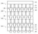
도 11을 참조하면, 본 발명의 몇몇 실시 예에 따른 패키지-온-패키지(package on package; PoP) 형성방법은 상기 제 1 반도체 패키지(111) 상에 상기 제 2 반도체 패키지(152) 및 제 3 반도체 패키지(112)를 적층 하는 것을 포함할 수 있다. 상기 제 1 반도체 패키지(111) 및 상기 제 3 반도체 패키지(112)는 도 1 내지 도 9를 참조하여 설명한 것과 유사한 방법으로 형성할 수 있다. 상기 제 2 반도체 패키지(152)는 도 10을 참조하여 설명한 것과 유사한 것일 수 있다. 상기 제 3 반도체 패키지(112)는 상기 제 1 반도체 패키지(111) 및 상기 제 2 반도체 패키지(152) 사이에 적층 할 수 있다.11, a method for forming a package on package (PoP) according to some embodiments of the present invention includes forming a
도 12를 참조하면, 본 발명의 몇몇 실시 예에 따른 패키지-온-패키지(package on package; PoP) 형성방법은 제 2 인쇄회로기판(63) 상에 상기 제 1 반도체 패키지(111) 및 상기 제 2 반도체 패키지(152)를 차례로 적층 하는 것을 포함할 수 있다. 상기 제 1 반도체 패키지(111)는 도 1 내지 도 9를 참조하여 설명한 것과 유사한 방법으로 형성할 수 있다. 상기 제 2 반도체 패키지(152)는 도 10을 참조하여 설명한 것과 유사한 것일 수 있다.12, a method of forming a package on package (PoP) according to some embodiments of the present invention includes forming a
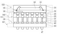
상기 제 2 인쇄회로기판(63)은 연성인쇄회로기판(flexible printed circuit board), 경성인쇄회로기판(rigid printed circuit board), 또는 이들의 조합으로 형성할 수 있다. 상기 제 2 인쇄회로기판(63) 및 상기 제 1 반도체 패키지(111) 사이에 언더필(39)을 형성할 수 있다. 상기 외부 접속단자들(43)은 상기 언더필(39)을 관통하여 상기 제 2 인쇄회로기판(63)에 접촉할 수 있다.The second printed
상기 제 2 인쇄회로기판(63)의 일면에 기판 접속단자들(47)을 형성할 수 있다. 상기 기판 접속단자들(47)은 도전성 범프(conductive bump), 솔더 볼(solder ball), 도전성 스페이서(conductive spacer), 핀 그리드 어레이(pin grid array; PGA), 리드 그리드 어레이(lead grid array; LGA), 및 이들의 조합으로 이루어진 일군에서 선택된 하나로 형성할 수 있다.And
상기 반도체 칩(13) 및 상기 제 2 반도체 칩(53)은 상기 관통 전극들(TSV; 21) 및 상기 제 2 인쇄회로기판(63)을 경유하여 상기 기판 접속단자들(47)에 전기적으로 접속될 수 있다. 이에 따라, 상기 제 2 인쇄회로기판(63)은 우회 접속단자들(143)을 배치하기 위한 여분의 공간(63')을 필요로 하지않는다.The
상기 제 1 반도체 패키지(111)의 폭은 상기 반도체 칩(13)에 의하여 결정될 수 있다. 예를 들면, 상기 제 1 반도체 패키지(111)의 폭은 상기 반도체 칩(13)과 실질적으로 동일할 수 있다. 상기 제 2 인쇄회로기판(63)의 폭은 상기 제 1 반도체 패키지(111)에 의하여 결정될 수 있다. 예를 들면, 상기 제 2 인쇄회로기판(63)의 폭은 상기 제 1 반도체 패키지(111)와 실질적으로 동일하거나 상기 제 1 반도체 패키지(111)보다 작을 수 있다. 이에 더하여, 상기 제 2 반도체 패키지(152)의 폭 또한 상기 제 1 반도체 패키지(111)와 실질적으로 동일하거나 상기 제 1 반도체 패키지(111)보다 작을 수 있다. 결론적으로, 본 발명의 몇몇 실시 예에 따르면 상기 패키지-온-패키지(PoP)의 크기를 종래에 비하여 현저히 축소할 수 있다.The width of the
다른 실시 예에서, 상기 제 2 반도체 패키지(152)의 폭은 상기 제 1 반도체 패키지(111)보다 클 수 있다.In another embodiment, the width of the
도 13을 참조하면, 본 발명의 몇몇 실시 예에 따른 패키지-온-패키지(package on package; PoP) 형성방법은 상기 제 1 반도체 패키지(111) 상에 상기 제 3 반도체 패키지(112), 제 4 반도체 패키지(113), 및 제 5 반도체 패키지(114)를 차례로 적층 하는 것을 포함할 수 있다. 상기 제 1 반도체 패키지(111), 상기 제 3 반도체 패키지(112), 상기 제 4 반도체 패키지(113), 및 상기 제 5 반도체 패키지(114)는 도 1 내지 도 9를 참조하여 설명한 것과 유사한 방법으로 형성할 수 있다. 상기 제 5 반도체 패키지(114)는 상기 개구부들(도 6의 25H)을 형성하는 공정을 생략하여 형성할 수 있다.13, a method of forming a package on package (PoP) according to some embodiments of the present invention includes forming a
다른 실시 예에서, 상기 제 5 반도체 패키지(114)는 상기 내부 접속단자들(도 3의 23)을 형성하는 공정을 생략하여 형성할 수도 있다. 또 다른 실시 예에서, 상기 제 5 반도체 패키지(114)는 상기 관통 전극들(TSV; 21)을 포함하지 않을 수 있다.In another embodiment, the
[실시예 2][Example 2]
도 14 내지 도 20은 본 발명의 제 2 실시 예에 따른 패키지-온-패키지 형성방법을 설명하기 위한 단면도들이다.14 to 20 are sectional views for explaining a method of forming a package-on-package according to a second embodiment of the present invention.
도 14를 참조하면, 본 발명의 제 2 실시 예에 따른 패키지-온-패키지(package on package; PoP) 형성방법은 웨이퍼(11)에 다수의 관통 전극들(through silicon via; TSV; 21)을 형성하는 것을 포함할 수 있다. 상기 웨이퍼(11)는 다수의 반도체 칩들(13)을 구비할 수 있다. 상기 관통 전극들(TSV; 21)은 상기 웨이퍼(11)의 일 표면으로부터 소정깊이까지 침투하도록 형성할 수 있다.14, a method for forming a package on package (PoP) according to a second embodiment of the present invention includes forming a plurality of through silicon via (TSV) . ≪ / RTI > The
웨이퍼 레벨 몰딩(wafer level molding) 공정을 이용하여 상기 웨이퍼(11) 상에 봉지재(encapsulant; 25)를 형성할 수 있다. 상기 봉지재(25)는 상기 관통 전극들(TSV; 21)을 덮을 수 있다. 상기 봉지재(25)는 수지 및 필러(filler)를 함유하는 에폭시 몰딩 컴파운드(epoxy molding compound; EMC)로 형성할 수 있다. 몇몇 실시 예에서, 상기 봉지재(25)는 언더필(under fill)과 같은 액상 수지를 이용하여 형성할 수도 있다.An
도 15를 참조하면, 상기 웨이퍼(11)를 부분적으로 제거하여 상기 관통 전극들(TSV; 21)을 노출할 수 있다. 예를 들면, 화학기계적연마(chemical mechanical polishing; CMP)공정, 에치백(etch-back)공정, 백그라인딩(backgrinding)공정, 및/또는 이들의 조합을 이용하여 상기 관통 전극들(TSV; 21)의 일단들이 노출될 때까지 상기 웨이퍼(11)의 후면을 부분적으로 제거할 수 있다. 그 결과, 상기 웨이퍼(11)의 두께는 현저히 감소할 수 있다.Referring to FIG. 15, the
상기 봉지재(25)를 관통하여 상기 관통 전극들(TSV; 21)을 노출하는 개구부들(25H)을 형성할 수 있다. 상기 개구부들(25H)은 레이저 드릴링(laser drilling) 기술 또는 드라이 에치(dry etch) 기술을 사용하여 형성할 수 있다. 상기 개구부들(25H)은 몰드비아(mold via)로 명명할 수 있다. 상기 개구부들(25H)의 바닥에 상기 관통 전극들(TSV; 21)의 상부표면들이 노출될 수 있다. 몇몇 실시 예에서, 상기 개구부들(25H)을 형성하는 공정은 상기 웨이퍼(11)를 부분적으로 제거하여 상기 관통 전극들(TSV; 21)을 노출하는 공정보다 선행하여 수행할 수도 있다.
상기 웨이퍼(11)의 일면에 외부 접속단자들(43)을 부착할 수 있다. 상기 관통 전극들(TSV; 21)의 일단들은 상기 외부 접속단자들(43)에 접촉할 수 있으며, 상기 관통 전극들(TSV; 21)의 다른 일단들은 상기 개구부들(25H)에 노출될 수 있다. 몇몇 실시 예에서, 상기 외부 접속단자들(43)은 생략될 수 있다. 다른 실시 예에서, 상기 외부 접속단자들(43)은 상기 개구부들(25H)을 형성하는 공정보다 선행하여 형성할 수도 있다.
도 16을 참조하면, 상기 봉지재(25) 및 상기 웨이퍼(11)를 적당한 크기로 분할하여 다수의 반도체 패키지들을 형성할 수 있다. 상기 다수의 반도체 패키지들은 도 16에 도시된 제 1 반도체 패키지(111)와 유사한 구성을 보일 수 있다. 상기 제 1 반도체 패키지(111)는 상기 반도체 칩(13), 상기 봉지재(25), 상기 관통 전극들(TSV; 21), 및 상기 외부 접속단자들(43)을 구비할 수 있다. 상기 봉지재(25) 및 상기 웨이퍼(11)를 적당한 크기로 분할하는 것은 싱귤레이션(singulation) 공정을 이용하여 수행할 수 있다.Referring to FIG. 16, the
몇몇 실시 예에서, 상기 봉지재(25) 및 상기 웨이퍼(11)를 적당한 크기로 분할한 후에, 상기 외부 접속단자들(43)을 형성할 수도 있다.In some embodiments, after the
도 17을 참조하면, 본 발명의 제 2 실시 예에 따른 패키지-온-패키지(package on package; PoP) 형성방법은 상기 제 1 반도체 패키지(111) 상에 제 2 반도체 패키지(152)를 적층 하는 것을 포함할 수 있다. 상기 제 1 반도체 패키지(111)는 도 14 내지 도 16을 참조하여 설명한 것과 유사한 방법으로 형성할 수 있다.17, a method of forming a package on package (PoP) according to a second embodiment of the present invention includes stacking a
상기 제 2 반도체 패키지(152)는 인쇄회로기판(52) 상에 제 2 반도체 칩(53)을 부착하여 형성할 수 있다. 상기 제 2 반도체 칩(53)은 본딩 와이어(51)를 이용하여 상기 인쇄회로기판(52)에 전기적으로 접속할 수 있으며, 플립칩 본딩 방식으로 접속할 수도 있다. 상기 인쇄회로기판(52) 및 상기 제 2 반도체 칩(53)은 제 2 봉지재(55)로 덮을 수 있다. 상기 인쇄회로기판(52)의 일면에 제 2 외부 접속단자들(45)을 형성할 수 있다. 상기 제 2 반도체 칩(53)은 상기 본딩 와이어(51) 및 상기 인쇄회로기판(52)을 경유하여 상기 제 2 외부 접속단자들(45)에 전기적으로 접속될 수 있다.The
상기 제 1 반도체 패키지(111) 및 상기 제 2 반도체 패키지(152) 사이에 언더필(under fill; 39)을 형성할 수 있다. 상기 제 2 외부 접속단자들(45)은 상기 언더필(39)을 관통하여 상기 관통 전극들(TSV; 21)에 접촉할 수 있다. 결과적으로, 상기 외부 접속단자들(43)은 상기 관통 전극들(TSV; 21), 상기 제 2 외부 접속단자들(45), 상기 인쇄회로기판(52), 및 상기 본딩 와이어(51)를 경유하여 상기 제 2 반도체 칩(53)에 전기적으로 접속될 수 있다.An under
도 18을 참조하면, 본 발명의 몇몇 실시 예에 따른 패키지-온-패키지(package on package; PoP) 형성방법은 상기 제 1 반도체 패키지(111) 상에 상기 제 2 반도체 패키지(152) 및 제 3 반도체 패키지(112)를 적층 하는 것을 포함할 수 있다. 상기 제 1 반도체 패키지(111) 및 상기 제 3 반도체 패키지(112)는 도 14 내지 도 16을 참조하여 설명한 것과 유사한 방법으로 형성할 수 있다. 상기 제 2 반도체 패키지(152)는 도 17을 참조하여 설명한 것과 유사한 것일 수 있다. 상기 제 3 반도체 패키지(112)는 상기 제 1 반도체 패키지(111) 및 상기 제 2 반도체 패키지(152) 사이에 적층 할 수 있다.18, a method of forming a package on package (PoP) according to some embodiments of the present invention includes forming a
도 19를 참조하면, 본 발명의 몇몇 실시 예에 따른 패키지-온-패키지(package on package; PoP) 형성방법은 제 2 인쇄회로기판(63) 상에 상기 제 1 반도체 패키지(111) 및 상기 제 2 반도체 패키지(152)를 차례로 적층 하는 것을 포함할 수 있다. 상기 제 1 반도체 패키지(111)는 도 14 내지 도 16을 참조하여 설명한 것과 유사한 방법으로 형성할 수 있다. 상기 제 2 반도체 패키지(152)는 도 17을 참조하여 설명한 것과 유사한 것일 수 있다. 상기 제 2 인쇄회로기판(63) 및 상기 제 1 반도체 패키지(111) 사이에 언더필(39)을 형성할 수 있다. 상기 외부 접속단자들(43)은 상기 언더필(39)을 관통하여 상기 제 2 인쇄회로기판(63)에 접촉할 수 있다. 상기 제 2 인쇄회로기판(63)의 일면에 기판 접속단자들(47)을 형성할 수 있다. 상기 반도체 칩(13) 및 상기 제 2 반도체 칩(53)은 상기 관통 전극들(TSV; 21) 및 상기 제 2 인쇄회로기판(63)을 경유하여 상기 기판 접속단자들(47)에 전기적으로 접속될 수 있다.19, a method of forming a package on package (PoP) according to some embodiments of the present invention includes forming a
상기 제 1 반도체 패키지(111)의 폭은 상기 반도체 칩(13)에 의하여 결정될 수 있다. 예를 들면, 상기 제 1 반도체 패키지(111)의 폭은 상기 반도체 칩(13)과 실질적으로 동일할 수 있다. 상기 제 2 인쇄회로기판(63)의 폭은 상기 제 1 반도체 패키지(111)에 의하여 결정될 수 있다. 예를 들면, 상기 제 2 인쇄회로기판(63)의 폭은 상기 제 1 반도체 패키지(111)와 실질적으로 동일하거나 상기 제 1 반도체 패키지(111)보다 작을 수 있다. 이에 더하여, 상기 제 2 반도체 패키지(152)의 폭 또한 상기 제 1 반도체 패키지(111)와 실질적으로 동일하거나 상기 제 1 반도체 패키지(111)보다 작을 수 있다. 결론적으로, 본 발명의 몇몇 실시 예에 따르면 상기 패키지-온-패키지(PoP)의 크기를 종래에 비하여 현저히 축소할 수 있다.The width of the
다른 실시 예에서, 상기 제 2 인쇄회로기판(63)의 폭은 상기 제 1 반도체 패키지(111)보다 클 수 있다.In another embodiment, the width of the second printed
도 20을 참조하면, 본 발명의 몇몇 실시 예에 따른 패키지-온-패키지(package on package; PoP) 형성방법은 상기 제 1 반도체 패키지(111) 상에 상기 제 3 반도체 패키지(112), 제 4 반도체 패키지(113), 및 제 5 반도체 패키지(114)를 차례로 적층 하는 것을 포함할 수 있다. 상기 제 1 반도체 패키지(111), 상기 제 3 반도체 패키지(112), 상기 제 4 반도체 패키지(113), 및 상기 제 5 반도체 패키지(114)는 도 14 내지 도 16을 참조하여 설명한 것과 유사한 방법으로 형성할 수 있다. 상기 제 5 반도체 패키지(114)는 상기 개구부들(도 15의 25H)을 형성하는 공정을 생략하여 형성할 수 있다.20, a method for forming a package on package (PoP) according to some embodiments of the present invention includes forming a
[실시예 3][Example 3]
도 21 및 도 22는 본 발명의 제 3 실시 예에 따른 패키지-온-패키지(package on package; PoP) 형성방법을 설명하기 위한 단면도들이다.21 and 22 are sectional views for explaining a package on package (PoP) forming method according to a third embodiment of the present invention.
도 21을 참조하면, 본 발명의 제 3 실시 예에 따른 패키지-온-패키지(package on package; PoP) 형성방법은 웨이퍼(11)에 다수의 관통 전극들(through silicon via; TSV; 21)을 형성하는 것을 포함할 수 있다. 상기 웨이퍼(11)는 다수의 반도체 칩들(13)을 구비할 수 있다. 상기 웨이퍼(11)를 부분적으로 제거하여 상기 관통 전극들(TSV; 21)을 노출할 수 있다. 예를 들면, 화학기계적연마(chemical mechanical polishing; CMP)공정, 에치백(etch-back)공정, 백그라인딩(backgrinding)공정, 및/또는 이들의 조합을 이용하여 상기 관통 전극들(TSV; 21)의 일단들이 노출될 때까지 상기 웨이퍼(11)의 후면을 부분적으로 제거할 수 있다. 그 결과, 상기 웨이퍼(11)의 두께는 현저히 감소할 수 있다. 상기 관통 전극들(TSV; 21)의 일단들은 상기 웨이퍼(11)의 일면에 노출될 수 있으며, 상기 관통 전극들(TSV; 21)의 다른 단들은 상기 웨이퍼(11)의 다른 일면에 노출될 수 있다.21, a method of forming a package on package (PoP) according to a third embodiment of the present invention includes forming a plurality of through silicon via (TSV) . ≪ / RTI > The
도 22를 참조하면, 상기 관통 전극들(TSV; 21) 상에 내부 접속단자들(23)을 형성할 수 있다. 상기 내부 접속단자들(23)은 도전성 범프(conductive bump), 솔더 볼(solder ball), 도전성 스페이서(conductive spacer), 핀 그리드 어레이(pin grid array; PGA), 리드 그리드 어레이(lead grid array; LGA), 및 이들의 조합으로 이루어진 일군에서 선택된 하나로 형성할 수 있다. 상기 내부 접속단자들(23)은 상기 관통 전극들(TSV; 21)에 접촉될 수 있다.Referring to FIG. 22,
상기 내부 접속단자들(23)은 상기 웨이퍼(11)의 상면(front side)에 형성할 수 있다. 즉, 상기 내부 접속단자들(23)은 상기 웨이퍼(11)에 형성된 능동/수동소자들(도시하지 않음)과 같은 면에 형성할 수 있다. 이와 다르게, 상기 내부 접속단자들(23)은 상기 웨이퍼(11)의 후면(back side)에 형성할 수도 있다. 몇몇 실시 예에서, 상기 내부 접속단자들(23)은 생략될 수 있다.The
웨이퍼 레벨 몰딩(wafer level molding) 공정을 이용하여 상기 웨이퍼(11) 상에 봉지재(encapsulant; 25)를 형성할 수 있다. 상기 봉지재(25)는 상기 내부 접속단자들(23) 및 상기 관통 전극들(TSV; 21)을 덮을 수 있다. 상기 봉지재(25)는 수지 및 필러(filler)를 함유하는 에폭시 몰딩 컴파운드(epoxy molding compound; EMC)로 형성할 수 있다. 몇몇 실시 예에서, 상기 봉지재(25)는 언더필(under fill)과 같은 액상 수지를 이용하여 형성할 수도 있다. 여기서, 상기 웨이퍼(11)의 일면은 노출될 수 있다.An
상기 봉지재(25)를 관통하여 상기 내부 접속단자들(23)을 노출하는 개구부들(25H)을 형성할 수 있다. 상기 개구부들(25H)은 레이저 드릴링(laser drilling) 기술 또는 드라이 에치(dry etch) 기술을 사용하여 형성할 수 있다. 상기 개구부들(25H)은 몰드비아(mold via)로 명명할 수 있다. 상기 개구부들(25H)의 바닥에 상기 내부 접속단자들(23)의 상부표면들이 노출될 수 있다. 몇몇 실시 예에서, 상기 내부 접속단자들(23)이 생략된 경우 상기 개구부들(25H)의 바닥에 상기 관통 전극들(TSV; 21)이 노출될 수 있다.It is possible to form
이후, 도 7 내지 도 13 을 참조하여 설명한 것과 유사한 방법으로 패키지-온-패키지(package on package; PoP)를 형성할 수 있다.Thereafter, a package on package (PoP) may be formed in a manner similar to that described with reference to FIGS.
[실시예 4][Example 4]
도 23은 본 발명의 제 4 실시 예에 따른 패키지-온-패키지(package on package; PoP) 형성방법을 설명하기 위한 단면도이다.23 is a sectional view for explaining a package on package (PoP) forming method according to a fourth embodiment of the present invention.
도 23을 참조하면, 본 발명의 제 4 실시 예에 따른 패키지-온-패키지(package on package; PoP) 형성방법은 웨이퍼(11)에 다수의 관통 전극들(through silicon via; TSV; 21)을 형성하는 것을 포함할 수 있다. 상기 웨이퍼(11)는 다수의 반도체 칩들(13)을 구비할 수 있다. 상기 웨이퍼(11)를 부분적으로 제거하여 상기 관통 전극들(TSV; 21)을 노출할 수 있다. 예를 들면, 화학기계적연마(chemical mechanical polishing; CMP)공정, 에치백(etch-back)공정, 백그라인딩(backgrinding)공정, 및/또는 이들의 조합을 이용하여 상기 관통 전극들(TSV; 21)의 일단들이 노출될 때까지 상기 웨이퍼(11)의 후면을 부분적으로 제거할 수 있다. 그 결과, 상기 웨이퍼(11)의 두께는 현저히 감소할 수 있다. 상기 관통 전극들(TSV; 21)의 일단들은 상기 웨이퍼(11)의 일면에 노출될 수 있으며, 상기 관통 전극들(TSV; 21)의 다른 단들은 상기 웨이퍼(11)의 다른 일면에 노출될 수 있다.23, a method of forming a package on package (PoP) according to a fourth embodiment of the present invention includes forming a plurality of through silicon vias (TSV) 21 on a
웨이퍼 레벨 몰딩(wafer level molding) 공정을 이용하여 상기 웨이퍼(11) 상에 봉지재(encapsulant; 25)를 형성할 수 있다. 상기 봉지재(25)는 상기 관통 전극들(TSV; 21)을 덮을 수 있다. 상기 봉지재(25)는 수지 및 필러(filler)를 함유하는 에폭시 몰딩 컴파운드(epoxy molding compound; EMC)로 형성할 수 있다. 몇몇 실시 예에서, 상기 봉지재(25)는 언더필(under fill)과 같은 액상 수지를 이용하여 형성할 수도 있다.An
상기 봉지재(25)는 상기 웨이퍼(11)의 상면(front side)에 형성할 수 있다. 즉, 상기 봉지재(25)는 상기 웨이퍼(11)에 형성된 능동/수동소자들(도시하지 않음)과 같은 면에 형성할 수 있다. 이와 다르게, 상기 봉지재(25)는 상기 웨이퍼(11)의 후면(back side)에 형성할 수도 있다. 여기서, 상기 웨이퍼(11)의 일면은 노출될 수 있다.The
이후, 도 15 내지 도 20 을 참조하여 설명한 것과 유사한 방법으로 패키지-온-패키지(package on package; PoP)를 형성할 수 있다.Thereafter, a package on package (PoP) can be formed in a manner similar to that described with reference to Figs. 15 to 20.
[실시예 5][Example 5]
도 24 내지 도 26은 본 발명의 제 5 실시 예에 따른 패키지-온-패키지 형성방법을 설명하기 위한 단면도들이다.24 to 26 are sectional views for explaining a method of forming a package-on-package according to a fifth embodiment of the present invention.
도 24를 참조하면, 본 발명의 제 5 실시 예에 따른 패키지-온-패키지(package on package; PoP) 형성방법은 웨이퍼(11)에 다수의 관통 전극들(through silicon via; TSV; 21)을 형성하는 것을 포함할 수 있다. 상기 웨이퍼(11)는 다수의 반도체 칩들(13)을 구비할 수 있다. 상기 웨이퍼(11)를 부분적으로 제거하여 상기 관통 전극들(TSV; 21)을 노출할 수 있다. 예를 들면, 화학기계적연마(chemical mechanical polishing; CMP)공정, 에치백(etch-back)공정, 백그라인딩(backgrinding)공정, 및/또는 이들의 조합을 이용하여 상기 관통 전극들(TSV; 21)의 일단들이 노출될 때까지 상기 웨이퍼(11)의 후면을 부분적으로 제거할 수 있다. 그 결과, 상기 웨이퍼(11)의 두께는 현저히 감소할 수 있다. 상기 관통 전극들(TSV; 21)의 일단들은 상기 웨이퍼(11)의 일면에 노출될 수 있으며, 상기 관통 전극들(TSV; 21)의 다른 단들은 상기 웨이퍼(11)의 다른 일면에 노출될 수 있다.24, a method of forming a package on package (PoP) according to a fifth embodiment of the present invention includes forming a plurality of through silicon via (TSV) . ≪ / RTI > The
웨이퍼 레벨 몰딩(wafer level molding) 공정을 이용하여 상기 웨이퍼(11)의 서로 마주보는 양면을 덮는 봉지재(encapsulant; 25, 25')를 형성할 수 있다. 상기 봉지재(25, 25')는 상기 관통 전극들(TSV; 21)을 덮을 수 있다. 상기 봉지재(25, 25')는 수지 및 필러(filler)를 함유하는 에폭시 몰딩 컴파운드(epoxy molding compound; EMC)로 형성할 수 있다. 몇몇 실시 예에서, 상기 봉지재(25, 25')는 언더필(under fill)과 같은 액상 수지를 이용하여 형성할 수도 있다. 상기 봉지재(25, 25')는 제 1 봉지재(25) 및 제 2 봉지재(25')로 구별할 수 있다.
상기 봉지재(25, 25')를 관통하여 상기 관통 전극들(TSV; 21)을 노출하는 개구부들(25H, 25H')을 형성할 수 있다. 상기 개구부들(25H, 25H')은 레이저 드릴링(laser drilling) 기술을 사용하여 형성할 수 있다. 상기 개구부들(25H, 25H')은 몰드비아(mold via)로 명명할 수 있다. 상기 개구부들(25H, 25H')의 바닥에 상기 관통 전극들(TSV; 21)의 표면들이 노출될 수 있다. 상기 개구부들(25H, 25H')은 제 1 개구부(25H) 및 제 2 개구부(25H')로 구별할 수 있다.The
도 25를 참조하면, 상기 웨이퍼(11)의 하부 및 상부에 하부 접속단자들(49) 및 상부 접속단자들(49')을 부착할 수 있다. 상기 관통 전극들(TSV; 21)의 일단들은 상기 하부 접속단자들(49)에 접촉할 수 있으며, 상기 관통 전극들(TSV; 21)의 다른 일단들은 상기 상부 접속단자들(49')에 접촉할 수 있다. 몇몇 실시 예에서, 상기 하부 접속단자들(49) 및 상기 상부 접속단자들(49')은 선택적으로 생략될 수 있다. 예를 들면, 상기 상부 접속단자들(49')은 모두 생략될 수 있다. 상기 하부 접속단자들(49) 및 상기 상부 접속단자들(49')은 상기 봉지재(25, 25')의 표면들보다 상대적으로 돌출될 수 있다.Referring to FIG. 25,
상기 하부 접속단자들(49)은 도전성 범프(conductive bump), 솔더 볼(solder ball), 도전성 스페이서(conductive spacer), 핀 그리드 어레이(pin grid array; PGA), 리드 그리드 어레이(lead grid array; LGA), 및 이들의 조합으로 이루어진 일군에서 선택된 하나로 형성할 수 있다. 상기 상부 접속단자들(49')은 도전성 범프(conductive bump), 솔더 볼(solder ball), 도전성 스페이서(conductive spacer), 핀 그리드 어레이(pin grid array; PGA), 리드 그리드 어레이(lead grid array; LGA), 및 이들의 조합으로 이루어진 일군에서 선택된 하나로 형성할 수 있다.The
상기 봉지재(25, 25') 및 상기 웨이퍼(11)를 적당한 크기로 분할하여 다수의 반도체 패키지들을 형성할 수 있다. 상기 다수의 반도체 패키지들은 도 26에 도시된 제 1 반도체 패키지(111)와 유사한 구성을 보일 수 있다. 상기 제 1 반도체 패키지(111)는 상기 반도체 칩(13), 상기 봉지재(25, 25'), 상기 관통 전극들(TSV; 21), 상기 하부 접속단자들(49) 및 상기 상부 접속단자들(49')을 구비할 수 있다. 상기 봉지재(25, 25') 및 상기 웨이퍼(11)를 적당한 크기로 분할하는 것은 싱귤레이션(singulation) 공정을 이용하여 수행할 수 있다.The
몇몇 실시 예에서, 상기 봉지재(25, 25') 및 상기 웨이퍼(11)를 적당한 크기로 분할한 후에, 상기 하부 접속단자들(49) 및 상기 상부 접속단자들(49')을 형성할 수도 있다.In some embodiments, it is possible to form the
도 26을 참조하면, 본 발명의 제 5 실시 예에 따른 패키지-온-패키지(package on package; PoP) 형성방법은 상기 제 1 반도체 패키지(111) 상에 제 2 반도체 패키지(152)를 적층 하는 것을 포함할 수 있다. 상기 제 1 반도체 패키지(111)는 도 24 및 도 25를 참조하여 설명한 것과 유사한 방법으로 형성할 수 있다.26, a method for forming a package on package (PoP) according to a fifth embodiment of the present invention includes stacking a
상기 제 2 반도체 패키지(152)는 인쇄회로기판(52) 상에 제 2 반도체 칩(53)을 부착하여 형성할 수 있다. 상기 제 2 반도체 칩(53)은 본딩 와이어(51)를 이용하거나 플립칩 본딩 방식으로 상기 인쇄회로기판(52)에 전기적으로 접속할 수 있다. 상기 인쇄회로기판(52) 및 상기 제 2 반도체 칩(53)은 제 2 봉지재(55)로 덮을 수 있다. 상기 인쇄회로기판(52)의 일면에 제 2 외부 접속단자들(45)을 형성할 수 있다. 상기 제 2 반도체 칩(53)은 상기 본딩 와이어(51) 및 상기 인쇄회로기판(52)을 경유하여 상기 제 2 외부 접속단자들(45)에 전기적으로 접속될 수 있다.The
상기 제 1 반도체 패키지(111) 및 상기 제 2 반도체 패키지(152) 사이에 언더필(under fill; 39)을 형성할 수 있다. 상기 제 2 외부 접속단자들(45)은 상기 언더필(39)을 관통하여 상기 관통 전극들(TSV; 21)에 접촉할 수 있다. 결과적으로, 상기 하부 접속단자들(49)은 상기 관통 전극들(TSV; 21), 상기 제 2 외부 접속단자들(45), 상기 인쇄회로기판(52), 및 상기 본딩 와이어(51)를 경유하여 상기 제 2 반도체 칩(53)에 전기적으로 접속될 수 있다.An under
[실시예 6][Example 6]
도 27은 본 발명의 제 6 실시 예에 따른 패키지-온-패키지(package on package; PoP)를 채택하는 반도체모듈을 설명하기 위한 평면도이다.27 is a plan view for explaining a semiconductor module adopting a package on package (PoP) according to a sixth embodiment of the present invention.
도 27을 참조하면, 본 발명의 제 6 실시 예에 따른 패키지-온-패키지(package on package; PoP)를 채택하는 반도체모듈은 모듈 기판(210), 복수의 패키지-온-패키지들(207), 및 제어 칩 패키지(203)를 구비할 수 있다. 상기 모듈 기판(210)에 입출력 단자들(205)을 형성할 수 있다. 상기 패키지-온-패키지들(207)은 도 1 내지 도 26을 참조하여 설명한 것과 유사한 구성을 갖는 것일 수 있다.27, a semiconductor module employing a package on package (PoP) according to a sixth embodiment of the present invention includes a
상기 패키지-온-패키지들(207) 및 상기 제어 칩 패키지(203)는 상기 모듈 기판(210)에 장착할 수 있다. 상기 패키지-온-패키지들(207) 및 상기 제어 칩 패키지(203)는 상기 입출력 단자들(205)에 전기적으로 직/병렬 접속될 수 있다.The package-on-
상기 제어 칩 패키지(203)는 생략될 수 있다. 상기 패키지-온-패키지들(207)은 디램(dynamic random access memory; DRAM), 및 에스램(static random access memory; SRAM)과 같은 휘발성 메모리 칩, 플래시메모리(flash memory), 상변화메모리(phase change memory), 엠램(magnetic random access memory; MRAM), 또는 알램(resistive random access memory; RRAM)과 같은 비휘발성 메모리 칩, 또는 이들의 조합을 구비할 수 있다. 이 경우에, 본 발명의 제 6 실시 예에 따른 반도체모듈은 메모리 모듈일 수 있다.The
[실시예 7][Example 7]
도 28은 본 발명의 제 7 실시 예에 따른 패키지-온-패키지(package on package; PoP)를 채택하는 전자시스템의 구성도이다.28 is a block diagram of an electronic system employing a package on package (PoP) according to a seventh embodiment of the present invention.
도 28을 참조하면, 본 발명의 제 7 실시 예에 따른 전자시스템(1100)은 제어기(1110), 입출력 장치(1120), 기억 장치(1130), 인터페이스(1140), 및 버스 구조체(1150)를 구비할 수 있다. 상기 기억 장치(1130)는 도 1 내지 도 26을 참조하여 설명한 것과 유사한 패키지-온-패키지(package on package; PoP)로 구성된 것일 수 있다. 이에 더하여, 상기 제어기(1110) 또한 도 1 내지 도 26을 참조하여 설명한 것과 유사한 패키지-온-패키지(package on package; PoP)로 구성된 것일 수 있다. 더 나아가서, 상기 제어기(1110) 및 상기 기억 장치(1130)는 결합되어 도 1 내지 도 26을 참조하여 설명한 것과 유사한 패키지-온-패키지(package on package; PoP)로 구성된 것일 수 있다. 상기 버스 구조체(1150)는 상기 제어기(1110), 상기 입출력 장치(1120), 상기 기억 장치(1130), 및 상기 인터페이스(1140) 상호 간에 데이터들이 이동하는 통로를 제공하는 역할을 할 수 있다.28, an
상기 제어기(1110)는 적어도 하나의 마이크로프로세서, 디지털 신호 프로세서, 마이크로컨트롤러, 그리고 이들과 유사한 기능을 수행할 수 있는 논리 소자들 중에서 적어도 어느 하나를 포함할 수 있다. 상기 입출력 장치(1120)는 키패드, 키보드 및 표시 장치(display device) 등에서 선택된 적어도 하나를 포함할 수 있다. 상기 기억 장치(1130)는 데이터 및/또는 상기 제어기(1110)에 의해 실행되는 명령어 등을 저장하는 역할을 할 수 있다.The
상기 기억 장치(1130)는 디램(dynamic random access memory; DRAM), 및 에스램(static random access memory; SRAM)과 같은 휘발성 메모리 칩, 플래시메모리(flash memory), 상변화메모리(phase change memory), 엠램(magnetic random access memory; MRAM), 또는 알램(resistive random access memory; RRAM)과 같은 비휘발성 메모리 칩, 또는 이들의 조합을 구비할 수 있다. 예를 들면, 상기 전자시스템(1100)은 반도체 디스크 장치(solid state disk; SSD)일 수 있다.The
상기 인터페이스(1140)는 통신 네트워크로 데이터를 전송하거나 통신 네트워크로부터 데이터를 수신하는 역할을 할 수 있다. 상기 인터페이스(1140)는 유무선 형태일 수 있다. 예를 들어, 상기 인터페이스(1140)는 안테나 또는 유무선 트랜시버 등을 포함할 수 있다. 상기 전자 시스템(1100)에는 응용 칩셋(Application Chipset), 카메라 이미지 프로세서(Camera Image Processor:CIS), 그리고 입출력 장치 등이 추가로 제공될 수 있다.The
상기 전자 시스템(1100)은 모바일 시스템, 개인용 컴퓨터, 산업용 컴퓨터 또는 다양한 기능을 수행하는 로직 시스템 등으로 구현될 수 있다. 예컨대, 모바일 시스템은 개인 휴대용 정보 단말기(PDA; Personal Digital Assistant), 휴대용 컴퓨터, 웹 타블렛(web tablet), 모바일폰(mobile phone), 무선폰(wireless phone), 랩톱(laptop) 컴퓨터, 메모리 카드, 디지털 뮤직 시스템(digital music system) 그리고 정보 전송/수신 시스템 중 어느 하나일 수 있다. 상기 전자 시스템(1100)이 무선 통신을 수행할 수 있는 장비인 경우에, 상기 전자 시스템(1100)은 CDMA(Code Division Multiple Access), GSM(Global System for Mobile communication), NADC(North American Digital Cellular), E-TDMA(Enhanced-Time Division Multiple Access), WCDMA(Wideband Code Division Multiple Access), CDMA2000과 같은 통신 시스템에서 사용될 수 있다.The
[실시예 8][Example 8]
도 29는 본 발명의 제 8 실시 예에 따른 패키지-온-패키지(package on package; PoP)를 채택하는 전자 장치를 도시한 사시도이다.29 is a perspective view showing an electronic device adopting a package on package (PoP) according to an eighth embodiment of the present invention.
도 29를 참조하면, 도 1 내지 도 26을 참조하여 설명한 것과 유사한 패키지-온-패키지(PoP)는 휴대폰과 같은 전자 장치(2000)에 응용될 수 있다. 상기 패키지-온-패키지(PoP)는 사이즈 축소 및 성능 향상 측면에서 우수하므로, 다양한 기능을 동시에 구현하는 상기 전자 장치(2000)의 경박단소화에 유리하다. 상기 전자 장치(2000)는 도 29에 도시된 휴대폰에 한정되는 것이 아니며, 가령 모바일 전자 기기, 랩톱(laptop) 컴퓨터, 휴대용 컴퓨터, 포터블 멀티미디어 플레이어(PMP), 엠피쓰리(MP3) 플레이어, 캠코더, 웹 태블릿(web tablet), 무선 전화기, 내비게이션, 개인 휴대용 정보 단말기(Personal Digital Assistant; PDA) 등 다양한 전자 기기를 포함할 수 있다.29, a package-on-package (PoP) similar to that described with reference to Figs. 1-26 may be applied to an
[실시예 9][Example 9]
도 30은 본 발명의 제 9 실시 예에 따른 패키지-온-패키지(package on package; PoP)를 채택하는 전자 장치의 시스템 블록도이다.30 is a system block diagram of an electronic device employing a package on package (PoP) according to a ninth embodiment of the present invention.
도 30을 참조하면, 도 1 내지 도 26을 참조하여 설명한 것과 유사한 패키지-온-패키지(PoP)는 전자 시스템(2100)에 적용될 수 있다. 상기 전자 시스템(2100)은 바디(2110: Body)와, 마이크로 프로세서 유닛(2120: Micro Processor Unit)과, 파워 유닛(2130: Power Unit)과, 기능 유닛(2140: Function Unit)과, 그리고 디스플레이 컨트롤러 유닛(2150: Display Controller Unit)을 구비할 수 있다. 상기 바디(2110)는 인쇄 회로 기판으로 형성된 마더 보드(Mother Board)를 구비할 수 있으며, 상기 마이크로 프로세서 유닛(2120), 상기 파워 유닛(2130), 상기 기능 유닛(2140), 상기 디스플레이 컨트롤러 유닛(2150) 등이 상기 바디(2110)에 실장될 수 있다. 디스플레이 유닛(2160)은 상기 바디(2110)의 내부 혹은 상기 바디(2110)의 표면에 배치될 수 있다. 예를 들면, 상기 디스플레이 유닛(2160)은 상기 바디(2110)의 표면에 배치되어 상기 디스플레이 컨트롤러 유닛(2150)에 의해 프로세스 된 이미지를 표시할 수 있다.Referring to FIG. 30, a package-on-package (PoP) similar to that described with reference to FIGS. 1 to 26 may be applied to the
상기 파워 유닛(2130)은 외부 배터리(도시하지 않음) 등으로부터 일정 전압을 공급받아 이를 요구되는 전압 레벨로 분기하여 상기 마이크로 프로세서 유닛(2120), 상기 기능 유닛(2140), 상기 디스플레이 컨트롤러 유닛(2150) 등으로 공급하는 역할을 할 수 있다.The
상기 마이크로 프로세서 유닛(2120)은 상기 파워 유닛(2130)으로부터 전압을 공급받아 상기 기능 유닛(2140)과 상기 디스플레이 유닛(2160)을 제어할 수 있다. 상기 기능 유닛(2140)은 다양한 전자 시스템(2100)의 기능을 수행할 수 있다. 예를 들어, 상기 전자 시스템(2100)이 휴대폰인 경우 상기 기능 유닛(2140)은 다이얼링, 외부 장치(2170: External Apparatus)와의 교신으로 상기 디스플레이 유닛(2160)으로의 영상 출력, 스피커로의 음성 출력 등과 같은 휴대폰 기능을 수행할 수 있는 여러 구성요소들을 포함할 수 있으며, 카메라가 함께 형성된 경우 카메라 이미지 프로세서(Camera Image Processor)일 수 있다.The
예를 들어, 상기 전자 시스템(2100)이 용량 확장을 위해 메모리 카드 등과 연결되는 경우, 상기 기능 유닛(2140)은 메모리 카드 컨트롤러일 수 있다. 상기 기능 유닛(2140)은 유선 혹은 무선의 통신 유닛(2180; Communication Unit)을 통해 상기 외부 장치(2170)와 신호를 주고 받을 수 있다. 더 나아가서, 상기 전자 시스템(2100)이 기능 확장을 위해 유에스비(Universal Serial Bus; USB) 등을 필요로 하는 경우, 상기 기능 유닛(2140)은 인터페이스(interface) 컨트롤러일 수 있다.For example, when the
도 1 내지 도 26을 참조하여 설명한 것과 유사한 상기 패키지-온-패키지(PoP)는 상기 마이크로 프로세서 유닛(2120)과 기능 유닛(2140) 중 적어도 어느 하나에 이용할 수 있다. 예를 들면, 상기 외부 접속단자들(43), 상기 기판 접속단자들(47), 및 상기 하부 접속단자들(49)은 상기 바디(2110)에 형성된 본드핑거(bond finger)에 연결될 수 있다.The package-on-package (PoP) similar to that described with reference to FIGS. 1 to 26 may be used in at least one of the
이상의 발명의 상세한 설명은 개시된 실시 상태로 본 발명을 제한하려는 의도가 아니며, 본 발명의 요지를 벗어나지 않는 범위 내에서 다양한 다른 조합, 변경 및 환경에서 사용할 수 있다. 첨부된 청구범위는 다른 실시 상태도 포함하는 것으로 해석되어야 할 것이다.It is not intended to be exhaustive or to limit the invention to the precise form disclosed, and it will be apparent to those skilled in the art that various modifications and variations can be made in the present invention without departing from the spirit of the invention. The appended claims should be construed to include other embodiments.
11: 웨이퍼13, 53: 반도체 칩
21: 관통전극(through silicon via; TSV)
23, 43, 45, 47, 49, 49', 143: 접속단자
25, 25', 55: 봉지재(encapsulant)25H, 25H': 개구부
31, 32, 33: 절연막35: 칩 패드
37: 재배선층(re-distribution layer; RDL)
39: 언더필(under fill)
51: 본딩 와이어
52, 63: 인쇄회로기판
111, 112, 113, 114, 152: 반도체 패키지
203: 제어 칩 패키지205: 입출력 단자
207: 패키지-온-패키지(package on package; PoP)
210: 모듈 기판
1100: 전자 시스템
1110: 제어기1120: 입출력 장치
1130: 기억 장치1140: 인터페이스
1150: 버스 구조체
2000: 전자 장치2100: 전자 시스템
2110: 바디2120: 마이크로 프로세서 유닛
2130: 파워 유닛2140: 기능 유닛
2150: 디스플레이 컨트롤러 유닛
2160: 디스플레이 유닛
2170: 외부 장치2180: 통신 유닛11:
21: through silicon via (TSV)
23, 43, 45, 47, 49, 49 ', 143: connection terminal
25, 25 ', 55: encapsulant 25H, 25H': opening
31, 32, 33: insulating film 35: chip pad
37: re-distribution layer (RDL)
39: under fill
51: Bonding wire
52, 63: printed circuit board
111, 112, 113, 114, 152: semiconductor package
203: Control chip package 205: Input / output terminal
207: Package on package (PoP)
210: module substrate
1100: Electronic system
1110: Controller 1120: I / O device
1130: storage device 1140: interface
1150: bus structure
2000: electronic device 2100: electronic system
2110: body 2120: microprocessor unit
2130: Power unit 2140: Function unit
2150: Display controller unit
2160: Display unit
2170: External device 2180: Communication unit
Claims (10)
Translated fromKorean웨이퍼 레벨 몰딩(wafer level molding) 공정을 이용하여 상기 웨이퍼 상면 상에 봉지재(encapsulant)를 형성하는 것;
상기 상면에 대향하는 상기 웨이퍼의 후면을 부분적으로 제거하여 상기 관통 전극들을 노출하는 것;
상기 관통 전극들을 노출한 후, 상기 봉지재를 관통하는 개구부들을 형성하는 것, 상기 개구부들 중 적어도 하나는 상기 관통 전극들에 정렬되고;
상기 봉지재 및 상기 반도체 칩들을 분할하여 다수의 반도체 패키지들을 형성하는 것; 및
상기 반도체 패키지들 중 선택된 하나의 상부에 다른 반도체 패키지를 적층 하는 것을 포함하되, 상기 다른 반도체 패키지는 상기 개구부들을 통하여 상기 관통 전극들에 전기적으로 접속된 반도체패키지 형성방법.Forming a plurality of through silicon vias (TSV) through the semiconductor chips on an upper surface of a wafer having a plurality of semiconductor chips;
Forming an encapsulant on the wafer top surface using a wafer level molding process;
Partially exposing the backside of the wafer opposite the top surface to expose the penetrating electrodes;
Forming openings through the encapsulant after exposing the penetrating electrodes; at least one of the openings being aligned with the penetrating electrodes;
Dividing the encapsulant and the semiconductor chips to form a plurality of semiconductor packages; And
And stacking another semiconductor package on top of a selected one of the semiconductor packages, wherein the other semiconductor package is electrically connected to the penetrating electrodes through the openings.
상기 반도체 패키지들의 폭은 상기 반도체 칩들과 동일하게 형성하는 것을 포함하되, 상기 다른 반도체 패키지의 폭은 상기 반도체 패키지들 중 선택된 하나와 같거나 상기 반도체 패키지들 중 선택된 하나보다 작은 반도체패키지 형성방법.The method according to claim 1,
The width of the semiconductor packages being the same as the width of the semiconductor chips, wherein the width of the other semiconductor packages is equal to or less than a selected one of the semiconductor packages.
상기 개구부들은 상기 관통 전극들을 노출하도록 형성되는 반도체패키지 형성방법.The method according to claim 1,
Wherein the openings are formed to expose the penetrating electrodes.
상기 반도체 칩들은 상기 관통 전극들에 전기적으로 접속된 재배선 층을 더 포함하되, 상기 개구부들 중 적어도 다른 하나는 상기 재배선 층에 정렬된 반도체패키지 형성방법.The method according to claim 1,
Wherein the semiconductor chips further include a redistribution layer electrically connected to the penetrating electrodes, at least one of the openings being aligned with the redistribution layer.
상기 반도체 패키지들 중 선택된 하나와 상기 다른 반도체 패키지 사이에 상기 반도체 패키지들 중 선택된 다른 하나를 부착하는 것을 더 포함하는 반도체패키지 형성방법.The method according to claim 1,
Further comprising attaching another selected one of the semiconductor packages between a selected one of the semiconductor packages and the other semiconductor package.
상기 반도체 패키지들 중 선택된 하나의 하부에 인쇄회로기판을 부착하는 것을 더 포함하되, 상기 인쇄회로기판의 폭은 상기 반도체 패키지들 중 선택된 하나와 같거나 상기 반도체 패키지들 중 선택된 하나보다 작고, 상기 다른 반도체 패키지는 상기 관통 전극들을 경유하여 상기 인쇄회로기판에 전기적으로 접속된 반도체패키지 형성방법.The method according to claim 1,
Further comprising attaching a printed circuit board to a lower portion of a selected one of the semiconductor packages wherein the width of the printed circuit board is equal to or less than a selected one of the semiconductor packages, Wherein the semiconductor package is electrically connected to the printed circuit board via the penetrating electrodes.
상기 봉지재의 형성 전에,
상기 관통 전극들 상에 접속단자들을 형성하는 것을 더 포함하되,
상기 개구부들은 상기 접속단자들을 노출하도록 형성되는 반도체패키지 형성방법.The method according to claim 1,
Before forming the sealing material,
Further comprising forming connection terminals on the penetrating electrodes,
Wherein the openings are formed to expose the connection terminals.
상기 상면에 대향하는 상기 웨이퍼의 후면을 부분적으로 제거하여 상기 관통 전극들을 노출하는 것;
상기 관통 전극들을 노출한 후, 웨이퍼 레벨 몰딩(wafer level molding) 공정을 이용하여 상기 웨이퍼 상면 상에 봉지재(encapsulant)를 형성하는 것;
상기 봉지재를 관통하는 개구부들을 형성하는 것, 상기 개구부들 중 적어도 하나는 상기 관통 전극들에 정렬되고;
상기 봉지재 및 상기 반도체 칩들을 분할하여 다수의 반도체 패키지들을 형성하는 것; 및
상기 반도체 패키지들 중 선택된 하나의 상부에 다른 반도체 패키지를 적층 하는 것을 포함하되, 상기 다른 반도체 패키지는 상기 개구부들을 통하여 상기 관통 전극들에 전기적으로 접속된 반도체패키지 형성방법.Forming a plurality of through silicon vias (TSV) through the semiconductor chips on an upper surface of a wafer having a plurality of semiconductor chips;
Partially exposing the backside of the wafer opposite the top surface to expose the penetrating electrodes;
Exposing the penetrating electrodes, and then forming an encapsulant on the upper surface of the wafer using a wafer level molding process;
Forming openings through the encapsulant, at least one of the openings being aligned with the penetrating electrodes;
Dividing the encapsulant and the semiconductor chips to form a plurality of semiconductor packages; And
And stacking another semiconductor package on top of a selected one of the semiconductor packages, wherein the other semiconductor package is electrically connected to the penetrating electrodes through the openings.
상기 개구부들은 상기 관통 전극들을 노출하도록 형성되는 반도체패키지 형성방법.9. The method of claim 8,
Wherein the openings are formed to expose the penetrating electrodes.
상기 봉지재의 형성 전에,
상기 관통 전극들 상에 접속단자들을 형성하는 것을 더 포함하되,
상기 개구부들은 상기 접속단자들을 노출하도록 형성되고,
상기 접속단자들은 도전성 범프(conductive bump), 솔더 볼(solder ball), 도전성 스페이서(conductive spacer), 핀 그리드 어레이(pin grid array; PGA), 리드 그리드 어레이(lead grid array; LGA), 및 이들의 조합으로 이루어진 일군에서 선택된 하나인 반도체패키지 형성방법.9. The method of claim 8,
Before forming the sealing material,
Further comprising forming connection terminals on the penetrating electrodes,
The openings are formed to expose the connection terminals,
The connection terminals may be formed of a conductive bump, a solder ball, a conductive spacer, a pin grid array (PGA), a lead grid array (LGA) ≪ RTI ID = 0.0 > a < / RTI > combination.
Priority Applications (4)
| Application Number | Priority Date | Filing Date | Title |
|---|---|---|---|
| KR1020100026393AKR101667656B1 (en) | 2010-03-24 | 2010-03-24 | Method of forming package on package |
| US13/027,511US8293580B2 (en) | 2010-03-24 | 2011-02-15 | Method of forming package-on-package and device related thereto |
| US13/614,931US8754515B2 (en) | 2010-03-24 | 2012-09-13 | Stacked packages having through hole vias |
| US14/279,776US8970025B2 (en) | 2010-03-24 | 2014-05-16 | Stacked packages having through hole vias |
Applications Claiming Priority (1)
| Application Number | Priority Date | Filing Date | Title |
|---|---|---|---|
| KR1020100026393AKR101667656B1 (en) | 2010-03-24 | 2010-03-24 | Method of forming package on package |
Publications (2)
| Publication Number | Publication Date |
|---|---|
| KR20110107180A KR20110107180A (en) | 2011-09-30 |
| KR101667656B1true KR101667656B1 (en) | 2016-10-20 |
Family
ID=44656948
Family Applications (1)
| Application Number | Title | Priority Date | Filing Date |
|---|---|---|---|
| KR1020100026393AActiveKR101667656B1 (en) | 2010-03-24 | 2010-03-24 | Method of forming package on package |
Country Status (2)
| Country | Link |
|---|---|
| US (3) | US8293580B2 (en) |
| KR (1) | KR101667656B1 (en) |
Families Citing this family (61)
| Publication number | Priority date | Publication date | Assignee | Title |
|---|---|---|---|---|
| KR101313391B1 (en) | 2004-11-03 | 2013-10-01 | 테세라, 인코포레이티드 | Stacked packaging improvements |
| US8058101B2 (en) | 2005-12-23 | 2011-11-15 | Tessera, Inc. | Microelectronic packages and methods therefor |
| KR101667656B1 (en) | 2010-03-24 | 2016-10-20 | 삼성전자주식회사 | Method of forming package on package |
| US9159708B2 (en) | 2010-07-19 | 2015-10-13 | Tessera, Inc. | Stackable molded microelectronic packages with area array unit connectors |
| US8482111B2 (en) | 2010-07-19 | 2013-07-09 | Tessera, Inc. | Stackable molded microelectronic packages |
| KR101075241B1 (en) | 2010-11-15 | 2011-11-01 | 테세라, 인코포레이티드 | Microelectronic package with terminals in dielectric member |
| US20120146206A1 (en) | 2010-12-13 | 2012-06-14 | Tessera Research Llc | Pin attachment |
| JP2012195514A (en)* | 2011-03-17 | 2012-10-11 | Seiko Epson Corp | Substrate with element, infrared sensor, and through electrode formation method |
| US8618659B2 (en) | 2011-05-03 | 2013-12-31 | Tessera, Inc. | Package-on-package assembly with wire bonds to encapsulation surface |
| KR101128063B1 (en) | 2011-05-03 | 2012-04-23 | 테세라, 인코포레이티드 | Package-on-package assembly with wire bonds to encapsulation surface |
| US20130015504A1 (en)* | 2011-07-11 | 2013-01-17 | Chien-Li Kuo | Tsv structure and method for forming the same |
| US8836136B2 (en) | 2011-10-17 | 2014-09-16 | Invensas Corporation | Package-on-package assembly with wire bond vias |
| US8946757B2 (en) | 2012-02-17 | 2015-02-03 | Invensas Corporation | Heat spreading substrate with embedded interconnects |
| US9349706B2 (en) | 2012-02-24 | 2016-05-24 | Invensas Corporation | Method for package-on-package assembly with wire bonds to encapsulation surface |
| US8372741B1 (en) | 2012-02-24 | 2013-02-12 | Invensas Corporation | Method for package-on-package assembly with wire bonds to encapsulation surface |
| US9613917B2 (en) | 2012-03-30 | 2017-04-04 | Taiwan Semiconductor Manufacturing Company, Ltd. | Package-on-package (PoP) device with integrated passive device in a via |
| KR101932495B1 (en) | 2012-05-11 | 2018-12-27 | 삼성전자주식회사 | Semiconductor package and method of manufacturing the semiconductor package |
| US8835228B2 (en) | 2012-05-22 | 2014-09-16 | Invensas Corporation | Substrate-less stackable package with wire-bond interconnect |
| US9391008B2 (en)* | 2012-07-31 | 2016-07-12 | Invensas Corporation | Reconstituted wafer-level package DRAM |
| KR101970291B1 (en) | 2012-08-03 | 2019-04-18 | 삼성전자주식회사 | Methods of manufacturing semiconductor packages |
| US8963336B2 (en) | 2012-08-03 | 2015-02-24 | Samsung Electronics Co., Ltd. | Semiconductor packages, methods of manufacturing the same, and semiconductor package structures including the same |
| US9502390B2 (en) | 2012-08-03 | 2016-11-22 | Invensas Corporation | BVA interposer |
| US9165887B2 (en)* | 2012-09-10 | 2015-10-20 | Taiwan Semiconductor Manufacturing Company, Ltd. | Semiconductor device with discrete blocks |
| US8975726B2 (en) | 2012-10-11 | 2015-03-10 | Taiwan Semiconductor Manufacturing Company, Ltd. | POP structures and methods of forming the same |
| US9391041B2 (en) | 2012-10-19 | 2016-07-12 | Taiwan Semiconductor Manufacturing Company, Ltd. | Fan-out wafer level package structure |
| US8975738B2 (en) | 2012-11-12 | 2015-03-10 | Invensas Corporation | Structure for microelectronic packaging with terminals on dielectric mass |
| US8878353B2 (en) | 2012-12-20 | 2014-11-04 | Invensas Corporation | Structure for microelectronic packaging with bond elements to encapsulation surface |
| US9136254B2 (en) | 2013-02-01 | 2015-09-15 | Invensas Corporation | Microelectronic package having wire bond vias and stiffening layer |
| US9627325B2 (en)* | 2013-03-06 | 2017-04-18 | Taiwan Semiconductor Manufacturing Company, Ltd. | Package alignment structure and method of forming same |
| KR20140119522A (en) | 2013-04-01 | 2014-10-10 | 삼성전자주식회사 | Semiconductor package having package on package structure |
| KR102077153B1 (en) | 2013-06-21 | 2020-02-14 | 삼성전자주식회사 | Semiconductor packages having through electrodes and methods for fabricating the same |
| US9167710B2 (en) | 2013-08-07 | 2015-10-20 | Invensas Corporation | Embedded packaging with preformed vias |
| US9685365B2 (en) | 2013-08-08 | 2017-06-20 | Invensas Corporation | Method of forming a wire bond having a free end |
| US20150076714A1 (en) | 2013-09-16 | 2015-03-19 | Invensas Corporation | Microelectronic element with bond elements to encapsulation surface |
| KR102143518B1 (en)* | 2013-10-16 | 2020-08-11 | 삼성전자 주식회사 | chip stacked semiconductor package and manufacturing method thereof |
| US9373527B2 (en) | 2013-10-30 | 2016-06-21 | Taiwan Semiconductor Manufacturing Company, Ltd. | Chip on package structure and method |
| US9679839B2 (en) | 2013-10-30 | 2017-06-13 | Taiwan Semiconductor Manufacturing Company, Ltd. | Chip on package structure and method |
| US9263394B2 (en) | 2013-11-22 | 2016-02-16 | Invensas Corporation | Multiple bond via arrays of different wire heights on a same substrate |
| US9583456B2 (en) | 2013-11-22 | 2017-02-28 | Invensas Corporation | Multiple bond via arrays of different wire heights on a same substrate |
| US9379074B2 (en) | 2013-11-22 | 2016-06-28 | Invensas Corporation | Die stacks with one or more bond via arrays of wire bond wires and with one or more arrays of bump interconnects |
| US9583411B2 (en) | 2014-01-17 | 2017-02-28 | Invensas Corporation | Fine pitch BVA using reconstituted wafer with area array accessible for testing |
| US10381326B2 (en) | 2014-05-28 | 2019-08-13 | Invensas Corporation | Structure and method for integrated circuits packaging with increased density |
| US9646917B2 (en) | 2014-05-29 | 2017-05-09 | Invensas Corporation | Low CTE component with wire bond interconnects |
| US9412714B2 (en) | 2014-05-30 | 2016-08-09 | Invensas Corporation | Wire bond support structure and microelectronic package including wire bonds therefrom |
| CN107112403A (en)* | 2014-10-22 | 2017-08-29 | 安相贞 | Support substrate for semiconductor element, semiconductor device including the same, and manufacturing method thereof |
| US9735084B2 (en) | 2014-12-11 | 2017-08-15 | Invensas Corporation | Bond via array for thermal conductivity |
| US9888579B2 (en) | 2015-03-05 | 2018-02-06 | Invensas Corporation | Pressing of wire bond wire tips to provide bent-over tips |
| US9502372B1 (en) | 2015-04-30 | 2016-11-22 | Invensas Corporation | Wafer-level packaging using wire bond wires in place of a redistribution layer |
| US9761554B2 (en) | 2015-05-07 | 2017-09-12 | Invensas Corporation | Ball bonding metal wire bond wires to metal pads |
| US9490222B1 (en) | 2015-10-12 | 2016-11-08 | Invensas Corporation | Wire bond wires for interference shielding |
| US10490528B2 (en) | 2015-10-12 | 2019-11-26 | Invensas Corporation | Embedded wire bond wires |
| US10332854B2 (en) | 2015-10-23 | 2019-06-25 | Invensas Corporation | Anchoring structure of fine pitch bva |
| US10181457B2 (en) | 2015-10-26 | 2019-01-15 | Invensas Corporation | Microelectronic package for wafer-level chip scale packaging with fan-out |
| US10043779B2 (en) | 2015-11-17 | 2018-08-07 | Invensas Corporation | Packaged microelectronic device for a package-on-package device |
| US9659848B1 (en) | 2015-11-18 | 2017-05-23 | Invensas Corporation | Stiffened wires for offset BVA |
| US9984992B2 (en) | 2015-12-30 | 2018-05-29 | Invensas Corporation | Embedded wire bond wires for vertical integration with separate surface mount and wire bond mounting surfaces |
| US9935075B2 (en) | 2016-07-29 | 2018-04-03 | Invensas Corporation | Wire bonding method and apparatus for electromagnetic interference shielding |
| US10164358B2 (en)* | 2016-09-30 | 2018-12-25 | Western Digital Technologies, Inc. | Electrical feed-through and connector configuration |
| US10299368B2 (en) | 2016-12-21 | 2019-05-21 | Invensas Corporation | Surface integrated waveguides and circuit structures therefor |
| KR102395463B1 (en) | 2017-09-27 | 2022-05-09 | 삼성전자주식회사 | Stacked memory device, system including the same and associated method |
| CN119400774B (en)* | 2024-12-31 | 2025-03-25 | 成都汉芯国科集成技术有限公司 | Wafer-level chip TSV packaging structure and packaging method thereof |
Citations (1)
| Publication number | Priority date | Publication date | Assignee | Title |
|---|---|---|---|---|
| US20070281374A1 (en)* | 2003-08-26 | 2007-12-06 | Samsung Electronics Co., Ltd. | Chip stack package and manufacturing method thereof |
Family Cites Families (14)
| Publication number | Priority date | Publication date | Assignee | Title |
|---|---|---|---|---|
| US6809421B1 (en)* | 1996-12-02 | 2004-10-26 | Kabushiki Kaisha Toshiba | Multichip semiconductor device, chip therefor and method of formation thereof |
| JP2006351565A (en) | 2005-06-13 | 2006-12-28 | Shinko Electric Ind Co Ltd | Stacked semiconductor package |
| KR100753415B1 (en)* | 2006-03-17 | 2007-08-30 | 주식회사 하이닉스반도체 | Stack package |
| KR100826979B1 (en)* | 2006-09-30 | 2008-05-02 | 주식회사 하이닉스반도체 | Stack Package and Manufacturing Method |
| KR100832845B1 (en)* | 2006-10-03 | 2008-05-28 | 삼성전자주식회사 | Semiconductor package structure and manufacturing method thereof |
| KR100895813B1 (en)* | 2007-06-20 | 2009-05-06 | 주식회사 하이닉스반도체 | Manufacturing method of semiconductor package |
| KR20090074494A (en) | 2008-01-02 | 2009-07-07 | 주식회사 하이닉스반도체 | Stack Package and Manufacturing Method Thereof |
| US7948095B2 (en) | 2008-02-12 | 2011-05-24 | United Test And Assembly Center Ltd. | Semiconductor package and method of making the same |
| US7843072B1 (en)* | 2008-08-12 | 2010-11-30 | Amkor Technology, Inc. | Semiconductor package having through holes |
| KR100914987B1 (en)* | 2008-12-11 | 2009-09-02 | 주식회사 하이닉스반도체 | Molded reconfigured wafer and stack package using the same |
| US8035235B2 (en)* | 2009-09-15 | 2011-10-11 | Stats Chippac Ltd. | Integrated circuit packaging system with package-on-package and method of manufacture thereof |
| US8518752B2 (en)* | 2009-12-02 | 2013-08-27 | Stats Chippac Ltd. | Integrated circuit packaging system with stackable package and method of manufacture thereof |
| US8822281B2 (en)* | 2010-02-23 | 2014-09-02 | Stats Chippac, Ltd. | Semiconductor device and method of forming TMV and TSV in WLCSP using same carrier |
| KR101667656B1 (en)* | 2010-03-24 | 2016-10-20 | 삼성전자주식회사 | Method of forming package on package |
- 2010
- 2010-03-24KRKR1020100026393Apatent/KR101667656B1/enactiveActive
- 2011
- 2011-02-15USUS13/027,511patent/US8293580B2/ennot_activeExpired - Fee Related
- 2012
- 2012-09-13USUS13/614,931patent/US8754515B2/enactiveActive
- 2014
- 2014-05-16USUS14/279,776patent/US8970025B2/enactiveActive
Patent Citations (1)
| Publication number | Priority date | Publication date | Assignee | Title |
|---|---|---|---|---|
| US20070281374A1 (en)* | 2003-08-26 | 2007-12-06 | Samsung Electronics Co., Ltd. | Chip stack package and manufacturing method thereof |
Also Published As
| Publication number | Publication date |
|---|---|
| KR20110107180A (en) | 2011-09-30 |
| US20130001800A1 (en) | 2013-01-03 |
| US8293580B2 (en) | 2012-10-23 |
| US8970025B2 (en) | 2015-03-03 |
| US8754515B2 (en) | 2014-06-17 |
| US20110237027A1 (en) | 2011-09-29 |
| US20140246786A1 (en) | 2014-09-04 |
Similar Documents
| Publication | Publication Date | Title |
|---|---|---|
| KR101667656B1 (en) | Method of forming package on package | |
| US8513802B2 (en) | Multi-chip package having semiconductor chips of different thicknesses from each other and related device | |
| US10985106B2 (en) | Stack packages including bridge dies | |
| US10658332B2 (en) | Stack packages including bridge dies | |
| US8901727B2 (en) | Semiconductor packages, methods of manufacturing semiconductor packages, and systems including semiconductor packages | |
| TWI810380B (en) | System-in-packages including a bridge die | |
| US9653372B2 (en) | Method for fabricating fan-out wafer level package and fan-out wafer level package fabricated thereby | |
| US9153557B2 (en) | Chip stack embedded packages | |
| US20120038045A1 (en) | Stacked Semiconductor Device And Method Of Fabricating The Same | |
| US11495545B2 (en) | Semiconductor package including a bridge die | |
| KR101739939B1 (en) | Method of forming semiconductor device | |
| KR20120031811A (en) | Semiconductor devices and methods of fabricating the same | |
| CN104425467A (en) | Stack packages and methods for manufacturing same | |
| US20120214302A1 (en) | Semiconductor devices and methods of fabricating the same | |
| US10361141B2 (en) | Semiconductor packages relating to thermal transfer plate and methods of manufacturing the same | |
| US20140138819A1 (en) | Semiconductor device including tsv and semiconductor package including the same | |
| US9117938B2 (en) | Semiconductor devices with through via electrodes, methods of fabricating the same, memory cards including the same, and electronic systems including the same | |
| US9716017B2 (en) | Semiconductor packages including interposer and methods of manufacturing the same | |
| US9087883B2 (en) | Method and apparatus for stacked semiconductor chips | |
| US12255126B2 (en) | Semiconductor devices including substrates bonded to each other and methods for fabricating the same | |
| KR20130126191A (en) | Semiconductor package and method of manufacturing the semiconductor package | |
| CN111613601B (en) | Semiconductor package including bridge die |
Legal Events
| Date | Code | Title | Description |
|---|---|---|---|
| PA0109 | Patent application | Patent event code:PA01091R01D Comment text:Patent Application Patent event date:20100324 | |
| PG1501 | Laying open of application | ||
| A201 | Request for examination | ||
| PA0201 | Request for examination | Patent event code:PA02012R01D Patent event date:20150223 Comment text:Request for Examination of Application Patent event code:PA02011R01I Patent event date:20100324 Comment text:Patent Application | |
| E902 | Notification of reason for refusal | ||
| PE0902 | Notice of grounds for rejection | Comment text:Notification of reason for refusal Patent event date:20160701 Patent event code:PE09021S01D | |
| E701 | Decision to grant or registration of patent right | ||
| PE0701 | Decision of registration | Patent event code:PE07011S01D Comment text:Decision to Grant Registration Patent event date:20161001 | |
| GRNT | Written decision to grant | ||
| PR0701 | Registration of establishment | Comment text:Registration of Establishment Patent event date:20161013 Patent event code:PR07011E01D | |
| PR1002 | Payment of registration fee | Payment date:20161014 End annual number:3 Start annual number:1 | |
| PG1601 | Publication of registration | ||
| FPAY | Annual fee payment | Payment date:20190930 Year of fee payment:4 | |
| PR1001 | Payment of annual fee | Payment date:20190930 Start annual number:4 End annual number:4 | |
| PR1001 | Payment of annual fee | Payment date:20210929 Start annual number:6 End annual number:6 | |
| PR1001 | Payment of annual fee | Payment date:20220927 Start annual number:7 End annual number:7 | |
| PR1001 | Payment of annual fee |