KR101667630B1 - Liquid crystal display device having good efficience of heat rediation therefrom - Google Patents
Liquid crystal display device having good efficience of heat rediation therefromDownload PDFInfo
- Publication number
- KR101667630B1 KR101667630B1KR1020090113483AKR20090113483AKR101667630B1KR 101667630 B1KR101667630 B1KR 101667630B1KR 1020090113483 AKR1020090113483 AKR 1020090113483AKR 20090113483 AKR20090113483 AKR 20090113483AKR 101667630 B1KR101667630 B1KR 101667630B1
- Authority
- KR
- South Korea
- Prior art keywords
- liquid crystal
- substrate
- light
- panel
- lower cover
- Prior art date
- Legal status (The legal status is an assumption and is not a legal conclusion. Google has not performed a legal analysis and makes no representation as to the accuracy of the status listed.)
- Expired - Fee Related
Links
Images


Classifications
- G—PHYSICS
- G02—OPTICS
- G02F—OPTICAL DEVICES OR ARRANGEMENTS FOR THE CONTROL OF LIGHT BY MODIFICATION OF THE OPTICAL PROPERTIES OF THE MEDIA OF THE ELEMENTS INVOLVED THEREIN; NON-LINEAR OPTICS; FREQUENCY-CHANGING OF LIGHT; OPTICAL LOGIC ELEMENTS; OPTICAL ANALOGUE/DIGITAL CONVERTERS
- G02F1/00—Devices or arrangements for the control of the intensity, colour, phase, polarisation or direction of light arriving from an independent light source, e.g. switching, gating or modulating; Non-linear optics
- G02F1/01—Devices or arrangements for the control of the intensity, colour, phase, polarisation or direction of light arriving from an independent light source, e.g. switching, gating or modulating; Non-linear optics for the control of the intensity, phase, polarisation or colour
- G02F1/13—Devices or arrangements for the control of the intensity, colour, phase, polarisation or direction of light arriving from an independent light source, e.g. switching, gating or modulating; Non-linear optics for the control of the intensity, phase, polarisation or colour based on liquid crystals, e.g. single liquid crystal display cells
- G02F1/133—Constructional arrangements; Operation of liquid crystal cells; Circuit arrangements
- G02F1/1333—Constructional arrangements; Manufacturing methods
- G02F1/1335—Structural association of cells with optical devices, e.g. polarisers or reflectors
- G02F1/1336—Illuminating devices
- G—PHYSICS
- G02—OPTICS
- G02F—OPTICAL DEVICES OR ARRANGEMENTS FOR THE CONTROL OF LIGHT BY MODIFICATION OF THE OPTICAL PROPERTIES OF THE MEDIA OF THE ELEMENTS INVOLVED THEREIN; NON-LINEAR OPTICS; FREQUENCY-CHANGING OF LIGHT; OPTICAL LOGIC ELEMENTS; OPTICAL ANALOGUE/DIGITAL CONVERTERS
- G02F1/00—Devices or arrangements for the control of the intensity, colour, phase, polarisation or direction of light arriving from an independent light source, e.g. switching, gating or modulating; Non-linear optics
- G02F1/01—Devices or arrangements for the control of the intensity, colour, phase, polarisation or direction of light arriving from an independent light source, e.g. switching, gating or modulating; Non-linear optics for the control of the intensity, phase, polarisation or colour
- G02F1/13—Devices or arrangements for the control of the intensity, colour, phase, polarisation or direction of light arriving from an independent light source, e.g. switching, gating or modulating; Non-linear optics for the control of the intensity, phase, polarisation or colour based on liquid crystals, e.g. single liquid crystal display cells
- G02F1/133—Constructional arrangements; Operation of liquid crystal cells; Circuit arrangements
- G02F1/1333—Constructional arrangements; Manufacturing methods
- G02F1/1335—Structural association of cells with optical devices, e.g. polarisers or reflectors
- G02F1/1336—Illuminating devices
- G02F1/133602—Direct backlight
- G02F1/133608—Direct backlight including particular frames or supporting means
Landscapes
- Physics & Mathematics (AREA)
- Nonlinear Science (AREA)
- Mathematical Physics (AREA)
- Chemical & Material Sciences (AREA)
- Crystallography & Structural Chemistry (AREA)
- General Physics & Mathematics (AREA)
- Optics & Photonics (AREA)
- Liquid Crystal (AREA)
Abstract
Translated fromKoreanDescription
Translated fromKorean본 발명은 액정표시소자에 관한 것으로, 특히 LED로부터 발생하는 열을 용이하게 방출함으로써 액정표시소자의 온도상승을 최소화할 수 있는 액정표시소자에 관한 것이다.BACKGROUND OF THE
근래, 핸드폰(Mobile Phone), PDA, 노트북컴퓨터와 같은 각종 휴대용 전자기기가 발전함에 따라 이에 적용할 수 있는 경박단소용의 평판표시장치(Flat Panel Display Device)에 대한 요구가 점차 증대되고 있다. 이러한 평판표시장치로는 LCD(Liquid Crystal Display), PDP(Plasma Display Panel), FED(Field Emission Display), VFD(Vacuum Fluorescent Display) 등이 활발히 연구되었지만, 양산화 기술, 구동수단의 용이성, 고화질의 구현, 대면적 화면의 실현이라는 이유로 인해 현재에는 액정표시소자(LCD)가 주로 각광을 받고 있다.2. Description of the Related Art Recently, various portable electronic devices such as a mobile phone, a PDA, and a notebook computer have been developed. Accordingly, there is a growing need for a flat panel display device for a light and small size. As such flat panel display devices, a liquid crystal display (LCD), a plasma display panel (PDP), a field emission display (FED), and a vacuum fluorescent display (VFD) have been actively studied. However, mass production technology, ease of driving means, , Liquid crystal display devices (LCDs) are mainly receiving the spotlight because of realization of a large-sized screen.
상기 액정표시소자는 투과형 표시소자로서, 액정분자의 굴절률 이방성에 의해 액정층을 투과하는 광의 양을 조절함으로써 원하는 화상을 화면상에 표시한다. 따라서, 액정표시소자에서는 화상의 표시를 위해 액정층을 투과하는 광원인 백라이 트(back light)가 설치된다. 일반적으로 백라이트는 크게 2종류로 구분될 수 있다.The liquid crystal display element is a transmissive display element and displays a desired image on the screen by adjusting the amount of light transmitted through the liquid crystal layer by refractive index anisotropy of liquid crystal molecules. Therefore, in a liquid crystal display element, a back light, which is a light source that transmits a liquid crystal layer for display of an image, is provided. Generally, the backlight can be roughly divided into two types.
첫째는 램프가 액정패널의 측면에 설치되어 액정층에 광을 제공하는 측면형 백라이트이고 둘째는 램프가 액정패널의 하부에서 직접 광을 제공하는 직하형 백라이트이다.The first is a side-view backlight that is installed on the side of the liquid crystal panel to provide light to the liquid crystal layer, and the second is a direct-type backlight that provides light directly below the liquid crystal panel.
측면형 백라이트는 액정패널의 측면에 설치되어 반사판과 도광판을 통해 액정층을 광을 공급할 수 있다. 따라서, 두께를 얇게 할 수 있게 되므로, 얇은 두께의 표시장치가 요구되는 노트북 등에 주로 사용된다. 그러나, 측면형 백라이트는 광을 발광하는 램프가 액정패널의 측면에 위치하므로 대면적의 액정패널에 적용하기 어려울 뿐만 아니라 도광판을 통해 광이 공급되므로 고휘도를 얻기 어렵게 된다. 따라서, 근래 각광받고 있는 대면적의 LCD TV용 액정패널에는 적합하지 않다는 문제가 있었다.The side-type backlight is provided on the side surface of the liquid crystal panel and can supply light to the liquid crystal layer through the reflection plate and the light guide plate. Therefore, since the thickness can be made thinner, it is mainly used for a notebook or the like requiring a thin display device. However, the side-type backlight is difficult to apply to a large-area liquid crystal panel because the lamp that emits light is located on the side surface of the liquid crystal panel, and light is supplied through the light guide plate. Therefore, there has been a problem in that it is not suitable for large-area liquid crystal panel for LCD TV, which has recently been spotlighted.
직하형 백라이트는 램프로부터 발광된 광이 직접 액정층에 공급되므로 대면적의 액정패널에 적용될 수 있을 뿐만 아니라 고휘도가 가능하기 때문에, 근래 LCD TV용 액정패널을 제작하는데 주로 사용되고 있다.The direct-type backlight is mainly used to fabricate a liquid crystal panel for LCD TV since light emitted from a lamp is directly supplied to the liquid crystal layer and thus can be applied to a large-area liquid crystal panel as well as high brightness.
한편, 근래 백라이트의 램프로서 형광램프 대신 발광소자(Light Emitting Device)와 같이 자체적으로 광을 발광하는 광원을 사용하고 있다. 이 발광소자는 R, G, B 단색광을 방출하기 때문에, 백라이트에 적용했을 때 색재현율이 좋고 구동전력을 절감할 수 있다는 장점이 있다.On the other hand, as a backlight lamp, a light source that emits light by itself such as a light emitting device instead of a fluorescent lamp is used. Since the light emitting device emits R, G, and B monochromatic light, the color reproduction ratio is good when applied to a backlight and the driving power can be reduced.
도 1은 상기와 같은 LED를 구비한 백라이트가 설치된 종래 액정표시소자의 구조를 간략하게 나타내는 단면도이다.FIG. 1 is a cross-sectional view schematically illustrating a structure of a conventional liquid crystal display device having a backlight having LEDs.
도 1에 도시된 바와 같이, 액정표시소자는 제1기판(1) 및 제2기판(3)과 그 사이의 액정층(도면표시하지 않음)으로 이루어져 외부로부터 신호가 인가됨에 따라 화상을 구현하는 액정패널(10)과, 상기 액정패널(10)의 하부 측면에 배치되어 광을 발광하는 복수의 LED(34)가 실장되는 LED기판(32)과, 상기 액정패널(10)의 하부에 배치되어 LED(34)에서 발광된 광을 인도하여 상기 액정패널(10)로 공급하는 도광판(35)과, 상기 액정패널(10)과 도광판(35) 사이에 구비되어 도광판(35)에서 인도되어 액정패널(10)로 공급되는 광을 확산하고 집광하는 확산시트(38a) 및 프리즘시트(38b,38c)로 이루어진 광학시트(38)와, 상기 도광판(35) 하부에 배치되어 도광판(35)의 하부로 인도되는 광을 반사시키는 반사판(36)과, 상기 반사판(36), 도광판(35), 광학시트(38) 및 LED기판(32)이 수납되는 하부커버(40)와, 상기 하부커버(40)와 결합되어 상기 반사판(36), 도광판(35), 광학시트(38) 및 LED기판(32)을 조립하고 그 위에 액정패널(10)이 위치하는 가이드패널(42)과, 상기 가이드패널(42)과 결합되어 액정패널(10)을 조립하는 상부커버(46)로 구성된다. 1, the liquid crystal display element includes a
상기 액정패널(10)의 제1기판(1)은 박막트랜지스터가 형성되는 박막트랜지스터 어레이기판으로서, 상기 제1판(1)에는 박막트랜지스터 뿐만 아니라 각종 배선과 화소전극이 형성된다. 제2기판(2)은 컬러필터기판으로서, 컬러필터층과 블랙매트릭스가 형성된다.The
상기 하부커버(40)는 반사층(36), 도광판(35), 광학시트(38), LED(34) 등으로 이루어진 백라이트를 조립하는 것으로, 벽면이 바닥면으로부터 상부방향으로 연장되며, 상기 백라이트의 부품들이 상기 벽면 내부에 놓임으로써 백라이트가 조립 된다. 상기 상부커버(46)는 가이드패널(42) 및 하부커버(40)와 조립되어, 액정패널(10)과 백라이트를 조립하게 된다.The
그러나, 상기와 같은 구성의 액정표시소자에서는 다음과 같은 문제가 있는데, 이를 도 2를 참조하여 설명하면 다음과 같다.However, the liquid crystal display device having the above-described structure has the following problems, which will be described with reference to FIG.
도 1 및 도 2에 도시된 바와 같이, 하부커버(40)와 가이드패널(42) 및 상부커버(46)는 서로 결합됨으로써 액정패널(10)과 백라이트를 조립하는데, 상부커버(46) 및 가이드패널(42)이 하부커버(40)를 감싸는 형상으로 결합된다. 하부커버(40)는 알루미늄으로 형성되고 가이드패널(42)과 상부커버(46)는 스테인레스스틸로 형성된다. 이와 같이, 하부커버(40), 가이드패널(42) 및 상부커버(46)를 금속으로 형성하는 것은 LED(34)로부터 발생한 열을 효과적으로 배출하기 위해서이다.1 and 2, the
통상적으로 LED(34)는 형광램프에 비해 많은 열을 발생한다. 따라서, LED(34)를 백라이트의 광원으로 사용하는 경우 형광램프를 사용하는 것에 비교하여 액정표시소자의 온도가 상승하게 되어 LED(34)의 수명이 단축되고 도광판 및 광학시트가 열화되거나 액정패널(10)의 액정층이 열화되어 불량이 발생하게 된다. 따라서, LED(34)를 광원으로 사용하는 경우, LED(34)로부터 발생하는 열을 신속하게 외부로 배출하여 액정표시소자의 온도가 상승하는 것을 방지해야만 한다.The
이를 위해, LED(34)를 구비한 액정표시소자에서는 하부커버(40), 가이드패널(42) 및 상부커버(46)를 열전도율이 좋은 금속으로 형성하여 LED(34)에서 발생한 열을 신속하게 외부로 전달하여 배출한다.The
그런데, 상기와 같이 하부커버(40), 가이드패널(42) 및 상부커버(46)를 열전 도율이 좋은 금속으로 형성하는 경우에도 문제가 발생한다.However, when the
즉, 도 2에 도시된 바와 같이 하부커버(40), 가이드패널(42) 및 상부커버(46)를 결합하는 경우, 상기 하부커버(40), 가이드패널(42) 및 상부커버(46)가 모두 금속으로 이루어져 있기 때문에, 상기 하부커버(40), 가이드패널(42) 및 상부커버(46)를 최대한 밀착하는 경우에도 상기 LED기판(32)과 하부커버(40) 사이, 하부커버(40)와 가이드패널(42) 사이, 가이드패널(42)과 상부커버(46) 사이에는 간격이 존재하게 된다. 즉, LED기판(32), 하부커버(40), 가이드패널(42) 및 상부커버(46) 사이에는 공간(S1,S2,S3)이 존재하게 되는데, 이 공간에는 공기가 채워진다. 통상적으로 알루미늄의 열전도율은 0.137W/mm℃이고 스테인레스스틸은 0.0146W/mm℃인데 반해, 공기의 열전도율은 5.0×10⁻⁶W/mm℃으로서, 공기의 열전도율이 알루미늄이나 스테인레스스틸과 같은 금속에 비해 매우 작다.2, when the
LED(32)로부터 발생한 열은 LED기판(34)→공기층(공간(S1))→하부커버(40)→공기층(공간(S2))→가이드패널(42)→공기층(공간(S3))→상부커버(46)로 이루어진 경로를 통해 외부로 배출되는데, 상기 경로에 위치하는 공기층에 의해 열의 배출이 대폭 지연되어 액정표시소자의 온도를 하강시키는데에 문제가 있었다.The heat generated from the
본 발명은 상기한 문제를 해결하기 위한 것으로, 방열부재를 배치하여 LED로부터 발생하는 광을 효율적으로 배출할 수 있는 액정표시소자를 제공하는 것을 목적으로 한다.SUMMARY OF THE INVENTION It is an object of the present invention to provide a liquid crystal display element capable of efficiently emitting light generated from an LED by disposing a heat dissipating member.
상기한 목적을 달성하기 위해, 본 발명에 따른 액정표시소자는 박막트랜지스터가 형성된 제1기판과, 컬러필터층이 형성된 제2기판과, 상기 제1기판 및 제2기판 사이에 형성된 액정층으로 이루어진 액정패널; 액정패널 하부의 측면에 배치되어 광을 발광하는 복수의 LED가 실장되는 LED기판; 상기 액정패널 하부에 배치되어 측면을 통해 LED로부터 입사되는 광을 액정패널 인도하는 도광판; 상기 도광판 및 LED기판을 결합하는 하부커버 및 가이드패널; 상기 액정패널의 상부 가장자리를 둘러싸고 상기 하부커버 및 가이드패널과 결합되어 액정패널과 도광판 및 LED기판을 결합하는 상부커버; 및 상기 LED기판의 배면의 적어도 한곳에 배치되어 LED로부터 발생한 열을 외부로 배출시키는 방열부재로 구성된다.In order to achieve the above object, a liquid crystal display device according to the present invention is a liquid crystal display device comprising a first substrate on which a thin film transistor is formed, a second substrate on which a color filter layer is formed, and a liquid crystal layer formed between the first substrate and the second substrate panel; An LED substrate mounted on a side surface of a lower portion of the liquid crystal panel and having a plurality of LEDs for emitting light; A light guide plate disposed under the liquid crystal panel and guiding light incident from the LED through a side surface to a liquid crystal panel; A lower cover and a guide panel for coupling the light guide plate and the LED substrate; An upper cover surrounding the upper edge of the liquid crystal panel and coupled with the lower cover and the guide panel to couple the liquid crystal panel to the light guide plate and the LED substrate; And a heat dissipating member disposed on at least one side of the back surface of the LED substrate to discharge heat generated from the LED to the outside.
상기 방열부재는 LED기판과 하부커버 사이에 배치된 제1방열부재와, 상기 하부커버와 가이드패널 사이에 배치된 제2방열부재와, 상기 가이드패널과 상부커버 사이에 배치된 제3방열부재로 이루어질 수 있으며, 또한 LED기판과 하부커버 사이에 배치된 제1방열부재와 상기 하부커버와 상부커버 사이에 배치된 제2방열부재로 이루어질 수도 있다.The heat dissipating member may include a first heat dissipating member disposed between the LED substrate and the lower cover, a second heat dissipating member disposed between the lower cover and the guide panel, and a third heat dissipating member disposed between the guide panel and the upper cover And a first heat radiation member disposed between the LED substrate and the lower cover, and a second heat radiation member disposed between the lower cover and the upper cover.
상기 방열부재는 제1절연층 및 제2절연층과, 상기 제1절연층 및 제2절연층 사이에 배치된 열전도층으로 이루어지며, 상기 제1절연층 및 제2절연층은 실리콘계 고무로 형성되고 상기 열전도층은 방열세라믹과 상기 방열세라믹에 혼합된 유리섬유로 형성된다.Wherein the heat dissipation member comprises a first insulation layer and a second insulation layer, and a thermally conductive layer disposed between the first insulation layer and the second insulation layer, wherein the first insulation layer and the second insulation layer are formed of silicone rubber And the thermally conductive layer is formed of a heat-dissipating ceramic and a glass fiber mixed with the heat-dissipating ceramic.
본 발명에서는 방열부재를 LED기판과 하부커버 사이, 하부커버와 가이드패널 사이, 가이드패널과 상부커버 사이에 형성하거나, LED기판과 하부커버 사이 및 하부커버와 상부커버 사이에 형성하여 LED로부터 발생한 열을 외부로 신속하게 배출함으로써 LED에서 발생한 열에 의해 액정표시소자의 온도가 상승하는 것을 방지하게 된다.In the present invention, the heat radiation member may be formed between the LED substrate and the lower cover, between the lower cover and the guide panel, between the guide panel and the upper cover, or between the LED substrate and the lower cover and between the lower cover and the upper cover, The temperature of the liquid crystal display element can be prevented from rising due to the heat generated by the LED.
따라서, 온도상승에 따른 LED의 수명단축을 방지할 수 있게 되므로, LED의 수명을 향상시킬 수 있게 된다. 또한, 종래와 동일한 온도조건하에서 LED에 인각되는 전류를 증가시킬 수 있기 때문에, LED의 휘도를 향상시킬 수 있게 되므로 액정표시소자의 화질을 향상시킬 수 있게 된다.Accordingly, it is possible to prevent the lifetime of the LED from being shortened due to the temperature rise, thereby improving the lifetime of the LED. In addition, since the current tapped on the LED can be increased under the same temperature condition as the conventional one, the brightness of the LED can be improved, so that the image quality of the liquid crystal display device can be improved.
또한, 액정표시소자의 온도상승을 최소화하므로, 액정층이나 다른 구성요소들의 열화에 따른 불량을 방지할 수 있게 된다.In addition, since the temperature rise of the liquid crystal display element is minimized, it is possible to prevent defects due to deterioration of the liquid crystal layer or other constituent elements.
이하, 첨부한 도면을 참조하여 본 발명에 따른 액정표시소자에 대해 상세히 설명한다.Hereinafter, a liquid crystal display device according to the present invention will be described in detail with reference to the accompanying drawings.
도 3은 본 발명의 일실시예에 따른 액정표시소자의 구조를 나타내는 도면이 다.3 is a view showing a structure of a liquid crystal display device according to an embodiment of the present invention.
도 3에 도시된 바와 같이, 본 발명의 일실시예에 따른 액정표시소자는 액정패널(110)과 백라이트로 이루어진다. 액정패널(110)은 제1기판(101) 및 제2기판(103)과 그 사이의 액정층(도면표시하지 않음)으로 이루어져 외부로부터 신호가 인가됨에 따라 화상을 구현한다.As shown in FIG. 3, the liquid crystal display according to an exemplary embodiment of the present invention includes a
백라이트는 상기 액정패널(110)의 하부 측면에 배치되어 광을 발광하는 복수의 LED(Light Emitting Device;34)가 실장되는 LED기판(132)과, 상기 액정패널(110)의 하부에 배치되어 LED(134)에서 발광된 광을 인도하여 상기 액정패널(110)로 공급하는 도광판(135)과, 상기 액정패널(110)과 도광판(135) 사이에 구비되어 도광판(135)에서 인도되어 액정패널(110)로 공급되는 광을 확산하고 집광하는 확산시트(138a) 및 프리즘시트(138b,138c)로 이루어진 광학시트(138)와, 상기 도광판(135) 하부에 배치되어 도광판(35)의 하부로 인도되는 광을 반사시키는 반사판(136)으로 이루어진다.The backlight includes an
상기 백라이트의 반사판(136), 도광판(135), 광학시트(138) 및 LED기판(132)은 하부커버(140)에 수납된 후, 하부커버(140)와 가이드패널(142)이 결합됨에 따라 조립된다.The
상기 가이드패널(142)의 상부에는 액정패널(110)이 놓인다. 상기 가이드패널(142)은 사각형상으로 형성되어 액정패널(110)의 가장자리영역이 상기 가이드패널(142)에 놓이게 된다.A
액정패널(110)의 상부 가장자리영역에는 상부커버(146)가 놓이며, 이 상부커 버(146)가 하부커버(140) 및 가이드패널(142)과 결합됨으로써, 액정패널(110)과 백라이트가 조립되어 액정표시소자가 완성된다.An
도면에는 도시하지 않았지만, 상기 제1기판(101)에는 종횡으로 배열되어 복수의 화소영역을 정의하는 복수의 게이트라인과 데이터라인이 형성되어 있으며, 각각의 화소영역에는 스위칭소자인 박막트랜지스터가 형성되고 상기 화소영역 위에는 형성된 화소전극이 형성된다. 또한, 상기 박막트랜지스터는 게이트라인과 접속되는 게이트전극, 상기 게이트전극 위에 비정질실리콘 등이 적층되어 형성되는 반도체층, 상기 반도체층 위에 형성되고 데이터라인 및 화소전극에 연결되는 소스전극 및 드레인전극으로 이루어진다.Though not shown in the figure, a plurality of gate lines and data lines are vertically and horizontally arranged on the
제2기판(102)은 적(Red; R), 녹(Green; G) 및 청(Blue; B)의 색상을 구현하는 다수의 서브-컬러필터로 구성된 컬러필터, 상기 서브-컬러필터 사이를 구분하고 액정층을 투과하는 광을 차단하는 블랙매트릭스(black matrix)로 이루어져 있다.The
이와 같이 구성된 제1기판(101) 및 제2기판(102)은 화상표시 영역의 외곽에 형성된 실런트(sealant)(미도시)에 의해 대향하도록 합착되어 액정패널을 구성하며, 상기 제1기판(101)과 제2기판(102)의 합착은 상기 제1기판(101) 또는 제2기판(102)에 형성된 합착키(미도시)를 통해 이루어진다.The
또한, 도면에는 도시하지 않았지만, 상기 제1기판(101) 및 제2기판(102)에는 각각 제1편광판 및 제2편광판이 부착되어 액정패널(110)로 입력되고 출력되는 광을 편광시켜 화상을 구현한다.Although not shown in the drawing, a first polarizer and a second polarizer are attached to the
도광판(135)은 LED(134)로부터 입력된 광을 액정패널(110)로 인도하기 위한 것으로, 도광판(135) 일측면으로 입사된 광이 도광판(135)의 상면 및 하면에서 반사되어 타측면까지 전파된 후, 도광판(135) 외부로 출력된다. 이때, 상기 도광판(135)은 직육면체로 이루어지며, 그 하면에는 입사되는 광을 산란시키기 위해 패턴이나 홈 등이 형성될 수 있다.The
상기 반사판(136)은 상기 도광판(135)의 하면뿐만 아니라 도광판(135)의 측면과 상면의 일부까지 연장된다. 이때, LED(134)가 배치된 측의 상기 반사판(136)은 LED(134)와 대응하는 영역이 제거되어 윈도우가 형성되며, LED(134)는 상기 윈도우에 배치된다.The
광학시트(138)는 도광판(135)에서 출력되는 광의 효율을 향상시켜 액정패널(110)로 공급된다. 상기 광학시트(138)는 도광판(138)에서 출력된 광을 확산시키는 확산시트(138a)와 상기 확산시트에 의해 확산된 광을 집광하여 액정패널(110)에 균일한 광이 공급되도록 하는 제1프리즘시트(138b) 및 제2프리즘시트(138c)로 이루어진다. 이때, 확산시트(138a)는 1매가 구비되지만 프리즘시트는 프리즘이 x,y-축방향으로 수직으로 교차하는 제1프리즘시트(138b) 및 제2프리즘시트(138c)를 구비하여 x,y-축 방향에서 광을 굴절시켜 광이 직진성을 향상시킨다.The
상기 LED(134)로는 R(Red), G(Green), B(Blue)의 단색광을 발광하는 R, G, B LED 또는 백색광을 발광하는 LED소자가 사용될 수 있다.As the
단색광을 발광하는 LED가 배치되는 경우, R, G, B의 단색광 LED를 교대로 일정한 간격으로 배치하여 상기 LED로부터 발광하는 단색광을 백색광으로 혼합한 후 액정패널(110)로 공급하며, 백색광을 발광하는 LED소자를 구비하는 경우 복수의 LED소자를 일정 간격으로 배치하여 백색광을 액정패널(110)로 공급한다.When monochromatic LEDs emitting monochromatic light are arranged, monochromatic LEDs of R, G, and B are alternately arranged at regular intervals to mix monochromatic light emitted from the LEDs into white light and then to the
이때, 상기 백색광 LED소자는 청색을 발광하는 청색 LED와 청색의 단색광을 흡수하여 노란색 광을 발광하는 형광체로 구성되어, 청색 LED에서 출력되는 청색 단색광과 형광체에서 발광하는 노란색 단색광이 혼합되어 백색광으로 액정패널(110)에 공급된다. 도면에서는 상기 LED(134)가 도광판(135)의 일측면에 배치되어 있지만, 도광판(135)의 양측면에 배치될 수도 있다.The white light LED device comprises a blue LED that emits blue light and a phosphor that emits yellow light by absorbing blue monochromatic light. The blue monochromatic light output from the blue LED and the yellow monochromatic light emitted from the phosphor are mixed to form a liquid crystal And is supplied to the
상기 LED(134)는 LED기판(132)에 실장된다. 상기 LED기판(132)은 불투명한 인쇄회로기판(Printed Circuit Board)이나 연성회로기판(Flexible Circuit Board)을 사용할 수 있으며, 금속으로 이루어진 기판을 사용할 수도 있다. 상기 LED기판(132)은 상기 도광판(135)의 측면을 따라 배치되어 상기 도광판(135)의 측면과 마주하며, LED(134)가 상기 LED기판(132)에 실장되어 상기 도광판(135)의 측면을 통해 광이 도광판(135)으로 입사된다. 이때, 도면에서는 상기 LED기판(132)이 도광판(135)이 일측면에만 배치되지만 양측면에 배치되어 도광판(135)의 양측면을 통해 광이 도광판(135)으로 입력될 수도 있다.The
상기 LED기판(132)의 상면 또는 하면에는 신호배선이 형성되어 상기 LED(132)의 리드선과 전기적으로 연결된다. 또한, 상기 LED기판(132)상에는 LED에 전원을 인가하는 인버터(inverter), 상기 인버터와 LED를 연결하는 커넥터(connector) 및 LED콘트롤러가 실장될 수 있다. 이때, 상기 인버터(inverter), 상기 인버터와 LED부를 연결하는 커넥터(connector) 및 LED부를 제어하는 LED콘트롤러는 LED기판(132)에 형성된 신호배선을 통해 LED(134)에 접속된다.Signal lines are formed on the upper surface or the lower surface of the
상기 LED기판(132)의 전면에는 반사판(136)이 위치한다. 이때, 상기 반사판(136)에는 복수의 윈도우가 형성되어 LED기판(132)의 일부 영역(즉, LED(134) 실장영역)이 상기 윈도우를 통해 노출되어, 상기 LED기판(132)에 실장된 LED(134)가 상기 윈도를 통해 도광판(135)의 측면과 마주하여 상기 도광판(135)의 측면을 통해 광이 입사된다.A
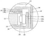
상기 하부커버(140)는 반사판(136)의 하부에 위치하는 밑면과 상기 도광판(135)의 측면 및 LED기판(132)의 후면을 고정시키는 벽면으로 이루어지며, 상기 LED기판(132)의 배면과 하부커버(140)의 벽면 사이에는 LED기판(132)에 실장된 LED(134)로부터 발생된 열을 하부커버(140) 측으로 전달하는 제1방열부재(144a)가 배치된다. 상기 제1방열부재(144a)는 LED기판(132)과 하부커버(140)와 부착되어 LED(134)에서 발생된 열을 하부커버(140)로 전달한다.The
또한, 가이드패널(142)은 상면이 액정패널(110)의 광학시트(138)의 가장자리 및 하부커버(140)의 측면을 감싸는 형태로 하부커버(140)와 결합된다. 이때, 상기 LED기판(132)의 배면과 인접하는 가이드패널(142)과 하부커버(140) 사이에는 제2방열부재(144b)가 배치되어, LED(134)로부터 하부커버(140)로 전달된 열을 가이드패널(142)로 전달한다.The
상기 가이드패널(142)의 상면에는 액정패널(110)이 안착되며, 상기 액정패널(110)의 외곽영역을 상부커버(146)가 덮어 씌어 액정패널(110)과 백라이트가 조립된다. 상기 LED기판(132)의 배면과 인접하는 상부커버(146)와 가이드패널(142) 사이에는 제3방열부재(144c)가 배치되어, LED(134)로부터 가이드패널(142)로 전달 된 열을 상부커버(146)로 전달한다.A
상기와 같은 하부커버(140), 가이드패널(142), 상부커버(146)의 결합구조 및 제1-3방열부재(144a-144c)의 구조를 도 4를 참조하여 더욱 자세히 설명한다.The coupling structure of the
도 4에 도시된 바와 같이, LED기판(132)이 정면에는 복수의 LED(134)가 실장되어 도광판(1350의 측면과 대향하며, 그 배면에는 하부커버(140), 가이드패널(142) 및 상부커버(146)가 차례로 배치된다. 상기 LED기판(132)의 배면과 하부커버(140) 사이, 하부커버(140)와 가이드패널(142) 사이 및 가이드패널(142)과 상부커버(146) 사이에는 제1-3방열부재(144a,144b,144c)가 배치된다.4, a plurality of
도 5는 상기 제1-3방열부재(144a,144b,144c)의 구조를 나타내는 도면이다. 상기 제1-3방열부재(144a,144b,144c)은 동일한 구조로 이루어져 있으므로, 이하에서는 제1방열부재(144a)만을 설명하도록 한다.5 is a view showing a structure of the first to
도 5에 도시된 바와 같이, 제1방열부재(144a)는 제1 및 제2절연층(147a,148a) 및 상기 제1절연층(147a)와 제2절연층(148a) 사이에 형성된 열전도층(149a)으로 이루어진다. 상기 제1 및 제2절연층(147a,148a)은 각각 LED기판(132)과 하부커버(140)와 접촉하는 층으로서, 전기적인 절연특성을 갖기 때문에, 상기 LED기판(132)과 하부커버(140)가 전기적으로 접속되는 것을 방지한다. 상기 열전도층(149a)은 열전도율이 높기 때문에, LED기판(132)의 열을 하부커버(140)로 효과적으로 전달한다.5, the first
상기 제1절연층(147a) 및 제2절연층(148a)은 전기적인 절연성이 좋고 탄성이 있는 실리콘계 고무 등으로 이루어지며, 열전도층(149a)은 폴리이미드나 폴리아미 드와 같은 유기물질에 산화알루미늄 분말이나 붕소질화물(Boron Nitride) 분말이 혼합된 물질로 이루어진다. 또한, 상기 열전도층(149a)은 유리섬유(fiberglass)가 첨가된 방열세라믹으로 형성될 수도 있다.The first insulating
상기와 같은 구성의 제1-3방열부재(144a,144b,144c)의 열전도율은 약 0.7-0.9×10⁻⁴W/mm℃로서, LED기판(132)과 하부커버(140) 사이, 하부커버(140)와 가이드패널(142) 사이 및 가이드패널(142)과 상부커버(146) 사이에 배치되어 열을 외부로 배출한다. 즉, 제1-3방열부재(144a,144b,144c)의 열전도율이 공기의 열전도율(5.0×10⁻⁶W/mm℃) 보다 훨씬 크기 때문에, LED기판(132)과 하부커버(140) 사이, 하부커버(140)와 가이드패널(142) 사이 및 가이드패널(142)과 상부커버(146) 사이에 공기층이 형성된 종래 구조에 비해 외부로 열을 원활하게 배출한다. 또한, 제1-3방열부재(144a,144b,144c)의 제1절연층(147a)와 제2절연층(148a)은 탄성을 갖고 있기 때문에, 하부커버(140)와 가이드패널(142) 및 상부커버(146)를 조립할 때 LED기판(132)과 하부커버(140) 사이, 하부커버(140)와 가이드패널(142) 사이 및 가이드패널(142)과 상부커버(146) 사이에 배치된 제1-3방열부재(144a,144b,144c)가 각각 LED기판(132), 하부커버(140), 가이드패널(142), 상부커버(146)와 밀착되므로, LED기판(132)과 하부커버(140) 사이, 하부커버(140)와 가이드패널(142) 사이 및 가이드패널(142)과 상부커버(146) 사이에는 공기층이 형성되지 않으므로, LED(134)로부터 발생한 광이 원활하게 외부로 배출되는 것이다.The thermal conductivities of the first to
한편, 도면에서는 제1-3방열부재(144a,144b,144c)는 LED기판(132)에 실장된 LED(134)와 정렬되어 배치되지만, LED기판(132)과 정렬되지 않을 수도 있다. 그러나, 실질적으로 LED(134)이 배치되지 않은 영역은 LED(134)의 광에 의한 온도상승이 미미하므로 비용과 공정 등의 단순화를 위해서는 이 영역에는 상기 제1-3방열부재(144a,144b,144c)를 설치하지 않는 것이 바람직할 것이다.Although the first to
도 6은 본 발명의 다른 실시예에 따른 액정표시소자의 구조를 나타내는 도면이고, 도 7는 도 6의 C영역 확대단면도이다. 이때, 도 3에 도시된 실시예와 동일한 구조에 대해서는 설명을 생략하고 다른 구조에 대해서만 설명한다.6 is a view illustrating the structure of a liquid crystal display device according to another embodiment of the present invention, and FIG. 7 is an enlarged cross-sectional view of a region C of FIG. At this time, description of the same structure as the embodiment shown in Fig. 3 will be omitted and only the other structure will be described.
도 6 및 도 7에 도시된 바와 같이, 본 실시예에서는 제1방열부재(244a)가 LED기판(232)과 하부커버(240) 사이에 배치되고 제2방열부재(244b)는 하부커버(240)와 상부커버(246) 사이에 배치된다. 즉, 본 실시예에서는 하부커버(240)와 상부커버(246) 사이의 가이드패널(242)이 일부 제거되고, 제거된 영역에 제2방열부재(244b)가 배치되는 것이다. 이와 같이, 제2방열부재(244b)를 하부커버(240)와 상부커버(246) 사이에 배치함에 따라 LED(234)에서 발생한 열이 LED기판(232), 제1방열부재(244a), 하부커버(240), 제2방열부재(244b) 및 상부커버(246)를 거쳐 외부로 배출된다. 이때, 상기 제1방열부재(244a) 및 제2방열부재(244b)는 LED(234)와 정렬되어 있다. 즉, LED(234)가 실장된 영역에 대응하는 위치에 배치되어 LED(234)로부터 발생하는 열을 용이하게 배출할 수 있게 된다.6 and 7, in this embodiment, the first
이러한 구조의 액정표시소자에서는 도 3에 도시된 실시예의 액정표시소자에 비해 열배출통로에 가이드패널(246)이 제거되고 방열부재의 갯수가 감소하는 반면에, 제2방열부재(244b)의 두께가 증가하였다. 상술한 바와 같이, 방열부재의 열전 도율을 약 0.7-0.9×10⁻⁴W/mm℃이므로, 가이드패널(242)의 열전도율에 비해서는 매우 작다. 그러나, 도 3에 도시된 구조의 액정표시소자에서는 3개의 방열부재가 구비되어 이들이 각각 LED기판, 하부커버, 가이드패널, 상부커버와 접촉하는데 반해, 이 실시예에서는 2개의 방열부재(244a,244b)가 구비되어 LED기판(232), 하부커버(240) 및 상부커버(246)와만 접촉하므로, 방열부재가 접촉하는 부품의 수가 감소하게 된다.3, the
물론, 방열부재(244a,244b)는 탄성을 갖고 있기 때문에, 방열부재(244a,244b)가 LED기판(232)과 하부커버(240) 및 상부커버(246)에 밀착되어 방열부재(244a,244b)와 LED기판(232), 하부커버(240), 상부커버(246) 사이에는 공기층이 존재하지 않는다. 따라서, 이 영역에서 열전도가 전달되지는 않지만, 이 경우에도 서로 다른 열전도율을 갖는 방열부재(244a,244b)와 LED기판(232), 하부커버(240), 상부커버(246) 사이에는 계면이 불연속적이기 때문에 열의 전달이 원활하게 되지 않게 되어 외부로의 열의 배출이 원활하지 않게 된다.Of course, since the
결국, 이 실시예에서는 도 3에 도시된 구조의 액정표시소자보다 불연속적인 계면을 감소시킴으로써 열을 외부로 원활하게 배출될 수 있도록 하여 LED(234)에서 발생된 열에 의해 상승된 액정표시소자의 온도를 하강시킨다.3, the heat can be smoothly discharged to the outside, and the temperature of the liquid crystal display element raised by the heat generated by the
이 실시예에 따르면, 종래 액정표시소자에서 LED의 발열에 의해 액정표시소자가 약 75.1℃까지 상승하는데 반해, 본 실시예의 구조에서는 액정표시소자가 약 71.4℃까지만 상승하므로, 종래에 비해 3.7℃의 온도가 하강하게 된다. 이러한 온 도의 하강에 의해 LED가 열화되는 정도가 저하되므로, LED의 수명을 증가시킬 수 있게 된다.According to this embodiment, the liquid crystal display element of the conventional liquid crystal display element is raised up to about 75.1 DEG C by the heat of the LED, whereas the liquid crystal display element of the present embodiment is raised to about 71.4 DEG C, The temperature is lowered. The lowering of the temperature reduces the degree of deterioration of the LED, so that the lifetime of the LED can be increased.
또한, 이 정도의 온도하강은 LED의 약 5mmA의 전류값에 해당하므로, 종래와 본 실시예의 액정표시소자를 동일한 온도를 유지한다고 가정할 때, 본 실시예의 액정표시소자에 배치된 LED에 약 5mmA가 높은 전류를 인가할 수 있게 되므로, 종래에 비해 액정표시소자의 휘도를 약 6% 향상시킬 수 있게 된다.Assuming that the liquid crystal display element of the present embodiment maintains the same temperature, the temperature of this degree of decrease corresponds to a current value of about 5 mmA of the LED, It is possible to increase the luminance of the liquid crystal display element by about 6% as compared with the conventional art.
한편, 이 실시예에서는 LED(234)에 대응하는 영역의 가이드패널(242) 일부가 제거되어 해당 영역에만 제2방열부재(244b)가 배치되어 있지만, 도 8에 도시된 바와 같이, LED(234)가 배치되는 도광판(235) 측면의 가이드패널(242) 전체를 제거한 후, 해당 영역에 제2방열부재(244b)를 배치할 수도 있다. 이 경우 넓은 면적으로 제2방열부재(244b)가 배치되므로 열의 배출은 용이하지만, 도광판(235)의 측면의 가이드패널(242)의 일부만 제거하는 경우에는 액정패널(210)과 백라이트를 좀더 단단하게 조립할 수 있다는 장점이 있다.In this embodiment, a portion of the
결론적으로, 액정표시소자의 크기 등에 따라 도광판(235)의 측면의 가이드패널(242)의 일부 또는 전부를 제거하고 해당 영역에 제2방열부재(244b)를 배치하는 것이다.Consequently, part or all of the
상술한 바와 같이, 본 발명에서는 LED가 실장되는 LED기판과 상기 LED기판의 배면에 배치되는 하부커버, 가이드패널, 상부커버 사이에 방열부재를 배치함으로써 LED에서 발생하는 열을 외부로 용이하게 방출함으로써 LED의 수명을 향상시키고 액정표시소자의 온도를 하강시켜 액정표시소자의 불량을 방지할 수 있게 된다.As described above, in the present invention, the heat generating member is disposed between the LED substrate on which the LED is mounted and the lower cover, the guide panel, and the upper cover disposed on the back surface of the LED substrate, It is possible to improve the lifetime of the LED and lower the temperature of the liquid crystal display element, thereby preventing defects of the liquid crystal display element.
한편, 상술한 상세한 설명에서는 특정한 구조로서 본 발명을 기술하고 있지만, 본 발명이 이러한 특정 구조에만 한정되는 것은 아니다. 예를 들어, 상세한 설명에서는 LED에서 발생하는 열을 방출하는 방열부 재로서 특정한 재질의 방열부재만을 개시했지만, 공기보다 열전도율이 좋고 하부커버나 상부커버와 같은 금속의 계면특성이 좋아서 계면에 공기층을 형성하지 않는 재질이라도 어떠한 재질의 방열부재를 사용할 수 있을 것이다.While the present invention has been described in detail in the above detailed description, the present invention is not limited to this specific structure. For example, in the detailed description, only a heat radiation member of a specific material is disclosed as a heat radiation member for emitting heat generated from an LED. However, since the thermal conductivity is better than that of air and the interface characteristics of the metal such as the lower cover and the upper cover are good, A heat dissipating member of any material may be used even if it is not formed.
또한, 도면에서는 LED기판이 도광판의 일측에만 형성되어 있지만, 상기 LED기판이 도광판의 양측면 또는 3면이나 4면에 형성될 수도 있을 것이다. 이 경우, 방열부재는 LED기판이 배치되는 영역에도 형성되어야 하므로, 도광판의 양측면 또는 3면이나 4면에 대응하는 LED기판과 하부커버 사이, 하부커버와 가이드패널 사이, 가이드패널과 상부커버 사이에 방열부재가 배치된다. 또한, 상술한 상세한 설명에서는 광원으로서 LED만이 개시되어 있지만, 형광램프나 다른 램프들이 사용될 수도 있을 것이다.In addition, although the LED substrate is formed only on one side of the light guide plate in the drawing, the LED substrate may be formed on both sides or three or four sides of the light guide plate. In this case, since the heat radiating member must be formed in the area where the LED substrate is disposed, it is required to be provided between the LED substrate and the lower cover corresponding to both sides or three or four sides of the light guide plate, between the lower cover and the guide panel, A heat radiation member is disposed. Further, in the above description, only the LED is disclosed as a light source, but a fluorescent lamp or other lamps may be used.
다시 말해서, 별도의 방열부재를 설치하여 광원에서 발생하는 열을 효과적으로 배출할 수만 있다면, 본 발명의 다른 예나 변형예는 본 발명의 기본적인 개념을 이용한 액정표시소자는 본 발명이 속하는 기술분야에 종사하는 사람이라면 누구나 용이하게 창안할 수 있을 것이다.In other words, if another heat dissipating member is provided to effectively dissipate the heat generated in the light source, the liquid crystal display device using the basic concept of the present invention may be applied to other technical fields of the present invention Anyone can easily invent it.
도 1은 종래 액정표시소자의 구조를 나타내는 단면도.1 is a sectional view showing the structure of a conventional liquid crystal display device;
도 2는 도 1의 A영역 확대 단면도.2 is an enlarged cross-sectional view of region A of Fig.
도 3은 본 발명의 일실시예에 따른 액정표시소자의 구조를 나타내는 단면도.3 is a cross-sectional view illustrating a structure of a liquid crystal display device according to an embodiment of the present invention.
도 4는 도 3의 B영역 확대 단면도.4 is an enlarged cross-sectional view of region B of Fig. 3;
도 5는 본 발명에 따른 방열부재의 구조를 나타내는 도면.5 is a view showing a structure of a heat radiation member according to the present invention.
도 6은 본 발명의 다른 실시예에 따른 액정표시소자의 구조를 나타내는 단면도.6 is a cross-sectional view illustrating a structure of a liquid crystal display device according to another embodiment of the present invention.
도 7은 도 6의 C영역 확대 단면도.7 is an enlarged cross-sectional view of the region C of Fig. 6;
도 8은 본 발명의 또 다른 실시예에 따른 확대 단면도.8 is an enlarged cross-sectional view according to another embodiment of the present invention.
Claims (12)
Translated fromKoreanPriority Applications (1)
| Application Number | Priority Date | Filing Date | Title |
|---|---|---|---|
| KR1020090113483AKR101667630B1 (en) | 2009-11-23 | 2009-11-23 | Liquid crystal display device having good efficience of heat rediation therefrom |
Applications Claiming Priority (1)
| Application Number | Priority Date | Filing Date | Title |
|---|---|---|---|
| KR1020090113483AKR101667630B1 (en) | 2009-11-23 | 2009-11-23 | Liquid crystal display device having good efficience of heat rediation therefrom |
Publications (2)
| Publication Number | Publication Date |
|---|---|
| KR20110056966A KR20110056966A (en) | 2011-05-31 |
| KR101667630B1true KR101667630B1 (en) | 2016-10-19 |
Family
ID=44365252
Family Applications (1)
| Application Number | Title | Priority Date | Filing Date |
|---|---|---|---|
| KR1020090113483AExpired - Fee RelatedKR101667630B1 (en) | 2009-11-23 | 2009-11-23 | Liquid crystal display device having good efficience of heat rediation therefrom |
Country Status (1)
| Country | Link |
|---|---|
| KR (1) | KR101667630B1 (en) |
Cited By (2)
| Publication number | Priority date | Publication date | Assignee | Title |
|---|---|---|---|---|
| EP4123247A1 (en) | 2021-07-21 | 2023-01-25 | LG Electronics Inc. | Door assembly, and refrigerator and home appliance including same |
| KR20230014600A (en) | 2021-07-21 | 2023-01-30 | 엘지전자 주식회사 | Door assembly, refrigerator and home applice including the same |
Families Citing this family (9)
| Publication number | Priority date | Publication date | Assignee | Title |
|---|---|---|---|---|
| CN102588849B (en)* | 2012-03-15 | 2016-07-06 | 深圳市华星光电技术有限公司 | A kind of backlight module and liquid crystal indicator |
| US9658659B2 (en) | 2013-01-10 | 2017-05-23 | Lg Electronics Inc. | Display device |
| KR102148718B1 (en)* | 2013-12-18 | 2020-08-27 | 삼성전자주식회사 | Display device |
| KR20160034510A (en) | 2014-09-19 | 2016-03-30 | 삼성디스플레이 주식회사 | Illumination device and display device including the same |
| CN104914619B (en)* | 2015-05-25 | 2018-04-27 | 武汉华星光电技术有限公司 | Backlight module and display device |
| KR102377116B1 (en)* | 2015-06-29 | 2022-03-22 | 엘지디스플레이 주식회사 | Circuit Device Emitting Heat and Backlight Unit Comprising Thereof |
| CN109270723B (en)* | 2018-10-26 | 2025-04-18 | 蚌埠国显科技有限公司 | A new type of liquid crystal display module |
| CN109283743A (en)* | 2018-10-26 | 2019-01-29 | 蚌埠国显科技有限公司 | A liquid crystal display module |
| CN116592319A (en)* | 2023-04-28 | 2023-08-15 | 惠科股份有限公司 | Backlight module and display device |
Citations (2)
| Publication number | Priority date | Publication date | Assignee | Title |
|---|---|---|---|---|
| JP2003168882A (en)* | 2001-11-30 | 2003-06-13 | Sony Corp | Heat conductive sheet |
| JP2005024740A (en)* | 2003-06-30 | 2005-01-27 | Optrex Corp | Liquid crystal display device |
Family Cites Families (2)
| Publication number | Priority date | Publication date | Assignee | Title |
|---|---|---|---|---|
| KR101303892B1 (en)* | 2006-11-03 | 2013-09-05 | 삼성디스플레이 주식회사 | Backlight assembly and liquid crystal display having the same |
| JP5135908B2 (en)* | 2007-06-20 | 2013-02-06 | 三菱電機株式会社 | Display device and liquid crystal display device |
- 2009
- 2009-11-23KRKR1020090113483Apatent/KR101667630B1/ennot_activeExpired - Fee Related
Patent Citations (2)
| Publication number | Priority date | Publication date | Assignee | Title |
|---|---|---|---|---|
| JP2003168882A (en)* | 2001-11-30 | 2003-06-13 | Sony Corp | Heat conductive sheet |
| JP2005024740A (en)* | 2003-06-30 | 2005-01-27 | Optrex Corp | Liquid crystal display device |
Cited By (3)
| Publication number | Priority date | Publication date | Assignee | Title |
|---|---|---|---|---|
| EP4123247A1 (en) | 2021-07-21 | 2023-01-25 | LG Electronics Inc. | Door assembly, and refrigerator and home appliance including same |
| KR20230014600A (en) | 2021-07-21 | 2023-01-30 | 엘지전자 주식회사 | Door assembly, refrigerator and home applice including the same |
| EP4607125A2 (en) | 2021-07-21 | 2025-08-27 | LG Electronics Inc. | Door assembly |
Also Published As
| Publication number | Publication date |
|---|---|
| KR20110056966A (en) | 2011-05-31 |
Similar Documents
| Publication | Publication Date | Title |
|---|---|---|
| KR101667630B1 (en) | Liquid crystal display device having good efficience of heat rediation therefrom | |
| CN101770095B (en) | Liquid crystal display device | |
| KR101529556B1 (en) | Liquid crystal display device having good heat radiating function | |
| KR101255833B1 (en) | Liquid crystal display device | |
| CN103176303B (en) | Display module and the display device with the display module | |
| KR101096759B1 (en) | Backlight assembly and liquid crystal display using the same | |
| KR101214945B1 (en) | Backlight assembly and display device using the same | |
| KR102108214B1 (en) | Light emitting diode assembly and liquid crystal display device having the same | |
| KR101774277B1 (en) | Liquid crystal display device | |
| CN102346332A (en) | Liquid crystal display device with backlight unit | |
| CN101194205A (en) | Liquid crystal display device | |
| KR20160048980A (en) | Backlight module and liquid crystal display module using same | |
| CN101762908A (en) | Liquid crystal display device | |
| KR101513160B1 (en) | Liquid crystal display device having heat radiation sheet | |
| KR101792104B1 (en) | Light guide plate and liquid crystal display device having thereof | |
| KR101796553B1 (en) | Liquid crystal display device | |
| KR101309348B1 (en) | Backlight unit having the same and liquid crystal display divice | |
| KR20120072958A (en) | Back light and liquid crystal display device having thereof | |
| KR101687783B1 (en) | Liquid crystal display device | |
| KR102192957B1 (en) | Back light having light emitting device array | |
| KR101252880B1 (en) | Liquid crystal display divice | |
| KR102218227B1 (en) | Back light and liquid crystal display including the same | |
| KR101920772B1 (en) | Back light and liquid crystal display device having thereof | |
| KR200446930Y1 (en) | Backlight Assembly and Liquid Crystal Display Using Same | |
| KR20120012612A (en) | LCD Display |
Legal Events
| Date | Code | Title | Description |
|---|---|---|---|
| PA0109 | Patent application | St.27 status event code:A-0-1-A10-A12-nap-PA0109 | |
| R18-X000 | Changes to party contact information recorded | St.27 status event code:A-3-3-R10-R18-oth-X000 | |
| PG1501 | Laying open of application | St.27 status event code:A-1-1-Q10-Q12-nap-PG1501 | |
| R18-X000 | Changes to party contact information recorded | St.27 status event code:A-3-3-R10-R18-oth-X000 | |
| R18-X000 | Changes to party contact information recorded | St.27 status event code:A-3-3-R10-R18-oth-X000 | |
| A201 | Request for examination | ||
| PA0201 | Request for examination | St.27 status event code:A-1-2-D10-D11-exm-PA0201 | |
| E902 | Notification of reason for refusal | ||
| PE0902 | Notice of grounds for rejection | St.27 status event code:A-1-2-D10-D21-exm-PE0902 | |
| AMND | Amendment | ||
| E13-X000 | Pre-grant limitation requested | St.27 status event code:A-2-3-E10-E13-lim-X000 | |
| P11-X000 | Amendment of application requested | St.27 status event code:A-2-2-P10-P11-nap-X000 | |
| P13-X000 | Application amended | St.27 status event code:A-2-2-P10-P13-nap-X000 | |
| E601 | Decision to refuse application | ||
| PE0601 | Decision on rejection of patent | St.27 status event code:N-2-6-B10-B15-exm-PE0601 | |
| AMND | Amendment | ||
| P11-X000 | Amendment of application requested | St.27 status event code:A-2-2-P10-P11-nap-X000 | |
| P13-X000 | Application amended | St.27 status event code:A-2-2-P10-P13-nap-X000 | |
| PX0901 | Re-examination | St.27 status event code:A-2-3-E10-E12-rex-PX0901 | |
| PX0701 | Decision of registration after re-examination | St.27 status event code:A-3-4-F10-F13-rex-PX0701 | |
| X701 | Decision to grant (after re-examination) | ||
| GRNT | Written decision to grant | ||
| PR0701 | Registration of establishment | St.27 status event code:A-2-4-F10-F11-exm-PR0701 | |
| PR1002 | Payment of registration fee | St.27 status event code:A-2-2-U10-U11-oth-PR1002 Fee payment year number:1 | |
| PG1601 | Publication of registration | St.27 status event code:A-4-4-Q10-Q13-nap-PG1601 | |
| PR1001 | Payment of annual fee | St.27 status event code:A-4-4-U10-U11-oth-PR1001 Fee payment year number:4 | |
| PR1001 | Payment of annual fee | St.27 status event code:A-4-4-U10-U11-oth-PR1001 Fee payment year number:5 | |
| PC1903 | Unpaid annual fee | St.27 status event code:A-4-4-U10-U13-oth-PC1903 Not in force date:20211014 Payment event data comment text:Termination Category : DEFAULT_OF_REGISTRATION_FEE | |
| PC1903 | Unpaid annual fee | St.27 status event code:N-4-6-H10-H13-oth-PC1903 Ip right cessation event data comment text:Termination Category : DEFAULT_OF_REGISTRATION_FEE Not in force date:20211014 |