KR101666836B1 - Growth technique for phosphor-free white light emitting diode - Google Patents
Growth technique for phosphor-free white light emitting diodeDownload PDFInfo
- Publication number
- KR101666836B1 KR101666836B1KR1020150117534AKR20150117534AKR101666836B1KR 101666836 B1KR101666836 B1KR 101666836B1KR 1020150117534 AKR1020150117534 AKR 1020150117534AKR 20150117534 AKR20150117534 AKR 20150117534AKR 101666836 B1KR101666836 B1KR 101666836B1
- Authority
- KR
- South Korea
- Prior art keywords
- layer
- nitride semiconductor
- semiconductor layer
- ingan
- porous
- Prior art date
- Legal status (The legal status is an assumption and is not a legal conclusion. Google has not performed a legal analysis and makes no representation as to the accuracy of the status listed.)
- Active
Links
- 238000000034methodMethods0.000titleclaimsabstractdescription21
- 239000004065semiconductorSubstances0.000claimsabstractdescription67
- 150000004767nitridesChemical class0.000claimsabstractdescription61
- 229910052738indiumInorganic materials0.000claimsabstractdescription13
- APFVFJFRJDLVQX-UHFFFAOYSA-Nindium atomChemical compound[In]APFVFJFRJDLVQX-UHFFFAOYSA-N0.000claimsabstractdescription13
- 238000005229chemical vapour depositionMethods0.000claimsdescription5
- 238000011065in-situ storageMethods0.000claimsdescription5
- 229910052751metalInorganic materials0.000claimsdescription5
- 239000002184metalSubstances0.000claimsdescription5
- 238000004519manufacturing processMethods0.000abstractdescription11
- OAICVXFJPJFONN-UHFFFAOYSA-NPhosphorusChemical compound[P]OAICVXFJPJFONN-UHFFFAOYSA-N0.000abstractdescription9
- 239000000463materialSubstances0.000abstractdescription3
- 230000001788irregularEffects0.000abstract1
- 239000010410layerSubstances0.000description172
- 229910004205SiNXInorganic materials0.000description18
- 230000007547defectEffects0.000description10
- 239000000758substrateSubstances0.000description9
- 238000004458analytical methodMethods0.000description4
- 238000005401electroluminescenceMethods0.000description4
- 238000000206photolithographyMethods0.000description3
- 239000002096quantum dotSubstances0.000description3
- 238000001350scanning transmission electron microscopyMethods0.000description3
- 238000001228spectrumMethods0.000description3
- 238000004627transmission electron microscopyMethods0.000description3
- 239000003086colorantSubstances0.000description2
- 239000013078crystalSubstances0.000description2
- 230000000694effectsEffects0.000description2
- 238000012986modificationMethods0.000description2
- 230000004048modificationEffects0.000description2
- 230000003287optical effectEffects0.000description2
- 238000000623plasma-assisted chemical vapour depositionMethods0.000description2
- 229910010093LiAlOInorganic materials0.000description1
- 229910020068MgAlInorganic materials0.000description1
- 229910004298SiO 2Inorganic materials0.000description1
- BLRPTPMANUNPDV-UHFFFAOYSA-NSilaneChemical compound[SiH4]BLRPTPMANUNPDV-UHFFFAOYSA-N0.000description1
- 230000002411adverseEffects0.000description1
- 230000004888barrier functionEffects0.000description1
- 230000015572biosynthetic processEffects0.000description1
- 239000000470constituentSubstances0.000description1
- 238000007796conventional methodMethods0.000description1
- 230000000593degrading effectEffects0.000description1
- 238000009826distributionMethods0.000description1
- 230000005684electric fieldEffects0.000description1
- 238000010894electron beam technologyMethods0.000description1
- 239000010408filmSubstances0.000description1
- 238000005286illuminationMethods0.000description1
- 238000001459lithographyMethods0.000description1
- 238000004020luminiscence typeMethods0.000description1
- 239000002105nanoparticleSubstances0.000description1
- TWNQGVIAIRXVLR-UHFFFAOYSA-Noxo(oxoalumanyloxy)alumaneChemical compoundO=[Al]O[Al]=OTWNQGVIAIRXVLR-UHFFFAOYSA-N0.000description1
- 238000005424photoluminescenceMethods0.000description1
- 230000006798recombinationEffects0.000description1
- 238000005215recombinationMethods0.000description1
- 229910052594sapphireInorganic materials0.000description1
- 239000010980sapphireSubstances0.000description1
- 239000002356single layerSubstances0.000description1
- 239000000126substanceSubstances0.000description1
- 239000010409thin filmSubstances0.000description1
Images


Classifications
- H01L33/0075—
- H01L21/205—
- H01L33/007—
- H—ELECTRICITY
- H01—ELECTRIC ELEMENTS
- H01L—SEMICONDUCTOR DEVICES NOT COVERED BY CLASS H10
- H01L2924/00—Indexing scheme for arrangements or methods for connecting or disconnecting semiconductor or solid-state bodies as covered by H01L24/00
- H01L2924/10—Details of semiconductor or other solid state devices to be connected
- H01L2924/11—Device type
- H01L2924/12—Passive devices, e.g. 2 terminal devices
- H01L2924/1204—Optical Diode
- H01L2924/12041—LED
Landscapes
- Led Devices (AREA)
Abstract
Translated fromKorean
Description
Translated fromKorean본 발명은 형광체 없는 백색 발광다이오드 및 그 제조 방법에 관한 발명으로서, 보다 구체적으로는 다공성 나노 마스크층을 이용하여 활성층(active region)을 다중면(multi-facet) 구조로 형성시키고, 그에 따라 활성층 내 각 위치마다 인듐(In)층의 두께 및/또는 인듐의 농도가 달라지는 것을 이용하여 형광체를 이용하지 않고 백색광을 발광하는 백색 발광다이오드를 제조할 수 있는 방법에 관한 것이다.The present invention relates to a phosphor-free white light emitting diode and a method of manufacturing the same. More specifically, the present invention relates to a white light emitting diode without a phosphor and a method of manufacturing the same, and more particularly to a multi- And a method of manufacturing a white light emitting diode which emits white light without using a phosphor by using the fact that the thickness of the indium (In) layer and / or the concentration of indium is varied at each position.
발광다이오드(LED: light-emitting diode)는 P-N접합 다이오드의 일종으로, 순방향으로 전압이 걸릴 때 단파장광(monochromatic light)이 방출되는 현상인 전기발광효과(electroluminescence)를 이용한 반도체 소자이다. 발광다이오드의 동작은 양극과 음극으로 표현되는 2개의 전극에 전압을 인가하고, 전압 인가에 따른 전류의 공급에 의해 발광동작이 수행되는 메커니즘이다. 특히, 다중양자우물 구조가 형성된 활성층에는 N형 반도체층과 P형 반도체층이 상하부에 접촉된다. N형 반도체층은 활성층에 전자를 공급하고, P형 반도체층은 활성층(active region)에 정공을 공급한다. 다중양자우물 구조에 투입된 전자 및 정공은 양자구속효과에 의해 우물층 내부에 정의되고, 재결합에 의해 발광동작이 수행된다.A light-emitting diode (LED) is a type of P-N junction diode, and is a semiconductor device using electroluminescence, which is a phenomenon in which monochromatic light is emitted when voltage is applied in the forward direction. The operation of the light emitting diode is a mechanism in which a voltage is applied to two electrodes represented by an anode and a cathode, and a light emission operation is performed by supplying a current according to a voltage application. Particularly, in the active layer in which the multiple quantum well structure is formed, the N-type semiconductor layer and the P-type semiconductor layer are in contact with the upper and lower portions. The N-type semiconductor layer supplies electrons to the active layer, and the P-type semiconductor layer supplies holes to the active region. Electrons and holes injected into the multiple quantum well structure are defined inside the well layer by the quantum confinement effect, and the light emitting operation is performed by recombination.
최근, 질화물 반도체를 이용한 발광다이오드를 백색 광원으로 활용하여 이를 키패드, 백라이트, 신호등, 공항활주로의 안내등, 조명등 등으로 다양한 분야에서 활용하고 있다.In recent years, light emitting diodes using nitride semiconductors have been utilized as white light sources and used in various fields such as keypads, backlights, signal lamps, guidance of airport runways, and illumination lights.
도 1에서 볼 수 있는 바와 같이 종래에는 활성층의 청색광이 형광체에 조사되고, 그로 인해 상기 형광체로부터 황색광이 발광되도록 하여 상기 활성층에 의한 청색광과 상기 형광체에 의한 황색광을 중첩시켜 백색광이 발광되도록 하는 방식으로 백색 발광다이오드를 구현하였고, 현재 상용화되어 널리 이용되고 있다. 그러나 형광체는 열에 약해 쉽게 열화되는 문제점이 있어, 이를 보완하기 위하여 형광체를 포함하지 않는 백색 발광다이오드 연구가 진행되었고, 도 2에서 볼 수 있는 바와 같이 별도의 형광체를 이용하지 않고 질화물 반도체를 다중면(multi-facet) 구조로 성장시켜 그로부터 다중색이 발광되고, 상기 다중색의 중첩으로 백색광이 방출되도록 하는 방식으로 진화하였다.As shown in FIG. 1, conventionally, the blue light of the active layer is irradiated to the phosphor, thereby emitting yellow light from the phosphor, thereby superimposing the blue light by the active layer and the yellow light by the phosphor to emit white light White light emitting diode (LED) has been implemented and is now widely used. However, there is a problem that the phosphor is easily deteriorated due to heat. To overcome this problem, a white light emitting diode (LED) without a phosphor has been studied. As shown in FIG. 2, multi-facet structure to emit multi-colors, and to emit white light by overlapping the multiple colors.
그러나, 종래 다중면(multi-facet) 구조를 이용하는 방법의 경우에도 SiO2층을 PECVD 등의 공정을 통해 증착시킨 후 다시 포토리소그래피 등의 별도 공정을 통해 다중면(multi-facet) 구조로 질화물 반도체층을 형성시켜야 하는 제조상의 번거로움이 있었다.However, in the case of a conventional method using a multi-facet structure, the SiO 2 layer is deposited through a process such as PECVD, and then the nitride semiconductor layer is formed in a multi-facet structure through another process such as photolithography. There is a manufacturing cost incurred in forming the film.
본 발명은 상기와 같은 종래 기술의 문제점을 해결하기 위해 창안된 것으로, 본 발명은 MOCVD(Metal Organic Chemical Vapor Deposition)를 이용하여 인시추(in-situ) 방식으로 다공성 나노 마스크층을 형성시키고 그 상부에 질화물 반도체층, 활성층(active region) 등을 다중면(multi-facet) 구조로 형성시킴으로써 포토리소그래피 등의 별도의 공정 없이 백색광을 방출하는 발광다이오드 및 그 제조 방법을 제공하는 것을 목적으로 한다.SUMMARY OF THE INVENTION The present invention has been made to overcome the problems of the prior art as described above, and it is an object of the present invention to provide a method of forming a porous nanomask layer by in-situ method using MOCVD (Metal Organic Chemical Vapor Deposition) A nitride semiconductor layer, an active region, or the like is formed in a multi-facet structure, thereby emitting white light without a separate process such as photolithography, and a manufacturing method thereof.
상기한 과제를 해결하기 위한 본 발명의 한 측면에 따른 형광체 없는 백색 발광다이오드에 있어서,According to an aspect of the present invention, there is provided a phosphorless white light emitting diode,
다공성 나노 마스크층; 상기 다공성 나노 마스크층의 구멍을 통해 성장된 제1 질화물 반도체가 다중면(multi-facet) 구조로 형성되는 제1 질화물 반도체층; 및 상기 제1 질화물 반도체층의 상부에 제2 질화물 반도체가 다중면(multi-facet) 구조로 형성되는 활성층;을 포함할 수 있다.Porous nano-mask layer; A first nitride semiconductor layer in which a first nitride semiconductor grown through a hole of the porous nanomask layer is formed in a multi-facet structure; And an active layer in which a second nitride semiconductor is formed in a multi-facet structure on the first nitride semiconductor layer.
여기서, 상기 다공성 나노 마스크층의 구멍의 크기는 수nm 내지 수백nm인 것을 포함할 수 있다.Here, the size of the hole of the porous nanomask layer may include several nm to several hundreds nm.
또한, 상기 활성층은, 상기 제2 질화물 반도체 및 제3 질화물 반도체가 다중면(multi-facet) 구조로 형성될 수 있다.In addition, the active layer may have a multi-facet structure in which the second and third nitride semiconductors are formed.
또한, 상기 제2 질화물 반도체는, InGaN이고, 상기 InGaN는 상기 제1 질화물 반도체층의 상부에 불균일한 두께로 형성될 수도 있다.In addition, the second nitride semiconductor may be InGaN, and the InGaN may be formed on the first nitride semiconductor layer to have a non-uniform thickness.
또한, 상기 제2 질화물 반도체는, InGaN이고, 상기 InGaN는 상기 제1 질화물 반도체층의 상부에 불균일한 인듐(In) 농도로 형성될 수도 있다.In addition, the second nitride semiconductor may be InGaN, and the InGaN may be formed on the first nitride semiconductor layer in a non-uniform indium (In) concentration.
상기 과제를 해결하기 위한 본 발명의 다른 측면에 따른 형광체 없는 백색 발광다이오드 제조 방법에 있어서,According to another aspect of the present invention, there is provided a method of manufacturing a phosphorless white light emitting diode,
다공성 나노 마스크층을 형성시키는 단계; 상기 다공성 나노 마스크층의 구멍을 통해 제1 질화물 반도체를 성장시켜 다중면(multi-facet) 구조의 제1 질화물 반도체층을 형성시키는 단계; 및 상기 제1 질화물 반도체층의 상부에 제2 질화물 반도체를 성장시켜 다중면(multi-facet) 구조의 활성층을 형성시키는 단계;를 포함할 수 있다.Forming a porous nanomask layer; Growing a first nitride semiconductor through holes in the porous nanomask layer to form a first nitride semiconductor layer having a multi-facet structure; And growing a second nitride semiconductor on the first nitride semiconductor layer to form an active layer having a multi-facet structure.
상기 각 단계는, MOCVD(Metal Organic Chemical Vapor Deposition)를 이용하여 인시추(in-situ) 방식으로 수행될 수 있다.Each of the above steps may be performed in-situ using MOCVD (Metal Organic Chemical Vapor Deposition).
또한, 상기 활성층을 형성시키는 단계는, 상기 제2 질화물 반도체 및 제3 질화물 반도체를 다중면(multi-facet) 구조로 형성될 수 있다.In the forming of the active layer, the second nitride semiconductor and the third nitride semiconductor may be formed in a multi-facet structure.
또한, 상기 제2 질화물 반도체는, InGaN이고, 상기 InGaN는 상기 제1 질화물 반도체층의 상부에 불균일한 두께로 형성될 수도 있다.In addition, the second nitride semiconductor may be InGaN, and the InGaN may be formed on the first nitride semiconductor layer to have a non-uniform thickness.
또한, 상기 제2 질화물 반도체는, InGaN이고, 상기 InGaN는 상기 제1 질화물 반도체층의 상부에 불균일한 인듐(In) 농도로 형성될 수도 있다.In addition, the second nitride semiconductor may be InGaN, and the InGaN may be formed on the first nitride semiconductor layer in a non-uniform indium (In) concentration.
본 발명의 실시예에 따르면, MOCVD(Metal Organic Chemical Vapor Deposition)를 이용하여 인시추(in-situ) 방식으로 전체 공정을 수행하므로 다공성 나노 마스크층, 질화물 반도체층, 활성층 등을 형성시킴에 있어서 포토리소그래피 등의 별도의 공정이 불필요하므로 경제적이다.According to an embodiment of the present invention, since the entire process is performed in-situ using MOCVD (Metal Organic Chemical Vapor Deposition), in forming the porous nano-mask layer, the nitride semiconductor layer, the active layer, A separate process such as lithography is unnecessary, which is economical.
또한, 다공성 나노 마스크층을 이용하여 그 하부 층의 결함을 차단하고, 상기 다공성 나노 마스크층의 구멍을 통해 질화물 반도체층 및 활성층을 다중면(multi-facet) 구조로 형성시킴으로써 형광체를 사용하지 않고도 백색 발광다이오드를 얻을 수 있다.In addition, by using the porous nano-mask layer to block defects in the lower layer and to form the nitride semiconductor layer and the active layer in a multi-facet structure through the holes of the porous nano-mask layer, A light emitting diode can be obtained.
또한, 다중면 구조는 활성층의 면적을 키워 평면 구조의 활성층에 비하여 발광량을 증가시킬 수 있다.In addition, the multi-facet structure can increase the light emitting amount as compared with the active layer having the planar structure by increasing the area of the active layer.
본 발명에 관한 이해를 돕기 위해 상세한 설명의 일부로 포함되는, 첨부도면은 본 발명에 대한 실시예를 제공하고, 상세한 설명과 함께 본 발명의 기술적 사상을 설명한다.
도 1은 종래 형광체를 이용한 백색 발광다이오드의 구조를 도시한 것이다.
도 2는 종래 PECVD 및 포토리소그래피 공정을 이용한 형광체 없는 백색 발광다이오드의 구조를 도시한 것이다.
도 3은 본 발명의 일 실시예에 따른 형광체 없는 백색 발광다이오드의 구조를 도시한 것이다.
도 4는 본 발명의 일 실시예에 따른 형광체 없는 백색 발광다이오드의 제조 과정을 도시한 것이다.
도 5는 본 발명의 일 실시예에 따른 형광체 없는 백색 발광 이종접합구조를 TEM 분석한 것이다.
도 6은 본 발명의 일 실시예에 따른 형광체 없는 백색 발광 이종접합구조를 STEM 분석한 것이다.
도 7은 청색 발광 조건에서 활성층이 평면 구조인 경우 및 다중면 이종접합구조인 경우의 광루미네선스 차이를 도시한 것이다.
도 8은 청색 발광 조건에서 활성층이 평면 구조인 발광다이오드의 경우 및 다중면 구조인 발광다이오드의 경우의 전기루미네선스 차이를 도시한 것이다.BRIEF DESCRIPTION OF THE DRAWINGS The accompanying drawings, which are included to provide a further understanding of the invention and are incorporated in and constitute a part of the specification, illustrate embodiments of the invention and, together with the description, serve to explain the principles of the invention.
FIG. 1 shows a structure of a white light emitting diode using a conventional phosphor.
FIG. 2 illustrates the structure of a phosphor-free white light emitting diode using conventional PECVD and photolithography processes.
FIG. 3 illustrates a structure of a phosphorless white light emitting diode according to an embodiment of the present invention. Referring to FIG.
4 illustrates a process of fabricating a phosphorless white light emitting diode according to an embodiment of the present invention.
FIG. 5 is a TEM analysis of a phosphor-free white light emitting heterogeneous junction structure according to an embodiment of the present invention.
6 is a STEM analysis of a phosphor-free white light emitting heterogeneous junction structure according to an embodiment of the present invention.
FIG. 7 shows the optical luminescence difference in the case where the active layer has a planar structure and the multi-plane heterojunction structure in a blue light emission condition.
FIG. 8 shows the difference in the electroluminescence between the light emitting diode having the planar structure of the active layer and the light emitting diode having the multi-plane structure under the blue light emission condition.
본 발명은 다양한 변환을 가할 수 있고 여러 가지 실시예를 가질 수 있는 바, 이하에서는 특정 실시예들을 첨부된 도면을 기초로 상세히 설명하고자 한다.BRIEF DESCRIPTION OF THE DRAWINGS The present invention is capable of various modifications and various embodiments, and specific embodiments will be described in detail below with reference to the accompanying drawings.
본 발명을 설명함에 있어서 관련된 공지 기술에 대한 구체적인 설명이 본 발명의 요지를 흐릴 수 있다고 판단되는 경우 그 상세한 설명을 생략한다.DETAILED DESCRIPTION OF THE PREFERRED EMBODIMENTS Hereinafter, the present invention will be described in detail with reference to the accompanying drawings.
제1, 제2 등의 용어는 다양한 구성요소들을 설명하는데 사용될 수 있지만, 상기 구성요소들은 상기 용어들에 의해 한정되는 것은 아니며, 상기 용어들은 하나의 구성요소를 다른 구성요소로부터 구별하는 목적으로만 사용된다.The terms first, second, etc. may be used to describe various components, but the components are not limited by the terms, and the terms are used only for the purpose of distinguishing one component from another Is used.
이하에서는, 본 발명에 따른 형광체 없는 백색 발광다이오드 및 그 제작 방법을 예시적인 실시 형태들을 첨부된 도면을 참조하여 상세히 설명한다.Hereinafter, exemplary embodiments of a phosphor-free white light emitting diode and a manufacturing method thereof according to the present invention will be described in detail with reference to the accompanying drawings.
도 3은 본 발명의 일 실시예에 따른 형광체 없는 백색 발광다이오드(300)의 구조를 도시한 것이다.3 illustrates a structure of a phosphorless white
본 발명의 일 실시예에 따른 형광체 없는 백색 발광다이오드(300)는 기판 상부에 순차적으로 n형 질화물 반도체층, 다공성 나노 마스크층, 다중면(multi-facet) 구조의 질화물 반도체층, 다중면 구조의 활성층(active region), p형 질화물 반도체층을 포함하여 형성될 수 있다.A phosphor-free white
보다 구체적으로는, 도 3에서 볼 수 있는 바와 같이 형광체 없는 백색 발광다이오드(300)는 사파이어 기판(310) 상부에 순차적으로 N-GaN층(320), 다공성 SiNx 나노 마스크층(330), 다중면 구조의 GaN층(340), 다중면 구조의 InGaN/GaN 활성층(350), P-GaN층(360)을 포함하여 형성될 수 있다.3, the phosphor-free white
또한, 상기 기판(310)과 상기 N-GaN층(320) 사이에 도핑되지 않은 GaN층(u-GaN층)을 더 포함할 수도 있다. 상기 도핑되지 않은 GaN층(u-GaN층)은 상기 기판(310)과 상기 N-GaN층(320) 사이의 격자 상수 및 열팽창 계수의 차이를 극복하기 위하여 형성하는 것으로, 상기 도핑되지 않은 GaN층(u-GaN층)을 성장시킨 후, 상기 N-GaN층(320)을 성장시키면 N-GaN층(320)의 결정질을 향상시킬 수 있다. 다만, 상기 N-GaN층(320)이 상기 도핑되지 않은 GaN층(u-GaN층) 상에 형성되었다 하더라도 상기 도핑되지 않은 GaN층(u-GaN층) 역시 상기 기판(310)과의 상이한 물리적 특성으로 인해 많은 결함을 내포하고 있으며, 이러한 결함은 상기 도핑되지 않은 GaN층(u-GaN층) 상에 성장시킨 N-GaN층(320)에 그대로 전달되게 된다. 다만, 결함은 이하 설명될 다공성 나노 마스크층에 의하여 어느 정도 차단시킬 수 있다.In addition, a non-doped GaN layer (u-GaN layer) may be further disposed between the
상기 기판(310)은 사파이어(Al2O3) 기판은 물론 질화물 단결정 성장용 기판으로 알려진 다른 공지된 기판을 사용할 수 있다. 예를 들어, SiC, Si, MgAl2O4, MgO, LiAlO2 또는 LiGaO2 등을 포함할 수 있다.The
상기 다공성 SiNx 나노 마스크층(330)은 수nm 내지 수백nm 두께로 형성될 수 있다. 또한, 상기 다공성 SiNx 나노 마스크층(330)은 다수의 구멍을 포함할 수 있으며, SiNx 이외에 MgN를 이용하여 형성될 수도 있다.The porous
상기 다중면 구조의 GaN층(340)은 상기 다공성 SiNx 나노 마스크층(330)의 구멍을 통해 성장 초기에는 독립된 기둥 모양으로 성장하여 소정의 높이 이상에서 서로 결합하여 올록볼록한 다중면 구조를 이룬다.The
상기 활성층(350)은 전자 및 정공이 재결합되어 발광하는 영역으로서, 본 발명에서는 InGaN을 포함하여 형성된다. 상기 활성층(350)을 이루는 물질의 종류에 따라 발광다이오드에서 방출되는 빛의 파장이 결정된다. 상기 활성층은 InxAlyGa1-x-yN(0≤x, 0≤y, x+y≤1)의 우물층과 InxAlyGa1-x-yN (0≤x, 0≤y, x+y≤1)의 장벽층으로 이루어진 단일 양자우물구조 또는 다중 양자우물구조 또는 3차원의 양자점(quantum dot) 구조로 형성될 수 있다. 본 발명에서의 상기 우물층 및 장벽층은 각각 InGaN 및 GaN에 대응된다. 상기 InGaN층 및 GaN층은 각각 수nm 내지 수백nm 범위로 형성될 수 있고, 상기 InGaN층의 인듐(In) 함량은 0.1% ~ 100% 범위일 수 있다. 다만, 인듐(In) 함량이 100%일 경우에는 InGaN층이 아니라 InN층에 해당한다.The
상기 P-GaN층(360)은 상기 활성층(350)의 상부에 단일층으로 형성되고, 두께는 0.1 um 내지 1 um 범위로 형성될 수 있다.The P-
도 4는 본 발명의 일 실시예에 따른 형광체 없는 백색 발광다이오드의 제조 과정을 도시한 것이다.4 illustrates a process of fabricating a phosphorless white light emitting diode according to an embodiment of the present invention.
본 발명의 목적을 달성하기 위한 백색 발광다이오드 제조 과정은 MOCVD(Metal Organic Chemical Vapor Deposition)를 이용하여 인시추(in-situ) 방식으로 수행될 수 있다.In order to achieve the object of the present invention, the process of fabricating a white light emitting diode may be performed in-situ using MOCVD (Metal Organic Chemical Vapor Deposition).
우선 도 4(a)를 참조하면, N-GaN층(320) 상부에 다공성 SiNx 나노 마스크층(330)을 형성시킨다. 이때, MOCVD를 이용함에 있어서 온도/압력/유량/시간 등을 조절하여 상기 다공성 SiNx 나노 마스크층(330)이 복수개의 구멍을 포함할 수 있도록 형성시킨다.Referring to FIG. 4A, a porous SiNx nano-
다만, 상기 다공성 SiNx 나노 마스크층(330)은 N-GaN층 상부에 형성되는 것을 기준으로 설명하였으나 상기 다공성 SiNx 나노 마스크층(330)은 상기 기판(310) 상부 또는 u-GaN층 상부 등에 형성될 수 있고, N-GaN층 상부에 별도의 다른 반도체층이 형성되는 경우에는 상기 다른 반도체층의 상부에 형성될 수도 있다.Although the porous SiNx nano-
상기 다공성 SiNx 나노 마스크층은 MOCVD를 이용하여 온도 500 ~ 1100, 압력 10 ~ 760torr, 유량은 SiH4가스가 0.1 ~ 100sccm, NH3가스가 10 ~ 10000sccm, 시간은 5 ~ 5000초 범위에서 형성될 수 있다.The porous SiNx nano-mask layer may be formed by MOCVD at a temperature of 500 to 1100, a pressure of 10 to 760 torr, a flow rate of SiH4 gas of 0.1 to 100 sccm, NH3 gas of 10 to 10000 sccm, and a duration of 5 to 5000 seconds.
다음으로 도 4(b)를 참조하면, 다공성 SiNx 나노 마스크층(330) 상부에 다중면(multi-facet) 구조의 GaN층(340)을 형성시킬 수 있다.Next, referring to FIG. 4B, a
상기 다중면(multi-facet) 구조의 GaN층(340)는 상기 다공성 SiNx 나노 마스크층(330)의 구멍을 통해 성장하고 SiNx가 증착된 부분은 성장하지 않으므로, 상기 다중면(multi-facet) 구조의 GaN층(340)의 성장 초기에는 나노 크기의 독립한 복수개의 기둥 모양으로 성장하게 된다. 이후에 계속적으로 성장시키면 기둥 모양의 GaN층이 소정의 높이 이상에서 서로 결합하면서 올록볼록한 다중면 구조의 GaN층이 형성된다.The
상기 다공성 SiNx 나노 마스크층(330)의 구멍 크기에 따라 다중면 구조를 이루는 기둥의 너비가 결정된다. 상기 기둥 모양의 GaN층의 너비가 좁을수록 발광다이오드는 상기 N-GaN층(320)의 결함에 의한 영향을 적게 받으며 또한, 상기 활성층(350)의 면적을 키워 발광량을 증대시킬 수 있으며, P-GaN층의 상부를 평평하게 형성시키는데 유리하다.The width of the multi-faceted column is determined by the hole size of the porous
다음으로 도 4(c)를 참조하면, 상기 다중면(multi-facet) 구조의 GaN층(340)의 상부에 다중면(multi-facet) 구조의 활성층(350)을 형성시킬 수 있다.Referring to FIG. 4C, an
상기 활성층(350)은 전자 및 정공이 재결합되어 발광하는 영역으로서, 본 발명에서는 InGaN층 및 GaN층를 포함하여 형성된다. 일반적으로 InGaN층과 GaN층이 순차적으로 적층되며, 단일양자우물구조, 다중양자우물구조 또는 박막형태가 아닌 3차원 구조체를 이루는 양자점 구조 등으로 형성될 수 있다.The
상기 활성층(350)을 이루는 InGaN층 및 GaN층은 각각 온도 500 ~ 990℃, 압력 10 ~ 760torr 범위에서 형성될 수 있으며, 그 두께는 2 ~ 300nm 범위에서 형성될 수 있다.The InGaN layer and the GaN layer constituting the
상기 InGaN층은 상기 다중면 구조의 GaN층(340)의 각 면에서의 표면에너지가 각기 다르므로 불균일한 두께로 형성되며, 상기 InGaN층의 각 위치에 따라 인듐(In)의 함량이 서로 다르게 분포할 수 있다. 상기 InGaN층의 상부에 형성되는 상기 GaN층은 상기 InGaN층과 함께 양자우물구조를 형성하고, 상기 InGaN층을 보호하는 역할을 한다.The InGaN layer has a non-uniform thickness because the surface energy of the
다음으로 도 4(d)를 참조하면, 다중면의 구조로 형성된 활성층(350)을 전자현미경으로 촬영한 것이다.Next, referring to FIG. 4 (d), the
도 4(d)에서 볼 수 있는 바와 같이, 촬영 사진의 가운데의 밝은 부분을 보면 상기 활성층(350)이 올록볼록한 형태의 다중면(multi-facet) 구조로 형성되어 있음을 확인할 수 있다.As can be seen in FIG. 4 (d), it can be seen that the
도 5는 본 발명의 일 실시예에 따른 형광체 없는 백색 발광 이종접합구조(Doublehetero: DH)를 TEM(Transmission Electron Microscopy) 분석한 것이다.FIG. 5 is a TEM (Transmission Electron Microscopy) analysis of a phosphor-free white light emitting heterogeneous junction structure (Doublehetero: DH) according to an embodiment of the present invention.
통상적으로 사파이어 기판 상부에 GaN 등의 질화물 반도체층이 형성될 때 격자 부정합과 구성 원소간의 열팽창 계수 차이에 의한 선 결함, 면 결함 등의 결정 결함이 존재하고, 이러한 결정 결함은 그 위에 재성장되는 질화물 반도체 층에도 영향을 미쳐, 분극장 형성으로 인한 압전 현상(piezoelectric effect)으로 내부 양자효율이 저하되거나 광소자의 신뢰성 등에 악영향을 줄 수 있고, 소자 내의 전류 누설의 원인이 되어 양자효율을 감소시켜 결과적으로 광소자의 성능을 저하시키게 된다. 그러므로 상기 결함의 영향을 줄이는 공정이 필수적으로 요구된다.Generally, when a nitride semiconductor layer such as GaN is formed on a sapphire substrate, crystal defects such as a line defect and a surface defect due to a difference in thermal expansion coefficient between constituent elements exist in the lattice mismatch, Layer, the piezoelectric effect due to the formation of a polarizing field may degrade the internal quantum efficiency, adversely affect the reliability of the optical device, cause current leakage in the device, and decrease the quantum efficiency. As a result, Thereby degrading the performance of the device. Therefore, a process for reducing the influence of the defect is indispensably required.
상기 도 5에서 볼 수 있는 바와 같이 본 발명에서는 결함이 존재하는 층의 상부에 다공성 SiNx 나노 마스크층을 형성시켜 결함을 차단할 수 있다. 또한, 상기 SiNx 나노 마스크층의 구멍을 통해 성장시킨 기둥 모양의 GaN층을 확인할 수 있는데 기둥의 너비가 수nm 내지 수백nm에 불과하므로 상기 도 2에서의 너비가 수십um에 달하는 종래 기술의 다중면 구조에 비하여 결함에 의한 전류 누설 등의 영향이 적다.As shown in FIG. 5, in the present invention, a porous SiNx nano-mask layer may be formed on the defect-existing layer to prevent defects. In addition, the columnar GaN layer grown through the holes of the SiNx nanomask layer can be confirmed. Since the width of the column is only a few nanometers to a few hundreds of nanometers, the prior art multi- The influence of leakage current due to defects is less than that of the structure.
도 6은 본 발명의 일 실시예에 따른 형광체 없는 백색 발광 이종접합구조(Doublehetero: DH)를 STEM(Scanning Transmission Electron Microscopy) 분석한 것이다.6 is a STEM (Scanning Transmission Electron Microscopy) analysis of a phosphor-free white light emitting heterogeneous junction structure (DH) according to an embodiment of the present invention.
도 6(a)는 다중면(multi-facet) 구조의 GaN층(340) 및 활성층(350)을 도시한 것이다. 상기 다공성 SiNx 나노 마스크층(330) 상부에 기둥 모양의 GaN층이 성장하여 다중면(multi-facet) 구조의 GaN층(340)을 형성하고, 상기 다중면 구조의 GaN층의 상부에 다시 활성층(350)이 형성된다.6 (a) shows a
상기 다중면 구조의 GaN층(340) 상부의 각 면에 따라 표면에너지가 달라지게 되므로 상기 다중면 구조의 GaN층(340)의 상부에 형성되는 InGaN층은 균일하게 형성되지 않고 각각의 표면에너지에 따라 상기 InGaN층이 불균일한 두께 및 불균일한 인듐(In)의 농도로 적층될 수 있다.Since the surface energy of the
도 6(b)는 상기 도 6(a)의 P1 내지 P5 위치에서의 각각의 에너지 분포를 도시한 것이다. 상기 P1 내지 P5 위치에 따라 가속 전자빔에 의해서 방출되는 X-선 에너지 스펙트럼을 그래프로 나타낸 것이며, 각 위치에 따라 각기 다른 스펙트럼을 나타내는 것을 확인할 수 있다. 이는 P1 내지 P5의 위치에서의 인듐(In)의 농도가 서로 다름을 의미하고, 나아가 발광다이오드로서 동작 시 상기 InGaN층의 각 위치에 따라 방출하는 빛의 파장이 각기 다름을 의미한다. 이러한 방법으로 본 발명에 따른 발광다이오드는 상기 InGaN층의 각각의 위치에서 방출하는 빛의 파장의 합이 가시광선 전체 영역을 모두 포함할 수 있게 되므로 백색광을 방출할 수 있다.Fig. 6 (b) shows the respective energy distributions at the positions P1 to P5 in Fig. 6 (a). The X-ray energy spectrum emitted by the accelerating electron beam according to the positions of P1 to P5 is a graph, and it can be confirmed that each spectrum shows different spectra depending on each position. This means that the concentrations of indium (In) at the positions P1 to P5 are different from each other. Further, when operating as a light emitting diode, the wavelength of light emitted according to each position of the InGaN layer is different. In this manner, the light emitting diode according to the present invention can emit white light because the sum of the wavelengths of light emitted from the respective positions of the InGaN layer can include the entire visible light region.
도 6(c)는 다중면 구조의 GaN층(340) 상부에 형성된 InGaN층을 전자현미경으로 촬영한 것이다. 상기 도 6(c)에서 볼 수 있는 바와 같이 상기 다중면 구조의 GaN층(340)의 각 면에 따라 표면에너지의 크기가 다르므로 상기 InGaN층의 두께가 4nm, 6.2nm, 11.5nm 등으로 일정하지 않게 적층되는 것을 확인할 수 있다.6 (c) is an electron microscope photograph of the InGaN layer formed on the
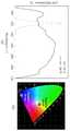
도 7은 청색 발광 조건에서 활성층이 평면 구조인 경우 및 다중면(multi-facet) 이종접합구조(Doublehetero: DH)인 경우의 광루미네선스 (photoluminescence) 차이를 도시한 것이다.7 shows the photoluminescence difference in the case where the active layer has a planar structure and the multi-facet heterojunction structure (DH) under the blue light emission condition.
광루미네선스는 물질이 빛에 의해 자극 받아 스스로 빛을 내는 현상을 의미한다.Luminousness means the phenomenon that a substance is stimulated by light and emits light by itself.
Sample A는 활성층이 평면 구조인 발광다이오드이고, Sample B는 본 발명에 따른 활성층이 다중면 구조인 발광다이오드이다.Sample A is a light emitting diode in which the active layer is a planar structure, and Sample B is a light emitting diode in which the active layer according to the present invention is a multi-plane structure.
도 7에서 볼 수 있는 바와 같이, Sample A의 경우에는 약 440 ~ 450 nm 영역의 파장만이 강하게 방출되고, Sample B의 경우에는 약 450 ~ 650 nm 영역의 파장이 방출되는 것을 알 수 있다. 즉, Sample A는 청색광을, Sample B는 백색광을 방출한다. 또한, Sample A 그래프의 아랫부분 면적 보다 Sample B 그래프의 아랫부분 면적이 더 넓은 것으로써, Sample B의 발광층의 파장이 다양하다는 것을 확인할 수 있다.As can be seen from FIG. 7, it can be seen that only a wavelength of about 440-450 nm is strongly emitted in the case of Sample A, and a wavelength of about 450-650 nm is emitted in the case of Sample B. That is, Sample A emits blue light and Sample B emits white light. Also, it can be seen that the wavelength of the light emitting layer of Sample B is varied by making the bottom area of the Sample B graph wider than the bottom area of the Sample A graph.
도 8은 청색 발광 조건에서 활성층이 평면 구조인 발광다이오드의 경우 및 다중면(multi-facet) 구조인 발광다이오드의 경우의 전기루미네선스 (electroluminescence) 차이를 도시한 것이다.FIG. 8 shows the electroluminescence difference in the case of the light emitting diode having the planar structure of the active layer and the light emitting diode having the multi-facet structure under the blue light emission condition.
전기루미네선스는 물질에 강한 전기장을 걸면 빛을 내는 현상을 의미하며, 전기에너지가 빛 에너지로 전환되는 것이다.Electroluminescence means the phenomenon of emitting light when a strong electric field is applied to the material, and electric energy is converted to light energy.
Sample A는 활성층이 평면 구조인 발광다이오드이고, Sample B는 본 발명에 따른 활성층이 다중면 구조인 발광다이오드이다.Sample A is a light emitting diode in which the active layer is a planar structure, and Sample B is a light emitting diode in which the active layer according to the present invention is a multi-plane structure.
도 8(a)에서 볼 수 있는 바와 같이 상기 Sample A 및 Sample B에 각각 20mA의 전류를 흘려 주었을 때, 상기 도 7에서와 마찬가지로, Sample A의 경우에는 약 450 nm 영역의 파장만이 강하게 방출되고, Sample B의 경우에는 약 400 ~ 700 nm 영역의 파장이 방출되는 것을 알 수 있다.As shown in FIG. 8 (a), when a current of 20 mA is applied to each of Sample A and Sample B, only the wavelength of about 450 nm is strongly emitted in the case of Sample A , And in the case of Sample B, a wavelength of about 400 to 700 nm is emitted.
도 8(b)에서 볼 수 있는 바와 같이 Sample A는 청색광을, Sample B는 백색광을 방출하는 것을 확인할 수 있다.As can be seen from FIG. 8 (b), Sample A emits blue light and Sample B emits white light.
이상의 설명은 본 발명의 기술 사상을 예시적으로 설명한 것에 불과한 것으로서, 본 발명이 속하는 기술 분야에서 통상의 지식을 가진 자라면 본 발명의 본질적인 특성에서 벗어나지 않는 범위에서 다양한 수정 및 변형이 가능할 것이다. 따라서 본 발명에 기재된 실시예들은 본 발명의 기술 사상을 한정하기 위한 것이 아니라 설명하기 위한 것이고, 이러한 실시예에 한정되는 것은 아니다. 본 발명의 보호 범위는 아래의 청구범위에 의해서 해석되어야 하며, 그와 동등한 범위 내에 있는 모든 기술 사상은 본 발명의 권리범위에 포함되는 것으로 해석되어야 할 것이다.The foregoing description is merely illustrative of the technical idea of the present invention, and various changes and modifications may be made by those skilled in the art without departing from the essential characteristics of the present invention. Therefore, the embodiments described in the present invention are not intended to limit the technical spirit of the present invention but to illustrate the present invention. The scope of protection of the present invention should be construed according to the following claims, and all technical ideas within the scope of equivalents thereof should be construed as being included in the scope of the present invention.
310: 기판
320: N-GaN층
330: 다공성 SiNx 나노 마스크층
340: 다중면(multi-facet) 구조의 GaN층
350: 다중면(multi-facet)구조의 활성층
360: P-GaN층310: substrate
320: N-GaN layer
330: Porous SiNx nanomask layer
340: a multi-facet GaN layer
350: active layer of multi-facet structure
360: P-GaN layer
Claims (10)
Translated fromKorean상기 다공성 나노 마스크층의 상부에 제1 질화물 반도체가 다중면(multi-facet) 구조로 형성되는 제1 질화물 반도체층; 및
상기 제1 질화물 반도체층의 상부에 제2 질화물 반도체가 다중면(multi-facet) 구조로 형성되는 활성층을 포함하며,
상기 제1 질화물 반도체층은, 하층부 및 상층부로 구성되고,
상기 하층부는 상기 다공성 나노 마스크층의 구멍을 통해 성장된 복수의 기둥 형상으로 서로 이격되어 형성되고, 상기 상층부는 상기 복수의 기둥 형상 중 적어도 일부의 측면이 서로 결합되어 형성되는 것을 특징으로 하는 백색 발광다이오드.
Porous nano-mask layer;
A first nitride semiconductor layer in which a first nitride semiconductor is formed in a multi-facet structure on the porous nanomask layer; And
And an active layer formed on the first nitride semiconductor layer, the second nitride semiconductor being formed in a multi-facet structure,
The first nitride semiconductor layer is composed of a lower layer portion and an upper layer portion,
Wherein the lower layer portion is formed in a plurality of columns spaced apart from each other through a hole of the porous nanomask layer, and the upper layer portion is formed by joining at least a part of the side surfaces of the plurality of columnar portions to each other. diode.
상기 다공성 나노 마스크층의 구멍의 크기는 수nm 내지 수백nm인 것을 특징으로 하는 백색 발광다이오드.
The method according to claim 1,
Wherein a size of the hole of the porous nanomask layer is several nm to several hundreds of nm.
상기 활성층은,
상기 제2 질화물 반도체 및 제3 질화물 반도체가 다중면(multi-facet) 구조로 형성되는 것을 특징으로 하는 백색 발광다이오드.
The method according to claim 1,
Wherein,
Wherein the second nitride semiconductor and the third nitride semiconductor are formed in a multi-facet structure.
상기 제2 질화물 반도체는,
InGaN이고, 상기 InGaN는 상기 제1 질화물 반도체층의 상부에 불균일한 두께로 형성되는 것을 특징으로 하는 백색 발광다이오드.
The method according to claim 1,
The second nitride semiconductor layer
InGaN is formed on the first nitride semiconductor layer, and the InGaN is formed on the first nitride semiconductor layer to have an uneven thickness.
상기 제2 질화물 반도체는,
InGaN이고, 상기 InGaN는 상기 제1 질화물 반도체층의 상부에 불균일한 인듐(In) 농도로 형성되는 것을 특징으로 하는 백색 발광다이오드.
The method according to claim 1,
The second nitride semiconductor layer
Wherein the first nitride semiconductor layer is formed of InGaN and the InGaN is formed of an indium (In) concentration non-uniform on the first nitride semiconductor layer.
상기 다공성 나노 마스크층의 상부에 제1 질화물 반도체를 성장시켜 다중면(multi-facet) 구조의 제1 질화물 반도체층을 형성시키는 단계; 및
상기 제1 질화물 반도체층의 상부에 제2 질화물 반도체를 성장시켜 다중면(multi-facet) 구조의 활성층을 형성시키는 단계를 포함하며,
상기 제1 질화물 반도체층을 형성시키는 단계는, 상기 다공성 나노 마스크층의 구멍을 통해 서로 이격된 복수의 기둥 형상을 형성시키다가, 소정의 높이 이상에서는 상기 복수의 기둥 형상 중 적어도 일부의 측면이 서로 결합되도록 형성시키고,
상기 각 단계는, MOCVD(Metal Organic Chemical Vapor Deposition)를 이용하여 인시추(in-situ) 방식으로 수행되는 것을 특징으로 하는 백색 발광다이오드 제조 방법.
Forming a porous nanomask layer;
Growing a first nitride semiconductor on the porous nanomask layer to form a first nitride semiconductor layer having a multi-facet structure; And
And growing a second nitride semiconductor on the first nitride semiconductor layer to form an active layer having a multi-facet structure,
The step of forming the first nitride semiconductor layer may include forming a plurality of pillars spaced apart from each other through the holes of the porous nanomask layer and arranging at least a part of the side surfaces of the plurality of pillars at a predetermined height or higher, And then,
Wherein each of the above steps is performed in-situ using MOCVD (Metal Organic Chemical Vapor Deposition).
상기 활성층을 형성시키는 단계는,
상기 제2 질화물 반도체 및 제3 질화물 반도체를 다중면(multi-facet) 구조로 형성시키는 것을 특징으로 하는 백색 발광다이오드 제조 방법.
The method according to claim 6,
The forming of the active layer may include:
Wherein the second nitride semiconductor and the third nitride semiconductor are formed in a multi-facet structure.
상기 제2 질화물 반도체는,
InGaN이고, 상기 InGaN는 상기 제1 질화물 반도체층의 상부에 불균일한 두께로 형성되는 것을 특징으로 하는 백색 발광다이오드 제조 방법.
The method according to claim 6,
The second nitride semiconductor layer
Wherein the first nitride semiconductor layer is made of InGaN and the InGaN is formed on the first nitride semiconductor layer to have an uneven thickness.
상기 제2 질화물 반도체는,
InGaN이고, 상기 InGaN는 상기 제1 질화물 반도체층의 상부에 불균일한 인듐(In) 농도로 형성되는 것을 특징으로 하는 백색 발광다이오드 제조 방법.
The method according to claim 6,
The second nitride semiconductor layer
Wherein the first nitride semiconductor layer is formed of InGaN and the InGaN is formed of an indium (In) concentration non-uniform on the first nitride semiconductor layer.
Priority Applications (1)
| Application Number | Priority Date | Filing Date | Title |
|---|---|---|---|
| KR1020150117534AKR101666836B1 (en) | 2015-08-20 | 2015-08-20 | Growth technique for phosphor-free white light emitting diode |
Applications Claiming Priority (1)
| Application Number | Priority Date | Filing Date | Title |
|---|---|---|---|
| KR1020150117534AKR101666836B1 (en) | 2015-08-20 | 2015-08-20 | Growth technique for phosphor-free white light emitting diode |
Publications (1)
| Publication Number | Publication Date |
|---|---|
| KR101666836B1true KR101666836B1 (en) | 2016-10-17 |
Family
ID=57250192
Family Applications (1)
| Application Number | Title | Priority Date | Filing Date |
|---|---|---|---|
| KR1020150117534AActiveKR101666836B1 (en) | 2015-08-20 | 2015-08-20 | Growth technique for phosphor-free white light emitting diode |
Country Status (1)
| Country | Link |
|---|---|
| KR (1) | KR101666836B1 (en) |
Cited By (5)
| Publication number | Priority date | Publication date | Assignee | Title |
|---|---|---|---|---|
| CN110429159A (en)* | 2019-06-24 | 2019-11-08 | 厦门大学 | The unstressed configuration powder Single chip white light LED component and manufacturing method of adjustable color |
| US11362136B2 (en) | 2019-08-19 | 2022-06-14 | Samsung Electronics Co., Ltd. | Display apparatus |
| WO2023128561A1 (en)* | 2021-12-30 | 2023-07-06 | 서울바이오시스주식회사 | Light-emitting element and light-emitting module comprising same |
| US11699775B2 (en) | 2020-01-22 | 2023-07-11 | Samsung Electronics Co.. Ltd. | Semiconductor LED and method of manufacturing the same |
| US12107186B2 (en) | 2020-01-22 | 2024-10-01 | Samsung Electronics Co., Ltd. | Semiconductor LED and method of manufacturing the same |
Citations (2)
| Publication number | Priority date | Publication date | Assignee | Title |
|---|---|---|---|---|
| KR100646570B1 (en)* | 2005-12-26 | 2006-11-15 | 엘지전자 주식회사 | Light emitting diodes and manufacturing method |
| KR20110131801A (en)* | 2010-05-31 | 2011-12-07 | 삼성전자주식회사 | How to make light emitting devices and multi-wavelength light |
- 2015
- 2015-08-20KRKR1020150117534Apatent/KR101666836B1/enactiveActive
Patent Citations (2)
| Publication number | Priority date | Publication date | Assignee | Title |
|---|---|---|---|---|
| KR100646570B1 (en)* | 2005-12-26 | 2006-11-15 | 엘지전자 주식회사 | Light emitting diodes and manufacturing method |
| KR20110131801A (en)* | 2010-05-31 | 2011-12-07 | 삼성전자주식회사 | How to make light emitting devices and multi-wavelength light |
Non-Patent Citations (1)
| Title |
|---|
| InGaN/GaN multiple quantum wells grown on microfacets for white-light generation, APPLIED PHYSICS LETTERS 93, (2008. 12. 17. 공개) |
Cited By (7)
| Publication number | Priority date | Publication date | Assignee | Title |
|---|---|---|---|---|
| CN110429159A (en)* | 2019-06-24 | 2019-11-08 | 厦门大学 | The unstressed configuration powder Single chip white light LED component and manufacturing method of adjustable color |
| US11362136B2 (en) | 2019-08-19 | 2022-06-14 | Samsung Electronics Co., Ltd. | Display apparatus |
| US11764254B2 (en) | 2019-08-19 | 2023-09-19 | Samsung Electronics Co., Ltd. | Display apparatus |
| US11923400B2 (en) | 2019-08-19 | 2024-03-05 | Samsung Electronics Co., Ltd. | Display apparatus |
| US11699775B2 (en) | 2020-01-22 | 2023-07-11 | Samsung Electronics Co.. Ltd. | Semiconductor LED and method of manufacturing the same |
| US12107186B2 (en) | 2020-01-22 | 2024-10-01 | Samsung Electronics Co., Ltd. | Semiconductor LED and method of manufacturing the same |
| WO2023128561A1 (en)* | 2021-12-30 | 2023-07-06 | 서울바이오시스주식회사 | Light-emitting element and light-emitting module comprising same |
Similar Documents
| Publication | Publication Date | Title |
|---|---|---|
| US7998771B2 (en) | Manufacturing method of light emitting diode including current spreading layer | |
| US8399876B2 (en) | Semiconductor dies, light-emitting devices, methods of manufacturing and methods of generating multi-wavelength light | |
| US9911898B2 (en) | Ultraviolet light-emitting device | |
| CN100403564C (en) | Monolithic multi-color, multi-quantum well semiconductor light-emitting diode and method of manufacturing same | |
| US9978905B2 (en) | Semiconductor structures having active regions comprising InGaN and methods of forming such semiconductor structures | |
| US9397258B2 (en) | Semiconductor structures having active regions comprising InGaN, methods of forming such semiconductor structures, and light emitting devices formed from such semiconductor structures | |
| CN107004743B (en) | Semiconductor light-emitting element | |
| US9246057B2 (en) | Semiconductor structures having active regions comprising InGaN, methods of forming such semiconductor structures, and light emitting devices formed from such semiconductor structures | |
| KR102790443B1 (en) | LED Array | |
| KR101666836B1 (en) | Growth technique for phosphor-free white light emitting diode | |
| TW201937753A (en) | Nitride semiconductor light-emitting element | |
| CN104916748A (en) | Optical semiconductor element | |
| US9543476B2 (en) | UV light emitting diode and method of fabricating the same | |
| US8222655B2 (en) | Semiconductor light-emitting device and process for producing the same | |
| US20090315063A1 (en) | Light emitting device and method of manufacturing the same | |
| KR101373804B1 (en) | White light emitting diode and fabrication method thereof | |
| KR100853935B1 (en) | Semiconductor light emitting diode and method of manufacturing the same | |
| KR102817111B1 (en) | Semiconductor lighting source for display and method of manufacturing the same | |
| KR20130110748A (en) | Light emitting device and method of manufacturing the same | |
| US20250143017A1 (en) | Tunnel-junction cascade led with different pump wavelengths | |
| KR100608919B1 (en) | Light emitting device and manufacturing method thereof | |
| US10186634B2 (en) | Semiconductor light-emitting element | |
| KR20130029933A (en) | Light emitting device and method of manufacturing the same | |
| KR20130007029A (en) | Nitride based light emitting device having improved light extraction efficiedncy and method for fabricating the same | |
| KR20110118935A (en) | Light emitting diode having multiple wavelengths and manufacturing method |
Legal Events
| Date | Code | Title | Description |
|---|---|---|---|
| PA0109 | Patent application | Patent event code:PA01091R01D Comment text:Patent Application Patent event date:20150820 | |
| PA0201 | Request for examination | ||
| PE0902 | Notice of grounds for rejection | Comment text:Notification of reason for refusal Patent event date:20160112 Patent event code:PE09021S01D | |
| PE0701 | Decision of registration | Patent event code:PE07011S01D Comment text:Decision to Grant Registration Patent event date:20160727 | |
| GRNT | Written decision to grant | ||
| PR0701 | Registration of establishment | Comment text:Registration of Establishment Patent event date:20161011 Patent event code:PR07011E01D | |
| PR1002 | Payment of registration fee | Payment date:20161012 End annual number:3 Start annual number:1 | |
| PG1601 | Publication of registration | ||
| FPAY | Annual fee payment | Payment date:20191007 Year of fee payment:4 | |
| PR1001 | Payment of annual fee | Payment date:20191007 Start annual number:4 End annual number:4 | |
| PR1001 | Payment of annual fee | Payment date:20201006 Start annual number:5 End annual number:5 |