KR101666192B1 - Semiconductor chip and semiconductor module having the same - Google Patents
Semiconductor chip and semiconductor module having the sameDownload PDFInfo
- Publication number
- KR101666192B1 KR101666192B1KR1020100009641AKR20100009641AKR101666192B1KR 101666192 B1KR101666192 B1KR 101666192B1KR 1020100009641 AKR1020100009641 AKR 1020100009641AKR 20100009641 AKR20100009641 AKR 20100009641AKR 101666192 B1KR101666192 B1KR 101666192B1
- Authority
- KR
- South Korea
- Prior art keywords
- semiconductor chip
- rewiring pattern
- impedance
- edge
- pad
- Prior art date
- Legal status (The legal status is an assumption and is not a legal conclusion. Google has not performed a legal analysis and makes no representation as to the accuracy of the status listed.)
- Active
Links
Images


Classifications
- G—PHYSICS
- G11—INFORMATION STORAGE
- G11C—STATIC STORES
- G11C5/00—Details of stores covered by group G11C11/00
- G11C5/02—Disposition of storage elements, e.g. in the form of a matrix array
- G—PHYSICS
- G11—INFORMATION STORAGE
- G11C—STATIC STORES
- G11C5/00—Details of stores covered by group G11C11/00
- G11C5/02—Disposition of storage elements, e.g. in the form of a matrix array
- G11C5/025—Geometric lay-out considerations of storage- and peripheral-blocks in a semiconductor storage device
- G—PHYSICS
- G11—INFORMATION STORAGE
- G11C—STATIC STORES
- G11C5/00—Details of stores covered by group G11C11/00
- G11C5/02—Disposition of storage elements, e.g. in the form of a matrix array
- G11C5/04—Supports for storage elements, e.g. memory modules; Mounting or fixing of storage elements on such supports
- G—PHYSICS
- G11—INFORMATION STORAGE
- G11C—STATIC STORES
- G11C5/00—Details of stores covered by group G11C11/00
- G11C5/06—Arrangements for interconnecting storage elements electrically, e.g. by wiring
- G—PHYSICS
- G11—INFORMATION STORAGE
- G11C—STATIC STORES
- G11C5/00—Details of stores covered by group G11C11/00
- G11C5/06—Arrangements for interconnecting storage elements electrically, e.g. by wiring
- G11C5/063—Voltage and signal distribution in integrated semi-conductor memory access lines, e.g. word-line, bit-line, cross-over resistance, propagation delay
- G—PHYSICS
- G11—INFORMATION STORAGE
- G11C—STATIC STORES
- G11C7/00—Arrangements for writing information into, or reading information out from, a digital store
- G11C7/10—Input/output [I/O] data interface arrangements, e.g. I/O data control circuits, I/O data buffers
- H—ELECTRICITY
- H01—ELECTRIC ELEMENTS
- H01L—SEMICONDUCTOR DEVICES NOT COVERED BY CLASS H10
- H01L25/00—Assemblies consisting of a plurality of semiconductor or other solid state devices
- H01L25/03—Assemblies consisting of a plurality of semiconductor or other solid state devices all the devices being of a type provided for in a single subclass of subclasses H10B, H10D, H10F, H10H, H10K or H10N, e.g. assemblies of rectifier diodes
- H01L25/04—Assemblies consisting of a plurality of semiconductor or other solid state devices all the devices being of a type provided for in a single subclass of subclasses H10B, H10D, H10F, H10H, H10K or H10N, e.g. assemblies of rectifier diodes the devices not having separate containers
- H01L25/065—Assemblies consisting of a plurality of semiconductor or other solid state devices all the devices being of a type provided for in a single subclass of subclasses H10B, H10D, H10F, H10H, H10K or H10N, e.g. assemblies of rectifier diodes the devices not having separate containers the devices being of a type provided for in group H10D89/00
- H01L25/0657—Stacked arrangements of devices
- H—ELECTRICITY
- H03—ELECTRONIC CIRCUITRY
- H03K—PULSE TECHNIQUE
- H03K19/00—Logic circuits, i.e. having at least two inputs acting on one output; Inverting circuits
- H03K19/003—Modifications for increasing the reliability for protection
- H—ELECTRICITY
- H01—ELECTRIC ELEMENTS
- H01L—SEMICONDUCTOR DEVICES NOT COVERED BY CLASS H10
- H01L2924/00—Indexing scheme for arrangements or methods for connecting or disconnecting semiconductor or solid-state bodies as covered by H01L24/00
- H—ELECTRICITY
- H01—ELECTRIC ELEMENTS
- H01L—SEMICONDUCTOR DEVICES NOT COVERED BY CLASS H10
- H01L2924/00—Indexing scheme for arrangements or methods for connecting or disconnecting semiconductor or solid-state bodies as covered by H01L24/00
- H01L2924/0001—Technical content checked by a classifier
- H01L2924/0002—Not covered by any one of groups H01L24/00, H01L24/00 and H01L2224/00
Landscapes
- Engineering & Computer Science (AREA)
- Physics & Mathematics (AREA)
- Computer Hardware Design (AREA)
- Microelectronics & Electronic Packaging (AREA)
- General Engineering & Computer Science (AREA)
- Mathematical Physics (AREA)
- Computing Systems (AREA)
- Power Engineering (AREA)
- Condensed Matter Physics & Semiconductors (AREA)
- General Physics & Mathematics (AREA)
- Semiconductor Integrated Circuits (AREA)
- Internal Circuitry In Semiconductor Integrated Circuit Devices (AREA)
- Semiconductor Memories (AREA)
Abstract
Translated fromKorean
Description
Translated fromKorean본 발명은 반도체 칩 및 이를 포함하는 반도체 모듈에 관한 것으로, 더욱 구체적으로는 터미네이션 저항을 포함하는 반도체 칩 및 반도체 모듈에 관한 것이다.The present invention relates to a semiconductor chip and a semiconductor module including the semiconductor chip, and more particularly to a semiconductor chip and a semiconductor module including a termination resistor.
터미네이션(termination) 저항은 전송 선로의 단부에 부착하는 저항으로서, 신호를 흡수함으로써 상기 신호들이 반사되는 것을 방지하는 역할을 수행한다. 디램(DRAM, dynamic random access memory)과 같은 메모리 반도체 소자의 동작 속도가 점점 증가함에 따라, 데이터 신호 및 제어 신호의 반사를 방지하고 안정적으로 신호를 전송하기 위해 터미네이션 저항이 구현된다.A termination resistance is a resistance attached to an end of a transmission line, and serves to prevent the signals from being reflected by absorbing the signal. As the operating speed of memory semiconductor devices such as dynamic random access memory (DRAM) increases, termination resistors are implemented to prevent reflection of data signals and control signals and to transmit signals stably.
본 발명이 해결하고자 하는 과제는, 전기적 특성이 개선된 반도체 칩 및 반도체 모듈을 제공하는 것이다.SUMMARY OF THE INVENTION It is an object of the present invention to provide a semiconductor chip and a semiconductor module with improved electrical characteristics.
본 발명의 일 태양에 의한 반도체 칩이 제공된다. 상기 반도체 칩은 복수개의 메모리 셀들, 상기 반도체 칩 상의 센터 영역에 배치되며, 상기 메모리 셀들과 연결된 적어도 하나의 제 1 센터 패드, 상기 반도체 칩 상의 에지 영역에 배치되며, 제 1 전송 선로와 연결된 적어도 하나의 제 1 에지 패드, 상기 반도체 칩 상의 에지 영역에 배치되며, 칩셋 전압 인가부와 연결된 적어도 하나의 제 2 에지 패드, 상기 제 1 센터 패드와 상기 제 1 에지 패드 사이에 연결된 적어도 하나의 제 1 재배선 패턴, 및 상기 제 1 에지 패드와 상기 제 2 에지 패드 사이에 연결된 적어도 하나의 제 2 재배선 패턴을 포함할 수 있다.A semiconductor chip according to an aspect of the present invention is provided. The semiconductor chip includes a plurality of memory cells, at least one first center pad disposed in a center region on the semiconductor chip and connected to the memory cells, at least one first center pad disposed in an edge region on the semiconductor chip, At least one second edge pad disposed at an edge region on the semiconductor chip and connected to the chipset voltage application portion, at least one first growth pad connected between the first center pad and the first edge pad A line pattern, and at least one second rewiring pattern connected between the first edge pad and the second edge pad.
상기 반도체 칩의 일 예에 의하면, 상기 제 2 재배선 패턴의 임피던스는 상기 제 1 전송 선로의 임피던스와 임피던스 매칭될 수 있다.According to an example of the semiconductor chip, the impedance of the second rewiring pattern may be impedance-matched with the impedance of the first transmission line.
상기 반도체 칩의 다른 예에 의하면, 상기 제 1 재배선 패턴은 제 1 방향을 따라 확장되고, 상기 제 2 재배선 패턴은 상기 제 1 방향과 수직한 제 2 방향을 따라 확장될 수 있다.According to another example of the semiconductor chip, the first rewiring pattern may extend along a first direction, and the second rewiring pattern may extend along a second direction perpendicular to the first direction.
상기 반도체 칩의 다른 예에 의하면, 상기 제 2 재배선 패턴의 임피던스는 상기 제 1 재배선 패턴의 임피던스보다 클 수 있다.According to another example of the semiconductor chip, the impedance of the second rewiring pattern may be larger than the impedance of the first rewiring pattern.
상기 반도체 칩의 다른 예에 의하면, 상기 반도체 칩은 상기 반도체 칩 상의 센터 영역에 배치되며, 상기 메모리 셀들과 연결된 적어도 하나의 제 2 센터 패드, 상기 반도체 칩 상의 에지 영역에 배치되며, 제 2 전송 선로와 연결된 적어도 하나의 제 3 에지 패드, 및 상기 제 2 센터 패드와 상기 제 3 에지 패드 사이에 연결된 적어도 하나의 제 3 재배선 패턴을 더 포함할 수 있다.According to another example of the semiconductor chip, the semiconductor chip is disposed in a center region on the semiconductor chip, and includes at least one second center pad connected to the memory cells, an edge region disposed on the semiconductor chip, And at least one third rewiring pattern connected between the second center pad and the third edge pad.
상기 반도체 칩의 다른 예에 의하면, 상기 제 3 재배선 패턴의 임피던스는, 상기 제 2 전송 선로의 임피던스 및 상기 제 2 센터 패드로부터 상기 메모리 셀들까지의 임피던스의 차이와 임피던스 매칭될 수 있다.According to another example of the semiconductor chip, the impedance of the third rewiring pattern may be impedance-matched with the impedance of the second transmission line and the impedance of the memory cells from the second center pad.
상기 반도체 칩의 다른 예에 의하면, 상기 제 1 전송 선로는 커맨드(command), 어드레스(address), 및 클럭(clock) 신호를 전송하고, 상기 제 2 전송 선로는 데이터 신호를 전송할 수 있다.According to another example of the semiconductor chip, the first transmission line may transmit a command, an address, and a clock signal, and the second transmission line may transmit a data signal.
상기 반도체 칩의 다른 예에 의하면, 상기 제 1 재배선 패턴 내지 상기 제 3 재배선 패턴은 상기 에지 영역과 상기 센터 영역 사이의 영역에 형성될 수 있다.According to another example of the semiconductor chip, the first rewiring pattern to the third rewiring pattern may be formed in an area between the edge area and the center area.
상기 반도체 칩의 다른 예에 의하면, 상기 제 1 재배선 패턴 내지 상기 제 3 재배선 패턴 중 적어도 하나는 미앤더(meander) 부재를 포함할 수 있다.According to another example of the semiconductor chip, at least one of the first rewiring pattern to the third rewiring pattern may include a meander member.
상기 반도체 칩의 다른 예에 의하면, 상기 제 2 재배선 패턴 및 상기 제 3 재배선 패턴 중 적어도 하나는 병렬로 연결된 복수개의 재배선 패턴들을 포함하고, 상기 반도체 칩은 상기 재배선 패턴들 각각과 연결된 금속 퓨즈(fuse)를 더 포함할 수 있다.According to another example of the semiconductor chip, at least one of the second rewiring pattern and the third rewiring pattern includes a plurality of rewiring patterns connected in parallel, and the semiconductor chip is connected to each of the rewiring patterns And may further include a metal fuse.
상기 반도체 칩의 다른 예에 의하면, 상기 금속 퓨즈는 라인 형태이고, 상기 금속 퓨즈는 상기 라인의 양단 사이에 퓨즈 블로잉부를 포함하며, 상기 라인의 양단은 불순물 이온을 포함할 수 있다.According to another example of the semiconductor chip, the metal fuse is in the form of a line, and the metal fuse includes a fuse blowing portion between both ends of the line, and both ends of the line may include impurity ions.
상기 반도체 칩의 다른 예에 의하면, 상기 제 2 재배선 패턴의 임피던스는 상기 제 3 재배선 패턴의 임피던스보다 클 수 있다.According to another example of the semiconductor chip, the impedance of the second rewiring pattern may be greater than the impedance of the third rewiring pattern.
상기 반도체 칩의 다른 예에 의하면, 상기 제 2 재배선 패턴의 길이는 상기 제 3 재배선 패턴의 길이보다 클 수 있다.According to another example of the semiconductor chip, the length of the second rewiring pattern may be greater than the length of the third rewiring pattern.
상기 반도체 칩의 다른 예에 의하면, 상기 제 2 재배선 패턴의 저항률은 상기 제 3 재배선 패턴의 저항률보다 클 수 있다.According to another example of the semiconductor chip, the resistivity of the second rewiring pattern may be greater than that of the third rewiring pattern.
본 발명의 일 태양에 의한 반도체 모듈이 제공된다. 상기 반도체 모듈은 복수개의 메모리 셀들을 포함하는 복수개의 반도체 칩들, 상기 반도체 칩들을 탑재하는 기판, 상기 기판 상에 탑재된 칩셋 전압 인가부, 및 상기 기판 상에 형성되며, 상기 반도체 칩들 각각에 커맨드, 어드레스, 및 클럭 신호를 전송하는 복수개의 제 1 전송 선로를 포함하고, 상기 반도체 칩들 중 적어도 하나의 반도체 칩은 상기 반도체 칩 상의 센터 영역에 배치되며, 상기 메모리 셀들과 연결된 적어도 하나의 제 1 센터 패드, 상기 반도체 칩 상의 에지 영역에 배치되며, 상기 제 1 전송 선로와 연결된 적어도 하나의 제 1 에지 패드, 상기 반도체 칩 상의 에지 영역에 배치되며, 상기 칩셋 전압 인가부와 연결된 적어도 하나의 제 2 에지 패드, 상기 제 1 센터 패드와 상기 제 1 에지 패드 사이에 연결된 적어도 하나의 제 1 재배선 패턴, 및 상기 제 1 에지 패드와 상기 제 2 에지 패드 사이에 연결된 적어도 하나의 제 2 재배선 패턴을 포함할 수 있다.A semiconductor module according to an aspect of the present invention is provided. The semiconductor module may include a plurality of semiconductor chips including a plurality of memory cells, a substrate on which the semiconductor chips are mounted, a chipset voltage applying unit mounted on the substrate, and a semiconductor chip formed on the substrate, Address, and clock signal, wherein at least one semiconductor chip of the semiconductor chips is disposed in a center region on the semiconductor chip, and at least one first center pad connected to the memory cells, At least one first edge pad disposed in an edge region on the semiconductor chip and connected to the first transmission line, at least one second edge pad disposed in an edge region on the semiconductor chip, At least one first rewiring pattern connected between the first center pad and the first edge pad, And at least one second rewiring pattern connected between the first edge pad and the second edge pad.
상기 반도체 모듈의 일 예에 의하면, 상기 제 1 전송 선로들은, 상기 기판의 외부 단자와 상기 반도체 칩들 중 하나의 반도체 칩의 제 1 에지 패드 사이를 연결하는 제 1 배선 라인, 및 상기 반도체 칩들의 상기 제 1 에지 패드들 사이를 연결하는 복수개의 제 2 배선 라인들을 포함하고, 상기 제 1 배선 라인과 상기 제 2 배선 라인들 각각의 임피던스는 실질적으로 동일하며, 상기 제 2 재배선 패턴의 임피던스는 상기 제 1 배선 라인의 임피던스와 임피던스 매칭될 수 있다.According to an example of the semiconductor module, the first transmission lines include a first wiring line connecting between an external terminal of the substrate and a first edge pad of one semiconductor chip of the semiconductor chips, Wherein the impedance of each of the first wiring line and the second wiring line is substantially the same and the impedance of the second wiring line pattern is substantially the same as the impedance of the second wiring line. The impedance and the impedance of the first wiring line can be matched.
상기 반도체 모듈의 다른 예에 의하면, 상기 반도체 모듈은 상기 기판 상에 형성되며, 상기 반도체 칩들 각각에 데이터 신호를 전송하는 복수개의 제 2 전송 선로를 더 포함하고, 상기 반도체 칩들 중 적어도 하나는, 상기 반도체 칩 상의 센터 영역에 배치되며, 상기 메모리 셀들과 연결된 적어도 하나의 제 2 센터 패드, 상기 반도체 칩 상의 에지 영역에 배치되며, 상기 제 2 전송 선로와 연결된 적어도 하나의 제 3 에지 패드, 및 상기 제 2 센터 패드와 상기 제 3 에지 패드 사이에 연결된 적어도 하나의 제 3 재배선 패턴을 더 포함할 수 있다.According to another example of the semiconductor module, the semiconductor module further includes a plurality of second transmission lines formed on the substrate and transmitting a data signal to each of the semiconductor chips, wherein at least one of the semiconductor chips At least one second center pad disposed in a center region on the semiconductor chip and connected to the memory cells, at least one third edge pad disposed in an edge region on the semiconductor chip and connected to the second transmission line, And at least one third rewiring pattern connected between the second center pad and the third edge pad.
상기 반도체 모듈의 다른 예에 의하면, 상기 제 2 전송 선로들은 반도체 칩들의 제 3 에지 패드와 상기 기판의 상기 외부 단자 사이를 연결하는 제 3 배선 라인을 포함하며, 상기 제 3 재배선 패턴의 임피던스는, 상기 제 3 배선 라인의 임피던스 및 상기 제 2 센터 패드로부터 상기 메모리 셀들까지의 임피던스의 차이와 임피던스 매칭될 수 있다.According to another example of the semiconductor module, the second transmission lines include a third wiring line connecting the third edge pad of the semiconductor chips and the external terminal of the substrate, and the impedance of the third wiring pattern is , The impedance of the third wiring line, and the impedance of the memory cells from the second center pad.
상기 반도체 모듈의 다른 예에 의하면, 상기 제 1 재배선 패턴 및 상기 제 3 재배선 패턴은 제 1 방향을 따라 확장되고, 상기 제 2 재배선 패턴은 상기 제 1 방향과 수직한 제 2 방향을 따라 확장될 수 있다.According to another example of the semiconductor module, the first rewiring pattern and the third rewiring pattern extend along a first direction, and the second rewiring pattern extends along a second direction perpendicular to the first direction Can be expanded.
본 발명의 다른 태양이 의한 반도체 칩이 제공된다. 상기 반도체 칩은 복수개의 메모리 셀들, 상기 반도체 칩 상의 센터 영역에 배치되며, 상기 메모리 셀들의 비트 라인과 연결된 적어도 하나의 센터 패드, 상기 반도체 칩 상의 에지 영역에 배치되며, 데이터 전송 선로와 연결된 적어도 하나의 에지 패드, 및 상기 센터 패드와 상기 에지 패드 사이에 연결된 적어도 하나의 재배선 패턴을 포함하고, 상기 재배선 패턴의 임피던스는, 상기 데이터 전송 선로의 임피던스 및 상기 센터 패드로부터 상기 메모리 셀들까지의 임피던스의 차이와 임피던스 매칭될 수 있다.A semiconductor chip according to another aspect of the present invention is provided. The semiconductor chip includes a plurality of memory cells, at least one center pad disposed in a center region on the semiconductor chip and connected to a bit line of the memory cells, at least one center pad disposed in an edge region on the semiconductor chip, And the impedance of the rewiring pattern is determined by an impedance of the data transmission line and an impedance of the memory cell from the center pad to the memory cell, And impedance matching can be performed.
본 발명의 실시예들에 따른 반도체 칩 및 반도체 모듈은, 신호의 특성에 따른 터미네이션 저항들이 재배선 패턴으로서 반도체 칩 상에서 구현되므로, 부품간의 물리적 거리가 최소화될 수 있다. 결국 반도체 칩 및 반도체 모듈의 전기적 특성이 개선될 수 있다.In the semiconductor chip and the semiconductor module according to the embodiments of the present invention, since the termination resistors according to signal characteristics are implemented on the semiconductor chip as the rewiring pattern, the physical distance between the components can be minimized. As a result, the electrical characteristics of the semiconductor chip and the semiconductor module can be improved.
또한, 본 발명의 실시예들에 따른 반도체 칩 및 반도체 모듈은, 터미네이션 저항과 같은 수동 소자들(passive components)이 재배선 패턴으로서 반도체 칩 상에서 구현되므로, 더욱 넓은 기판의 면적을 확보할 수 있다.Further, in the semiconductor chip and the semiconductor module according to the embodiments of the present invention, passive components such as termination resistors are implemented on the semiconductor chip as a rewiring pattern, so that a wider substrate area can be secured.
도 1 은 본 발명의 기술적 사상에 따른 일부 실시예들에 의한 반도체 칩을 개략적으로 나타낸 사시도이다.
도 2 는 본 발명의 기술적 사상에 따른 일부 실시예들에 의한 반도체 칩을 개략적으로 나타낸 단면도이다.
도 3 은 본 발명의 기술적 사상에 따른 다른 실시예들에 의한 반도체 칩을 개략적으로 나타낸 사시도이다.
도 4 는 본 발명의 기술적 사상에 따른 다른 실시예들에 의한 반도체 칩을 개략적으로 나타낸 단면도이다.
도 5는 본 발명의 기술적 사상에 따른 실시예들에 의한 반도체 모듈을 개략적으로 나타낸 단면도이다.
도 6은 본 발명의 기술적 사상에 따른 실시예에 의한 컴퓨팅 시스템을 나타내는 블록도이다.1 is a perspective view schematically showing a semiconductor chip according to some embodiments according to the technical idea of the present invention.
2 is a cross-sectional view schematically showing a semiconductor chip according to some embodiments according to the technical idea of the present invention.
3 is a perspective view schematically showing a semiconductor chip according to another embodiment of the present invention.
4 is a cross-sectional view schematically showing a semiconductor chip according to another embodiment of the present invention.
5 is a cross-sectional view schematically showing a semiconductor module according to embodiments of the present invention.
6 is a block diagram illustrating a computing system according to an embodiment of the present invention.
이하, 첨부된 도면을 참조하여 본 발명의 바람직한 실시예를 상세히 설명하기로 한다.Hereinafter, preferred embodiments of the present invention will be described in detail with reference to the accompanying drawings.
본 발명의 실시예들은 당해 기술 분야에서 통상의 지식을 가진 자에게 본 발명을 더욱 완전하게 설명하기 위하여 제공되는 것이며, 아래의 실시예들은 여러 가지 다른 형태로 변형될 수 있으며, 본 발명의 범위가 아래의 실시예들로 한정되는 것은 아니다. 오히려, 이들 실시예는 본 개시를 더욱 충실하고 완전하게 하며 당업자에게 본 발명의 사상을 완전하게 전달하기 위하여 제공되는 것이다.Embodiments of the present invention are provided to more fully describe the present invention to those skilled in the art, and the following embodiments may be modified in various other forms, The present invention is not limited to the following embodiments. Rather, these embodiments are provided so that this disclosure will be more thorough and complete, and will fully convey the concept of the invention to those skilled in the art.
본 명세서에서 사용된 용어는 특정 실시예를 설명하기 위하여 사용되며, 본 발명을 제한하기 위한 것이 아니다. 본 명세서에서 사용된 바와 같이 단수 형태는 문맥상 다른 경우를 분명히 지적하는 것이 아니라면, 복수의 형태를 포함할 수 있다. 또한, 본 명세서에서 사용되는 경우 “포함한다(comprise)” 및/또는 “포함하는(comprising)”은 언급한 형상들, 숫자, 단계, 동작, 부재, 요소 및/또는 이들 그룹의 존재를 특정하는 것이며, 하나 이상의 다른 형상, 숫자, 동작, 부재, 요소 및/또는 그룹들의 존재 또는 부가를 배제하는 것이 아니다. 본 명세서에서 사용된 바와 같이, 용어 “및/또는”은 해당 열거된 항목 중 어느 하나 및 하나 이상의 모든 조합을 포함한다.The terminology used herein is for the purpose of describing particular embodiments only and is not intended to be limiting of the invention. As used herein, the singular forms "a", "an," and "the" include plural forms unless the context clearly dictates otherwise. Also, " comprise " and / or " comprising " when used herein should be interpreted as specifying the presence of stated shapes, numbers, steps, operations, elements, elements, and / And does not preclude the presence or addition of one or more other features, integers, operations, elements, elements, and / or groups. As used herein, the term " and / or " includes any and all combinations of one or more of the listed items.
본 명세서에서 제1, 제2 등의 용어가 다양한 부재, 영역 및/또는 부위들을 설명하기 위하여 사용되지만, 이들 부재, 부품, 영역, 층들 및/또는 부위들은 이들 용어에 의해 한정되어서는 안됨은 자명하다. 이들 용어는 특정 순서나 상하, 또는 우열의 의미하지 않으며, 하나의 부재, 영역 또는 부위를 다른 부재, 영역 또는 부위와 구별하기 위하여만 사용된다. 따라서, 이하 상술할 제1 부재, 영역 또는 부위는 본 발명의 가르침으로부터 벗어나지 않고서도 제2 부재, 영역 또는 부위를 지칭할 수 있다.Although the terms first, second, etc. are used herein to describe various elements, regions and / or regions, it should be understood that these elements, components, regions, layers and / Do. These terms are not intended to be in any particular order, up or down, or top-down, and are used only to distinguish one member, region or region from another member, region or region. Thus, the first member, region or region described below may refer to a second member, region or region without departing from the teachings of the present invention.
이하, 본 발명의 실시예들은 본 발명의 이상적인 실시예들을 개략적으로 도시하는 도면들을 참조하여 설명한다. 도면들에 있어서, 예를 들면, 제조 기술 및/또는 공차에 따라, 도시된 형상의 변형들이 예상될 수 있다. 따라서, 본 발명의 실시예는 본 명세서에 도시된 영역의 특정 형상에 제한된 것으로 해석되어서는 아니 되며, 예를 들면 제조상 초래되는 형상의 변화를 포함하여야 한다.Hereinafter, embodiments of the present invention will be described with reference to the drawings schematically showing ideal embodiments of the present invention. In the figures, for example, variations in the shape shown may be expected, depending on manufacturing techniques and / or tolerances. Accordingly, embodiments of the present invention should not be construed as limited to any particular shape of the regions illustrated herein, including, for example, variations in shape resulting from manufacturing.
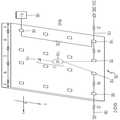
도 1 및 도 2는 본 발명의 기술적 사상에 따른 일부 실시예들에 의한 반도체 칩을 개략적으로 나타낸 사시도와 단면도이다.1 and 2 are a perspective view and a cross-sectional view schematically showing a semiconductor chip according to some embodiments according to the technical idea of the present invention.
도 1 및 도 2를 참조하면, 반도체 칩은 복수개의 메모리 셀들(110), 제 1 센터 패드(120), 제 2 센터 패드(130), 제 1 에지 패드(140), 제 2 에지 패드(150), 제 3 에지 패드(160), 제 1 재배선 패턴(R1) 및 제 2 재배선 패턴(R2)을 포함할 수 있다.1 and 2, the semiconductor chip includes a plurality of
제 1 센터 패드(120) 및 제 2 센터 패드는(130) 반도체 칩(100) 상의 센터 영역(C)에 배치되며, 메모리 셀들(110)과 전기적으로 연결될 수 있다. 더욱 구체적으로, 제 1 센터 패드(120)는 메모리 셀들(110)의 워드 라인(미도시)과 연결되고, 제 2 센터 패드(130)는 메모리 셀들(110)의 비트 라인(미도시)과 연결될 수 있다. 메모리 셀들(110)은 그라운드(115)와 연결될 수 있다.The
제 1 에지 패드(140), 제 2 에지 패드(150), 및 제 3 에지 패드(160)는 반도체 칩(100) 상의 에지 영역(E)에 배치될 수 있다. 더욱 구체적으로, 제 1 에지 패드(140)는 커맨드 신호(command signal, CMD), 어드레스 신호(address signal, ADR) 및 클럭 신호(clock, CLK)를 전송하는 제 1 전송 선로(170)와 연결될 수 있다. 제 2 에지 패드(150)는 칩셋 전압 인가부(180)와 연결될 수 있다. 제 3 에지 패드(160)는 데이터 신호(DQ)를 전송하는 제 2 전송 선로(190)와 연결될 수 있다.The
제 1 재배선 패턴(R1)은 제 1 센터 패드(120)와 제 1 에지 패드(140) 사이에 연결될 수 있다. 제 1 재배선 패턴(R1)은 제 1 방향(X)을 따라 확장되도록 형성될 수 있다.The first rewiring pattern R1 may be connected between the
제 2 재배선 패턴(R2)은 제 1 에지 패드(140)와 제 2 에지 패드(150) 사이에 연결될 수 있다. 제 2 재배선 패턴(R2)은 제 1 방향(X)과 수직한 제 2 방향(Y)을 따라 확장되도록 형성될 수 있다. 제 2 재배선 패턴(R2)의 임피던스는 제 1 재배선 패턴(R1)의 임피던스보다 클 수 있다. 제 2 재배선 패턴(R2)의 임피던스는 제 1 전송 선로(170)의 임피던스 Z1와 서로 임피던스 매칭될 수 있다. 이와 같은 임피던스 매칭을 통해, 제 2 재배선 패턴(R2)은 제 1 전송 선로(170)로부터 전송되는 커맨드, 어드레스, 및 클럭 신호들(CMD, ADR, CLK)이 반사되는 것을 방지하는 병렬 터미네이션 저항(parallel termination resistance)의 기능을 수행할 수 있다.The second rewiring pattern R2 may be connected between the
제 3 재배선 패턴(R3)은 제 2 센터 패드(130)와 제 3 에지 패드(160) 사이에 연결될 수 있다. 제 3 재배선 패턴(R3)은 제 1 방향(X)을 따라 확장되도록 형성될 수 있다. 제 3 재배선 패턴(R3)의 임피던스는 제 2 전송 선로(190)의 임피던스 Z2 및 제 2 센터 패드(130)로부터 메모리 셀들(110)까지의 임피던스 Z의 차이, 즉 Z2-Z와 서로 임피던스 매칭될 수 있다. 이와 같은 임피던스 매칭을 통해, 제 3 재배선 패턴(R3)은 제 2 전송 선로(190)로부터 전송되는 데이터 신호가 반사되는 것을 방지하는 직렬 터미네이션 저항(series termination resistance)의 기능을 수행할 수 있다.The third rewiring pattern R3 may be connected between the
제 3 재배선 패턴(R3)의 임피던스는 제 2 재배선 패턴의 임피던스(R2)보다 작을 수 있다. 제 2 재배선 패턴(R2)이 제 3 재배선 패턴(R3)의 임피던스보다 크도록, 제 2 재배선 패턴(R2)의 길이 및 저항률이 조절될 수 있다. 예를 들어, 제 2 재배선 패턴(R2)의 길이는 제 3 재배선 패턴(R3)의 길이보다 클 수 있으며, 제 2 재배선 패턴(R2)의 저항률은 제 3 재배선 패턴(R3)의 저항률보다 클 수 있다.The impedance of the third rewiring pattern R3 may be smaller than the impedance R2 of the second rewiring pattern. The length and the resistivity of the second rewiring pattern R2 can be adjusted so that the second rewiring pattern R2 is larger than the impedance of the third rewiring pattern R3. For example, the length of the second rewiring pattern R2 may be greater than the length of the third rewiring pattern R3, and the resistivity of the second rewiring pattern R2 may be greater than the length of the third rewiring pattern R3. May be greater than the resistivity.
제 1 재배선 패턴 내지 제 3 재배선 패턴들(R1, R2, R3)은 반도체 칩 상의 에지 영역(E)과 센터 영역(C) 사이의 영역(M)에 형성될 수 있다. 또한 제 1 재배선 패턴 내지 제 3 재배선 패턴들(R1, R2, R3) 중 적어도 하나는 미앤더(meander) 부재를 포함할 수 있다. 비록 도 2는 미앤더 형태의 재배선 패턴만을 개시하고 있으나, 본 발명은 이에 한정되지 않으며, 제 1 재배선 패턴 내지 제 3 재배선 패턴들(R1, R2, R3)로서 싱글 루프(single loop) 형태, 톱니 형태, 또는 나선 형태의 금속배선이 사용될 수 있다.The first to third rewiring patterns R1 to R3 may be formed in a region M between the edge region E and the center region C on the semiconductor chip. At least one of the first to third rewiring patterns R1, R2, and R3 may include a meander member. Although FIG. 2 discloses only a meander-type rewiring pattern, the present invention is not limited thereto, and a single loop may be used as the first rewiring pattern to the third rewiring patterns R1, R2, A metal wiring of a shape, a sawtooth shape, or a spiral shape can be used.
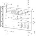
도 3 및 도 4는 본 발명의 기술적 사상에 따른 다른 실시예들에 의한 반도체 칩(100')을 개략적으로 나타낸 사시도와 단면도이다. 이 실시예에 따른 반도체 칩(100')은 도 1 및 도 2의 실시예에 따른 반도체 칩(100)의 변형된 예일 수 있다. 이하 두 실시예들에서 중복되는 설명은 생략하기로 한다.3 and 4 are a perspective view and a cross-sectional view schematically showing a semiconductor chip 100 'according to another embodiment of the present invention. The semiconductor chip 100 'according to this embodiment may be a modified example of the
도 3 및 도 4를 참조하면, 제 2 재배선 패턴(R2) 및 제 3 재배선 패턴(R3)은 병렬로 연결된 복수개의 재배선 패턴들(A, B)을 포함할 수 있다. 예를 들어, 제 2 재배선 패턴(R2)은 3개의 재배선 패턴들(A)을 포함할 수 있다. 마찬가지로, 제 3 재배선 패턴(R3)은 3개의 재배선 패턴들(B)을 포함할 수 있다. 재배선 패턴들(A. B) 각각은 미앤더 부재를 포함할 수 있다.3 and 4, the second rewiring pattern R2 and the third rewiring pattern R3 may include a plurality of rewiring patterns A and B connected in parallel. For example, the second rewiring pattern R2 may include three rewiring patterns A. Likewise, the third rewiring pattern R3 may include three rewiring patterns B. Each of the redistribution patterns A. B may include a meander member.
반도체 칩(100')은 퓨즈 블로잉부(210)를 포함하는 제 1 금속 퓨즈들(200a) 및 제 2 금속 퓨즈들(200b)을 더 포함할 수 있다. 제 1 및 제 2 금속 퓨즈들(200a, 200b)은 재배선 패턴들(A, B) 각각과 연결될 수 있다. 제 1 및 제 2 금속 퓨즈들(200a, 200b)의 퓨즈 블로잉부(210a, 210b)는 레이저 블로잉 공정에 의해 컷팅(cutting)될 수 있다. 더욱 구체적으로, 상기 레이저 블로잉 공정시 퓨즈 블로잉부(210a, 210b)에 에너지가 인가되고, 상기 에너지에 의해 발생된 열이 응축되어 퓨즈 블로잉부(210a, 210b)가 기화됨으로써 퓨즈 블로잉부가 컷팅될 수 있다. 따라서 레이저 블로잉 공정을 통해 제 1 및 제 2 금속 퓨즈들(200a, 200b)의 전기적 연결이 제거될 수 있다.The semiconductor chip 100 'may further include first metal fuses 200a and second metal fuses 200b including the fuse blowing unit 210. [ The first and second metal fuses 200a and 200b may be connected to each of the rewiring patterns A and B, respectively. The
제 1 및 제 2 금속 퓨즈(200a, 200b)는 라인 형태이고, 퓨즈 블로잉부(210a, 210b)는 라인 형태의 제 1 및 제 2 금속 퓨즈(200a, 200b)의 양단(220a, 220b) 사이에 위치할 수 있다. 산소, 질소 또는 보론(boron) 이온과 같은 불순물 이온 주입 공정을 통해, 라인 형태의 제 1 및 제 2 금속 퓨즈(200a, 200b)의 양단(220a, 220b)에 불순물 이온이 주입될 수 있다. 퓨즈 블로잉부(210a, 210b)의 양단(220a, 220b)에 불순물 이온이 주입될 경우, 양단(220a, 220b)의 전기 전도도 및 열 전도도가 감소되어 레이저 블로잉 공정시 충분한 열이 퓨즈 블로잉부(210a, 210b)에 응축될 수 있다. 즉, 퓨즈 블로잉부(210a, 210b)의 열 응출 효율이 개선되어, 효율적인 퓨즈 블로잉부(210a, 210b)의 컷팅이 가능하다.The first and second metal fuses 200a and 200b are in the form of a line and the
레이저 블로잉 공정을 통해 재배선 패턴들(A, B) 각각과 연결된 제 1 및 제 2 금속 퓨즈들(200a, 200b)을 컷팅함으로써, 제 2 및 제 3 재배선 패턴(R1, R2)의 임피던스를 변화시킬 수 있다.The first and second metal fuses 200a and 200b connected to each of the redistribution patterns A and B are cut by the laser blowing process so that the impedances of the second and third rewiring patterns R1 and R2 Can be changed.
예를 들어, 제 1 금속 퓨즈(R2)의 재배선 패턴들(A)이 모두 연결된 경우, 재배선 패턴들(A)은 3개의 미앤더 부재들이 병렬로 연결되어 있으므로, 제 2 재배선 패턴(R2)의 임피던스는 A/3이 된다. 한편, 레이저 블로잉 공정을 통해 제 1 금속 퓨즈(200a)의 재배선 패턴들(A) 중 한 개의 재배선 패턴(A)을 제거할 경우, 제 2 재배선 패턴(R2)의 임피던스는 A/2가 되며, 제 1 금속 퓨즈(R2)의 재배선 패턴들(A) 중 두 개의 재배선 패턴(A)을 제거할 경우, 제 2 재배선 패턴(R2)의 임피던스는 A가 된다.For example, when all of the rewiring patterns A of the first metal fuse R2 are connected, the rewiring patterns A are formed by connecting the second rewiring patterns R2 has an impedance of A / 3. On the other hand, when one of the redistribution patterns A of the redistribution patterns A of the
마찬가지로, 레이저 블로잉 공정을 통해 제 2 금속 퓨즈(200b)의 병렬로 연결된 재배선 패턴들(B) 중 적어도 하나의 재배선 패턴(B)이 제거될 수 있다. 따라서 제 3 재배선 패턴(R2)의 임피던스를 B, B/2, B/3과 같이 변화시킬 수 있다.Similarly, at least one of the rewiring patterns B of the rewiring patterns B connected in parallel with the
레이저 블로잉 공정을 통해 제 1 금속 퓨즈(200a)을 컷팅함으로써 제 2 재배선 패턴(R2)의 임피던스를 변화시킬 수 있고, 제 1 전송 선로(170)의 임피던스 Z1과 임피던스 매칭되는 제 2 재배선 패턴(R2)의 터미네이션 저항을 결정할 수 있다.The impedance of the second rewiring pattern R2 can be changed by cutting the
마찬가지로, 레이저 블로잉 공정을 통해 제 2 금속 퓨즈들(200b)을 컷팅함으로써 제 3 재배선 패턴(R3)의 임피던스를 변화시킬 수 있고, 제 2 전송 선로(190)의 임피던스 Z2와 제 2 센터 패드(130)로부터 메모리 셀들(110)까지의 임피던스 Z의 차이, 즉, Z2-Z와 임피던스 매칭되는 제 3 재배선 패턴(R3)의 터미네이션 저항을 결정할 수 있다.Similarly, the impedance of the third rewiring line R3 can be changed by cutting the second metal fuses 200b through the laser blowing process, and the impedance Z2 of the
비록 본 실시예의 경우 재배선 패턴들(A, B)의 임피던스가 모두 A, B로서 동일함을 전제로 발명이 설명되었으나, 본 발명은 이에 한정되지는 않으며, 서로 임피던스가 다르도록 재배선 패턴들(A, B)의 길이 또는 저항률이 조절될 수 있다.Although the present invention has been described on the assumption that the impedance of the redistribution patterns A and B is the same as A and B in the present embodiment, the present invention is not limited to this, and the redistribution patterns The lengths or the resistivity of the electrodes A and B can be adjusted.
도 5는 본 발명의 기술적 사상에 따른 실시예들에 의한 반도체 모듈(500)을 개략적으로 나타낸 단면도이다. 이 실시예에 따른 반도체 모듈(500)은 도 2의 실시예에 따른 반도체 칩(100')이 기판(50) 상에 탑재된 것이다. 이하 두 실시예들에서 중복되는 설명은 생략하기로 한다.5 is a cross-sectional view schematically showing a
도 5를 참조하면, 반도체 모듈은 기판(50), 메모리 셀들(110)을 포함하는 반도체 칩들(100'), 칩셋 전압 인가부(180), 제 1 전송 선로들(170a, 170b, 170c), 및 제 2 전송 선로들(190a, 190b, 190c)을 포함할 수 있다. 반도체 칩들(100')이 제 1 및 제 2 센터 패드들(120, 130), 제 1 내지 제 3 에지 패드들(140, 150, 160), 제 1 내지 제 3 재배선 패턴들(R1, R2, R3), 및 금속 퓨즈들(200a, 200b)을 포함할 수 있음은 상술한 바와 같다.5, the semiconductor module includes a
기판(50)은 반도체 칩(100')을 탑재할 수 있다. 기판(50)은 인쇄 회로 기판으로서 단면, 양면, 다층 인쇄 회로 기판일 수 있다. 또한 기판은 플렉시블 인쇄 회로 기판으로 구현될 수도 있다.The
칩셋 전압 인가부(180)는 기판(50) 상에 탑재되어 제 2 에지 패드(150)에 칩셋 전압(Vtt)을 인가할 수 있다. 더욱 구체적으로, 칩셋 전압 인가부(180)는 기판(50) 상에 형성된 배선 라인(미도시)으로서, 메모리 모듈(500)의 외부 단자(60)와 연결된 메인 보드(미도시)로부터 인가되는 칩셋 전압(Vtt)을 제 2 에지 패드(150)에 전달할 수 있다.The chipset
제 1 전송 선로들(170a, 170b, 170c)은 기판 상에 탑재되어 제 1 에지 패드들(140)에 커맨드, 어드레스, 및 클럭 신호들(CLK, CMD, ADR)을 전송할 수 있다. 더욱 구체적으로, 제 1 전송 선로들(170a, 170b, 170c)은 기판 상에 형성된 배선 라인으로서, 기판(50)의 외부 단자(60)와 제 1 에지 패드들(140) 사이를 연결하는 제 1 배선 라인(170a), 및 각각의 반도체 칩들(100')의 제 1 에지 패드(140)들 사이를 연결하는 제 2 배선 라인들(170b, 170c)을 포함할 수 있다. 제 1 배선 라인(170a)와 제 2 배선 라인들(170b, 170c)의 임피던스는 실질적으로 동일할 수 있다.The
제 2 전송 선로들(190a, 190b, 190c)은 기판(50) 상에 탑재되어 제 3 에지 패드들(160)에 데이터 신호(DQ)를 전송할 수 있다. 더욱 구체적으로, 제 2 전송 선로들(190a, 190b, 190c)은 기판(50) 상에 형성된 배선 라인으로서, 각각의 반도체 칩들(100')의 제 3 에지 패드들(160)과 메모리 모듈(500)의 외부 단자(60) 사이를 연결하는 제 3 배선 라인들(190a, 190b, 190c)을 포함할 수 있다.The second transmission lines 190a, 190b and 190c may be mounted on the
메모리 칩(100')에 인가되는 신호들(CLK, CMD, ADR, DQ)이 반사되는 것을 방지하기 위해 제 2 재배선 패턴(R2) 및 제 3 재배선 패턴(R3)은 터미네이션 저항의 기능을 수행한다. 예를 들어, 제 2 재배선 패턴(R2)의 임피던스는 기판(50)의 외부 단자(60)와 제 1 에지 패드들(140) 사이를 연결하는 제 1 배선 라인(170a)의 임피던스 Z1과 임피던스 매칭될 수 있다. 이 경우 제 2 재배선 패턴(R2)은 병렬 터미네이션 저항의 기능을 수행한다. 제 1 배선 라인(170a)와 제 2 배선 라인들(170b, 170c)의 임피던스가 동일할 경우, 제 2 재배선 패턴(R2)의 임피던스는 각각의 반도체 칩들(100')의 제 1 에지 패드들(140) 사이를 연결하는 제 2 배선 라인들(170b, 170c) 각각의 임피던스 Z1와 임피던스 매칭될 수 있다.The second rewiring pattern R2 and the third rewiring pattern R3 function as termination resistors in order to prevent the signals CLK, CMD, ADR and DQ applied to the memory chip 100 'from being reflected. . For example, the impedance of the second rewiring pattern R2 is determined by the impedance Z1 of the
또한, 예를 들어, 제 3 재배선 패턴(R3)의 임피던스는, 반도체 칩들(100')의 제 3 에지 패드(160)와 상기 기판(50)의 외부 단자(60) 사이를 연결하는 제 3 배선 라인들(190a, 190b, 190c)의 임피던스 Z2 및 상기 제 2 센터 패드(130)로부터 상기 메모리 셀들(110)까지의 임피던스 Z의 차이, 즉 Z2-Z와 임피던스 매칭될 수 있다. 이 경우 제 3 재배선 패턴(R3)은 직렬 터미네이션 저항의 기능을 수행한다.For example, the impedance of the third rewiring pattern R3 may be the same as that of the third rewiring pattern R3, which connects the
제 1 내지 제 3 재배선 패턴들(R1, R2, R3)은 에지 영역(E)과 센터 영역(C) 사이의 영역(M)에 형성될 수 있음 상술한 바와 같다. 또한, 상술한 바와 같이, 메모리 칩들(100') 상에 형성된 제 1 재배선 패턴(R1) 및 상기 제 3 재배선 패턴(R3)은 제 1 방향(X)을 따라 확장되고, 제 2 재배선 패턴들(R2)은 상기 제 1 방향(X)과 수직한 제 2 방향(Y)을 따라 확장될 수 있다.The first to third rewiring patterns R1, R2 and R3 may be formed in the region M between the edge region E and the center region C as described above. In addition, as described above, the first rewiring pattern R1 and the third rewiring pattern R3 formed on the memory chips 100 'are extended along the first direction X, The patterns R2 may extend along a second direction Y perpendicular to the first direction X. [
도 6은 본 발명의 기술적 사상에 따른 실시예에 의한 컴퓨팅 시스템(600)을 나타내는 블록도이다. 본 실시예에 따른 컴퓨팅 시스템은 도 5의 실시예에 따른 메모리 모듈(500)을 포함할 수 있다. 이하 두 실시예들에서 중복되는 설명은 생략하기로 한다.6 is a block diagram illustrating a
도 6을 참조하면, 컴퓨팅 시스템(600)은 중앙 처리 장치(central process unit, CPU, 610), 사용자 인터페이스(user interface, UI, 630), 전원(1140), 및 메모리 모듈(500)을 포함할 수 있다.6, a
메모리 모듈(500)은 시스템 버스(620)를 통해, 중앙 처리 장치(610), 사용자 인터페이스(630) 및 전원(640)에 전기적으로 연결된다. 사용자 인터페이스(630)를 통해 제공되거나, 중앙 처리 장치(610)를 통해 처리된 데이터는 메모리 모듈(500)에 저장된다. 도면에 도시하지는 않았지만, 본 발명에 따른 컴퓨팅 시스템(600)은 응용 칩셋(application chipset), 카메라 이미지 프로세서(camera image processor) 등을 더 포함할 수 있다.The
본 발명을 명확하게 이해시키기 위해 첨부한 도면의 각 부위의 형상은 예시적인 것으로 이해하여야 한다. 도시된 형상 외의 다양한 형상으로 변형될 수 있음에 주의하여야 할 것이다. 도면들에 기재된 동일한 번호는 동일한 요소를 지칭한다.It is to be understood that the shape of each portion of the accompanying drawings is illustrative for a clear understanding of the present invention. It should be noted that the present invention can be modified into various shapes other than the shapes shown. Like numbers refer to like elements throughout the drawings.
이상에서 설명한 본 발명이 전술한 실시예 및 첨부된 도면에 한정되지 않으며, 본 발명의 기술적 사상을 벗어나지 않는 범위 내에서 여러 가지 치환, 변형 및 변경이 가능하다는 것은, 본 발명이 속하는 기술분야에서 통상의 지식을 가진 자에게 있어 명백할 것이다.It will be apparent to those skilled in the art that various modifications and variations can be made in the present invention without departing from the spirit or scope of the invention. Will be clear to those who have knowledge of.
50 : 기판100, 100' : 반도체 칩
110 : 메모리 셀115 : 그라운드
120 : 제 1 센터 패드130 : 제 2 센터 패드
140 : 제 1 에지 패드150 : 제 2 에지 패드
160 : 제 3 에지 패드170 : 제 1 전송 선로
180 : 칩셋 전압 인가부190 : 제 2 전송 선호
200a, 200b : 금속 퓨즈210a, 210b : 퓨즈 블로잉부
220a, 220b : 금속 퓨즈의 양단
R1 : 제 1 재배선 패턴R2 : 제 2 재배선 패턴
R3 : 제 3 재배선 패턴50:
110: memory cell 115: ground
120: first center pad 130: second center pad
140: first edge pad 150: second edge pad
160: third edge pad 170: first transmission line
180: chipset voltage application unit 190: second transmission preference
200a, 200b:
220a, 220b: both ends of the metal fuse
R1: first rewiring pattern R2: second rewiring pattern
R3: Third rewiring pattern
Claims (10)
Translated fromKorean상기 반도체 칩 상의 센터 영역에 배치되며, 상기 메모리 셀들과 연결된 적어도 하나의 제 1 센터 패드;
상기 반도체 칩 상의 에지 영역에 배치되며, 상기 반도체 칩 외부에 존재하는 제 1 전송 선로와 연결되는 적어도 하나의 제 1 에지 패드;
상기 반도체 칩 상의 에지 영역에 배치되며, 상기 반도체 칩 외부에 존재하는 칩셋 전압 인가부와 연결되는 적어도 하나의 제 2 에지 패드;
상기 제 1 센터 패드와 상기 제 1 에지 패드 사이에 연결된 적어도 하나의 제 1 재배선 패턴; 및
상기 제 1 에지 패드와 상기 제 2 에지 패드 사이에 연결되고 상기 제 1 전송 선로의 임피던스와 임피던스 매칭되는 적어도 하나의 제 2 재배선 패턴을 포함하는 반도체 칩.1. A semiconductor chip comprising a plurality of memory cells,
At least one first center pad disposed in a center region on the semiconductor chip and connected to the memory cells;
At least one first edge pad disposed at an edge region on the semiconductor chip and connected to a first transmission line existing outside the semiconductor chip;
At least one second edge pad disposed at an edge region on the semiconductor chip and connected to a chipset voltage application unit existing outside the semiconductor chip;
At least one first rewiring pattern connected between the first center pad and the first edge pad; And
And at least one second rewiring pattern connected between the first edge pad and the second edge pad and impedance-matched to the impedance of the first transmission line.
상기 제 2 재배선 패턴은 제 1 전송 선로로부터 전송되는 커맨드, 어드레스, 및 클럭 신호들이 반사되는 것을 방지하는 터미네이션 기능을 수행하는 것을 특징으로 하는 반도체 칩.The method according to claim 1,
Wherein the second rewiring pattern performs a termination function to prevent reflection of commands, addresses, and clock signals transmitted from the first transmission line.
상기 제 1 재배선 패턴은 제 1 방향을 따라 확장되고, 상기 제 2 재배선 패턴은 상기 제 1 방향과 수직한 제 2 방향을 따라 확장되는 것을 특징으로 하는 반도체 칩.The method according to claim 1,
Wherein the first rewiring pattern extends along a first direction and the second rewiring pattern extends along a second direction perpendicular to the first direction.
상기 제 2 재배선 패턴의 임피던스는 상기 제 1 재배선 패턴의 임피던스보다 큰 것을 특징으로 하는 반도체 칩.The method according to claim 1,
Wherein an impedance of the second rewiring pattern is larger than an impedance of the first rewiring pattern.
상기 반도체 칩 상의 센터 영역에 배치되며, 상기 메모리 셀들과 연결된 적어도 하나의 제 2 센터 패드;
상기 반도체 칩 상의 에지 영역에 배치되며, 상기 반도체 칩 외부의 제 2 전송 선로와 연결되는 적어도 하나의 제 3 에지 패드; 및
상기 제 2 센터 패드와 상기 제 3 에지 패드 사이에 연결되고 상기 제 2 전송 선로의 임피던스 및 상기 제 2 센터 패드로부터 상기 메모리 셀들 까지의 임피던스의 차이와 임피던스 매칭되는 적어도 하나의 제 3 재배선 패턴을 더 포함하는 반도체 칩.The method according to claim 1,
At least one second center pad disposed in a center region on the semiconductor chip and connected to the memory cells;
At least one third edge pad disposed at an edge region on the semiconductor chip and connected to a second transmission line outside the semiconductor chip; And
At least one third rewiring pattern connected between the second center pad and the third edge pad and impedance matched with a difference between the impedance of the second transmission line and the impedance from the second center pad to the memory cells, Further comprising a semiconductor chip.
상기 제 3 재배선 패턴은 상기 제 2 전송 선로로부터 전송되는 데이터 신호가 반사되는 것을 방지하는 터미네이션 기능을 수행하는 것을 특징으로 하는 반도체 칩.6. The method of claim 5,
Wherein the third rewiring pattern performs a termination function for preventing a data signal transmitted from the second transmission line from being reflected.
상기 반도체 칩은 상기 제 1 전송 선로를 통해 커맨드(command), 어드레스(address), 및 클럭(clock) 신호를 전송 받고, 상기 제 2 전송 선로를 통해 데이터 신호를 전송 받는 것을 특징으로 하는 반도체 칩.6. The method of claim 5,
Wherein the semiconductor chip receives a command, an address, and a clock signal through the first transmission line and receives a data signal through the second transmission line.
상기 제 1 재배선 패턴 내지 상기 제 3 재배선 패턴은 상기 에지 영역과 상기 센터 영역 사이의 영역에 형성된 것을 특징으로 하는 반도체 칩.6. The method of claim 5,
Wherein the first rewiring pattern to the third rewiring pattern are formed in an area between the edge area and the center area.
상기 제 2 재배선 패턴 및 상기 제 3 재배선 패턴 중 적어도 하나는 병렬로 연결된 복수개의 재배선 패턴들을 포함하고,
상기 반도체 칩은 상기 재배선 패턴들 각각과 연결된 금속 퓨즈(fuse)들을 더 포함하고,
상기 금속 퓨즈(fuse)들은 상기 제 2 재배선 패턴 또는 제 3 재배선 패턴의 임피던스를 변화시키는 것을 특징으로 하는 반도체 칩.6. The method of claim 5,
At least one of the second rewiring pattern and the third rewiring pattern includes a plurality of rewiring patterns connected in parallel,
Wherein the semiconductor chip further comprises metal fuses connected to each of the redistribution patterns,
Wherein the metal fuses change an impedance of the second rewiring pattern or the third rewiring pattern.
상기 반도체 칩들을 탑재하는 기판;
상기 기판 상에 탑재된 칩셋 전압 인가부; 및
상기 기판 상에 형성되며, 상기 반도체 칩들 각각에 커맨드, 어드레스, 및 클럭 신호를 전송하는 복수개의 제 1 전송 선로를 포함하고,
상기 반도체 칩들 중 적어도 하나의 반도체 칩은,
상기 반도체 칩 상의 센터 영역에 배치되며, 상기 메모리 셀들과 연결된 적어도 하나의 제 1 센터 패드;
상기 반도체 칩 상의 에지 영역에 배치되며, 상기 제 1 전송 선로와 연결된 적어도 하나의 제 1 에지 패드;
상기 반도체 칩 상의 에지 영역에 배치되며, 상기 칩셋 전압 인가부와 연결된 적어도 하나의 제 2 에지 패드;
상기 제 1 센터 패드와 상기 제 1 에지 패드 사이에 연결된 적어도 하나의 제 1 재배선 패턴; 및
상기 제 1 에지 패드와 상기 제 2 에지 패드 사이에 연결되고 상기 제 1 전송 선로의 임피던스와 임피던스 매칭되어 병렬 터미네이션 저항(parallel termination resistance)의 기능을 수행하는 적어도 하나의 제 2 재배선 패턴을 포함하는 반도체 모듈.1. A semiconductor module comprising a plurality of semiconductor chips including a plurality of memory cells,
A substrate on which the semiconductor chips are mounted;
A chipset voltage application unit mounted on the substrate; And
And a plurality of first transmission lines formed on the substrate and transmitting a command, an address, and a clock signal to each of the semiconductor chips,
At least one semiconductor chip among the semiconductor chips,
At least one first center pad disposed in a center region on the semiconductor chip and connected to the memory cells;
At least one first edge pad disposed at an edge region on the semiconductor chip and connected to the first transmission line;
At least one second edge pad disposed at an edge region on the semiconductor chip and connected to the chipset voltage application portion;
At least one first rewiring pattern connected between the first center pad and the first edge pad; And
And at least one second rewiring pattern connected between the first edge pad and the second edge pad and impedance matched to the impedance of the first transmission line to perform a function of a parallel termination resistance Semiconductor module.
Priority Applications (2)
| Application Number | Priority Date | Filing Date | Title |
|---|---|---|---|
| KR1020100009641AKR101666192B1 (en) | 2010-02-02 | 2010-02-02 | Semiconductor chip and semiconductor module having the same |
| US13/018,856US8421497B2 (en) | 2010-02-02 | 2011-02-01 | Semiconductor chip and semiconductor module including the semiconductor chip |
Applications Claiming Priority (1)
| Application Number | Priority Date | Filing Date | Title |
|---|---|---|---|
| KR1020100009641AKR101666192B1 (en) | 2010-02-02 | 2010-02-02 | Semiconductor chip and semiconductor module having the same |
Publications (2)
| Publication Number | Publication Date |
|---|---|
| KR20110090064A KR20110090064A (en) | 2011-08-10 |
| KR101666192B1true KR101666192B1 (en) | 2016-10-14 |
Family
ID=44341061
Family Applications (1)
| Application Number | Title | Priority Date | Filing Date |
|---|---|---|---|
| KR1020100009641AActiveKR101666192B1 (en) | 2010-02-02 | 2010-02-02 | Semiconductor chip and semiconductor module having the same |
Country Status (2)
| Country | Link |
|---|---|
| US (1) | US8421497B2 (en) |
| KR (1) | KR101666192B1 (en) |
Families Citing this family (1)
| Publication number | Priority date | Publication date | Assignee | Title |
|---|---|---|---|---|
| KR102275812B1 (en)* | 2015-09-04 | 2021-07-14 | 삼성전자주식회사 | Semiconductor memory device for improving signal integrity issue in center pad type of stacked chip structure |
Citations (2)
| Publication number | Priority date | Publication date | Assignee | Title |
|---|---|---|---|---|
| JP2002184199A (en) | 2000-12-19 | 2002-06-28 | Mitsubishi Electric Corp | Semiconductor storage device |
| US20060097262A1 (en) | 2002-08-01 | 2006-05-11 | Kim Sang-Soo | Thin film transistor array panel |
Family Cites Families (14)
| Publication number | Priority date | Publication date | Assignee | Title |
|---|---|---|---|---|
| KR20000043832A (en)* | 1998-12-29 | 2000-07-15 | 김영환 | Fuse structure of semiconductor memory |
| US6876072B1 (en)* | 2000-10-13 | 2005-04-05 | Bridge Semiconductor Corporation | Semiconductor chip assembly with chip in substrate cavity |
| JP3700934B2 (en) | 2001-09-07 | 2005-09-28 | 株式会社リコー | Voltage regulator and manufacturing method thereof |
| US6674174B2 (en) | 2001-11-13 | 2004-01-06 | Skyworks Solutions, Inc. | Controlled impedance transmission lines in a redistribution layer |
| JP3856304B2 (en) | 2002-03-25 | 2006-12-13 | 株式会社リコー | Resistance element in CSP and semiconductor device having CSP |
| KR100422451B1 (en)* | 2002-05-24 | 2004-03-11 | 삼성전자주식회사 | method for controlling on-die termination and control circuit therefore |
| KR100583636B1 (en)* | 2003-08-19 | 2006-05-26 | 삼성전자주식회사 | Device for controlling impedance of termination circuit and off-chip drive circuit using single reference resistor |
| US7233061B1 (en)* | 2003-10-31 | 2007-06-19 | Xilinx, Inc | Interposer for impedance matching |
| JP4450605B2 (en)* | 2003-11-14 | 2010-04-14 | 株式会社ルネサステクノロジ | Semiconductor device |
| KR100588601B1 (en)* | 2005-06-09 | 2006-06-14 | 삼성전자주식회사 | Impedance control circuit |
| JP4419926B2 (en) | 2005-07-14 | 2010-02-24 | セイコーエプソン株式会社 | Semiconductor device |
| US7688105B2 (en)* | 2008-07-09 | 2010-03-30 | Integrated Device Technology, Inc. | Impedance matching logic |
| KR100942955B1 (en)* | 2008-07-14 | 2010-02-17 | 주식회사 하이닉스반도체 | Termination Resistance Circuit |
| KR101000479B1 (en)* | 2008-10-07 | 2010-12-14 | 박범욱 | Multi-chip package |
- 2010
- 2010-02-02KRKR1020100009641Apatent/KR101666192B1/enactiveActive
- 2011
- 2011-02-01USUS13/018,856patent/US8421497B2/enactiveActive
Patent Citations (2)
| Publication number | Priority date | Publication date | Assignee | Title |
|---|---|---|---|---|
| JP2002184199A (en) | 2000-12-19 | 2002-06-28 | Mitsubishi Electric Corp | Semiconductor storage device |
| US20060097262A1 (en) | 2002-08-01 | 2006-05-11 | Kim Sang-Soo | Thin film transistor array panel |
Also Published As
| Publication number | Publication date |
|---|---|
| US20110187406A1 (en) | 2011-08-04 |
| KR20110090064A (en) | 2011-08-10 |
| US8421497B2 (en) | 2013-04-16 |
Similar Documents
| Publication | Publication Date | Title |
|---|---|---|
| US6614664B2 (en) | Memory module having series-connected printed circuit boards | |
| JP3645239B2 (en) | Dipole antenna, tag and moving object identification system using the same | |
| US7072201B2 (en) | Memory module | |
| EP1422717B1 (en) | Memory system and memory subsystem | |
| US5945886A (en) | High-speed bus structure for printed circuit boards | |
| US7390973B2 (en) | Memory module and signal line arrangement method thereof | |
| US7728444B2 (en) | Wiring board | |
| US20120080222A1 (en) | Circuit board including embedded decoupling capacitor and semiconductor package thereof | |
| US9520160B2 (en) | Printed circuit board and memory module including the same | |
| US20070115712A1 (en) | Apparatus and method for mounting microelectronic devices on a mirrored board assembly | |
| CN100492639C (en) | CPU power transmission system | |
| WO2013100929A1 (en) | Memory connector for two sodimm per channel configuration | |
| TWI459867B (en) | Electronic device | |
| JP3539898B2 (en) | Package routing method for integrated circuit signals | |
| US20170222863A1 (en) | Cloud computer realized in a datacenter using mmwave radio links for a 3d torus | |
| KR101666192B1 (en) | Semiconductor chip and semiconductor module having the same | |
| JP2004507008A (en) | High capacity memory modules with higher density and improved productivity | |
| RU2002116780A (en) | PLANE MEDIA AT LEAST WITH ONE SEMICONDUCTOR INTEGRAL CIRCUIT | |
| Kosuge et al. | Proximity wireless communication technologies: An overview and design guidelines | |
| US6840808B2 (en) | Connector for a plurality of switching assemblies with compatible interfaces | |
| CN214671816U (en) | Memory structure and notebook computer | |
| JP2011035733A (en) | Communication device | |
| JP5261974B2 (en) | Mounting board with built-in components | |
| US6322370B1 (en) | High speed bus contact system | |
| JP4695361B2 (en) | Stacked memory module and memory system |
Legal Events
| Date | Code | Title | Description |
|---|---|---|---|
| PA0109 | Patent application | Patent event code:PA01091R01D Comment text:Patent Application Patent event date:20100202 | |
| PG1501 | Laying open of application | ||
| A201 | Request for examination | ||
| PA0201 | Request for examination | Patent event code:PA02012R01D Patent event date:20141224 Comment text:Request for Examination of Application Patent event code:PA02011R01I Patent event date:20100202 Comment text:Patent Application | |
| E902 | Notification of reason for refusal | ||
| PE0902 | Notice of grounds for rejection | Comment text:Notification of reason for refusal Patent event date:20160127 Patent event code:PE09021S01D | |
| E701 | Decision to grant or registration of patent right | ||
| PE0701 | Decision of registration | Patent event code:PE07011S01D Comment text:Decision to Grant Registration Patent event date:20160728 | |
| GRNT | Written decision to grant | ||
| PR0701 | Registration of establishment | Comment text:Registration of Establishment Patent event date:20161007 Patent event code:PR07011E01D | |
| PR1002 | Payment of registration fee | Payment date:20161010 End annual number:3 Start annual number:1 | |
| PG1601 | Publication of registration | ||
| PR1001 | Payment of annual fee | Payment date:20200929 Start annual number:5 End annual number:5 | |
| PR1001 | Payment of annual fee | Payment date:20210929 Start annual number:6 End annual number:6 | |
| PR1001 | Payment of annual fee |