KR101665304B1 - HVPE precursor source hardware - Google Patents
HVPE precursor source hardwareDownload PDFInfo
- Publication number
- KR101665304B1 KR101665304B1KR1020117026829AKR20117026829AKR101665304B1KR 101665304 B1KR101665304 B1KR 101665304B1KR 1020117026829 AKR1020117026829 AKR 1020117026829AKR 20117026829 AKR20117026829 AKR 20117026829AKR 101665304 B1KR101665304 B1KR 101665304B1
- Authority
- KR
- South Korea
- Prior art keywords
- float
- precursor source
- liner
- hvpe
- precursor
- Prior art date
- Legal status (The legal status is an assumption and is not a legal conclusion. Google has not performed a legal analysis and makes no representation as to the accuracy of the status listed.)
- Active
Links
- 239000002243precursorSubstances0.000titleclaimsabstractdescription145
- 238000002248hydride vapour-phase epitaxyMethods0.000titleclaimsabstractdescription49
- 238000000034methodMethods0.000claimsabstractdescription26
- 239000010453quartzSubstances0.000claimsdescription17
- VYPSYNLAJGMNEJ-UHFFFAOYSA-Nsilicon dioxideInorganic materialsO=[Si]=OVYPSYNLAJGMNEJ-UHFFFAOYSA-N0.000claimsdescription17
- PZNSFCLAULLKQX-UHFFFAOYSA-NBoron nitrideChemical compoundN#BPZNSFCLAULLKQX-UHFFFAOYSA-N0.000claimsdescription8
- 229910010293ceramic materialInorganic materials0.000claimsdescription3
- 239000007789gasSubstances0.000abstractdescription84
- IJGRMHOSHXDMSA-UHFFFAOYSA-NAtomic nitrogenChemical compoundN#NIJGRMHOSHXDMSA-UHFFFAOYSA-N0.000abstractdescription21
- 239000000758substrateSubstances0.000abstractdescription19
- GYHNNYVSQQEPJS-UHFFFAOYSA-NGalliumChemical compound[Ga]GYHNNYVSQQEPJS-UHFFFAOYSA-N0.000abstractdescription14
- 229910052733galliumInorganic materials0.000abstractdescription14
- 229910052782aluminiumInorganic materials0.000abstractdescription13
- XAGFODPZIPBFFR-UHFFFAOYSA-NaluminiumChemical compound[Al]XAGFODPZIPBFFR-UHFFFAOYSA-N0.000abstractdescription13
- PMHQVHHXPFUNSP-UHFFFAOYSA-Mcopper(1+);methylsulfanylmethane;bromideChemical compoundBr[Cu].CSCPMHQVHHXPFUNSP-UHFFFAOYSA-M0.000abstractdescription12
- 229910002601GaNInorganic materials0.000abstractdescription11
- JMASRVWKEDWRBT-UHFFFAOYSA-NGallium nitrideChemical compound[Ga]#NJMASRVWKEDWRBT-UHFFFAOYSA-N0.000abstractdescription11
- 238000000151depositionMethods0.000abstractdescription10
- 229910052757nitrogenInorganic materials0.000abstractdescription10
- 230000008021depositionEffects0.000abstractdescription8
- ZAMOUSCENKQFHK-UHFFFAOYSA-NChlorine atomChemical compound[Cl]ZAMOUSCENKQFHK-UHFFFAOYSA-N0.000description21
- 239000000460chlorineSubstances0.000description21
- 229910052801chlorineInorganic materials0.000description21
- VEXZGXHMUGYJMC-UHFFFAOYSA-MChloride anionChemical compound[Cl-]VEXZGXHMUGYJMC-UHFFFAOYSA-M0.000description19
- 239000007795chemical reaction productSubstances0.000description15
- QGZKDVFQNNGYKY-UHFFFAOYSA-NAmmoniaChemical compoundNQGZKDVFQNNGYKY-UHFFFAOYSA-N0.000description12
- QJGQUHMNIGDVPM-UHFFFAOYSA-Nnitrogen groupChemical group[N]QJGQUHMNIGDVPM-UHFFFAOYSA-N0.000description12
- 150000004767nitridesChemical class0.000description10
- 238000009826distributionMethods0.000description8
- 239000012495reaction gasSubstances0.000description8
- 239000007787solidSubstances0.000description8
- 229910052751metalInorganic materials0.000description7
- 239000002184metalSubstances0.000description7
- 229910021529ammoniaInorganic materials0.000description6
- 238000005137deposition processMethods0.000description6
- 238000010438heat treatmentMethods0.000description6
- 239000007788liquidSubstances0.000description5
- 239000000463materialSubstances0.000description5
- KZBUYRJDOAKODT-UHFFFAOYSA-NChlorineChemical compoundClClKZBUYRJDOAKODT-UHFFFAOYSA-N0.000description4
- 229910002804graphiteInorganic materials0.000description4
- 239000010439graphiteSubstances0.000description4
- -1nitrogen containing compoundChemical class0.000description4
- 238000004140cleaningMethods0.000description3
- 238000009792diffusion processMethods0.000description3
- 229910052594sapphireInorganic materials0.000description3
- 239000010980sapphireSubstances0.000description3
- OKTJSMMVPCPJKN-UHFFFAOYSA-NCarbonChemical compound[C]OKTJSMMVPCPJKN-UHFFFAOYSA-N0.000description2
- PWHULOQIROXLJO-UHFFFAOYSA-NManganeseChemical compound[Mn]PWHULOQIROXLJO-UHFFFAOYSA-N0.000description2
- XUIMIQQOPSSXEZ-UHFFFAOYSA-NSiliconChemical compound[Si]XUIMIQQOPSSXEZ-UHFFFAOYSA-N0.000description2
- 230000000694effectsEffects0.000description2
- 229910052738indiumInorganic materials0.000description2
- APFVFJFRJDLVQX-UHFFFAOYSA-Nindium atomChemical compound[In]APFVFJFRJDLVQX-UHFFFAOYSA-N0.000description2
- 239000012705liquid precursorSubstances0.000description2
- 229910052748manganeseInorganic materials0.000description2
- 239000011572manganeseSubstances0.000description2
- 238000004519manufacturing processMethods0.000description2
- 229910044991metal oxideInorganic materials0.000description2
- 150000004706metal oxidesChemical class0.000description2
- 239000000843powderSubstances0.000description2
- 230000009257reactivityEffects0.000description2
- 229910052710siliconInorganic materials0.000description2
- 239000010703siliconSubstances0.000description2
- 239000000956alloySubstances0.000description1
- 229910045601alloyInorganic materials0.000description1
- 239000003054catalystSubstances0.000description1
- 239000000919ceramicSubstances0.000description1
- 150000001805chlorine compoundsChemical class0.000description1
- 150000001875compoundsChemical class0.000description1
- 230000007423decreaseEffects0.000description1
- 230000007547defectEffects0.000description1
- 230000032798delaminationEffects0.000description1
- 238000010586diagramMethods0.000description1
- 229910001873dinitrogenInorganic materials0.000description1
- 239000002019doping agentSubstances0.000description1
- 230000005496eutecticsEffects0.000description1
- 229910052736halogenInorganic materials0.000description1
- 150000002367halogensChemical class0.000description1
- 239000001307heliumSubstances0.000description1
- 229910052734heliumInorganic materials0.000description1
- SWQJXJOGLNCZEY-UHFFFAOYSA-Nhelium atomChemical compound[He]SWQJXJOGLNCZEY-UHFFFAOYSA-N0.000description1
- 150000004678hydridesChemical class0.000description1
- 239000011261inert gasSubstances0.000description1
- 238000002347injectionMethods0.000description1
- 239000007924injectionSubstances0.000description1
- 238000002488metal-organic chemical vapour depositionMethods0.000description1
- TWNQGVIAIRXVLR-UHFFFAOYSA-Noxo(oxoalumanyloxy)alumaneChemical compoundO=[Al]O[Al]=OTWNQGVIAIRXVLR-UHFFFAOYSA-N0.000description1
- 239000000047productSubstances0.000description1
- 239000004065semiconductorSubstances0.000description1
- HBMJWWWQQXIZIP-UHFFFAOYSA-Nsilicon carbideChemical compound[Si+]#[C-]HBMJWWWQQXIZIP-UHFFFAOYSA-N0.000description1
- 229910010271silicon carbideInorganic materials0.000description1
- XLYOFNOQVPJJNP-UHFFFAOYSA-NwaterSubstancesOXLYOFNOQVPJJNP-UHFFFAOYSA-N0.000description1
Images


Classifications
- H—ELECTRICITY
- H01—ELECTRIC ELEMENTS
- H01L—SEMICONDUCTOR DEVICES NOT COVERED BY CLASS H10
- H01L21/00—Processes or apparatus adapted for the manufacture or treatment of semiconductor or solid state devices or of parts thereof
- H01L21/02—Manufacture or treatment of semiconductor devices or of parts thereof
- H01L21/02104—Forming layers
- H01L21/02365—Forming inorganic semiconducting materials on a substrate
- H01L21/02367—Substrates
- H01L21/0237—Materials
- H01L21/02387—Group 13/15 materials
- H01L21/02389—Nitrides
- C—CHEMISTRY; METALLURGY
- C30—CRYSTAL GROWTH
- C30B—SINGLE-CRYSTAL GROWTH; UNIDIRECTIONAL SOLIDIFICATION OF EUTECTIC MATERIAL OR UNIDIRECTIONAL DEMIXING OF EUTECTOID MATERIAL; REFINING BY ZONE-MELTING OF MATERIAL; PRODUCTION OF A HOMOGENEOUS POLYCRYSTALLINE MATERIAL WITH DEFINED STRUCTURE; SINGLE CRYSTALS OR HOMOGENEOUS POLYCRYSTALLINE MATERIAL WITH DEFINED STRUCTURE; AFTER-TREATMENT OF SINGLE CRYSTALS OR A HOMOGENEOUS POLYCRYSTALLINE MATERIAL WITH DEFINED STRUCTURE; APPARATUS THEREFOR
- C30B25/00—Single-crystal growth by chemical reaction of reactive gases, e.g. chemical vapour-deposition growth
- C30B25/02—Epitaxial-layer growth
- C—CHEMISTRY; METALLURGY
- C23—COATING METALLIC MATERIAL; COATING MATERIAL WITH METALLIC MATERIAL; CHEMICAL SURFACE TREATMENT; DIFFUSION TREATMENT OF METALLIC MATERIAL; COATING BY VACUUM EVAPORATION, BY SPUTTERING, BY ION IMPLANTATION OR BY CHEMICAL VAPOUR DEPOSITION, IN GENERAL; INHIBITING CORROSION OF METALLIC MATERIAL OR INCRUSTATION IN GENERAL
- C23C—COATING METALLIC MATERIAL; COATING MATERIAL WITH METALLIC MATERIAL; SURFACE TREATMENT OF METALLIC MATERIAL BY DIFFUSION INTO THE SURFACE, BY CHEMICAL CONVERSION OR SUBSTITUTION; COATING BY VACUUM EVAPORATION, BY SPUTTERING, BY ION IMPLANTATION OR BY CHEMICAL VAPOUR DEPOSITION, IN GENERAL
- C23C16/00—Chemical coating by decomposition of gaseous compounds, without leaving reaction products of surface material in the coating, i.e. chemical vapour deposition [CVD] processes
- C23C16/22—Chemical coating by decomposition of gaseous compounds, without leaving reaction products of surface material in the coating, i.e. chemical vapour deposition [CVD] processes characterised by the deposition of inorganic material, other than metallic material
- C23C16/30—Deposition of compounds, mixtures or solid solutions, e.g. borides, carbides, nitrides
- C23C16/34—Nitrides
- C—CHEMISTRY; METALLURGY
- C23—COATING METALLIC MATERIAL; COATING MATERIAL WITH METALLIC MATERIAL; CHEMICAL SURFACE TREATMENT; DIFFUSION TREATMENT OF METALLIC MATERIAL; COATING BY VACUUM EVAPORATION, BY SPUTTERING, BY ION IMPLANTATION OR BY CHEMICAL VAPOUR DEPOSITION, IN GENERAL; INHIBITING CORROSION OF METALLIC MATERIAL OR INCRUSTATION IN GENERAL
- C23C—COATING METALLIC MATERIAL; COATING MATERIAL WITH METALLIC MATERIAL; SURFACE TREATMENT OF METALLIC MATERIAL BY DIFFUSION INTO THE SURFACE, BY CHEMICAL CONVERSION OR SUBSTITUTION; COATING BY VACUUM EVAPORATION, BY SPUTTERING, BY ION IMPLANTATION OR BY CHEMICAL VAPOUR DEPOSITION, IN GENERAL
- C23C16/00—Chemical coating by decomposition of gaseous compounds, without leaving reaction products of surface material in the coating, i.e. chemical vapour deposition [CVD] processes
- C23C16/44—Chemical coating by decomposition of gaseous compounds, without leaving reaction products of surface material in the coating, i.e. chemical vapour deposition [CVD] processes characterised by the method of coating
- C23C16/4401—Means for minimising impurities, e.g. dust, moisture or residual gas, in the reaction chamber
- C—CHEMISTRY; METALLURGY
- C23—COATING METALLIC MATERIAL; COATING MATERIAL WITH METALLIC MATERIAL; CHEMICAL SURFACE TREATMENT; DIFFUSION TREATMENT OF METALLIC MATERIAL; COATING BY VACUUM EVAPORATION, BY SPUTTERING, BY ION IMPLANTATION OR BY CHEMICAL VAPOUR DEPOSITION, IN GENERAL; INHIBITING CORROSION OF METALLIC MATERIAL OR INCRUSTATION IN GENERAL
- C23C—COATING METALLIC MATERIAL; COATING MATERIAL WITH METALLIC MATERIAL; SURFACE TREATMENT OF METALLIC MATERIAL BY DIFFUSION INTO THE SURFACE, BY CHEMICAL CONVERSION OR SUBSTITUTION; COATING BY VACUUM EVAPORATION, BY SPUTTERING, BY ION IMPLANTATION OR BY CHEMICAL VAPOUR DEPOSITION, IN GENERAL
- C23C16/00—Chemical coating by decomposition of gaseous compounds, without leaving reaction products of surface material in the coating, i.e. chemical vapour deposition [CVD] processes
- C23C16/44—Chemical coating by decomposition of gaseous compounds, without leaving reaction products of surface material in the coating, i.e. chemical vapour deposition [CVD] processes characterised by the method of coating
- C23C16/455—Chemical coating by decomposition of gaseous compounds, without leaving reaction products of surface material in the coating, i.e. chemical vapour deposition [CVD] processes characterised by the method of coating characterised by the method used for introducing gases into reaction chamber or for modifying gas flows in reaction chamber
- C23C16/45563—Gas nozzles
- C23C16/45565—Shower nozzles
- C—CHEMISTRY; METALLURGY
- C23—COATING METALLIC MATERIAL; COATING MATERIAL WITH METALLIC MATERIAL; CHEMICAL SURFACE TREATMENT; DIFFUSION TREATMENT OF METALLIC MATERIAL; COATING BY VACUUM EVAPORATION, BY SPUTTERING, BY ION IMPLANTATION OR BY CHEMICAL VAPOUR DEPOSITION, IN GENERAL; INHIBITING CORROSION OF METALLIC MATERIAL OR INCRUSTATION IN GENERAL
- C23C—COATING METALLIC MATERIAL; COATING MATERIAL WITH METALLIC MATERIAL; SURFACE TREATMENT OF METALLIC MATERIAL BY DIFFUSION INTO THE SURFACE, BY CHEMICAL CONVERSION OR SUBSTITUTION; COATING BY VACUUM EVAPORATION, BY SPUTTERING, BY ION IMPLANTATION OR BY CHEMICAL VAPOUR DEPOSITION, IN GENERAL
- C23C16/00—Chemical coating by decomposition of gaseous compounds, without leaving reaction products of surface material in the coating, i.e. chemical vapour deposition [CVD] processes
- C23C16/44—Chemical coating by decomposition of gaseous compounds, without leaving reaction products of surface material in the coating, i.e. chemical vapour deposition [CVD] processes characterised by the method of coating
- C23C16/46—Chemical coating by decomposition of gaseous compounds, without leaving reaction products of surface material in the coating, i.e. chemical vapour deposition [CVD] processes characterised by the method of coating characterised by the method used for heating the substrate
- C—CHEMISTRY; METALLURGY
- C30—CRYSTAL GROWTH
- C30B—SINGLE-CRYSTAL GROWTH; UNIDIRECTIONAL SOLIDIFICATION OF EUTECTIC MATERIAL OR UNIDIRECTIONAL DEMIXING OF EUTECTOID MATERIAL; REFINING BY ZONE-MELTING OF MATERIAL; PRODUCTION OF A HOMOGENEOUS POLYCRYSTALLINE MATERIAL WITH DEFINED STRUCTURE; SINGLE CRYSTALS OR HOMOGENEOUS POLYCRYSTALLINE MATERIAL WITH DEFINED STRUCTURE; AFTER-TREATMENT OF SINGLE CRYSTALS OR A HOMOGENEOUS POLYCRYSTALLINE MATERIAL WITH DEFINED STRUCTURE; APPARATUS THEREFOR
- C30B29/00—Single crystals or homogeneous polycrystalline material with defined structure characterised by the material or by their shape
- C30B29/10—Inorganic compounds or compositions
- C30B29/40—AIIIBV compounds wherein A is B, Al, Ga, In or Tl and B is N, P, As, Sb or Bi
- C30B29/403—AIII-nitrides
- C30B29/406—Gallium nitride
- H—ELECTRICITY
- H01—ELECTRIC ELEMENTS
- H01L—SEMICONDUCTOR DEVICES NOT COVERED BY CLASS H10
- H01L21/00—Processes or apparatus adapted for the manufacture or treatment of semiconductor or solid state devices or of parts thereof
- H01L21/02—Manufacture or treatment of semiconductor devices or of parts thereof
- H01L21/02104—Forming layers
- H01L21/02365—Forming inorganic semiconducting materials on a substrate
- H01L21/02518—Deposited layers
- H01L21/02521—Materials
- H01L21/02538—Group 13/15 materials
- H01L21/0254—Nitrides
- Y—GENERAL TAGGING OF NEW TECHNOLOGICAL DEVELOPMENTS; GENERAL TAGGING OF CROSS-SECTIONAL TECHNOLOGIES SPANNING OVER SEVERAL SECTIONS OF THE IPC; TECHNICAL SUBJECTS COVERED BY FORMER USPC CROSS-REFERENCE ART COLLECTIONS [XRACs] AND DIGESTS
- Y10—TECHNICAL SUBJECTS COVERED BY FORMER USPC
- Y10T—TECHNICAL SUBJECTS COVERED BY FORMER US CLASSIFICATION
- Y10T137/00—Fluid handling
- Y10T137/4673—Plural tanks or compartments with parallel flow
- Y10T137/479—Flow dividing compartments
- Y—GENERAL TAGGING OF NEW TECHNOLOGICAL DEVELOPMENTS; GENERAL TAGGING OF CROSS-SECTIONAL TECHNOLOGIES SPANNING OVER SEVERAL SECTIONS OF THE IPC; TECHNICAL SUBJECTS COVERED BY FORMER USPC CROSS-REFERENCE ART COLLECTIONS [XRACs] AND DIGESTS
- Y10—TECHNICAL SUBJECTS COVERED BY FORMER USPC
- Y10T—TECHNICAL SUBJECTS COVERED BY FORMER US CLASSIFICATION
- Y10T137/00—Fluid handling
- Y10T137/4673—Plural tanks or compartments with parallel flow
- Y10T137/4807—Tank type manifold [i.e., one tank supplies or receives from at least two others]
- Y—GENERAL TAGGING OF NEW TECHNOLOGICAL DEVELOPMENTS; GENERAL TAGGING OF CROSS-SECTIONAL TECHNOLOGIES SPANNING OVER SEVERAL SECTIONS OF THE IPC; TECHNICAL SUBJECTS COVERED BY FORMER USPC CROSS-REFERENCE ART COLLECTIONS [XRACs] AND DIGESTS
- Y10—TECHNICAL SUBJECTS COVERED BY FORMER USPC
- Y10T—TECHNICAL SUBJECTS COVERED BY FORMER US CLASSIFICATION
- Y10T137/00—Fluid handling
- Y10T137/4673—Plural tanks or compartments with parallel flow
- Y10T137/4824—Tank within tank
- Y—GENERAL TAGGING OF NEW TECHNOLOGICAL DEVELOPMENTS; GENERAL TAGGING OF CROSS-SECTIONAL TECHNOLOGIES SPANNING OVER SEVERAL SECTIONS OF THE IPC; TECHNICAL SUBJECTS COVERED BY FORMER USPC CROSS-REFERENCE ART COLLECTIONS [XRACs] AND DIGESTS
- Y10—TECHNICAL SUBJECTS COVERED BY FORMER USPC
- Y10T—TECHNICAL SUBJECTS COVERED BY FORMER US CLASSIFICATION
- Y10T137/00—Fluid handling
- Y10T137/7504—Removable valve head and seat unit
- Y—GENERAL TAGGING OF NEW TECHNOLOGICAL DEVELOPMENTS; GENERAL TAGGING OF CROSS-SECTIONAL TECHNOLOGIES SPANNING OVER SEVERAL SECTIONS OF THE IPC; TECHNICAL SUBJECTS COVERED BY FORMER USPC CROSS-REFERENCE ART COLLECTIONS [XRACs] AND DIGESTS
- Y10—TECHNICAL SUBJECTS COVERED BY FORMER USPC
- Y10T—TECHNICAL SUBJECTS COVERED BY FORMER US CLASSIFICATION
- Y10T137/00—Fluid handling
- Y10T137/8376—Combined
Landscapes
- Chemical & Material Sciences (AREA)
- Engineering & Computer Science (AREA)
- Materials Engineering (AREA)
- Metallurgy (AREA)
- Organic Chemistry (AREA)
- General Chemical & Material Sciences (AREA)
- Chemical Kinetics & Catalysis (AREA)
- Mechanical Engineering (AREA)
- Inorganic Chemistry (AREA)
- Crystallography & Structural Chemistry (AREA)
- Physics & Mathematics (AREA)
- Condensed Matter Physics & Semiconductors (AREA)
- General Physics & Mathematics (AREA)
- Manufacturing & Machinery (AREA)
- Computer Hardware Design (AREA)
- Microelectronics & Electronic Packaging (AREA)
- Power Engineering (AREA)
- Chemical Vapour Deposition (AREA)
Abstract
Translated fromKorean
Description
Translated fromKorean본 명세서에 설명된 실시예들은 일반적으로 수소화물 기상 에피택시(HVPE) 챔버에 관한 것이다.
Embodiments described herein generally relate to hydride vapor phase epitaxy (HVPE) chambers.
3족 질화물 반도체들은 단파장 발광 다이오드(LED)들, 레이저 다이오드(LD)들, 및 고전력, 고주파수 및 고온 트랜지스터들과 집적 회로들을 포함한 전자 장치들의 개발 및 제조에 있어서 보다 큰 중요성이 발견되고 있다. 3족 질화물들을 증착하는데 사용되어 온 하나의 방법이 HVPE이다. HVPE에 있어서, 수소화물 가스는 3족 금속 질화물을 형성하기 위해 3족 금속과 반응하고 난 후에 질소 전구체와 반응한다.
Group III nitride semiconductors have been found to be of greater importance in the development and manufacture of short wavelength light emitting diodes (LEDs), laser diodes (LDs), and electronic devices including high power, high frequency and high temperature transistors and integrated circuits. One method that has been used to deposit Group III nitrides is HVPE. In HVPE, the hydride gas reacts with a Group III metal to form a Group III metal nitride and then with a nitrogen precursor.
LED들, LD들, 트랜지스터들, 및 집적 회로들에 대한 수요가 증가하면서, 3족 금속 질화물의 증착 효율이 더욱더 중요해졌다. 그러므로, 개선된 HVPE 증착 방법 및 HVPE 장치가 본 기술 분야에 요구되었다.
As the demand for LEDs, LDs, transistors, and integrated circuits increases, the deposition efficiency of Group III metal nitride becomes more important. Therefore, there is a need in the art for improved HVPE deposition methods and HVPE devices.
본 명세서에 설명된 실시예들은 일반적으로 HVPE 챔버에 관한 것이다. 상기 챔버는 챔버에 연결된 하나 또는 그보다 많은 전구체 소오스들을 가질 수 있다. 두 개의 별도의 전구체 소오스들이 챔버에 연결될 때, 두 개의 별도의 층들이 동일한 챔버 내에서 증착될 수 있다. 예를 들어, 갈륨 소오스 및 별도의 알루미늄 소오스는 갈륨 질화물 및 알루미늄 질화물이 동일한 처리 챔버 내에 있는 기판 상에 별도로 증착될 수 있도록 처리 챔버에 연결될 수 있다. 일 실시예에서, 5 개의 전구체 소오스들이 챔버에 연결될 수 있다. 그와 같은 전구체 소오스들은 갈륨, 인듐, 알루미늄, 실리콘, 및 망간과 같은 전구체들을 분배할 수 있다. 전구체들이 질소 함유 화합물을 형성하는데 사용될 때, NH3와 같은 질소 함유 가스가 사용될 수 있다. 질소는 갈륨 및 알루미늄과 별개의 위치 및 저온에서 처리 챔버로 유입될 수 있다. 챔버의 형상은 전구체 및 반응 가스가 고 농도로 혼합되는 것을 방지하기 위해 별개로 챔버로 유입되도록 설정될 수 있다. 챔버 관성(inertia)은 유동, 확산 및 대류에 의해 가스들을 혼합하도록 설계된다. 일 실시예에서, 상이한 온도들은 가스들이 챔버 벽들에는 전혀 또는 거의 증착되지 않으면서 서로 혼합, 반응하여 기판 상에 증착되는 것을 유발한다.
Embodiments described herein generally relate to an HVPE chamber. The chamber may have one or more precursor sources connected to the chamber. When two separate precursor sources are connected to the chamber, two separate layers can be deposited in the same chamber. For example, the gallium source and the separate aluminum source may be connected to the processing chamber such that gallium nitride and aluminum nitride may be deposited separately on the substrate in the same processing chamber. In one embodiment, five precursor sources may be connected to the chamber. Such precursor sources can distribute precursors such as gallium, indium, aluminum, silicon, and manganese. When precursors are used to form the nitrogen containing compound, a nitrogen containing gas such as NH3 may be used. Nitrogen can be introduced into the process chamber at a different location from gallium and aluminum and at low temperatures. The shape of the chamber may be set to flow into the chamber separately to prevent the precursors and reaction gases from mixing at high concentrations. The chamber inertia is designed to mix gases by flow, diffusion and convection. In one embodiment, different temperatures cause gases to mix, react, and deposit on the substrate with little or no deposition on the chamber walls.
일 실시예에서, 장치가 설명된다. 상기 장치는 진공 챔버 몸체, 및 상기 진공 챔버 몸체에 인접 배열되고 상기 진공 챔버 몸체에 연결되는 제 1 전구체 소오스를 포함한다. 상기 제 1 전구체 소오스는 제 1 전구체 소오스 몸체와, 상기 제 1 전구체 소오스 몸체 내에 배열되는 제 1 지지 라이너와, 상기 제 1 지지 라이너에 연결되고 상기 제 1 전구체 소오스 몸체 내에 배열되는 플로트 라이너, 및 상기 제 1 전구체 소오스 몸체 내에 배열되는 플로트를 포함한다. 상기 플로트는 상기 플로트 라이너로부터 제 1 거리만큼 떨어진 제 1 위치로부터 상기 플로트 라이너로부터 제 2 거리만큼 떨어진 제 2 위치로 이동할 수 있다. 상기 제 1 거리는 상기 제 2 거리보다 크다. 상기 장치는 또한, 상기 진공 챔버 몸체에 인접 배열되고 상기 진공 챔버 몸체에 연결되는 제 2 전구체 소오스를 포함하며, 상기 제 2 전구체 소오스는 상기 제 1 전구체 소오스 몸체로부터 분리되어 있다.
In one embodiment, an apparatus is described. The apparatus includes a vacuum chamber body, and a first precursor source arranged adjacent to the vacuum chamber body and connected to the vacuum chamber body. Wherein the first precursor source comprises a first precursor source body, a first support liner arranged in the first precursor source body, a float liner connected to the first support liner and arranged in the first precursor source body, And a float arranged in the first precursor source body. The float may move from a first position a first distance away from the float liner to a second position a second distance away from the float liner. The first distance is greater than the second distance. The apparatus also includes a second precursor source arranged adjacent to the vacuum chamber body and connected to the vacuum chamber body, wherein the second precursor source is separated from the first precursor source body.
다른 실시예에서, 장치가 설명된다. 상기 장치는 진공 챔버 몸체, 및 상기 진공 챔버 몸체에 인접 배열되고 상기 진공 챔버 몸체에 연결되는 제 1 전구체 소오스를 포함한다. 상기 제 1 전구체 소오스는 제 1 전구체 소오스 몸체와, 상기 제 1 전구체 소오스 몸체 내에 배열되는 제 1 지지 라이너, 및 상기 제 1 전구체 몸체 내에 배열되고 상기 제 1 지지 라이너에 연결되는 샤워헤드를 포함한다. 상기 장치는 또한, 상기 진공 챔버 몸체에 인접 배열되고 상기 진공 챔버 몸체에 연결되는 제 2 전구체 소오스를 포함한다. 상기 제 2 전구체 소오스는 상기 제 1 전구체 소오스로부터 분리된다.
In another embodiment, an apparatus is described. The apparatus includes a vacuum chamber body, and a first precursor source arranged adjacent to the vacuum chamber body and connected to the vacuum chamber body. The first precursor source comprises a first precursor source body, a first support liner arranged in the first precursor source body, and a showerhead arranged in the first precursor body and connected to the first support liner. The apparatus also includes a second precursor source arranged adjacent to the vacuum chamber body and connected to the vacuum chamber body. The second precursor source is separated from the first precursor source.
다른 실시예에서, 장치가 설명된다. 상기 장치는 진공 챔버 몸체, 및 상기 진공 챔버 몸체에 인접 배열되고 상기 진공 챔버 몸체에 연결되는 제 1 전구체 소오스를 포함한다. 상기 제 1 전구체 소오스는 제 1 전구체 소오스 몸체와, 상기 제 1 전구체 소오스 몸체 내에 배열되는 제 1 지지 라이너와, 상기 제 1 지지 라이너에 연결되고 상기 제 1 전구체 소오스 몸체 내에 배열되는 플로트 라이너, 및 상기 제 1 전구체 소오스 몸체 내에 배열되는 플로트를 포함한다. 상기 플로트는 상기 플로트 라이너로부터 제 1 거리만큼 떨어진 제 1 위치로부터 상기 플로트 라이너로부터 제 2 거리만큼 떨어진 제 2 위치로 이동할 수 있다. 상기 제 1 거리는 상기 제 2 거리보다 크다. 상기 장치는 또한, 상기 진공 챔버 몸체에 인접 배열되고 상기 진공 챔버 몸체에 연결되는 제 2 전구체 소오스를 포함한다. 상기 제 2 전구체 소오스는 상기 제 1 전구체 소오스 몸체로부터 분리된다. 상기 제 2 전구체 소오스는 제 2 전구체 소오스 몸체와, 상기 제 1 전구체 소오스 몸체 내에 배열되는 제 2 지지 라이너, 및 상기 제 1 전구체 몸체 내에 배열되고 상기 제 1 지지 라이너에 연결되는 샤워헤드를 포함한다.
In another embodiment, an apparatus is described. The apparatus includes a vacuum chamber body, and a first precursor source arranged adjacent to the vacuum chamber body and connected to the vacuum chamber body. Wherein the first precursor source comprises a first precursor source body, a first support liner arranged in the first precursor source body, a float liner connected to the first support liner and arranged in the first precursor source body, And a float arranged in the first precursor source body. The float may move from a first position a first distance away from the float liner to a second position a second distance away from the float liner. The first distance is greater than the second distance. The apparatus also includes a second precursor source arranged adjacent to the vacuum chamber body and connected to the vacuum chamber body. The second precursor source is separated from the first precursor source body. The second precursor source comprises a second precursor source body, a second support liner arranged in the first precursor source body, and a showerhead arranged in the first precursor body and connected to the first support liner.
본 발명의 전술한 특징들이 구체적으로 이해될 수 있는 방식으로, 위에서 간단히 요약한 본 발명에 대해 첨부 도면들에 도시된 몇몇 실시예들을 참조하여 더욱 구체적으로 설명된다. 그러나, 첨부 도면들은 단지 본 발명의 전형적인 실시예들만을 도시하므로 본 발명에 대한 범주를 제한하는 것으로 고려되어서는 안 되는데, 이는 다른 균등한 효과적인 실시예들이 허용될 수 있기 때문임을 주목해야 한다.
BRIEF DESCRIPTION OF THE DRAWINGS In the manner in which the above-recited features of the present invention may be understood in detail, the invention briefly summarized above is more particularly described with reference to several embodiments shown in the accompanying drawings. It should be noted, however, that the appended drawings illustrate only typical embodiments of this invention and are therefore not to be considered limiting of its scope, for the invention may admit to other equally effective embodiments.
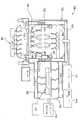
도 1은 일 실시예에 따른 HVPE 장치(100)의 개략적인 도면이며,
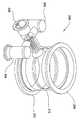
도 2는 다른 실시예에 따른 처리 챔버(200)의 개략적인 등축도이며,
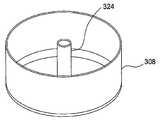
도 3a은 일 실시예에 따른 전구체 소오스(300)의 개략적인 횡단면도이며,
도 3b는 도 3a의 플로트의 개략적인 횡단면도이며,
도 3c는 도 3a의 플로트의 개략적인 저면도이며,
도 3d는 도 3a의 플로트의 개략적인 등축도이며,
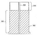
도 3e는 도 3a의 지지 라이너의 개략적인 횡단면도이며,
도 4a는 다른 실시예에 따른 전구체 소오스(400)의 개략적인 횡단면도이며,
도 4b는 도 4a의 샤워헤드의 개략적인 평면도이며,
도 4c는 도 4a의 샤워헤드의 개략적인 횡단면도이며,
도 4d는 도 4c의 샤워헤드의 상세도이며,
도 4e는 도 4a의 지지 라이너의 개략적인 횡단면도이다.Figure 1 is a schematic illustration of an
2 is a schematic isometric view of a
FIG. 3A is a schematic cross-sectional view of a
Figure 3b is a schematic cross-sectional view of the float of Figure 3a,
Figure 3c is a schematic bottom view of the float of Figure 3a,
Figure 3d is a schematic isometric view of the float of Figure 3a,
Figure 3e is a schematic cross-sectional view of the support liner of Figure 3a,
4A is a schematic cross-sectional view of a
Figure 4b is a schematic plan view of the showerhead of Figure 4a,
Figure 4c is a schematic cross-sectional view of the showerhead of Figure 4a,
FIG. 4D is a detailed view of the showerhead of FIG. 4C,
Figure 4e is a schematic cross-sectional view of the support liner of Figure 4a.
이해를 촉진시키기 위해, 도면들에 공통인 동일한 구성 요소들을 지칭하기 위해 가능한 한 동일한 도면 부호들이 사용되었다. 일 실시예에서 설명된 구성 요소들은 특별한 언급 없이도 다른 실시예들에 유리하게 사용될 수 있다고 이해해야 한다.
To facilitate understanding, the same reference numerals have been used, wherever possible, to designate identical elements that are common to the figures. It should be understood that the components described in one embodiment can be used advantageously in other embodiments without special mention.
본 명세서에 설명된 실시예들은 일반적으로 HVPE 챔버에 관한 것이다. 상기 챔버는 챔버에 연결된 하나 또는 그보다 많은 전구체 소오스들을 가질 수 있다. 두 개의 별도의 전구체 소오스들이 챔버에 연결될 때, 두 개의 별도의 층들이 증착될 수 있다. 예를 들어, 갈륨 소오스 및 별도의 알루미늄 소오스는 갈륨 질화물 및 알루미늄 질화물이 동일한 처리 챔버 내에 있는 기판 상에 별도로 증착될 수 있도록 처리 챔버에 연결될 수 있다. 일 실시예에서, 5 개의 전구체 소오스들이 챔버에 연결될 수 있다. 그와 같은 전구체 소오스들은 갈륨, 인듐, 알루미늄, 실리콘, 및 망간과 같은 전구체들을 분배할 수 있다. 전구체들이 질소 함유 화합물을 형성하는데 사용될 때, NH3와 같은 질소 함유 가스가 사용될 수 있다. 질소는 갈륨 및 알루미늄과 별개의 위치 및 더 낮은 온도에서 처리 챔버로 유입될 수 있다. 챔버의 형상은 전구체 및 반응 가스가 고 농도로 혼합되는 것을 방지하기 위해 별개로 챔버로 유입되도록 설정될 수 있다. 챔버 관성은 유동, 확산 및 대류에 의해 가스들을 혼합하도록 설계된다. 일 실시예에서, 상이한 온도들은 가스들이 챔버 벽들에는 전혀 또는 거의 증착되지 않으면서 서로 혼합, 반응하여 기판 상에 증착되는 것을 유발한다. 또한, 상기 챔버는 금속 산화물(MO) 소오스 배분 시스템을 갖추고 있다. 또한, 상기 챔버는 플라즈마 다운(down) 스트림, 가스 히터, 열선(hot wire) 등과 같은 활성 종 생성기를 갖추고 있다.
Embodiments described herein generally relate to an HVPE chamber. The chamber may have one or more precursor sources connected to the chamber. When two separate precursor sources are connected to the chamber, two separate layers can be deposited. For example, the gallium source and the separate aluminum source may be connected to the processing chamber such that gallium nitride and aluminum nitride may be deposited separately on the substrate in the same processing chamber. In one embodiment, five precursor sources may be connected to the chamber. Such precursor sources can distribute precursors such as gallium, indium, aluminum, silicon, and manganese. When precursors are used to form the nitrogen containing compound, a nitrogen containing gas such as NH3 may be used. Nitrogen can be introduced into the process chamber at a different location from gallium and aluminum and at lower temperatures. The shape of the chamber may be set to flow into the chamber separately to prevent the precursors and reaction gases from mixing at high concentrations. The chamber inertia is designed to mix gases by flow, diffusion and convection. In one embodiment, different temperatures cause gases to mix, react, and deposit on the substrate with little or no deposition on the chamber walls. The chamber also has a metal oxide (MO) source distribution system. The chamber also has an active species generator, such as a plasma down stream, a gas heater, a hot wire, and the like.
도 1은 일 실시예에 따른 HVPE 장치(100)의 개략도이다. 상기 장치(100)는 리드(104)에 의해 둘러싸인 챔버(102)를 포함한다. 제 1 가스 소오스(110)로부터의 처리 가스는 가스 분배 샤워헤드(106)를 통해 챔버(102)로 배분된다. 일 실시예에서, 가스 소오스(110)는 질소 함유 화합물을 포함할 수 있다. 다른 실시예에서, 가스 소오스(110)는 암모니아를 포함할 수 있다. 일 실시예에서, 헬륨 또는 이원자 질소와 같은 불활성 가스가 또한 가스 분배 샤워헤드(106) 또는 챔버(102)의 벽(108)을 통해 유입될 수 있다. 에너지 소오스(112)는 가스 소오스(110)와 가스 분배 샤워헤드(106) 사이에 배열될 수 있다. 일 실시예에서, 에너지 소오스(112)는 히터를 포함할 수 있다. 에너지 소오스(112)는 암모니아와 같은 가스 소오스(110)로부터의 가스를 붕괴시킴으로써, 질소 함유 가스로부터의 질소가 더욱 더 반응성이게 한다.
1 is a schematic diagram of an
제 1 소오스(110)로부터의 가스와 반응하기 위해, 전구체 재료가 하나 또는 그보다 많은 제 2 소오스(118)들로부터 배분될 수 있다. 하나 또는 그보다 많은 제 2 소오스(118)들은 갈륨 및 알루미늄과 같은 전구체들을 포함할 수 있다. 두 개의 전구체들을 참조할 것이지만, 상기에 논의된 바와 같이 다소간의 전구체들이 배분될 수 있다고 이해해야 한다. 일 실시예에서, 상기 전구체는 하나 또는 그보다 많은 제 2 소오스(118)들 내에 액체 형태로 존재하는 갈륨을 포함한다. 일 실시예에서, 하나 또는 그보다 많은 제 2 소오스(118)들 내에 존재하는 전구체는 액체 형태일 수 있다. 다른 실시예에서, 상기 전구체는 고체 형태 또는 고체 분말 형태로 하나 또는 그보다 많은 제 2 소오스들 내에 존재할 수 있다. 다른 실시예에서, 상기 전구체는 고체 형태로 전구체 소오스(118) 내에 존재하는 알루미늄을 포함한다. 일 실시예에서, 알루미늄 전구체는 고체 분말 형태일 수 있다. 상기 전구체는 전구체 소오스(118) 내의 전구체 위로 및/또는 전구체를 통해 반응 가스를 유동시킴으로써 챔버(102)로 배분될 수 있다. 일 실시예에서, 상기 반응 가스는 할로겐 가스를 포함할 수 있다. 일 실시예에서, 반응 가스는 이원자 염소와 같은 염소 함유 가스를 포함할 수 있다. 상기 염소 함유 가스는 염화물을 형성하기 위해 갈륨 또는 알루미늄과 같은 전구체 소오스와 반응할 수 있다. 일 실시예에서, 하나 또는 그보다 많은 제 2 소오스(118)들은 공정(eutectic) 재료들 및 그들의 합금들을 포함할 수 있다. 다른 실시예에서, HVPE 장치(100)는 도펀트 농도를 제어하기 위한 하나 이상의 고유한 소오스(intrinsic source)뿐만 아니라 도프된 소오스들을 처리하도록 배열될 수 있다.
In order to react with the gas from the
전구체와 반응하기 위한 염소 함유 가스의 효율을 증가시키기 위해, 염소 함유 가스는 챔버(132) 내의 보트(boat) 영역을 통해 유입되어 저항 히터(120)에 의해 가열될 수 있다. 염소 함유 가스가 챔버(132)를 통해 유입되는 체류 시간을 증가시킴으로써, 염소 함유 가스의 온도가 제어될 수 있다. 염소 함유 가스의 온도를 증가시킴으로써, 염소는 전구체와 더 빠르게 반응할 수 있다. 환언하면, 온도는 염소와 전구체 간의 반응에 촉매역할을 한다.
To increase the efficiency of the chlorine containing gas to react with the precursor, the chlorine containing gas may flow through the boat region in the
전구체의 반응성을 증가시키기 위해, 전구체는 보트 내의 제 2 챔버(132)에 있는 저항 히터(120)에 의해 가열될 수 있다. 예를 들어, 일 실시예에서 갈륨 전구체는 약 750 ℃ 내지 약 850 ℃ 범위의 온도로 가열될 수 있다. 염화물 반응 생성물은 그 후 챔버(102)로 배분될 수 있다. 반응성 염화물 생성물은 먼저 튜브(122)로 진입하여 튜브(122) 내에 균일하게 분포된다. 튜브(122)는 다른 튜브(124)에 연결된다. 염화물 반응 생성물은 제 1 튜브(122) 내에 균일하게 분포된 이후에 제 2 튜브(124)로 진입한다. 염화물 반응 생성물은 그 후 챔버(102) 내측으로 진입하며, 챔버에서 염화물 반응 생성물은 서셉터(114) 상에 배열된 기판(116) 상에 질화물 층을 형성하기 위해 질소 함유 가스와 혼합된다. 일 실시예에서, 서셉터(114)는 실리콘 탄화물을 포함할 수 있다. 상기 질화물 층은 예를 들어 갈륨 질화물 또는 알루미늄 질화물을 포함할 수 있다. 질소 및 염소와 같은 다른 반응 생성물은 배기구(126)를 통해 배기된다.
To increase the reactivity of the precursor, the precursor can be heated by the
챔버(102)는 부력 효과로 이어질 수 있는 열 구배를 가질 수 있다. 예를 들어, 질소계 가스가 약 450 ℃ 내지 약 550 ℃ 범위의 온도에서 가스 분배 샤워헤드(106)를 통해 유입된다. 챔버 벽(108)들은 약 600 ℃ 내지 약 700 ℃ 범위의 온도를 가질 수 있다. 서셉터(114)는 약 1050 ℃ 내지 1150 ℃ 범위의 온도를 가질 수 있다. 따라서, 챔버(102) 내의 온도차는 가열될 때에 챔버(102) 내에서 가스가 상승될 수 있게 하며 냉각될 때에 가스가 하락될 수 있게 한다. 가스의 상승 및 하락은 질소 가스와 염화물 가스의 혼합을 유발할 수 있다. 추가로, 부력 효과는 혼합으로 인해 벽(108)들 상에 증착되는 갈륨 질화물 또는 알루미늄 질화물의 양을 감소시킬 것이다.
The
처리 챔버(102)의 가열은 서셉터(114) 아래에 배열된 램프 모듈(128)로 서셉터(114)를 가열함으로써 수행된다. 증착 중, 램프 모듈(128)은 처리 챔버(102)를 위한 주요 열원이다. 램프 모듈(128)로서 도시되고 설명되지만, 다른 가열 소오스들이 사용될 수 있다고 이해해야 한다. 처리 챔버(102)의 추가의 가열은 챔버(102)의 벽(108)들 내에 매설된 히터(130)의 사용에 의해 수행될 수 있다. 벽(108)들 내에 매설된 히터(130)는 증착 공정 중에 거의 없는 열을 제공할 수 있다. 열전쌍(thermocouple)은 처리 챔버 내측의 온도를 측정하는데 사용될 수 있다. 열전쌍으로부터의 출력은 열전쌍으로부터 판독에 기초하여 히터(130)의 가열을 제어하는 제어기로 피드백될 수 있다. 예를 들어, 챔버가 너무 차가우면 히터(130)는 켜질 것이다. 챔버가 너무 뜨거우면 히터(130)는 꺼질 것이다. 추가로, 히터(130)로부터의 가열 양은 적은 양의 열이 히터(130)로부터 제공될 수 있도록 제어될 수 있다.
Heating of the
증착 공정 후에, 기판(116)은 처리 챔버(102)로부터 정상적으로 꺼내진다. 램프 모듈(128)은 꺼진다. 램프 모듈(128)로부터의 열 없이, 챔버(102)는 급속히 냉각될 수 있다. 벽(108)들 상에 증착될 수 있는 갈륨 질화물 또는 알루미늄 질화물은 벽(108)들 자체의 열팽창 계수와는 상이한 열팽창 계수를 가질 수 있다. 따라서, 갈륨 질화물 또는 알루미늄 질화물은 열팽창으로 인해 박리될 수 있다. 바람직하지 않은 박리를 방지하기 위해, 챔버 벽(108)들 내에 매설된 히터(130)는 열팽창를 제어하고 챔버(102)를 바람직한 챔버 온도로 유지하기 위해 켜질 수 있다. 히터(130)의 제어 또한, 열전쌍으로부터의 실시간 피드백을 기초로 할 수 있다. 일단 램프 모듈(128)이 꺼지면, 챔버(102)의 온도를 바람직한 온도로 유지하기 위해 히터(130)가 켜지거나 온도가 상승됨으로써 갈륨 질화물 또는 알루미늄 질화물이 박리되지 않고 기판을 오염시키지 않거나 서셉터(114)에 떨어지지 않으며 불균일한 서셉터(114) 표면을 형성하지도 않는다. 챔버 벽(108)들을 상승 온도로 유지함으로써, 염소가 챔버 벽(108)들로부터 증착물들을 세정하는데 더욱 효과적일 수 있다.
After the deposition process, the substrate 116 is normally removed from the
일반적으로, 증착 공정은 다음과 같이 진행될 것이다. 기판(116)이 먼저 처리 챔버(102) 내측에 삽입되며 서셉터(114) 상에 배열된다. 일 실시예에서, 기판(116)은 사파이어를 포함할 수 있다. 램프 모듈(128)은 기판(16) 및 대응적으로 챔버(102)를 가열하도록 켜질 수 있다. 질소 함유 반응 가스는 제 1 소오스(110)로부터 처리 챔버로 유입될 수 있다. 질소 함유 가스는 질소 함유 가스가 더욱더 반응성 상태가 되도록 가스 히터와 같은 에너지 소오스(112)를 통과할 수 있다. 질소 함유 가스는 그 후 챔버 리드(104)와 가스 분배 샤워헤드(106)를 통과한다. 일 실시예에서, 챔버 리드(104)는 수냉될 수 있다.
In general, the deposition process will proceed as follows. The substrate 116 is first inserted into the
전구체도 또한 챔버(102)로 배분될 수 있다. 염소 함유 가스는 전구체 소오스(118) 내의 전구체를 통해 및/또는 전구체 위로 통과할 수 있다. 염소 함유 가스는 그 후 염화물을 형성하도록 전구체와 반응한다. 염화물은 소오스 모듈(132) 내의 저항 히터(120)에 의해 가열된 후에 상부 튜브(122) 내측으로 배분되며 여기서 염화물은 튜브(122) 내에 균일하게 분배된다. 염화물 가스는 그 후 챔버(102)의 내측으로 유입되기 이전에 다른 튜브(124)로 흘러내린다. 염소 함유 가스가 논의되었지만, 본 발명은 염소 함유 가스에 한정되지 않는다고 이해해야 한다. 오히려, 다른 화합물들이 HVPE 공정에 사용될 수 있다. 챔버 벽(118)들은 벽(118)들 내에 매설된 히터(130)로부터 생성된 최소량의 열을 가질 수 있다. 챔버(120) 내의 대부분의 열은 서셉터(114) 아래에 있는 램프 모듈(128)에 의해 생성된다.
Precursors may also be dispensed into the
챔버(102) 내의 열 구배로 인해, 염화물 가스 및 질소 함유 가스는 처리 챔버(102) 내에서 상승 및 하락하며 그에 따라 기판(116) 상에 증착되는 질화물 화합물을 형성하도록 서로 혼합된다. 기판(116) 상의 증착 이외에도, 질화물 층은 챔버(102)의 다른 노출 영역들에도 또한 증착될 수 있다. 염화물 화합물 및 질소 함유 가스의 가스 반응 생성물은 진공 배기구(126)를 통해 챔버로부터 배기될 수 있는 질소 및 염소를 포함할 수 있다.
Due to the thermal gradient within the
일단 증착 공정이 완료되면, 램프 모듈(128)은 꺼지고 히터(130) 출력이 증가될 수 있다. 기판(116)은 제거될 수 있다. 히터(130) 출력은 열 팽창을 감소 또는 제거하며 그에 따라 소정의 세정 시간까지 임의의 증착된 질화물 재료를 제 위치에 유지하며 벽(108)들로부터 박리되지 않아 유입/출입 기판(116)의 서셉터(114) 상에 떨어지지 않는다. 일단 증착 공정이 완료되면, 벽(108)들 상에 증착된 임의의 질화물은 벽(108)들의 질화물을 에칭 제거하기 위한 에칭제를 유입함으로써 제거될 수 있다. 세정 중에, 램프 모듈(128)은 꺼질 수 있으며 대부분의 열은 벽(108)들 내에 매설된 히터(130)로부터 생성될 수 있다. 일단 새로운 기판(116)이 챔버(102) 내측에 놓이면, 상기 공정이 반복될 수 있다.
Once the deposition process is complete, the
질소 함유 가스가 가스 분배 샤워헤드(106)를 통해 도입되고 전구체가 챔버(102)의 중앙에 대응하는 영역으로 배분되는 것으로 논의되었지만, 가스 유입 위치는 역전될 수 있다고 이해해야 한다. 그러나, 전구체가 샤워헤드(106)를 통해 유입되면, 샤워헤드(106)는 염화물 반응 생성물의 반응성을 증가시키도록 가열될 수 있다.
It is to be understood that although the nitrogen containing gas is introduced through the
염화물 반응 생성물 및 암모니아가 상이한 온도들로 배분되기 때문에, 공동 공급부를 통한 암모니아 및 염화물 반응 생성물의 배분이 문제가 될 수 있다. 예를 들어, 석영 샤워헤드가 암모니아 및 염화물 반응 생성물 양쪽을 공급하는데 사용된다면, 석영 샤워헤드는 암모니아 및 염화물 반응 생성물의 상이한 온도들로 인해 균열이 생성될 수 있다.
Since the chloride reaction product and ammonia are distributed at different temperatures, the distribution of ammonia and chloride reaction products through the joint feed can be problematic. For example, if a quartz showerhead is used to supply both ammonia and chloride reaction products, the quartz showerhead may be cracked due to the different temperatures of the ammonia and chloride reaction products.
추가로, 증착 공정은 갈륨 질화물 층에 후속하여 사파이어 기판 상에 시이드 층(seed layer)으로서 얇은 알루미늄 질화물 층을 증착하는 단계를 수반할 수 있다. 갈륨 질화물 및 알루미늄 질화물 양쪽은 동일한 처리 챔버 내에서 증착될 수 있다. 그 후, 사파이어 기판은 제거되고 다른 층이 증착되는 MOCVD 처리 챔버 내에 놓일 수 있다. 몇몇 실시예들에서, 알루미늄 질화물 층은 제거될 수 있다. 알루미늄 질화물 층과 갈륨 질화물 층 양쪽이 동일한 챔버 내에서 증착되는 경우에, 임의의 다른 전구체가 염화물과 반응하여 염화물 반응 생성물을 형성하는 것을 방지하도록 이원자 질소의 역류가 사용될 수 있다. 이원자 질소는 염소가 다른 전구체와 접촉되게 유동될 수 있는 동안에는 반응되지 않는 전구체의 챔버 내측으로 유동될 수 있다. 따라서, 단지 하나의 전구체만이 한번에 반응하게 된다.
Additionally, the deposition process may involve depositing a thin aluminum nitride layer as a seed layer on the sapphire substrate following the gallium nitride layer. Both gallium nitride and aluminum nitride can be deposited in the same processing chamber. The sapphire substrate may then be removed and placed in an MOCVD processing chamber where another layer is deposited. In some embodiments, the aluminum nitride layer may be removed. Backflow of binary nitrogen may be used to prevent any other precursor from reacting with the chloride to form a chloride reaction product when both the aluminum nitride layer and the gallium nitride layer are deposited in the same chamber. The binary nitrogen may flow into the chamber of the unreacted precursor while the chlorine can flow in contact with the other precursor. Thus, only one precursor reacts at a time.
도 2는 다른 실시예에 따른 처리 챔버(200)의 개략적인 등축도이다. 상기 처리 챔버(200)는 제 1 전구체 소오스(202), 제 2 전구체 소오스(204), 반응 가스의 통행을 위한 통로(206), 상부 링(208), 하부 링(210), 및 측벽(212)들을 포함한다. 일 실시예에서, 상부 링(208) 및 하부 링(210)은 불투명한 석영을 포함한다. 일 실시예에서, 벽(212)들은 투명한 석영을 포함할 수 있다. 상기 링(208,210)들은 벽(212)들로부터 외측으로 연장하는 립(lip)들을 가질 수 있다. O-링들이 상기 립들의 에지의 외측에 배열될 수 있어서, O-링들이 가열된 챔버 벽(212)들 및 램프 모듈로부터 가능한 한 멀리 떨어지는 것을 보장한다. O-링들은 통상적으로, 약 250 ℃까지 사용될 수 있다. 그러므로, 챔버 몸체로부터 O-링들을 멀리 떨어지게 이동시키는 것이 유리하다.
2 is a schematic isometric view of a
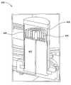
도 3a는 일 실시예에 따른 전구체 소오스(300)의 개략적인 횡단면도이다. 도 3b는 도 3a의 플로트의 개략적인 횡단면도이다. 도 3c는 도 3a의 플로트의 개략적인 저면도이다. 도 3d는 도 3a의 플로트 라이너의 개략적인 등축도이다. 도 3e는 도 3a의 지지 라이너의 개략적인 횡단면도이다. 본 발명에서 논의된 실시예에서, 전구체는 갈륨이었지만, 이러한 설명들은 임의의 액체 전구체에도 적용될 수 있는 것으로 이해해야 한다. 전구체 소오스(300)는 그 위에 플로트(304)를 갖는 전구체 자체를 포함할 수 있다. 플로트(304)는 염소 가스가 전구체와 접촉되도록 관통되게 유동시키는 항목이다. 플로트(304)는 지지 라이너(302) 상에 놓인 플로트 라이너(308) 위에 배열된다. 전구체는 플로트 라이너(308) 내에 배열된다. 도 3d에 도시된 바와 같이, 플로트 라이너(308)는 상방향으로 연장하는 벽(324)을 가진다. 플로트(304)는 내부에 통로를 갖는 플랜지(310)를 가지며, 플로트(304)가 플로트 라이너(308) 내측으로 가라앉을 때 상기 통로 내측으로 플로트 라이너(308)의 벽(324)이 연장한다. 플로트 라이너(308)의 벽(324)은 염소와 같은 반응 가스가 전구체 소오스(300)로 진입할 수 있도록 가스 통로를 둘러싼다. 일단 반응 가스가 전구체와 반응하면, 반응 생성물은 전구체 소오스(300)를 빠져나와 처리 챔버로 공급된다.
3A is a schematic cross-sectional view of a
일 실시예에서, 플로트(304)는 열분해 붕소 질화물(PBN: pyrolytic boron nitride)을 포함한다. 다른 실시예에서, 플로트(304)는 PBN-흑연을 포함한다. 다른 실시예에서, 플로트(304)는 흑연을 포함한다. 일 실시예에서, 플로트 라이너(308)는 PBN을 포함할 수 있다. 다른 실시예에서, 플로트 라이너(308)는 PBN-흑연을 포함할 수 있다. 다른 실시예에서, 플로트 라이너(308)는 흑연을 포함할 수 있다. 플로트(304)는 수직하게 상방향으로 연장하며 상기 플로트 라이너(308)의 바닥에 수직한 플랜지(310)를 가진다. 플로트(304)는 내부에 형성된 복수의 홈들을 가진다. 상기 홈들은 플로트(304)의 중앙 쪽으로 플로트(304)의 실질적인 에지로부터 반경 방향으로 연장하는 중앙 트렁크(trunk) 홈(312)을 포함한다. 복수의 원형 홈(314)들은 상기 중앙 트렁크 홈(312)으로부터 연장한다. 도 3b에 도시한 바와 같이, 상기 홈들은 반응 가스가 먼저 플랜지(310)를 통해 플로트(304)로 진입한 후에 상기 중앙 트렁크 홈(312) 및 원형 홈(314)들과 같은 홈들을 통해 분배되도록 플랜지(310)로 연장된다. 그 후 반응 생성물은 플로트(304)를 통해 형성된 개구(316)를 통해 전구체 소오스(300)를 이탈한다. 개구(316)는 플로트(304)의 실질적인 에지에 도시되어 있다.
In one embodiment,
염소와 같은 반응 가스가 전구체와 접촉하게 되면, 전구체의 일부가 사용될 것이다. 따라서, 액체의 레벨은 시간이 흐름에 따라 하강할 것이다. 그와 같이, 플로트(304)는 전구체 상에 떠 있으면서 아래로 이동할 것이며 그 결과로써 전구체에 대한 염소 가스의 노출은 전구체의 레벨이 하강하더라도 실질적으로 동일해진다. 플로트(304) 위의 영역(306)은 전구체가 감소함에 따라 증가할 수 있다. 플로트(304)용 재료들은 갈륨에 대한 석영 노출을 없애기 위한 PBN을 포함할 수 있다. 플로트(304)는 지지 라이너(302) 상에 놓이는 플로트 라이너(308) 내에 있는 전구체 상에 놓인다. 일 실시예에서, 지지 라이너(302)는 석영을 포함한다. 도 3e에 도시한 바와 같이, 지지 라이너(302)는 반응 가스가 통과하는 가스 관통 통로(322)를 가진다. 지지 라이너(302)는 플로트 라이너(308)가 내부에 놓이는 상부분(318) 및 하부분(320)을 가진다. 가스 통로(322)는 상부분(318) 및 하부분(320) 양쪽을 통해 연장한다. 플로트 라이너(308)의 벽(324)은 가스 통로(322)를 에워쌀 것이다. 따라서, 플로트(304)가 가라앉을 때 상기 벽(324)이 플로트(304)의 플랜지(310) 내측으로 연장할 뿐만 아니라 가스 통로(322)도 또한 플랜지(322)의 내측으로 연장할 것이다. 지지 라이너(302)와 같이, 상기 가스 통로(322)도 석영을 포함할 수 있다. 그러나, 가스 통로(322) 및 지지 라이너(302)가 단지, 염소와 같은 반응 가스에만 노출되고 액체 전구체에는 노출되지 않으므로, 석영은 이용하는 것이 용인될 수 있는 재료이다.
When a reactive gas, such as chlorine, comes into contact with the precursor, a portion of the precursor will be used. Thus, the level of liquid will drop over time. As such, the
일 실시예에서, 플로트(304)는 약 40 mm 내지 약 70 mm 범위의 전체 높이를 가진다. 플랜지(310)는 약 13 mm 내지 약 16 mm 범위의 내경을 가질 수 있다. 각각의 원형 홈(314)들은 반응 가스가 금속 소오스 전구체와의 접촉을 유지할 수 있게 하며 가스가 액체에 노출되는 체류 시간을 증가시킬 수 있게 한다. 플로트는 금속 전구체 상에 떠 있으며 따라서 금속 전구체의 레벨이 감소될 때 가라앉는다.
In one embodiment, the
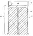
도 4a는 다른 실시예에 따른 전구체 소오스(400)의 개략적인 횡단면도이다. 도 4b는 도 4a의 샤워헤드의 개략적인 평면도이다. 도 4c는 도 4a의 샤워헤드의 개략적인 횡단면도이다. 도 4d는 도 4c의 샤워헤드의 상세도이다. 도 4e는 도 4a의 지지 라이너의 개략적인 횡단면도이다. 고체의 분말 알루미늄 전구체를 참조하여 설명하였지만, 상기 전구체는 임의의 고체 전구체일 수 있다고 이해해야 한다. 전구체는 샤워헤드(404) 아래에 있으며, 샤워헤드를 통해 염소 가스와 같은 반응 가스가 전구체와 접촉하도록 흐른다. 샤워헤드(404)는 염소 가스가 전구체에 노출되는 체류 시간을 증가시킴으로써 최적 양의 전구체가 처리 챔버로 배분될 수 있다. 샤워헤드(404)는 플로트가 아니기 때문에, 샤워헤드(404) 위의 영역(406)은 시간이 경과해도 증가하리라 예상되지 않는다. 샤워헤드(404)는 지지 라이너(402) 내에 놓인다.
4A is a schematic cross-sectional view of a
지지 라이너(402)는 하부분(410) 및 상부분(412)을 가진다. 일 실시예에서, 하부분(410)은 석영을 포함할 수 있다. 다른 실시예에서, 하부분(410)은 불투명한 석영을 포함할 수 있다. 일 실시예에서, 상부분(412)은 석영을 포함할 수 있다. 다른 실시예에서, 상부분(412)은 투명한 석영을 포함할 수 있다. 하부분(410)은 반응 가스 또는 반응 생성물이 통과하여 통행하기 위한 가스 통로(414)를 포함한다. 하부분(410)은 또한, 고체 전구체가 놓여 질 수 있는 공동(416)을 포함한다. 샤워헤드(404)는 전구체 소오스(400)가 조립될 때 렛지(ledge; 418) 상에 놓일 수 있다.
The
샤워헤드(404)는 복수의 동심 홈(420)들을 가진다. 각각의 홈(420)은 대응하는 홈(422)을 가진다. 상기 홈(420)들은 보다 작은 홈(422)들의 폭보다 큰 폭을 가진다. 각각의 홈(422) 내부에는, 샤워헤드 몸체를 통해 연장하는 복수의 가스 통로(424)들이 존재할 수 있다. 상기 가스 통로(424)들은 약 34도 내지 약 37도 범위만큼 이격되도록 최내측 홈(424A) 내에 배열될 수 있다. 다음 인접 홈(422B)을 위해, 가스 통로(424)들은 약 17도 내지 약 20도 범위만큼 이격될 수 있다. 다음 홈(422C)을 위해, 가스 통로(424)들은 약 11도 내지 약 14도 범위만큼 이격될 수 있다. 최외측 홈(422D)을 위해, 가스 통로(424)들은 약 8도 내지 약 11도 범위만큼 이격될 수 있다. 샤워헤드 몸체 내에 있는, 상기 홈(422)들을 위한 가스 통로(424)들은 모두 약 34도 내지 37도 간격으로 반경 방향으로 정렬된다. 홈(424B) 내의 모든 다른 가스 통로(424)는 홈(422A)을 위한 가스 통로(424)와 정렬된다. 홈(422C)의 모든 제 3 가스 통로(424)는 홈(422A) 내의 가스 통로(424)와 정렬된다. 최외측 홈(422D) 내의 모든 제 4 가스 통로(424)는 홈(422A) 내의 가스 통로(424)와 정렬된다.
The
일 실시예에서, 샤워헤드(404)는 세라믹 재료를 포함할 수 있다. 다른 실시예에서, 샤워헤드(404)는 알루미늄 산화물을 포함할 수 있다. 샤워헤드 몸체는 약 100 mm 내지 약 110 mm 범위의 직경을 가질 수 있다. 최외측 홈(420D), 제 3 홈(420C) 및 제 2 홈(420B)은 약 13 mm 내지 약 15 mm 범위의 폭을 가질 수 있다. 제 1 홈(420A)은 다른 홈(420B-D)들과 상이한 폭을 가질 수 있으며 약 18 mm 내지 약 21 mm 범위의 폭을 가질 수 있다. 샤워헤드(404)는 약 38 mm 내지 약 42 mm 범위의 전체 높이를 가질 수 있다. 각각의 홈(420)은 홈(420)들이 샤워헤드(404)의 바닥까지 완전히 연장하지 않도록 약 34 mm 내지 약 37 mm 범위의 높이를 가질 수 있다.
In one embodiment, the
본 명세서에서 논의된 실시예들은 챔버 벽에 부착되는 임의의 증착 필름들이 제조 기판 상의 결함들을 치유하기에 충분할 정도로 잘 부착되는 동시에, 벽 증착을 최소화한 고온 벽 HVPE CVD 반응로 설계에 관한 것이다. 상기 챔버는 두 개의 반응 가스들이 소정의 예열 온도들로 별도로 유입될 수 있도록 구성된다. 가스 주입은 두 개의 가스들이 벽으로부터 떨어져 대부분 혼합되나 이상적인 사전혼합을 보장하고 고 품질의 필름들을 제조하기에 충분한 확산 길이, 체적 및 부력을 제공하도록 설계되었다. 상기 장치는 샤워헤드 특징들을 포함하는 제어가능한 석영 또는 세라믹 벽들 및 독립형 히터에 의해 가열되는 다중 금속 소오스들을 포함한다. 상기 장치는 액체 및 고체 전구체들 양쪽을 수용할 수 있다.
The embodiments discussed herein relate to high temperature wall HVPE CVD reactor designs in which any deposition film deposited on the chamber walls is adhered well enough to heal defects on the fabrication substrate while minimizing wall deposition. The chamber is configured such that the two reaction gases can be separately introduced at predetermined preheat temperatures. Gas injection is designed to provide diffusion length, volume, and buoyancy sufficient to assure ideal premixing and to produce high quality films, although the two gases are mostly mixed off the wall. The apparatus includes controllable quartz or ceramic walls including showerhead features and multiple metal sources heated by a stand-alone heater. The apparatus can accommodate both liquid and solid precursors.
본 발명의 실시예들에 대해 설명하였지만, 본 발명의 다른 그리고 추가의 실시예들이 본 발명의 기본 범주로부터 이탈함이 없이 창안될 수 있으며, 본 발명의 범주는 이후의 특허청구범위에 의해 결정된다.
While embodiments of the invention have been described, other and further embodiments of the invention may be devised without departing from the basic scope thereof, and the scope of the invention is determined by the claims that follow .
Claims (15)
Translated fromKorean제 1 전구체 소오스, 및
제 2 전구체 소오스를 포함하는 수소화물 기상 에피택시(HVPE: hydride vapor phase epitaxy) 장치로서,
상기 제 1 전구체 소오스는 상기 진공 챔버 몸체에 인접 배열되고 상기 진공 챔버 몸체에 연결되며, 제 1 전구체 소오스 몸체, 상기 제 1 전구체 소오스 몸체 내에 배열되는 제 1 지지 라이너, 상기 제 1 지지 라이너에 연결되고 상기 제 1 전구체 소오스 몸체 내에 배열되는 플로트 라이너, 및 상기 제 1 전구체 소오스 몸체 내에 배열되며 상기 플로트 라이너로부터 제 1 거리만큼 떨어진 제 1 위치로부터 상기 플로트 라이너로부터 제 2 거리만큼 떨어진 제 2 위치로 이동할 수 있으며, 상기 제 1 거리는 상기 제 2 거리보다 큰 플로트를 포함하고,
상기 제 2 전구체 소오스는 상기 진공 챔버 몸체에 인접 배열되고 상기 진공 챔버 몸체에 연결되며, 상기 제 2 전구체 소오스는 상기 제 1 전구체 소오스로부터 분리되어 있는,
수소화물 기상 에피택시(HVPE) 장치.
Vacuum chamber body,
A first precursor source, and
A hydride vapor phase epitaxy (HVPE) device comprising a second precursor source,
The first precursor source is disposed adjacent to the vacuum chamber body and is connected to the vacuum chamber body and includes a first precursor source body, a first support liner arranged in the first precursor source body, a second support liner connected to the first support liner A float liner disposed in the first precursor source body and configured to move from a first position spaced a first distance from the float liner to a second position spaced a second distance from the float liner; Wherein the first distance comprises a float greater than the second distance,
Wherein the second precursor source is arranged adjacent to the vacuum chamber body and is connected to the vacuum chamber body and the second precursor source is separated from the first precursor source,
Hydride vapor phase epitaxy (HVPE) device.
상기 제 1 지지 라이너는 석영을 포함하는,
수소화물 기상 에피택시(HVPE) 장치.
The method according to claim 1,
Wherein the first support liner comprises quartz,
Hydride vapor phase epitaxy (HVPE) device.
상기 플로트 라이너는 열분해 붕소 질화물(pyrolytic boron nitride)을 포함하며, 상기 플로트는 열분해 붕소 질화물을 포함하는,
수소화물 기상 에피택시(HVPE) 장치.
3. The method of claim 2,
Wherein the float liner comprises pyrolytic boron nitride, the float comprising pyrolytic boron nitride,
Hydride vapor phase epitaxy (HVPE) device.
상기 플로트는 상기 플로트 라이너와 대면하는, 내부에 형성된 복수의 홈들을 가지며, 상기 복수의 홈들은
상기 플로트의 실질적인 에지(edge)로부터 반경 방향으로 연장하는 중앙 트렁크 홈, 및
상기 중앙 트렁크 홈으로부터 연장하는 하나 또는 그보다 많은 원형 홈들을 포함하는,
수소화물 기상 에피택시(HVPE) 장치.
The method according to claim 1,
Wherein the float has a plurality of grooves formed therein facing the float liner, the plurality of grooves
A central trunk groove extending radially from a substantial edge of the float, and
And one or more circular grooves extending from the central trunk groove.
Hydride vapor phase epitaxy (HVPE) device.
상기 플로트 라이너는 상기 플로트 라이너의 바닥 표면에 실질적으로 수직하게 연장하는 중앙 벽을 포함하며, 상기 플로트는 상기 플로트 라이너의 중앙 벽에 실질적으로 평행하게 연장하는 중앙 플랜지를 포함하며, 상기 플로트 라이너의 중앙 벽은 상기 플로트의 중앙 플랜지 내에 배열되는,
수소화물 기상 에피택시(HVPE) 장치.
The method according to claim 1,
Wherein the float liner comprises a central wall extending substantially perpendicular to a bottom surface of the float liner, the float including a central flange extending substantially parallel to a center wall of the float liner, A wall is arranged in the central flange of the float,
Hydride vapor phase epitaxy (HVPE) device.
제 1 전구체 소오스, 및
제 2 전구체 소오스를 포함하는 수소화물 기상 에피택시(HVPE) 장치로서,
상기 제 1 전구체 소오스는 상기 진공 챔버 몸체에 인접 배열되고 상기 진공 챔버 몸체에 연결되며, 제 1 전구체 소오스 몸체, 상기 제 1 전구체 소오스 몸체 내에 배열되는 제 1 지지 라이너, 및 상기 제 1 전구체 소오스 몸체 내에 배열되고 상기 제 1 지지 라이너에 연결되는 샤워헤드를 포함하고,
상기 제 2 전구체 소오스는 상기 진공 챔버 몸체에 인접 배열되고 상기 진공 챔버 몸체에 연결되며, 상기 제 2 전구체 소오스는 상기 제 1 전구체 소오스로부터 분리되어 있는,
수소화물 기상 에피택시(HVPE) 장치.
Vacuum chamber body,
A first precursor source, and
A hydride vapor phase epitaxy (HVPE) device comprising a second precursor source,
The first precursor source is disposed adjacent to the vacuum chamber body and is connected to the vacuum chamber body and includes a first precursor source body, a first support liner arranged in the first precursor source body, and a second precursor source body disposed in the first precursor source body And a showerhead arranged and connected to the first support liner,
Wherein the second precursor source is arranged adjacent to the vacuum chamber body and is connected to the vacuum chamber body and the second precursor source is separated from the first precursor source,
Hydride vapor phase epitaxy (HVPE) device.
상기 제 1 지지 라이너는 석영을 포함하며 상기 샤워헤드는 세라믹 재료를 포함하는,
수소화물 기상 에피택시(HVPE) 장치.
The method according to claim 6,
Wherein the first support liner comprises quartz and the showerhead comprises a ceramic material.
Hydride vapor phase epitaxy (HVPE) device.
상기 샤워헤드는 각각 제 1 폭을 갖는, 내부에 형성된 복수의 제 1 원형 홈들을 구비한 샤워헤드 몸체를 포함하며, 상기 샤워헤드 몸체의 제 1 홈 각각은 상기 제 1 폭보다 작은 제 2 폭을 갖는, 내부에 형성된 제 2 홈을 가지며, 상기 샤워헤드 몸체는 상기 제 2 홈으로부터 샤워헤드 몸체를 통해 연장하는 하나 또는 그보다 많은 개구들을 가지는,
수소화물 기상 에피택시(HVPE) 장치.
The method according to claim 6,
Wherein the showerhead comprises a showerhead body having a first plurality of circular grooves formed therein having a first width, each of the first grooves of the showerhead body having a second width less than the first width Wherein the shower head body has one or more openings extending through the showerhead body from the second groove,
Hydride vapor phase epitaxy (HVPE) device.
제 1 전구체 소오스, 및
제 2 전구체 소오스를 포함하며,
상기 제 1 전구체 소오스는 상기 진공 챔버 몸체에 인접 배열되고 상기 진공 챔버 몸체에 연결되며, 제 1 전구체 소오스 몸체, 상기 제 1 전구체 소오스 몸체 내에 배열되는 제 1 지지 라이너, 상기 제 1 지지 라이너에 연결되고 상기 제 1 전구체 소오스 몸체 내에 배열되는 플로트 라이너, 및 상기 제 1 전구체 소오스 몸체 내에 배열되며 상기 플로트 라이너로부터 제 1 거리만큼 떨어진 제 1 위치로부터 상기 플로트 라이너로부터 제 2 거리만큼 떨어진 제 2 위치로 이동할 수 있으며, 상기 제 1 거리는 상기 제 2 거리보다 큰 플로트를 포함하고,
상기 제 2 전구체 소오스는 상기 진공 챔버 몸체에 인접 배열되고 상기 진공 챔버 몸체에 연결되며, 상기 제 2 전구체 소오스는 상기 제 1 전구체 소오스로부터 분리되어 있으며, 제 2 전구체 소오스 몸체, 상기 제 1 전구체 소오스 몸체 내에 배열되는 제 2 지지 라이너, 및 상기 제 1 전구체 소오스 몸체 내에 배열되고 상기 제 1 지지 라이너에 연결되는 샤워헤드를 포함하는,
수소화물 기상 에피택시(HVPE) 장치.
Vacuum chamber body,
A first precursor source, and
A second precursor source,
The first precursor source is disposed adjacent to the vacuum chamber body and is connected to the vacuum chamber body and includes a first precursor source body, a first support liner arranged in the first precursor source body, a second support liner connected to the first support liner A float liner disposed in the first precursor source body and configured to move from a first position spaced a first distance from the float liner to a second position spaced a second distance from the float liner; Wherein the first distance comprises a float greater than the second distance,
The second precursor source is disposed adjacent to the vacuum chamber body and is connected to the vacuum chamber body. The second precursor source is separated from the first precursor source, and the second precursor source, the first precursor source body, And a showerhead arranged in the first precursor source body and connected to the first support liner,
Hydride vapor phase epitaxy (HVPE) device.
상기 제 1 지지 라이너는 석영을 포함하며, 상기 플로트 라이너는 열분해 붕소 질화물을 포함하며, 상기 플로트는 열분해 붕소 질화물을 포함하는,
수소화물 기상 에피택시(HVPE) 장치.
10. The method of claim 9,
Said first support liner comprising quartz, said float liner comprising pyrolytic boron nitride, said float comprising pyrolytic boron nitride,
Hydride vapor phase epitaxy (HVPE) device.
상기 플로트는 상기 플로트 라이너와 대면하는, 내부에 형성된 복수의 홈들을 가지는,
수소화물 기상 에피택시(HVPE) 장치.
10. The method of claim 9,
The float having a plurality of grooves formed therein, facing the float liner,
Hydride vapor phase epitaxy (HVPE) device.
상기 복수의 홈들은
상기 플로트의 실질적인 에지로부터 반경 방향으로 연장하는 중앙 트렁크 홈, 및
상기 중앙 트렁크 홈으로부터 연장하는 하나 또는 그보다 많은 원형 홈들을 포함하는,
수소화물 기상 에피택시(HVPE) 장치.
12. The method of claim 11,
The plurality of grooves
A central trunk groove extending radially from a substantial edge of the float, and
And one or more circular grooves extending from the central trunk groove.
Hydride vapor phase epitaxy (HVPE) device.
상기 플로트 라이너는 상기 플로트 라이너의 바닥 표면에 실질적으로 수직하게 연장하는 중앙 벽을 포함하며, 상기 플로트는 상기 플로트 라이너의 중앙 벽에 실질적으로 평행하게 연장하는 중앙 플랜지를 포함하며, 상기 플로트 라이너의 중앙 벽은 상기 플로트의 중앙 플랜지 내에 배열되는,
수소화물 기상 에피택시(HVPE) 장치.
13. The method of claim 12,
Wherein the float liner comprises a central wall extending substantially perpendicular to a bottom surface of the float liner, the float including a central flange extending substantially parallel to a center wall of the float liner, A wall is arranged in the central flange of the float,
Hydride vapor phase epitaxy (HVPE) device.
상기 제 1 지지 라이너는 석영을 포함하며 상기 샤워헤드는 세라믹 재료를 포함하는,
수소화물 기상 에피택시(HVPE) 장치.
10. The method of claim 9,
Wherein the first support liner comprises quartz and the showerhead comprises a ceramic material.
Hydride vapor phase epitaxy (HVPE) device.
상기 샤워헤드는 각각 제 1 폭을 갖는, 내부에 형성된 복수의 제 1 원형 홈들을 구비한 샤워헤드 몸체를 포함하며, 상기 샤워헤드 몸체의 제 1 홈 각각은 상기 제 1 폭보다 작은 제 2 폭을 갖는, 내부에 형성된 제 2 홈을 가지며, 상기 샤워헤드 몸체는 상기 제 2 홈으로부터 샤워헤드 몸체를 통해 연장하는 하나 또는 그보다 많은 개구들을 가지는,
수소화물 기상 에피택시(HVPE) 장치.
10. The method of claim 9,
Wherein the showerhead comprises a showerhead body having a first plurality of circular grooves formed therein having a first width, each of the first grooves of the showerhead body having a second width less than the first width Wherein the shower head body has one or more openings extending through the showerhead body from the second groove,
Hydride vapor phase epitaxy (HVPE) device.
Applications Claiming Priority (9)
| Application Number | Priority Date | Filing Date | Title |
|---|---|---|---|
| US16839909P | 2009-04-10 | 2009-04-10 | |
| US61/168,399 | 2009-04-10 | ||
| US17263009P | 2009-04-24 | 2009-04-24 | |
| US61/172,630 | 2009-04-24 | ||
| US23087709P | 2009-08-03 | 2009-08-03 | |
| US61/230,877 | 2009-08-03 | ||
| US12/637,028 | 2009-12-14 | ||
| US12/637,028US8491720B2 (en) | 2009-04-10 | 2009-12-14 | HVPE precursor source hardware |
| PCT/US2010/030496WO2010118295A2 (en) | 2009-04-10 | 2010-04-09 | Hvpe precursor source hardware |
Publications (2)
| Publication Number | Publication Date |
|---|---|
| KR20120006542A KR20120006542A (en) | 2012-01-18 |
| KR101665304B1true KR101665304B1 (en) | 2016-10-12 |
Family
ID=42933312
Family Applications (2)
| Application Number | Title | Priority Date | Filing Date |
|---|---|---|---|
| KR1020117026834AActiveKR101690056B1 (en) | 2009-04-10 | 2010-04-09 | HVPE chamber hardware |
| KR1020117026829AActiveKR101665304B1 (en) | 2009-04-10 | 2010-04-09 | HVPE precursor source hardware |
Family Applications Before (1)
| Application Number | Title | Priority Date | Filing Date |
|---|---|---|---|
| KR1020117026834AActiveKR101690056B1 (en) | 2009-04-10 | 2010-04-09 | HVPE chamber hardware |
Country Status (5)
| Country | Link |
|---|---|
| US (2) | US8491720B2 (en) |
| KR (2) | KR101690056B1 (en) |
| CN (3) | CN102414792B (en) |
| TW (3) | TWD138506S1 (en) |
| WO (2) | WO2010118293A2 (en) |
Families Citing this family (15)
| Publication number | Priority date | Publication date | Assignee | Title |
|---|---|---|---|---|
| US8491720B2 (en)* | 2009-04-10 | 2013-07-23 | Applied Materials, Inc. | HVPE precursor source hardware |
| CN102766902B (en)* | 2011-05-05 | 2015-12-02 | 北京北方微电子基地设备工艺研究中心有限责任公司 | Processing chamber device and the substrate processing equipment with this processing chamber device |
| US9303318B2 (en)* | 2011-10-20 | 2016-04-05 | Applied Materials, Inc. | Multiple complementary gas distribution assemblies |
| CN103014846A (en)* | 2013-01-14 | 2013-04-03 | 东莞市中镓半导体科技有限公司 | A Concentric Ring Nozzle Structure for Material Vapor Phase Epitaxy |
| US9327252B2 (en) | 2013-03-15 | 2016-05-03 | Applied Materials, Inc. | Compact device for enhancing the mixing of gaseous species |
| US9373529B2 (en)* | 2013-10-23 | 2016-06-21 | Taiwan Semiconductor Manufacturing Company, Ltd. | Process tool having third heating source and method of using the same |
| USD767112S1 (en)* | 2015-04-15 | 2016-09-20 | K&N Engineering, Inc. | Vent breather |
| JP6565502B2 (en)* | 2015-09-03 | 2019-08-28 | 株式会社島津製作所 | Film forming apparatus and film forming method |
| CN117265507A (en)* | 2016-11-11 | 2023-12-22 | 优材科技有限公司 | Heater module, thin film deposition apparatus and thin film deposition method |
| KR102165760B1 (en)* | 2018-02-12 | 2020-10-14 | 전주대학교 산학협력단 | Hydride Vapour Phase Epitaxy Reactor |
| CN109468680A (en)* | 2018-12-19 | 2019-03-15 | 东莞市中镓半导体科技有限公司 | A kind of gas preheating unit applied to hydride gas-phase epitaxy equipment |
| US12091749B2 (en) | 2021-05-11 | 2024-09-17 | Applied Materials, Inc. | Method for epitaxially depositing a material on a substrate by flowing a process gas across the substrate from an upper gas inlet to an upper gas outlet and flowing a purge gas from a lower gas inlet to a lower gas outlet |
| US12018372B2 (en) | 2021-05-11 | 2024-06-25 | Applied Materials, Inc. | Gas injector for epitaxy and CVD chamber |
| US12060651B2 (en) | 2021-05-11 | 2024-08-13 | Applied Materials, Inc. | Chamber architecture for epitaxial deposition and advanced epitaxial film applications |
| CN114807886B (en)* | 2022-04-13 | 2024-05-17 | 北京北方华创微电子装备有限公司 | Process chamber and process method |
Citations (3)
| Publication number | Priority date | Publication date | Assignee | Title |
|---|---|---|---|---|
| JP2006120857A (en) | 2004-10-21 | 2006-05-11 | Hitachi Cable Ltd | Vapor growth apparatus, semiconductor substrate manufacturing method using the same, and semiconductor substrate |
| JP2007039272A (en) | 2005-08-03 | 2007-02-15 | Furukawa Co Ltd | Hydride vapor growth system, method for producing group iii nitride semiconductor substrate and group iii nitride semiconductor substrate |
| US20080276860A1 (en) | 2007-05-10 | 2008-11-13 | Burrows Brian H | Cross flow apparatus and method for hydride vapor phase deposition |
Family Cites Families (129)
| Publication number | Priority date | Publication date | Assignee | Title |
|---|---|---|---|---|
| US3063867A (en) | 1958-12-16 | 1962-11-13 | Western Electric Co | Deposition and measurement of layer thickness |
| US4286436A (en)* | 1980-06-16 | 1981-09-01 | Chicago Bridge & Iron Company | Falling film freeze exchanger |
| US4851295A (en)* | 1984-03-16 | 1989-07-25 | Genus, Inc. | Low resistivity tungsten silicon composite film |
| US4750975A (en)* | 1986-03-17 | 1988-06-14 | Uni-Frac, Inc. | Vapor/liquid contact column structure |
| US5037624A (en)* | 1987-03-24 | 1991-08-06 | Advanced Technology Materials Inc. | Composition, apparatus, and process, for sorption of gaseous compounds of group II-VII elements |
| US5348911A (en)* | 1987-06-30 | 1994-09-20 | Aixtron Gmbh | Material-saving process for fabricating mixed crystals |
| USD329839S (en)* | 1990-01-31 | 1992-09-29 | Hohner Automation Societe Anonyme | Incremental coder |
| WO1992022084A1 (en)* | 1991-05-21 | 1992-12-10 | Advantage Production Technology, Inc. | Organic preclean for improving vapor phase wafer etch uniformity |
| US5273588A (en) | 1992-06-15 | 1993-12-28 | Materials Research Corporation | Semiconductor wafer processing CVD reactor apparatus comprising contoured electrode gas directing means |
| US5647911A (en) | 1993-12-14 | 1997-07-15 | Sony Corporation | Gas diffuser plate assembly and RF electrode |
| US5359788A (en)* | 1993-12-22 | 1994-11-01 | Gell Jr Harold A | Coffee roaster |
| US5679152A (en)* | 1994-01-27 | 1997-10-21 | Advanced Technology Materials, Inc. | Method of making a single crystals Ga*N article |
| WO1995027570A1 (en)* | 1994-04-08 | 1995-10-19 | Ray Mark A | Selective plasma deposition |
| GB9411911D0 (en)* | 1994-06-14 | 1994-08-03 | Swan Thomas & Co Ltd | Improvements in or relating to chemical vapour deposition |
| US5715361A (en)* | 1995-04-13 | 1998-02-03 | Cvc Products, Inc. | Rapid thermal processing high-performance multizone illuminator for wafer backside heating |
| US5636320A (en) | 1995-05-26 | 1997-06-03 | International Business Machines Corporation | Sealed chamber with heating lamps provided within transparent tubes |
| JPH0945670A (en)* | 1995-07-29 | 1997-02-14 | Hewlett Packard Co <Hp> | Vapor phase etching method of group iiinitrogen crystal and re-deposition process method |
| US5827427A (en)* | 1996-03-11 | 1998-10-27 | Kinetico Incorporated | Tank assembly |
| US5667592A (en)* | 1996-04-16 | 1997-09-16 | Gasonics International | Process chamber sleeve with ring seals for isolating individual process modules in a common cluster |
| US6533874B1 (en)* | 1996-12-03 | 2003-03-18 | Advanced Technology Materials, Inc. | GaN-based devices using thick (Ga, Al, In)N base layers |
| US5855675A (en)* | 1997-03-03 | 1999-01-05 | Genus, Inc. | Multipurpose processing chamber for chemical vapor deposition processes |
| US6286451B1 (en) | 1997-05-29 | 2001-09-11 | Applied Materials, Inc. | Dome: shape and temperature controlled surfaces |
| US6270569B1 (en)* | 1997-06-11 | 2001-08-07 | Hitachi Cable Ltd. | Method of fabricating nitride crystal, mixture, liquid phase growth method, nitride crystal, nitride crystal powders, and vapor phase growth method |
| US6527865B1 (en)* | 1997-09-11 | 2003-03-04 | Applied Materials, Inc. | Temperature controlled gas feedthrough |
| US6254772B1 (en)* | 1998-01-15 | 2001-07-03 | Yiu Chau Chau | Backwashable filtration system |
| US6464843B1 (en) | 1998-03-31 | 2002-10-15 | Lam Research Corporation | Contamination controlling method and apparatus for a plasma processing chamber |
| US6086673A (en)* | 1998-04-02 | 2000-07-11 | Massachusetts Institute Of Technology | Process for producing high-quality III-V nitride substrates |
| US6101816A (en)* | 1998-04-28 | 2000-08-15 | Advanced Technology Materials, Inc. | Fluid storage and dispensing system |
| WO1999066565A1 (en) | 1998-06-18 | 1999-12-23 | University Of Florida | Method and apparatus for producing group-iii nitrides |
| US6190732B1 (en)* | 1998-09-03 | 2001-02-20 | Cvc Products, Inc. | Method and system for dispensing process gas for fabricating a device on a substrate |
| US6413839B1 (en)* | 1998-10-23 | 2002-07-02 | Emcore Corporation | Semiconductor device separation using a patterned laser projection |
| US6373114B1 (en)* | 1998-10-23 | 2002-04-16 | Micron Technology, Inc. | Barrier in gate stack for improved gate dielectric integrity |
| KR100304664B1 (en)* | 1999-02-05 | 2001-09-26 | 윤종용 | Method for fabricating a GaN film |
| US6309465B1 (en) | 1999-02-18 | 2001-10-30 | Aixtron Ag. | CVD reactor |
| US6200893B1 (en)* | 1999-03-11 | 2001-03-13 | Genus, Inc | Radical-assisted sequential CVD |
| US6540838B2 (en)* | 2000-11-29 | 2003-04-01 | Genus, Inc. | Apparatus and concept for minimizing parasitic chemical vapor deposition during atomic layer deposition |
| US6305314B1 (en) | 1999-03-11 | 2001-10-23 | Genvs, Inc. | Apparatus and concept for minimizing parasitic chemical vapor deposition during atomic layer deposition |
| US6179913B1 (en)* | 1999-04-16 | 2001-01-30 | Cbl Technologies, Inc. | Compound gas injection system and methods |
| US6413860B1 (en)* | 1999-04-27 | 2002-07-02 | Tokyo Electron Limited | PECVD of Ta films from tanatalum halide precursors |
| US6268288B1 (en)* | 1999-04-27 | 2001-07-31 | Tokyo Electron Limited | Plasma treated thermal CVD of TaN films from tantalum halide precursors |
| US6265311B1 (en)* | 1999-04-27 | 2001-07-24 | Tokyo Electron Limited | PECVD of TaN films from tantalum halide precursors |
| US6410433B1 (en)* | 1999-04-27 | 2002-06-25 | Tokyo Electron Limited | Thermal CVD of TaN films from tantalum halide precursors |
| US6410432B1 (en)* | 1999-04-27 | 2002-06-25 | Tokyo Electron Limited | CVD of integrated Ta and TaNx films from tantalum halide precursors |
| EP1115147A4 (en) | 1999-05-26 | 2007-05-02 | Tadahiro Ohmi | PLASMA TREATMENT DEVICE |
| US6206972B1 (en)* | 1999-07-08 | 2001-03-27 | Genus, Inc. | Method and apparatus for providing uniform gas delivery to substrates in CVD and PECVD processes |
| US6444038B1 (en)* | 1999-12-27 | 2002-09-03 | Morton International, Inc. | Dual fritted bubbler |
| US6569765B1 (en)* | 1999-08-26 | 2003-05-27 | Cbl Technologies, Inc | Hybrid deposition system and methods |
| US6489241B1 (en) | 1999-09-17 | 2002-12-03 | Applied Materials, Inc. | Apparatus and method for surface finishing a silicon film |
| US6998152B2 (en)* | 1999-12-20 | 2006-02-14 | Micron Technology, Inc. | Chemical vapor deposition methods utilizing ionic liquids |
| US6503330B1 (en) | 1999-12-22 | 2003-01-07 | Genus, Inc. | Apparatus and method to achieve continuous interface and ultrathin film during atomic layer deposition |
| US6897119B1 (en)* | 1999-12-22 | 2005-05-24 | Genus, Inc. | Apparatus and method to achieve continuous interface and ultrathin film during atomic layer deposition |
| US6551399B1 (en) | 2000-01-10 | 2003-04-22 | Genus Inc. | Fully integrated process for MIM capacitors using atomic layer deposition |
| KR100780143B1 (en)* | 2000-02-04 | 2007-11-27 | 아익스트론 아게 | Apparatus and methods for depositing one or more layers on a substrate |
| US6743473B1 (en)* | 2000-02-16 | 2004-06-01 | Applied Materials, Inc. | Chemical vapor deposition of barriers from novel precursors |
| US6517634B2 (en) | 2000-02-28 | 2003-02-11 | Applied Materials, Inc. | Chemical vapor deposition chamber lid assembly |
| US6475902B1 (en)* | 2000-03-10 | 2002-11-05 | Applied Materials, Inc. | Chemical vapor deposition of niobium barriers for copper metallization |
| JP4849705B2 (en)* | 2000-03-24 | 2012-01-11 | 東京エレクトロン株式会社 | Plasma processing apparatus, plasma generation introducing member, and dielectric |
| ATE518239T1 (en) | 2000-04-17 | 2011-08-15 | Mattson Tech Inc | METHOD FOR UV PRETREATMENT OF ULTRATHIN OXYNITRIDE FOR PRODUCING SILICON NITRIDE LAYERS |
| DE60106675T2 (en)* | 2000-05-31 | 2005-12-01 | Shipley Co., L.L.C., Marlborough | Evaporator |
| US6837251B1 (en)* | 2000-06-21 | 2005-01-04 | Air Products And Chemicals, Inc. | Multiple contents container assembly for ultrapure solvent purging |
| US6440495B1 (en)* | 2000-08-03 | 2002-08-27 | Applied Materials, Inc. | Chemical vapor deposition of ruthenium films for metal electrode applications |
| JP5095064B2 (en)* | 2000-08-04 | 2012-12-12 | ザ リージェンツ オブ ザ ユニバーシティ オブ カリフォルニア | Semiconductor film having nitride layer deposited on silicon substrate and method for manufacturing the same |
| US6616870B1 (en) | 2000-08-07 | 2003-09-09 | Shipley Company, L.L.C. | Method of producing high aspect ratio domes by vapor deposition |
| DE10043601A1 (en) | 2000-09-01 | 2002-03-14 | Aixtron Ag | Device and method for depositing, in particular, crystalline layers on, in particular, crystalline substrates |
| JP4374156B2 (en)* | 2000-09-01 | 2009-12-02 | 日本碍子株式会社 | III-V Group Nitride Film Manufacturing Apparatus and Manufacturing Method |
| DE10048759A1 (en) | 2000-09-29 | 2002-04-11 | Aixtron Gmbh | Method and device for separating organic layers in particular by means of OVPD |
| DE10056029A1 (en) | 2000-11-11 | 2002-05-16 | Aixtron Ag | Controlling surface temperature of substrates supported by carriers on dynamic gas cushions in process chamber of CVD reactor comprises varying gas stream producing gas cushions from average value of optically measured surface temperatures |
| DE10057134A1 (en) | 2000-11-17 | 2002-05-23 | Aixtron Ag | Process for depositing crystalline layers onto crystalline substrates in a process chamber of a CVD reactor comprises adjusting the kinematic viscosity of the carrier gas mixed |
| US6905547B1 (en)* | 2000-12-21 | 2005-06-14 | Genus, Inc. | Method and apparatus for flexible atomic layer deposition |
| US7348042B2 (en)* | 2001-03-19 | 2008-03-25 | Novellus Systems, Inc. | Continuous method for depositing a film by modulated ion-induced atomic layer deposition (MII-ALD) |
| US6656272B2 (en) | 2001-03-30 | 2003-12-02 | Technologies And Devices International, Inc. | Method of epitaxially growing submicron group III nitride layers utilizing HVPE |
| DE10118130A1 (en) | 2001-04-11 | 2002-10-17 | Aixtron Ag | Device for depositing crystalline layers on crystalline substrates in the gas phase comprises a heated reaction chamber with substrate holders arranged in a circular manner on a support, heated sources, and a hydride feed line |
| DE10124609B4 (en) | 2001-05-17 | 2012-12-27 | Aixtron Se | Method for depositing active layers on substrates |
| US20030205193A1 (en)* | 2001-07-06 | 2003-11-06 | Melnik Yuri V. | Method for achieving low defect density aigan single crystal boules |
| US7501023B2 (en)* | 2001-07-06 | 2009-03-10 | Technologies And Devices, International, Inc. | Method and apparatus for fabricating crack-free Group III nitride semiconductor materials |
| US6648966B2 (en) | 2001-08-01 | 2003-11-18 | Crystal Photonics, Incorporated | Wafer produced thereby, and associated methods and devices using the wafer |
| US6756318B2 (en)* | 2001-09-10 | 2004-06-29 | Tegal Corporation | Nanolayer thick film processing system and method |
| US20030111473A1 (en)* | 2001-10-12 | 2003-06-19 | Polymer & Steel Technologies Holding Company, L.L.C. | Composite pressure vessel assembly and method |
| TW200300701A (en)* | 2001-11-30 | 2003-06-16 | Asml Us Inc | High flow rate bubbler system and method |
| JP2006512748A (en)* | 2001-12-21 | 2006-04-13 | アイクストロン、アーゲー | Method for depositing a III-V semiconductor film on a non-III-V substrate |
| DE10163394A1 (en)* | 2001-12-21 | 2003-07-03 | Aixtron Ag | Method and device for depositing crystalline layers and on crystalline substrates |
| US6620225B2 (en)* | 2002-01-10 | 2003-09-16 | Advanced Technology Materials, Inc. | Adsorbents for low vapor pressure fluid storage and delivery |
| US6969426B1 (en)* | 2002-02-26 | 2005-11-29 | Bliss David F | Forming improved metal nitrides |
| US20050239675A1 (en)* | 2002-04-01 | 2005-10-27 | Munzer Makansi | Carrier foam to enhance liquid functional performance |
| US20030192430A1 (en)* | 2002-04-11 | 2003-10-16 | Pearlstein Ronald Martin | Helical built-in purifier for gas supply cylinders |
| CN1324772C (en)* | 2002-06-19 | 2007-07-04 | 日本电信电话株式会社 | Semiconductor light-emitting device |
| US6921062B2 (en)* | 2002-07-23 | 2005-07-26 | Advanced Technology Materials, Inc. | Vaporizer delivery ampoule |
| JP4352783B2 (en) | 2002-08-23 | 2009-10-28 | 東京エレクトロン株式会社 | Gas supply system and processing system |
| US7115896B2 (en) | 2002-12-04 | 2006-10-03 | Emcore Corporation | Semiconductor structures for gallium nitride-based devices |
| US6911065B2 (en)* | 2002-12-26 | 2005-06-28 | Matheson Tri-Gas, Inc. | Method and system for supplying high purity fluid |
| US7018940B2 (en) | 2002-12-30 | 2006-03-28 | Genus, Inc. | Method and apparatus for providing uniform gas delivery to substrates in CVD and PECVD processes |
| JP4026529B2 (en)* | 2003-04-10 | 2007-12-26 | 東京エレクトロン株式会社 | Shower head structure and processing apparatus |
| US7172646B2 (en)* | 2003-04-15 | 2007-02-06 | Air Products And Chemicals, Inc. | Reactive liquid based gas storage and delivery systems |
| US6921437B1 (en) | 2003-05-30 | 2005-07-26 | Aviza Technology, Inc. | Gas distribution system |
| US7170095B2 (en)* | 2003-07-11 | 2007-01-30 | Cree Inc. | Semi-insulating GaN and method of making the same |
| US7156380B2 (en)* | 2003-09-29 | 2007-01-02 | Asm International, N.V. | Safe liquid source containers |
| DE102004009130A1 (en)* | 2004-02-25 | 2005-09-15 | Aixtron Ag | Inlet system for a MOCVD reactor |
| US7329470B2 (en)* | 2004-05-26 | 2008-02-12 | Societe Bic | Apparatus and method for in situ production of fuel for a fuel cell |
| US7303607B2 (en)* | 2004-06-14 | 2007-12-04 | Air Products And Chemicals, Inc. | Liquid media containing Lewis acidic reactive compounds for storage and delivery of Lewis basic gases |
| GB2415707A (en)* | 2004-06-30 | 2006-01-04 | Arima Optoelectronic | Vertical hydride vapour phase epitaxy deposition using a homogenising diaphragm |
| US7396381B2 (en)* | 2004-07-08 | 2008-07-08 | Air Products And Chemicals, Inc. | Storage and delivery systems for gases held in liquid medium |
| US7368368B2 (en)* | 2004-08-18 | 2008-05-06 | Cree, Inc. | Multi-chamber MOCVD growth apparatus for high performance/high throughput |
| US20060185597A1 (en)* | 2004-11-29 | 2006-08-24 | Kenji Suzuki | Film precursor evaporation system and method of using |
| US7682940B2 (en)* | 2004-12-01 | 2010-03-23 | Applied Materials, Inc. | Use of Cl2 and/or HCl during silicon epitaxial film formation |
| DE102004058521A1 (en)* | 2004-12-04 | 2006-06-14 | Aixtron Ag | Method and apparatus for depositing thick gallium nitrite layers on a sapphire substrate and associated substrate holder |
| KR100578089B1 (en) | 2004-12-22 | 2006-05-10 | 주식회사 시스넥스 | Hydride Vapor Deposition Reactor |
| US7527742B2 (en)* | 2005-06-27 | 2009-05-05 | Momentive Performance Materials Inc. | Etchant, method of etching, laminate formed thereby, and device |
| JP4696561B2 (en)* | 2005-01-14 | 2011-06-08 | 東京エレクトロン株式会社 | Vaporizer and processing device |
| US20060162661A1 (en)* | 2005-01-22 | 2006-07-27 | Applied Materials, Inc. | Mixing energized and non-energized gases for silicon nitride deposition |
| TWI453813B (en) | 2005-03-10 | 2014-09-21 | Univ California | Technology for growing flat semipolar gallium nitride |
| EP1866458A4 (en)* | 2005-03-17 | 2010-10-20 | Noah Prec Llc | Temperature control unit for bubblers |
| US7638058B2 (en)* | 2005-04-07 | 2009-12-29 | Matheson Tri-Gas | Fluid storage and purification method and system |
| US20060266288A1 (en)* | 2005-05-27 | 2006-11-30 | Applied Materials, Inc. | High plasma utilization for remote plasma clean |
| US7195934B2 (en)* | 2005-07-11 | 2007-03-27 | Applied Materials, Inc. | Method and system for deposition tuning in an epitaxial film growth apparatus |
| US7413649B2 (en)* | 2005-07-29 | 2008-08-19 | Gene Bittner | Treatment apparatus with modular chemical containing units having one-way valve assemblies |
| JP4803578B2 (en) | 2005-12-08 | 2011-10-26 | 東京エレクトロン株式会社 | Deposition method |
| US7967911B2 (en)* | 2006-04-11 | 2011-06-28 | Applied Materials, Inc. | Apparatus and methods for chemical vapor deposition |
| US7364991B2 (en)* | 2006-04-27 | 2008-04-29 | Applied Materials, Inc. | Buffer-layer treatment of MOCVD-grown nitride structures |
| US7585769B2 (en) | 2006-05-05 | 2009-09-08 | Applied Materials, Inc. | Parasitic particle suppression in growth of III-V nitride films using MOCVD and HVPE |
| US20080050889A1 (en)* | 2006-08-24 | 2008-02-28 | Applied Materials, Inc. | Hotwall reactor and method for reducing particle formation in GaN MOCVD |
| JP2008066490A (en) | 2006-09-06 | 2008-03-21 | Nippon Emc Ltd | Vapor phase growing device |
| US7955569B2 (en)* | 2007-03-14 | 2011-06-07 | Hubert Patrovsky | Metal halide reactor for CVD and method |
| US20080289575A1 (en)* | 2007-05-24 | 2008-11-27 | Burrows Brian H | Methods and apparatus for depositing a group iii-v film using a hydride vapor phase epitaxy process |
| US7901576B2 (en)* | 2007-08-06 | 2011-03-08 | Enpress, L.L.C. | Composite water treatment vessel including liquid distributor plates |
| US20090149008A1 (en)* | 2007-10-05 | 2009-06-11 | Applied Materials, Inc. | Method for depositing group iii/v compounds |
| US20090194026A1 (en) | 2008-01-31 | 2009-08-06 | Burrows Brian H | Processing system for fabricating compound nitride semiconductor devices |
| US7803337B1 (en)* | 2008-02-06 | 2010-09-28 | Vapor Point, LLC | Method for treating a fluid to be scrubbed |
| US8491720B2 (en)* | 2009-04-10 | 2013-07-23 | Applied Materials, Inc. | HVPE precursor source hardware |
| CN104816877B (en)* | 2009-07-09 | 2018-02-02 | 恩特格里斯公司 | Liner-based storage system and method of transporting materials |
- 2009
- 2009-12-14USUS12/637,028patent/US8491720B2/enactiveActive
- 2009-12-14USUS12/637,019patent/US8568529B2/enactiveActive
- 2010
- 2010-02-02TWTW099300477Fpatent/TWD138506S1/enunknown
- 2010-04-09CNCN201080019517.5Apatent/CN102414792B/enactiveActive
- 2010-04-09CNCN201410593230.3Apatent/CN104485277B/enactiveActive
- 2010-04-09WOPCT/US2010/030492patent/WO2010118293A2/enactiveApplication Filing
- 2010-04-09CNCN2010800193432Apatent/CN102414790A/enactivePending
- 2010-04-09KRKR1020117026834Apatent/KR101690056B1/enactiveActive
- 2010-04-09WOPCT/US2010/030496patent/WO2010118295A2/enactiveApplication Filing
- 2010-04-09KRKR1020117026829Apatent/KR101665304B1/enactiveActive
- 2010-04-12TWTW099111314Apatent/TWI480432B/enactive
- 2010-04-12TWTW099111313Apatent/TWI503437B/enactive
Patent Citations (3)
| Publication number | Priority date | Publication date | Assignee | Title |
|---|---|---|---|---|
| JP2006120857A (en) | 2004-10-21 | 2006-05-11 | Hitachi Cable Ltd | Vapor growth apparatus, semiconductor substrate manufacturing method using the same, and semiconductor substrate |
| JP2007039272A (en) | 2005-08-03 | 2007-02-15 | Furukawa Co Ltd | Hydride vapor growth system, method for producing group iii nitride semiconductor substrate and group iii nitride semiconductor substrate |
| US20080276860A1 (en) | 2007-05-10 | 2008-11-13 | Burrows Brian H | Cross flow apparatus and method for hydride vapor phase deposition |
Also Published As
| Publication number | Publication date |
|---|---|
| TW201100575A (en) | 2011-01-01 |
| CN104485277A (en) | 2015-04-01 |
| KR20120003483A (en) | 2012-01-10 |
| KR101690056B1 (en) | 2016-12-27 |
| CN102414792B (en) | 2014-11-05 |
| WO2010118295A3 (en) | 2011-01-20 |
| WO2010118293A2 (en) | 2010-10-14 |
| WO2010118295A2 (en) | 2010-10-14 |
| US20100258052A1 (en) | 2010-10-14 |
| US8491720B2 (en) | 2013-07-23 |
| CN104485277B (en) | 2017-06-30 |
| TWI480432B (en) | 2015-04-11 |
| KR20120006542A (en) | 2012-01-18 |
| US20100258049A1 (en) | 2010-10-14 |
| TW201114957A (en) | 2011-05-01 |
| CN102414792A (en) | 2012-04-11 |
| TWD138506S1 (en) | 2011-01-01 |
| TWI503437B (en) | 2015-10-11 |
| CN102414790A (en) | 2012-04-11 |
| US8568529B2 (en) | 2013-10-29 |
| WO2010118293A3 (en) | 2011-01-20 |
Similar Documents
| Publication | Publication Date | Title |
|---|---|---|
| KR101665304B1 (en) | HVPE precursor source hardware | |
| CN101413112B (en) | Multi-gas straight channel showerhead | |
| JP5575482B2 (en) | Epitaxial deposition method and deposition system of single crystal III-V semiconductor material | |
| JP6117169B2 (en) | Gallium trichloride injection system | |
| KR101094913B1 (en) | Manufacturing Process System for Forming Group III-V Semiconductor Materials | |
| JP5575483B2 (en) | Mass production equipment for III-V semiconductor materials | |
| US9449859B2 (en) | Multi-gas centrally cooled showerhead design | |
| US20140326186A1 (en) | Metal-organic vapor phase epitaxy system and process | |
| TW200924854A (en) | Multi-gas spiral channel showerhead | |
| US20090194024A1 (en) | Cvd apparatus | |
| CN102576667A (en) | Hollow cathode showerhead | |
| US8148241B2 (en) | Indium surfactant assisted HVPE of high quality gallium nitride and gallium nitride alloy films | |
| KR100578089B1 (en) | Hydride Vapor Deposition Reactor | |
| KR101350779B1 (en) | Gas Supplying Unit and Batch Type Apparatus for Forming Epitaxial Layer Having the Same |
Legal Events
| Date | Code | Title | Description |
|---|---|---|---|
| PA0105 | International application | Patent event date:20111110 Patent event code:PA01051R01D Comment text:International Patent Application | |
| PG1501 | Laying open of application | ||
| A201 | Request for examination | ||
| PA0201 | Request for examination | Patent event code:PA02012R01D Patent event date:20150409 Comment text:Request for Examination of Application | |
| E902 | Notification of reason for refusal | ||
| PE0902 | Notice of grounds for rejection | Comment text:Notification of reason for refusal Patent event date:20160103 Patent event code:PE09021S01D | |
| E701 | Decision to grant or registration of patent right | ||
| PE0701 | Decision of registration | Patent event code:PE07011S01D Comment text:Decision to Grant Registration Patent event date:20160712 | |
| GRNT | Written decision to grant | ||
| PR0701 | Registration of establishment | Comment text:Registration of Establishment Patent event date:20161006 Patent event code:PR07011E01D | |
| PR1002 | Payment of registration fee | Payment date:20161007 End annual number:3 Start annual number:1 | |
| PG1601 | Publication of registration | ||
| FPAY | Annual fee payment | Payment date:20191001 Year of fee payment:4 | |
| PR1001 | Payment of annual fee | Payment date:20191001 Start annual number:4 End annual number:4 | |
| PR1001 | Payment of annual fee | Payment date:20210927 Start annual number:6 End annual number:6 | |
| PR1001 | Payment of annual fee | Payment date:20240925 Start annual number:9 End annual number:9 |