KR101665302B1 - Method for producing chip stacks, and a carrier for carrying out the method - Google Patents
Method for producing chip stacks, and a carrier for carrying out the methodDownload PDFInfo
- Publication number
- KR101665302B1 KR101665302B1KR1020167016961AKR20167016961AKR101665302B1KR 101665302 B1KR101665302 B1KR 101665302B1KR 1020167016961 AKR1020167016961 AKR 1020167016961AKR 20167016961 AKR20167016961 AKR 20167016961AKR 101665302 B1KR101665302 B1KR 101665302B1
- Authority
- KR
- South Korea
- Prior art keywords
- carrier
- chip
- base layer
- adhesive
- zone
- Prior art date
- Legal status (The legal status is an assumption and is not a legal conclusion. Google has not performed a legal analysis and makes no representation as to the accuracy of the status listed.)
- Active
Links
Images


Classifications
- H—ELECTRICITY
- H01—ELECTRIC ELEMENTS
- H01L—SEMICONDUCTOR DEVICES NOT COVERED BY CLASS H10
- H01L25/00—Assemblies consisting of a plurality of semiconductor or other solid state devices
- H01L25/03—Assemblies consisting of a plurality of semiconductor or other solid state devices all the devices being of a type provided for in a single subclass of subclasses H10B, H10D, H10F, H10H, H10K or H10N, e.g. assemblies of rectifier diodes
- H01L25/04—Assemblies consisting of a plurality of semiconductor or other solid state devices all the devices being of a type provided for in a single subclass of subclasses H10B, H10D, H10F, H10H, H10K or H10N, e.g. assemblies of rectifier diodes the devices not having separate containers
- H01L25/065—Assemblies consisting of a plurality of semiconductor or other solid state devices all the devices being of a type provided for in a single subclass of subclasses H10B, H10D, H10F, H10H, H10K or H10N, e.g. assemblies of rectifier diodes the devices not having separate containers the devices being of a type provided for in group H10D89/00
- H01L25/0657—Stacked arrangements of devices
- H—ELECTRICITY
- H01—ELECTRIC ELEMENTS
- H01L—SEMICONDUCTOR DEVICES NOT COVERED BY CLASS H10
- H01L23/00—Details of semiconductor or other solid state devices
- H01L23/28—Encapsulations, e.g. encapsulating layers, coatings, e.g. for protection
- H01L23/31—Encapsulations, e.g. encapsulating layers, coatings, e.g. for protection characterised by the arrangement or shape
- H01L23/3107—Encapsulations, e.g. encapsulating layers, coatings, e.g. for protection characterised by the arrangement or shape the device being completely enclosed
- H01L23/3114—Encapsulations, e.g. encapsulating layers, coatings, e.g. for protection characterised by the arrangement or shape the device being completely enclosed the device being a chip scale package, e.g. CSP
- H—ELECTRICITY
- H01—ELECTRIC ELEMENTS
- H01L—SEMICONDUCTOR DEVICES NOT COVERED BY CLASS H10
- H01L21/00—Processes or apparatus adapted for the manufacture or treatment of semiconductor or solid state devices or of parts thereof
- H01L21/02—Manufacture or treatment of semiconductor devices or of parts thereof
- H01L21/04—Manufacture or treatment of semiconductor devices or of parts thereof the devices having potential barriers, e.g. a PN junction, depletion layer or carrier concentration layer
- H01L21/50—Assembly of semiconductor devices using processes or apparatus not provided for in a single one of the groups H01L21/18 - H01L21/326 or H10D48/04 - H10D48/07 e.g. sealing of a cap to a base of a container
- H01L21/56—Encapsulations, e.g. encapsulation layers, coatings
- H01L21/561—Batch processing
- H—ELECTRICITY
- H01—ELECTRIC ELEMENTS
- H01L—SEMICONDUCTOR DEVICES NOT COVERED BY CLASS H10
- H01L21/00—Processes or apparatus adapted for the manufacture or treatment of semiconductor or solid state devices or of parts thereof
- H01L21/67—Apparatus specially adapted for handling semiconductor or electric solid state devices during manufacture or treatment thereof; Apparatus specially adapted for handling wafers during manufacture or treatment of semiconductor or electric solid state devices or components ; Apparatus not specifically provided for elsewhere
- H01L21/683—Apparatus specially adapted for handling semiconductor or electric solid state devices during manufacture or treatment thereof; Apparatus specially adapted for handling wafers during manufacture or treatment of semiconductor or electric solid state devices or components ; Apparatus not specifically provided for elsewhere for supporting or gripping
- H01L21/6835—Apparatus specially adapted for handling semiconductor or electric solid state devices during manufacture or treatment thereof; Apparatus specially adapted for handling wafers during manufacture or treatment of semiconductor or electric solid state devices or components ; Apparatus not specifically provided for elsewhere for supporting or gripping using temporarily an auxiliary support
- H—ELECTRICITY
- H01—ELECTRIC ELEMENTS
- H01L—SEMICONDUCTOR DEVICES NOT COVERED BY CLASS H10
- H01L23/00—Details of semiconductor or other solid state devices
- H01L23/12—Mountings, e.g. non-detachable insulating substrates
- H—ELECTRICITY
- H01—ELECTRIC ELEMENTS
- H01L—SEMICONDUCTOR DEVICES NOT COVERED BY CLASS H10
- H01L23/00—Details of semiconductor or other solid state devices
- H01L23/28—Encapsulations, e.g. encapsulating layers, coatings, e.g. for protection
- H01L23/31—Encapsulations, e.g. encapsulating layers, coatings, e.g. for protection characterised by the arrangement or shape
- H01L23/3107—Encapsulations, e.g. encapsulating layers, coatings, e.g. for protection characterised by the arrangement or shape the device being completely enclosed
- H01L23/3121—Encapsulations, e.g. encapsulating layers, coatings, e.g. for protection characterised by the arrangement or shape the device being completely enclosed a substrate forming part of the encapsulation
- H01L23/3128—Encapsulations, e.g. encapsulating layers, coatings, e.g. for protection characterised by the arrangement or shape the device being completely enclosed a substrate forming part of the encapsulation the substrate having spherical bumps for external connection
- H—ELECTRICITY
- H01—ELECTRIC ELEMENTS
- H01L—SEMICONDUCTOR DEVICES NOT COVERED BY CLASS H10
- H01L23/00—Details of semiconductor or other solid state devices
- H01L23/52—Arrangements for conducting electric current within the device in operation from one component to another, i.e. interconnections, e.g. wires, lead frames
- H01L23/538—Arrangements for conducting electric current within the device in operation from one component to another, i.e. interconnections, e.g. wires, lead frames the interconnection structure between a plurality of semiconductor chips being formed on, or in, insulating substrates
- H01L23/5389—Arrangements for conducting electric current within the device in operation from one component to another, i.e. interconnections, e.g. wires, lead frames the interconnection structure between a plurality of semiconductor chips being formed on, or in, insulating substrates the chips being integrally enclosed by the interconnect and support structures
- H—ELECTRICITY
- H01—ELECTRIC ELEMENTS
- H01L—SEMICONDUCTOR DEVICES NOT COVERED BY CLASS H10
- H01L24/00—Arrangements for connecting or disconnecting semiconductor or solid-state bodies; Methods or apparatus related thereto
- H01L24/01—Means for bonding being attached to, or being formed on, the surface to be connected, e.g. chip-to-package, die-attach, "first-level" interconnects; Manufacturing methods related thereto
- H01L24/18—High density interconnect [HDI] connectors; Manufacturing methods related thereto
- H01L24/23—Structure, shape, material or disposition of the high density interconnect connectors after the connecting process
- H01L24/24—Structure, shape, material or disposition of the high density interconnect connectors after the connecting process of an individual high density interconnect connector
- H—ELECTRICITY
- H01—ELECTRIC ELEMENTS
- H01L—SEMICONDUCTOR DEVICES NOT COVERED BY CLASS H10
- H01L24/00—Arrangements for connecting or disconnecting semiconductor or solid-state bodies; Methods or apparatus related thereto
- H01L24/93—Batch processes
- H01L24/95—Batch processes at chip-level, i.e. with connecting carried out on a plurality of singulated devices, i.e. on diced chips
- H01L24/97—Batch processes at chip-level, i.e. with connecting carried out on a plurality of singulated devices, i.e. on diced chips the devices being connected to a common substrate, e.g. interposer, said common substrate being separable into individual assemblies after connecting
- H—ELECTRICITY
- H01—ELECTRIC ELEMENTS
- H01L—SEMICONDUCTOR DEVICES NOT COVERED BY CLASS H10
- H01L25/00—Assemblies consisting of a plurality of semiconductor or other solid state devices
- H01L25/03—Assemblies consisting of a plurality of semiconductor or other solid state devices all the devices being of a type provided for in a single subclass of subclasses H10B, H10D, H10F, H10H, H10K or H10N, e.g. assemblies of rectifier diodes
- H01L25/04—Assemblies consisting of a plurality of semiconductor or other solid state devices all the devices being of a type provided for in a single subclass of subclasses H10B, H10D, H10F, H10H, H10K or H10N, e.g. assemblies of rectifier diodes the devices not having separate containers
- H01L25/065—Assemblies consisting of a plurality of semiconductor or other solid state devices all the devices being of a type provided for in a single subclass of subclasses H10B, H10D, H10F, H10H, H10K or H10N, e.g. assemblies of rectifier diodes the devices not having separate containers the devices being of a type provided for in group H10D89/00
- H—ELECTRICITY
- H01—ELECTRIC ELEMENTS
- H01L—SEMICONDUCTOR DEVICES NOT COVERED BY CLASS H10
- H01L25/00—Assemblies consisting of a plurality of semiconductor or other solid state devices
- H01L25/50—Multistep manufacturing processes of assemblies consisting of devices, the devices being individual devices of subclass H10D or integrated devices of class H10
- H—ELECTRICITY
- H01—ELECTRIC ELEMENTS
- H01L—SEMICONDUCTOR DEVICES NOT COVERED BY CLASS H10
- H01L2221/00—Processes or apparatus adapted for the manufacture or treatment of semiconductor or solid state devices or of parts thereof covered by H01L21/00
- H01L2221/67—Apparatus for handling semiconductor or electric solid state devices during manufacture or treatment thereof; Apparatus for handling wafers during manufacture or treatment of semiconductor or electric solid state devices or components; Apparatus not specifically provided for elsewhere
- H01L2221/683—Apparatus for handling semiconductor or electric solid state devices during manufacture or treatment thereof; Apparatus for handling wafers during manufacture or treatment of semiconductor or electric solid state devices or components; Apparatus not specifically provided for elsewhere for supporting or gripping
- H01L2221/68304—Apparatus for handling semiconductor or electric solid state devices during manufacture or treatment thereof; Apparatus for handling wafers during manufacture or treatment of semiconductor or electric solid state devices or components; Apparatus not specifically provided for elsewhere for supporting or gripping using temporarily an auxiliary support
- H01L2221/68318—Auxiliary support including means facilitating the separation of a device or wafer from the auxiliary support
- H01L2221/68322—Auxiliary support including means facilitating the selective separation of some of a plurality of devices from the auxiliary support
- H—ELECTRICITY
- H01—ELECTRIC ELEMENTS
- H01L—SEMICONDUCTOR DEVICES NOT COVERED BY CLASS H10
- H01L2224/00—Indexing scheme for arrangements for connecting or disconnecting semiconductor or solid-state bodies and methods related thereto as covered by H01L24/00
- H01L2224/01—Means for bonding being attached to, or being formed on, the surface to be connected, e.g. chip-to-package, die-attach, "first-level" interconnects; Manufacturing methods related thereto
- H01L2224/02—Bonding areas; Manufacturing methods related thereto
- H01L2224/04—Structure, shape, material or disposition of the bonding areas prior to the connecting process
- H01L2224/04105—Bonding areas formed on an encapsulation of the semiconductor or solid-state body, e.g. bonding areas on chip-scale packages
- H—ELECTRICITY
- H01—ELECTRIC ELEMENTS
- H01L—SEMICONDUCTOR DEVICES NOT COVERED BY CLASS H10
- H01L2224/00—Indexing scheme for arrangements for connecting or disconnecting semiconductor or solid-state bodies and methods related thereto as covered by H01L24/00
- H01L2224/01—Means for bonding being attached to, or being formed on, the surface to be connected, e.g. chip-to-package, die-attach, "first-level" interconnects; Manufacturing methods related thereto
- H01L2224/10—Bump connectors; Manufacturing methods related thereto
- H01L2224/12—Structure, shape, material or disposition of the bump connectors prior to the connecting process
- H01L2224/12105—Bump connectors formed on an encapsulation of the semiconductor or solid-state body, e.g. bumps on chip-scale packages
- H—ELECTRICITY
- H01—ELECTRIC ELEMENTS
- H01L—SEMICONDUCTOR DEVICES NOT COVERED BY CLASS H10
- H01L2224/00—Indexing scheme for arrangements for connecting or disconnecting semiconductor or solid-state bodies and methods related thereto as covered by H01L24/00
- H01L2224/01—Means for bonding being attached to, or being formed on, the surface to be connected, e.g. chip-to-package, die-attach, "first-level" interconnects; Manufacturing methods related thereto
- H01L2224/10—Bump connectors; Manufacturing methods related thereto
- H01L2224/12—Structure, shape, material or disposition of the bump connectors prior to the connecting process
- H01L2224/13—Structure, shape, material or disposition of the bump connectors prior to the connecting process of an individual bump connector
- H01L2224/13001—Core members of the bump connector
- H01L2224/1302—Disposition
- H01L2224/13025—Disposition the bump connector being disposed on a via connection of the semiconductor or solid-state body
- H—ELECTRICITY
- H01—ELECTRIC ELEMENTS
- H01L—SEMICONDUCTOR DEVICES NOT COVERED BY CLASS H10
- H01L2224/00—Indexing scheme for arrangements for connecting or disconnecting semiconductor or solid-state bodies and methods related thereto as covered by H01L24/00
- H01L2224/01—Means for bonding being attached to, or being formed on, the surface to be connected, e.g. chip-to-package, die-attach, "first-level" interconnects; Manufacturing methods related thereto
- H01L2224/10—Bump connectors; Manufacturing methods related thereto
- H01L2224/15—Structure, shape, material or disposition of the bump connectors after the connecting process
- H01L2224/16—Structure, shape, material or disposition of the bump connectors after the connecting process of an individual bump connector
- H01L2224/161—Disposition
- H01L2224/16135—Disposition the bump connector connecting between different semiconductor or solid-state bodies, i.e. chip-to-chip
- H01L2224/16145—Disposition the bump connector connecting between different semiconductor or solid-state bodies, i.e. chip-to-chip the bodies being stacked
- H—ELECTRICITY
- H01—ELECTRIC ELEMENTS
- H01L—SEMICONDUCTOR DEVICES NOT COVERED BY CLASS H10
- H01L2224/00—Indexing scheme for arrangements for connecting or disconnecting semiconductor or solid-state bodies and methods related thereto as covered by H01L24/00
- H01L2224/01—Means for bonding being attached to, or being formed on, the surface to be connected, e.g. chip-to-package, die-attach, "first-level" interconnects; Manufacturing methods related thereto
- H01L2224/10—Bump connectors; Manufacturing methods related thereto
- H01L2224/15—Structure, shape, material or disposition of the bump connectors after the connecting process
- H01L2224/16—Structure, shape, material or disposition of the bump connectors after the connecting process of an individual bump connector
- H01L2224/161—Disposition
- H01L2224/16151—Disposition the bump connector connecting between a semiconductor or solid-state body and an item not being a semiconductor or solid-state body, e.g. chip-to-substrate, chip-to-passive
- H01L2224/16221—Disposition the bump connector connecting between a semiconductor or solid-state body and an item not being a semiconductor or solid-state body, e.g. chip-to-substrate, chip-to-passive the body and the item being stacked
- H01L2224/16225—Disposition the bump connector connecting between a semiconductor or solid-state body and an item not being a semiconductor or solid-state body, e.g. chip-to-substrate, chip-to-passive the body and the item being stacked the item being non-metallic, e.g. insulating substrate with or without metallisation
- H01L2224/16227—Disposition the bump connector connecting between a semiconductor or solid-state body and an item not being a semiconductor or solid-state body, e.g. chip-to-substrate, chip-to-passive the body and the item being stacked the item being non-metallic, e.g. insulating substrate with or without metallisation the bump connector connecting to a bond pad of the item
- H—ELECTRICITY
- H01—ELECTRIC ELEMENTS
- H01L—SEMICONDUCTOR DEVICES NOT COVERED BY CLASS H10
- H01L2224/00—Indexing scheme for arrangements for connecting or disconnecting semiconductor or solid-state bodies and methods related thereto as covered by H01L24/00
- H01L2224/01—Means for bonding being attached to, or being formed on, the surface to be connected, e.g. chip-to-package, die-attach, "first-level" interconnects; Manufacturing methods related thereto
- H01L2224/18—High density interconnect [HDI] connectors; Manufacturing methods related thereto
- H01L2224/23—Structure, shape, material or disposition of the high density interconnect connectors after the connecting process
- H01L2224/24—Structure, shape, material or disposition of the high density interconnect connectors after the connecting process of an individual high density interconnect connector
- H01L2224/241—Disposition
- H01L2224/24135—Connecting between different semiconductor or solid-state bodies, i.e. chip-to-chip
- H01L2224/24137—Connecting between different semiconductor or solid-state bodies, i.e. chip-to-chip the bodies being arranged next to each other, e.g. on a common substrate
- H—ELECTRICITY
- H01—ELECTRIC ELEMENTS
- H01L—SEMICONDUCTOR DEVICES NOT COVERED BY CLASS H10
- H01L2224/00—Indexing scheme for arrangements for connecting or disconnecting semiconductor or solid-state bodies and methods related thereto as covered by H01L24/00
- H01L2224/01—Means for bonding being attached to, or being formed on, the surface to be connected, e.g. chip-to-package, die-attach, "first-level" interconnects; Manufacturing methods related thereto
- H01L2224/26—Layer connectors, e.g. plate connectors, solder or adhesive layers; Manufacturing methods related thereto
- H01L2224/31—Structure, shape, material or disposition of the layer connectors after the connecting process
- H01L2224/32—Structure, shape, material or disposition of the layer connectors after the connecting process of an individual layer connector
- H01L2224/321—Disposition
- H01L2224/32135—Disposition the layer connector connecting between different semiconductor or solid-state bodies, i.e. chip-to-chip
- H01L2224/32145—Disposition the layer connector connecting between different semiconductor or solid-state bodies, i.e. chip-to-chip the bodies being stacked
- H—ELECTRICITY
- H01—ELECTRIC ELEMENTS
- H01L—SEMICONDUCTOR DEVICES NOT COVERED BY CLASS H10
- H01L2224/00—Indexing scheme for arrangements for connecting or disconnecting semiconductor or solid-state bodies and methods related thereto as covered by H01L24/00
- H01L2224/01—Means for bonding being attached to, or being formed on, the surface to be connected, e.g. chip-to-package, die-attach, "first-level" interconnects; Manufacturing methods related thereto
- H01L2224/26—Layer connectors, e.g. plate connectors, solder or adhesive layers; Manufacturing methods related thereto
- H01L2224/31—Structure, shape, material or disposition of the layer connectors after the connecting process
- H01L2224/32—Structure, shape, material or disposition of the layer connectors after the connecting process of an individual layer connector
- H01L2224/321—Disposition
- H01L2224/32151—Disposition the layer connector connecting between a semiconductor or solid-state body and an item not being a semiconductor or solid-state body, e.g. chip-to-substrate, chip-to-passive
- H01L2224/32221—Disposition the layer connector connecting between a semiconductor or solid-state body and an item not being a semiconductor or solid-state body, e.g. chip-to-substrate, chip-to-passive the body and the item being stacked
- H01L2224/32225—Disposition the layer connector connecting between a semiconductor or solid-state body and an item not being a semiconductor or solid-state body, e.g. chip-to-substrate, chip-to-passive the body and the item being stacked the item being non-metallic, e.g. insulating substrate with or without metallisation
- H—ELECTRICITY
- H01—ELECTRIC ELEMENTS
- H01L—SEMICONDUCTOR DEVICES NOT COVERED BY CLASS H10
- H01L2224/00—Indexing scheme for arrangements for connecting or disconnecting semiconductor or solid-state bodies and methods related thereto as covered by H01L24/00
- H01L2224/01—Means for bonding being attached to, or being formed on, the surface to be connected, e.g. chip-to-package, die-attach, "first-level" interconnects; Manufacturing methods related thereto
- H01L2224/42—Wire connectors; Manufacturing methods related thereto
- H01L2224/44—Structure, shape, material or disposition of the wire connectors prior to the connecting process
- H01L2224/45—Structure, shape, material or disposition of the wire connectors prior to the connecting process of an individual wire connector
- H01L2224/45001—Core members of the connector
- H01L2224/45099—Material
- H01L2224/451—Material with a principal constituent of the material being a metal or a metalloid, e.g. boron (B), silicon (Si), germanium (Ge), arsenic (As), antimony (Sb), tellurium (Te) and polonium (Po), and alloys thereof
- H—ELECTRICITY
- H01—ELECTRIC ELEMENTS
- H01L—SEMICONDUCTOR DEVICES NOT COVERED BY CLASS H10
- H01L2224/00—Indexing scheme for arrangements for connecting or disconnecting semiconductor or solid-state bodies and methods related thereto as covered by H01L24/00
- H01L2224/01—Means for bonding being attached to, or being formed on, the surface to be connected, e.g. chip-to-package, die-attach, "first-level" interconnects; Manufacturing methods related thereto
- H01L2224/42—Wire connectors; Manufacturing methods related thereto
- H01L2224/47—Structure, shape, material or disposition of the wire connectors after the connecting process
- H01L2224/48—Structure, shape, material or disposition of the wire connectors after the connecting process of an individual wire connector
- H01L2224/4805—Shape
- H01L2224/4809—Loop shape
- H01L2224/48091—Arched
- H—ELECTRICITY
- H01—ELECTRIC ELEMENTS
- H01L—SEMICONDUCTOR DEVICES NOT COVERED BY CLASS H10
- H01L2224/00—Indexing scheme for arrangements for connecting or disconnecting semiconductor or solid-state bodies and methods related thereto as covered by H01L24/00
- H01L2224/01—Means for bonding being attached to, or being formed on, the surface to be connected, e.g. chip-to-package, die-attach, "first-level" interconnects; Manufacturing methods related thereto
- H01L2224/42—Wire connectors; Manufacturing methods related thereto
- H01L2224/47—Structure, shape, material or disposition of the wire connectors after the connecting process
- H01L2224/48—Structure, shape, material or disposition of the wire connectors after the connecting process of an individual wire connector
- H01L2224/481—Disposition
- H01L2224/48151—Connecting between a semiconductor or solid-state body and an item not being a semiconductor or solid-state body, e.g. chip-to-substrate, chip-to-passive
- H01L2224/48221—Connecting between a semiconductor or solid-state body and an item not being a semiconductor or solid-state body, e.g. chip-to-substrate, chip-to-passive the body and the item being stacked
- H01L2224/48225—Connecting between a semiconductor or solid-state body and an item not being a semiconductor or solid-state body, e.g. chip-to-substrate, chip-to-passive the body and the item being stacked the item being non-metallic, e.g. insulating substrate with or without metallisation
- H01L2224/48227—Connecting between a semiconductor or solid-state body and an item not being a semiconductor or solid-state body, e.g. chip-to-substrate, chip-to-passive the body and the item being stacked the item being non-metallic, e.g. insulating substrate with or without metallisation connecting the wire to a bond pad of the item
- H—ELECTRICITY
- H01—ELECTRIC ELEMENTS
- H01L—SEMICONDUCTOR DEVICES NOT COVERED BY CLASS H10
- H01L2224/00—Indexing scheme for arrangements for connecting or disconnecting semiconductor or solid-state bodies and methods related thereto as covered by H01L24/00
- H01L2224/73—Means for bonding being of different types provided for in two or more of groups H01L2224/10, H01L2224/18, H01L2224/26, H01L2224/34, H01L2224/42, H01L2224/50, H01L2224/63, H01L2224/71
- H01L2224/732—Location after the connecting process
- H01L2224/73201—Location after the connecting process on the same surface
- H01L2224/73203—Bump and layer connectors
- H01L2224/73204—Bump and layer connectors the bump connector being embedded into the layer connector
- H—ELECTRICITY
- H01—ELECTRIC ELEMENTS
- H01L—SEMICONDUCTOR DEVICES NOT COVERED BY CLASS H10
- H01L2224/00—Indexing scheme for arrangements for connecting or disconnecting semiconductor or solid-state bodies and methods related thereto as covered by H01L24/00
- H01L2224/73—Means for bonding being of different types provided for in two or more of groups H01L2224/10, H01L2224/18, H01L2224/26, H01L2224/34, H01L2224/42, H01L2224/50, H01L2224/63, H01L2224/71
- H01L2224/732—Location after the connecting process
- H01L2224/73251—Location after the connecting process on different surfaces
- H01L2224/73265—Layer and wire connectors
- H—ELECTRICITY
- H01—ELECTRIC ELEMENTS
- H01L—SEMICONDUCTOR DEVICES NOT COVERED BY CLASS H10
- H01L2224/00—Indexing scheme for arrangements for connecting or disconnecting semiconductor or solid-state bodies and methods related thereto as covered by H01L24/00
- H01L2224/73—Means for bonding being of different types provided for in two or more of groups H01L2224/10, H01L2224/18, H01L2224/26, H01L2224/34, H01L2224/42, H01L2224/50, H01L2224/63, H01L2224/71
- H01L2224/732—Location after the connecting process
- H01L2224/73251—Location after the connecting process on different surfaces
- H01L2224/73267—Layer and HDI connectors
- H—ELECTRICITY
- H01—ELECTRIC ELEMENTS
- H01L—SEMICONDUCTOR DEVICES NOT COVERED BY CLASS H10
- H01L2224/00—Indexing scheme for arrangements for connecting or disconnecting semiconductor or solid-state bodies and methods related thereto as covered by H01L24/00
- H01L2224/80—Methods for connecting semiconductor or other solid state bodies using means for bonding being attached to, or being formed on, the surface to be connected
- H01L2224/81—Methods for connecting semiconductor or other solid state bodies using means for bonding being attached to, or being formed on, the surface to be connected using a bump connector
- H01L2224/81001—Methods for connecting semiconductor or other solid state bodies using means for bonding being attached to, or being formed on, the surface to be connected using a bump connector involving a temporary auxiliary member not forming part of the bonding apparatus
- H01L2224/81005—Methods for connecting semiconductor or other solid state bodies using means for bonding being attached to, or being formed on, the surface to be connected using a bump connector involving a temporary auxiliary member not forming part of the bonding apparatus being a temporary or sacrificial substrate
- H—ELECTRICITY
- H01—ELECTRIC ELEMENTS
- H01L—SEMICONDUCTOR DEVICES NOT COVERED BY CLASS H10
- H01L2224/00—Indexing scheme for arrangements for connecting or disconnecting semiconductor or solid-state bodies and methods related thereto as covered by H01L24/00
- H01L2224/80—Methods for connecting semiconductor or other solid state bodies using means for bonding being attached to, or being formed on, the surface to be connected
- H01L2224/83—Methods for connecting semiconductor or other solid state bodies using means for bonding being attached to, or being formed on, the surface to be connected using a layer connector
- H01L2224/83001—Methods for connecting semiconductor or other solid state bodies using means for bonding being attached to, or being formed on, the surface to be connected using a layer connector involving a temporary auxiliary member not forming part of the bonding apparatus
- H—ELECTRICITY
- H01—ELECTRIC ELEMENTS
- H01L—SEMICONDUCTOR DEVICES NOT COVERED BY CLASS H10
- H01L2224/00—Indexing scheme for arrangements for connecting or disconnecting semiconductor or solid-state bodies and methods related thereto as covered by H01L24/00
- H01L2224/80—Methods for connecting semiconductor or other solid state bodies using means for bonding being attached to, or being formed on, the surface to be connected
- H01L2224/85—Methods for connecting semiconductor or other solid state bodies using means for bonding being attached to, or being formed on, the surface to be connected using a wire connector
- H01L2224/85001—Methods for connecting semiconductor or other solid state bodies using means for bonding being attached to, or being formed on, the surface to be connected using a wire connector involving a temporary auxiliary member not forming part of the bonding apparatus, e.g. removable or sacrificial coating, film or substrate
- H—ELECTRICITY
- H01—ELECTRIC ELEMENTS
- H01L—SEMICONDUCTOR DEVICES NOT COVERED BY CLASS H10
- H01L2224/00—Indexing scheme for arrangements for connecting or disconnecting semiconductor or solid-state bodies and methods related thereto as covered by H01L24/00
- H01L2224/91—Methods for connecting semiconductor or solid state bodies including different methods provided for in two or more of groups H01L2224/80 - H01L2224/90
- H01L2224/92—Specific sequence of method steps
- H01L2224/922—Connecting different surfaces of the semiconductor or solid-state body with connectors of different types
- H01L2224/9222—Sequential connecting processes
- H01L2224/92242—Sequential connecting processes the first connecting process involving a layer connector
- H01L2224/92244—Sequential connecting processes the first connecting process involving a layer connector the second connecting process involving a build-up interconnect
- H—ELECTRICITY
- H01—ELECTRIC ELEMENTS
- H01L—SEMICONDUCTOR DEVICES NOT COVERED BY CLASS H10
- H01L2224/00—Indexing scheme for arrangements for connecting or disconnecting semiconductor or solid-state bodies and methods related thereto as covered by H01L24/00
- H01L2224/93—Batch processes
- H01L2224/95—Batch processes at chip-level, i.e. with connecting carried out on a plurality of singulated devices, i.e. on diced chips
- H01L2224/97—Batch processes at chip-level, i.e. with connecting carried out on a plurality of singulated devices, i.e. on diced chips the devices being connected to a common substrate, e.g. interposer, said common substrate being separable into individual assemblies after connecting
- H—ELECTRICITY
- H01—ELECTRIC ELEMENTS
- H01L—SEMICONDUCTOR DEVICES NOT COVERED BY CLASS H10
- H01L2225/00—Details relating to assemblies covered by the group H01L25/00 but not provided for in its subgroups
- H01L2225/03—All the devices being of a type provided for in the same main group of the same subclass of class H10, e.g. assemblies of rectifier diodes
- H01L2225/04—All the devices being of a type provided for in the same main group of the same subclass of class H10, e.g. assemblies of rectifier diodes the devices not having separate containers
- H01L2225/065—All the devices being of a type provided for in the same main group of the same subclass of class H10
- H01L2225/06503—Stacked arrangements of devices
- H01L2225/06513—Bump or bump-like direct electrical connections between devices, e.g. flip-chip connection, solder bumps
- H—ELECTRICITY
- H01—ELECTRIC ELEMENTS
- H01L—SEMICONDUCTOR DEVICES NOT COVERED BY CLASS H10
- H01L2225/00—Details relating to assemblies covered by the group H01L25/00 but not provided for in its subgroups
- H01L2225/03—All the devices being of a type provided for in the same main group of the same subclass of class H10, e.g. assemblies of rectifier diodes
- H01L2225/04—All the devices being of a type provided for in the same main group of the same subclass of class H10, e.g. assemblies of rectifier diodes the devices not having separate containers
- H01L2225/065—All the devices being of a type provided for in the same main group of the same subclass of class H10
- H01L2225/06503—Stacked arrangements of devices
- H01L2225/06517—Bump or bump-like direct electrical connections from device to substrate
- H—ELECTRICITY
- H01—ELECTRIC ELEMENTS
- H01L—SEMICONDUCTOR DEVICES NOT COVERED BY CLASS H10
- H01L2225/00—Details relating to assemblies covered by the group H01L25/00 but not provided for in its subgroups
- H01L2225/03—All the devices being of a type provided for in the same main group of the same subclass of class H10, e.g. assemblies of rectifier diodes
- H01L2225/04—All the devices being of a type provided for in the same main group of the same subclass of class H10, e.g. assemblies of rectifier diodes the devices not having separate containers
- H01L2225/065—All the devices being of a type provided for in the same main group of the same subclass of class H10
- H01L2225/06503—Stacked arrangements of devices
- H01L2225/06541—Conductive via connections through the device, e.g. vertical interconnects, through silicon via [TSV]
- H—ELECTRICITY
- H01—ELECTRIC ELEMENTS
- H01L—SEMICONDUCTOR DEVICES NOT COVERED BY CLASS H10
- H01L24/00—Arrangements for connecting or disconnecting semiconductor or solid-state bodies; Methods or apparatus related thereto
- H01L24/01—Means for bonding being attached to, or being formed on, the surface to be connected, e.g. chip-to-package, die-attach, "first-level" interconnects; Manufacturing methods related thereto
- H01L24/10—Bump connectors ; Manufacturing methods related thereto
- H01L24/15—Structure, shape, material or disposition of the bump connectors after the connecting process
- H01L24/16—Structure, shape, material or disposition of the bump connectors after the connecting process of an individual bump connector
- H—ELECTRICITY
- H01—ELECTRIC ELEMENTS
- H01L—SEMICONDUCTOR DEVICES NOT COVERED BY CLASS H10
- H01L24/00—Arrangements for connecting or disconnecting semiconductor or solid-state bodies; Methods or apparatus related thereto
- H01L24/01—Means for bonding being attached to, or being formed on, the surface to be connected, e.g. chip-to-package, die-attach, "first-level" interconnects; Manufacturing methods related thereto
- H01L24/26—Layer connectors, e.g. plate connectors, solder or adhesive layers; Manufacturing methods related thereto
- H01L24/31—Structure, shape, material or disposition of the layer connectors after the connecting process
- H01L24/32—Structure, shape, material or disposition of the layer connectors after the connecting process of an individual layer connector
- H—ELECTRICITY
- H01—ELECTRIC ELEMENTS
- H01L—SEMICONDUCTOR DEVICES NOT COVERED BY CLASS H10
- H01L24/00—Arrangements for connecting or disconnecting semiconductor or solid-state bodies; Methods or apparatus related thereto
- H01L24/01—Means for bonding being attached to, or being formed on, the surface to be connected, e.g. chip-to-package, die-attach, "first-level" interconnects; Manufacturing methods related thereto
- H01L24/42—Wire connectors; Manufacturing methods related thereto
- H01L24/47—Structure, shape, material or disposition of the wire connectors after the connecting process
- H01L24/48—Structure, shape, material or disposition of the wire connectors after the connecting process of an individual wire connector
- H—ELECTRICITY
- H01—ELECTRIC ELEMENTS
- H01L—SEMICONDUCTOR DEVICES NOT COVERED BY CLASS H10
- H01L24/00—Arrangements for connecting or disconnecting semiconductor or solid-state bodies; Methods or apparatus related thereto
- H01L24/73—Means for bonding being of different types provided for in two or more of groups H01L24/10, H01L24/18, H01L24/26, H01L24/34, H01L24/42, H01L24/50, H01L24/63, H01L24/71
- H—ELECTRICITY
- H01—ELECTRIC ELEMENTS
- H01L—SEMICONDUCTOR DEVICES NOT COVERED BY CLASS H10
- H01L2924/00—Indexing scheme for arrangements or methods for connecting or disconnecting semiconductor or solid-state bodies as covered by H01L24/00
- H01L2924/0001—Technical content checked by a classifier
- H01L2924/00014—Technical content checked by a classifier the subject-matter covered by the group, the symbol of which is combined with the symbol of this group, being disclosed without further technical details
- H—ELECTRICITY
- H01—ELECTRIC ELEMENTS
- H01L—SEMICONDUCTOR DEVICES NOT COVERED BY CLASS H10
- H01L2924/00—Indexing scheme for arrangements or methods for connecting or disconnecting semiconductor or solid-state bodies as covered by H01L24/00
- H01L2924/01—Chemical elements
- H01L2924/01005—Boron [B]
- H—ELECTRICITY
- H01—ELECTRIC ELEMENTS
- H01L—SEMICONDUCTOR DEVICES NOT COVERED BY CLASS H10
- H01L2924/00—Indexing scheme for arrangements or methods for connecting or disconnecting semiconductor or solid-state bodies as covered by H01L24/00
- H01L2924/01—Chemical elements
- H01L2924/01006—Carbon [C]
- H—ELECTRICITY
- H01—ELECTRIC ELEMENTS
- H01L—SEMICONDUCTOR DEVICES NOT COVERED BY CLASS H10
- H01L2924/00—Indexing scheme for arrangements or methods for connecting or disconnecting semiconductor or solid-state bodies as covered by H01L24/00
- H01L2924/01—Chemical elements
- H01L2924/01013—Aluminum [Al]
- H—ELECTRICITY
- H01—ELECTRIC ELEMENTS
- H01L—SEMICONDUCTOR DEVICES NOT COVERED BY CLASS H10
- H01L2924/00—Indexing scheme for arrangements or methods for connecting or disconnecting semiconductor or solid-state bodies as covered by H01L24/00
- H01L2924/01—Chemical elements
- H01L2924/01023—Vanadium [V]
- H—ELECTRICITY
- H01—ELECTRIC ELEMENTS
- H01L—SEMICONDUCTOR DEVICES NOT COVERED BY CLASS H10
- H01L2924/00—Indexing scheme for arrangements or methods for connecting or disconnecting semiconductor or solid-state bodies as covered by H01L24/00
- H01L2924/01—Chemical elements
- H01L2924/01029—Copper [Cu]
- H—ELECTRICITY
- H01—ELECTRIC ELEMENTS
- H01L—SEMICONDUCTOR DEVICES NOT COVERED BY CLASS H10
- H01L2924/00—Indexing scheme for arrangements or methods for connecting or disconnecting semiconductor or solid-state bodies as covered by H01L24/00
- H01L2924/01—Chemical elements
- H01L2924/01032—Germanium [Ge]
- H—ELECTRICITY
- H01—ELECTRIC ELEMENTS
- H01L—SEMICONDUCTOR DEVICES NOT COVERED BY CLASS H10
- H01L2924/00—Indexing scheme for arrangements or methods for connecting or disconnecting semiconductor or solid-state bodies as covered by H01L24/00
- H01L2924/01—Chemical elements
- H01L2924/01033—Arsenic [As]
- H—ELECTRICITY
- H01—ELECTRIC ELEMENTS
- H01L—SEMICONDUCTOR DEVICES NOT COVERED BY CLASS H10
- H01L2924/00—Indexing scheme for arrangements or methods for connecting or disconnecting semiconductor or solid-state bodies as covered by H01L24/00
- H01L2924/01—Chemical elements
- H01L2924/01049—Indium [In]
- H—ELECTRICITY
- H01—ELECTRIC ELEMENTS
- H01L—SEMICONDUCTOR DEVICES NOT COVERED BY CLASS H10
- H01L2924/00—Indexing scheme for arrangements or methods for connecting or disconnecting semiconductor or solid-state bodies as covered by H01L24/00
- H01L2924/01—Chemical elements
- H01L2924/01052—Tellurium [Te]
- H—ELECTRICITY
- H01—ELECTRIC ELEMENTS
- H01L—SEMICONDUCTOR DEVICES NOT COVERED BY CLASS H10
- H01L2924/00—Indexing scheme for arrangements or methods for connecting or disconnecting semiconductor or solid-state bodies as covered by H01L24/00
- H01L2924/01—Chemical elements
- H01L2924/01057—Lanthanum [La]
- H—ELECTRICITY
- H01—ELECTRIC ELEMENTS
- H01L—SEMICONDUCTOR DEVICES NOT COVERED BY CLASS H10
- H01L2924/00—Indexing scheme for arrangements or methods for connecting or disconnecting semiconductor or solid-state bodies as covered by H01L24/00
- H01L2924/01—Chemical elements
- H01L2924/0106—Neodymium [Nd]
- H—ELECTRICITY
- H01—ELECTRIC ELEMENTS
- H01L—SEMICONDUCTOR DEVICES NOT COVERED BY CLASS H10
- H01L2924/00—Indexing scheme for arrangements or methods for connecting or disconnecting semiconductor or solid-state bodies as covered by H01L24/00
- H01L2924/01—Chemical elements
- H01L2924/01077—Iridium [Ir]
- H—ELECTRICITY
- H01—ELECTRIC ELEMENTS
- H01L—SEMICONDUCTOR DEVICES NOT COVERED BY CLASS H10
- H01L2924/00—Indexing scheme for arrangements or methods for connecting or disconnecting semiconductor or solid-state bodies as covered by H01L24/00
- H01L2924/01—Chemical elements
- H01L2924/01079—Gold [Au]
- H—ELECTRICITY
- H01—ELECTRIC ELEMENTS
- H01L—SEMICONDUCTOR DEVICES NOT COVERED BY CLASS H10
- H01L2924/00—Indexing scheme for arrangements or methods for connecting or disconnecting semiconductor or solid-state bodies as covered by H01L24/00
- H01L2924/01—Chemical elements
- H01L2924/01082—Lead [Pb]
- H—ELECTRICITY
- H01—ELECTRIC ELEMENTS
- H01L—SEMICONDUCTOR DEVICES NOT COVERED BY CLASS H10
- H01L2924/00—Indexing scheme for arrangements or methods for connecting or disconnecting semiconductor or solid-state bodies as covered by H01L24/00
- H01L2924/013—Alloys
- H01L2924/0132—Binary Alloys
- H01L2924/01322—Eutectic Alloys, i.e. obtained by a liquid transforming into two solid phases
- H—ELECTRICITY
- H01—ELECTRIC ELEMENTS
- H01L—SEMICONDUCTOR DEVICES NOT COVERED BY CLASS H10
- H01L2924/00—Indexing scheme for arrangements or methods for connecting or disconnecting semiconductor or solid-state bodies as covered by H01L24/00
- H01L2924/013—Alloys
- H01L2924/0132—Binary Alloys
- H01L2924/01327—Intermediate phases, i.e. intermetallics compounds
- H—ELECTRICITY
- H01—ELECTRIC ELEMENTS
- H01L—SEMICONDUCTOR DEVICES NOT COVERED BY CLASS H10
- H01L2924/00—Indexing scheme for arrangements or methods for connecting or disconnecting semiconductor or solid-state bodies as covered by H01L24/00
- H01L2924/10—Details of semiconductor or other solid state devices to be connected
- H01L2924/102—Material of the semiconductor or solid state bodies
- H01L2924/1025—Semiconducting materials
- H01L2924/10251—Elemental semiconductors, i.e. Group IV
- H01L2924/10253—Silicon [Si]
- H—ELECTRICITY
- H01—ELECTRIC ELEMENTS
- H01L—SEMICONDUCTOR DEVICES NOT COVERED BY CLASS H10
- H01L2924/00—Indexing scheme for arrangements or methods for connecting or disconnecting semiconductor or solid-state bodies as covered by H01L24/00
- H01L2924/10—Details of semiconductor or other solid state devices to be connected
- H01L2924/11—Device type
- H01L2924/12—Passive devices, e.g. 2 terminal devices
- H01L2924/1204—Optical Diode
- H01L2924/12042—LASER
- H—ELECTRICITY
- H01—ELECTRIC ELEMENTS
- H01L—SEMICONDUCTOR DEVICES NOT COVERED BY CLASS H10
- H01L2924/00—Indexing scheme for arrangements or methods for connecting or disconnecting semiconductor or solid-state bodies as covered by H01L24/00
- H01L2924/15—Details of package parts other than the semiconductor or other solid state devices to be connected
- H01L2924/151—Die mounting substrate
- H01L2924/1517—Multilayer substrate
- H01L2924/15172—Fan-out arrangement of the internal vias
- H01L2924/15174—Fan-out arrangement of the internal vias in different layers of the multilayer substrate
- H—ELECTRICITY
- H01—ELECTRIC ELEMENTS
- H01L—SEMICONDUCTOR DEVICES NOT COVERED BY CLASS H10
- H01L2924/00—Indexing scheme for arrangements or methods for connecting or disconnecting semiconductor or solid-state bodies as covered by H01L24/00
- H01L2924/15—Details of package parts other than the semiconductor or other solid state devices to be connected
- H01L2924/151—Die mounting substrate
- H01L2924/153—Connection portion
- H01L2924/1531—Connection portion the connection portion being formed only on the surface of the substrate opposite to the die mounting surface
- H01L2924/15311—Connection portion the connection portion being formed only on the surface of the substrate opposite to the die mounting surface being a ball array, e.g. BGA
- H—ELECTRICITY
- H01—ELECTRIC ELEMENTS
- H01L—SEMICONDUCTOR DEVICES NOT COVERED BY CLASS H10
- H01L2924/00—Indexing scheme for arrangements or methods for connecting or disconnecting semiconductor or solid-state bodies as covered by H01L24/00
- H01L2924/15—Details of package parts other than the semiconductor or other solid state devices to be connected
- H01L2924/181—Encapsulation
- Y—GENERAL TAGGING OF NEW TECHNOLOGICAL DEVELOPMENTS; GENERAL TAGGING OF CROSS-SECTIONAL TECHNOLOGIES SPANNING OVER SEVERAL SECTIONS OF THE IPC; TECHNICAL SUBJECTS COVERED BY FORMER USPC CROSS-REFERENCE ART COLLECTIONS [XRACs] AND DIGESTS
- Y10—TECHNICAL SUBJECTS COVERED BY FORMER USPC
- Y10T—TECHNICAL SUBJECTS COVERED BY FORMER US CLASSIFICATION
- Y10T428/00—Stock material or miscellaneous articles
- Y10T428/24—Structurally defined web or sheet [e.g., overall dimension, etc.]
- Y10T428/24752—Laterally noncoextensive components
Landscapes
- Engineering & Computer Science (AREA)
- Microelectronics & Electronic Packaging (AREA)
- Power Engineering (AREA)
- Computer Hardware Design (AREA)
- Physics & Mathematics (AREA)
- Condensed Matter Physics & Semiconductors (AREA)
- General Physics & Mathematics (AREA)
- Manufacturing & Machinery (AREA)
- Wire Bonding (AREA)
- Encapsulation Of And Coatings For Semiconductor Or Solid State Devices (AREA)
- Container, Conveyance, Adherence, Positioning, Of Wafer (AREA)
- Micromachines (AREA)
Abstract
Translated fromKorean
Description
Translated fromKorean본 발명은 청구항 제1항 및 제2항에 청구된 칩 스택 제조 방법 및 청구항 제14항에 청구된 캐리어에 관한 것이다.The present invention relates to a method of manufacturing a chip stack as claimed in
반도체 칩 상에 존재하는 구조물의 계속되는 소형화로 인하여 그리고 반도체 칩의 대량 생산에서 기존의 비용 압박으로 인하여, 새로운 방법 및 아키텍처가 반도체 칩을 회로 기판 상의 대응하는 구조물 및 인접하는 칩에 대하여 더욱 더 작아지는 구조물과 연결시키기 위하여 요구된다. 회로 기판 상의 종래 구조물과 비교하여 칩 상의 구조물과 연결 라인의 크기 차이가 주로 기술적 문제를 야기한다. 회로 기판의 구조물은 또한 칩 제조의 발전을 따라가기 위하여 더욱 소형화 및 개량되고 있다. 그렇지만 비용 압박으로 인하여 칩 구조물에 비하여 덜 미세한 구조물을 갖는 결합 구조물이 존재하는 더욱 우수한 회로 기판의 사용에 대한 수요가 존재한다. 이는 왜냐하면 서로 다른 종류의 칩, 특히 서로 다른 소형화 정도를 갖는 칩이 회로 기판에 적용되어 이에 따라 회로 기판의 제조에 있어서 결합 구조물의 추가 소형화의 결과로서 경제적인 생산이 더 이상 가능하지 않기 때문이다. 높은 연결 밀도(connection density)를 갖는 칩이 회로 기판 물질의 선택 및 회로 기판 제조 공정을 결정할 것이다.Due to the continued miniaturization of the structures present on the semiconductor chip and due to the existing cost pressures in the mass production of the semiconductor chip, new methods and architectures have been developed to reduce the size of the semiconductor chip to the corresponding structure on the circuit board and the adjacent chip It is required to connect with the structure. Compared to conventional structures on circuit boards, the difference in size of the structures on the chip and the connection lines causes technical problems. Circuit board structures are also being further miniaturized and refined to follow the evolution of chip fabrication. However, there is a need for the use of better circuit boards in which there is a bonding structure with less fine structures compared to chip structures due to cost pressures. This is because economical production is no longer possible as a result of the application of different types of chips, especially chips with different degrees of miniaturization, to the circuit board resulting in further miniaturization of the coupling structure in the manufacture of circuit boards. A chip with a high connection density will determine the choice of circuit board material and the circuit board manufacturing process.
또 다른 기술적 문제는 종래 설계의 회로 기판이 실리콘 및 게르마늄과 같은 반도체 물질의 열 팽창과 매우 상이한 열 팽창을 갖는다는 점이다. 회로 기판과 반도체 물질 사이의 열 팽창의 차이가 피로 파괴(fatigue fracture)를 야기하는 것을 방지하기 위하여, 많은 경우에 칩과 회로 기판 사이의 연결 구조물의 특정한 최소 치수(흔히 일반적으로 공융 금속 합금(eutectic metal alloy)으로 구성된 소위 범프(bump)에 의해 실행됨)가 유지되어야 한다. 더욱이 침 스택 내 또는 회로 기판 상의 칩의 안정화을 위하여 충전 물질이 흔히 갭(gap) 내로 도입되어야 하며; 이는 연결 구조물의 추가 소형화에 있어서 문제점을 야기한다.Another technical problem is that the circuit boards of conventional designs have a thermal expansion that is very different from the thermal expansion of semiconductor materials such as silicon and germanium. In order to prevent the difference in thermal expansion between the circuit board and the semiconductor material from causing fatigue fracture, in many cases the particular minimum dimension of the connection structure between the chip and the circuit board (commonly referred to as eutectic called " bump " consisting of a metal alloy). Furthermore, for stabilization of the chips in the needle stack or on the circuit board, the fill material often has to be introduced into the gap; This causes problems in further miniaturization of the connecting structure.
무엇 보다, 전술한 기술적 문제로 인하여 칩은 소위 팬-아웃(fan-out) 결합 구조물에 의해 제조된다. 여기서 반도체 칩 또는 칩 스택은 충전 물질에 포팅되는데(potted) 상기 충전 물질은 칩의 기저 영역(base area)을 확대하고 이에 따라 연결을 위하여 활용 가능한 추가 공간을 갖도록 하기 위하여 사용된다. 반도체 칩 상의 매우 치밀하게 패킹된 단자는 반도체 칩 및 충전재 물질(팬-아웃)로 구성된 더 큰 영역 상에서 확대된다. 확대된 구조물은 범프를 통하여 회로 기판에 연결될 수 있다.Above all, due to the technical problems described above, chips are manufactured by so-called fan-out coupling structures. Wherein the semiconductor chip or chip stack is potted to the fill material and is used to enlarge the base area of the chip and thus have additional space available for connection. The highly densely packed terminals on the semiconductor chip are enlarged on a larger area consisting of the semiconductor chip and the filler material (fan-out). The enlarged structure can be connected to the circuit board through the bumps.
팬-아웃(fan-out) 결합 구조물로 칩을 제조하는 기존의 방법은 접착제에 기초하는데 상기 접착제는 캐리어에 도포되며 칩이 상기 접착제 위에 위치된다. 접착제는 예를 들면 캐리어 상에 라미네이트되는 접착제 필름이다. 칩은 접착제 필름에 픽-앤-플레이스 툴(pick-and-place tool)에 의해 적용되고 그 후 층 물질(몰딩 화합물)에 포팅된다. 산출된 하이브리드 웨이퍼(hybrid wafer)를 칩 및 층 물질(몰딩 화합물)로부터 분리시킨 후 팬-아웃(fan-out) 결합 구조물이 프런트(front) 에서 생성된다.A conventional method of manufacturing chips with a fan-out bonding structure is based on an adhesive, which is applied to a carrier and a chip is placed on the adhesive. The adhesive is, for example, an adhesive film laminated on a carrier. The chip is applied to the adhesive film by a pick-and-place tool and then to the layer material (molding compound). After the calculated hybrid wafer is separated from the chip and layer material (molding compound), a fan-out coupling structure is created at the front.
캐리어로부터 하이브리드 웨이퍼의 분리는, 특히 전술한 가용성 접착제 연결 때문에, 기존의 방법에서 기술적 문제를 가진다. 주로 임시적 연결이 사용되며 접착제 연결은 흔히 포팅(potting)을 위하여 사용되는 물질과 반응한다. 따라서 기존의 방법에서, 주로 사용된 공정 온도와의 관계에서, 칩의 포팅을 위한 물질과 화학적 및 기계적으로 호환성인(compatible) 접착제에 대하여 관심이 집중되었다.The separation of hybrid wafers from carriers has technical problems in existing methods, especially because of the soluble glue connections described above. Mainly temporary connections are used, and adhesive connections often react with materials used for potting. Therefore, in the conventional methods, with regard to the process temperature mainly used, attention has focused on adhesives which are chemically and mechanically compatible with the materials for chip porting.
사용되어 왔고 전통적으로 금속, 세라믹, 또는 반도체 물질의 그룹으로부터 선택된 캐리어 물질로 인하여, 광원 예컨대 레이저의 조사에 의해 용해되는 접착제 또는 UV-가용성 접착제가 제외되는데 왜냐하면 이러한 캐리어는 접착제를 용해시키기 위해 필요한 파장에 대하여 전통적으로 투과성이지 않기 때문이다.Due to the carrier material which has been used and which is traditionally selected from the group of metals, ceramics or semiconducting materials, an adhesive which is dissolved by irradiation of a light source, such as a laser, or a UV-soluble adhesive is excluded, Because it is not traditionally transmissive.
그러나 열 가용성 접착제 예를 들면 양면 접착제 테이프 또는 열가소성 거동을 갖는 열 가용성 접착제도 또한 기술적 문제점을 가진다. 이러한 접착제는 일반적으로 종래 접착제에서 일반적으로 150℃까지 또는 최대 200℃까지 확장되는 필수적인 온도 안정성을 갖지 않는다. 더욱이, 접착제는 온도가 상승함에 따라 기계적 변형에 대한 내성이 더 작으며, 그 결과 포팅 동안 칩은 미끄러질 수 있으며 최악의 경우 대응하는 결합 단자와 더 이상 접촉을 하지 않을 수 있다. 포팅은 전통적으로 150℃ 내지 200℃의 온도에서 일어난다.However, thermally soluble adhesives, for example double-sided adhesive tapes or thermally soluble adhesives with thermoplastic behavior, also have technical problems. Such adhesives generally do not have the requisite temperature stability that extends generally up to 150 占 폚 or up to 200 占 폚 in conventional adhesives. Moreover, the adhesive is less resistant to mechanical strain as the temperature rises, so that the chip can slide during porting and, in the worst case, no longer make contact with the corresponding mating terminal. The potting has traditionally occurred at a temperature of 150 ° C to 200 ° C.
또 다른 문제는 포팅에 사용되는 많은 물질이 단지 시판중인 임시 접착제와 조건부 호환성(conditionally compatible)이라는 점인데 왜냐하면 이들이 포팅에 사용되는 물질과 상호반응하기 때문이다. 그러므로, 사용을 위하여 의도된 각각의 개별 포팅 물질과 사용된 접착제와의 상호작용을 정성분석 하는 것이 지금까지 필수적이었다. 이러한 방식으로 실제로 사용 가능한 물질의 양은 상당히 제한되며 그 결과 칩의 생산에서의 요건에 대한 반응이 덜 융통적이 되었다.Another problem is that many of the materials used in porting are only conditionally compatible with commercially available temporary adhesives because they interact with the materials used for porting. Therefore, it has been necessary so far to qualitatively analyze the interaction of each individual potting material intended for use with the adhesive used. In this way the amount of material actually available is considerably limited and as a result the response to the requirements in the production of the chip becomes less flexible.
또 다른 문제는 전기 전도성 방식으로 서로 접촉하게 되는 칩의 여러 층 안에 적층되는 칩 스택의 제조에 있다. 3D 패키지라 불리는 칩 스택은 관통 실리콘 비아(TSV)를 가지며 이는 칩의 직접 스택킹(direct stacking) 및 전기적 연결을 가능하게 한다. 실제 일반적으로 금속 솔더 연결(metallic solder connection) 또는 확산 결합 연결(diffusion bonding connection)인 이러한 전기적 연결의 생성은 일반적으로 200℃ 이상, 심지어 부분적으로 최대 300℃의 온도를 요구한다. 이러한 모든 온도에서 현재 알려진 모든 접착제는 실패한다.Another problem is in the fabrication of chip stacks that are stacked in multiple layers of a chip that are in contact with each other in an electrically conductive manner. The chip stack, called a 3D package, has a through silicon via (TSV), which enables direct stacking and electrical connection of the chip. Generally, the creation of these electrical connections, which in general are metallic solder connections or diffusion bonding connections, generally require a temperature of at least 200 ° C, and in some cases at most 300 ° C. All currently known adhesives fail at all these temperatures.
또 다른 기술적 문제는 가시광선에 대하여 대부분의 알려진 접착제가 투과성이 없다는 점인데, 왜냐하면 특히 칩이 픽 앤 플레이스 장비(pick and place equipment)에 의해 위치될 때 정확한 정렬이 단지 상응하는 투과성 접착제에 대하여 가능하기 때문이다. 따라서 정렬 정확도가 많은 접착제에서 문제되며 이에 따라 특정한 경우 소위 글로벌 정렬(global alignment)이 사용되는데 여기서 칩은 외부 보조 시스템(이는 웨이퍼에 포함되지 않음)의 도움으로 사전정의된 그리드에 위치하게 된다. 일반적으로 이러한 보조 시스템(reference system)은 스테이지(stage) (고정 수단) 및 상기 스테이지에 속하는 픽 앤 플레이스 시스템(pick and place system)의 센서에 의해 형성된다. 이는 전체 시스템의 가능한 열 팽창이 직접적으로 정렬 정확도에 영향을 미치며 이에 따라 픽 앤 플레이스 시스템의 구조가 이에 상응하여 이러한 효과 및 정렬 정확도의 추세 경향을 제거하기 위해 내구성이 있어서야 하고 안정적이어야 한다는 단점을 수반한다. 이러한 점은 정렬을 위한 비용을 크게 증가시킨다.Another technical problem is that most known adhesives for visible light are not transmissive because precise alignment is only possible for the corresponding transmissive adhesive, especially when the chip is positioned by pick and place equipment . Thus, alignment accuracy is problematic for many adhesives, and in certain cases so-called global alignment is used where chips are placed on a predefined grid with the aid of an external accessory system (which is not included in the wafer). Generally, this reference system is formed by a stage (fixing means) and a sensor of a pick and place system belonging to the stage. This has the disadvantage that the possible thermal expansion of the entire system directly affects the alignment accuracy and therefore the structure of the pick and place system corresponds to this durability and stability in order to eliminate the tendency of such effects and alignment accuracy It is accompanied. This greatly increases the cost of alignment.
하이브리드 웨이퍼가 캐리어로부터 분리될 때 열 또는 열기계 공정이 사용되는 정도에서, 몰딩 화합물 물질에 대한 온도가 여기서 매우 중요하다는 문제가 있다. 본 물질은 가열될 때 기계적 안정성을 상실하며; 이는 가열된 상태에서 캐리어로부터의 분리를 적어도 어렵게 만든다. 그렇지만 여기서 하이브리드 웨이퍼의 추가적인 성공적 공정을 위하여 필요한 그리드 내 개별 칩의 정렬 정확도가 또한 불리한 영향을 받을 수 있다. 예를 들어, 단자에 있어서 개별 칩 상의 매우 치밀하게 패킹된 연결 패드는 박막 기술의 리소그라피에 의해 정의되는 접촉부에 결합될 것이다. 여기서 가장 미세한 구조물 크기를 요구하는 접촉부가 섬세하게 가장 중요한데, 왜냐하면 칩 바로 위에 제공되는 접촉부가 다른 층에 비하여 가장 미세한 분해능(resolution ) 및 가장 큰 밀도를 갖는 반면, 칩은 측면(X-Y 평면) 정렬 정확도에 대하여 가장 큰 변수(variation)를 갖기 때문이다. 개별 구조물의 측면 배치 정확도(lateral positioning accuracy)과 관련하여 첫 번째 고 분해능 층과 비교하여, 나머지 층들은 칩에 비하여 훨씬 더 작은(인자 2 내지 인자 5) 측면 배치 정확도를 요구한다.There is a problem that the temperature for the molding compound material is very important here, to the extent that a thermal or thermomechanical process is used when the hybrid wafer separates from the carrier. The material loses its mechanical stability when heated; This makes it at least difficult to separate from the carrier in the heated state. However, the alignment accuracy of the individual chips in the grid required here for further successful processing of the hybrid wafer may also be adversely affected. For example, very densely packed connecting pads on individual chips at the terminals will be bonded to the contacts defined by the lithography of thin film technology. The contacts that require the finest structure size are delicately the most important because the contacts provided directly on the chip have the finest resolution and the highest density compared to the other layers while the chip has lateral (XY plane) alignment accuracy As shown in FIG. Compared to the first high resolution layer with respect to the lateral positioning accuracy of the individual structures, the remaining layers require much smaller (factor 2 to factor 5) lateral placement accuracy than chips.
따라서 요컨대 문제점은 다음과 같다:So the problem is:
-사용된 접착제의 화학적 안정성- chemical stability of the adhesive used
-사용된 접착제의 열적 안정성- Thermal stability of the adhesive used
-사용된 접착제의 열기계적 안정성- thermomechanical stability of the adhesive used
-사용된 접착제의 투과성 결핍(정렬 정확도)- lack of permeability of the used adhesive (alignment accuracy)
-칩의 정렬 정확도(부유)- Chip alignment accuracy (floating)
-분리 공정의 온도- the temperature of the separation process
그러므로 본 발명의 목적은 팬-아웃(fan-out) 결합 구조물이 있는 칩 스택을 제조하는 방법을 제공하는 것이며 본 방법에 의해 전술한 제한점이 하이브리드 웨이퍼를 형성하기 위해 사용된 물질 및 후속 공정에 대한 캐리어의 열적 안정성, 열기계적 안정성 및/또는 화학적 호환성에 있어서 더 이상 존재하지 않게 된다. 또 다른 목적은 배치 동안 그리고 칩을 제조할 때 정렬 정확도를 가능한 한 많이 증가시키는 것이며 동시에 생산 비용을 감소시키는 것이다.It is therefore an object of the present invention to provide a method of manufacturing a chip stack with a fan-out coupling structure, wherein the limitations set forth by the method are that the material used to form the hybrid wafer, And is no longer present in the thermal stability, thermal mechanical stability and / or chemical compatibility of the carrier. Another goal is to increase the alignment accuracy as much as possible during placement and when manufacturing chips, while at the same time reducing production costs.
이러한 목적은 청구항 제1항의 특징에 의해 달성된다. 본 발명의 유리한 개선점은 종속 청구항에 기재된다. 명세서, 청구범위 및/또는 도면에 기재된 특징의 중 최소 두 가지의 모든 결합이 본 발명의 구성에 포함된다. 제시된 수치 범위에 있어서, 지시된 한계치 내의 값은 또한 경계값으로 기재될 것이며 임의 조합으로 청구될 것이다.This object is achieved by the features of
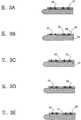
본 발명은 최소 하나의 칩으로 구성된 칩 스택을 결합시키는 사상에 기초하는데, 여기서 상기 칩은 더 이상 캐리어 바로 위에 위치하는 것이 아니라, 먼저 캐리어에 특히 절연성 또는 유전성 및/또는 광-구조화가능한(photostructurable) 기저 층을 도포하고 그 위에 순서대로 칩 스택을 형성시킨다. 유리하게는 적어도 부분적으로 상기 기저 층이, 생성될 칩 스택 또는 하이브리드 웨이퍼의 구성성분이 되는 것이 본 발명에서 청구된 바와 같이 특히 고려될 만하다. 특히, 고가의 임시 접착제가 적어도 대부분 생략될 수 있다.The invention is based on the idea of combining a chip stack consisting of at least one chip wherein the chip is no longer located directly on top of the carrier, The base layer is applied and a chip stack is formed thereon in sequence. Advantageously, at least in part, the base layer is a constituent of the chip stack or hybrid wafer to be produced, as is claimed in the present invention. In particular, at least most of the expensive temporary adhesive may be omitted.
본 발명에서 청구된 바와 같이, 적어도 상당히 서포트 구역에 대하여 감소된 부착력으로 기저 층이 캐리어에 도포되며, 상기 서포트 구역은 생성될 하이브리드 웨이퍼의 영역의 대부분 또는 캐리어 영역의 큰 부분을 포함한다. 생성될 하이브리드 웨이퍼 또는 생성될 칩 스택의 최외각 가장자리의 단지 하나의 상기 하이브리드 웨이퍼 또는 상기 칩 스택에 캐리어에 대한 큰 접착력을 갖는 접착 구역이 존재한다는 것이 본 발명에서 청구되는 바에 따라 고려된다. 환언하면: 캐리어가 칩의 최소 하나의 층의 칩 스택 및 기저 층을 홀딩하며, 상기 스택은 상기 기저 층의 주변부 상에서 다소 독점적으로, 상기 기저 층 상에 형성될 것이며, 접촉 표면은 상기 기저 층과 상기 캐리어 사이에서 평탄하다.As claimed in the present invention, the base layer is applied to the carrier with a reduced adhesion to the support zone at least substantially, the support zone comprising a majority of the area of the hybrid wafer to be produced or a large portion of the carrier area. It is contemplated by the present invention that there is only one hybrid wafer on the outermost edge of the hybrid wafer to be produced, or the chip stack to be produced, or an adhesion zone with a high adhesion to the carrier in the chip stack. In other words: the carrier will hold the chip stack and the base layer of at least one layer of the chip, the stack will be formed on the base layer rather exclusively on the periphery of the base layer, And is flat between the carriers.
본 발명에서 청구되는 바와 같이 영역 당 기저 층에 대한 접착 구역의 접착력은 특히 서포트 구역의 접착력에 비하여 최소 3배, 바람직하게는 최소 5배, 심지어 더욱 바람직하게는 최소 10배, 이상적으로는 최소 20배 더 크다.The adhesion of the adhesive zone to the base layer per zone as claimed in the present invention is at least 3 times, preferably at least 5 times, even more preferably at least 10 times, and ideally at least 20 times It is bigger.
본 발명의 목적을 위하여 캐리어는 하이브리드 웨이퍼 또는 피스 칩 스택을 제조하기에 적합한 모든 물질일 수 있으며, 특히 바람직한 물질은 금속, 세라믹 또는 반도체, 뿐만 아니라 석영, 유리 등의 그룹으로부터 선택되는 것들이다. 이들 물질의 조합으로 구성된 캐리어를 생성하는 것 또한 고려된다. 캐리어는 어떠한 형상도 가질 수 있으나, 유리하게는 정사각형, 직사각형, 또는 특히 둥근형 일 수 있다. 둥근 형상의 캐리어의 한 구체 예에서 표준 실리콘 웨이퍼와 유사하거나 동일한 치수를 갖는 기판이 특히 유리한데, 왜냐하면 이러한 경우 달성된 활용 가능한 생산 기계 및 인프라구조가 사용될 수 있기 때문이다.For the purposes of the present invention, the carrier may be any material suitable for producing a hybrid wafer or piece-chip stack, and particularly preferred materials are those selected from the group of metals, ceramics or semiconductors, as well as quartz, glass, It is also contemplated to produce a carrier comprised of a combination of these materials. The carrier may have any shape, but may advantageously be square, rectangular, or especially round. In one embodiment of the rounded carrier, a substrate having similar or identical dimensions to a standard silicon wafer is particularly advantageous since the available production machines and infrastructure achieved in this case can be used.
본 발명의 핵심은 따라서 기저 층을 캐리어에 도포하는 것으로 구성되는데, 여기서 상기 캐리어는 칩 스택의 포팅을 위하여 사용된 물질에 비하여, 화학적 관점 및 열적 관점 그리고 열기계적 관점에서, 특히 기저 층의 가장자리에서의 고정에 의해 크게 단순화된 기저 층으로부터의 캐리어의 분리와 관련하여, 우수한 특성을 가진다. 유연성 및 또한 획득 가능한 정렬 정확도 두 가지 모두가 층 물질(몰딩 화합물)에 의해 포팅되지 않은 기저 층의 결과로서 크게 개선되었다. 더욱이, 생산 비용이 특히 임시 접착제와 관련하여 고가의 물질 조합을 생략함으로써 개선된다. 최종적으로, 그리고 마지막으로, 단지 본 발명이 수 개의 칩 층을 가공하여, 칩/칩 스택, 특히 팬-아웃 결합 구조물을 전기적으로 연결시키는 도체 경로가 있는 칩 스택으로 만들 수 있다.The core of the present invention thus consists in applying a base layer to a carrier wherein the carrier is chemically and thermally and thermally mechanically inferior to the material used for porting of the chip stack, With respect to the separation of the carrier from the base layer which is greatly simplified by the fixing of the base layer. Both flexibility and also obtainable alignment accuracy have been greatly improved as a result of the underlying layer not being ported by the layer material (molding compound). Moreover, the production costs are improved by omitting expensive combinations of materials, especially with regard to temporary adhesives. Finally, and finally, the present invention can be made into a chip stack with a conductor path that processes several chip layers to electrically connect the chip / chip stack, especially the fan-out coupling structure.
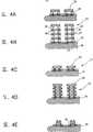
본 발명에서 청구된 또 다른 독립적인 구성에서, 기저층이 스탬핑 공정(stamping process), 예를 들어 핫 스탬핑(hot stamping) 또는 UV 스탬핑 방법(자외선에 의한 조사에 의해 가교될 수 있는 물질에 기초함)에 의해 구성될 수 있으며, 특히 최소 하나의 플라스틱 칩으로부터 형성되는 칩 스택을 생성하기 위한 플라스틱으로 구성된다는 점이 제공된다. 이러한 경우 실리콘이 본 발명에서 청구된 바와 같이 완전하게 배제될 수 있음이 고려될 수 있다. 이러한 구체 예가 미세유체(microfluidics)에서의 적용에 특히 유리할 수 있으며, 이에 따라 미세유체 칩의 생성은 본 발명에서 청구된 방법의 다양성을 나타낸다. 따라서 기저 층이 예컨대 핫 스탬핑 또는 UV 스탬핑 방법과 같은 스탬핑 방법에 의해 구성되며 그리고 선택적으로 구조물의 금속 코팅 및/또는 캡슐화가 후속하는 결합 방법에 의해 일어난다는 점에서, 칩 스택 형성 방법의 단계는 이러한 유형의 가장 일반적인 실행으로 구성된다.In another independent construction claimed in the present invention, the base layer is formed by a stamping process, such as hot stamping or UV stamping methods (based on materials that can be crosslinked by irradiation with ultraviolet light) , And in particular consists of plastic for producing a chip stack formed from at least one plastic chip. It can be considered that silicon in this case can be completely excluded as claimed in the present invention. These embodiments may be particularly advantageous for applications in microfluidics, and thus the creation of microfluidic chips represents a variety of the methods claimed in the present invention. Thus, the steps of the chip stack forming method are not limited to these steps, in that the base layer is constituted by a stamping method such as, for example, a hot stamping or UV stamping method and optionally the metal coating and / or encapsulation of the structure takes place by a subsequent bonding method. It consists of the most common types of execution.
이러한 스탬핑 방법은 또한 특히 몰딩 화합물(소위 관통 몰드 비아(through mold via) 또는 약어로서 TMV로 불림)을 통하여 연장되는 전기적 연결부의 경제적인 생성을 위하여 사용될 수 있다. 여기서 칩의 포팅은 포팅 기구가 예를 들면 몰딩 화합물에 관통 몰드 비아를 생성하기 위하여 원하는 구조를 갖는 방식으로 수행된다. 포팅 공정 동안 포팅 기구는 액체 몰딩 화합물 덩어리(mass)로 압착되고 상기 기구 내로 성형된 음각 구조물(negative structure)이 의도된 부위에서 상기 몰딩 화합물을 대체한다. 몰딩 화합물 물질의 경화 이후, 원하는 양각 구조물(positive structure)이 경화된 상기 몰딩 화합물 물질에 잔존한다. 이러한 방식으로 예를 들어 관통 몰드 비아가 생성될 수 있으며 이는 생산 공정 흐름에서 소정의 시간 경과 후에 산업분야의 종래 방법, 특히 예를 들어 금속의 전기화학적 증착을 사용하여 충전될 수 있다. 이는 특히 예를 들어 이러한 방식으로 생성된 두 개의 칩 스택이 순서대로 적층되고 서로 전기적으로 연결되는 응용분야에서 유용할 수 있다. 방금 전술한 방식으로 생성된 TMV 접촉은 두 개의 칩 스택의 단순하고 공간-절약적인 전기적 전도성 연결을 가능하게 한다.Such a stamping method can also be used for economical production of electrical connections, particularly extending through molding compounds (so-called through mold via or TMV as abbreviation). Where the porting of the chip is carried out in such a way that the potting mechanism has a desired structure, for example to create a through mold vias in the molding compound. During the potting process, the potting mechanism is squeezed into a liquid molding compound mass and a negative structure molded into the device replaces the molding compound at the intended site. After curing of the molding compound material, a desired positive structure remains in the cured molding compound material. In this way, for example, through-mold vias can be created, which can be charged after a certain period of time in the production process flow, using conventional methods in the industry, in particular electrochemical deposition of, for example, metals. This may be particularly useful in applications where, for example, two chip stacks produced in this manner are stacked in sequence and electrically connected to one another. TMV contacts created just in the manner described above enable simple, space-saving, electrically conductive connections of two chip stacks.
본 발명의 유리한 구체 예에 따르면, 접착 구역 내 캐리어 측면(carrier side) 상에, 특히 상기 캐리어 측면에 대하여 세트백(set back) 된 오프셋(offset) 상에, 바람직하게는 상기 캐리어 측면에 대하여 동일 높이 표면으로 채우는 선택적으로 가용성인 충전 물질이 존재한다는 점이 제공된다. 이러한 양상은 상응하는 용매에 의해 선택적으로 용해된 충전 물질에 의해 특히 세심한 방식으로 하이브리드 웨이퍼 또는 칩 스택으로부터의 캐리어의 분리를 가능하게 하며, 여기서 상기 용매는 다른 물질에 대하여 비선택적(nonselective)이거나 또는 적어도 대부분 구획으로 나누어질 수 있다.According to an advantageous embodiment of the invention, on the carrier side in the bonding zone, in particular on an offset set back against the carrier side, preferably the same for the carrier side There is provided a selectively soluble fill material that fills the height surface. This aspect enables the separation of the carrier from the hybrid wafer or chip stack in a particularly sensitive manner by the filler material selectively dissolved by the corresponding solvent, wherein the solvent is nonselective for the other material or It can be divided into at least most of the sections.
기재된 캐리어는 본 방법을 실시하기 위한 독립된 발명으로 간주될 수 있다.The carriers described can be considered as independent inventions for practicing the method.
전체 표면의 적어도 부분적으로 접착 구역 및 서포트 구역에 도포되는 기저 층에 의해, 캐리어 상에서 활용 가능한 영역이 칩 스택 생성을 위하여 대부분 완전하게 사용될 수 있다. 300 mm의 캐리어 지름에 대하여, 접착 구역의 가장자리로부터 서포트 구역의 가장자리까지의 거리, 특히 링의 폭(ring width)은 0.5 mm 내지 10 mm, 특히 1 mm 내지 5 mm, 바람직하게는 2 mm 내지 4 mm이다.By virtue of the base layer being applied at least partially to the adhesion zone and the support zone of the entire surface, the area available on the carrier can be largely completely used for chip stack creation. For a carrier diameter of 300 mm, the distance from the edge of the adhesive zone to the edge of the support zone, in particular the ring width, is 0.5 mm to 10 mm, in particular 1 mm to 5 mm, preferably 2 mm to 4 mm mm.
본 발명의 또 다른 유리한 구체 예에 따르면, 칩 스택은 특히 절단(cutting)에 의해, 캐리어의 분리 이전에 분리되며, 이에 따라 칩 스택은 단지 캐리어에 연결되어 있다. 이러한 경우, 동시에 기저 층이 절단되어 베이스부(base part)가 되며 이는 칩 스택에 할당된다는 점이 제공된다.According to another advantageous embodiment of the invention, the chip stack is separated, in particular by cutting, prior to the separation of the carrier, whereby the chip stack is only connected to the carrier. In this case, it is provided that at the same time the base layer is cut to become the base part, which is assigned to the chip stack.
특히 층 물질(몰딩 화합물)에 의해 포팅되는 대신, 기저 층을 형성하는 물질이 포팅을 위하여 사용되는 것과 관련하여, 기저 층을 형성하는 물질이 유연성(flexible)인 한 구체 예가 특히 유리하다. 이는 한편으로는 매우 큰 기계적 내구성을 가지며 다른 한편으로는 기계적으로 유연성인 특히 얇고 소형의 패키지를 생성하는 것을 가능하게 한다. 이는 유연성(flexibility)이 중요한 응용분야, 특히 스마트 카드 또는 굽은 표면에 대한 패키지의 추후 부착과 같은 특정한 응용분야에 대하여 특히 유리하다.Particularly in connection with the material used to form the base layer, rather than being ported by a layer material (molding compound), particular embodiments are particularly advantageous as long as the material forming the base layer is flexible. This makes it possible to create a particularly thin and compact package which on the one hand has a very high mechanical durability and on the other hand is mechanically flexible. This is particularly advantageous for certain applications, such as flexibility in applications where packaging is important, especially for later attachment of packages to smart cards or curved surfaces.
본 발명의 한 가지 특히 유리한 구체 예에 따르면, 특히 칩 스택을 형성하기 이전에, 팬-아웃 결합 구조물이 기저 층 내에서 형성되는 것이 제공된다. 이러한 방식에서, 기저 층은 또 다른 목적을 위하여 사용되며 따라서 칩 스택 또는 하이브리드 웨이퍼의 또 다른 기능성 부품을 형성한다. 이러한 경우 이러한 팬-아웃 결합 구조물을 칩의 배치 이전에 품질 테스트하여 이러한 구조물 내 가능한 결함이 비기능성 팬-아웃 결합 구조물에 적용되는 칩 또는 칩 스택에 야기되는 것을 방지하도록 하는 가능성이 특히 유리하다.According to one particularly advantageous embodiment of the invention, it is provided that the fan-out coupling structure is formed in the base layer, in particular before forming the chip stack. In this manner, the base layer is used for another purpose and thus forms another functional part of the chip stack or hybrid wafer. In such a case, it is particularly advantageous to test such a fan-out bonding structure prior to placement of the chip to prevent possible defects in such a structure from being caused in a chip or chip stack applied to the non-functional fan-out bonding structure.
팬-아웃 결합 구조물은 칩의 칩 접촉 표면에 비하여 활용 가능한 팬-아웃 접촉 표면을 확장시키는데, 이는 최소 1.5배, 바람직하게는 2배, 더욱 바람직하게는 3배, 이상적으로는 4배에 해당한다.The fan-out engagement structure expands the available fan-out contact surface compared to the chip contact surface of the chip, which is at least 1.5 times, preferably twice, more preferably 3 times, and ideally 4 times .
캐리어 측면으로부터 먼 쪽의 칩 측면(chip side) 상에 칩 스택을 형성하기 이전에, 칩 스택과 팬-아웃 결합 구조물의 전기적 결합을 위하여 접촉 패드가 도포되는 것이 특히 유리하다.It is particularly advantageous that the contact pads are applied for electrical coupling of the chip stack and the fan-out coupling structure prior to forming the chip stack on the chip side remote from the carrier side.
더욱이, 칩 스택의 형성 이전 또는 형성 동안에, 특히 결합 구조물의 도입과 동시에, 기저 층 내/상에, 특히 칩 스택의 하나의 가장자리와 동일 높이로, 기저 층 상의 접촉 패드 및/또는 칩 스택의 배치를 위한 정렬 마크를 제공하는 것이 유리하다.Moreover, it is also possible to arrange the contact pads and / or the chip stack on the base layer before / during the formation of the chip stack, in particular with the introduction of the coupling structure, in / on the base layer, in particular at the same height as one edge of the chip stack It is advantageous to provide an alignment mark for < / RTI >
그 대신에 이러한 정렬 마크는 개별 칩 상에 위치한 정렬 마크에 대응할 수 있다. 이러한 방식에서 기저 층은 또 다른, 추가 기능을 수행하며 기재된 양상에 의해 칩/칩 스택의 정렬 정확도가 더욱 증가된다. 기저 층이 광-구조화가능한 물질, 특히 광-구조화가능한 유전체(dielectric)인 경우 특히 유리하다.Instead, such an alignment mark may correspond to an alignment mark located on an individual chip. In this manner, the base layer performs yet another, additional function, and the alignment accuracy of the chip / chip stack is further increased by the aspects described. It is particularly advantageous when the base layer is a photo-structurable material, in particular a photo-structurable dielectric.
대안적인 독립적 구체 예에 따르면, 칩 스택이 결합(접착)에 의해 기저 층에 직접 결합되는 점이 제공된다. 이는 추가적인 접착제의 도움으로 또는 기저 층 물질의 가능한 접착 특성을 사용하여 수행될 수 있다. 따라서 칩이 소위 다이 부착 접착제(die attach adhesive)에 의해 접합(cemented)되는 것이 본 발명에서 청구된 바에 따라 고려될 수 있다. 그 대신에 기저 층 물질이 유전체이며 이는 노출안된 상태에서 대부분 열가소성 거동을 갖는다는 점이 본 발명에서 청구된 바와 같이 고려될 수 있다. 따라서 칩은 열가소성 접착 공정에 의해 고정될 수 있다.According to an alternative independent embodiment, it is provided that the chip stack is directly bonded to the base layer by bonding (adhesion). This can be done with the aid of additional adhesive or using possible adhesive properties of the base layer material. Thus, it is contemplated that the chip may be cemented by a so-called die attach adhesive, as claimed in the present invention. Instead, it can be considered as claimed in the present invention that the base layer material is a dielectric and has mostly thermoplastic behavior in the unexposed state. Thus, the chip can be fixed by a thermoplastic bonding process.
칩 스택을 형성한 이후 그리고 캐리어를 분리하기 이전에, 칩 스택을 특히 기저 층에 상응하는 층 물질로 포팅하는 것이 유리한데, 왜냐하면 이러한 방식에서 특히 유연하고 동시에 안정한 칩 스택 또는 하이브리드 웨이퍼가 형성될 수 있기 때문이다.It is advantageous to port the chip stack, especially after forming the chip stack and before separating the carrier, to a layer material corresponding to the base layer, because in this way a particularly flexible and stable chip stack or hybrid wafer can be formed It is because.
본 발명의 또 다른 대안적인 구체 예에 따르면, 특히 접착 층의 접착력을 감소시켜 캐리어의 한쪽 측면 가장자리로부터 캐리어를 분리시키는 것이 바람직하게는 충전재 물질의 선택적 용해에 의해 수행된다는 것이 제공된다. 특히 포팅 물질을 위하여, 기저층에 도포된 칩 스택 및 기저층으로부터 캐리어를 분리시키는 것은 본 발명에 기재된 이러한 방식에 의해 조심스럽게 수행된다.According to another alternative embodiment of the present invention, it is provided that the separation of the carrier from one side edge of the carrier, in particular by reducing the adhesive strength of the adhesive layer, is preferably carried out by selective dissolution of the filler material. Particularly for the potting material, the separation of the carrier from the chip stack and base layer applied to the base layer is carefully carried out in this manner as described in the present invention.
캐리어는 특히 접착 구역에서 작용하는 연결 해방 수단(connection release means)에 의해, 그리고 기저 층과 캐리어 사이의 접착 구역에서 작용하는 접착 수단에 의해, 본 발명에 기재된 바에 따라 기저 층으로부터 분리된다.The carrier is separated from the base layer according to the description of the invention, in particular by connection release means acting in the adhesion zone and by means of adhesion acting in the adhesion zone between the base layer and the carrier.
연결 해방 수단은 유동화제일 수 있으며, 특히 연결부를 선택적으로 용해시키는 용매일 수 있다. 화학적 용해는 특히 조심스러우며 상응하는 물질 선택에 의해, 특히 캐리어 또는 기저 층의 단지 가장자리 구역에 접착 층이 제공되어 용매가 측면으로부터 신속하게 작용할 수 있을 때, 용해가 신속하게 일어날 수 있다.The connection releasing means can be a fluidizing agent, and in particular, can be used for selectively dissolving the connecting portion. Chemical dissolution is particularly careful and dissolution can occur rapidly, with corresponding material choices, especially when the adhesive layer is provided on only the edge region of the carrier or base layer so that the solvent can act quickly from the side.
본 발명의 하나의 대안적인 구체 예에 따르면, 연결 해방 수단이, 접착제를 용해시키기 위해, 기계적 분리 수단, 특히 접착 구역에서 캐리어로부터의 기저 층의 기계적 분리를 위한 블레이드(blade)를 포함한다는 점이 제공된다. 기계적 분리 수단과 유동화제의 조합이 또한 고려될 수 있다. According to one alternative embodiment of the invention, it is provided that the connection releasing means comprises a mechanical separating means, in particular a blade for mechanical separation of the base layer from the carrier in the adhesive zone, for dissolving the adhesive do. The combination of the mechanical separating means and the fluidizing agent can also be considered.
본 발명의 또 다른 대안적인 구체 예에 따르면, 연결 해방 수단이 기저 층과 캐리어 사이의 접착제를 용해시키기 위한 UV 광원을 포함한다는 점에 제공된다. 이러한 구체 예는 또한 기계적 분리 수단의 구체 예 및/또는 유동화제의 구체 예와 조합될 수 있다.According to another alternative embodiment of the present invention, it is provided that the connection releasing means comprises a UV light source for dissolving the adhesive between the base layer and the carrier. These embodiments may also be combined with embodiments of mechanical separation means and / or embodiments of fluidizing agents.
연결 해방 수단이 캐리어의 하나의 측면 가장자리로부터 특히 배타적으로 작용하도록 구성되는 정도에서, 특히 캐리어의 측면 가장자리 또는 서포트 구역 내에 위치하는 캐리어의 영역의 상단 및/또는 하단으로부터 캐리어 및/또는 하이브리드 웨이퍼/칩 스택에 대한 작용이 종종 생략될 수 있다.The carrier and / or hybrid wafer / chip from the top and / or bottom of the area of the carrier located in the lateral edge of the carrier or in the support zone, to the extent that the connection and release means are configured to act exclusively one side edge of the carrier, The action on the stack can often be omitted.
캐리어의 전체 주변부 상부의 연결 해방 수단의 배열이 생략될 수 있고 캐리어의 주변부에 대한 부분적인 작용이 캐리어의 회전을 위한 회전 수단으로서 충분하다.The arrangement of the connection releasing means on the entire peripheral portion of the carrier can be omitted and the partial action on the peripheral portion of the carrier is sufficient as the rotating means for rotation of the carrier.
유리하게는, 접착 층을 유동화제에 노출시키기 위해, 유동화제를 홀딩하기 위한 용매 탱크가 존재하며 이는 특히 밀봉되며 캐리어 또는 캐리어 수령부에 접촉한다. 캐리어의 측면 가장자리 또는 주변부를 적어도 부분적으로 에워싸는 용매 탱크에 의해, 연결 층에 대한 특히 효과적인 작용이 가능하다. 더욱이 밀봉 방안은 유동화제가 용매 탱크로부터 방출되는 것을 방지하거나 또는 UV 광 세기가 상실되는 것을 방지한다. 기계적 분리 수단이 사용될 때, 가능한 불순물이 용매 탱크로부터 방출되거나 또는 하이브리드 웨이퍼 또는 칩 스택을 오염시키는 것이 방지된다. 유리한 구성에서 용매 탱크는 L-형 또는 U-형 횡단면으로 형성될 수 있다.Advantageously, in order to expose the adhesive layer to the fluidizing agent, there is a solvent tank for holding the fluidizing agent, which is particularly sealed and contacts the carrier or carrier receiver. A particularly effective action on the connection layer is possible by means of a solvent tank at least partly surrounding the side edge or periphery of the carrier. Moreover, the sealing measures prevent the fluidizing agent from being released from the solvent tank or prevent the UV light intensity from being lost. When a mechanical separation means is used, it is prevented that possible impurities are released from the solvent tank or contaminate the hybrid wafer or chip stack. In an advantageous configuration, the solvent tank may be formed as an L-shaped or U-shaped cross-section.
접착 층, 특히 선택적 가용성(soluble) 충전재 물질의 용해는 조절기에 의해 본 발명에서 청구된 바에 따라 가속될 수 있는데, 상기 조절기(modulator)는 초음파(ultrasonically) 또는 메가음파(megasonically)에 의해 발생된 캐비테이션(cavitation)에 의해 캐리어의 분리를 크게 가속시키며 이에 따라 분리는 훨씬 더욱 조심스럽게 그리고 동시에 더욱 신속하게 일어난다. 조절기는 최적의 음파 전달(sonic transmission)을 위하여 사용된 용매와 접촉한다. 유리하게는 조절기는 L-형 또는 U-형 용매 탱크에 기계적으로 일체화된다. 그 대신에 조절기는 용매가 접착 층을 분리시키기 위해 의도된 방식으로 공급되는 즉시 용매에 침적될 수 있다.The dissolution of the adhesive layer, in particular the soluble filler material, can be accelerated by a regulator as claimed in the present invention, wherein the modulator is cavitation generated by ultrasonics or megasonically which greatly accelerates the separation of the carrier by cavitation and thus the separation takes place much more carefully and at the same time more rapidly. The regulator contacts the solvent used for optimal sonic transmission. Advantageously, the regulator is mechanically integrated into the L-type or U-type solvent tank. Instead, the regulator can be immersed in the solvent as soon as the solvent is fed in the intended manner for separating the adhesive layer.
본 발명은 또한 캐리어에 관한 것이며 캐리어 측면에는 접착 작용성인 접착 구역 및 상기 접착 구역보다 접착성이 작은 서포트 구역이 제공되며, 기저 층 (20)이 적어도 서포트 구역에 대한 전체 표면에 대부분 적용가능하며, 접착 구역 내 캐리어 측면 상에는, 특히 캐리어 측면에 대하여 세트백 된 오프셋 상에는, 상기 캐리어 측면과 동일한 표면 높이로, 선택적으로 가용성인 충전재 물질이 존재한다. 이러한 방식으로 장착된 캐리어에 의해, 본 발명에 청구된 방법은 특히 유리한 방식으로 수행될 수 있는데 왜냐하면 캐리어로부터의 하이브리드 웨이퍼 또는 칩 스택의 분리(detachment)가 적어도 주로 칩 스택 및 몰딩 화합물에 불리한 영향을 주지 않으면서 일어나기 때문이다. 이러한 방식으로 특히 고가의 칩 스택의 조심스러운 분리가 보장된다. 더욱이, 칩 스택이 형성되거나 및/또는 팬-아웃 결합 구조물이 칩 스택 구조물에 형성될 때 수 개의 이웃하는 칩 스택을 상호 연결시키는 것이 본 발명에서 청구되는 바에 따라 고려된다(구체 예 F 참조).The present invention also relates to a carrier, wherein the carrier side is provided with a bonding zone which is adhesive and a support zone which is less adhesive than said bonding zone, the base layer (20) being at least applicable to the entire surface for at least the support zone, On the carrier side, particularly on the carrier side in the adhesion zone, there is a selectively soluble filler material at the same surface height as the carrier side, on the offset set back against the carrier side. With the carrier mounted in this way, the method claimed in the present invention can be carried out in a particularly advantageous manner, since the detachment of the hybrid wafer or chip stack from the carrier will at least mainly have a detrimental effect on the chip stack and the molding compound Because I wake up without giving. In this way a careful separation of the particularly expensive chip stack is ensured. Furthermore, interconnecting several neighboring chip stacks when the chip stack is formed and / or the fan-out coupling structure is formed in the chip stack structure is considered as claimed in the present invention (see embodiment F).
캐리어의 분리가 캐리어의 주변부로부터 동심원적으로 캐리어의 중심부로 일어나는 것이 또한 유리하게 제공된다.It is also advantageously provided that the separation of the carrier occurs concentrically from the periphery of the carrier to the center of the carrier.
본 발명의 또 다른 장점, 특징, 및 상세사항은 이하의 바람직한 예시적인 구체 예의 설명 및 도면을 사용하여 명백하게 될 것이다.
도 1A 내지 1E, 9F1, 10G1 및 11H1는 구체 예 A 내지 H에 의해 본 발명에서 청구된 바에 따라, 기저 층을 캐리어에 적용하는 단계의 개략도를 나타낸다.
도 2A 내지 2E 및 11H2는 구체 예 A 내지 E 및 H에 의해 본 발명에서 청구된 바에 따라, 기저 층으로 팬-아웃 결합 구조물 및 정렬 마크를 도입시키는 단계의 개략도를 나타낸다.
도 3A 내지 3E 및 11H3은 구체 예 A 내지 E 및 H에 의해 본 발명에서 청구된 바에 따라, 접촉 패드를 기저 층 상에 위치시키는 단계의 개략도를 나타낸다.
도 4A 내지 4E, 9F2, 10G4 및 11H4는 구체 예 A 내지 H에 의해 본 발명에서 청구된 바에 따라, 칩을 기저 층 상에 적어도 한 위치에서 적층시키는 단계의 개략도를 나타낸다.
도 5A 내지 5E, 10G5 및 11H5는 구체 예 A 내지 E, G 및 H에 의해 본 발명에서 청구된 바에 따라, 칩 스택을 몰딩 화합물로 포팅시키는 단계의 개략도를 나타낸다.
도 6A 내지 6E, 9F6, 10G6 및 11H7은 구체 예 A 내지 H에 의해 본 발명에서 청구된 바에 따라, 칩 스택이 있는 기저 층을 캐리어로부터 분리시키는 단계의 개략도를 나타낸다.
도 7A 내지 7E, 10G10 및 11H8은 구체 예 A 내지 E, G 및 H에 의해 본 발명에서 청구된 바에 따라, 솔더링된(soldered) 연결부(범프)를 적용하는 단계의 개략도를 나타낸다.
도 8A 내지 8E, 9F7, 10G11 및 11H9는 구체 예 A 내지 H에 의해 본 발명에서 청구된 바에 따라, 캐리어 상의 칩 스택 또는 하이브리드 웨이퍼를 분리시키는 단계의 개략도를 나타낸다.
도 9F3은 구체 예 F에 의해 본 발명에서 청구된 바에 따라, 기저 층에 상응하는 층 물질로 포팅하는 단계의 개략도를 나타낸다.
도 9F4는 구체 예 F에 의해 본 발명에서 청구된 바에 따라, 팬-아웃 결합 구조물을 도입하는 단계의 개략도를 나타낸다.
도 9F5는 구체 예 F에 의해 본 발명에서 청구된 바에 따라, 추후 또 다른 칩 및 솔더링된 연결부(범프)를 적용하는 단계의 개략도를 나타낸다.
도 10G2는 구체 예 G에 의해 본 발명에서 청구된 바에 따라, 리소그라피 단계의 개략도를 나타낸다.
도 10G3은 구체 예 G에 의해 본 발명에서 청구된 바에 따라, 리소그라피 단계의 개략도를 나타낸다.
도 10G7은 구체 예 G에 의해 본 발명에서 청구된 바에 따라, 하이브리드 웨이퍼를 180o 회전시키는 단계의 개략도를 나타낸다.
도 10G8은 구체 예 G에 의해 본 발명에서 청구된 바에 따라, 에칭 단계의 개략도를 나타낸다.
도 10G9는 구체 예 G에 의해 본 발명에서 청구된 바에 따라, 팬-아웃 결합 구조물을 도입하는 단계의 개략도를 나타낸다.
도 11H6은 구체 예 H에 의해 본 발명에서 청구된 바에 따라, 충전재 물질을 용해시키는 단계의 개략도를 나타낸다.
도면은 구체 예 A 내지 H의 개별 단계 또는 복수의 단계를 나타내며, 도면의 부호는 참조 부호 A 내지 H에 의해 식별된다. 구체 예 A 내지 E의 개별 단계는 각각 한쪽 측면(side) 상에서 함께 제시되며, 한편 구체 예 F, G, 및 H의 단계는 순차적으로 제시된다.
이러한 묘사는 캐리어를 조작하기 위한 및/또는 개별 단계를 수행하기 위한 종래 공지된 장치 없이 제시된다.
참조 번호는 비록 서로 다른 구체 예에 대하여 서로 다른 방안/물질이 선택되더라도 상응하는 부분에 대하여 동일하게 사용된다.Further advantages, features and details of the present invention will become apparent from the following description of preferred exemplary embodiments and the drawings.
Figures 1A-1E, 9F1, 10G1, and 11H1 show schematic views of applying a base layer to a carrier, as claimed in the present invention by embodiments AH.
Figures 2A through 2E and 11H2 show schematic views of the step of introducing the fan-out bonding structure and the alignment mark into the base layer, as claimed in the present invention by embodiments A through E and H.
Figures 3A-3E and 11H3 show a schematic diagram of the step of placing a contact pad on the base layer, as claimed in the present invention by embodiments A through E and H.
Figures 4A through 4E, 9F2, 10G4, and 11H4 illustrate schematic views of depositing chips on at least one location on the base layer, as claimed in the present invention by embodiments A through H.
Figures 5A through 5E, 10G5 and 11H5 show schematics of the step of porting the chip stack to the molding compound, as claimed in the present invention by embodiments A through E, G and H.
Figures 6A through 6E, 9F6, 10G6, and 11H7 illustrate a schematic diagram of the step of separating the base layer with the chip stack from the carrier, as claimed in the present invention by embodiments A through H.
Figures 7A through 7E, 10G10 and 11H8 show schematic views of applying soldered connections (bumps), as claimed in the present invention by embodiments A through E, G,
Figures 8A to 8E, 9F7, 10G11, and 11H9 show schematic views of steps for separating a chip stack or a hybrid wafer on a carrier, as claimed in the present invention by embodiments A to H.
Figure 9F3 shows a schematic view of the step of porting to a layer material corresponding to the base layer, as claimed in the present invention by Embodiment F.
Figure 9F4 shows a schematic diagram of the step of introducing a fan-out coupling structure, as claimed in the present invention by embodiment F.
9F5 shows a schematic view of the step of applying another chip and soldered connections (bumps), as claimed in the present invention by embodiment F. Fig.
FIG. 10G2 shows a schematic view of the lithography step, as claimed in the present invention by embodiment G. FIG.
FIG. 10G3 shows a schematic view of the lithography step, as claimed in the present invention by embodiment G. FIG.
10G7 is also, as claimed in the invention by the embodiments G, it shows a schematic view of the step of rotating the hybrid wafer 180o.
FIG. 10G8 shows a schematic view of an etching step, as claimed in the present invention by embodiment G. FIG.
FIG. 10G9 shows a schematic diagram of the step of introducing a fan-out coupling structure, as claimed in the present invention by embodiment G. FIG.
Figure 11H6 shows a schematic view of a step of dissolving the filler material, as claimed in the present invention by embodiment H.
The figures represent individual steps or steps of embodiments A through H, where the reference numerals are identified by reference numerals A through H. The individual steps of embodiments A through E are each presented together on one side, while the steps of embodiments F, G, and H are presented sequentially.
This description is presented without the prior art devices for manipulating the carrier and / or performing the individual steps.
Reference numerals are used identically for the corresponding parts, even if different measures / materials are selected for different embodiments.
본 발명의 핵심 주제는 칩(30) 또는 칩 스택(31)을 고정하기 위한 임시 접착제가 완전하게 또는 적어도 대부분 배제된다는 것이다. 그 대신에, 하이브리드 웨이퍼(34)와 캐리어(10) 사이의 접촉 표면(18) 상에 감소된 접착력을 갖는 서포트 구역(11)을 포함하는 캐리어(10) 가 사용된다. 감소된 접착력을 갖는 이러한 서포트 구역(11)은 생성될 하이브리드 웨이퍼(34) 의 영역의 대부분과 결합하며 상기 하이브리드 웨이퍼(34)는 순서대로 한 번에 최소 하나의 칩 층(33)을 갖는 복수의 칩 스택(31)으로 구성된다. 시스템은 생성될 하이브리드 웨이퍼(34)의 최외각 가장자리(35) 상에 위치한 특히 환형의 부품 표면(18)만이, 큰 홀딩 힘/접착력으로 접착 구역(14) 상의 캐리어(10) 상의 접촉 표면(18) 상에 놓이게 되도록 구성된다.A key theme of the present invention is that the temporary adhesive for fixing the
본 발명의 목적을 위하여, 캐리어(10)는 하이브리드 웨이퍼(34)를 생성하기에 적합한 어떠한 물질일 수도 있다. 그러나 전형적으로 물질은 금속, 세라믹, 또는 반도체뿐만 아니라 석영, 유리 등의 그룹 중 어느 하나로부터 선택되는 것이다. 적절한 구체 예에서 캐리어(10)는 원형 형상을 가지며 300 mm 지름의 표준 웨이퍼로서 제조된다.For purposes of the present invention, the
캐리어(10)의 서포트 구역(11)은 충전 층(19)에 의해 형성되는데(도 1A 참조) 상기 충전 층(19)은 캐리어 측면(15)에 대하여 동일 높이 표면으로 캐리어에 위치한다. 충전 층(19)의 두께는 최소 3 ㎛ 내지 100 ㎛, 바람직하게는 10 ㎛ 내지 50 ㎛이다.The
충전 층(19)의 도포/공급은 예를 들어 스핀 코팅에 의해 수행된다. 충전 층(19)은 특히 5 내지 50중량% 고체, 특히 15 내지 30중량% 고체를 갖는 물질로 구성되며, 상기 고체는 모노머, 올리고머 및/또는 폴리머, 바람직하게는 사이클릭 올레핀 폴리머 및/또는 코폴리머 및/또는 높은 원자 불소 함량, 특히 30중량% 초과, 바람직하게는 45중량% 초과의 비결정질 플루오로폴리머의 그룹으로부터 선택된다.The application / supply of the
환언하면, 충전 층(19)은 이하에서 설명하는 특징 중 한 가지 이상을 가진다:In other words, the filling
-충전 층(19)은 특히 낮은 자유 표면 에너지를 갖는 비결정질 폴리머 물질로 구성된다.The filling
-충전 층(19)은 낮은 내지 매우 낮은 농도의 하이드록실 그룹 또는 카르복실산 그룹을 갖는 적어도 표면 상의 충전 층(19)에 대하여 실리콘, 유리 및/또는 금속 표면에 관한 낮은 접착성 내지 비접착성을 가진다.The filling
-충전 층(19)은 용액으로부터 제조될 수 있다.The filling
특히 수 개 층으로의 칩(30)의 적층은 해당 분야의 통상의 기술자에게 공지되어 있다. 본 발명에 기재된 구성에 있어서, 적층은, 특히 칩 가장자리(37) 상에서, 기저 층(20)의 정렬 마크(25)에 대한 칩(30)의 정렬을 위하여 사용되는 칩 정렬 마크(38)를 갖는, 각각의 칩(30)에 의해 개선된다(도 4B 참조). 서포트 구역(11)은 교대로 생성될 수 있거나 또는 이하에서 설명하는 단계에 의해 그 표면에서 가공될 수 있다:The lamination of the
-자유 표면 에너지를 감소시키기 위한, 소수성 유기실란 예를 들면 불소/알킬 포스포네이트 또는 (플루오로)알킬 실란을 사용한 실리콘으로부터 형성된 표면의 화학적 처리, 또는- chemical treatment of the surface formed from silicon with hydrophobic organosilanes such as fluorine / alkyl phosphonates or (fluoro) alkylsilanes to reduce free surface energy, or
-서포트 구역 내에 또는 서포트 구역으로서 영구적 항-접착 코팅을 형성하기 위한, 캐리어 상에 낮은 자유 표면 에너지를 갖는 코팅(예컨대 불소화 파릴렌(fluorinated parylenes))의 화학 기상 증착(CVD 법).- Chemical vapor deposition (CVD) of a coating (e.g. fluorinated parylenes) with low free surface energy on the carrier to form a permanent anti-adhesive coating in the support zone or as a support zone.
이러한 코팅의 두께는 특히 1 nm 내지 20 nm, 바람직하게는 2 nm 내지 10 nm이다.The thickness of such a coating is in particular from 1 nm to 20 nm, preferably from 2 nm to 10 nm.
캐리어(10)의 표면의 적어도 일부의 화학적 개질에 의해 생성된 이러한 서포트 구역(11)의 생성은 한 바람직한 구체 예를 따라 진행된다.The production of such a
에폭시계 포토레지스트를 실리콘 웨이퍼의 외각 주변부 상의 환형 섹션(접착 구역(14))에서 300 mm 지름의 실리콘 웨이퍼(캐리어(10))의 표면에 도포한다. 링의 폭은 1 내지 10 mm이다. 불소화 실란을 적절한 용매로 희석하여 1% 용액을 만든다. 이러한 용액을 스핀 코팅을 사용하여 실리콘 웨이퍼의 표면에 도포한다. 그 후 웨이퍼를 100℃의 가열 플레이트 상에서 1분 동안 경화시킨다. 그 후 웨이퍼를 스핀 코터(spin coater)에서 표면 높이를 동일하게 하고 다시 100℃에서 1분 동안 경화시킨다. 그 후 에폭시계 포토레지스트를 스핀 코터 내에서 아세톤으로 제거하고, 그 결과 원형 접착 구역이 불소화 실란 용액에 의해 처리되지 않는 접착 구역으로 남는다. 서포트 구역(11)을 갖는 캐리어(10)가 완성된다.The epoxy-based photoresist is applied to the surface of a 300 mm diameter silicon wafer (carrier 10) in an annular section (adhesive zone 14) on the outer periphery of the silicon wafer. The width of the ring is 1 to 10 mm. Dilute the fluorinated silane with a suitable solvent to make a 1% solution. This solution is applied to the surface of a silicon wafer using spin coating. The wafer is then cured on a hot plate at 100 DEG C for 1 minute. The wafer is then cured in a spin coater at the same surface height and again at 100 占 폚 for 1 minute. The epoxy-based photoresist is then removed with acetone in a spin coater, with the result that the circular adhesion zone remains as an adhesion zone that is not treated by the fluorinated silane solution. The
그 후 기저 층(20)을 상기 캐리어(10)의 대부분 전체 면적 상부에 적용한다. 특히 기저 층(20)은 추후 적어도 부분적으로 하이브리드 웨이퍼의 일부분이 된다. 그렇지만 개별적 경우에 이러한 기저 층을 적어도 부분적으로 칩 스택의 형성 동안 단지 임시적으로 사용하는 것을 고려할 수 있다. 이러한 경우, 추후 적절한 위치에서 상기 층을 전체 생성 공정 과정에서 다시 대부분 완전하게 제거할 수 있다. 이러한 연결부에서, 최초 존재하는 층의 최소 99.5%, 더욱 이상적으로는 99.9% 또는 심지어 더욱 이상적으로는 99.99%가 제거되는 것이 이상적으로 완전하게 간주된다. 이러한 단지 임시로 사용된 기저 층과 관련하여, 특히 유리한 구체 예가 수행될 수 있는데, 여기서 이러한 기저 층은 추후 상기 층을 제거하여 노출될 수 있고 이에 따라 접근 가능하게 되는 전기 전도성 금속 연결부의 생성을 위해 사용된다. 이러한 공정은 반도체 산업에서 전통적이며 용어 "희생층"으로 알려져 있다. 이러한 구조물을 실행하기 위하여, 이러한 구조물의 구성에 따라, 상기 기저 층이 광-구조화가능한 물질로 구성되는 것이 유리할 수 있다. 이러한 연결부에서 이는 전체 표면 상부의 대부분에서 감소된 접착제 두께를 갖는 서포트 구역(11)의 최소 90%로서 이해될 수 있다. 그렇지만 최적의 구체 예에서 이러한 표면은 최소 98%이거나 또는 심지어 더욱 이상적으로는 서포트 구역(11)보다 더 크다. 300mm 지름의 둥근 캐리어(10)에서, 큰 접착력을 갖는 접착 구역(14)은 > 0.5 mm, 이상적으로는 > 1 mm 그리고 심지어 더욱 이상적으로는 > 2 mm 또는 > 4 mm의 링 폭(ring width)을 가진다.The
기저 층(20)이 서포트 구역(11)보다 더 넓은 영역을 덮는 경우, 구체 예 F에 따르면, 캐리어(10)가 큰 접착력의 영역에서 오프셋(12)을 갖는 것이 바람직하다. 이러한 오프셋(12)은, 기저 층(20)을 도포하기 이전에, 충전 물질(13)이 서포트 구역(11)과 동일 높이의 평탄 캐리어 측면(15)을 형성할 때까지, 충전 물질(13)로 채워진다. 충전 물질(13)은 이상적으로는 선택적으로 용해될 수 있거나 또는 외부로부터 제어된 작용에 의해 추후 제거될 수 있는 물질이다. 이러한 작용을 위한 메커니즘은 기계적, 광학적 및 화학적 방법 또는 이들 방법의 조합일 수 있다. 예를 들어, 특정 용매에 의해 용해될 수 있는 물질, 특히 플라스틱이 사용될 수 있다. 한 대안적인 구체 예에 따르면, 특정 에칭 화학제에 의해 용해될 수 있는 무기 물질이 또한 가능하다. 더욱이, 자외선 (UV) 조사 또는 적외선 (IR) 조사의 작용 하에서 용해될 수 있는 물질이 고려될 수 있다. 오프셋(12)이 여기서 형성되며 이에 따라 작은 홀딩 힘을 갖는 서포트 구역(11)은 대략적으로, 특히 정확하게, 오프셋(12)의 스텝(17)까지 연장된다. 스텝(17)은 직각 가장자리 형태 또는 비스듬히 연장되는 가장자리 형태로 형성될 수 있다. 이러한 방식에서 습식 에칭 공정에 의해 비스듬히 연장되는 가장자리를 생성하는 것이 유리하게 가능하며, 실리콘의 결정 구조 형성은 이러한 비스듬한 가장자리를 자동으로 생성한다.If the
기저 층(20)은 스핀 또는 스프레이 코팅 또는 라미네이션에 의해 도포될 수 있다. 별도의 경우 또 다른 방법이 또한 가능하며, 예컨대 닥터링(doctoring), 캐스팅(casting), 압출 코팅(extrusion coating) 등이 있다.The
본 발명의 한 바람직한 구체 예에서, 기저 층(20) 물질은 광-구조화가능한 물질, 특히 광-구조화가능한 유전체이다. 예를 들어, 벤조사이클로부텐, WPR 5100 (from JSR®), ShinEtsu Chemicals®가 시판중인 SiNR® 또는 Hitachi Chemicals사 또는 Sumitomo Bakelite사가 시판 중인 유사한 생성물, 뿐만 아니라 폴리이미드가 사용될 수 있다. 해당 분야의 통상의 기술자는 이러한 물질들을 알고 있으며 최종적인 응용분야 및 생성 공정 흐름에 의해 정의되는 조건에 따라 이들을 선택할 수 있다. 한 바람직한 구체 예에서(A, B, C, D 및 H), 칩(30)의 요구되는 배선 레벨(wiring level)을 위한 도체 경로(21)는 기저 층(20) 상에 형성되는 생성될 수 있다. 이는 일반적으로 리소그라피 및 부가 공정에 의해 일어난다. 예를 들어, 개별 도체들 사이의 절연부는 전술한 감광성(photosensitive) 유전 물질로 생성될 수 있으며 한편 금속 연결부는 장벽 씨드 증착(barrier seed deposition)(스퍼터링) 및 전기화학적 증착(전기도금)에 의해 생성될 수 있다. 이러한 공정은 산업분야에서 전통적이며 해당 분야의 통상의 기술자에게 공지되어 있다. 후속하여 추후 칩(30)을 홀딩하고 결합시키기 위해 사용되는 접촉 패드(22)를 생성한다. 이러한 접촉 패드(22)와 함께 이상적으로는 기저 층(20)에 대하여 칩(30)의 정확한 정렬을 가능하게 하는 정렬 마크(25)가 또한 존재한다. 따라서 외부 정렬 수단이 배제될 수 있으며; 이는 칩(30)의 훨씬 더욱 정확한 정렬을 유발한다.In one preferred embodiment of the present invention, the
한 대안적인 구체 예 G에서 기저 층(20)은 단순히 노출되고 노출 이후 가열 공정("노출 후 베이크")을 거치게 된다. 이러한 순서는 음성 레지스트(negative resist)의 경우에 노출된 부분이 화학적으로 가교(interlink)되도록 하며, 이에 따라 현상 용액에 대하여 불용성이 되며, 한편 노출 안된 부분은 가용성으로 남게 된다. 양성 레지스트의 경우 정확하게 상반되게 거동한다: 즉 노출된 부분이 열등하게 가용성으로 남는다. 여기서 대부분의 유전 물질이 음성 레지스트 거동을 갖는다는 점에 대하여 완전함을 위하여 주목하여야 한다. 그 후 상호연결 층이 공정 A, B, C, D 및 H와 유사하게 이미 노출된 기저 층(20) 위에 직접 형성될 수 있거나 또는 칩(30)이 기저 층(20) 위에 직접 위치한다. 이러한 경우 노출된 유전체의 가열 이전에 칩(30)을 도포하고, 그 후 칩(30)과 기저 층(20)의 유전 물질 사이의 영구적 접착 연결(결합 연결)을 획득하기 위하여 또한 가교 공정(crosslinking process)을 사용하는 것이 유리할 수 있다(구체 예 G).In one alternative embodiment G, the
또 다른 대안적인 구체 예(도 9F1 내지 9F7에 따른 공정 흐름 F)는 칩(30)이 단지 기저 층(20) 상에 접합되는 것을 요구한다. 이는 추가 접착제의 도움으로 또는 상응하는 선택된 기저 층(20) 물질의 가능한 접착 성질을 사용하여 수행될 수 있다. 칩(30)이 소위 다이 부착 접착제에 의해 접합되는 것을 본 발명의 청구된 바에 따라 고려할 수 있다. 그 대신에 기저 층(20) 물질은 유전체(dielectric)일 수 있으며, 특히 노출 안된 상태에서 대부분 열가소성 거동을 갖는 전술한 물질 중 어느 하나일 수 있다. 따라서 칩(30)은 열기계적 접착 방법에 의해 고정될 수 있다.Another alternative embodiment (process flow F according to FIGS. 9F1 through 9F7) requires that the
구체 예 A, B, C, D 및 H에 대하여, 접촉 패드(22)를 생성한 이후, 칩(30) 또는 한 번에 최소 하나의 상기 칩(30)으로부터 형성된 칩 스택(31)을 배치한다. 이는 기존의 칩-투-웨이퍼 결합 방법(chip-to-wafer bonding method)에 의해 수행되며, 전형적으로 칩(30)은 사전에 미리 임시 접착제에 의해 고정되며 단지 추후에 영구적 결합이 역흐름 공정(reflow process)에서 형성된다. 이러한 점에서 구체 예 A 및 B는 범프(36)에 대한 한 양상을 나타내는데 여기서 칩은 플럭스 또는 무-흐름 언더필(no-flow underfill)에 의해 고정된다. 단지 모든 칩(30)이 기저 층(20) 상에 위치된 이후, 사전에 고정된 복수의 칩(30)을 갖는 캐리어(10)가 열 공정을 거치게 되며("역흐름 공정") 여기서 범프(36)와 접촉 패드(22)가 서로에 대해 솔더링된다(soldered). 여기서 플럭스는 접촉 표면의 산화가 가열 동안 일어나지 않는 것을 보장한다. 그 대신에 소위 무-흐름 언더필은 동일한 기능을 하는 것으로 간주되며 추후 칩(30) 사이의 영구적인 결합 경계면 부분을 남기며 이에 따라 개선된 기계적 안정성을 제공한다. 따라서 무-흐름 언더필은 칩(30) 사이의 갭의 추후 언더필링(underfilling)을 배제한다(공정 A 및 B에 제시됨). 이러한 무-흐름 언더필 물질을 사용할 때 열 공정 동안 또한 칩에 압력을 인가하는 것이 흔히 필수적이며; 이는 캐리어 상에 위치한 모든 칩에 동시에 압력을 인가할 수 있는 압력 플레이트에 의해 유리하게 수행될 수 있다.For embodiments A, B, C, D and H, after creating the
구체 예 C, D 및 H에서 범프(36)가 배제되고 그 대신 평면 표면을 사용하는 연결부가 제시된다. 이는 추가 순서에서 더욱 치밀한 연결부를 가능하게 하는데 왜냐하면 또 다른 종래 범프(36)가 배제되기 때문이다. 이러한 특별한 형태의 연결부는 소위 "과도 액상(transient liquid phase) (TLP)" 결합 공정에 의해 통상적으로 생성된다. 여기서 공융 금속 연결부(eutectic metal connection)가 형성되는데 여기서 제1 금속이 액체상으로부터 제2 금속으로 확산하고 그 후 상기 제1 금속의 녹는점보다 높은 녹는점을 갖는 안정한 금속간 연결부(intermetallic connection)를 형성한다. 따라서, 결합 연결(bond connection)이 저온에서 수행될 수 있으며 추후 최초 결합 온도보다 높은 녹는점을 갖는다. 이는 이러한 연결부를 칩(30)의 수 개의 칩 층(33)의 적층에 특히 적합하도록 만드는데 왜냐하면, 이에 의해 이미 결합된 평면의 연결부가 더 이상 불리한 영향을 받지 않기 때문이다. 이러한 결합 연결에 대한 한 가지 전형적인 예는 구리와 주석의 연결일 수 있다. 그러나 구리와 인듐, 금과 주석, 니켈과 주석, 및 금과 인듐에 대한 또 다른 가능성이 존재할 수 있다. 따라서 예를 들어 이러한 구리-주석 결합 경계면에 대한 결합 온도는 예를 들어 270 내지 280℃이며 반면 완결된 경계면은 최소 415℃의 열 안정성을 가진다. 공정 흐름 C, D, 및 H에 제시된 칩(30)과 칩 스택(31)은 열 공정 이전에 임시 접착제에 의해 고정되며 상기 임시 접착제는 추후 영구적인 금속 결합을 생성하기 위한 열 공정에서 증발된다. 예를 들어 바이벤질(bibenzyl)의 사용이 여기서 추천된다. 여기서 칩 배치 및 영구적인 결합 경계면을 형성하기 위한 열 공정으로 구성되거나 또는 단일 배치 단계 및 단일 열 공정 순서로 구성된 여러 단계에서 칩 층(33) 또는 칩 층(33)에 대한 칩 스택(31)을 생성하는 것이 가능하다. 동일 방법이 또한 공정 순서 A 및 B에 유사하게 적용된다.In the embodiments C, D and H, the
또 다른 순서에서, 칩 스택(31)이 선택적으로 언더필 물질에 의해 언더필 되어 개선된 기계적 안정성을 달성한다. 그 대신에, 전술한 임시적 접착제 대신에, 금속 연결부를 생성하기 위한 열 공정의 완료 이후 칩 스택의 영구적인 일부분으로 잔류하는 물질을 사용하는 것이 또한 고려될 수 있다. 특히 이러한 물질은 또한 소위 무-흐름 언더필 물질이 될 수 있거나 전술한 유전체 그룹으로부터 또 다른 적절한 물질일 수 있다. 비금속성 전기 절연성 영역에 의해 둘러싸인 금속성 접촉 표면으로 구성된 하이브리드 결합 경계면(Hybrid bond interface)이 또한 고려될 수 있다. 이에 대한 한 가지 예는 실리콘 산화물에 의해 둘러싸인 금속성 접촉 표면일 수 있다. 여기서 반 데르 발스 결합에 의해 상온에서 칩을 고정시킬 수 있는 상응하는 우수한 품질을 갖는 실리콘 산화물이 사용될 수 있으며 이는 추후 열 공정에 의해 영구적 결합 접촉부로 변환된다.In yet another sequence, the
공정 E 및 F에서, 칩(30)은 적절한 방법에 의해 서로 연결된다. 예를 들어 이는 구체 예 F에 제시된 리소그라피 방법일 수 있다. 또한, 물질 및 방법이 전술한 바와 같이 사용될 수 있다. 특히 여기서 스프레이 코팅에 의한 유전체의 도포가, 칩을 매립(embed)하고 그리고 칩(30)에 의해 형성된 현저한 토포그라피를 평탄화하기 위하여 적합하다.In steps E and F, the
구체 예 E는 연결부의 적어도 한 부분이 또한 와이어 결합(wire bonding)에 의해 생성되는 양상을 나타낸다.Embodiment E illustrates an aspect in which at least a portion of the connection is also produced by wire bonding.
이러한 두 양상 E 및 F는 본 발명의 융통성을 나타내고자 하는 의도이며 본 발명이 동시에 다수의 연결 기법을 포함할 수 있는 매우 가변성이 방법임을 명확하게 한다.These two aspects, E and F, are intended to illustrate the flexibility of the present invention and make it clear that the present invention is a highly flexible method that can include multiple concatenation techniques at the same time.
모든 연결 및 언더필 공정을 완료한 이후, 남은 여유 공간을 포팅 화합물(몰딩 화합물)로 채운다. 이는 칩/칩 스택을 안정화시키고 특히 확대하기 위해 사용된다.After all connections and underfill processes have been completed, the remaining clearance is filled with a potting compound (molding compound). This is used to stabilize and especially enlarge the chip / chip stack.
구체 예 F는 예외적인데, 여기서 몰딩 화합물이 배제되고, 그 결과 특히 얇고 소형의 패키지가 달성될 수 있다. 이러한 경우 칩 두께가 상응하도록 얇게 되도록 선택되고, 유전 물질이 상응하는 기계적 내구성을 가질 때, 상기 패키지는 기저 층(20) 물질에 상응하는 층 물질(40)에 포팅된 칩 스택(31)의 기계적으로 매우 유연한(휘기 쉬운) 패키지가 될 수 있으며, 상기 칩 스택은 이러한 유연성이 특히 유리한 특정 응용분야에 대하여 특히 적합하다. 예를 들어, 이는 스마트 카드 응용분야 또는 굽은 표면 상에 패키지가 탑재되는 응용분야일 수 있다.Example F is an exception, in which the molding compound is excluded, resulting in a particularly thin and compact package. In this case, the chip thickness is chosen to be correspondingly thin, and when the dielectric material has a corresponding mechanical durability, the package is mechanically (e.g., mechanically) mechanically bonded to the
포팅 단계 이후, 하이브리드 웨이퍼(34)를 캐리어(10)로부터 분리시킨다. 이는 캐리어(10)가 구체 예 H에 기재된 바와 같이 제조될 때 유리하게 가능할 수 있다. 이러한 경우 먼저 적절한 접착제로서 제조된 충전 물질(13)을 용해시킨다. 후속하여 하이브리드 웨이퍼(34)를 캐리어(10)로부터 들어올릴 수 있다. 이러한 리프팅(lifting)은 유리하게는, 캐리어(10) 및/또는 하이브리드 웨이퍼(34)의 유연성이 사용되어서 이에 따라 리프팅 공정이 정의된 부분으로부터 시작하여, 분리 파동(separating wave)이 시작 지점으로부터 전체 표면으로 퍼지게 되고 최종적으로 하이브리드 웨이퍼(34)를 캐리어(10)로부터 분리시키는 방식으로 수행된다. 그러나 적어도 분리 파동은 캐리어(10)의 가장자리로부터 중심부로 퍼져야만 한다. 이러한 분리 파동의 시작을 촉진 및/또는 개시하기 위하여, 기계적 분리 요소가 캐리어(10)와 하이브리드 웨이퍼(34) 사이의 경계면으로 도입되는 것이 유익하며 필수적일 수 있다. 이는 예를 들면 쐐기(wedge) 또는 원뿔(cone) 또는 블레이드(blade)일 수 있다. 적절한 횡단면을 갖는 긴장된 와이어(tensioned wire)가 또한 고려될 수 있다. 그 대신에 분리 공정은 물 또는 기체 제트에 의해 개시 및/또는 보조될 수 있다.After the potting step, the
구체 예 F의 방법 순서는 도 9F1 내지 9F7을 따른다:The method sequence of embodiment F follows Figures 9F1 through 9F7:
도 9F1에 제시된 공정 단계에서 기저 층(20)이 서포트 구역(11)을 형성하는 충전 층(19)이 있는 캐리어(10)에 도포된다. 기저 층(20)은 서포트 구역(11)을 완전하게 덮고 그 위를 조금 투사(project)한다. 서포트 구역(11) 상부를 투사하는 기저 층(20)의 원형 섹션이 기저 층(20)의 전체 주변부에서 접착 구역(14) 상에 안착하는데 이는 단위 면적에서 접착 구역보다 적어도 3만큼 더 강한 접착력을 가진다. 따라서 기저 층(20)은 본질적으로 단지 접착 구역(14)에서 홀딩된다.The
따라서, 도 9F2에 도시된 바와 같이, 캐리어(10)로부터 떨어져서 대향하는 기저 층(20)의 측면(side) 상의 칩(30)이 픽 앤 플에이스 툴에 의해 기저 층(20)에 도포된다. 수 개 층에서 도포될 수 있는 칩(30)의 측면 상에, 여기서 상기 측면은 기저 층(20)으로부터 떨어져서 대향함, 추후 팬-아웃 결합 구조물 형태로 회로 경로(21)에 의한 결합을 위하여 사용되는 접촉 패드(22)가 도포된다(도 9F4 참조).9F2, the
도 9F3에 제시된 단계에서, 기저 층(20) 물질에 상응하는 층 물질(40)이 담요(blanket) 형태로 기저 층(20)에 도포되며, 여기서 상기 층 물질(40)은 도포 동안 형성되며 이에 따라 이는 칩 스택(31) 사이에 형성된 여유 공간으로 기포 발생 없이 침투한다.9F3, a
도 9F4에 제시된 공정 단계에서, 회로 경로(21)가 특히 층 내에서 형성되며 접촉 패드(22) 및/또는 인접하는 칩(30)의 결합을 위하여 형성된다. 회로 경로는 리소그라피 단계 또는 스탬핑 방법에 의해 생성될 수 있다.In the process step shown in Figure 9F4, a
도 9F5에 제시된 공정 단계에서, 회로 기판의 결합을 위하여 제공된 팬-아웃 결합 구조물(21)이 층 물질(40)에 경로를 내며, 팬-아웃 결합 구조물(21)의 말단에는 말단 범프(50)가 제공되며 이러한 말단 범프(50)는 도 9F7에 따라 하이브리드 웨이퍼(34)를 대응하는 회로 기판에 연결시키기 위해 사용된다.Out
도 9F6에 제시된 단계에서, 캐리어(10)가 전술한 방식으로 본질적으로 접착 구역(14)에서의 작용에 의해 기저 층(20)으로부터 제거되었다.In the step shown in Fig. 9F6, the
도 9F7은 분리된 칩 스택(31)을 나타내는데 여기서 유리하게 기저 층(20)의 분리된 베이스부(26)가 캐리어로서 사용된다.9F7 shows a
도 10G1 내지 10G11은 구체 예 G에 따른 생산을 나타낸다. 도 10G1에 따른 첫 번째 방법 단계는, 도 1A, 1B, 1C, 1D 및 1E에 제시된 방법 단계와 동일한 방식으로, 도 9F1에 따른 방법 단계에 대응한다.Figs. 10G1 to 10G11 show the production according to embodiment G. Fig. The first method step according to Fig. 10G1 corresponds to the method step according to Fig. 9F1 in the same manner as the method steps shown in Figs. 1A, 1B, 1C, 1D and 1E.
도 10G2에 제시된 방법 단계에서, 리소그라피 처리를 위한 포토마스크(90)가 기저 층(20) 상부에 정렬되어 배치되며 상기 기저 층(20)은 포토마스크(90)를 통하여 도 10G3에 따른 방법 단계에서 노출된다.10G2, a
도 10G4에 따른 기저 층(20)의 노출된 노출 부위(27) 영역에서 칩(30)이 접촉 패드(22)를 통하여 칩 층(31) 상에 형성되며, 칩 가장자리(37) 상의 칩 정렬 마크(38)가 서로에 대한 그리고 기저 층(20)에 대한 칩(30)의 정렬을 위하여 사용된다.The
도 10G5에 따른 방법 단계에서, 칩(30)이 기저 층(20)의 전체 표면 상부에서 층 물질(40)로 포팅된다.In the method step according to Fig. 10G5, a
도 10G6에 따른 방법 단계에서 캐리어(10)가 도 9F6과 유사하게 제거되며 도 10G7에 따른 방법 단계에서 하이브리드 웨이퍼(34)가 그 헤드로 배치되며, 이에 따라 뒤집힌다.In the method step according to Fig. 10G6, the
도 10G8에 따른 방법 단계에서, 기저 층(20)의 노출 부위(27)가 특히 에칭에 의해 노출되며, 이에 따라 도 10G9에 따른 방법 단계에서 회로 경로(21)가 이미 노출된 노출 부위(27)에서 형성된다.10G8, the exposed
도 10G10에 따른 방법 단계에서 칩 스택(31)을 회로 기판에 연결시키기 위해, 말단 범프(50)가 회로 경로(21)에 결합된다.An
도 10G11에 따른 방법 단계에서 하이브리드 웨이퍼(31)의 칩 스택(31)이 분리된다.In the method step according to Fig. 10G11, the
도 11H1 내지 11H9에 다른 특히 바람직한 구체 예 H에 있어서, 도 11H1에 따라 기저 층(20)이 도 9F1에 따른 방법과 유사하게 도포되나 단지 접착 구역(14) 내 캐리어(10)의 차이점이 있으며, 이에 따라 후속하여 서포트 구역(11)이, 캐리어 측면(15)에 배하여 스프링백(springs back)되어서 다소의 어깨(shoulder)를 형성하는 오프셋(12)을 가진다. 기저 층(20)이 캐리어(10)에 도포되기 이전에, 오프셋(12)은 접착 작용성 충전 물질(13)로 채워지며 이에 따라 충전 물질(13)은 서포트 구역(11)과 표면이 동일한 높이가 된다. 기저 층(20)은 충전 물질(13) 상단의 링 섹션에서 적어도 부분적으로 충전 물질(13) 상에 안착한다. 따라서 충전 물질(13)은 적어도 부분적으로 접착 구역(14)을 형성한다.11H1 to 11H9, the
도 11H2에 따른 방법 단계는 도 2D(구체 예 D)에 따른 방법 단계에 대응하는데 여기서 도체 경로(21) 및 정렬 마크(25)가 기저 층(20) 내에 형성된다. The method steps according to FIG. 11H2 correspond to the method steps according to FIG. 2D (Example D), wherein a
도 11H3에 따른 방법 단계는 도 3D에 따른 방법 단계에 대응하는데 여기서 접촉 패드(22)가 도체 경로(21)에 대한 접촉 부위에서 기저 층(20)에 도포되며 동시에 팬-아웃 결합 구조물을 형성한다.The method steps according to FIG. 11H3 correspond to the method steps according to FIG. 3D wherein the
도 11H4에 따른 방법 단계는 도 4D에 따른 방법 단계에 대응하는데 여기서 칩 스택(31)이 4개의 칩 층(33)으로의 칩(30)의 적층에 의해 형성된다. 칩 층(33)의 칩(30)은 TSV 및 각각의 TSV에 연결된 접촉부에 의해 상호연결된다.The method steps according to Fig. 11H4 correspond to the method steps according to Fig. 4D, wherein a
도 5D에 따른 방법 단계에 대응하는 도 11H5에 따른 방법 단계에서 칩 스택(31)이 층 물질(40)에 의해 포팅된다.The
도 11H6에 따른 방법 단계에서, 충전 물질(13)이 충전 물질(13)에 대하여 선택적으로 작용하는 상응하는 용매에 의해 제거되어 이에 따라 도 11H7에 따른 후속 단계에서 캐리어(10)가 하이브리드 웨이퍼(34)로부터 쉽게 분리될 수 있다.11H6, the
도 11H8에 따른 방법 단계에서 말단 범프(50)가 팬-아웃 접촉 구조물의 대응하는 접촉 부위에서 기저 층(20)에 결합한다.In the method step according to FIG. 11H8, the end bumps 50 engage the
칩 스택(31)이 도 11H9에 따른 방법 단계에서 분리된다.The
10캐리어
11서포트 구역
12오프셋(offset)
13충전 물질
14접착 구역
15캐리어 측면
16측면 가장자리(side edge)
17스테이지(stage)
18접촉 표면
19충전 층
20기저 층
21도체 경로
22접촉 패드
24칩 측면(chip side)
25정렬 마크
26베이스부(base part)
27노출 부위
30칩
31 칩 스택
32칩 스택 가장자리
33칩 층
34하이브리드 웨이퍼
35하이브리드 웨이퍼 가장자리
36범프
37칩 가장자리
38칩 정렬 마크
40층 물질
50 말단 범프
90포토마스크10 Carriers
11 Support Area
12 Offset
13 Filling material
14 Adhesive Zone
15 Carrier side
16 side edge
17 stage
18 contact surface
19 packed bed
20 base layer
21 Conductor path
22 contact pad
24 chip side
25 alignment mark
26 Base part
27 Exposure area
30 chips
31 chip stack
32 chip stack edge
33 chip layer
34 Hybrid Wafer
35 Hybrid Wafer Edge
36 bump
37 chip edge
38 chip alignment mark
40 layer material
50 terminal bump
90 Photo Mask
Claims (3)
Translated fromKorean캐리어 측면(15)을 가진 캐리어(10)를 제공하는 단계 - 상기 캐리어 측면(15)은 접착 작용성 접착 구역(14)과, 상기 접착 구역보다 접착성이 작은 서포트 구역(11)을 가짐 - 와,
스핀 코팅, 스프레이 코팅, 닥터링(doctoring), 캐스팅(casting), 압출 코팅(extrusion coating) 중 적어도 하나에 의해 기저 층(20)을 상기 캐리어(10)의 상기 캐리어 측면(15)에 도포하는 단계 - 상기 기저 층(20)은 상기 서포트 구역(11)에 도포됨 - 와,
칩 스택(31)을 상기 기저 층(20) 상에 형성하는 단계 - 상기 기저 층(20)은 상기 칩 스택(31)의 일부분을 형성함 - 와,
상기 캐리어(10)를 상기 기저 층(20)으로부터 분리하는 단계를 포함하며,
상기 접착 구역(14) 내 상기 캐리어 측면(15) 상에서, 캐리어 측면(15)에 대하여 세트백 된 오프셋(12) 상에, 상기 캐리어 측면(15)과 동일한 표면 높이로, 선택적으로 가용성인 충전 물질(13)이 존재함을 특징으로 하는, 칩 스택 제조 방법.A method of manufacturing a chip stack (31), the method comprising:
Providing a carrier (10) having a carrier side (15), the carrier side (15) having an adhesive functional adhesive zone (14) and a support zone (11) less adhesive than the adhesive zone ,
Applying the base layer 20 to the carrier side 15 of the carrier 10 by at least one of spin coating, spray coating, doctoring, casting, extrusion coating, - the base layer (20) is applied to the support zone (11)
Forming a chip stack (31) on the base layer (20), the base layer (20) forming a part of the chip stack (31)
Separating the carrier (10) from the base layer (20)
On the carrier side (15) in the adhesive zone (14), on the set back offset (12) relative to the carrier side (15), with the same surface height as the carrier side (15) (13) is present. ≪ / RTI >
한쪽 캐리어 측면(15) 상에서 접착 작용성 접착 구역(14) 및 상기 접착 구역보다 접착성이 작은 서포트 구역(11)이 제공되며, 기저 층(20)이 상기 서포트 구역(11)에 도포되며, 그리고 상기 접착 구역(14) 내 상기 캐리어 측면(15) 상에서, 캐리어 측면(15)에 대하여 세트백 된 오프셋(12) 상에 선택적으로 가용성인 충전 물질(13)이 존재하며, 상기 기저 층은 스핀 코팅, 스프레이 코팅, 닥터링(doctoring), 캐스팅(casting), 압출 코팅(extrusion coating) 중 적어도 하나에 의해 도포됨을 특징으로 하는, 캐리어(10).In the carrier 10,
A support zone 11 is provided on one of the carrier sides 15 and is less adhesive than the adhesion zone 14 and the base layer 20 is applied to the support zone 11, On the carrier side (15) in the adhesive zone (14) there is a selectively soluble filler material (13) on the set back offset (12) with respect to the carrier side (15) Characterized in that the carrier (10) is applied by at least one of spray coating, doctoring, casting, extrusion coating.
Applications Claiming Priority (1)
| Application Number | Priority Date | Filing Date | Title |
|---|---|---|---|
| PCT/EP2010/003119WO2011144226A1 (en) | 2010-05-20 | 2010-05-20 | Method for producing chip stacks, and a carrier for carrying out the method |
Related Parent Applications (1)
| Application Number | Title | Priority Date | Filing Date |
|---|---|---|---|
| KR1020127030180ADivisionKR20130090321A (en) | 2010-05-20 | 2010-05-20 | Method for producing chip stacks, and a carrier for carrying out the method |
Publications (2)
| Publication Number | Publication Date |
|---|---|
| KR20160077231A KR20160077231A (en) | 2016-07-01 |
| KR101665302B1true KR101665302B1 (en) | 2016-10-24 |
Family
ID=42732409
Family Applications (2)
| Application Number | Title | Priority Date | Filing Date |
|---|---|---|---|
| KR1020167016961AActiveKR101665302B1 (en) | 2010-05-20 | 2010-05-20 | Method for producing chip stacks, and a carrier for carrying out the method |
| KR1020127030180ACeasedKR20130090321A (en) | 2010-05-20 | 2010-05-20 | Method for producing chip stacks, and a carrier for carrying out the method |
Family Applications After (1)
| Application Number | Title | Priority Date | Filing Date |
|---|---|---|---|
| KR1020127030180ACeasedKR20130090321A (en) | 2010-05-20 | 2010-05-20 | Method for producing chip stacks, and a carrier for carrying out the method |
Country Status (8)
| Country | Link |
|---|---|
| US (1) | US8932910B2 (en) |
| EP (1) | EP2572380B1 (en) |
| JP (1) | JP6116476B2 (en) |
| KR (2) | KR101665302B1 (en) |
| CN (1) | CN103155146B (en) |
| SG (1) | SG185491A1 (en) |
| TW (1) | TWI563595B (en) |
| WO (1) | WO2011144226A1 (en) |
Families Citing this family (6)
| Publication number | Priority date | Publication date | Assignee | Title |
|---|---|---|---|---|
| JP2014033191A (en)* | 2012-08-06 | 2014-02-20 | Samsung Electro-Mechanics Co Ltd | Insulator for build-up substrate and manufacturing method of substrate using the same |
| SG2014013569A (en)* | 2012-08-20 | 2014-10-30 | Ev Group E Thallner Gmbh | Packaging for microelectronic components |
| JP2015005637A (en) | 2013-06-21 | 2015-01-08 | ピーエスフォー ルクスコ エスエイアールエルPS4 Luxco S.a.r.l. | Semiconductor device |
| US9599670B2 (en)* | 2013-09-18 | 2017-03-21 | Taiwan Semiconductor Manufacturing Company Ltd | Circuit and method for monolithic stacked integrated circuit testing |
| US9572257B2 (en) | 2014-07-31 | 2017-02-14 | Keysight Technologies, Inc. | Multi-layered printed circuit board having core layers including indicia |
| US10529637B1 (en)* | 2018-10-31 | 2020-01-07 | Taiwan Semiconductor Manufacturing Company, Ltd. | Integrated circuit package and method of forming same |
Citations (3)
| Publication number | Priority date | Publication date | Assignee | Title |
|---|---|---|---|---|
| JP2005533374A (en) | 2002-07-17 | 2005-11-04 | エス.オー.アイ.テック、シリコン、オン、インシュレター、テクノロジーズ | Layer transfer method |
| JP2008258303A (en) | 2007-04-03 | 2008-10-23 | Seiko Epson Corp | Manufacturing method of semiconductor device |
| US20090218560A1 (en) | 2008-01-24 | 2009-09-03 | Brewer Science Inc. | Method for reversibly mounting a device wafer to a carrier substrate |
Family Cites Families (22)
| Publication number | Priority date | Publication date | Assignee | Title |
|---|---|---|---|---|
| JP3544902B2 (en) | 1999-09-16 | 2004-07-21 | 株式会社東芝 | Semiconductor device and manufacturing method thereof |
| JP4701506B2 (en)* | 2000-09-14 | 2011-06-15 | ソニー株式会社 | Circuit block body manufacturing method, wiring circuit device manufacturing method, and semiconductor device manufacturing method |
| JP4379102B2 (en)* | 2003-12-12 | 2009-12-09 | セイコーエプソン株式会社 | Manufacturing method of semiconductor device |
| US7078320B2 (en)* | 2004-08-10 | 2006-07-18 | International Business Machines Corporation | Partial wafer bonding and dicing |
| JP4838504B2 (en)* | 2004-09-08 | 2011-12-14 | キヤノン株式会社 | Manufacturing method of semiconductor device |
| JP4063277B2 (en)* | 2004-12-21 | 2008-03-19 | セイコーエプソン株式会社 | Manufacturing method of semiconductor device |
| US20090020870A1 (en) | 2005-04-05 | 2009-01-22 | Shinji Watanabe | Electronic device provided with wiring board, method for manufacturing such electronic device and wiring board for such electronic device |
| JP4334005B2 (en)* | 2005-12-07 | 2009-09-16 | 新光電気工業株式会社 | Wiring board manufacturing method and electronic component mounting structure manufacturing method |
| JP4897281B2 (en)* | 2005-12-07 | 2012-03-14 | 新光電気工業株式会社 | Wiring board manufacturing method and electronic component mounting structure manufacturing method |
| CN101127343B (en)* | 2006-08-18 | 2010-12-15 | 巨擘科技股份有限公司 | Structure combining IC integrated substrate and carrier plate, manufacturing method thereof and manufacturing method of electronic device |
| KR100887475B1 (en)* | 2007-02-26 | 2009-03-10 | 주식회사 네패스 | Semiconductor package and manufacturing method |
| US8119500B2 (en)* | 2007-04-25 | 2012-02-21 | Taiwan Semiconductor Manufacturing Company, Ltd. | Wafer bonding |
| JP2009071095A (en)* | 2007-09-14 | 2009-04-02 | Spansion Llc | Method of manufacturing semiconductor device |
| US7666780B2 (en)* | 2007-12-12 | 2010-02-23 | International Business Machines Corporation | Alignment verification for C4NP solder transfer |
| US7749809B2 (en)* | 2007-12-17 | 2010-07-06 | National Semiconductor Corporation | Methods and systems for packaging integrated circuits |
| JP2009152372A (en)* | 2007-12-20 | 2009-07-09 | Sharp Corp | Printed circuit board, semiconductor device, and manufacturing method thereof |
| JP5166903B2 (en)* | 2008-02-08 | 2013-03-21 | ルネサスエレクトロニクス株式会社 | Semiconductor device |
| EP2104138A1 (en) | 2008-03-18 | 2009-09-23 | EV Group E. Thallner GmbH | Method for bonding chips onto a wafer |
| US7842542B2 (en)* | 2008-07-14 | 2010-11-30 | Stats Chippac, Ltd. | Embedded semiconductor die package and method of making the same using metal frame carrier |
| US7833829B2 (en)* | 2008-10-28 | 2010-11-16 | Honeywell International Inc. | MEMS devices and methods of assembling micro electromechanical systems (MEMS) |
| TWI419302B (en)* | 2010-02-11 | 2013-12-11 | Advanced Semiconductor Eng | Package process |
| US7883991B1 (en)* | 2010-02-18 | 2011-02-08 | Taiwan Semiconductor Manufacturing Company, Ltd. | Temporary carrier bonding and detaching processes |
- 2010
- 2010-05-20KRKR1020167016961Apatent/KR101665302B1/enactiveActive
- 2010-05-20CNCN201080066893.XApatent/CN103155146B/enactiveActive
- 2010-05-20JPJP2013510503Apatent/JP6116476B2/enactiveActive
- 2010-05-20EPEP10737473.8Apatent/EP2572380B1/enactiveActive
- 2010-05-20WOPCT/EP2010/003119patent/WO2011144226A1/enactiveApplication Filing
- 2010-05-20USUS13/698,088patent/US8932910B2/enactiveActive
- 2010-05-20KRKR1020127030180Apatent/KR20130090321A/ennot_activeCeased
- 2010-05-20SGSG2012082566Apatent/SG185491A1/enunknown
- 2011
- 2011-03-24TWTW100110207Apatent/TWI563595B/enactive
Patent Citations (3)
| Publication number | Priority date | Publication date | Assignee | Title |
|---|---|---|---|---|
| JP2005533374A (en) | 2002-07-17 | 2005-11-04 | エス.オー.アイ.テック、シリコン、オン、インシュレター、テクノロジーズ | Layer transfer method |
| JP2008258303A (en) | 2007-04-03 | 2008-10-23 | Seiko Epson Corp | Manufacturing method of semiconductor device |
| US20090218560A1 (en) | 2008-01-24 | 2009-09-03 | Brewer Science Inc. | Method for reversibly mounting a device wafer to a carrier substrate |
Also Published As
| Publication number | Publication date |
|---|---|
| CN103155146A (en) | 2013-06-12 |
| TW201145450A (en) | 2011-12-16 |
| KR20160077231A (en) | 2016-07-01 |
| EP2572380A1 (en) | 2013-03-27 |
| WO2011144226A1 (en) | 2011-11-24 |
| JP6116476B2 (en) | 2017-04-19 |
| EP2572380B1 (en) | 2021-06-16 |
| CN103155146B (en) | 2016-06-08 |
| US20130065360A1 (en) | 2013-03-14 |
| JP2013535093A (en) | 2013-09-09 |
| SG185491A1 (en) | 2012-12-28 |
| US8932910B2 (en) | 2015-01-13 |
| KR20130090321A (en) | 2013-08-13 |
| TWI563595B (en) | 2016-12-21 |
Similar Documents
| Publication | Publication Date | Title |
|---|---|---|
| CN105374693B (en) | Semiconductor package part and forming method thereof | |
| KR101746269B1 (en) | Semiconductor device and manufacturing method thereof | |
| TW202510273A (en) | Method of forming a microelectronic assembly | |
| JP5584011B2 (en) | Manufacturing method of semiconductor package | |
| KR101665302B1 (en) | Method for producing chip stacks, and a carrier for carrying out the method | |
| TWI871403B (en) | Semiconductor device and manufacturing method thereof | |
| JP2007317822A (en) | Substrate processing method, and method for manufacturing semiconductor device | |
| CN110970381B (en) | Semiconductor device and method of forming a semiconductor device | |
| CN103779324A (en) | TSV stack structure and manufacturing method thereof | |
| JP2007115774A (en) | Method of manufacturing semiconductor device | |
| CN102593102B (en) | Semiconductor chip, stack-type semiconductor package and manufacture method thereof | |
| CN103021888B (en) | Methods for fabricating integrated circuit systems including high reliability die under-fill | |
| JP6440291B2 (en) | Semiconductor device and manufacturing method thereof | |
| TWI420610B (en) | Semiconductor device and manufacturing method therefor | |
| CN102122646B (en) | Wafer packaging device and chip packaging unit | |
| KR100609121B1 (en) | Wafer Level Chip Scale Package of Image Sensor and Its Manufacturing Method | |
| KR20240140004A (en) | Organic interposer structure, manufacturing method and package structure thereof | |
| US10755979B2 (en) | Wafer-level packaging methods using a photolithographic bonding material | |
| JP6573415B1 (en) | Via wiring forming substrate, via wiring forming substrate manufacturing method, and semiconductor device mounting component manufacturing method | |
| CN113053758A (en) | Method for manufacturing semiconductor device | |
| JP2009026945A (en) | Semiconductor device and method of manufacturing the same | |
| JP2016111112A (en) | Semiconductor device manufacturing method and semiconductor device | |
| CN120356830B (en) | Preparation method of multi-chip connecting structure | |
| JP6343980B2 (en) | Manufacturing method of semiconductor device | |
| JP7335036B2 (en) | Semiconductor package manufacturing method |
Legal Events
| Date | Code | Title | Description |
|---|---|---|---|
| A107 | Divisional application of patent | ||
| A201 | Request for examination | ||
| PA0104 | Divisional application for international application | Comment text:Divisional Application for International Patent Patent event code:PA01041R01D Patent event date:20160624 Application number text:1020127030180 Filing date:20121119 | |
| PA0201 | Request for examination | ||
| PG1501 | Laying open of application | ||
| E701 | Decision to grant or registration of patent right | ||
| PE0701 | Decision of registration | Patent event code:PE07011S01D Comment text:Decision to Grant Registration Patent event date:20160712 | |
| GRNT | Written decision to grant | ||
| PR0701 | Registration of establishment | Comment text:Registration of Establishment Patent event date:20161005 Patent event code:PR07011E01D | |
| PR1002 | Payment of registration fee | Payment date:20161005 End annual number:3 Start annual number:1 | |
| PG1601 | Publication of registration | ||
| PR1001 | Payment of annual fee | Payment date:20200924 Start annual number:5 End annual number:5 | |
| PR1001 | Payment of annual fee | Payment date:20220926 Start annual number:7 End annual number:7 | |
| PR1001 | Payment of annual fee | Payment date:20230926 Start annual number:8 End annual number:8 | |
| PR1001 | Payment of annual fee |