KR101664241B1 - Bundled flexible flat circuit cable - Google Patents
Bundled flexible flat circuit cableDownload PDFInfo
- Publication number
- KR101664241B1 KR101664241B1KR1020100030311AKR20100030311AKR101664241B1KR 101664241 B1KR101664241 B1KR 101664241B1KR 1020100030311 AKR1020100030311 AKR 1020100030311AKR 20100030311 AKR20100030311 AKR 20100030311AKR 101664241 B1KR101664241 B1KR 101664241B1
- Authority
- KR
- South Korea
- Prior art keywords
- section
- cluster
- flexible substrate
- connection section
- focusing structure
- Prior art date
- Legal status (The legal status is an assumption and is not a legal conclusion. Google has not performed a legal analysis and makes no representation as to the accuracy of the status listed.)
- Active
Links
Images


Classifications
- H—ELECTRICITY
- H05—ELECTRIC TECHNIQUES NOT OTHERWISE PROVIDED FOR
- H05K—PRINTED CIRCUITS; CASINGS OR CONSTRUCTIONAL DETAILS OF ELECTRIC APPARATUS; MANUFACTURE OF ASSEMBLAGES OF ELECTRICAL COMPONENTS
- H05K1/00—Printed circuits
- H05K1/02—Details
- H05K1/0277—Bendability or stretchability details
- H05K1/028—Bending or folding regions of flexible printed circuits
- H—ELECTRICITY
- H01—ELECTRIC ELEMENTS
- H01B—CABLES; CONDUCTORS; INSULATORS; SELECTION OF MATERIALS FOR THEIR CONDUCTIVE, INSULATING OR DIELECTRIC PROPERTIES
- H01B7/00—Insulated conductors or cables characterised by their form
- H01B7/08—Flat or ribbon cables
- H01B7/0892—Flat or ribbon cables incorporated in a cable of non-flat configuration
- H—ELECTRICITY
- H05—ELECTRIC TECHNIQUES NOT OTHERWISE PROVIDED FOR
- H05K—PRINTED CIRCUITS; CASINGS OR CONSTRUCTIONAL DETAILS OF ELECTRIC APPARATUS; MANUFACTURE OF ASSEMBLAGES OF ELECTRICAL COMPONENTS
- H05K1/00—Printed circuits
- H05K1/02—Details
- H05K1/0213—Electrical arrangements not otherwise provided for
- H05K1/0216—Reduction of cross-talk, noise or electromagnetic interference
- H05K1/0218—Reduction of cross-talk, noise or electromagnetic interference by printed shielding conductors, ground planes or power plane
- H—ELECTRICITY
- H05—ELECTRIC TECHNIQUES NOT OTHERWISE PROVIDED FOR
- H05K—PRINTED CIRCUITS; CASINGS OR CONSTRUCTIONAL DETAILS OF ELECTRIC APPARATUS; MANUFACTURE OF ASSEMBLAGES OF ELECTRICAL COMPONENTS
- H05K1/00—Printed circuits
- H05K1/02—Details
- H05K1/14—Structural association of two or more printed circuits
- H05K1/148—Arrangements of two or more hingeably connected rigid printed circuit boards, i.e. connected by flexible means
- H—ELECTRICITY
- H05—ELECTRIC TECHNIQUES NOT OTHERWISE PROVIDED FOR
- H05K—PRINTED CIRCUITS; CASINGS OR CONSTRUCTIONAL DETAILS OF ELECTRIC APPARATUS; MANUFACTURE OF ASSEMBLAGES OF ELECTRICAL COMPONENTS
- H05K1/00—Printed circuits
- H05K1/18—Printed circuits structurally associated with non-printed electric components
- H05K1/189—Printed circuits structurally associated with non-printed electric components characterised by the use of a flexible or folded printed circuit
- H—ELECTRICITY
- H05—ELECTRIC TECHNIQUES NOT OTHERWISE PROVIDED FOR
- H05K—PRINTED CIRCUITS; CASINGS OR CONSTRUCTIONAL DETAILS OF ELECTRIC APPARATUS; MANUFACTURE OF ASSEMBLAGES OF ELECTRICAL COMPONENTS
- H05K2201/00—Indexing scheme relating to printed circuits covered by H05K1/00
- H05K2201/05—Flexible printed circuits [FPCs]
- H05K2201/051—Rolled
- H—ELECTRICITY
- H05—ELECTRIC TECHNIQUES NOT OTHERWISE PROVIDED FOR
- H05K—PRINTED CIRCUITS; CASINGS OR CONSTRUCTIONAL DETAILS OF ELECTRIC APPARATUS; MANUFACTURE OF ASSEMBLAGES OF ELECTRICAL COMPONENTS
- H05K2201/00—Indexing scheme relating to printed circuits covered by H05K1/00
- H05K2201/05—Flexible printed circuits [FPCs]
- H05K2201/055—Folded back on itself
Landscapes
- Engineering & Computer Science (AREA)
- Microelectronics & Electronic Packaging (AREA)
- Shielding Devices Or Components To Electric Or Magnetic Fields (AREA)
- Structure Of Printed Boards (AREA)
- Insertion, Bundling And Securing Of Wires For Electric Apparatuses (AREA)
- Insulated Conductors (AREA)
- Manufacturing & Machinery (AREA)
Abstract
Translated fromKoreanDescription
Translated fromKorean본 발명은 단일 전송 플랫 케이블에 관한 것으로, 보다 상세하게는 적층 구조를 가지는 집속형 플렉서블 플랫 회로 케이블에 관한 것이다.The present invention relates to a single transmission flat cable, and more particularly to a convergent flexible flat circuit cable having a laminated structure.
최근, 플렉서블 회로기판 기술은 플랫 케이블을 형성하는데 활용되고 있다. 일반적으로 현재 플렉서블 회로기판 플랫 케이블은 신호 전송을 위해 각기 다른 수의 컨덕터가 요구되는 필요성을 충족시키기 위해서 편면 기판, 양면 기판 또는 다층 기판 등 여러 형태로 제조된다.In recent years, flexible circuit board technology has been utilized to form flat cables. Currently, flexible circuit board flat cables are generally manufactured in various forms, such as single-sided, double-sided, or multi-layer substrates, to meet the need for different numbers of conductors for signal transmission.
다양한 전자 또는 통신 장치들은 보어(bore)를 갖는 힌지 구조(hinge structure)를 활용한다. 최신 기술에서는 전자 장치의 본체로부터 커버 또는 스크린으로 신호를 전송하기 위해서 소형화된 플랫 케이블을 사용하거나 혹은 초박형 집속 리드(lead)를 신호 전송 라인으로 활용한다. 상술한 기술분야에서 종래의 플랫 케이블을 사용하는 경우, 예를 들어, 종래의 플랫 케이블의 존재로 인해 부정적인 영향을 받는 힌지의 회전, 컨덕터 또는 리드의 불충분한 연성, 컨덕터 또는 리드의 연성에 대한 낮은 내구성 등의 문제점이 있다. 이러한 문제점을 해결하고자, 본 발명은 집속 구조체 및 클러스터 섹션(cluster section)을 갖는 다양한 구조의 플렉서블 플랫 회로 케이블을 제공한다. 상기 클러스터 섹션은 연장 방향으로 플렉서블 기판을 절편하여 형성된 복수개의 클러스터 스트립을 포함하여 구성된다.Various electronic or communication devices utilize a hinge structure with a bore. In the latest technology, a miniaturized flat cable is used to transmit signals from the body of the electronic device to the cover or screen, or an ultra-thin focusing lead is used as a signal transmission line. The use of a conventional flat cable in the above-mentioned technical fields is not satisfactory when, for example, the rotation of the hinge which is negatively influenced by the presence of a conventional flat cable, the insufficient ductility of the conductor or lead, Durability and the like. To solve this problem, the present invention provides a flexible flat circuit cable of various structures having a focusing structure and a cluster section. The cluster section comprises a plurality of cluster strips formed by cutting a flexible substrate in the extending direction.
본 발명의 목적은 종래의 플랫 케이블의 문제점을 해결하기 위하여, 클러스터 섹션에 클러스터 스트립을 집속시켜 제조되며, 적층 구조를 가져 상기 플랫 회로 케이블의 말단의 폭을 감소시킬 수 있는 집속형 플렉서블 플랫 회로 케이블을 제공하는데 있다.It is an object of the present invention to provide a flexible flat flat cable which is manufactured by focusing a cluster strip on a cluster section and has a laminated structure to reduce the width of the end of the flat circuit cable, .
본 발명의 집속 구조체 및 클러스터 섹션을 갖는 플렉서블 플랫 회로 케이블을 사용하는 경우 상기에서 언급한 대부분의 요구들을 충족시킬 수 있다. 그러나, 플렉서블 플랫 회로 케이블을 전자 장치의 힌지에 고정하고자 하는 경우 상기 힌지의 작은 직경을 갖는 보어를 통해 상기 플랫 케이블의 말단부에 구비되는 연결 소켓 또는 터미널 플러그를 연장하는데 용이하지 않은 문제점이 발생될 수 있다. 또한, 상기 연결 소켓 또는 말단 플러그가 상기 힌지의 작은 직경을 갖는 보어를 통해 용이하게 연장될 수 있더라도 클러스터의 스트립은 어떠한 뒤틀림 및 외부 전자기 간섭에 쉽게 영향을 받을 수 있다.The use of a flexible flat circuit cable having a focusing structure and a cluster section of the present invention can satisfy most of the requirements mentioned above. However, when it is desired to fix the flexible flat circuit cable to the hinge of the electronic device, it is not easy to extend the connection socket or the terminal plug provided at the distal end of the flat cable through the small diameter bore of the hinge have. Also, even though the connecting socket or end plug can easily extend through a bore with a small diameter of the hinge, the strip of the cluster can be easily subject to any distortion and external electromagnetic interference.
공지된 기술의 이러한 문제점을 해결하고자, 본 발명은 클러스터 섹션에 클러스터 스트립을 집속시켜 제조된 집속형 플렉서블 플랫 회로 케이블을 제공하고자 한다. 또한, 상기 집속형 플렉서블 플랫 회로 케이블은 적층 구조체를 포함하여 상기 플랫 회로 케이블의 말단의 폭을 감소시킬 수 있으므로, 상기 플랫 회로 케이블의 말단이 힌지 내에 구비된 보어를 통해 용이하게 연장될 수 있다.To solve this problem of the known art, the present invention intends to provide a clustered flexible flat circuit cable fabricated by focusing a cluster strip on a cluster section. In addition, the concentrated flexible flat circuit cable may include a laminated structure to reduce the width of the end of the flat circuit cable, so that the end of the flat circuit cable can easily extend through the bore provided in the hinge.
본 발명은 하나 이상의 클러스터 섹션이 형성된 플렉서블 기판을 포함한다. 상기 클러스터 섹션은 상기 플렉서블 기판의 연장 방향에 따라 플렉서블 기판을 절단하여 형성된 복수개의 클러스터 스트립(cluster strip)을 포함하여 구성된다. 상기 클러스터 섹션은 하나 이상의 제1 연결 섹션이 형성된 말단부 및 하나 이상의 제2 연결 섹션이 형성된 대향 말단부를 갖는다. 상기 제1 및 제2 연결 섹션 모두 혹은 제1 및 제2 연결 섹션 중 하나는 적층 구조체를 포함하여 구성되며, 상기 적층 구조체는 2개의 대향 측면 적층부 또는 2개의 대향 측면 적층부 중 하나를 각각의 접이선(fold line)에 따라 접음으로써 2의 대향 측면 적층부 사이에 위치한 연결 섹션의 중심부의 일부분 상에 적층된 측면 적층부를 갖도록 형성된다.The present invention includes a flexible substrate on which one or more cluster sections are formed. The cluster section includes a plurality of cluster strips formed by cutting a flexible substrate along an extending direction of the flexible substrate. The cluster section has an end portion in which at least one first connection section is formed and an opposite end portion in which at least one second connection section is formed. Wherein either one of the first and second connection sections or one of the first and second connection sections comprises a laminate structure, wherein the laminate structure comprises one of two opposing side lamination sections or two opposing side laminate sections, Folded along a fold line so as to have a side laminated portion stacked on a portion of the central portion of the connecting section located between the opposing side laminated portions of the two.
본 발명의 일 실시형태에 있어서, 플렉서블 기판은 편면 구조 또는 양면 구조일 수 있으며, 추가적으로 차폐층(shielding layer)을 더 포함할 수 있다. 집속 구조체는 예정된 지점에서 클러스터 섹션을 집속하기 위해 제공된다. 상기 집속 구조체는 차단 물질, 절연 물질 혹은 차단 물질과 절연 물질의 혼합물을 사용하여 형성될 수 있다.In one embodiment of the present invention, the flexible substrate may be a single-sided structure or a double-sided structure, and may further include a shielding layer. The focusing structure is provided for focusing the cluster section at a predetermined point. The focusing structure may be formed using a blocking material, an insulating material, or a mixture of a blocking material and an insulating material.
신호전송 플랫 케이블은 상기 플렉서블 플랫 회로 케이블의 말단부의 폭이 감소될 수 있도록 적층 구조체를 선택적으로 형성할 수 있다. 따라서, 상기 플렉서블 플랫 회로 케이블이 힌지 구조체에 설치된 경우, 플렉서블 플랫 회로 케이블의 크기가 감소된 말단부는 힌지 내부에 구비된 작은 직경을 갖는 보어부를 통해 용이하게 연장될 수 있다. 플렉서블 플랫 회로 케이블의 클러스터 섹션들을 집속하는 집속 구조체는 플렉서블 기판 상의 상기 클러스터 섹션의 각각의 클러스터 스트립들이 휘어지는 것을 제한할 수 있는 기능을 제공하며 상기 클러스터 섹션에서 전자기 차폐 기능을 제공한다.The signal transmission flat cable can selectively form a laminated structure so that the width of the distal end of the flexible flat circuit cable can be reduced. Accordingly, when the flexible flat circuit cable is installed in the hinge structure, the reduced size terminal portion of the flexible flat circuit cable can be easily extended through the small diameter bore provided inside the hinge. The focusing structure that houses the cluster sections of the flexible flat circuit cable provides the ability to limit the warping of each cluster strip of the cluster section on the flexible substrate and provides electromagnetic shielding function in the cluster section.
본 발명은 클러스터 섹션에 클러스터 스트립을 집속시켜 제조되며, 적층 구조에 의해 상기 플랫 회로 케이블의 말단의 폭을 감소시킬 수 있는 집속형 플렉서블 플랫 회로 케이블을 제공함으로써, 플렉서블 플랫 회로 케이블의 크기가 감소된 말단부는 힌지 내부에 구비된 작은 직경을 갖는 보어부를 통해 용이하게 연장될 수 있으며, 클러스터 섹션에서 전자기파를 차단할 수 있다.The present invention provides a concentric flexible flat circuit cable that is manufactured by focusing a cluster strip on a cluster section and that can reduce the width of the end of the flat circuit cable by a laminated structure thereby reducing the size of the flexible flat circuit cable The distal end can easily extend through the small diameter bore provided within the hinge and can block electromagnetic waves in the cluster section.
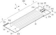
도 1은 연장된 상태의 본 발명에 따른 집속형 플렉서블 플랫 회로 케이블에 관한 사시도이다.
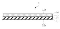
도 2는 도 1에서의 2-2 선에 따른 단면을 나타낸 단면도이다.
도 3은 본 발명에 따라 양면 회로 기판으로 형성된 플렉서블 기판의 단면도이다.
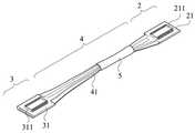
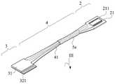
도 4는 적층 구조의 터미널 연결 섹션을 가지는 본 발명의 집속형 플렉서블 플랫 회로 케이블에 관한 사시도이다.
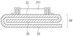
도 5는 도 4에서의 5-5 선에 따른 단면을 나타낸 단면도이다.
도 6은 본 발명의 일 실시형태에 따라 제1 연결 섹션과 제2 연결 섹션에 각각의 연결 소켓이 구비된 상태를 나타내는 본 발명에 따른 집속형 플렉서블 플랫 회로 케이블에 관한 사시도이다.
도 7은 본 발명의 일 실시형태에 따라 연결 섹션이 각각 2개의 분리된 클러스터 섹션의 클러스터 스트립을 통해 2개의 대향 연결 섹션에 연결된 상태를 나타내는 본 발명에 따른 집속형 플렉서블 플랫 회로 케이블에 관한 사시도이다.
도 8은 본 발명에 따른 플레서블 기판 상의 클러스터 섹션의 클러스터 스트립을 둘러싼 집속 구조체의 단면도이다.
도 9는 힌지 구조를 갖는 휴대 전화에 본 발명을 적용한 상태를 나타내는 사시도이다.
도 10은 도 8에 도시된 집속 구조체에서 차폐층의 외부 표면을 랩핑한 외부 절연층을 나타내는 단면도이다.
도 11은 절연층, 내부 절연층의 외부 표면을 랩핑한 차폐층 및 상기 차폐층의 외부 표면을 랩핑한 외부 절연층에 의해 랩핑된 본 발명의 플렉서블 기판의 클러스터 섹션을 나타내는 단면도이다.
도 12는 집속형 플렉서블 플랫 회로 케이블의 클러스터 섹션의 예정된 지점의 주변을 나선형의 집속 구조체가 랩핑한 상태를 나타내는 본 발명의 집속형 플렉서블 플랫 회로 케이블에 관한 사시도이다.1 is a perspective view of a focused flexible flat circuit cable according to the present invention in an extended state;
2 is a cross-sectional view taken along line 2-2 in Fig.
3 is a cross-sectional view of a flexible substrate formed of a double-sided circuit board according to the present invention.
4 is a perspective view of a focusing flexible flat circuit cable of the present invention having a terminal connection section of a laminated structure.
5 is a cross-sectional view taken along the line 5-5 in Fig.
6 is a perspective view of a focusing type flexible flat circuit cable according to an embodiment of the present invention, showing a state in which a first connection section and a second connection section are provided with respective connection sockets;
Figure 7 is a perspective view of a focused flexible flat circuit cable according to an embodiment of the present invention showing a connection section connected to two opposing connection sections through a cluster strip of two separate cluster sections, .
8 is a cross-sectional view of a focusing structure surrounding a cluster strip of cluster sections on a flexible substrate in accordance with the present invention.
9 is a perspective view showing a state in which the present invention is applied to a cellular phone having a hinge structure.
10 is a cross-sectional view showing an outer insulating layer wrapping the outer surface of the shielding layer in the focusing structure shown in Fig.
11 is a cross-sectional view illustrating a cluster section of a flexible substrate of the present invention wrapped by an insulating layer, a shielding layer wrapping the outer surface of the inner insulating layer, and an outer insulating layer wrapping the outer surface of the shielding layer.
Fig. 12 is a perspective view of a focusable flexible flat circuit cable of the present invention showing a spiral focusing structure wrapped around a predetermined point of a cluster section of a focusing type flexible flat circuit cable. Fig.
이하에서 본 발명에 대해 상세히 설명한다.Hereinafter, the present invention will be described in detail.
도 1 및 도 2를 참조하면, 도면 부호 100으로 표시되는 본 발명에 따른 집속형 플렉서블 플랫 회로 케이블은 연장 방향(I)으로 예정된 길이만큼 연장된 플렉서블 기판(11)을 포함한다. 상기 플렉서블 기판(11)은 제1 표면(11a) 및 제2 대향 표면(11b)을 가진다. 제1 전도층(12) 및 제1 절연층(13)은 상기 플렉서블 기판(11)의 제1 표면(11a) 상에 순차적으로 형성된다. 본 발명의 바람직한 구체예에 있어서, 차폐층(14)이 상기 제1 절연층(13) 상에 더 형성된다. 상기 차폐층(14)은 선택적 및 국부적으로 상기 제1 절연층(13)의 외부 표면의 예정된 부분에 형성되어 전기 신호를 보호하기 위해 전자기파를 차단할 수 있다.Referring to FIGS. 1 and 2, a focusing flexible
도 2에 도시된 플렉서블 회로기판은 편면 회로기판의 구조를 갖는다. 그러나, 본 발명은 양면 회로기판도 적용할 수 있다. 양면 회로기판의 구조에 있어서, 제2 전도층(15) 및 제2 절연층(16)은 플렉서블 기판(11)의 제2 표면(11b)에 순차적으로 형성된다(도 3 참조). 또한, 상기 양면 회로기판의 구조에 신호 점퍼 구조체(signal jumper structure)가 더 추가될 수 있다. 예를 들어, 쓰로우 홀(through hole)(17)은 플렉서블 기판(11)의 예정된 지점의 제1 표면(11a) 및 제2 표면(11b) 모두를 관통하여 형성되며, 전도성 물질이 상기 쓰로우 홀(17)의 내부 표면에 형성되어 상기 플렉서블 기판(11)의 제1 표면(11a)과 제2 표면(11b)에서의 제1 전도층(12) 및 제2 전도층(15) 사이의 선택적인 신호 통신을 가능하게 한다. 양면 회로기판의 구조는 선택적으로 2개의 편면 회로 기판을 백-투-백 방식(back-to-back manner)으로 결합하여 형성될 수 있다.The flexible circuit board shown in Fig. 2 has a structure of a single-sided circuit board. However, the present invention can also be applied to a double-sided circuit board. In the structure of the double-sided circuit board, the second
플렉서블 기판(11)은 연장 방향(I)에 따라 제1 연결 섹션(2), 제2 연결 섹션(3) 및 제1 및 제2 연결 섹션(2, 3) 사이의 클러스터 섹션(4)으로 구분된다. 보다 구체적으로, 제1 연결 섹션(2)은 클러스터 섹션(4)의 말단부에 위치하며, 제2 연결 섹션(3)은 제1 연결 섹션의 반대방향에 있는 플렉서블 기판(11)의 다른 말단부에 위치한다.The
클러스터 섹션(4)은 연장 방향(I)으로 플렉서블 기판(11)을 절편하여 형성된 복수개의 클러스터 스트립(41)을 포함한다. 클러스터 스트립(41)의 전체 또는 일부는 제1 연결 섹션(2)과 제2 연결 섹션(3) 사이의 전기 신호의 전송 통로 역할을 하는 신호선으로 사용된다. 클러스터 섹션(4)은 전체 또는 일부 클러스터 스트립의 터미널들 중 적합한 지점에 복수개의 찢김 방지 구멍(tear stop hole)(214)을 선택적으로 형성하여 클러스터 스트립(41)이 플렉서블 기판(11)을 사용하거나 조립하는 과정에서 절편시 의도와 다르게 찢겨져 손상되는 것을 방지할 수 있다.The
제1 연결 섹션(2)은 적층 구조체(20)를 포함한다. 도 4 및 도 5를 참조하면, 상기 적층 구조체(20)는 제1 연결 섹션(2)을 중심부(21)와 중심부(21)의 반대편에 위치한 측면 적층부(22, 23)로 나눈다. 2개 측면의 측면 적층부(22, 23) 또는 중심부의 일측면 중 하나의 측면 적층부(22, 23)는 중심부(21)를 향하여 접힐 수 있는 실제 또는 가상의 접이선(212, 213)에 따라 접혀짐으로써 중심부(21)의 하부 또는 중심부(21)의 일부분 상에 적층된 측면 적층부(22, 23)를 가질 수 있다. 이러한 방식으로 플렉서블 기판(11)의 연장 방향(I)에 수직한 방향에 따라 측정된 제1 연결 섹션(2)의 폭은 감소된다. 제2 연결 섹션(3)에는 제2 연결 섹션(3)의 중심부(31)의 대향되는 측면에 위치한 2개의 측면 적층부(32, 33)가 중심부(31)의 하부 또는 중심부(31)의 일부분 상에 적층될 수 있는 유사한 적층 구조체가 형성될 수 있다. 이러한 적층 방식을 수행하여 도 4에 도시된 구조체가 형성될 수 있다.The first connection section (2) includes a laminated structure (20). 4 and 5, the laminated
본 발명의 한 실시형태에 있어서, 제1 연결 섹션(2) 및 제2 연결 섹션(3)에는 예정된 지점에 다른 종류의 연결 소켓 또는 터미널 플러그가 제공될 수 있다. 예를 들며, 도 1의 한 구체예에 도시된 바와 같이, 연결 소켓(211)은 제1 연결 섹션(2)의 중심부(21) 상에 고정되며, 제2 연결 섹션(3)의 측면 적층부(32)는 측면 모서리에 터미널 플러그(321)를 형성한다. 임의적 또는 선택적으로 제1 연결 섹션(2) 및 제2 연결 섹션(3) 사이에 동일한 타입의 연결 소켓 또는 터미널 플러그가 형성될 수 있다. 예를 들어, 도 6의 한 구체예에 도시된 바와 같이, 제1 연결 섹션(2)의 중심부(21)에는 연결 소켓(211)이 구비되며, 또한 제2 연결 섹션(3)의 측면 적층부(31)에도 연결 소켓(311)이 형성된다.In one embodiment of the present invention, the first connection section (2) and the second connection section (3) may be provided with connection sockets or terminal plugs of different kinds at predetermined points. 1, the
플렉서블 기판의 상기 연결 섹션과 클러스터 섹션은 1 대 1 방식으로 구성될 수 있으며, 선택적으로 1 대 다수 방식으로 구성될 수 있다. 예를 들어, 도 1의 구체예는 하나의 연결 섹션이 단일 클러스터 섹션에 의해 다른 연결 섹션과 연결된 구조를 나타낸다. 반면, 도 7의 구체예에서는 제2 연결 섹션(3)이 클러스터 섹션(4)의 클러스터 스트립(41)에 의해 제1 연결 섹션(2)에 연결되며, 또한 추가적인 클러스터 섹션(4a)의 클러스터 스트립(41a)에 의해 추가적인 제1 연결 섹션(2a)에 연결될 수 있는 다른 형태의 구조를 나타낸다. 이러한 구조들은 실제 응용에 있어서 필요에 따라 변화될 수 있다.The connection section and the cluster section of the flexible substrate may be configured in a one-to-one manner, and may optionally be configured in a one-to-many manner. For example, the embodiment of FIG. 1 shows a structure in which one connection section is connected to another connection section by a single cluster section. 7, the
본 발명의 한 구체예에 있어서, 플렉서블 기판(11)의 클러스터 섹션(4)을 예정된 지점에서 통합하거나 집속할 수 있는 하나 이상의 집속 구조체(5)가 제공되어, 클러스터 섹션(4)의 클러스터 스트립(41)을 함께 집속함으로써 집속 구조를 형성할 수 있다(도 4 참조). 도 8은 도 4의 8-8 선에 따른 측단면을 나타낸다. 본 발명의 바람직한 구체예에 있어서, 집속 구조체(5)는 차폐층(51)을 포함한다. 보다 상세하게는, 집속 구조체(5)는 클러스터 섹션(4)의 예정된 지점을 통합하는 차폐 물질로 형성된 구조체를 포함하며, 상기 클러스터 섹션(4)의 클러스터 스트립(41)을 함께 통합하거나 집속함으로서 집속 구조체를 형성함과 동시에 클러스터 섹션(4)에서 전자기 차폐 효과를 구현할 수 있다. 집속 구조체(5)는 선택적으로 (방수성을 가진 플라스틱 밴드와 같은) 절연 물질을 사용하여 형성될 수 있으며, 또한 전자기 차폐 물질과 절연 물질의 혼합물을 사용하여 집속 구조체를 형성할 수 있다.In one embodiment of the present invention, one or more focusing
도 9는 힌지 구조를 가지는 휴대전화에 본 발명이 응용된 한 구체예를 나타낸다. 도시된 바와 같이, 플렉서블한 집속형 플랫 회로 케이블(100)은 플렉서블 기판(11)의 클러스터 섹션(4)의 클러스터 스트립(41)과 함께 힌지 구조체(6)에 고정되며, 제1 연결 섹션(2) 및 제2 연결 섹션(3)은 각각 힌지 구조체(6)의 반대편 상에 고정된다. 집속 구조체(5)의 차폐층(51)에 의해 구현되는 전자기 차폐 효과와 함께, 클러스터 섹션(4)의 클러스터 스트립(41)을 전송 통로로 하여 전송되는 전기 신호에 영향을 주는 전자기 간섭 효과도 효과적으로 제거될 수 있다.Fig. 9 shows a specific example in which the present invention is applied to a cellular phone having a hinge structure. The flexible concentric
다른 구체예에 있어서, 차폐층(51)의 외부 표면은 외부 절연층(52)에 의해 랩핑(wrapping)될 수 있으며(도 10 참조), 또한 플렉서블 기판(11)의 클러스터 섹션(4)은 내부 절연층(53)에 의해 랩핑되며 이때 차폐층(51)은 내부 절연층(53)의 외부 표면 주변에 랩핑되고, 마지막으로 외부 절연층(54)은 차폐층(51)의 외부 표면 주변에 랩핑된다(도 11 참조).The outer surface of the
앞서 설명한 구체예에서 사용된 집속 구조체(5)는 얇은 시트 형태로 형성될 수 있으며, 상기 시트는 랩핑 방향(wrapping direction)(Ⅱ)으로 상기 클러스터 섹션의 예정된 지점 주변을 랩핑한다. 선택적으로, 나선형의 랩핑 구조체가 집속 구조체를 형성하는데 사용될 수 있다. 도 12에 도시된 바와 같이, 전자기 차폐 물질로 제조된 가늘고 긴 밴드가 경사 방향(Ⅲ)에 따라 클러스터 섹션(4)의 클러스터 스트립(41)을 나선형으로 랩핑하여 나선형의 집속 구조체(5a)를 형성한다. 상기 가늘고 긴 밴드는 전기적 전도성을 갖는 천, 은 호일, 알루미늄 호일, 구리 호일 및 전자기 차폐 특성을 나타내는 다른 금속 호일을 포함하는 전자기 차폐 물질을 사용하여 제조될 수 있다.The focusing
Claims (18)
Translated fromKorean상기 플렉서블 기판의 제1 표면 상에 형성된 제1 전도층;
상기 플렉서블 기판의 말단 상에 형성된 하나 이상의 제1 연결 섹션;
상기 제1 연결 섹션과 대향되는 플렉서블 기판의 대향 말단 상에 형성된 하나 이상의 제2 연결 섹션;
상기 제1 연결 섹션과 제2 연결 섹션 사이에 연결되며, 연장 방향으로 플렉서블 기판을 절단하여 형성된 복수개의 클러스터 스트립을 포함하는 하나 이상의 클러스터 섹션; 및
상기 클러스터 섹션의 클러스터 스트립을 랩핑하여 집속 구조를 형성할 수 있도록 상기 클러스터 섹션의 예정된 지점을 집속하는 하나 이상의 집속 구조체를 포함하며, 상기 집속 구조체는 상기 클러스터 섹션 주변을 랩핑하는 차폐층 및 상기 차폐층의 외부 표면 주변을 랩핑하는 외부 절연층을 포함하고,
상기 제1 연결 섹션 및 제2 연결 섹션 모두 또는 제1 연결 섹션과 제2 연결 섹션중 하나는 적층 구조체를 포함하며, 상기 적층 구조체는 2개 대향 측면 적층부나 상기 각각의 연결 섹션들의 2개의 대향 측면 적층부 중 하나를 각각의 접이선에 따라 접음으로써 형성되어 상기 2개의 대향 측면 적층부 사이에 위치한 상기 연결 섹션의 중심부의 적어도 일부분 상에 적층된 측면 적층부 또는 측면 적층부들을 가지게 되고,
상기 플렉서블 기판의 제1 표면은 상기 제1 전도층의 외부 표면 상에 형성된 제1 절연층 및 상기 제1 절연층 상에 형성된 차폐층을 포함하며,
상기 클러스터 스트립의 전체 또는 일부는 제1 연결 섹션 또는 제2 연결 섹션에 근접한 예정된 지점에 찢김 방지 구멍을 하나 이상 형성하는 것을 특징으로 하는 플렉서블한 집속형 플랫 회로 케이블.A flexible substrate having a first surface and a second surface and extending in an extending direction;
A first conductive layer formed on a first surface of the flexible substrate;
At least one first connection section formed on an end of the flexible substrate;
At least one second connection section formed on an opposite end of the flexible substrate facing the first connection section;
At least one cluster section connected between the first connection section and the second connection section and including a plurality of cluster strips formed by cutting the flexible substrate in the extending direction; And
At least one focusing structure for focusing a predetermined point of the cluster section so as to form a focusing structure by wrapping the cluster strip of the cluster section, the focusing structure comprising a shielding layer wrapping around the cluster section, And an outer insulating layer surrounding the outer surface of the insulating layer,
Wherein either one of the first connecting section and the second connecting section or one of the first connecting section and the second connecting section comprises a lamination structure comprising two opposing side lamination sections, A side laminated portion or side laminated portion formed by folding one of the laminated portions along each folding line and stacked on at least a part of the center portion of the connecting section located between the two opposing side laminated portions,
Wherein the first surface of the flexible substrate includes a first insulation layer formed on an outer surface of the first conductive layer and a shield layer formed on the first insulation layer,
Characterized in that all or part of the cluster strips form one or more anti-tearing apertures at predetermined points near the first connection section or the second connection section.
상기 플렉서블 기판의 제2 표면은 제2 전도층 및 상기 제2 전도층 상에 형성된 제2 절연층을 포함하는 것을 특징으로 하는 플렉서블한 집속형 플랫 회로 케이블.The method according to claim 1,
Wherein the second surface of the flexible substrate comprises a second conductive layer and a second insulation layer formed on the second conductive layer.
상기 집속 구조체는 클러스터 섹션의 예정된 지점 주변을 랩핑할 수 있도록 차폐 물질 또는 절연 물질 중 하나를 사용하여 형성된, 차폐효과를 갖는 집속 구조체를 포함하는 것을 특징으로 하는 플렉서블한 집속형 플랫 회로 케이블.The method according to claim 1,
Wherein the focusing structure includes a focusing structure having a shielding effect, formed using one of a shielding material or an insulating material so as to be able to wrap around a predetermined point of the cluster section.
상기 집속 구조체는 클러스터 섹션 주변을 랩핑하는 내부 절연층 및 상기 내부 절연층의 외부 표면 주변을 랩핑하는 차폐층을 포함하는 것을 특징으로 하는 플렉서블한 집속형 플랫 회로 케이블.The method according to claim 1,
Wherein the focusing structure comprises an inner insulating layer wrapping around the cluster section and a shielding layer wrapping around the outer surface of the inner insulating layer.
상기 차폐층은 외부 절연층에 의해 외부 표면이 랩핑되는 것을 특징으로 하는 플렉서블한 집속형 플랫 회로 케이블.The method of claim 5,
Wherein the shielding layer is wrapped with an outer surface by an outer insulating layer.
상기 플렉서블 기판의 제1 표면 상에 형성된 제1 전도층;
상기 플렉서블 기판의 말단에 형성된 하나 이상의 제1 연결 섹션;
상기 제1 연결 섹션과 대향되도록 플렉서블 기판의 반대 말단 상에 형성된 하나 이상의 제2 연결 섹션;
상기 제1 연결 섹션과 제2 연결 섹션 사이에 연결되며, 연장 방향으로 플렉서블 기판을 절단하여 형성된 복수개의 클러스터 스트립을 포함하는 하나 이상의 클러스터 섹션;
상기 제1 전도층 상에 형성된 제1 절연층;
상기 제1 절연층 상에 형성된 전자기 차폐층; 및
상기 클러스터 섹션의 클러스터 스트립을 랩핑하여 집속 구조를 형성할 수 있도록 예정된 지점의 상기 클러스터 섹션을 집속하는 하나 이상의 집속 구조체를 포함하고, 상기 집속 구조체는 상기 클러스터 섹션 주변을 랩핑하는 전자기 차폐층 및 상기 전자기 차폐층의 외부 표면 주변을 랩핑하는 외부 절연층을 포함하며,
상기 클러스터 스트립의 전체 또는 일부는 제1 연결 섹션 또는 제2 연결 섹션에 근접한 예정된 지점에 찢김 방지 구멍을 하나 이상 형성하는 것을 특징으로 하는 플렉서블한 집속형 플랫 회로 케이블.A flexible substrate having a first surface and a second surface and extending in an extending direction;
A first conductive layer formed on a first surface of the flexible substrate;
At least one first connection section formed at an end of the flexible substrate;
At least one second connection section formed on the opposite end of the flexible substrate so as to face the first connection section;
At least one cluster section connected between the first connection section and the second connection section and including a plurality of cluster strips formed by cutting the flexible substrate in the extending direction;
A first insulating layer formed on the first conductive layer;
An electromagnetic shielding layer formed on the first insulating layer; And
And at least one focusing structure for focusing the cluster section at a predetermined point so as to form a focusing structure by lapping the cluster strips of the cluster section, the focusing structure including an electromagnetic shielding layer wrapping around the cluster section, And an outer insulating layer wrapping around the outer surface of the shield layer,
Characterized in that all or part of the cluster strips form one or more anti-tearing apertures at predetermined points near the first connection section or the second connection section.
상기 플렉서블 기판의 제2 표면은 제2 전도층 및 상기 제2 전도층 상에 형성된 제2 절연층을 포함하는 것을 특징으로 하는 플렉서블한 집속형 플랫 회로 케이블.The method of claim 12,
Wherein the second surface of the flexible substrate comprises a second conductive layer and a second insulation layer formed on the second conductive layer.
상기 집속 구조체는 클러스터 섹션의 예정된 지점 주변을 랩핑할 수 있도록 차폐 물질 또는 절연 물질 중 하나를 사용하여 형성된, 차폐효과를 갖는 집속 구조체를 포함하는 것을 특징으로 하는 플렉서블한 집속형 플랫 회로 케이블.The method of claim 12,
Wherein the focusing structure includes a focusing structure having a shielding effect, formed using one of a shielding material or an insulating material so as to be able to wrap around a predetermined point of the cluster section.
상기 집속 구조체는 클러스터 섹션 주변을 랩핑하는 내부 절연층 및 상기 내부 절연층의 외부 표면 주변을 랩핑하는 전자기 차폐층을 포함하는 것을 특징으로 하는 플렉서블한 집속형 플랫 회로 케이블.The method of claim 12,
Wherein the focusing structure includes an inner insulating layer wrapping around the cluster section and an electromagnetic shielding layer wrapping around the outer surface of the inner insulating layer.
상기 전자기 차폐층은 외부 절연층에 의해 외부 표면이 랩핑되는 것을 특징으로 하는 플렉서블한 집속형 플랫 회로 케이블.16. The method of claim 15,
Wherein the electromagnetic shielding layer is wrapped with an outer surface by an outer insulating layer.
Applications Claiming Priority (2)
| Application Number | Priority Date | Filing Date | Title |
|---|---|---|---|
| TW98131522 | 2009-09-18 | ||
| TW098131522ATWI543209B (en) | 2009-09-18 | 2009-09-18 | Bundled soft circuit cable |
Publications (2)
| Publication Number | Publication Date |
|---|---|
| KR20110031074A KR20110031074A (en) | 2011-03-24 |
| KR101664241B1true KR101664241B1 (en) | 2016-10-10 |
Family
ID=43755649
Family Applications (1)
| Application Number | Title | Priority Date | Filing Date |
|---|---|---|---|
| KR1020100030311AActiveKR101664241B1 (en) | 2009-09-18 | 2010-04-02 | Bundled flexible flat circuit cable |
Country Status (4)
| Country | Link |
|---|---|
| US (4) | US20110067903A1 (en) |
| JP (1) | JP5491906B2 (en) |
| KR (1) | KR101664241B1 (en) |
| TW (1) | TWI543209B (en) |
Cited By (2)
| Publication number | Priority date | Publication date | Assignee | Title |
|---|---|---|---|---|
| KR20200092031A (en) | 2019-01-24 | 2020-08-03 | 주식회사 아모그린텍 | Flexible Cable Jumper Structure Body and Manufacturing Method For The Same |
| KR20200117165A (en) | 2019-04-03 | 2020-10-14 | 주식회사 아모센스 | Flexible Cable Jumper Apparatus and Manufacturing Method For The Same |
Families Citing this family (186)
| Publication number | Priority date | Publication date | Assignee | Title |
|---|---|---|---|---|
| JP2011066086A (en)* | 2009-09-15 | 2011-03-31 | Toshiba Corp | Flexible wiring board array, method of manufacturing the same, and flexible wiring device |
| US20110122323A1 (en)* | 2009-11-26 | 2011-05-26 | Samsung Electronics Co., Ltd. | Flat cable and display apparatus including the same |
| TWI537990B (en)* | 2012-05-25 | 2016-06-11 | Adv Flexible Circuits Co Ltd | A soft circuit cable with two or more groups of clusters |
| TWI453768B (en)* | 2012-06-20 | 2014-09-21 | Adv Flexible Circuits Co Ltd | Composite flexible circuit cable |
| TW201415743A (en)* | 2012-10-09 | 2014-04-16 | Adv Flexible Circuits Co Ltd | Beam structure of flexible circuit cable |
| US9113347B2 (en) | 2012-12-05 | 2015-08-18 | At&T Intellectual Property I, Lp | Backhaul link for distributed antenna system |
| US10009065B2 (en) | 2012-12-05 | 2018-06-26 | At&T Intellectual Property I, L.P. | Backhaul link for distributed antenna system |
| CN103885531A (en)* | 2012-12-22 | 2014-06-25 | 鸿富锦精密工业(深圳)有限公司 | Electronic equipment connecting device |
| US9781825B2 (en)* | 2013-02-18 | 2017-10-03 | Dell Products L.P. | Flex circuit, an information handling system, and a method of manufacturing a flexible circuit |
| US9974187B2 (en)* | 2013-04-22 | 2018-05-15 | Infineon Technologies Austria Ag | Power in lead |
| US9999038B2 (en) | 2013-05-31 | 2018-06-12 | At&T Intellectual Property I, L.P. | Remote distributed antenna system |
| US9525524B2 (en) | 2013-05-31 | 2016-12-20 | At&T Intellectual Property I, L.P. | Remote distributed antenna system |
| TWI637669B (en)* | 2013-07-12 | 2018-10-01 | 易鼎股份有限公司 | Wearable assembly method of flexible circuit board and shaft member |
| TWI590721B (en)* | 2013-07-26 | 2017-07-01 | Adv Flexible Circuits Co Ltd | The flexible circuit board with the wings and the shaft assembly structure |
| US8897697B1 (en) | 2013-11-06 | 2014-11-25 | At&T Intellectual Property I, Lp | Millimeter-wave surface-wave communications |
| US9209902B2 (en) | 2013-12-10 | 2015-12-08 | At&T Intellectual Property I, L.P. | Quasi-optical coupler |
| TWI622328B (en)* | 2014-03-03 | 2018-04-21 | Stretchable flexible circuit board | |
| TWI573503B (en)* | 2014-06-09 | 2017-03-01 | The Power Supply Path Structure of Soft Circuit Board | |
| US9692101B2 (en) | 2014-08-26 | 2017-06-27 | At&T Intellectual Property I, L.P. | Guided wave couplers for coupling electromagnetic waves between a waveguide surface and a surface of a wire |
| US9768833B2 (en) | 2014-09-15 | 2017-09-19 | At&T Intellectual Property I, L.P. | Method and apparatus for sensing a condition in a transmission medium of electromagnetic waves |
| US10063280B2 (en) | 2014-09-17 | 2018-08-28 | At&T Intellectual Property I, L.P. | Monitoring and mitigating conditions in a communication network |
| US9628854B2 (en) | 2014-09-29 | 2017-04-18 | At&T Intellectual Property I, L.P. | Method and apparatus for distributing content in a communication network |
| US9615269B2 (en) | 2014-10-02 | 2017-04-04 | At&T Intellectual Property I, L.P. | Method and apparatus that provides fault tolerance in a communication network |
| US9685992B2 (en) | 2014-10-03 | 2017-06-20 | At&T Intellectual Property I, L.P. | Circuit panel network and methods thereof |
| US9503189B2 (en) | 2014-10-10 | 2016-11-22 | At&T Intellectual Property I, L.P. | Method and apparatus for arranging communication sessions in a communication system |
| US9762289B2 (en) | 2014-10-14 | 2017-09-12 | At&T Intellectual Property I, L.P. | Method and apparatus for transmitting or receiving signals in a transportation system |
| US9973299B2 (en) | 2014-10-14 | 2018-05-15 | At&T Intellectual Property I, L.P. | Method and apparatus for adjusting a mode of communication in a communication network |
| US9627768B2 (en) | 2014-10-21 | 2017-04-18 | At&T Intellectual Property I, L.P. | Guided-wave transmission device with non-fundamental mode propagation and methods for use therewith |
| US9564947B2 (en) | 2014-10-21 | 2017-02-07 | At&T Intellectual Property I, L.P. | Guided-wave transmission device with diversity and methods for use therewith |
| US9312919B1 (en) | 2014-10-21 | 2016-04-12 | At&T Intellectual Property I, Lp | Transmission device with impairment compensation and methods for use therewith |
| US9780834B2 (en) | 2014-10-21 | 2017-10-03 | At&T Intellectual Property I, L.P. | Method and apparatus for transmitting electromagnetic waves |
| US9520945B2 (en) | 2014-10-21 | 2016-12-13 | At&T Intellectual Property I, L.P. | Apparatus for providing communication services and methods thereof |
| US9577306B2 (en) | 2014-10-21 | 2017-02-21 | At&T Intellectual Property I, L.P. | Guided-wave transmission device and methods for use therewith |
| US9769020B2 (en) | 2014-10-21 | 2017-09-19 | At&T Intellectual Property I, L.P. | Method and apparatus for responding to events affecting communications in a communication network |
| US9653770B2 (en) | 2014-10-21 | 2017-05-16 | At&T Intellectual Property I, L.P. | Guided wave coupler, coupling module and methods for use therewith |
| US9742462B2 (en) | 2014-12-04 | 2017-08-22 | At&T Intellectual Property I, L.P. | Transmission medium and communication interfaces and methods for use therewith |
| US9461706B1 (en) | 2015-07-31 | 2016-10-04 | At&T Intellectual Property I, Lp | Method and apparatus for exchanging communication signals |
| US9544006B2 (en) | 2014-11-20 | 2017-01-10 | At&T Intellectual Property I, L.P. | Transmission device with mode division multiplexing and methods for use therewith |
| US10009067B2 (en) | 2014-12-04 | 2018-06-26 | At&T Intellectual Property I, L.P. | Method and apparatus for configuring a communication interface |
| US10340573B2 (en) | 2016-10-26 | 2019-07-02 | At&T Intellectual Property I, L.P. | Launcher with cylindrical coupling device and methods for use therewith |
| US10243784B2 (en) | 2014-11-20 | 2019-03-26 | At&T Intellectual Property I, L.P. | System for generating topology information and methods thereof |
| US9997819B2 (en) | 2015-06-09 | 2018-06-12 | At&T Intellectual Property I, L.P. | Transmission medium and method for facilitating propagation of electromagnetic waves via a core |
| US9680670B2 (en) | 2014-11-20 | 2017-06-13 | At&T Intellectual Property I, L.P. | Transmission device with channel equalization and control and methods for use therewith |
| US9954287B2 (en) | 2014-11-20 | 2018-04-24 | At&T Intellectual Property I, L.P. | Apparatus for converting wireless signals and electromagnetic waves and methods thereof |
| US9800327B2 (en) | 2014-11-20 | 2017-10-24 | At&T Intellectual Property I, L.P. | Apparatus for controlling operations of a communication device and methods thereof |
| US9654173B2 (en) | 2014-11-20 | 2017-05-16 | At&T Intellectual Property I, L.P. | Apparatus for powering a communication device and methods thereof |
| US10144036B2 (en) | 2015-01-30 | 2018-12-04 | At&T Intellectual Property I, L.P. | Method and apparatus for mitigating interference affecting a propagation of electromagnetic waves guided by a transmission medium |
| US9876570B2 (en) | 2015-02-20 | 2018-01-23 | At&T Intellectual Property I, Lp | Guided-wave transmission device with non-fundamental mode propagation and methods for use therewith |
| US9749013B2 (en) | 2015-03-17 | 2017-08-29 | At&T Intellectual Property I, L.P. | Method and apparatus for reducing attenuation of electromagnetic waves guided by a transmission medium |
| US9705561B2 (en) | 2015-04-24 | 2017-07-11 | At&T Intellectual Property I, L.P. | Directional coupling device and methods for use therewith |
| US10224981B2 (en) | 2015-04-24 | 2019-03-05 | At&T Intellectual Property I, Lp | Passive electrical coupling device and methods for use therewith |
| US9948354B2 (en) | 2015-04-28 | 2018-04-17 | At&T Intellectual Property I, L.P. | Magnetic coupling device with reflective plate and methods for use therewith |
| US9793954B2 (en) | 2015-04-28 | 2017-10-17 | At&T Intellectual Property I, L.P. | Magnetic coupling device and methods for use therewith |
| US9871282B2 (en) | 2015-05-14 | 2018-01-16 | At&T Intellectual Property I, L.P. | At least one transmission medium having a dielectric surface that is covered at least in part by a second dielectric |
| US9748626B2 (en) | 2015-05-14 | 2017-08-29 | At&T Intellectual Property I, L.P. | Plurality of cables having different cross-sectional shapes which are bundled together to form a transmission medium |
| US9490869B1 (en) | 2015-05-14 | 2016-11-08 | At&T Intellectual Property I, L.P. | Transmission medium having multiple cores and methods for use therewith |
| US10650940B2 (en) | 2015-05-15 | 2020-05-12 | At&T Intellectual Property I, L.P. | Transmission medium having a conductive material and methods for use therewith |
| US10679767B2 (en) | 2015-05-15 | 2020-06-09 | At&T Intellectual Property I, L.P. | Transmission medium having a conductive material and methods for use therewith |
| US9917341B2 (en) | 2015-05-27 | 2018-03-13 | At&T Intellectual Property I, L.P. | Apparatus and method for launching electromagnetic waves and for modifying radial dimensions of the propagating electromagnetic waves |
| US10154493B2 (en) | 2015-06-03 | 2018-12-11 | At&T Intellectual Property I, L.P. | Network termination and methods for use therewith |
| US10348391B2 (en) | 2015-06-03 | 2019-07-09 | At&T Intellectual Property I, L.P. | Client node device with frequency conversion and methods for use therewith |
| US10103801B2 (en) | 2015-06-03 | 2018-10-16 | At&T Intellectual Property I, L.P. | Host node device and methods for use therewith |
| US9866309B2 (en) | 2015-06-03 | 2018-01-09 | At&T Intellectual Property I, Lp | Host node device and methods for use therewith |
| US10812174B2 (en) | 2015-06-03 | 2020-10-20 | At&T Intellectual Property I, L.P. | Client node device and methods for use therewith |
| US9912381B2 (en) | 2015-06-03 | 2018-03-06 | At&T Intellectual Property I, Lp | Network termination and methods for use therewith |
| US9913139B2 (en) | 2015-06-09 | 2018-03-06 | At&T Intellectual Property I, L.P. | Signal fingerprinting for authentication of communicating devices |
| US9608692B2 (en) | 2015-06-11 | 2017-03-28 | At&T Intellectual Property I, L.P. | Repeater and methods for use therewith |
| US10142086B2 (en) | 2015-06-11 | 2018-11-27 | At&T Intellectual Property I, L.P. | Repeater and methods for use therewith |
| US9820146B2 (en) | 2015-06-12 | 2017-11-14 | At&T Intellectual Property I, L.P. | Method and apparatus for authentication and identity management of communicating devices |
| US9667317B2 (en) | 2015-06-15 | 2017-05-30 | At&T Intellectual Property I, L.P. | Method and apparatus for providing security using network traffic adjustments |
| US9509415B1 (en) | 2015-06-25 | 2016-11-29 | At&T Intellectual Property I, L.P. | Methods and apparatus for inducing a fundamental wave mode on a transmission medium |
| US9640850B2 (en) | 2015-06-25 | 2017-05-02 | At&T Intellectual Property I, L.P. | Methods and apparatus for inducing a non-fundamental wave mode on a transmission medium |
| US9865911B2 (en) | 2015-06-25 | 2018-01-09 | At&T Intellectual Property I, L.P. | Waveguide system for slot radiating first electromagnetic waves that are combined into a non-fundamental wave mode second electromagnetic wave on a transmission medium |
| US10148016B2 (en) | 2015-07-14 | 2018-12-04 | At&T Intellectual Property I, L.P. | Apparatus and methods for communicating utilizing an antenna array |
| US10205655B2 (en) | 2015-07-14 | 2019-02-12 | At&T Intellectual Property I, L.P. | Apparatus and methods for communicating utilizing an antenna array and multiple communication paths |
| US9836957B2 (en) | 2015-07-14 | 2017-12-05 | At&T Intellectual Property I, L.P. | Method and apparatus for communicating with premises equipment |
| US9847566B2 (en) | 2015-07-14 | 2017-12-19 | At&T Intellectual Property I, L.P. | Method and apparatus for adjusting a field of a signal to mitigate interference |
| US9853342B2 (en) | 2015-07-14 | 2017-12-26 | At&T Intellectual Property I, L.P. | Dielectric transmission medium connector and methods for use therewith |
| US10341142B2 (en) | 2015-07-14 | 2019-07-02 | At&T Intellectual Property I, L.P. | Apparatus and methods for generating non-interfering electromagnetic waves on an uninsulated conductor |
| US10044409B2 (en) | 2015-07-14 | 2018-08-07 | At&T Intellectual Property I, L.P. | Transmission medium and methods for use therewith |
| US9882257B2 (en) | 2015-07-14 | 2018-01-30 | At&T Intellectual Property I, L.P. | Method and apparatus for launching a wave mode that mitigates interference |
| US10033107B2 (en) | 2015-07-14 | 2018-07-24 | At&T Intellectual Property I, L.P. | Method and apparatus for coupling an antenna to a device |
| US10033108B2 (en) | 2015-07-14 | 2018-07-24 | At&T Intellectual Property I, L.P. | Apparatus and methods for generating an electromagnetic wave having a wave mode that mitigates interference |
| US9722318B2 (en) | 2015-07-14 | 2017-08-01 | At&T Intellectual Property I, L.P. | Method and apparatus for coupling an antenna to a device |
| US9628116B2 (en) | 2015-07-14 | 2017-04-18 | At&T Intellectual Property I, L.P. | Apparatus and methods for transmitting wireless signals |
| US10320586B2 (en) | 2015-07-14 | 2019-06-11 | At&T Intellectual Property I, L.P. | Apparatus and methods for generating non-interfering electromagnetic waves on an insulated transmission medium |
| US10170840B2 (en) | 2015-07-14 | 2019-01-01 | At&T Intellectual Property I, L.P. | Apparatus and methods for sending or receiving electromagnetic signals |
| US9793951B2 (en) | 2015-07-15 | 2017-10-17 | At&T Intellectual Property I, L.P. | Method and apparatus for launching a wave mode that mitigates interference |
| US10090606B2 (en) | 2015-07-15 | 2018-10-02 | At&T Intellectual Property I, L.P. | Antenna system with dielectric array and methods for use therewith |
| US9608740B2 (en) | 2015-07-15 | 2017-03-28 | At&T Intellectual Property I, L.P. | Method and apparatus for launching a wave mode that mitigates interference |
| US9749053B2 (en) | 2015-07-23 | 2017-08-29 | At&T Intellectual Property I, L.P. | Node device, repeater and methods for use therewith |
| US10784670B2 (en) | 2015-07-23 | 2020-09-22 | At&T Intellectual Property I, L.P. | Antenna support for aligning an antenna |
| US9948333B2 (en) | 2015-07-23 | 2018-04-17 | At&T Intellectual Property I, L.P. | Method and apparatus for wireless communications to mitigate interference |
| US9912027B2 (en) | 2015-07-23 | 2018-03-06 | At&T Intellectual Property I, L.P. | Method and apparatus for exchanging communication signals |
| US9871283B2 (en) | 2015-07-23 | 2018-01-16 | At&T Intellectual Property I, Lp | Transmission medium having a dielectric core comprised of plural members connected by a ball and socket configuration |
| US9735833B2 (en) | 2015-07-31 | 2017-08-15 | At&T Intellectual Property I, L.P. | Method and apparatus for communications management in a neighborhood network |
| US9967173B2 (en) | 2015-07-31 | 2018-05-08 | At&T Intellectual Property I, L.P. | Method and apparatus for authentication and identity management of communicating devices |
| US10020587B2 (en) | 2015-07-31 | 2018-07-10 | At&T Intellectual Property I, L.P. | Radial antenna and methods for use therewith |
| US9904535B2 (en) | 2015-09-14 | 2018-02-27 | At&T Intellectual Property I, L.P. | Method and apparatus for distributing software |
| US10009901B2 (en) | 2015-09-16 | 2018-06-26 | At&T Intellectual Property I, L.P. | Method, apparatus, and computer-readable storage medium for managing utilization of wireless resources between base stations |
| US9705571B2 (en) | 2015-09-16 | 2017-07-11 | At&T Intellectual Property I, L.P. | Method and apparatus for use with a radio distributed antenna system |
| US10079661B2 (en) | 2015-09-16 | 2018-09-18 | At&T Intellectual Property I, L.P. | Method and apparatus for use with a radio distributed antenna system having a clock reference |
| US10051629B2 (en) | 2015-09-16 | 2018-08-14 | At&T Intellectual Property I, L.P. | Method and apparatus for use with a radio distributed antenna system having an in-band reference signal |
| US10136434B2 (en) | 2015-09-16 | 2018-11-20 | At&T Intellectual Property I, L.P. | Method and apparatus for use with a radio distributed antenna system having an ultra-wideband control channel |
| US10009063B2 (en) | 2015-09-16 | 2018-06-26 | At&T Intellectual Property I, L.P. | Method and apparatus for use with a radio distributed antenna system having an out-of-band reference signal |
| US9769128B2 (en) | 2015-09-28 | 2017-09-19 | At&T Intellectual Property I, L.P. | Method and apparatus for encryption of communications over a network |
| US9729197B2 (en) | 2015-10-01 | 2017-08-08 | At&T Intellectual Property I, L.P. | Method and apparatus for communicating network management traffic over a network |
| US9882277B2 (en) | 2015-10-02 | 2018-01-30 | At&T Intellectual Property I, Lp | Communication device and antenna assembly with actuated gimbal mount |
| US10074890B2 (en) | 2015-10-02 | 2018-09-11 | At&T Intellectual Property I, L.P. | Communication device and antenna with integrated light assembly |
| US9876264B2 (en) | 2015-10-02 | 2018-01-23 | At&T Intellectual Property I, Lp | Communication system, guided wave switch and methods for use therewith |
| US10665942B2 (en) | 2015-10-16 | 2020-05-26 | At&T Intellectual Property I, L.P. | Method and apparatus for adjusting wireless communications |
| US10051483B2 (en) | 2015-10-16 | 2018-08-14 | At&T Intellectual Property I, L.P. | Method and apparatus for directing wireless signals |
| US10355367B2 (en) | 2015-10-16 | 2019-07-16 | At&T Intellectual Property I, L.P. | Antenna structure for exchanging wireless signals |
| TWI678847B (en)* | 2016-04-28 | 2019-12-01 | 易鼎股份有限公司 | Corresponding overlapping connection structure with flexible circuit carrier board |
| US10382659B2 (en)* | 2016-07-05 | 2019-08-13 | Hanwha Techwin Co., Ltd. | Surveillance camera system |
| US9912419B1 (en) | 2016-08-24 | 2018-03-06 | At&T Intellectual Property I, L.P. | Method and apparatus for managing a fault in a distributed antenna system |
| US9860075B1 (en) | 2016-08-26 | 2018-01-02 | At&T Intellectual Property I, L.P. | Method and communication node for broadband distribution |
| US10291311B2 (en) | 2016-09-09 | 2019-05-14 | At&T Intellectual Property I, L.P. | Method and apparatus for mitigating a fault in a distributed antenna system |
| US11032819B2 (en) | 2016-09-15 | 2021-06-08 | At&T Intellectual Property I, L.P. | Method and apparatus for use with a radio distributed antenna system having a control channel reference signal |
| US10340600B2 (en) | 2016-10-18 | 2019-07-02 | At&T Intellectual Property I, L.P. | Apparatus and methods for launching guided waves via plural waveguide systems |
| US10135146B2 (en) | 2016-10-18 | 2018-11-20 | At&T Intellectual Property I, L.P. | Apparatus and methods for launching guided waves via circuits |
| US10135147B2 (en) | 2016-10-18 | 2018-11-20 | At&T Intellectual Property I, L.P. | Apparatus and methods for launching guided waves via an antenna |
| US10374316B2 (en) | 2016-10-21 | 2019-08-06 | At&T Intellectual Property I, L.P. | System and dielectric antenna with non-uniform dielectric |
| US9876605B1 (en) | 2016-10-21 | 2018-01-23 | At&T Intellectual Property I, L.P. | Launcher and coupling system to support desired guided wave mode |
| US10811767B2 (en) | 2016-10-21 | 2020-10-20 | At&T Intellectual Property I, L.P. | System and dielectric antenna with convex dielectric radome |
| US9991580B2 (en) | 2016-10-21 | 2018-06-05 | At&T Intellectual Property I, L.P. | Launcher and coupling system for guided wave mode cancellation |
| US10312567B2 (en) | 2016-10-26 | 2019-06-04 | At&T Intellectual Property I, L.P. | Launcher with planar strip antenna and methods for use therewith |
| US10225025B2 (en) | 2016-11-03 | 2019-03-05 | At&T Intellectual Property I, L.P. | Method and apparatus for detecting a fault in a communication system |
| US10291334B2 (en) | 2016-11-03 | 2019-05-14 | At&T Intellectual Property I, L.P. | System for detecting a fault in a communication system |
| US10224634B2 (en) | 2016-11-03 | 2019-03-05 | At&T Intellectual Property I, L.P. | Methods and apparatus for adjusting an operational characteristic of an antenna |
| US10498044B2 (en) | 2016-11-03 | 2019-12-03 | At&T Intellectual Property I, L.P. | Apparatus for configuring a surface of an antenna |
| US10178445B2 (en) | 2016-11-23 | 2019-01-08 | At&T Intellectual Property I, L.P. | Methods, devices, and systems for load balancing between a plurality of waveguides |
| US10090594B2 (en) | 2016-11-23 | 2018-10-02 | At&T Intellectual Property I, L.P. | Antenna system having structural configurations for assembly |
| US10340601B2 (en) | 2016-11-23 | 2019-07-02 | At&T Intellectual Property I, L.P. | Multi-antenna system and methods for use therewith |
| US10340603B2 (en) | 2016-11-23 | 2019-07-02 | At&T Intellectual Property I, L.P. | Antenna system having shielded structural configurations for assembly |
| US10535928B2 (en) | 2016-11-23 | 2020-01-14 | At&T Intellectual Property I, L.P. | Antenna system and methods for use therewith |
| US10361489B2 (en) | 2016-12-01 | 2019-07-23 | At&T Intellectual Property I, L.P. | Dielectric dish antenna system and methods for use therewith |
| US10305190B2 (en) | 2016-12-01 | 2019-05-28 | At&T Intellectual Property I, L.P. | Reflecting dielectric antenna system and methods for use therewith |
| US10727599B2 (en) | 2016-12-06 | 2020-07-28 | At&T Intellectual Property I, L.P. | Launcher with slot antenna and methods for use therewith |
| US10020844B2 (en) | 2016-12-06 | 2018-07-10 | T&T Intellectual Property I, L.P. | Method and apparatus for broadcast communication via guided waves |
| US10326494B2 (en) | 2016-12-06 | 2019-06-18 | At&T Intellectual Property I, L.P. | Apparatus for measurement de-embedding and methods for use therewith |
| US10637149B2 (en) | 2016-12-06 | 2020-04-28 | At&T Intellectual Property I, L.P. | Injection molded dielectric antenna and methods for use therewith |
| US10382976B2 (en) | 2016-12-06 | 2019-08-13 | At&T Intellectual Property I, L.P. | Method and apparatus for managing wireless communications based on communication paths and network device positions |
| US10439675B2 (en) | 2016-12-06 | 2019-10-08 | At&T Intellectual Property I, L.P. | Method and apparatus for repeating guided wave communication signals |
| US9927517B1 (en) | 2016-12-06 | 2018-03-27 | At&T Intellectual Property I, L.P. | Apparatus and methods for sensing rainfall |
| US10819035B2 (en) | 2016-12-06 | 2020-10-27 | At&T Intellectual Property I, L.P. | Launcher with helical antenna and methods for use therewith |
| US10755542B2 (en) | 2016-12-06 | 2020-08-25 | At&T Intellectual Property I, L.P. | Method and apparatus for surveillance via guided wave communication |
| US10694379B2 (en) | 2016-12-06 | 2020-06-23 | At&T Intellectual Property I, L.P. | Waveguide system with device-based authentication and methods for use therewith |
| US10135145B2 (en) | 2016-12-06 | 2018-11-20 | At&T Intellectual Property I, L.P. | Apparatus and methods for generating an electromagnetic wave along a transmission medium |
| US10243270B2 (en) | 2016-12-07 | 2019-03-26 | At&T Intellectual Property I, L.P. | Beam adaptive multi-feed dielectric antenna system and methods for use therewith |
| US10446936B2 (en) | 2016-12-07 | 2019-10-15 | At&T Intellectual Property I, L.P. | Multi-feed dielectric antenna system and methods for use therewith |
| US9893795B1 (en) | 2016-12-07 | 2018-02-13 | At&T Intellectual Property I, Lp | Method and repeater for broadband distribution |
| US10139820B2 (en) | 2016-12-07 | 2018-11-27 | At&T Intellectual Property I, L.P. | Method and apparatus for deploying equipment of a communication system |
| US10168695B2 (en) | 2016-12-07 | 2019-01-01 | At&T Intellectual Property I, L.P. | Method and apparatus for controlling an unmanned aircraft |
| US10547348B2 (en) | 2016-12-07 | 2020-01-28 | At&T Intellectual Property I, L.P. | Method and apparatus for switching transmission mediums in a communication system |
| US10027397B2 (en) | 2016-12-07 | 2018-07-17 | At&T Intellectual Property I, L.P. | Distributed antenna system and methods for use therewith |
| US10359749B2 (en) | 2016-12-07 | 2019-07-23 | At&T Intellectual Property I, L.P. | Method and apparatus for utilities management via guided wave communication |
| US10389029B2 (en) | 2016-12-07 | 2019-08-20 | At&T Intellectual Property I, L.P. | Multi-feed dielectric antenna system with core selection and methods for use therewith |
| US10389037B2 (en) | 2016-12-08 | 2019-08-20 | At&T Intellectual Property I, L.P. | Apparatus and methods for selecting sections of an antenna array and use therewith |
| US10938108B2 (en) | 2016-12-08 | 2021-03-02 | At&T Intellectual Property I, L.P. | Frequency selective multi-feed dielectric antenna system and methods for use therewith |
| US9911020B1 (en) | 2016-12-08 | 2018-03-06 | At&T Intellectual Property I, L.P. | Method and apparatus for tracking via a radio frequency identification device |
| US9998870B1 (en) | 2016-12-08 | 2018-06-12 | At&T Intellectual Property I, L.P. | Method and apparatus for proximity sensing |
| US10916969B2 (en) | 2016-12-08 | 2021-02-09 | At&T Intellectual Property I, L.P. | Method and apparatus for providing power using an inductive coupling |
| US10411356B2 (en) | 2016-12-08 | 2019-09-10 | At&T Intellectual Property I, L.P. | Apparatus and methods for selectively targeting communication devices with an antenna array |
| US10326689B2 (en) | 2016-12-08 | 2019-06-18 | At&T Intellectual Property I, L.P. | Method and system for providing alternative communication paths |
| US10601494B2 (en) | 2016-12-08 | 2020-03-24 | At&T Intellectual Property I, L.P. | Dual-band communication device and method for use therewith |
| US10530505B2 (en) | 2016-12-08 | 2020-01-07 | At&T Intellectual Property I, L.P. | Apparatus and methods for launching electromagnetic waves along a transmission medium |
| US10069535B2 (en) | 2016-12-08 | 2018-09-04 | At&T Intellectual Property I, L.P. | Apparatus and methods for launching electromagnetic waves having a certain electric field structure |
| US10103422B2 (en) | 2016-12-08 | 2018-10-16 | At&T Intellectual Property I, L.P. | Method and apparatus for mounting network devices |
| US10777873B2 (en) | 2016-12-08 | 2020-09-15 | At&T Intellectual Property I, L.P. | Method and apparatus for mounting network devices |
| US10340983B2 (en) | 2016-12-09 | 2019-07-02 | At&T Intellectual Property I, L.P. | Method and apparatus for surveying remote sites via guided wave communications |
| US10264586B2 (en) | 2016-12-09 | 2019-04-16 | At&T Mobility Ii Llc | Cloud-based packet controller and methods for use therewith |
| US9838896B1 (en) | 2016-12-09 | 2017-12-05 | At&T Intellectual Property I, L.P. | Method and apparatus for assessing network coverage |
| US9973940B1 (en) | 2017-02-27 | 2018-05-15 | At&T Intellectual Property I, L.P. | Apparatus and methods for dynamic impedance matching of a guided wave launcher |
| US10298293B2 (en) | 2017-03-13 | 2019-05-21 | At&T Intellectual Property I, L.P. | Apparatus of communication utilizing wireless network devices |
| TWI759330B (en)* | 2017-09-08 | 2022-04-01 | 易鼎股份有限公司 | Laminated plug-in structure of flexible circuit carrier board |
| CN107767995B (en)* | 2017-09-23 | 2023-10-03 | 立讯精密工业股份有限公司 | round cable |
| CN111525355A (en)* | 2019-02-01 | 2020-08-11 | 亚旭电脑股份有限公司 | Ethernet transmission line |
| US11761843B2 (en) | 2019-06-14 | 2023-09-19 | Pica Product Development, Llc | Flat flexible conductive fluid sensor cable and connector |
| CN113785179B (en) | 2019-06-14 | 2024-06-25 | 匹卡产品开发有限责任公司 | Flat flexible conductive fluid sensor cable and connector |
| US10900859B2 (en) | 2019-06-14 | 2021-01-26 | Pica Product Development, Llc | Conductive fluid sensor cable |
| KR102728036B1 (en)* | 2020-02-07 | 2024-11-11 | 쌩-고벵 글래스 프랑스 | Connection device using flexible flat cable |
| WO2021222110A1 (en)* | 2020-04-29 | 2021-11-04 | Interplex Industries, Inc. | Flexible jumper with a mounting frame |
| TWI827856B (en)* | 2020-07-02 | 2024-01-01 | 大陸商天材創新材料科技(廈門)有限公司 | Conductive laminated structure and foldable electronic device |
| US11733731B2 (en) | 2020-08-03 | 2023-08-22 | Cambrios Film Solutions Corporation | Conductive laminated structure and foldable electronic device |
| CN115148402A (en)* | 2022-06-02 | 2022-10-04 | 威海市泓淋电力技术股份有限公司 | A cable with a flat cable twisted into a circular sheathed structure |
Citations (2)
| Publication number | Priority date | Publication date | Assignee | Title |
|---|---|---|---|---|
| JP2001093353A (en) | 1999-09-21 | 2001-04-06 | Daichu Denshi Co Ltd | Transfer shield cable |
| JP2006005134A (en) | 2004-06-17 | 2006-01-05 | Fujikura Ltd | Flexible printed wiring board and manufacturing method thereof |
Family Cites Families (17)
| Publication number | Priority date | Publication date | Assignee | Title |
|---|---|---|---|---|
| US3818122A (en)* | 1973-05-29 | 1974-06-18 | Schjeldahl Co G T | Flexible printed circuit interconnecting cable |
| US4026011A (en)* | 1975-08-28 | 1977-05-31 | Burroughs Corporation | Flexible circuit assembly |
| JPH0752797B2 (en)* | 1990-09-29 | 1995-06-05 | 岡谷電機産業株式会社 | Noise absorption bundle band |
| US5322974A (en)* | 1992-08-31 | 1994-06-21 | International Business Machines Corporation | Interleaved fine line cables |
| US5691509A (en)* | 1995-09-11 | 1997-11-25 | Balzano; Alfiero | Flexible cable termination and connector system |
| US6479753B2 (en)* | 1998-04-29 | 2002-11-12 | Compaq Information Technologies Group, L.P. | Coaxial cable bundle interconnecting base and displaying electronics in a notebook computer |
| US6700075B2 (en)* | 2001-01-10 | 2004-03-02 | Cavitat Medical Technologies, Ltd. | Reduced crosstalk ultrasonic piezo film array on a printed circuit board |
| US7288494B2 (en)* | 2001-07-27 | 2007-10-30 | 3M Innovative Properties Company | Electro-magnetic wave shield cover |
| JP4008402B2 (en)* | 2003-09-30 | 2007-11-14 | 日本圧着端子製造株式会社 | Anisotropic conductive sheet cable and manufacturing method thereof |
| TWI249271B (en)* | 2004-08-27 | 2006-02-11 | Adv Flexible Circuits Co Ltd | Signal transmission cable assembly suitable for passing through revolving shaft mechanism |
| JP4477524B2 (en)* | 2005-03-03 | 2010-06-09 | オリンパスメディカルシステムズ株式会社 | Detection device and method of manufacturing detection device |
| TW200710672A (en)* | 2005-09-02 | 2007-03-16 | Adv Flexible Circuits Co Ltd | Circuit connection bus cable capable of changing corresponding pins |
| TWI289372B (en)* | 2005-09-30 | 2007-11-01 | Adv Flexible Circuits Co Ltd | Stackable assembly signal flat cable |
| JP4577363B2 (en)* | 2006-05-23 | 2010-11-10 | 住友電気工業株式会社 | Coaxial cable connection structure and portable terminal device |
| US7509952B2 (en)* | 2006-10-27 | 2009-03-31 | Aiken Iii Harry L | Paint ball pocket for slingshots |
| US8067701B2 (en)* | 2008-01-07 | 2011-11-29 | Apple Inc. | I/O connectors with extendable faraday cage |
| TW201043103A (en)* | 2009-05-22 | 2010-12-01 | Adv Flexible Circuits Co Ltd | Flexible circuit cable with cluster sections |
- 2009
- 2009-09-18TWTW098131522Apatent/TWI543209B/enactive
- 2010
- 2010-03-01JPJP2010044117Apatent/JP5491906B2/enactiveActive
- 2010-03-23USUS12/729,677patent/US20110067903A1/ennot_activeAbandoned
- 2010-04-02KRKR1020100030311Apatent/KR101664241B1/enactiveActive
- 2012
- 2012-09-04USUS13/602,627patent/US20120325526A1/ennot_activeAbandoned
- 2012-09-04USUS13/602,663patent/US20120325528A1/ennot_activeAbandoned
- 2012-09-04USUS13/602,646patent/US8872032B2/enactiveActive
Patent Citations (2)
| Publication number | Priority date | Publication date | Assignee | Title |
|---|---|---|---|---|
| JP2001093353A (en) | 1999-09-21 | 2001-04-06 | Daichu Denshi Co Ltd | Transfer shield cable |
| JP2006005134A (en) | 2004-06-17 | 2006-01-05 | Fujikura Ltd | Flexible printed wiring board and manufacturing method thereof |
Cited By (4)
| Publication number | Priority date | Publication date | Assignee | Title |
|---|---|---|---|---|
| KR20200092031A (en) | 2019-01-24 | 2020-08-03 | 주식회사 아모그린텍 | Flexible Cable Jumper Structure Body and Manufacturing Method For The Same |
| US11785713B2 (en) | 2019-01-24 | 2023-10-10 | Amogreentech Co., Ltd. | Flexible cable jumper structure, and method for producing same |
| KR20200117165A (en) | 2019-04-03 | 2020-10-14 | 주식회사 아모센스 | Flexible Cable Jumper Apparatus and Manufacturing Method For The Same |
| US12322526B2 (en) | 2019-04-03 | 2025-06-03 | Amosense Co., Ltd. | Jumper cable device assembly |
Also Published As
| Publication number | Publication date |
|---|---|
| US20110067903A1 (en) | 2011-03-24 |
| TWI543209B (en) | 2016-07-21 |
| TW201112276A (en) | 2011-04-01 |
| JP5491906B2 (en) | 2014-05-14 |
| US20120325526A1 (en) | 2012-12-27 |
| US20120325527A1 (en) | 2012-12-27 |
| JP2011066379A (en) | 2011-03-31 |
| US20120325528A1 (en) | 2012-12-27 |
| US8872032B2 (en) | 2014-10-28 |
| KR20110031074A (en) | 2011-03-24 |
Similar Documents
| Publication | Publication Date | Title |
|---|---|---|
| KR101664241B1 (en) | Bundled flexible flat circuit cable | |
| US8937248B2 (en) | Earphone cable structure | |
| JP3982511B2 (en) | Flat cable manufacturing method | |
| US8804363B2 (en) | Printed circuit boards with embedded components | |
| CN103731984B (en) | Rigid-flexible circuit board with impedance control structure | |
| JP5119898B2 (en) | Shielded flat cable | |
| US10062942B2 (en) | High-frequency transmission line | |
| US9072192B2 (en) | Composite flexible circuit planar cable | |
| US7448903B2 (en) | Cable connector | |
| US8344257B2 (en) | Flexible printed circuit and fabrication method thereof | |
| KR102722838B1 (en) | Flexible flat cable and method for manufacturing the same | |
| US6469252B1 (en) | Flat cable | |
| JP5081985B2 (en) | Cable connectors and antenna components | |
| KR102733474B1 (en) | Flexible flat cable and method for manufacturing the same | |
| JP4414365B2 (en) | High-speed transmission board | |
| CN204230493U (en) | The flat cable of link and band link | |
| JP7060171B2 (en) | Transmission line and circuit board | |
| JP2008300343A (en) | Signal transmission cable | |
| JP2007173056A (en) | Harness and electronics | |
| JP5929557B2 (en) | Flat cable | |
| WO2011095206A1 (en) | Signal transmission device and portable radio communication device comprising such a signal transmission device | |
| JP2010182576A (en) | Flat cable with shield | |
| JP6137789B2 (en) | Flat cable | |
| JP2011146270A (en) | Flat cable | |
| KR100761423B1 (en) | Flexible circuit board with ground pattern in linear pattern |
Legal Events
| Date | Code | Title | Description |
|---|---|---|---|
| PA0109 | Patent application | St.27 status event code:A-0-1-A10-A12-nap-PA0109 | |
| PG1501 | Laying open of application | St.27 status event code:A-1-1-Q10-Q12-nap-PG1501 | |
| A201 | Request for examination | ||
| P11-X000 | Amendment of application requested | St.27 status event code:A-2-2-P10-P11-nap-X000 | |
| P13-X000 | Application amended | St.27 status event code:A-2-2-P10-P13-nap-X000 | |
| PA0201 | Request for examination | St.27 status event code:A-1-2-D10-D11-exm-PA0201 | |
| P22-X000 | Classification modified | St.27 status event code:A-2-2-P10-P22-nap-X000 | |
| E902 | Notification of reason for refusal | ||
| PE0902 | Notice of grounds for rejection | St.27 status event code:A-1-2-D10-D21-exm-PE0902 | |
| E13-X000 | Pre-grant limitation requested | St.27 status event code:A-2-3-E10-E13-lim-X000 | |
| P11-X000 | Amendment of application requested | St.27 status event code:A-2-2-P10-P11-nap-X000 | |
| P13-X000 | Application amended | St.27 status event code:A-2-2-P10-P13-nap-X000 | |
| E701 | Decision to grant or registration of patent right | ||
| PE0701 | Decision of registration | St.27 status event code:A-1-2-D10-D22-exm-PE0701 | |
| GRNT | Written decision to grant | ||
| PR0701 | Registration of establishment | St.27 status event code:A-2-4-F10-F11-exm-PR0701 | |
| PR1002 | Payment of registration fee | St.27 status event code:A-2-2-U10-U11-oth-PR1002 Fee payment year number:1 | |
| PG1601 | Publication of registration | St.27 status event code:A-4-4-Q10-Q13-nap-PG1601 | |
| FPAY | Annual fee payment | Payment date:20190927 Year of fee payment:4 | |
| PR1001 | Payment of annual fee | St.27 status event code:A-4-4-U10-U11-oth-PR1001 Fee payment year number:4 | |
| PR1001 | Payment of annual fee | St.27 status event code:A-4-4-U10-U11-oth-PR1001 Fee payment year number:5 | |
| PR1001 | Payment of annual fee | St.27 status event code:A-4-4-U10-U11-oth-PR1001 Fee payment year number:6 | |
| PR1001 | Payment of annual fee | St.27 status event code:A-4-4-U10-U11-oth-PR1001 Fee payment year number:7 | |
| PR1001 | Payment of annual fee | St.27 status event code:A-4-4-U10-U11-oth-PR1001 Fee payment year number:8 | |
| PR1001 | Payment of annual fee | St.27 status event code:A-4-4-U10-U11-oth-PR1001 Fee payment year number:9 | |
| PR1001 | Payment of annual fee | St.27 status event code:A-4-4-U10-U11-oth-PR1001 Fee payment year number:10 |