KR101661275B1 - Memory device - Google Patents
Memory deviceDownload PDFInfo
- Publication number
- KR101661275B1 KR101661275B1KR1020150045170AKR20150045170AKR101661275B1KR 101661275 B1KR101661275 B1KR 101661275B1KR 1020150045170 AKR1020150045170 AKR 1020150045170AKR 20150045170 AKR20150045170 AKR 20150045170AKR 101661275 B1KR101661275 B1KR 101661275B1
- Authority
- KR
- South Korea
- Prior art keywords
- layer
- seed layer
- magnetic
- lower electrode
- seed
- Prior art date
- Legal status (The legal status is an assumption and is not a legal conclusion. Google has not performed a legal analysis and makes no representation as to the accuracy of the status listed.)
- Expired - Fee Related
Links
Images


Classifications
- H01L43/02—
- G—PHYSICS
- G11—INFORMATION STORAGE
- G11C—STATIC STORES
- G11C11/00—Digital stores characterised by the use of particular electric or magnetic storage elements; Storage elements therefor
- G11C11/02—Digital stores characterised by the use of particular electric or magnetic storage elements; Storage elements therefor using magnetic elements
- G11C11/16—Digital stores characterised by the use of particular electric or magnetic storage elements; Storage elements therefor using magnetic elements using elements in which the storage effect is based on magnetic spin effect
- G11C11/161—Digital stores characterised by the use of particular electric or magnetic storage elements; Storage elements therefor using magnetic elements using elements in which the storage effect is based on magnetic spin effect details concerning the memory cell structure, e.g. the layers of the ferromagnetic memory cell
- G—PHYSICS
- G11—INFORMATION STORAGE
- G11C—STATIC STORES
- G11C11/00—Digital stores characterised by the use of particular electric or magnetic storage elements; Storage elements therefor
- G11C11/02—Digital stores characterised by the use of particular electric or magnetic storage elements; Storage elements therefor using magnetic elements
- G11C11/16—Digital stores characterised by the use of particular electric or magnetic storage elements; Storage elements therefor using magnetic elements using elements in which the storage effect is based on magnetic spin effect
- H01L43/08—
- H01L43/10—
- H—ELECTRICITY
- H10—SEMICONDUCTOR DEVICES; ELECTRIC SOLID-STATE DEVICES NOT OTHERWISE PROVIDED FOR
- H10N—ELECTRIC SOLID-STATE DEVICES NOT OTHERWISE PROVIDED FOR
- H10N50/00—Galvanomagnetic devices
- H10N50/10—Magnetoresistive devices
- H—ELECTRICITY
- H10—SEMICONDUCTOR DEVICES; ELECTRIC SOLID-STATE DEVICES NOT OTHERWISE PROVIDED FOR
- H10N—ELECTRIC SOLID-STATE DEVICES NOT OTHERWISE PROVIDED FOR
- H10N50/00—Galvanomagnetic devices
- H10N50/80—Constructional details
- H—ELECTRICITY
- H10—SEMICONDUCTOR DEVICES; ELECTRIC SOLID-STATE DEVICES NOT OTHERWISE PROVIDED FOR
- H10N—ELECTRIC SOLID-STATE DEVICES NOT OTHERWISE PROVIDED FOR
- H10N50/00—Galvanomagnetic devices
- H10N50/80—Constructional details
- H10N50/85—Materials of the active region
Landscapes
- Engineering & Computer Science (AREA)
- Computer Hardware Design (AREA)
- Mram Or Spin Memory Techniques (AREA)
- Hall/Mr Elements (AREA)
Abstract
Translated fromKoreanDescription
Translated fromKorean본 발명은 메모리 소자에 관한 것으로, 특히 자기 터널 접합(Magnetic Tunnel Junction; MTJ)을 이용하는 자기 메모리 소자에 관한 것이다.
BACKGROUND OF THE INVENTION 1. Field of the Invention The present invention relates to a memory device, and more particularly, to a magnetic memory device using a magnetic tunnel junction (MTJ).
플래쉬 메모리 소자에 비해 소비 전력이 적고 집적도가 높은 차세대 비휘발성 메모리 소자에 대한 연구가 진행되고 있다. 이러한 차세대 비휘발성 메모리 소자로는 칼코게나이드 합금(chalcogenide alloy)과 같은 상변화 물질의 상태 변화를 이용하는 상변화 메모리(Phase change RAM; PRAM), 강자성체의 자화 상태에 따른 자기 터널 접합(Magnetic Tunnel Junction; MTJ)의 저항 변화를 이용하는 자기 메모리(Magnetic RAM; MRAM), 강유전체 물질의 분극 현상을 이용하는 강유전체 메모리(Ferroelectric RAM), 가변 저항 물질의 저항 변화를 이용하는 저항 변화 메모리(Resistance change RAM; ReRAM) 등이 있다.Studies are being made on a next generation nonvolatile memory device having a lower power consumption and higher integration than a flash memory device. These next generation non-volatile memory devices include a phase change memory (PRAM) that utilizes a state change of a phase change material such as a chalcogenide alloy, a magnetic tunnel junction (PMR) according to a magnetization state of a ferromagnetic material, (MRAM) using resistance change of MTJ, ferroelectric RAM using polarization of ferroelectric material, resistance change RAM (ReRAM) using resistance change of variable resistance material, etc. .
자기 메모리로서 전자 주입에 의한 스핀 전달 토크(Spin-Transfer Torque; STT) 현상을 이용하여 자화를 반전시키고, 자화 반전 전후의 저항차를 판별하는 STT-MRAM(Spin-Transfer Torque Magnetic Random Access Memory) 소자가 있다. STT-MRAM 소자는 각각 강자성체로 형성된 고정층(pinned layer) 및 자유층(free layer)과, 이들 사이에 터널 배리어(tunnel barrier)가 형성된 자기 터널 접합을 포함한다. 자기 터널 접합은 자유층과 고정층의 자화 방향이 동일(즉 평행(parallel))하면 전류 흐름이 용이하여 저저항 상태를 갖고, 자화 방향이 다르면(즉 반평행(anti parallel)) 전류가 감소하여 고저항 상태를 나타낸다. 또한, 자기 터널 접합은 자화 방향이 기판에 수직 방향으로만 변화하여야 하기 때문에 자유층 및 고정층이 수직 자화값을 가져야 한다. 자기장의 세기 및 방향에 따라 수직 자화값이 0을 기준으로 대칭이 되고 스퀘어니스(squareness; S)의 모양이 뚜렷이 나오게 되면(S=1) 수직 자기 이방성(perpendicular magnetic anisotropy; PMA)이 우수하다고 할 수 있다. 이러한 STT-MRAM 소자는 이론적으로 1015 이상의 사이클링(cycling)이 가능하고, 나노초(ns) 정도의 빠른 속도로 스위칭이 가능하다. 특히, 수직 자화형 STT-MRAM 소자는 이론상 스케일링 한계(Scaling Limit)가 없고, 스케일링이 진행될수록 구동 전류의 전류 밀도를 낮출 수 있다는 장점으로 인해 DRAM 소자를 대체할 수 있는 차세대 메모리 소자로 연구가 활발하게 진행되고 있다. 이러한 STT-MRAM 소자의 예가 한국등록특허 제10-1040163호에 제시되어 있다.An STT-MRAM (Spin-Transfer Torque Magnetic Random Access Memory) device for inverting magnetization by using a spin transfer torque (STT) phenomenon by electron injection as a magnetic memory and discriminating the difference in resistance before and after magnetization inversion . The STT-MRAM devices each include a pinned layer and a free layer formed of a ferromagnetic material, and a magnetic tunnel junction formed with a tunnel barrier therebetween. If the magnetization directions of the free layer and the pinned layer are the same (i.e., parallel), the magnetic tunnel junction has a low resistance state due to easy current flow, and if the magnetization directions are different (i.e., anti parallel) Resistance state. In addition, since the magnetization direction of the magnetic tunnel junction must change only in the direction perpendicular to the substrate, the free layer and the pinned layer must have perpendicular magnetization values. The vertical magnetic anisotropy (PMA) is superior when the vertical magnetization value is symmetrical with respect to zero according to the intensity and direction of the magnetic field and the shape of the squareness (S) becomes clear (S = 1) . These STT-MRAM devices can theoretically be cycled at 1015 or more, and can be switched at a speed as high as nanoseconds (ns). In particular, the vertical magnetization type STT-MRAM device has no scaling limit in theory, and the current density of the driving current can be lowered as the scaling progresses. Therefore, the research is being actively conducted as a next generation memory device that can replace the DRAM device . An example of such an STT-MRAM device is disclosed in Korean Patent No. 10-1040163.
또한, STT-MRAM 소자는 자유층 하부에 시드층이 형성되고, 고정층 상부에 캐핑층이 형성되며, 캐핑층 상부에 합성 교환 반자성층 및 상부 전극이 형성된다. 그리고, STT-MRAM 소자는 실리콘 기판 상에 실리콘 산화막이 형성된 후 그 상부에 시드층 및 자기 터널 접합이 형성된다. 또한, 실리콘 기판 상에는 트랜지스터 등의 선택 소자가 형성될 수 있고, 실리콘 산화막은 선택 소자를 덮도록 형성될 수 있다. 따라서, STT-MRAM 소자는 선택 소자가 형성된 실리콘 기판 상에 실리콘 산화막, 시드층, 자유층, 터널 배리어, 고정층, 캐핑층, 합성 교환 반자성층 및 상부 전극의 적층 구조를 갖는다. 여기서, 시드층 및 캐핑층은 탄탈륨(Ta)를 이용하여 형성하고, 합성 교환 반자성층은 자성 금속과 비자성 금속이 교대로 적층된 하부 자성층 및 상부 자성층과, 이들 사이에 비자성층이 형성된 구조를 갖는다.In the STT-MRAM device, a seed layer is formed under the free layer, a capping layer is formed on the fixed layer, and a synthetic exchangeable semi-magnetic layer and an upper electrode are formed on the capping layer. In the STT-MRAM device, a silicon oxide film is formed on a silicon substrate, and then a seed layer and a magnetic tunnel junction are formed thereon. A selection element such as a transistor may be formed on the silicon substrate, and a silicon oxide film may be formed so as to cover the selection element. Therefore, the STT-MRAM device has a stacked structure of a silicon oxide film, a seed layer, a free layer, a tunnel barrier, a fixed layer, a capping layer, a synthetic exchange ferromagnetic layer and an upper electrode on a silicon substrate on which a selection element is formed. Here, the seed layer and the capping layer are formed using tantalum (Ta). The synthetic exchange ferromagnetic layer includes a lower magnetic layer and an upper magnetic layer in which magnetic metal and non-magnetic metal are alternately stacked, and a structure in which a non- .
그런데, 비정질의 실리콘 산화막 상부에 형성되는 시드층은 비정질로 형성되고, 그에 따라 자기 터널 접합 또한 비정질로 형성되므로 자기 터널 접합의 결정성이 저하된다. 즉, 고정층 및 자유층은 비정질의 CoFeB로 형성되는데, 수직 이방성 특성을 위해 열처리를 실시하더라도 자기 터널 접합의 결정성이 크게 향상되지 않는다. 자기 터널 접합의 결정성이 낮으면 수직 자기 이방성이 저하된다. 따라서, 자화 방향을 변화시키기 위해 자기장을 인가하더라도 자화 방향이 급격하게 변화하지 않고, 평행 상태에서 흐르는 전류의 양이 작아진다. 그에 따라, 리드/라이트의 시간이 지연될 수 있어 고속 메모리 소자를 구현하기 어렵고, 리드/라이트의 동작 오류가 발생될 수 있다.However, since the seed layer formed on the amorphous silicon oxide film is formed of amorphous and the magnetic tunnel junction is also formed of amorphous, the crystallinity of the magnetic tunnel junction is deteriorated. That is, the fixed layer and the free layer are formed of amorphous CoFeB. However, the crystallinity of the magnetic tunnel junction is not greatly improved even when heat treatment is performed for vertical anisotropy characteristics. When the crystallinity of the magnetic tunnel junction is low, perpendicular magnetic anisotropy is lowered. Therefore, even if a magnetic field is applied to change the magnetization direction, the magnetization direction does not change abruptly, and the amount of current flowing in the parallel state is reduced. As a result, the read / write time may be delayed, making it difficult to realize a high-speed memory device, and a read / write operation error may occur.
이러한 CoFeB의 문제를 해결하기 위해 CoFeB 보다 특성이 우수한 풀-호이슬러(Full-Heusler) 반금속 계열의 자성층인 CoFeAl 또는 CoFeAlSi를 이용하여 고정층 및 자유층을 형성할 수 있다. 이론적으로 CoFeB 자성체의 스핀 분극률은 0.65이지만 CoFeAl 또는 CoFeAlSi의 스핀 분극률은 1이기 때문에 CoFeAl 또는 CoFeAlSi를 이용하는 MTJ는 무한대의 자기저항비(Tunneling Magneto-Reistance ratio; TMR비)를 기대할 수 있고, CoFeB의 댐핑 계수가 0.005이지만 CoFeAl 또는 CoFeAlSi의 댐핑 계수는 0.001이기 때문에 자유층의 전자 스핀 방향을 변화할 수 있는 스위칭 전류의 소모가 적다.To solve the problem of CoFeB, a fixed layer and a free layer can be formed using CoFeAl or CoFeAlSi, which is a magnetic layer of full-Heusler semimetal type having superior characteristics than CoFeB. Theoretically, since the spin polarizability of the CoFeB magnetic material is 0.65, but the spin polarizability of CoFeAl or CoFeAlSi is 1, the MTJ using CoFeAl or CoFeAlSi can expect a tunneling magneto-resistance ratio (TMR ratio) Is 0.005, but the damping coefficient of CoFeAl or CoFeAlSi is 0.001, so the consumption of switching current which can change the electron spin direction of the free layer is low.
그러나, 시드층으로 Ta를 이용하는 경우 CoFeAl 또는 CoFeAlSi의 수직 이방성 특성이 나타나지 않는다. 즉, CoFeAl 또는 CoFeAlSi가 비정질이 아닌 결정질이기 때문에 MgO 터널 배리어의 자기 결정화(self-crystallization)로 인해 CoFeAl 또는 CoFeAlSi와 MgO는 bcc(100)로 텍스처링(texturing)이 어렵다. 또한, CoFeAl 또는 CoFeAlSi을 bcc(100)으로 텍스처링하기 위해서는 Cr 또는 Ru로 시드층을 형성하고 700℃ 이상의 고온 열처리 공정을 실시해야 한다.However, when Ta is used as the seed layer, the perpendicular anisotropy property of CoFeAl or CoFeAlSi does not appear. That is, CoFeAl or CoFeAlSi and MgO are difficult to texturize to bcc (100) due to the self-crystallization of the MgO tunnel barrier because CoFeAl or CoFeAlSi is non-amorphous crystalline. In order to texture CoFeAl or CoFeAlSi with bcc (100), a seed layer of Cr or Ru must be formed and a high-temperature heat treatment process of 700 ° C or more must be performed.
한편, 합성 교환 반자성층 및 상부 전극을 형성한 후 메탈 라인 형성 공정 및 패시베이션 공정을 실시해야 하는데, 이러한 공정은 약 400℃의 온도에서 실시된다. 그런데, Ta를 시드층으로 이용하는 경우 400℃ 정도의 온도에서 자기 터널 접합의 수직 자기 이방성이 저하된다. 따라서, 자기 터널 접합의 수직 자기 이방성의 열적 안정성을 향상시켜야 한다.
On the other hand, a metal line forming process and a passivation process must be performed after the formation of the synthetic exchangeable semiconductive layer and the upper electrode, and this process is carried out at a temperature of about 400 캜. However, when Ta is used as the seed layer, the vertical magnetic anisotropy of the magnetic tunnel junction is lowered at a temperature of about 400 ° C. Therefore, the thermal stability of the perpendicular magnetic anisotropy of the magnetic tunnel junction should be improved.
본 발명은 자기 터널 접합의 자화 방향의 변화를 급격하게 할 수 있어 리드/라이트의 동작 속도를 빠르게 할 수 있는 메모리 소자를 제공한다.The present invention provides a memory device capable of rapidly changing the magnetization direction of a magnetic tunnel junction, thereby speeding up the operation speed of a read / write operation.
본 발명은 자기 터널 접합의 결정성을 향상시킬 수 있고, 그에 따라 자화 방향의 변화를 급격하게 할 수 있는 메모리 소자를 제공한다.The present invention provides a memory device capable of improving the crystallinity of a magnetic tunnel junction, thereby rapidly changing the magnetization direction.
본 발명은 자기 터널 접합의 수직 자기 이방성의 열정 안정성을 향상시킬 수 있는 메모리 소자를 제공한다.
The present invention provides a memory device capable of improving passive stability of perpendicular magnetic anisotropy of a magnetic tunnel junction.
본 발명의 일 양태에 따른 메모리 소자는 기판 상에 하부 전극, 시드층 및 자기 터널 접합이 적층 형성되고, 상기 시드층은 적어도 이중 구조로 형성되며, 적어도 일층이 bcc 구조를 갖는 다결정의 도전 물질로 형성된다.A memory device according to an aspect of the present invention includes a lower electrode, a seed layer, and a magnetic tunnel junction formed on a substrate, wherein the seed layer is formed of at least a double structure, and at least one layer is a polycrystalline conductive material having a bcc structure .
상기 하부 전극은 다결정의 도전 물질로 형성된다.The lower electrode is formed of a polycrystalline conductive material.
상기 하부 전극은 텅스텐을 포함하는 제 1 하부 전극과, TiN을 포함하는 제 2 하부 전극의 적층 구조로 형성된다.The lower electrode is formed by a stacked structure of a first lower electrode including tungsten and a second lower electrode including TiN.
상기 하부 전극과 상기 시드층 사이에 형성되며, 탄탈륨을 포함하는 물질로 형성된 버퍼층을 더 포함한다.And a buffer layer formed between the lower electrode and the seed layer and formed of a material containing tantalum.
상기 시드층은 bcc로 자기 결정화가 가능한 제 1 시드층 및 bcc 구조의 제 2 시드층의 적층 구조로 형성된다.The seed layer is formed of a laminated structure of a first seed layer capable of self-crystallization at bcc and a second seed layer having a bcc structure.
상기 제 1 시드층은 MgO를 포함하고, 상기 제 2 시드층은 W를 포함한다.The first seed layer includes MgO, and the second seed layer includes W.
상기 제 1 시드층은 상기 자기 터널 접합의 터널 배리어보다 얇은 두께로 형성된다.The first seed layer is formed to be thinner than the tunnel barrier of the magnetic tunnel junction.
상기 제 1 시드층은 1㎚ 내지 1.5㎚의 두께로 형성되며, 상기 제 2 시드층은 1㎚ 내지 1.4㎚의 두께로 형성된다.The first seed layer is formed to a thickness of 1 nm to 1.5 nm, and the second seed layer is formed to a thickness of 1 nm to 1.4 nm.
상기 자기 터널 접합의 자성층은 CoFeAl 및 CoFeAlSi중 적어도 어느 하나를 포함한다.The magnetic layer of the magnetic tunnel junction includes at least one of CoFeAl and CoFeAlSi.
상기 자기 터널 접합 상에 적층 형성된 캐핑층, 합성 교환 반자성층 및 상부 전극을 더 포함한다.A capping layer laminated on the magnetic tunnel junction, a composite exchange ferromagnetic layer and an upper electrode.
상기 캐핑층은 탄탈륨 및 텅스텐의 적어도 어느 하나를 포함하는 물질로 형성된다.The capping layer is formed of a material comprising at least one of tantalum and tungsten.
상기 합성 교환 반자성층은 Pt를 포함하는 물질로 형성된다.
The composite exchangeable semi-magnetic layer is formed of a material containing Pt.
본 발명은 다결정 구조의 하부 전극 상에 자기 결정화가 가능한 제 1 시드층 및 bcc 구조의 제 2 시드층의 적층 구조로 시드층을 형성하고 자유층 및 고정층으로 CoFeAl 또는 CoFeAlSi을 이용함으로써 CoFeAl 또는 CoFeAlSi의 수직 자기 특성을 구현할 수 있고, 그에 따라 기존의 CoFeB를 이용하는 메모리 소자의 TMR비에 비해 높은 TMR비를 구현할 수 있으며 저전력 저전력의 스위칭 구동 전류가 가능하다.The present invention relates to a method of forming a seed layer by stacking a first seed layer capable of self-crystallization on a lower electrode of a polycrystalline structure and a second seed layer having a bcc structure and using CoFeAl or CoFeAlSi as a free layer and a fixed layer, The TMR ratio can be realized as compared with the TMR ratio of the memory device using the conventional CoFeB, and a switching power supply having a low power and a low power can be realized.
또한, 본 발명은 적층 구조의 시드층을 이용함으로써 350℃ 정도의 온도에서 버퍼층 물질의 자기 터널 접합으로의 확산을 방지하고 CoFeAl 또는 CoFeAlSi의 수직 자기 특성을 유지할 수 있다. 따라서, 자기 터널 접합 제작 시 후속 공정 온도를 350℃까지 유지할 수 있어 공정 마진을 확보할 수 있다.Further, the present invention can prevent the diffusion of the buffer layer material into the magnetic tunnel junction at a temperature of about 350 DEG C by using the seed layer of the laminated structure, and maintain the perpendicular magnetic property of CoFeAl or CoFeAlSi. Therefore, it is possible to maintain the process temperature up to 350 ° C during the manufacture of the magnetic tunnel junction, thereby ensuring the process margin.
그리고, 본 발명은 CoFeAl 또는 CoFeAlSi의 기반이 되는 시드층의 bcc 결정화를 위한 고온 열처리 공정이 필요 없기 때문에 공정 비용 및 공정 시간을 줄일 수 있다. 특히, 제 1 시드층의 bcc 자기 결정화를 통해 제 2 시드층의 두께를 2㎚ 이하로 줄일 수 있어 기존의 약 40㎚정도 되는 시드층의 두께보다 매우 얇게 제작할 수 있다.
In addition, since the present invention does not require a high temperature heat treatment process for bcc crystallization of the seed layer on which CoFeAl or CoFeAlSi is based, the process cost and process time can be reduced. Particularly, since the thickness of the second seed layer can be reduced to 2 nm or less through bcc self-crystallization of the first seed layer, the thickness of the second seed layer can be made much thinner than that of the conventional seed layer of about 40 nm.
도 1은 본 발명의 일 실시 예에 따른 메모리 소자의 단면도.
도 2 내지 도 4는 비교 예에 따른 수직 자기 특성을 도시한 그래프.
도 5는 본 발명의 일 실시 예에 따른 수직 자기 특성을 도시한 그래프.1 is a cross-sectional view of a memory device according to one embodiment of the present invention.
FIGS. 2 to 4 are graphs showing vertical magnetic characteristics according to a comparative example. FIG.
5 is a graph showing vertical magnetic characteristics according to an embodiment of the present invention.
이하, 첨부된 도면을 참조하여 본 발명의 실시 예를 상세히 설명하기로 한 다. 그러나, 본 발명은 이하에서 개시되는 실시 예에 한정되는 것이 아니라 서로 다른 다양한 형태로 구현될 것이며, 단지 본 실시 예들은 본 발명의 개시가 완전하도록 하며, 통상의 지식을 가진 자에게 발명의 범주를 완전하게 알려주기 위해 제공되는 것이다.Hereinafter, embodiments of the present invention will be described in detail with reference to the accompanying drawings. It should be understood, however, that the invention is not limited to the disclosed embodiments, but is capable of other various forms of implementation, and that these embodiments are provided so that this disclosure will be thorough and complete, It is provided to let you know completely.
도 1은 본 발명의 일 실시 예에 따른 메모리 소자의 단면도로서, STT-MRAM 소자의 단면도이다.1 is a cross-sectional view of a memory device according to an embodiment of the present invention, and is a cross-sectional view of an STT-MRAM device.
도 1을 참조하면, 본 발명의 일 실시 예에 따른 메모리 소자는 기판(100) 상에 형성된 하부 전극(110), 버퍼층(120), 시드층(130), 자유층(140), 터널 배리어(150), 고정층(160), 캐핑층(170), 합성 교환 반자성층(180) 및 상부 전극(190)을 포함한다. 여기서, 자유층(140), 터널 배리어(150) 및 고정층(160)은 자기 터널 접합을 이룬다.Referring to FIG. 1, a memory device according to an embodiment of the present invention includes a
기판(100)은 반도체 기판을 이용할 수 있다. 예를 들어, 기판(100)은 실리콘 기판, 갈륨 비소 기판, 실리콘 게르마늄 기판, 실리콘 산화막 기판 등을 이용할 수 있는데, 본 실시 예에서는 실리콘 기판을 이용한다. 또한, 기판(100) 상에는 트랜지스터를 포함하는 선택 소자가 형성될 수 있다. 이러한 기판(100) 상에는 절연층(105)이 형성될 수 있다. 즉, 절연층(105)은 선택 소자 등의 소정의 구조물을 덮도록 형성될 수 있고, 절연층(105)에는 선택 소자의 적어도 일부를 노출시키는 콘택홀이 형성될 수 있다. 이러한 절연층(105)은 비정질 구조의 실리콘 산화막(SiO2) 등을 이용하여 형성할 수 있다.The
하부 전극(110)은 절연층(105) 상에 형성된다. 이러한 하부 전극(110)은 도전 물질을 이용하여 형성할 수 있는데, 금속, 금속 질화물 등으로 형성될 수 있다. 또한, 본 발명의 하부 전극(110)은 제 1 및 제 2 하부 전극(112, 114)의 이중 구조로 형성될 수 있다. 여기서, 제 1 하부 전극(112)은 절연층(105) 상에 형성되고, 제 2 하부 전극(114)은 제 1 하부 전극(112) 상에 형성될 수 있다. 또한, 제 1 하부 전극(112)는 절연층(105) 내부에 형성될 수 있고, 그에 따라 기판(100) 상에 형성된 선택 소자와 연결될 수도 있다. 이러한 제 1 및 제 2 하부 전극(112, 114)은 다결정(polycrystal)의 물질로 형성될 수 있다. 즉, 제 1 및 제 2 하부 전극(112, 114)는 bcc 구조의 도전 물질로 형성될 수 있다. 예를 들어, 제 1 하부 전극(112)은 텅스텐(W) 등의 금속으로 형성될 수 있고, 제 2 하부 전극(114)는 티타늄 질화막(TiN) 등의 금속 질화물로 형성될 수 있다.The
버퍼층(120)은 하부 전극(110) 상부에 형성된다. 즉, 버퍼층(120)은 제 2 하부 전극(114) 상에 형성된다. 버퍼층(120)은 제 2 하부 전극(114)과 시드층(130)의 격자 상수 불일치를 해소하기 위해 제 2 하부 전극(114)과 정합성이 우수한 물질로 형성할 수 있다. 예를 들어, 제 2 하부 전극(114)이 TiN으로 형성되는 경우 버퍼층(120)은 TiN과 격자 정합성이 우수한 탄탈륨(Ta)을 이용하여 형성할 수 있다. 여기서, Ta는 비정질이지만, 제 2 하부 전극(114)이 다결정이기 때문에 비정질의 버퍼층(120)은 다결정의 제 2 하부 전극(114)의 결정 방향을 따라 성장될 수 있고, 이후 열처리에 의해 결정성이 향상될 수 있다. 한편, 버퍼층(120)은 예를 들어 2㎚∼10㎚의 두께로 형성될 수 있다.The
시드층(130)은 버퍼층(120) 상부에 형성된다. 시드층(130)은 적어도 두층으로 형성할 수 있는데, 예를 들어 제 1 시드층(132) 및 제 2 시드층(134)의 적층 구조로 형성할 수 있다. 여기서, 제 1 및 제 2 시드층(132, 134)는 다결정 물질로 형성할 수 있다. 또한, 제 1 시드층(132)는 bcc(body centerd cubic)로 자기 결정화(Self crystallization)가 가능한 물질로 형성되고, 제 2 시드층(134)는 bcc 구조의 물질로 형성된다. 예를 들어, 제 1 시드층(132)은 마그네슘 산화물(MgO), 알루미늄 산화물(Al2O3), 실리콘 산화물(SiO2), 탄탈륨산화물(Ta2O5), 실리콘 질화물(SiNx) 또는 알루미늄 질화물(AlNx) 등으로 형성될 수 있으며, 바람직하게는 마그네슘 산화물로 형성할 수 있다. 또한, 제 2 시드층(134)은 예를 들어 텅스텐(W)으로 형성될 수 있다. 여기서, 제 1 시드층(132)은 예를 들어 1㎚∼1.5㎚의 두께로 형성할 수 있고, 제 2 시드층(134)은 예를 들어 1㎚∼1.4㎚의 두께로 형성할 수 있다. 즉, 제 1 시드층(132)는 터널 배리어(150)보다 얇은 두께로 형성되는데, 터널 배리어(150)보다 두꺼울 경우 RA 증가로 인해 TMR비가 감소될 수 있기 때문이다. 또한, 제 2 시드층(134)은 bcc 구조로 형성되며, 1㎚∼1.4㎚일 때 수직 자기 특성이 발현된다. 이렇게 시드층(130)이 제 1 및 제 2 시드층(132, 134), 예를 들어 MgO 및 W의 적층 구조로 형성됨으로써 그 상부에 형성되는 자유층(140), 터널 배리어(150) 및 고정층(160)을 포함하는 자기 터널 접합의 결정성을 향상시킬 수 있다. 즉, 다결정의 시드층(130)이 형성되면 그 상부에 형성되는 비정질의 자기 터널 접합이 시드층(130)의 결정 방향을 따라 성장되고, 이후 수직 자기 이방성을 위해 열처리를 하게 되면 자기 터널 접합이 결정성이 종래보다 향상될 수 있다. 또한, 시드층(130)이 MgO 및 W의 적층 구조로 형성됨으로써 자유층(140)을 CoFeAl, CoFeAlSi 등의 풀-호이슬러 반금속 계열의 합금으로 형성하는 경우에도 수직 자기 특성을 유지할 수 있다. 특히, MgO 및 W을 시드층(130)으로 이용하게 되면 350℃ 이상, 예를 들어 350℃∼500℃의 고온 열처리 후에 결정화됨으로써 터널 배리어(150) 안으로의 Ta 확산을 억제하고 더 나아가 자유층(140) 및 고정층(160)을 결정화시켜 자기 터널 접합의 수직 자기 이방성을 유지할 수 있다. 즉, 종래에는 CoFeAl 또는 CoFeAlSi를 자유층(140)으로 이용하기 위해 시드층으로 Cr 또는 Ru를 40㎚ 정도로 두껍게 형성해야 하고, Cr 또는 Ru의 bcc 또는 bct 결정성을 확보하기 위해 Cr 또는 Ru를 시드층으로 형성한 후 700℃ 이상의 열처리 공정을 실시한 후 CoFeAl 또는 CoFeAlSi를 증착하여 수직 자기 특성을 확보하였다. 그러나, 본 발명은 bcc로 자기 결정화가 가능한 MgO를 이용하여 제 1 시드층(132)을 형성하고, 그 상에 bcc 구조의 W를 이용하여 제 2 시드층(134)을 형성함으로써 자유층(140)으로 CoFeAl 또는 CoFeAlSi를 형성하는 경우에도 별도의 열처리 공정 없이 수직 자기 특성을 얻을 수 있다. 따라서, 이러한 자기 터널 접합을 메모리 소자에 적용하면 소자의 동작 속도 및 신뢰성을 향상시킬 수 있다.A seed layer (130) is formed on the buffer layer (120). The
자유층(140)은 시드층(130) 상에 형성되고, 강자성체 물질로 형성된다. 이러한 자유층(140)은 자화가 한 방향으로 고정되지 않고 일 방향에서 이와 대향되는 타 방향으로 변화될 수 있다. 즉, 자유층(140)은 고정층(160)과 자화 방향이 동일(즉 평행)할 수 있고, 반대(즉 반평행)일 수도 있다. 자기 터널 접합은 자유층(140)과 고정층(160)의 자화 배열에 따라 변하는 저항값에 '0' 또는 '1'의 정보를 대응시킴으로써 메모리 소자로 활용될 수 있다. 예를 들어, 자유층(140)의 자화 방향이 고정층(160)과 평행일 때, 자기 터널 접합의 저항값은 작아지고, 이 경우를 데이터 '0' 이라 규정할 수 있다. 또한, 자유층(140)의 자화 방향이 고정층(160)과 반평행일 때, 자기 터널 접합의 저항값은 커지고, 이 경우를 데이터 '1'이라 규정할 수 있다. 이러한 자유층(140)은 예를 들어 풀-호이슬러(Full-Heusler) 반금속 계열의 합금, 비정질계 희토류 원소 합금, 자성 금속(ferromagnetic metal)과 비자성 금속(nonmagnetic matal)이 교대로 적층된 다층 박막, L10형 결정 구조를 갖는 합금 또는 코발트계 합금 등의 강자성체 물질을 이용하여 형성할 수 있다. 풀-호이슬러 반금속 계열의 합금으로는 CoFeAl, CoFeAlSi 등이 있고, 비정질계 희토류 원소 합금으로는 TbFe, TbCo, TbFeCo, DyTbFeCo, GdTbCo 등의 합금이 있다. 또한, 비자성 금속과 자성 금속이 교대로 적층된 다층 박막으로는 Co/Pt, Co/Pd, CoCr/Pt, Co/Ru, Co/Os, Co/Au, Ni/Cu, CoFeAl/Pd, CoFeAl/Pt, CoFeB/Pd, CoFeB/Pt 등이 있다. 그리고, L10형 결정 구조를 갖는 합금으로는 Fe50Pt50, Fe50Pd50, Co50Pt50, Fe30Ni20Pt50, Co30Ni20Pt50 등이 있다. 또한, 코발트계 합금으로는 CoCr, CoPt, CoCrPt, CoCrTa, CoCrPtTa, CoCrNb, CoFeB 등이 있다. 이러한 물질들 중에서 풀-호이슬러 반금속 계열의 자성층인 CoFeAl 또는 CoFeAlSi는 스핀 분극률이 높고 댐핑계수가 낮기 때문에 CoFeB보다 우수한 특성을 갖는다. 즉, 이론적으로 CoFeB 자성체의 스핀 분극률은 0.65이지만 CoFeAl 또는 CoFeAlSi의 스핀 분극률은 1이기 때문에 CoFeAl 또는 CoFeAlSi를 이용하는 MTJ는 무한대의 TMR비를 기대할 수 있고, CoFeB의 댐핑계수가 0.005이지만 CoFeAl 또는 CoFeAlSi의 댐핑계수는 0.001이기 때문에 자유층의 전자 스핀 방향을 변화할수 있는 스위칭 전류의 소모가 적다. 따라서, 본 발명의 실시 예는 CoFeAl 또는 CoFeAlSi의 단일층 또는 이들이 적층된 적어도 이중층을 이용하여 자유층(140)을 형성하며, CoFeAl 또는 CoFeAlSi는 결정질로 형성된 후 열처리에 의해 bcc(100) 결정 구조의 하나인 L21 또는 B2 결정 구조로 텍스처링(texturing)된다.The
터널 배리어(150)는 자유층(140) 상에 형성되어 자유층(140)과 고정층(160)을 분리한다. 터널 배리어(150)는 자유층(140)과 고정층(160) 사이에 양자 기계적 터널링(quantum mechanical tunneling)이 가능하게 한다. 이러한 터널 배리어(150)는 마그네슘 산화물(MgO), 알루미늄 산화물(Al2O3), 실리콘 산화물(SiO2), 탄탈륨산화물(Ta2O5), 실리콘 질화물(SiNx) 또는 알루미늄 질화물(AlNx) 등으로 형성될 수 있다. 본 발명의 실시 예에서는 터널 배리어(150)로 다결정의 마그네슘 산화물을 이용한다. 마그네슘 산화물은 이후 열처리에 의해 bcc(100)으로 텍스처링된다. 터널 배리어(150)는 예를 들어 1.5㎚∼5㎚의 두께로 형성될 수 있다.The
고정층(160)은 터널 배리어(150) 상에 형성된다. 고정층(160)은 소정 범위 내의 자기장에서 자화가 한 방향으로 고정되며, 강자성체 물질로 형성될 수 있다. 예를 들어, 상부에서 하부로 향하는 방향으로 자화가 고정될 수 있다. 이러한 고정층(160)은 예를 들어 풀-호이슬러(Full-Heusler) 반금속 계열의 합금, 비정질계 희토류 원소 합금, 자성 금속과 비자성 금속이 교대로 적층된 다층 박막 또는 L10형 결정 구조를 갖는 합금 등의 강자성체 물질로 형성될 수 있다. 이때, 고정층(160)은 자유층(140)과 동일한 강자성체로 형성될 수 있으며, 구체적으로 CoFeAl 또는 CoFeAlSi 단일층 또는 이들이 적층된 적어도 이중층으로 형성될 수 있다. CoFeAl 또는 CoFeAlSi는 결정질로 형성된 후 열처리에 의해 L21 또는 B2 결정 구조로 텍스처링(texturing)된다.The pinned
캐핑층(170)은 고정층(160) 상에 형성되어 고정층(160)과 합성 교환 반자성층(180)을 자기적으로 상호 분리시킨다. 캐핑층(170)이 형성됨으로써 합성 교환 반자성층(180)과 고정층(160)의 자화는 서로 독립적으로 발생된다. 또한, 캐핑층(170)은 자기 터널 접합의 동작을 위해 자유층(140)과 고정층(160)의 자기 저항비를 고려하여 형성할 수 있다. 이러한 캐핑층(170)은 합성 교환 반자성층(180)이 결정 성장할 수 있도록 하는 물질로 형성될 수 있다. 즉, 캐핑층(170)은 합성 교환 반자성층(180)의 제 1 및 제 2 자성층(181, 183)이 원하는 결정 방향으로 성장할 수 있도록 한다. 예를 들어, 면심 입방 격자(Face Centered Cubic: FCC)의 (111) 방향 또는 육방 밀집 구조(Hexagonal Close-Packed Structure: HCP)의 (001) 방향으로 결정의 성장을 용이하게 하는 금속으로 형성될 수 있다. 이러한 캐핑층(170)은 탄탈륨(Ta), 루테늄(Ru), 티타늄(Ti), 팔라듐(Pd), 백금(Pt), 마그네슘(Mg), 코발트(Co), 알루미늄(Al) 및 텅스텐(W)으로 이루어진 군으로부터 선택된 금속 또는 이들의 합금을 포함할 수 있다. 바람직하게, 캐핑층(170)은 탄탈륨(Ta) 및 텅스텐(W)의 적어도 어느 하나로 형성할 수 있다. 즉, 캐핑층(170)은 탄탈륨(Ta) 또는 텅스텐(W)으로 형성될 수도 있으며, Ta/W의 적층 구조로 형성할 수도 있다. 한편, 이러한 캐핑층(170)은 0.3㎚∼0.6㎚의 두께로 형성할 수 있는데, Ta를 이용하는 경우 0.4㎚∼0.6㎚의 두께로 형성할 수 있고, W을 이용하는 경우 0.35㎚∼0.55㎚의 두께로 형성할 수 있다. 여기서, 고정층(160)과 합성 교환 반자성층(180)의 제 1 자성층(181)이 페로커플링(ferro coupling)되어야 고정층(160)의 자화 방향이 고정되지만, W를 이용한 캐핑층(170)이 0.55㎚ 이상의 두께로 형성되면 캐핑층(170)의 두께 증가로 인하여 고정층(170)의 자화 방향이 고정되지 않고 자유층(150)과 동일한 자화 방향을 가져 MRAM 소자에서 필요한 동일 자화 방향 및 다른 자화 방향이 발생하지 않아 메모리로 동작하지 않는다.The
합성 교환 반자성층(180)은 캐핑층(170) 상에 형성된다. 합성 교환 반자성층(180)은 고정층(160)의 자화를 고정시키는 역할을 한다. 합성 교환 반자성층(180)은 제 1 자성층(181), 비자성층(182) 및 제 2 자성층(183)을 포함한다. 즉, 합성 교환 반자성층(180)은 제 1 자성층(181)과 제 2 자성층(183)이 비자성층(182)을 매개로 반강자성적으로 결합된다. 이때, 제 1 자성층(181)과 제 2 자성층(183)의 자화 방향은 반평행하게 배열된다. 예를 들어, 제 1 자성층(181)은 상측 방향(즉, 상부 전극(190) 방향)으로 자회되고, 제 2 자성층(183)은 하측 방향(즉, 자기 터널 접합 방향)으로 자화될 수 있다. 제 1 자성층(181) 및 제 2 자성층(183)은 자성 금속과 비자성 금속이 교대로 적층된 구조로 형성될 수 있다. 자성 금속으로 철(Fe), 코발트(Co) 및 니켈(Ni) 등으로 이루어진 군으로부터 선택된 단일 금속 또는 이들의 합금이 이용될 수 있고, 비자성 금속으로 크롬(Cr), 백금(Pt), 팔라듐(Pd), 이리듐(Ir), 로듐(Rh), 루테늄(Ru), 오스뮴(Os), 레늄(Re), 금(Au) 및 구리(Cu)로 이루어진 군으로부터 선택된 단일 금속 또는 이들의 합금이 이용될 수 있다. 예를 들어, 제 1 자성층(181) 및 제 2 자성층(183)은 [Co/Pd]n, [Co/Pt]n 또는 [CoFe/Pt]n (여기서, n은 1 이상의 정수)로 형성될 수 있다. 즉, 제 1 및 제 2 자성층(181, 183)은 적어도 두 물질이 교대로 복수회 적층되어 형성될 수 있다. 예를 들어, 제 1 자성층(181)은 [Co/Pt]5로 형성되고, 제 2 자성층(183)은 [Co/Pt]6으로 형성될 수 있다. 비자성층(182)은 제 1 자성층(181)과 제 1 자성층(183)의 사이에 형성되며, 제 1 자성층(181) 및 제 2 자성층(183)이 반자성 결합을 할 수 있도록 하는 비자성 물질로 형성된다. 예를 들어, 비자성층(182)은 루테늄(Ru), 로듐(Rh), 오스뮴(Os), 레늄(Re) 및 크롬(Cr)으로 이루어진 군으로부터 선택된 단독 또는 이들의 합금으로 형성될 수 있다.A composite exchangeable
상부 전극(190)은 합성 교환 반자성층(180) 상에 형성된다.이러한 상부 전극(180)은 도전 물질을 이용하여 형성할 수 있는데, 금속, 금속 산화물, 금속 질화물 등으로 형성될 수 있다. 예를 들어, 상부 전극(170)은 탄탈륨(Ta), 루테늄(Ru), 티타늄(Ti), 팔라듐(Pd), 백금(Pt), 마그네슘(Mg) 및 알루미늄(Al)으로 이루어진 군으로부터 선택된 단일 금속 또는 이들의 합금으로 형성될 수 있다.
The
상기한 바와 같이 본 발명의 실시 예들에 따른 메모리 소자는 하부 전극(110)을 다결정 물질로 형성하고, 그 상부에 다결정 물질의 시드층(130)을 예를 들어 MgO/W의 적층 구조로 형성하며, 하부 전극(110)과 시드층(130)의 정합성을 향상시키기 위해 그 사이에 버퍼층(120)을 형성한다. 하부 전극(110) 및 시드층(130)이 다결정 물질로 형성됨으로써 그 상부에 형성되는 비정질의 자기 터널 접합이 시드층(130)의 결정 구조를 따라 형성되고, 이후 열처리에 의해 종래보다 더욱 향상된 결정 구조를 갖게 된다. 또한, 본 발명은 bcc로 자기 결정화가 가능한 MgO를 제 1 시드층(132)으로 형성하고 그 상에 bcc 구조의 W를 제 2 시드층(134)으로 형성하여 시드층(130)을 형성함으로써 자유층(140)으로 CoFeAl 또는 CoFeAlSi를 형성하는 경우에도 별도의 열처리 공정 없이 자유층(140)이 수직 자기 특성을 얻을 수 있다. 따라서, 기존의 CoFeB를 이용하는 메모리 소자의 TMR비에 비해 높은 TMR비를 구현할 수 있으며 저전력의 스위칭 구동이 가능하다. 그리고, 본 발명은 MgO/W 구조의 시드층를 이용함으로써 350℃의 고온에서 Ta 버퍼층의 확산을 방지하고 CoFeAl 또는 CoFeAlSi의 수직 자기 특성을 유지할 수 있고, 그에 따라 자기 터널 접합 제작 시 후속 공정 온도를 350℃까지 유지할 수 있다. 또한, 본 발명은 종래의 CoFeAl 또는 CoFeAlSi의 기반이 되는 시드층의 bcc 결정화를 위한 고온 열처리 공정이 필요 없음으로 공정 비용 및 공정 시간을 줄일 수 있다. 특히 MgO 제 1 시드층(132)의 bcc 자기 결정화를 통해 상부의 제 2 시드층(134)의 두께를 2㎚ 이하로 줄일 수 있어 기존의 시드층을 약 40㎚ 정도의 두께로 형성하는 것에 비해 시드층(130)의 두께를 매우 얇게 형성할 수 있다.
As described above, in the memory device according to the embodiments of the present invention, the
비교 예Comparative Example
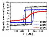
도 2는 종래의 Ta 시드층 이용할 때 CoFeB 자성층의 수직 자화 특성의 그래프이다. 즉, 실리콘 기판 상에 TiN 하부 전극/Ta 시드층/CoFeB 자성층/MgO 터널 배리어 구조를 형성한 후 CoFeB의 수직 자화 특성을 평가하였다. 이때, Ta 시드층은 5㎚, 7㎚ 및 10㎚의 두께로 각각 형성하였고, CoFeB 자성층은 1㎚의 두께로 형성하였으며, MgO 터널 배리어는 2㎚의 두께로 형성하였다. 또한, 300℃, 325℃ 및 350℃의 온도에서 각각 열처리하였다. 도 2에 도시된 바와 같이 CoFeB 자성층은 300℃의 온도에서 높은 수직 자화값을 가질 수 있지만, CoFeB 자성층은 열적 안정성이 낮기 때문에 300℃를 초과하는 온도에서는 CoFeB 자성층의 수직 자화값이 점차 감소하여 350℃에서는 CoFeB 자성층이 보자력(Coercivity)가 감소하고 스퀘어니스(Squareness)가 사라져 수직 자기 특성이 열화되었다.2 is a graph showing the perpendicular magnetization characteristics of a CoFeB magnetic layer when using a conventional Ta seed layer. That is, after the TiN lower electrode / Ta seed layer / CoFeB magnetic layer / MgO tunnel barrier structure was formed on the silicon substrate, the vertical magnetization characteristics of CoFeB were evaluated. At this time, the Ta seed layer was formed to have a thickness of 5 nm, 7 nm and 10 nm, the CoFeB magnetic layer was formed to a thickness of 1 nm, and the MgO tunnel barrier was formed to a thickness of 2 nm. Further, heat treatment was performed at temperatures of 300 캜, 325 캜 and 350 캜, respectively. As shown in FIG. 2, the CoFeB magnetic layer can have a high perpendicular magnetization value at a temperature of 300 ° C., but since the CoFeB magnetic layer has low thermal stability, the perpendicular magnetization value of the CoFeB magnetic layer gradually decreases at a temperature exceeding 300 ° C. The coercivity of CoFeB magnetic layer decreased and squareness disappeared and the perpendicular magnetic properties deteriorated.
도 3은 종래의 Ta 시드층 이용할 때 CoFeAl 자성층의 수직 자화 특성의 그래프이다. 즉, 실리콘 기판 상에 TiN 하부 전극/Ta 시드층/CoFeAl 자성층/MgO 터널 배리어 구조를 형성한 후 CoFeAl의 수직 자화 특성을 평가하였다. 이때, 도 2의 예와 마찬가지로 Ta 시드층은 5㎚, 7㎚ 및 10㎚의 두께로 각각 형성하였고, CoFeAl 자성층은 1㎚의 두께로 형성하였으며, MgO 터널 배리어는 2㎚의 두께로 형성하였다. 도시된 바와 같이 비정질 Ta 시드층은 그 두께가 5㎚∼10㎚로 증가되어도 bcc 결정 특성이 나타나지 않기 때문에 CoFeAl 자성층을 L21 또는 B2 결정 구조로 성장시킬 수 없어 수직 자기 특성이 발현되지 않음을 알 수 있다.3 is a graph of vertical magnetization characteristics of a CoFeAl magnetic layer when using a conventional Ta seed layer. That is, after the TiN lower electrode / Ta seed layer / CoFeAl magnetic layer / MgO tunnel barrier structure was formed on the silicon substrate, the vertical magnetization characteristics of CoFeAl were evaluated. 2, a Ta seed layer was formed to have a thickness of 5 nm, 7 nm, and 10 nm, a CoFeAl magnetic layer was formed to a thickness of 1 nm, and a MgO tunnel barrier was formed to a thickness of 2 nm. As shown in the figure, since the amorphous Ta seed layer does not exhibit the bcc crystal characteristics even when the thickness thereof is increased to 5 nm to 10 nm, the CoFeAl magnetic layer can not be grown to the L21 or B2 crystal structure, have.
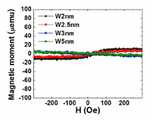
도 4는 Ta 버퍼층과 W 시드층을 이용할 때 CoFeAl 자성층의 수직 자화 특성의 그래프이다. 즉, 실리콘 기판 상에 TiN 하부 전극/Ta 버퍼층/W 시드층/CoFeAl 자성층/MgO 터널 배리어 구조를 형성한 후 CoFeAl의 수직 자화 특성을 평가하였다. 이때, Ta 버퍼층은 5㎚의 두께로 형성하였고, W 시드층은 2㎚, 2.5㎚, 3㎚ 및 5㎚의 두께로 형성하였으며, CoFeAl 자성층은 1㎚의 두께로 형성하였으며, MgO 터널 배리어는 2㎚의 두께로 형성하였다. 도시된 바와 같이 비정질 Ta 버퍼층 위에 bcc 구조의 W 시드층을 2㎚ 내지 5㎚의 두께로 형성하여도 시드층에 bcc 결정 특성이 나타나지 않기 때문에 CoFeAl 자성층을 L21 또는 B2 결정 구조로 성장시킬 수 없어 수직 자기 특성이 발현되지 않음을 알 수 있다.
4 is a graph of vertical magnetization characteristics of a CoFeAl magnetic layer when using a Ta buffer layer and a W seed layer. That is, after the TiN lower electrode / Ta buffer layer / W seed layer / CoFeAl magnetic layer / MgO tunnel barrier structure was formed on the silicon substrate, the vertical magnetization characteristics of CoFeAl were evaluated. At this time, the Ta buffer layer was formed to a thickness of 5 nm, the W seed layer was formed to a thickness of 2 nm, 2.5 nm, 3 nm and 5 nm, the CoFeAl magnetic layer was formed to a thickness of 1 nm, Nm thick. As shown, even if the W seed layer having the bcc structure is formed to a thickness of 2 nm to 5 nm on the amorphous Ta buffer layer, since the bcc crystal characteristic does not appear in the seed layer, the CoFeAl magnetic layer can not be grown into the L21 or B2 crystal structure, It can be seen that the magnetic properties are not expressed.
실시 예Example
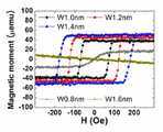
도 5는 본 발명의 실시 예에 따른 Ta 버퍼층과 MgO/W 시드층을 형성한 구조에서 W의 두께에 따른 CoFeAl 자성층의 수직 자화 특성의 그래프이다. 여기서, Ta 버퍼층은 5㎚의 두께로 형성하였고, MgO 시드층은 1.2㎚의 두께로 형성하였으며, W 시드층는 0.8㎚ 내지 1.4㎚의 두께로 형성하였다. 또한, CoFeAl 자성층은 1㎚의 두께로 형성하였고, MgO 터널 배리어는 2㎚의 두께로 형성하였다. MgO층의 두께가 1㎚ 이상이면 자체 bcc 결정화가 이루어지기 때문에 MgO층을 제 1 시드층으로 이용하였다. 이때, MgO 시드층은 1㎚∼1.5㎚로 형성될 수 있으며, 터널 배리어보다 두꺼울 경우 RA 증가로 인해 p-STT MRAM의 중요 요건인 TMR비가 감소된다. MgO 시드층 상에 형성된 W 시드층은 bcc 구조로 형성되며, 1㎚∼1.4㎚일 때 수직 자기 특성이 발현된다. 또한, 종래의 Cr, Ru 시드층과는 달리 별도의 고온 열처리를 통해 bcc 결정화할 필요가 없다. W 시드층 위에 형성된 CoFeAl 자성층은 W bcc 결정 구조를 따라 bcc 결정 구조의 일종인 B2 구조로 형성되었기 때문에 수직 자기 특성이 발현되었다.
5 is a graph showing vertical magnetization characteristics of a CoFeAl magnetic layer according to a thickness of W in a structure in which a Ta buffer layer and an MgO / W seed layer are formed according to an embodiment of the present invention. Here, the Ta buffer layer was formed to a thickness of 5 nm, the MgO seed layer to a thickness of 1.2 nm, and the W seed layer to a thickness of 0.8 to 1.4 nm. The CoFeAl magnetic layer was formed to a thickness of 1 nm, and the MgO tunnel barrier was formed to a thickness of 2 nm. When the thickness of the MgO layer is 1 nm or more, the MgO layer is used as the first seed layer since bcc crystallization is carried out by itself. At this time, the MgO seed layer may be formed at 1 nm to 1.5 nm, and if it is thicker than the tunnel barrier, the TMR ratio, which is an important requirement of the p-STT MRAM, is reduced due to the increase of RA. The W seed layer formed on the MgO seed layer is formed in a bcc structure, and the perpendicular magnetic properties are exhibited when the thickness is 1 nm to 1.4 nm. Further, unlike the conventional Cr and Ru seed layers, it is not necessary to crystallize bcc by a separate high-temperature heat treatment. Since the CoFeAl magnetic layer formed on the W seed layer was formed into a B2 structure, which is a type of bcc crystal structure, along with the W bcc crystal structure, the perpendicular magnetic properties were exhibited.
한편, 본 발명의 기술적 사상은 상기 실시 예에 따라 구체적으로 기술되었으나, 상기 실시 예는 그 설명을 위한 것이며, 그 제한을 위한 것이 아님을 주지해야 한다. 또한, 본 발명의 기술분야에서 당업자는 본 발명의 기술 사상의 범위 내에서 다양한 실시 예가 가능함을 이해할 수 있을 것이다.
While the present invention has been particularly shown and described with reference to exemplary embodiments thereof, it is to be understood that the invention is not limited to the disclosed exemplary embodiments. It will be apparent to those skilled in the art that various modifications and variations can be made in the present invention without departing from the spirit and scope of the invention.
100 : 기판110 : 하부 전극
120 : 버퍼층130 : 시드층
140 : 자유층150 : 터널 배리어
160 : 고정층170 : 캐핑층
180 : 합성 교환 반자성층190 : 상부 전극100: substrate 110: lower electrode
120: buffer layer 130: seed layer
140: free layer 150: tunnel barrier
160: fixed layer 170: capping layer
180: composite exchange-type semi-magnetic layer 190: upper electrode
Claims (12)
Translated fromKorean상기 시드층은 적어도 이중 구조로 형성되며, 적어도 일층이 bcc 구조를 갖는 다결정의 도전 물질로 형성된 메모리 소자.
A lower electrode, a seed layer and a magnetic tunnel junction are laminated on a substrate,
Wherein the seed layer is formed at least of a double structure, and at least one layer is formed of a polycrystalline conductive material having a bcc structure.
The memory element of claim 1, wherein the lower electrode is formed of a polycrystalline conductive material.
The memory device of claim 2, wherein the lower electrode comprises a stacked structure of a first lower electrode including tungsten and a second lower electrode including TiN.
4. The memory device of claim 3, further comprising a buffer layer formed between the lower electrode and the seed layer and formed of a material containing tantalum.
The memory element according to claim 1 or 4, wherein the seed layer is formed by a laminated structure of a first seed layer capable of self-crystallizing at bcc and a second seed layer having a bcc structure.
6. The memory element of claim 5, wherein the first seed layer comprises MgO and the second seed layer comprises W.
7. The memory element according to claim 6, wherein the first seed layer is formed to be thinner than the tunnel barrier of the magnetic tunnel junction.
The memory element according to claim 7, wherein the first seed layer is formed to a thickness of 1 nm to 1.5 nm, and the second seed layer is formed to a thickness of 1 nm to 1.4 nm.
The memory element according to claim 7, wherein the magnetic layer of the magnetic tunnel junction comprises at least one of CoFeAl and CoFeAlSi.
The memory device of claim 5, further comprising a capping layer formed over the magnetic tunnel junction, a synthetic exchange ferromagnetic layer and an upper electrode,
11. The memory element of claim 10, wherein the capping layer is formed of a material comprising at least one of tantalum and tungsten.
Applications Claiming Priority (4)
| Application Number | Priority Date | Filing Date | Title |
|---|---|---|---|
| KR1020140046563 | 2014-04-18 | ||
| KR1020140046563 | 2014-04-18 | ||
| KR20150037230 | 2015-03-18 | ||
| KR1020150037230 | 2015-03-18 |
Publications (2)
| Publication Number | Publication Date |
|---|---|
| KR20150120857A KR20150120857A (en) | 2015-10-28 |
| KR101661275B1true KR101661275B1 (en) | 2016-09-29 |
Family
ID=56918927
Family Applications (1)
| Application Number | Title | Priority Date | Filing Date |
|---|---|---|---|
| KR1020150045170AExpired - Fee RelatedKR101661275B1 (en) | 2014-04-18 | 2015-03-31 | Memory device |
Country Status (3)
| Country | Link |
|---|---|
| KR (1) | KR101661275B1 (en) |
| CN (1) | CN107534081B (en) |
| WO (1) | WO2016148391A1 (en) |
Families Citing this family (9)
| Publication number | Priority date | Publication date | Assignee | Title |
|---|---|---|---|---|
| CN109155360A (en) | 2016-02-05 | 2019-01-04 | 汉阳大学校产学协力团 | memory device |
| CN107452869A (en)* | 2016-05-31 | 2017-12-08 | 上海磁宇信息科技有限公司 | A kind of vertical-type magnetoresistive element and its manufacturing process |
| KR20180095147A (en) | 2017-02-16 | 2018-08-27 | 에스케이하이닉스 주식회사 | Electronic device and method for fabricating the same |
| CN110098318B (en)* | 2019-05-10 | 2020-11-03 | 北京航空航天大学 | Multi-film layer structure with interface perpendicular magnetic anisotropy and magnetic random access memory |
| CN112490352B (en)* | 2019-09-11 | 2023-10-27 | 上海磁宇信息科技有限公司 | Magnetic tunnel junction structure of magnetic random access memory |
| CN113451504B (en)* | 2020-03-24 | 2023-03-24 | 上海磁宇信息科技有限公司 | Magnetic random access memory cell with composite seed layer structure |
| CN111509120A (en)* | 2020-04-21 | 2020-08-07 | 浙江驰拓科技有限公司 | Magnetic tunnel junction and method of manufacturing the same |
| US12274179B2 (en) | 2022-06-17 | 2025-04-08 | International Business Machines Corporation | Seed layer for enhancing tunnel magnetoresistance with perpendicularly magnetized Heusler films |
| US20240155950A1 (en) | 2022-11-07 | 2024-05-09 | International Business Machines Corporation | Seed layer for enhancing tunnel magnetoresistance with perpendicularly magnetized heusler films |
Family Cites Families (17)
| Publication number | Priority date | Publication date | Assignee | Title |
|---|---|---|---|---|
| KR100278786B1 (en)* | 1998-06-18 | 2001-01-15 | 구자홍 | Optical Recording Medium and Optical Recording/Reproducing Method and Apparatus |
| US6429497B1 (en)* | 2000-11-18 | 2002-08-06 | Hewlett-Packard Company | Method for improving breakdown voltage in magnetic tunnel junctions |
| US6649423B2 (en)* | 2001-10-04 | 2003-11-18 | Hewlett-Packard Development Company, L.P. | Method for modifying switching field characteristics of magnetic tunnel junctions |
| US7141272B2 (en)* | 2004-02-02 | 2006-11-28 | Fujitsu Limited | Method of producing magnetic recording medium |
| JP2005251373A (en)* | 2004-02-02 | 2005-09-15 | Fujitsu Ltd | Magnetic recording medium, manufacturing method thereof, and magnetic storage device |
| US8057925B2 (en)* | 2008-03-27 | 2011-11-15 | Magic Technologies, Inc. | Low switching current dual spin filter (DSF) element for STT-RAM and a method for making the same |
| WO2010026667A1 (en)* | 2008-09-03 | 2010-03-11 | Canon Anelva Corporation | Ferromagnetic preferred grain growth promotion seed layer for amorphous or microcrystalline mgo tunnel barrier |
| JP5534766B2 (en)* | 2009-06-19 | 2014-07-02 | Tdk株式会社 | Spin valve structure of spintronic element and method for forming the same, bottom type spin valve structure, and spintronic element for microwave assisted magnetic recording |
| EP2360291A1 (en)* | 2010-02-24 | 2011-08-24 | Singulus Technologies AG | Method and device for quick heating and cooling of a substrate and immediately coating same in a vacuum |
| KR101849677B1 (en)* | 2011-05-19 | 2018-04-19 | 삼성전자주식회사 | Magnetic Tunnel Junction Element |
| US8710602B2 (en)* | 2011-12-20 | 2014-04-29 | Samsung Electronics Co., Ltd. | Method and system for providing magnetic junctions having improved characteristics |
| KR101446338B1 (en)* | 2012-07-17 | 2014-10-01 | 삼성전자주식회사 | Magnetic device and method of manufacturing the same |
| KR20140025165A (en)* | 2012-08-21 | 2014-03-04 | 삼성전자주식회사 | Method of fabricating a magnetic memory device |
| JP6083163B2 (en)* | 2012-09-11 | 2017-02-22 | 富士電機株式会社 | Perpendicular magnetic recording medium and manufacturing method thereof |
| KR102082328B1 (en)* | 2013-07-03 | 2020-02-27 | 삼성전자주식회사 | Magnetic memory devices having perpendicular magnetic tunnel junction |
| KR101636492B1 (en)* | 2013-07-31 | 2016-07-20 | 한양대학교 산학협력단 | Memory device |
| KR20150015602A (en)* | 2013-07-31 | 2015-02-11 | 한양대학교 산학협력단 | Memory device |
- 2015
- 2015-03-31KRKR1020150045170Apatent/KR101661275B1/ennot_activeExpired - Fee Related
- 2016
- 2016-02-02WOPCT/KR2016/001124patent/WO2016148391A1/ennot_activeCeased
- 2016-02-02CNCN201680016553.3Apatent/CN107534081B/ennot_activeExpired - Fee Related
Also Published As
| Publication number | Publication date |
|---|---|
| WO2016148391A1 (en) | 2016-09-22 |
| KR20150120857A (en) | 2015-10-28 |
| CN107534081B (en) | 2020-12-01 |
| CN107534081A (en) | 2018-01-02 |
Similar Documents
| Publication | Publication Date | Title |
|---|---|---|
| US10783945B2 (en) | Memory device | |
| US10580964B2 (en) | Memory device | |
| KR101661275B1 (en) | Memory device | |
| KR101549625B1 (en) | Memory device | |
| KR20190087943A (en) | Memory device | |
| KR20150015602A (en) | Memory device | |
| KR101721618B1 (en) | Memory device | |
| KR101636492B1 (en) | Memory device | |
| KR101537715B1 (en) | Memory device | |
| KR101705125B1 (en) | Memory device | |
| KR101956975B1 (en) | Memory device | |
| KR101698532B1 (en) | Memory device | |
| KR101583783B1 (en) | Memory device | |
| KR101756883B1 (en) | Memory device | |
| WO2016148392A1 (en) | Memory device | |
| KR101956976B1 (en) | Memory device | |
| KR101933268B1 (en) | Memory device | |
| KR101956977B1 (en) | Memory device | |
| WO2016148395A1 (en) | Memory device | |
| WO2016148393A1 (en) | Memory device |
Legal Events
| Date | Code | Title | Description |
|---|---|---|---|
| A201 | Request for examination | ||
| PA0109 | Patent application | St.27 status event code:A-0-1-A10-A12-nap-PA0109 | |
| PA0201 | Request for examination | St.27 status event code:A-1-2-D10-D11-exm-PA0201 | |
| PG1501 | Laying open of application | St.27 status event code:A-1-1-Q10-Q12-nap-PG1501 | |
| E701 | Decision to grant or registration of patent right | ||
| PE0701 | Decision of registration | St.27 status event code:A-1-2-D10-D22-exm-PE0701 | |
| GRNT | Written decision to grant | ||
| PR0701 | Registration of establishment | St.27 status event code:A-2-4-F10-F11-exm-PR0701 | |
| PR1002 | Payment of registration fee | St.27 status event code:A-2-2-U10-U11-oth-PR1002 Fee payment year number:1 | |
| PG1601 | Publication of registration | St.27 status event code:A-4-4-Q10-Q13-nap-PG1601 | |
| P22-X000 | Classification modified | St.27 status event code:A-4-4-P10-P22-nap-X000 | |
| FPAY | Annual fee payment | Payment date:20190624 Year of fee payment:4 | |
| PR1001 | Payment of annual fee | St.27 status event code:A-4-4-U10-U11-oth-PR1001 Fee payment year number:4 | |
| R18-X000 | Changes to party contact information recorded | St.27 status event code:A-5-5-R10-R18-oth-X000 | |
| R18-X000 | Changes to party contact information recorded | St.27 status event code:A-5-5-R10-R18-oth-X000 | |
| PR1001 | Payment of annual fee | St.27 status event code:A-4-4-U10-U11-oth-PR1001 Fee payment year number:5 | |
| PR1001 | Payment of annual fee | St.27 status event code:A-4-4-U10-U11-oth-PR1001 Fee payment year number:6 | |
| PC1903 | Unpaid annual fee | St.27 status event code:A-4-4-U10-U13-oth-PC1903 Not in force date:20220924 Payment event data comment text:Termination Category : DEFAULT_OF_REGISTRATION_FEE | |
| P22-X000 | Classification modified | St.27 status event code:A-4-4-P10-P22-nap-X000 | |
| P22-X000 | Classification modified | St.27 status event code:A-4-4-P10-P22-nap-X000 | |
| PC1903 | Unpaid annual fee | St.27 status event code:N-4-6-H10-H13-oth-PC1903 Ip right cessation event data comment text:Termination Category : DEFAULT_OF_REGISTRATION_FEE Not in force date:20220924 | |
| P22-X000 | Classification modified | St.27 status event code:A-4-4-P10-P22-nap-X000 |