KR101657872B1 - Improved transistor channel - Google Patents
Improved transistor channelDownload PDFInfo
- Publication number
- KR101657872B1 KR101657872B1KR1020150012709AKR20150012709AKR101657872B1KR 101657872 B1KR101657872 B1KR 101657872B1KR 1020150012709 AKR1020150012709 AKR 1020150012709AKR 20150012709 AKR20150012709 AKR 20150012709AKR 101657872 B1KR101657872 B1KR 101657872B1
- Authority
- KR
- South Korea
- Prior art keywords
- source
- transistor
- semiconductor material
- region
- semiconductor
- Prior art date
- Legal status (The legal status is an assumption and is not a legal conclusion. Google has not performed a legal analysis and makes no representation as to the accuracy of the status listed.)
- Active
Links
- 239000004065semiconductorSubstances0.000claimsabstractdescription133
- 239000000463materialSubstances0.000claimsabstractdescription110
- 239000000758substrateSubstances0.000claimsabstractdescription48
- 238000000034methodMethods0.000claimsdescription107
- 229910000577Silicon-germaniumInorganic materials0.000claimsdescription23
- LEVVHYCKPQWKOP-UHFFFAOYSA-N[Si].[Ge]Chemical compound[Si].[Ge]LEVVHYCKPQWKOP-UHFFFAOYSA-N0.000claimsdescription17
- 239000002019doping agentSubstances0.000claimsdescription12
- ZOXJGFHDIHLPTG-UHFFFAOYSA-NBoronChemical compound[B]ZOXJGFHDIHLPTG-UHFFFAOYSA-N0.000claimsdescription8
- 229910052796boronInorganic materials0.000claimsdescription8
- 238000000059patterningMethods0.000claimsdescription8
- OAICVXFJPJFONN-UHFFFAOYSA-NPhosphorusChemical compound[P]OAICVXFJPJFONN-UHFFFAOYSA-N0.000claimsdescription6
- 229910052698phosphorusInorganic materials0.000claimsdescription6
- 239000011574phosphorusSubstances0.000claimsdescription6
- 229910000530Gallium indium arsenideInorganic materials0.000claimsdescription5
- KXNLCSXBJCPWGL-UHFFFAOYSA-N[Ga].[As].[In]Chemical compound[Ga].[As].[In]KXNLCSXBJCPWGL-UHFFFAOYSA-N0.000claimsdescription5
- 239000010410layerSubstances0.000description69
- 235000012431wafersNutrition0.000description26
- 238000005530etchingMethods0.000description13
- 229910052710siliconInorganic materials0.000description11
- XUIMIQQOPSSXEZ-UHFFFAOYSA-NSiliconChemical compound[Si]XUIMIQQOPSSXEZ-UHFFFAOYSA-N0.000description10
- 239000003989dielectric materialSubstances0.000description10
- 239000007789gasSubstances0.000description10
- 239000010703siliconSubstances0.000description10
- 238000005229chemical vapour depositionMethods0.000description8
- 238000004519manufacturing processMethods0.000description8
- 238000000231atomic layer depositionMethods0.000description7
- VYPSYNLAJGMNEJ-UHFFFAOYSA-NSilicium dioxideChemical compoundO=[Si]=OVYPSYNLAJGMNEJ-UHFFFAOYSA-N0.000description6
- 238000000151depositionMethods0.000description6
- 238000010586diagramMethods0.000description6
- 238000002955isolationMethods0.000description6
- 238000004518low pressure chemical vapour depositionMethods0.000description6
- 229910052814silicon oxideInorganic materials0.000description6
- 125000006850spacer groupChemical group0.000description6
- WGTYBPLFGIVFAS-UHFFFAOYSA-Mtetramethylammonium hydroxideChemical compound[OH-].C[N+](C)(C)CWGTYBPLFGIVFAS-UHFFFAOYSA-M0.000description6
- 229910052581Si3N4Inorganic materials0.000description5
- 230000015572biosynthetic processEffects0.000description5
- 238000001312dry etchingMethods0.000description5
- 238000005240physical vapour depositionMethods0.000description5
- HQVNEWCFYHHQES-UHFFFAOYSA-Nsilicon nitrideChemical compoundN12[Si]34N5[Si]62N3[Si]51N64HQVNEWCFYHHQES-UHFFFAOYSA-N0.000description5
- VEXZGXHMUGYJMC-UHFFFAOYSA-NHydrochloric acidChemical compoundClVEXZGXHMUGYJMC-UHFFFAOYSA-N0.000description4
- 238000000137annealingMethods0.000description4
- 239000000460chlorineSubstances0.000description4
- 239000012212insulatorSubstances0.000description4
- 229920002120photoresistant polymerPolymers0.000description4
- JBRZTFJDHDCESZ-UHFFFAOYSA-NAsGaChemical compound[As]#[Ga]JBRZTFJDHDCESZ-UHFFFAOYSA-N0.000description3
- ZAMOUSCENKQFHK-UHFFFAOYSA-NChlorine atomChemical compound[Cl]ZAMOUSCENKQFHK-UHFFFAOYSA-N0.000description3
- GPXJNWSHGFTCBW-UHFFFAOYSA-NIndium phosphideChemical compound[In]#PGPXJNWSHGFTCBW-UHFFFAOYSA-N0.000description3
- 230000008901benefitEffects0.000description3
- 229910052801chlorineInorganic materials0.000description3
- 238000005137deposition processMethods0.000description3
- 229910052732germaniumInorganic materials0.000description3
- GNPVGFCGXDBREM-UHFFFAOYSA-Ngermanium atomChemical compound[Ge]GNPVGFCGXDBREM-UHFFFAOYSA-N0.000description3
- 229910052751metalInorganic materials0.000description3
- 239000002184metalSubstances0.000description3
- 239000000203mixtureSubstances0.000description3
- HBMJWWWQQXIZIP-UHFFFAOYSA-Nsilicon carbideChemical compound[Si+]#[C-]HBMJWWWQQXIZIP-UHFFFAOYSA-N0.000description3
- 229910010271silicon carbideInorganic materials0.000description3
- 230000005641tunnelingEffects0.000description3
- 238000001039wet etchingMethods0.000description3
- 229910018072Al 2 O 3Inorganic materials0.000description2
- XKRFYHLGVUSROY-UHFFFAOYSA-NArgonChemical compound[Ar]XKRFYHLGVUSROY-UHFFFAOYSA-N0.000description2
- IJGRMHOSHXDMSA-UHFFFAOYSA-NAtomic nitrogenChemical compoundN#NIJGRMHOSHXDMSA-UHFFFAOYSA-N0.000description2
- RYGMFSIKBFXOCR-UHFFFAOYSA-NCopperChemical compound[Cu]RYGMFSIKBFXOCR-UHFFFAOYSA-N0.000description2
- 229910001218Gallium arsenideInorganic materials0.000description2
- 229910045601alloyInorganic materials0.000description2
- 239000000956alloySubstances0.000description2
- FTWRSWRBSVXQPI-UHFFFAOYSA-Nalumanylidynearsane;gallanylidynearsaneChemical compound[As]#[Al].[As]#[Ga]FTWRSWRBSVXQPI-UHFFFAOYSA-N0.000description2
- 230000004888barrier functionEffects0.000description2
- 239000011248coating agentSubstances0.000description2
- 238000000576coating methodMethods0.000description2
- 230000000295complement effectEffects0.000description2
- 150000001875compoundsChemical class0.000description2
- 229910052802copperInorganic materials0.000description2
- 239000010949copperSubstances0.000description2
- 230000005669field effectEffects0.000description2
- 239000007943implantSubstances0.000description2
- 238000011065in-situ storageMethods0.000description2
- 229910044991metal oxideInorganic materials0.000description2
- 150000004706metal oxidesChemical class0.000description2
- 230000003647oxidationEffects0.000description2
- 238000007254oxidation reactionMethods0.000description2
- TWNQGVIAIRXVLR-UHFFFAOYSA-Noxo(oxoalumanyloxy)alumaneChemical compoundO=[Al]O[Al]=OTWNQGVIAIRXVLR-UHFFFAOYSA-N0.000description2
- 229910021420polycrystalline siliconInorganic materials0.000description2
- 229920005591polysiliconPolymers0.000description2
- 239000002243precursorSubstances0.000description2
- 238000004151rapid thermal annealingMethods0.000description2
- 229910021332silicideInorganic materials0.000description2
- FVBUAEGBCNSCDD-UHFFFAOYSA-Nsilicide(4-)Chemical compound[Si-4]FVBUAEGBCNSCDD-UHFFFAOYSA-N0.000description2
- WFKWXMTUELFFGS-UHFFFAOYSA-NtungstenChemical compound[W]WFKWXMTUELFFGS-UHFFFAOYSA-N0.000description2
- 229910052721tungstenInorganic materials0.000description2
- 239000010937tungstenSubstances0.000description2
- 238000000038ultrahigh vacuum chemical vapour depositionMethods0.000description2
- 238000000927vapour-phase epitaxyMethods0.000description2
- ITWBWJFEJCHKSN-UHFFFAOYSA-N1,4,7-triazonaneChemical compoundC1CNCCNCCN1ITWBWJFEJCHKSN-UHFFFAOYSA-N0.000description1
- ZCYVEMRRCGMTRW-UHFFFAOYSA-N7553-56-2Chemical compound[I]ZCYVEMRRCGMTRW-UHFFFAOYSA-N0.000description1
- WKBOTKDWSSQWDR-UHFFFAOYSA-NBromine atomChemical compound[Br]WKBOTKDWSSQWDR-UHFFFAOYSA-N0.000description1
- OKTJSMMVPCPJKN-UHFFFAOYSA-NCarbonChemical compound[C]OKTJSMMVPCPJKN-UHFFFAOYSA-N0.000description1
- 229910005540GaPInorganic materials0.000description1
- 229910004129HfSiOInorganic materials0.000description1
- ZOKXTWBITQBERF-UHFFFAOYSA-NMolybdenumChemical compound[Mo]ZOKXTWBITQBERF-UHFFFAOYSA-N0.000description1
- 229920001218PullulanPolymers0.000description1
- 229910004200TaSiNInorganic materials0.000description1
- 229910010038TiAlInorganic materials0.000description1
- 229910010037TiAlNInorganic materials0.000description1
- ATJFFYVFTNAWJD-UHFFFAOYSA-NTinChemical compound[Sn]ATJFFYVFTNAWJD-UHFFFAOYSA-N0.000description1
- RTAQQCXQSZGOHL-UHFFFAOYSA-NTitaniumChemical compound[Ti]RTAQQCXQSZGOHL-UHFFFAOYSA-N0.000description1
- 229910052782aluminiumInorganic materials0.000description1
- XAGFODPZIPBFFR-UHFFFAOYSA-NaluminiumChemical compound[Al]XAGFODPZIPBFFR-UHFFFAOYSA-N0.000description1
- PNEYBMLMFCGWSK-UHFFFAOYSA-Naluminium oxideInorganic materials[O-2].[O-2].[O-2].[Al+3].[Al+3]PNEYBMLMFCGWSK-UHFFFAOYSA-N0.000description1
- 229910052786argonInorganic materials0.000description1
- 229910052785arsenicInorganic materials0.000description1
- RQNWIZPPADIBDY-UHFFFAOYSA-Narsenic atomChemical compound[As]RQNWIZPPADIBDY-UHFFFAOYSA-N0.000description1
- QVGXLLKOCUKJST-UHFFFAOYSA-Natomic oxygenChemical compound[O]QVGXLLKOCUKJST-UHFFFAOYSA-N0.000description1
- GDTBXPJZTBHREO-UHFFFAOYSA-NbromineSubstancesBrBrGDTBXPJZTBHREO-UHFFFAOYSA-N0.000description1
- 229910052794bromiumInorganic materials0.000description1
- 229910052799carbonInorganic materials0.000description1
- 239000010941cobaltSubstances0.000description1
- 229910017052cobaltInorganic materials0.000description1
- GUTLYIVDDKVIGB-UHFFFAOYSA-Ncobalt atomChemical compound[Co]GUTLYIVDDKVIGB-UHFFFAOYSA-N0.000description1
- 239000004020conductorSubstances0.000description1
- 238000010276constructionMethods0.000description1
- 230000003247decreasing effectEffects0.000description1
- 230000008021depositionEffects0.000description1
- 238000009792diffusion processMethods0.000description1
- 230000009977dual effectEffects0.000description1
- 238000000407epitaxyMethods0.000description1
- HZXMRANICFIONG-UHFFFAOYSA-Ngallium phosphideChemical compound[Ga]#PHZXMRANICFIONG-UHFFFAOYSA-N0.000description1
- 229910052735hafniumInorganic materials0.000description1
- VBJZVLUMGGDVMO-UHFFFAOYSA-Nhafnium atomChemical compound[Hf]VBJZVLUMGGDVMO-UHFFFAOYSA-N0.000description1
- 238000002513implantationMethods0.000description1
- WPYVAWXEWQSOGY-UHFFFAOYSA-Nindium antimonideChemical compound[Sb]#[In]WPYVAWXEWQSOGY-UHFFFAOYSA-N0.000description1
- 239000011229interlayerSubstances0.000description1
- 229910052740iodineInorganic materials0.000description1
- 239000011630iodineSubstances0.000description1
- 238000005468ion implantationMethods0.000description1
- 238000005224laser annealingMethods0.000description1
- 238000001451molecular beam epitaxyMethods0.000description1
- 229910052750molybdenumInorganic materials0.000description1
- 239000011733molybdenumSubstances0.000description1
- 125000000896monocarboxylic acid groupChemical group0.000description1
- RUFLMLWJRZAWLJ-UHFFFAOYSA-Nnickel silicideChemical compound[Ni]=[Si]=[Ni]RUFLMLWJRZAWLJ-UHFFFAOYSA-N0.000description1
- 229910021334nickel silicideInorganic materials0.000description1
- 229910052757nitrogenInorganic materials0.000description1
- 239000001301oxygenSubstances0.000description1
- 229910052760oxygenInorganic materials0.000description1
- RVTZCBVAJQQJTK-UHFFFAOYSA-Noxygen(2-);zirconium(4+)Chemical compound[O-2].[O-2].[Zr+4]RVTZCBVAJQQJTK-UHFFFAOYSA-N0.000description1
- 238000002161passivationMethods0.000description1
- 235000019423pullulanNutrition0.000description1
- 238000000926separation methodMethods0.000description1
- 239000000126substanceSubstances0.000description1
- 238000006467substitution reactionMethods0.000description1
- 229910052715tantalumInorganic materials0.000description1
- GUVRBAGPIYLISA-UHFFFAOYSA-Ntantalum atomChemical compound[Ta]GUVRBAGPIYLISA-UHFFFAOYSA-N0.000description1
- MZLGASXMSKOWSE-UHFFFAOYSA-Ntantalum nitrideChemical compound[Ta]#NMZLGASXMSKOWSE-UHFFFAOYSA-N0.000description1
- 239000010936titaniumSubstances0.000description1
- 229910052719titaniumInorganic materials0.000description1
- 229910001928zirconium oxideInorganic materials0.000description1
Images


Classifications
- H01L29/7855—
- H—ELECTRICITY
- H10—SEMICONDUCTOR DEVICES; ELECTRIC SOLID-STATE DEVICES NOT OTHERWISE PROVIDED FOR
- H10D—INORGANIC ELECTRIC SEMICONDUCTOR DEVICES
- H10D30/00—Field-effect transistors [FET]
- H10D30/60—Insulated-gate field-effect transistors [IGFET]
- H10D30/62—Fin field-effect transistors [FinFET]
- H—ELECTRICITY
- H10—SEMICONDUCTOR DEVICES; ELECTRIC SOLID-STATE DEVICES NOT OTHERWISE PROVIDED FOR
- H10D—INORGANIC ELECTRIC SEMICONDUCTOR DEVICES
- H10D64/00—Electrodes of devices having potential barriers
- H10D64/01—Manufacture or treatment
- H10D64/017—Manufacture or treatment using dummy gates in processes wherein at least parts of the final gates are self-aligned to the dummy gates, i.e. replacement gate processes
- H01L29/7848—
- H—ELECTRICITY
- H10—SEMICONDUCTOR DEVICES; ELECTRIC SOLID-STATE DEVICES NOT OTHERWISE PROVIDED FOR
- H10D—INORGANIC ELECTRIC SEMICONDUCTOR DEVICES
- H10D30/00—Field-effect transistors [FET]
- H10D30/01—Manufacture or treatment
- H10D30/021—Manufacture or treatment of FETs having insulated gates [IGFET]
- H10D30/024—Manufacture or treatment of FETs having insulated gates [IGFET] of fin field-effect transistors [FinFET]
- H—ELECTRICITY
- H10—SEMICONDUCTOR DEVICES; ELECTRIC SOLID-STATE DEVICES NOT OTHERWISE PROVIDED FOR
- H10D—INORGANIC ELECTRIC SEMICONDUCTOR DEVICES
- H10D62/00—Semiconductor bodies, or regions thereof, of devices having potential barriers
- H10D62/10—Shapes, relative sizes or dispositions of the regions of the semiconductor bodies; Shapes of the semiconductor bodies
- H10D62/13—Semiconductor regions connected to electrodes carrying current to be rectified, amplified or switched, e.g. source or drain regions
- H10D62/149—Source or drain regions of field-effect devices
- H10D62/151—Source or drain regions of field-effect devices of IGFETs
Landscapes
- Insulated Gate Type Field-Effect Transistor (AREA)
- Metal-Oxide And Bipolar Metal-Oxide Semiconductor Integrated Circuits (AREA)
Abstract
Description
Translated fromKorean본 발명은 반도체 디바이스에 관한 것이다.The present invention relates to a semiconductor device.
반도체 집적 회로(IC) 산업은 지난 수십년간 급속한 성장을 이루었다. 반도체 물질 및 설계에서의 기술적인 발전은 점점 더 작고 더욱 복잡한 회로를 생산했다. 처리 및 제조에 과련된 기술들이 또한 기술적 발전을 겪었기 때문에 이러한 물질 및 설계의 발전이 가능하게 되었다. 가장 작은 컴포넌트의 크기가 감소됨에 따라, 다양한 도전 과제들이 증가했다. 예를 들어, 핀 전계 효과 트랜지스터(fin-like field-effect transistor; FinFET)와 같은 3 차원 트랜지스터가 도입되었다. 기존의 디바이스 및 디바이스를 제조하는 방법은 일반적으로 자신의 의도된 목적에는 적절하지만, 모든 면에서 완전히 만족스러운 것은 아니다. 예를 들어, 유효 게이트 길이의 제한은 FinFET를 비록한, 반도체 디바이스 개발에 도전 과제들을 발생시킨다. 이 영역을 개선하는 것이 바람직하다.The semiconductor integrated circuit (IC) industry has experienced rapid growth over the past several decades. Technological advances in semiconductor materials and design have produced smaller and more complex circuits. Technological advances in processing and manufacturing have also undergone technological advancement, enabling the development of such materials and designs. As the size of the smallest component is reduced, various challenges have increased. For example, a three-dimensional transistor such as a fin-like field-effect transistor (FinFET) has been introduced. Methods of fabricating existing devices and devices are generally appropriate for their intended purposes, but are not entirely satisfactory in all respects. For example, limiting the effective gate length creates challenges for semiconductor device development, even for FinFETs. It is desirable to improve this area.
본 발명의 목적은 개선된 트랜지스터 채널을 제공하는 것이다.It is an object of the present invention to provide an improved transistor channel.
일례에 따라, 트랜지스터 디바이스는 제 1 영역 및 제 2 영역을 갖는 기판, 제 1 영역 위의 제 1 부분 및 제 2 영역 위의 제 2 부분을 갖는 제 1 반도체 물질의 제 1 반도체층을 포함하고, 제 1 부분은 제 2 부분과 분리된다. 디바이스는 제 1 반도체층의 제 2 분분 위의 제 2 반도체 물질의 제 2 반도체층, 제 1 전도성 유형의 제 1 트랜지스터, 및 제 2 전도성 유형의 제 2 트랜지스터를 더 포함하고, 제 1 트랜지스터는 제 1 반도체층에 형성된 제 1 세트의 소스/드레인 영역을 갖고 제 1 영역 내에 배치되며, 제 2 트랜지스터는 제 2 반도체층에 형성된 제 2 세트의 소스/드레인 영역을 갖고 제 2 영역 내에 배치된다. 제 1 전도성 유형은 제 2 전도성 유형과 상이하고, 제 2 반도체 물질은 제 1 반도체 물질과 상이하다.According to one example, a transistor device comprises a substrate having a first region and a second region, a first semiconductor layer of a first semiconductor material having a first portion over the first region and a second portion over the second region, The first part is separated from the second part. The device further comprises a second semiconductor layer of a second semiconductor material on a second portion of the first semiconductor layer, a first transistor of a first conductivity type, and a second transistor of a second conductivity type, Drain region and a second set of source / drain regions formed in the second semiconductor layer, and the second transistor is disposed in the second region. The first conductivity type is different from the second conductivity type, and the second semiconductor material is different from the first semiconductor material.
일례에 따라, 트랜지스터 디바이스는 게이트 디바이스, 게이트 디바이스 아래의 채널 쪽을 향하는 꼭짓점을 갖는 소스 영역, 및 채널 쪽을 향하는 꼭짓점을 갖는 드레인 영역을 포함한다. 소스 영역의 꼭짓점에서의 팁 및 드레인 영역의 꼭짓점에서의 팁은 초격자 구조물을 포함한다.According to one example, a transistor device includes a gate device, a source region having a vertex pointing towards the channel under the gate device, and a drain region having a vertex toward the channel. The tip at the apex of the tip and drain regions at the apex of the source region includes a superlattice structure.
일례에 따라, 반도체 디바이스를 제조하기 위한 방법은, 기판 및 제 1 반도체 물질층을 포함하는 제 1 웨이퍼를 제공하는 단계, 제 1 웨이퍼를 제 2 웨이퍼에 본딩하는 단계로서, 제 2 웨이퍼는 희생층 및 제 2 반도체 물질층을 포함하는 것인, 본딩 단계, 희생층을 제거하는 단계, 제 1 구조물 및 제 2 구조물을 생성하기 위해 본딩된 웨이퍼를 패턴화하는 단계, 제 1 구조물로부터 제 2 반도체 물질을 제거하는 단계, 제 1 구조물의 제 1 반도체 물질에 제 1 유형의 트랜지스터를 형성하는 단계, 및 제 2 구조물의 제 2 반도체 물질에 제 2 유형의 트랜지스터를 형성하는 단계를 포함한다.According to one example, a method for manufacturing a semiconductor device includes providing a first wafer comprising a substrate and a first layer of semiconductor material, bonding a first wafer to a second wafer, And removing the sacrificial layer, patterning the bonded wafer to produce a first structure and a second structure, depositing a second semiconductor material from the first structure, Forming a first type of transistor in the first semiconductor material of the first structure, and forming a second type of transistor in the second semiconductor material of the second structure.
본 발명에 따르면, 개선된 트랜지스터 채널을 제공하는 것이 가능하다.According to the present invention, it is possible to provide an improved transistor channel.
본 발명개시의 양태는 첨부 도면들과 함께 아래의 상세한 설명을 읽음으로써 가장 잘 이해된다. 본 산업계에서의 표준적인 실시에 따라, 다양한 피처(feature)들은 실척도로 도시되지 않았음을 유념한다. 사실, 다양한 피처들의 치수는 설명의 명료함을 위해 임의적으로 증가되거나 또는 감소될 수 있다.
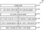
도 1은 본 명세서에 기술된 원리들의 일례에 따라, 반도체 디바이스를 제조하기 위한 예시적인 방법을 도시하는 흐름도이다.
도 2 내지 도 6은 본 명세서에 기술된 원리들의 일례에 따라, 도 1의 방법에 기술된 제조 단계들에서의 예시적인 반도체 디바이스의 횡단면도를 나타낸다.
도 7a 내지 도 7h는 본 명세서에 기술된 원리들의 일례에 따라, 트랜지스터 디바이스에 임베디드 채널을 형성하기 위한 예시적인 공정을 도시하는 도면이다.
도 8은 본 명세서에 기술된 원리들의 일례에 따라, 높은 도펀트 농도를 갖는 예시적인 팁(tip)을 도시하는 도면이다.
도 9는 본 명세서에 기술된 원리들의 일례에 따라, 초격자 구조물을 갖는 예시적인 팁을 도시하는 도면이다.
도 10은 본 명세서에 기술된 원리들의 일례에 따라, 개선된 채널을 갖는 트랜지스터를 형성하는 예시적인 방법을 도시하는 흐름도이다.Embodiments of the present disclosure are best understood by reading the following detailed description together with the accompanying drawings. Note that according to standard practice in the industry, various features are not shown in scale. In fact, the dimensions of the various features may be increased or decreased arbitrarily for clarity of explanation.
1 is a flow chart illustrating an exemplary method for manufacturing a semiconductor device, in accordance with one example of the principles described herein.
Figures 2-6 illustrate a cross-sectional view of an exemplary semiconductor device in the fabrication steps described in the method of Figure 1, in accordance with an example of the principles described herein.
7A-7H illustrate an exemplary process for forming an embedded channel in a transistor device, in accordance with one example of the principles described herein.
8 is a diagram illustrating an exemplary tip having a high dopant concentration, in accordance with one example of the principles described herein.
Figure 9 is a diagram illustrating an exemplary tip with a superlattice structure, in accordance with an example of the principles described herein.
10 is a flow diagram illustrating an exemplary method of forming a transistor having an improved channel, in accordance with one example of the principles described herein.
다음의 발명개시는 제공된 주제의 상이한 피처들을 구현하는 다수의 상이한 실시예들, 또는 예들을 제공한다. 컴포넌트 및 배치의 특정한 예들은 본 발명개시를 단순화하기 위해 이하에 설명된다. 물론, 이러한 설명은 단지 예일 뿐 제한하기 위한 것이 아니다. 예를 들어, 이어지는 설명에서 제 2 피처 위에 또는 제 2 피처 상에 제 1 피처의 형성은, 제 1 피처 및 제 2 피처가 직접 접촉하여 형성되는 실시예들을 포함할 수 있고, 제 1 피처 및 제 2 피처가 직접 접촉하지 않도록 제 1 피처와 제 2 피처 사이에 부가적인 피처들이 형성되는 실시예들을 또한 포함할 수 있다. 게다가, 본 발명개시는 다양한 예들에서 참조 번호 및/또는 문자를 반복할 수 있다. 이러한 반복은 단순함과 명료함을 위한 것으로, 그 자체가 논의된 다양한 실시예들 및/또는 구성들 사이의 관계를 지시하지 않는다.The following inventive disclosures provide a number of different embodiments, or examples, that implement different features of a given subject matter. Specific examples of components and arrangements are described below to simplify disclosure of the present invention. Of course, this description is for illustrative purposes only, and not for limitation. For example, in the following description, formation of a first feature on a second feature or on a second feature may include embodiments in which a first feature and a second feature are formed in direct contact, and the first feature and the second feature 2 features may be formed between the first feature and the second feature such that the second feature is not in direct contact. In addition, the disclosure of the present invention may repeat the reference numerals and / or characters in various examples. Such repetition is for simplicity and clarity and does not itself dictate the relationship between the various embodiments and / or configurations discussed.
더욱이, "아래", "밑", "하위", "위", "상위" 등과 같은 공간적 관계 용어들이 도면들에 나타난 바와 같이 다른 요소(들) 또는 피처(들)에 대한 하나의 요소 또는 피처의 관계를 설명하는데 설명의 용이함을 위해 본 명세서에서 이용될 수 있다. 공간적 관계 용어들은 도면들에 도시된 방향은 물론 사용 중이거나 동작 중인 디바이스의 상이한 방향을 포함하기 위한 것이다. 장치는 다른식으로 배향될 수 있고(90도 회전 또는 다른 방향으로 있음), 그에 맞춰 본 명세서에서 이용되는 공간적 관계 설명이 또한 이해된다.Moreover, it is to be understood that spatial relation terms such as "below", "under", "subordinate", "above", "above", etc., Can be used herein for ease of explanation. Spatial relationship terms are intended to encompass different orientations of the device being used or operating, as well as those depicted in the drawings. The device can be oriented differently (with a 90 degree rotation or in a different orientation), and accordingly the spatial relationship explanations used herein are also understood.
본 출원의 하나 이상의 실시예들로부터 이익을 얻을 수 있는 반도체 디바이스의 예는, 반도체 디바이스이다. 반도체 디바이스는, 예를 들어, P형 금속 산화물 반도체(P-type metal-oxide-semiconductor; PMOS) 디바이스, 및 N형 금속 산화물 반도체(N-type metal-oxide-semiconductor;NMOS) 디바이스를 포함하는 상보성 금속 산화물 반도체(complementary metal-oxide-semiconductor; CMOS) 디바이스일 수 있다. 다음 개시는 본 출원의 다양한 실시예들을 나타내기 위해 반도체 디바이스 예로 계속 이어질 것이다. 그러나, 본 출원은 특별하게 특허청구 되는 것을 제외하면, 특정 유형의 디바이스로 제한되어서는 안 된다는 것을 이해해야 한다.An example of a semiconductor device that can benefit from one or more embodiments of the present application is a semiconductor device. Semiconductor devices include, for example, complementary devices including P-type metal-oxide-semiconductor (PMOS) devices and N-type metal-oxide-semiconductor And may be a complementary metal-oxide-semiconductor (CMOS) device. The following disclosure will continue with examples of semiconductor devices to illustrate various embodiments of the present application. It should be understood, however, that this application is not intended to be limited to any particular type of device, except as specifically claimed.
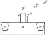
도 1은 본 개시의 다양한 양태에 따라 하나 이상의 반도체 디바이스들을 제조하는 방법(100)의 일례의 흐름도이다. 방법(100)은 예시를 목적으로 도 2 내지 도 6에 도시된 반도체 디바이스(200)를 참조하여, 이하에 상세하게 논의된다.1 is a flow diagram of one example of a
도 1 및 도 2를 참조하면, 방법(100)은 기판(210)을 제공함으로써 단계(102)에서 시작한다. 기판(210)은 벌크 실리콘 기판일 수 있다. 대안적으로, 기판(210)은 결정 구조의 실리콘 또는 게르마늄과 같은 원소 반도체; 실리콘 게르마늄, 탄화 규소, 비화 갈륨, 인화 갈륨, 인화 인듐, 비화 인듐, 및/또는 안티몬화 인듐과 같은 화합물 반도체; 또는 이들의 조합을 포함할 수 있다. 가능하게, 기판(210)은 또한 실리콘 온 인슐레이터(silicon-on-insulator; SOI) 기판을 포함한다. SOI 기판은 산소의 주입에 의한 분리(separation by implantation of oxygen; SIMOX), 웨이퍼 본딩 및/또는 다른 적합한 방법을 이용하여 제조된다.Referring to Figures 1 and 2, the
기판(210)은 당해 기술에 공지된 설계 요건에 따라 다양한 도핑된 영역들을 포함할 수 있다. 도핑된 영역은 붕소 또는 BF2와 같은 p형 도펀트; 인 또는 비소와 같은 n형 도펀트; 또는 이들의 조합으로 도핑될 수 있다. 도핑된 영역은 P웰 구조물로, N웰 구조물로, 듀얼웰 구조물로 기판(210) 상에 직접 형성되거나, 또는 돌출된 구조를 이용하여 형성될 수 있다. 기판(210)은 N형 금속 산화물 반도체 트랜지스터 디바이스를 위해 구성된 영역 및 P형 금속 산화물 반도체 트랜지스터 디바이스를 위해 구성된 영역과 같은, 다양한 활성 영역들을 더 포함할 수 있다.The
FinFET의 경우, 기판(210)은 다양한 퇴적 공정, 포토리소그래피 공정, 및/또는 에칭 공정을 포함하는 임의의 적합한 공정들에 의해 형성된 복수의 핀들을 포함할 수 있다. 예를 들어, 핀들은 기판(210)을 패턴화하고 에칭함으로써 형성된다.In the case of a FinFET, the
기판(210)은 기판(210)의 활성 영역들을 분리시키기 위해 분리 영역(212)을 포함할 수 있다. 분리 영역(212)은 쉘로우 트렌치 분리(shallow trench isolation; STI)와 같은 종래의 분리 기술을 이용하여 형성되어 다양한 영역들을 정의하고 전기적으로 분리시킬 수 있다. 분리 영역(212)은 실리콘 산화물, 실리콘 질화물, 실리콘 산화질화물, 에어 갭, 다른 적합한 물질, 또는 이들의 조합을 포함한다. 분리 영역(212)은 임의의 적합한 공정에 의해 형성된다. 일례로, STI의 형성은 포토리소그래피 공정, 기판에 트렌치를 에칭하기 위한 에칭 공정(예를 들어, 건식 에칭 및/또는 습식 에칭을 이용함), 및 하나 이상의 유전체 물질들로 트렌치 내를 충전하기 위한 퇴적 공정(예를 들어, 화학적 기상 증착 공정을 이용함)을 포함한다. 트렌치는 본 실시예에서처럼 부분적으로 충전될 수 있고, 이 경우 트렌치 사이에 남아 있는 기판은 핀 구조물을 형성한다. 일부 예에서, 충전된 트렌치는 실리콘 질화물 또는 실리콘 산화물로 충전된 열 산화 라이너층과 같은 다층 구조물을 가질 수 있다.The
도 1 및 도 2를 다시 참조하면, 방법(100)은 FinFET에서 핀들의 일부분 위(랩핑)를 포함하는, 기판(210) 위에 제 1 게이트 스택(220)을 형성하고, 제 1 게이트 스택(220)의 측벽을 따라 게이트 스페이서(225)를 형성함으로써 단계(104)로 진행한다. 제 1 게이트 스택(220)은 유전체층 및 게이트 전극층을 포함할 수 있다. 제 1 게이트 스택(220)은 퇴적 공정, 포토리소그래피 패턴화 공정 및 에칭 공정을 포함하는 절차에 의해 형성될 수 있다. 퇴적 공정들은 화학적 기상 증착(chemical vapor deposition; CVD), 물리적 기상 증착(physical vapor deposition; PVD), 원자층 증착(atomic layer deposition; ALD), 또는 다른 적합한 공정을 포함할 수 있다. 포토리소그래피 패턴화 공정은 포토레지스트 코팅(예컨대, 스핀 온 코팅), 소프트 베이킹, 마스크 정렬, 노출, 포스트 노출 베이킹, 포토레지스트 현상, 세정, 건조(예컨대, 하드 베이킹), 다른 적합한 공정, 및/또는 이들의 조합을 포함할 수 있다. 에칭 공정은 건식 에칭, 습식 에칭, 및/또는 다른 에칭 방법을 포함한다.Referring again to Figures 1 and 2, the
본 실시예에서, 제 1 게이트 스택(220)은 더미 게이트 스택이고, 제 2 게이트 스택으로 나중에 교체된다. 더미 게이트 스택(220)은 유전체층 및 폴리실리콘층을 포함할 수 있다.In this embodiment, the
게이트 스페이서(225)는 실리콘 산화물과 같은 유전체 물질을 포함한다. 대안적으로, 게이트 스페이서(225)는 실리콘 질화물, 실리콘 탄화물, 실리콘 산화질화물, 또는 이들의 조합을 포함할 수 있다. 게이트 스페이서(225)는 제 1 게이트 스택(220) 위에 유전체 물질을 퇴적하고, 그리고 나서 그 유전체 물질을 이방성 에치백(etch back)함으로써 형성될 수 있다.The
도 1 및 도 3을 참조하면, 방법(100)은 리세스(230A 및 230B)[총괄하여 리세스(230)로 언급됨]를 형성하기 위해 제 1 게이트 스택(220)의 양측에서, 핀의 일부분을 포함하는, 기판(210)의 일부분을 제거함으로써 단계(106)로 진행한다. 도시된 실시예에서, 리세스(230)는 전계 효과 트랜지스터(205)의 소스 영역 및 드레인 영역에 형성되어, 제 1 게이트 스택(220)이 리세스들(230)에 개재(interpose)되도록 한다. 이들은 소스 리세스(230A) 및 드레인 리세스(230B)로 언급된다. 리세스 공정은 습식 에칭 공정, 건식 에칭 공정, 및/또는 이들의 조합을 포함할 수 있다. 리세스 공정은 또한 선택적 습식 에칭 또는 선택적 건식 에칭을 포함할 수 있다. 습식 에칭 용액은 테트라 암모늄 하이드록시드(tetramethylammonium hydroxide; TMAH), HF/HNO3/CH3COOH 용액, 또는 다른 적합한 용액을 포함한다. 건식 에칭 공정은 풀루오린 함유 가스(예컨대, CF4, SF6, CH2F2, CHF3, 및/또는 C2F6), 염소 함유 가스(예컨대, Cl2, CHCl3, CCl4, 및/또는 BCl3), 브로민 함유 가스(예컨대, HBr 및/또는 CHBR3), 아이오딘 함유 가스, 다른 적합한 가스, 및/또는 플라즈마, 및/또는 이들의 조합을 구현할 수 있다. 에칭 공정은 에칭 선택성, 유연성 및 원하는 에칭 프로파일을 얻기 위해서 다단계 에칭을 포함할 수 있다.Referring to Figures 1 and 3, the
에칭 공정은 리세스들(230A 및 230B)의 원하는 프로파일을 달성하기 위해 제어된다. 본 실시예에서, 리세스들(230A 및 230B)의 프로파일은 도 3에 도시된 바와 같이, 제 1 게이트 스택(220) 쪽으로 향하는 면들의 적어도 하나의 꼭짓점(232A 및 232B)을 각각 갖도록 형성된다. 예로서, 꼭짓점(232A)은 (111) 결정학적 방향을 갖는 2개의 Si 면에 의해 형성된다. 제 1 거리(d1)는 2개의 가장 가까운 소스와 드레인 꼭짓점(232A 및 232B) 사이의 거리로 정의된다. 본 실시예에서, 측벽 스페이서(225)를 갖는 게이트(220)는 30 nm보다 큰 폭을 갖고, 제 1 거리(d1)는 40 nm보다 작거나 같다. 도면에서 점으로 도시되었지만, 일부 실시예들에서, 소스 및 드레인 꼭짓점(232A 및 232B)은 둥글게 될 수 있고, 10 nm보다 작거나 같은 폭을 가질 수 있다. 예로서, 둥근 꼭짓점은 포스트 리세스-에칭 열 어닐링(공정 온도 및 압력은 각각 >700 C 및 <100 torr 이다)에 의해 달성될 수 있다.The etching process is controlled to achieve the desired profile of the
도 1 및 도 4를 참조하면, 방법(100)은 리세스들(230A 및 230B)에 에피택셜 구조물들(240A 및 240B)[총괄하여 에피택셜 구조물(240)로 언급됨]을 각각 형성함으로써 단계(108)로 진행한다. 본 실시예에서, 에피택셜 구조물(240)은 소스/드레인 구조물을 포함한다. 소스/드레인 에피택셜 구조물(240)은 리세스(230)에 반도체 물질(242)을 에피택셜 성장시킴으로써 형성된다. 그 결과, 소스/드레인 에피택셜 구조물(240)의 적어도 일부분이 리세스(230)와 같은 프로파일을 갖는다.Referring to Figures 1 and 4, the
반도체 물질(242)은 게르마늄(Ge) 또는 실리콘(Si)과 같은 단일 원소 반도체 물질; 또는 갈륨 비소(GaAs), 알루미늄 갈륨 비소(AlGaAs)와 같은 화합물 반도체 물질; 또는 실리콘 게르마늄(SiGe), 갈륨 비소 인(GaAsP)과 같은 반도체 합금을 포함한다. 일 실시예에서, 반도체 물질(242)은 기판(210)의 물질과는 상이하다. 소스/드레인 에피택셜 구조물(240)은 적합한 결정학적 방향[예컨대, (100), (110), (111) 또는 (311) 결정학적 방향]을 갖는다. 예에서, NFET 디바이스가 요구되는 경우, 소스/드레인 에피택셜 구조물(240)은 에피택셜하게 성장하는 실리콘(epi Si, 또는 Si:C)(242)을 포함할 수 있다. 다른 예에서, PFET 디바이스가 요구되는 경우, 소스/드레인 에피택셜 구조물(240)은 에피택셜하게 성장하는 실리콘 게르마늄(SiGe)(242)을 포함할 수 있다. Si:C 및 SiGe는 S/D 꼭짓점을 통한 채널에 인장 변형 및 압축 변형을 제공할 수 있다. 소스/드레인 에피택셜 구조물(240)은 하나 이상의 에피택시 또는 에피택셜(epi) 공정에 의해 형성될 수 있다. 에피택셜 공정은 CVD 증착 기술[예컨대, 선택적 에피택시 성장(selective epitaxy growth; SEG), 기상 에피택시(vapor-phase epitaxy; VPE) 및/또는 초고진공 CVD(ultra-high vacuum CVD; UHV-CVD)], 분자 빔 에피택시, 및/또는 다른 적합한 공정을 포함할 수 있다.
소스/드레인 에피택셜 구조물(240)은 epi 공정 동안에 인시츄(in-situ) 도핑되거나 또는 도핑되지 않을 수 있다. 예를 들어, 에피택셜 성장된 SiGe 소스/드레인 피처(240)는 붕소로 도핑될 수 있고, 에피택셜 성장된 Si epi 소스/드레인 피처는 탄소, 인, 또는 양자 모두로 도핑될 수 있다. 소스/드레인 에피택셜 구조물(240)이 인시츄 도핑되지 않으면, 제 2 주입 공정(예컨대, 접합 주입 공정)이 수행되어 소스/드레인 에피택셜 구조물(240)을 도핑한다. 하나 이상의 어닐링 공정들이 수행되어 에피택셜 구조물에서의 소스/드레인 도펀트를 활성화시킬 수 있다. 어닐링 공정은 급속 써멀 어닐링(rapid thermal annealing; RTA) 및/또는 레이저 어닐링 공정을 포함할 수 있다.The source /
도 1 및 도 5a를 참조하면, 방법(100)은 게이트 트렌치(250)를 형성하기 위해 제 1 게이트 스택(220)을 제거하고, 핀을 포함하는 기판(210)을 더욱 에칭함으로써 단계(110)로 진행한다. 에칭 공정들은 게이트 스페이서(225)에 대하여 충분한 에칭 선택성을 갖도록 선택적 습식 에칭 또는 선택적 건식 에칭을 포함할 수 있다. 에칭 공정들은 도 3과 관련하여 앞서 논의된 것과 여러 면에서 유사할 수 있다. 본 실시예에서, 게이트 트렌치(250)는 적어도 하나의 게이트 꼭짓점(255)을 갖는 프로파일로 형성된다. 일 실시예에서, 게이트 꼭짓점(255)은 Si 기판(210)의 2개의 (111) 면들에 의해 게이트 트렌치(250)의 하부에 형성된다. 본 실시예에서, 게이트 꼭짓점(255)과 소스 및 드레인 꼭짓점(232A 및 232B)을 연결하는 수평 라인(A-A) 사이의 제 2 수직 거리(d2)는 30 nm보다 작거나 같다. 도면에서 점으로 도시되었지만, 일부 실시예들에서, 게이트 꼭짓점(255)은 둥글게 될 수 있고, 10 nm보다 작거나 같은 폭을 가질 수 있다. 예로서, 둥근 꼭짓점은 포스트 리세스-에칭 열 어닐링(<100 torr의 낮은 압력에서 >700 C의 온도)에 의해 달성될 수 있다.Referring to Figures 1 and 5A, the
다른 실시예에서, 게이트 트렌치(250)를 형성한 이후에, 이온 주입이 수행되어 기판(210)에 타겟 영역(256)을 도핑하고, 이는 도 5b에 도시된 바와 같이, 게이트 꼭짓점(255), 소스 꼭짓점(232A) 및 드레인 꼭짓점(232B) 사이에 위치한다.In another embodiment, after formation of the
도 1 및 도 6을 참조하면, 방법(100)은 게이트 트렌치(250)에 제 2 게이트 스택(260)을 형성함으로써 단계(112)로 진행한다. 제 2 게이트 스택(260)은 유전체층(262) 및 게이트 전극층(264)을 포함할 수 있다. 게이트 스택은 계면층, 캡핑층, 확산/장벽층, 유전체층, 전도성층, 다른 적합한 층, 및/또는 이들의 조합과 같은 추가의 층들을 포함할 수 있다. 예를 들어, 유전체(262)는 계면층(interfacial layer; IL) 및 게이트 유전체층을 포함할 수 있다. 예시적인 IL은 실리콘 산화물(예컨대, 열 산화물 또는 화학적 산화물) 및/또는 실리콘 산화질화물(SiON)을 포함한다. 게이트 유전체층은 실리콘 질화물, 실리콘 산화물, 실리콘 산화질화물, 하이-k(high-k) 유전체 물질, 다른 적합한 유전체 물질, 및/또는 이들의 조합과 같은 유전체 물질을 포함할 수 있다. 하이-k 유전체 물질의 예는, HfO2, HfSiO, HfSiON, HfTaO, HfTiO, HfZrO, 산화지르코늄, 산화알루미늄, HfO2-Al2O3(hafnium dioxide-alumina) 합금, 다른 적합한 하이-k 유전체 물질, 및 이들의 조합을 포함한다.Referring to Figures 1 and 6, the
게이트 전극층(264)은 폴리실리콘, 알루미늄, 구리, 티타늄, 탄탈룸, 텅스텐, 몰리브덴, 탄탈룸 질화물, 니켈 실리사이드, 코발트 실리사이드, TiN, WN, TiAl, TiAlN, TaCN, TaC, TaSiN, 금속 합금, 다른 적합한 물질, 및/또는 이들의 조합과 같은 임의의 적합한 물질을 포함한다.The
게이트 유전체층(262)과 게이트 전극층(264)은 화학적 기상 증착(CVD), 물리적 기상 증착(PVD), 원자층 증착(ALD), 또는 다른 적합한 방법, 및/또는 이들의 조합에 의해 퇴적될 수 있다.The
유전체층(270)은 소스/드레인 에피택셜 구조물(240) 및 제 2 게이트 스택(250) 위를 비롯한, 기판(210) 위에 퇴적된다. 유전체층(270)은 실리콘 산화물, 실리콘 질화물, 실리콘 탄화물, 산화질화물, 또는 다른 적합한 물질을 포함한다. 유전체층(270)은 ALD, CVD, PVD, 열 산화, 또는 이들의 조합과 같은 적합한 기술에 의해 퇴적된다. 추가적으로, CMP 공정이 수행되어, 제 2 게이트 스택(260) 및 유전체층(270)의 상부 표면을 평탄화한다.A
부가적인 단계들이 상기 방법(100) 이전에, 방법 동안에, 그리고 방법 이후에 제공될 수 있고, 기술된 단계들의 일부는 상기 방법(100)의 추가적인 실시예들을 위해 교체, 제거, 또는 이동될 수 있다. IC 디바이스(200)는 후속 처리에 의해 형성될 수 있는 추가적인 피처들을 포함할 수 있다. 예를 들어, 다양한 콘택/비아/라인 및 다층 상호접속 피처(예컨대, 금속층, 층간 유전체)가 기판 위에 형성되고, IC 디바이스(200)의 다양한 피처 또는 구조물을 접속하도록 구성될 수 있다. 예를 들어, 다층 상호접속은 종래의 비아 또는 콘택과 같은 수직 상호접속 및 금속 라인과 같은 수평 상호접속을 포함한다. 다양한 상호접속 피처들은 구리, 텅스텐 및 실리사이드를 포함하는 다양한 전도성 물질을 구현할 수 있다.Additional steps may be provided before, during, and after the
상기에 기초하여, 본 개시는 반도체 디바이스 및 그 제조를 제시한다. 반도체 디바이스는 게이트 스택, 소스 및 드레인 구조물 각각에 대해 꼭짓점 구조물을 이용한다. 게이트, 소스 및 드레인의 꼭짓점은 매우 작은 거리로 서로 분리되도록 형성된다. 반도체 디바이스는 또한 게이트 스택, 소스 및 드레인의 꼭짓점들 사이에 위치하는 도핑된 영역을 갖는 옵션이 있다. 따라서, 이러한 반도체 디바이스는 터널링 디바이스, 또는 단전자 트랜지스터(single electron transistor; SET)로서 작용할 수 있고, 작은 게이트 길이, 낮은 Vt, 낮은 소비 전력의 발전을 입증한다.Based on the above, the present disclosure presents a semiconductor device and its fabrication. Semiconductor devices use a corner structure for each of the gate stack, source and drain structures. The vertexes of the gate, the source, and the drain are formed to be separated from each other by a very small distance. The semiconductor device also has the option of having a doped region located between the vertices of the gate stack, source and drain. Thus, such a semiconductor device can act as a tunneling device, or as a single electron transistor (SET), demonstrating the development of small gate lengths, low Vt, and low power consumption.
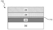
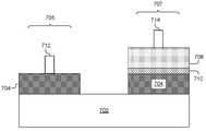
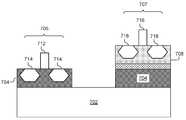
도 7a 내지 도 7h는 트랜지스터 디바이스에 임베디드 채널을 형성하기 위한 예시적인 공정을 도시하는 도면이다. 도 7a는 제 1 반도체 물질층(704)이 위에 형성된 반도체 기판(702)을 포함하는 제 1 웨이퍼(700)를 나타낸다. 반도체 기판(702)은, 예를 들어, 실리콘 온 인슐레이터(silicon-on insulator; SOI) 기판일 수 있다. 이와 같은 기판은 반도체층, 산화물층과 같은 절연체층, 및 다른 반도체층을 포함할 수 있다.7A-7H illustrate an exemplary process for forming an embedded channel in a transistor device. Figure 7A shows a
제 1 반도체 물질(704)은 NMOS 트랜지스터를 위해 설계될 수 있는 반도체 물질이다. 따라서, 반도체 유형은 N형 전도성을 가질 수 있다. 본 예에서 NMOS 트랜지스터의 채널 영역에 인장 변형과 같은, 대응 이동성을 향상시키기 위해서 채널 영역이 적절하게 변형될 수 있도록 제 1 반도체 물질(704)이 선택된다. 제 1 반도체 물질(704)은 일례에서 실리콘 게르마늄(SiGe)으로 구성될 수 있다. 제 1 반도체 물질(704)은 반도체 기판(702) 상에 에피택셜 성장될 수 있다. 일례에서, 제 1 반도체 물질(704)은 저압 화학적 기상 증착(low-pressure chemical vapor deposition; LPCVD) 공정을 이용하여 형성될 수 있다. 이와 같은 공정은 대략 섭씨 800-1100 도의 범위 내의 온도에서 일어날 수 있다. 이 공정은 대략 1-600 torr의 범위 내의 압력에서 일어날 수 있다.The
도 7b는 제 1 웨이퍼(700)에 결국 본딩될 제 2 웨이퍼(701)를 도시하는 도면이다. 제 2 웨이퍼(701)는 희생 기판(706) 및 제 2 반도체 물질층(708)을 포함한다. 희생 기판(706)은 후술되는 바와 같이 그것이 결국 제거될 것이기 때문에, 이와 같이 언급된다. 희생 기판(706)은, 예를 들어, 인듐 인화물(InP)로 구성될 수 있다.7B is a view showing a
제 2 반도체 물질(708)은 PMOS 트랜지스터 디바이스를 위해 설계될 수 있다. 따라서, 제 2 반도체 물질은 P형 전도성을 가질 수 있다. 본 예에서 PMOS 트랜지스터의 채널 영역에 압축 변형과 같은, 대응 이동성을 향상시키기 위해서 그 안에 형성된 채널 영역이 적절하게 변형될 수 있도록 제 2 반도체 물질(708)이 선택된다. 제 2 반도체 물질(708)은, 예를 들어, 인듐 갈륨 비화물(InGaAs)로 구성될 수 있다. 제 2 반도체 물질층(708)은 에피택셜 공정을 통해 형성될 수 있다. 제 2 반도체 물질층(708)은 유기 금속 화학적 기상 증착(metal-organic chemical vapor deposition; MOCVD) 공정을 이용하여 형성될 수 있다. 이와 같은 공정은 대략 섭씨 500-700 도의 범위 내의 온도에서 발생할 수 있다. 이와 같은 공정은 대략 75 torr의 압력에서 발생할 수 있다.The
도 7c는 제 1 웨이퍼(700) 및 제 2 웨이퍼(701)의 본딩 이후의 조합된 웨이퍼(703)를 도시하는 도면이다. 제 2 반도체 물질(708)이 본딩층(710)을 이용하여 제 1 반도체 물질(704)에 본딩되도록 본딩은 수행된다. 본딩이 발생하기 전에, 제 2 반도체 물질층(708)에 이용되는 물질의 유형에 따라, 표면 패시베이션 공정이 제 2 반도체 물질층(708)에 적용될 수 있다. 추가적으로, 제 1 반도체 물질층(704)에 이용되는 물질의 유형에 따라, 플라즈마 포스트 산화 공정이 제 1 채널층 물질(704) 상에 수행될 수 있다. 본딩 공정이 발생하기 이전에 도포되는 본딩층(710)은 알루미늄 산화물(Al2O3)로 구성될 수 있다. 본딩층(710)은 원자층 증착(ALD)을 통해 웨이퍼(700, 701) 양자 모두에 도포될 수 있다.Fig. 7C is a diagram showing a combined
도 7d는 희생 기판(706)의 제거를 도시하는 도면이다. 희생 기판(706)은 본딩 공정이 완료된 이후에 제거된다. 희생 기판(706)은 습식 에칭 공정을 이용하여 제거될 수 있다. 예를 들어, 염산이 희생 기판(706)을 제거하는데 이용될 수 있다.7D is a view showing the removal of the
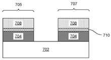
도 7e는 제 1 영역(705)에 제 1 구조물을 형성하고 제 2 영역(707)에 제 2 구조물을 형성하기 위해 조합된 웨이퍼(703)의 패턴화를 도시하는 도면이다. 후속 공정들에 걸쳐, 제 1 영역(705)의 제 1 구조물은 제 1 트랜지스터 디바이스가 될 것이고, 제 2 영역(707)의 제 2 구조물은 제 2 트랜지스터 디바이스가 될 것이다. 특히, 제 1 구조물은 NMOS 디바이스가 될 것이고, 제 2 구조물은 PMOS 디바이스가 될 것이다. 조합된 웨이퍼(703)는 다양한 포토리소그래픽 기술들을 이용하여 패턴화될 수 있다. 예를 들어, 포토레지스트가 원하는 패턴을 형성하는데 이용될 수 있다. 그런 다음, 건식 에칭 공정과 같은 이방성 에칭 공정이 패턴에 따라 노출된 조합된 웨이퍼의 일부분을 제거하는데 이용될 수 있다. 이와 같은 에칭 공정에 이용되는 에칭 가스는 염소와 질소의 혼합물 또는 염소와 아르곤의 혼합물일 수 있다. 에칭 공정에 이용되는 바이어스 전력은 25 와트 이하일 수 있다.7E is a diagram illustrating the patterning of a combined
도 7f는 제 1 영역(705)의 제 1 구조물로부터 제 2 반도체 물질(708) 및 본딩층(710)의 제거를 도시하는 도면이다. 따라서, 제 1 영역(705)의 제 1 반도체 물질층(704)은 노출된다. 제 2 반도체 물질(708)의 제거는 다양한 포토리소그래픽 기술을 수반할 수 있다. 예를 들어, 포토레지스트가 제 2 반도체 물질층(708)이 제거되도록 의도되지 않는 웨이퍼의 다른 피처 및 제 2 영역(707)을 커버하는데 이용될 수 있다. 그런 다음, 습식 에칭 공정이 제 2 반도체 물질층(708)의 노출된 부분을 제거하는데 이용될 수 있다. 습식 에칭 공정은 HCl 또는 H3PO4와 같은 다양한 습식 에칭 용액 중 하나를 포함할 수 있다.7F is a view showing the removal of the
도 7g는 게이트 구조물들(712, 716)의 형성을 도시하는 도면이다. 특히, 제 1 게이트(712)는 제 1 영역(705)에 형성되고, 제 2 게이트(716)는 제 2 영역(707)에 형성된다. 게이트 구조물(712, 716)은 다양한 제조 기술에 의해 형성될 수 있다. 일례에서, 게이트 구조물(712, 716)은 도 2 내지 도 6에 대하여 상기 기술된 게이트 디바이스와 유사한 방식으로 형성될 수 있다. 특히, 일부 예들에서, 게이트 구조물(712, 716)은 상기 기술된 바와 같은 게이트 꼭짓점을 포함할 수 있다.7G is a view showing the formation of the
도 7h는 소스/드레인 영역(714, 718)의 형성을 도시하는 도면이다. 특히, 소스/드레인 영역(714)은 제 1 영역(705)의 제 1 반도체 물질층(704) 내에 형성되고, 소스/드레인 영역(718)은 제 2 영역(707)의 제 2 반도체 물질층(708) 내에 형성된다. 소스/드레인 영역(714, 718)은 밑에 있는 반도체 물질의 일부분을 먼저 제거하고, 그런 다음, 제거된 부분 내에 소스/드레인 물질을 퇴적함으로써 형성된다.7H is a view showing the formation of the source /
소스/드레인 영역(714)은 게이트(712)의 양측 상에 리세스를 형성하기 위해 제 1 반도체 물질층(704)의 일부분을 제거함으로써 형성될 수 있다. 물질은 TMAH 습식 에칭과 같은 습식 에칭 공정에 더하여 건식 에칭 공정과 같은 이방성 에칭 공정, 또는 이들의 조합을 이용함으로써 제거될 수 있다. 제거 공정은 원하는 프로파일을 획득하기 위해 다단계 공정일 수 있다. 제거 공정 이후에, 팁이 게이트(712) 밑의 채널 영역을 향하하도록 하는 모양으로 형성되는 리세스가 있을 수 있다. 그런 다음, 이러한 리세스는 소스/드레인 물질로 충전될 수 있다. 소스/드레인 물질은 붕소와 같은 NMOS 디바이스를 위한 도펀트로 도핑된 실리콘 게르마늄일 수 있다. 소스/드레인 영역(714)은 B2H6와 같은 원하는 도펀트 유형을 함유하는 가스는 물론 실리콘 게르마늄에 기반을 둔 전구체 가스를 이용하는 LPCVD 공정을 통해 형성될 수 있다. LPCVD 공정은 대략 섭씨 300-800 도의 범위 내의 온도에서, 그리고 대략 1-500 torr의 범위 내의 압력에서 일어날 수 있다.The source /
소스/드레인 영역(718)은 게이트(716)의 양측 상에 리세스를 형성하기 위해 제 2 반도체 물질층(708)의 부분을 제거함으로써 형성될 수 있다. 물질은 H3PO4, H2O2, 또는 HCl, 또는 이들의 혼합물과 같은 다양한 습식 에천트를 이용하는 다단계 습식 에칭 공정을 이용함으로써 제거될 수 있다. [발명자: 여기서 건식 에칭 공정도 이용됨] 제거 공정 이후에, 팁이 게이트(716) 밑의 채널 영역을 향하하도록 하는 모양으로 형성되는 리세스가 있을 수 있다. 그런 다음, 이러한 리세스는 소스/드레인 물질로 충전될 수 있다. 소스/드레인 물질은 인과 같은 PMOS 디바이스를 위한 도펀트로 도핑된 실리콘 게르마늄일 수 있다. 소스/드레인 영역(718)은 PH3와 같은 원하는 도펀트 유형을 함유하는 가스는 물론 실리콘 게르마늄에 기반을 둔 전구체 가스를 이용하는 LPCVD 공정을 통해 형성될 수 있다. LPCVD 공정은 대략 섭씨 300-800 도의 범위 내의 온도에서, 그리고 대략 1-500 torr의 범위 내의 압력에서 일어날 수 있다.The source /
도 7h는 NMOS 디바이스(705) 및 PMOS 디바이스(707)이 서로 인접하게 형성되는 구조물을 나타낸다. PMOS 디바이스(707)는 NMOS 디바이스(705)와는 상이한 레벨 상에 있다. 구체적으로, PMOS 디바이스(707)는 기판(702)에 대하여 NMOS 디바이스(705)보다 높은 레벨 상에 있다. 도 7h의 피처들은 반드시 집적 회로 내에 트랜지스터의 일부일 수 있는 피처들을 모두 포함하는 것은 아님을 이해한다. 예를 들어, 추가적인 유전체층, 금속 콘택, 및 다른 피처들이 트랜지스터 디바이스의 일부이다.7H shows a structure in which
본 명세서에 기술된 원리들의 이용은 다수의 장점을 제공한다. 예를 들어, NMOS 및 PMOS 디바이스를 위해 특정 유형의 채널 물질을 이용하는 것은 더욱 효율적인 트랜지스터를 제공할 수 있다. 구체적으로, 특정 유형의 물질들은 터널링 장벽을 낮출 수 있으므로, 전압 문턱값을 낮출 수 있다. 이와 같은 트랜지스터들로 구성된 집적 회로는 동작 동안에 적은 전력을 소비할 수 있다.The use of the principles described herein provides a number of advantages. For example, using a particular type of channel material for NMOS and PMOS devices can provide more efficient transistors. Specifically, certain types of materials can lower tunneling barriers, thus lowering the voltage threshold. An integrated circuit composed of such transistors can consume less power during operation.
예를 들어, NMOS 트랜지스터의 경우, 실리콘 게르마늄 채널 및 도핑된 실리콘 게르마늄으로 구성된 소스/드레인 영역을 이용하면, 채널과 소스/드레인 영역 사이에 더욱 적은 격자 불일치가 존재한다. 이것은 소스/드레인 영역 내의 더욱 적은 전위로 이어진다. 유사하게, PMOS 트랜지스터의 경우, 채널 물질로서 인듐 갈륨 비화물을 이용하고, 소스/드레인 영역을 위해 도핑된 실리콘 게르마늄을 이용하면, 또한 더욱 적은 격자 불인치가 존재한다.For example, in the case of an NMOS transistor, using a source / drain region comprised of a silicon germanium channel and doped silicon germanium, there is less lattice mismatch between the channel and the source / drain region. This leads to fewer potentials in the source / drain regions. Similarly, for PMOS transistors, using indium gallium arsenide as the channel material and using doped silicon germanium for the source / drain regions, there is also less lattice flint.
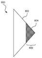
도 8은 소스/드레인 영역의 잔여 부분(802)보다 높은 도펀트 농도를 갖는 예시적인 팁(804)을 도시하는 도면(800)이다. 상기 기술된 바와 같이, 소스/드레인 영역은 채널 쪽을 향하는 꼭짓점을 갖는다. 예를 들어, 붕소로 도핑된 소스/드레인 영역을 갖는 NMOS 디바이스의 경우, 디바이스의 팁(804)에서 붕소의 농도는 더 높다. 높은 도펀트 농도를 갖는 팁(804)은, 소스/드레인 영역의 잔여 부분(802)이 형성되기 전에 형성될 수 있다. 구체적으로, 반도체 물질의 일부분이 제거된 이후에, 그리고 소스/드레인 물질이 리세스 내에 퇴적되기 전에, 높은 농도의 팁(804)은 적절한 위치에 리세스 내에 형성될 수 있다. 일례에서, 높은 도펀트 농도의 팁(804)의 두께(806)는 대략 5 나노미터이다.FIG. 8 is a drawing 800 illustrating an
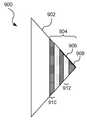
도 9는 초격자 구조물을 갖는 예시적인 팁(904)을 도시하는 도면(900)이다. 소스/드레인 영역의 잔여 부분(902)은 보통의 소스/드레인 물질일 수 있다. 초격자 구조물은 2가지 유형의 반도체 물질 간에 교호한다. 구체적으로, 초격자 구조물은 제 1 유형의 물질(906)과 제 2 유형의 물질(908) 간에 교호한다. 예를 들어, NMOS 디바이스의 경우, 제 1 물질(906)은 붕소로 도핑된 실리콘 게르마늄일 수 있고, 제 2 물질(908)은 붕소로 도핑된 실리콘일 수 있다. PMOS 디바이스의 경우, 제 1 물질(906)은 인으로 도핑된 실리콘 게르마늄일 수 있고, 제 2 물질(908)은 인으로 도핑된 실리콘일 수 있다. 일부 경우에, 2개의 상이한 물질들(906, 908)은 모두 도핑된 실리콘 게르마늄이지만, 2개의 상이한 게르마늄 농도를 가질 수 있다. 물질의 각각의 섹션의 두께(910, 912)는 대략 3 나노미터일 수 있다.9 is a drawing 900 illustrating an
소스/드레인 영역의 팁에 대하여 상기 기술을 이용하면, 전류는 채널을 통해 더욱 효율적으로 보내질 수 있다. 이것은 터널링 전압이 더욱 감소되도록 허용하므로, 트랜지스터가 더욱 낮은 전력 상에서 동작하도록 허용한다.Using the above technique for the tips of the source / drain regions, the current can be sent more efficiently through the channel. This allows the tunneling voltage to be further reduced, allowing the transistor to operate at lower power.
도 10은 개선된 채널을 갖는 트랜지스터를 형성하는 예시적인 방법을 도시하는 흐름도이다. 본 예시에 따라, 방법(1000)은 도 7h에 나타난 구조물을 형성하는데 이용될 수 있다. 방법(1000)은 반도체층 및 제 1 반도체 물질층을 포함하는 제 1 웨이퍼를 제공하기 위한 단계(1002)를 포함한다. 반도체층은 실리콘 온 인슐레이터 기판일 수 있다. 제 1 반도체 물질층은 NMOS 디바이스에 이용하기 위해 의도되는 물질일 수 있다.10 is a flow chart illustrating an exemplary method of forming a transistor with an improved channel. According to this example, the
방법(1000)은 제 1 웨이퍼를 제 2 웨이퍼에 본딩하기 위한 단계(1004)를 더 포함하고, 제 2 웨이퍼는 희생층 및 제 2 반도체 물질층을 포함한다. 제 2 채널층은 PMOS 디바이스에 이용하기 위해 의도되는 물질일 수 있다. 방법은 희생층을 제거하기 위한 단계(1006)를 더 포함한다. 이것은 웨이퍼가 본딩된 이후에 행해진다.The
방법(1000)은 제 1 영역에 제 1 구조물 및 제 2 영역에 제 2 구조물을 생성하기 위해 본딩된 기판을 패턴화하기 위한 단계(1008)를 더 포함한다. 제 1 구조물은 NMOS 디바이스를 형성하는데 이용되고, 제 2 구조물은 PMOS 디바이스를 형성하는데 이용된다. 방법(1000)은 제 1 피처로부터 제 2 반도체 물질을 제거하기 위한 단계(1010)를 더 포함한다. 이것은 제 1 반도체 물질을 노출시킨다.The
방법(1000)은 제 1 영역의 제 1 반도체 물질에 제 1 유형의 트랜지스터를 형성하기 위한 단계(1012)를 더 포함한다. 이것은 게이트 디바이스, 및 게이트 디바이스에 인접한 소스/드레인 영역을 형성하는 단계를 수반한다. 소스/드레인 영역은, 이들이 게이트 밑의 채널 영역 쪽을 향하는 꼭짓점을 갖도록 형성될 수 있다. 트랜지스터 디바이스는 도 2 내지 도 9에서 기술된 바와 같은 피처들을 가질 수 있다.The
방법(1000)은 제 2 영역의 제 2 반도체 물질에 제 2 유형의 트랜지스터를 형성하기 위한 단계(1014)를 더 포함한다. 이것은 게이트 디바이스, 및 게이트 디바이스에 인접한 소스/드레인 영역을 형성하는 단계를 수반한다. 소스/드레인 영역은, 이들이 게이트 밑의 채널 영역 쪽을 향하는 꼭짓점을 갖도록 형성될 수 있다.The
일례에 따라, 트랜지스터 디바이스는 제 1 영역 및 제 2 영역을 갖는 기판, 제 1 영역 위의 제 1 부분 및 제 2 영역 위의 제 2 부분을 갖는 제 1 반도체 물질의 제 1 반도체층을 포함하고, 제 1 부분은 제 2 부분과 분리된다. 디바이스는 제 1 반도체층의 제 2 분분 위의 제 2 반도체 물질의 제 2 반도체층, 제 1 전도성 유형의 제 1 트랜지스터, 및 제 2 전도성 유형의 제 2 트랜지스터를 더 포함하고, 제 1 트랜지스터는 제 1 반도체층에 형성된 제 1 세트의 소스/드레인 영역을 갖고 제 1 영역 내에 배치되며, 제 2 트랜지스터는 제 2 반도체층에 형성된 제 2 세트의 소스/드레인 영역을 갖고 제 2 영역 내에 배치된다. 제 1 전도성 유형은 제 2 전도성 유형과 상이하고, 제 2 반도체 물질은 제 1 반도체 물질과 상이하다.According to one example, a transistor device comprises a substrate having a first region and a second region, a first semiconductor layer of a first semiconductor material having a first portion over the first region and a second portion over the second region, The first part is separated from the second part. The device further comprises a second semiconductor layer of a second semiconductor material on a second portion of the first semiconductor layer, a first transistor of a first conductivity type, and a second transistor of a second conductivity type, Drain region and a second set of source / drain regions formed in the second semiconductor layer, and the second transistor is disposed in the second region. The first conductivity type is different from the second conductivity type, and the second semiconductor material is different from the first semiconductor material.
일례에 따라, 트랜지스터 디바이스는 게이트 디바이스, 게이트 디바이스 아래의 채널 쪽을 향하는 꼭짓점을 갖는 소스 영역, 및 채널 쪽을 향하는 꼭짓점을 갖는 드레인 영역을 포함한다. 소스 영역의 꼭짓점에서의 팁 및 드레인 영역의 꼭짓점에서의 팁은 초격자 구조물을 포함한다.According to one example, a transistor device includes a gate device, a source region having a vertex pointing towards the channel under the gate device, and a drain region having a vertex toward the channel. The tip at the apex of the tip and drain regions at the apex of the source region includes a superlattice structure.
일례에 따라, 반도체 디바이스를 제조하기 위한 방법은, 기판 및 제 1 반도체 물질층을 포함하는 제 1 웨이퍼를 제공하는 단계, 제 1 웨이퍼를 제 2 웨이퍼에 본딩하는 단계로서, 제 2 웨이퍼는 희생층 및 제 2 반도체 물질층을 포함하는 것인, 본딩 단계, 희생층을 제거하는 단계, 제 1 구조물 및 제 2 구조물을 생성하기 위해 본딩된 웨이퍼를 패턴화하는 단계, 제 1 구조물로부터 제 2 반도체 물질을 제거하는 단계, 제 1 구조물의 제 1 반도체 물질에 제 1 유형의 트랜지스터를 형성하는 단계, 및 제 2 구조물의 제 2 반도체 물질에 제 2 유형의 트랜지스터를 형성하는 단계를 포함한다.According to one example, a method for manufacturing a semiconductor device includes providing a first wafer comprising a substrate and a first layer of semiconductor material, bonding a first wafer to a second wafer, And removing the sacrificial layer, patterning the bonded wafer to produce a first structure and a second structure, depositing a second semiconductor material from the first structure, Forming a first type of transistor in the first semiconductor material of the first structure, and forming a second type of transistor in the second semiconductor material of the second structure.
당업자가 본 개시의 양태들을 더욱 잘 이해할 수 있도록 앞서 말한 것은 여러 실시예들의 특징들을 설명하였다. 당업자는 본 명세서에 도입된 실시예들의 동일한 이점들을 달성 및/또는 동일한 목적을 수행하는 구조 및 다른 공정을 설계 또는 수정하기 위한 기본으로서 본 개시를 용이하게 이용할 수 있음을 이해해야 한다. 당업자는 또한, 등가 구조물이 본 개시의 사상과 범위로부터 벗어나지 않도록 실현해야 하며, 본 개시의 사상과 범위로부터 벗어나지 않고 여기에서 다양한 변경, 대체 및 변화를 행할 수 있다.The foregoing has described features of various embodiments to enable those skilled in the art to more fully understand aspects of the disclosure. Those skilled in the art will readily appreciate that the present disclosure can readily be used as a basis for designing or modifying structures and other processes that achieve the same advantages of the embodiments introduced herein and / or perform the same purpose. Those skilled in the art should also realize that the equivalent constructions do not depart from the spirit and scope of the present disclosure and that various changes, substitutions and changes can be made herein without departing from the spirit and scope of the disclosure.
Claims (10)
Translated fromKorean제 1 영역 및 제 2 영역을 갖는 기판;
상기 제 1 영역 위의 제 1 부분 및 상기 제 2 영역 위의 제 2 부분을 갖는 제 1 반도체 물질의 제 1 반도체층 - 상기 제 1 부분은 상기 제 2 부분과 분리됨 - ;
상기 제 1 반도체층의 상기 제 2 부분 위의 제 2 반도체 물질의 제 2 반도체층;
제 1 전도성 유형의 제 1 트랜지스터 - 상기 제 1 트랜지스터는, 상기 제 1 영역 내에 배치되고, 상기 제 1 반도체층에 형성된 제 1 세트의 소스/드레인 영역들 및 상기 제 1 반도체층에 형성된 제 1 세트의 소스/드레인 영역들 사이에 형성되는 제 1 채널 영역을 가짐 - ;
제 2 전도성 유형의 제 2 트랜지스터 - 상기 제 2 트랜지스터는, 상기 제 2 영역 내에 배치되고, 상기 제 2 반도체층에 형성된 제 2 세트의 소스/드레인 영역들 및 상기 제 2 반도체층에 형성된 제 2 세트의 소스/드레인 영역들 사이에 형성되는 제 2 채널 영역을 가짐 - ; 및
상기 제 2 영역 위의 상기 제 2 채널 영역과 상기 제 1 반도체층 사이에 있는 본딩층을 포함하고,
상기 제 1 전도성 유형은 상기 제 2 전도성 유형과 상이하고, 상기 제 2 반도체 물질은 상기 제 1 반도체 물질과 상이한 것인, 트랜지스터 디바이스.In a transistor device,
A substrate having a first region and a second region;
A first semiconductor layer of a first semiconductor material having a first portion over the first region and a second portion over the second region, the first portion being separate from the second portion;
A second semiconductor layer of a second semiconductor material over the second portion of the first semiconductor layer;
A first transistor of a first conductivity type, the first transistor comprising: a first set of source / drain regions disposed in the first region and formed in the first semiconductor layer and a second set of source / A first channel region formed between the source / drain regions of the first transistor;
A second transistor of a second conductivity type, the second transistor being arranged in the second region and having a second set of source / drain regions formed in the second semiconductor layer and a second set of source / And a second channel region formed between the source / drain regions of the substrate; And
And a bonding layer between the second channel region and the first semiconductor layer over the second region,
Wherein the first conductivity type is different from the second conductivity type and the second semiconductor material is different from the first semiconductor material.
기판 및 제 1 반도체 물질층을 포함하는 제 1 웨이퍼를 제공하는 단계;
상기 제 1 웨이퍼와 제 2 웨이퍼 사이의 본딩층을 사용하여 상기 제 1 웨이퍼를 상기 제 2 웨이퍼에 본딩하는 단계로서, 상기 제 2 웨이퍼는 희생층 및 제 2 반도체 물질층을 포함하는 것인, 본딩 단계;
상기 희생층을 제거하는 단계;
제 1 구조물 및 제 2 구조물을 생성하기 위해 상기 본딩된 웨이퍼를 패터닝하는 단계;
상기 제 1 구조물로부터 상기 제 2 반도체 물질을 제거하는 단계;
상기 제 1 구조물의 상기 제 1 반도체 물질에 제 1 전도성 유형의 제 1 트랜지스터 - 상기 제 1 트랜지스터는 상기 제 1 반도체 물질에 제 1 채널 영역을 포함함 - 를 형성하는 단계; 및
상기 제 2 구조물의 상기 제 2 반도체 물질에 제 2 전도성 유형의 제 2 트랜지스터 - 상기 제 2 트랜지스터는 상기 제 2 반도체 물질에 제 2 채널 영역을 포함함 - 를 형성하는 단계를 포함하고, 상기 본딩층은 상기 제 2 구조물 내의 상기 제 2 채널 영역과 상기 제 1 반도체 물질 사이에 배치되는 것인, 반도체 디바이스를 제조하기 위한 방법.A method for fabricating a semiconductor device,
Providing a first wafer comprising a substrate and a first layer of semiconductor material;
Bonding the first wafer to the second wafer using a bonding layer between the first wafer and the second wafer, the second wafer comprising a sacrificial layer and a second layer of semiconductor material, step;
Removing the sacrificial layer;
Patterning the bonded wafer to produce a first structure and a second structure;
Removing the second semiconductor material from the first structure;
Forming a first transistor of a first conductivity type in the first semiconductor material of the first structure, the first transistor comprising a first channel region in the first semiconductor material; And
A second transistor of a second conductivity type in the second semiconductor material of the second structure, the second transistor comprising a second channel region in the second semiconductor material, Is disposed between the second channel region in the second structure and the first semiconductor material.
상기 기판에 수직인 방향으로 2개의 상이한 반도체 물질들 간에 교호하는 초격자 구조물을 형성하는 단계를 더 포함하고, 상기 2개의 상이한 반도체 물질들 모두는 같은 유형의 도펀트를 갖는 것인, 반도체 디바이스를 제조하기 위한 방법.10. The method of claim 9,
Further comprising forming an alternating superlattice structure between two different semiconductor materials in a direction perpendicular to the substrate, wherein the two different semiconductor materials all have the same type of dopant. Lt; / RTI >
Applications Claiming Priority (2)
| Application Number | Priority Date | Filing Date | Title |
|---|---|---|---|
| US201414581970A | 2014-12-23 | 2014-12-23 | |
| US14/581,970 | 2014-12-23 |
Related Child Applications (1)
| Application Number | Title | Priority Date | Filing Date |
|---|---|---|---|
| KR1020160036831ADivisionKR101697044B1 (en) | 2014-12-23 | 2016-03-28 | Improved transistor channel |
Publications (1)
| Publication Number | Publication Date |
|---|---|
| KR101657872B1true KR101657872B1 (en) | 2016-09-19 |
Family
ID=56144778
Family Applications (2)
| Application Number | Title | Priority Date | Filing Date |
|---|---|---|---|
| KR1020150012709AActiveKR101657872B1 (en) | 2014-12-23 | 2015-01-27 | Improved transistor channel |
| KR1020160036831AActiveKR101697044B1 (en) | 2014-12-23 | 2016-03-28 | Improved transistor channel |
Family Applications After (1)
| Application Number | Title | Priority Date | Filing Date |
|---|---|---|---|
| KR1020160036831AActiveKR101697044B1 (en) | 2014-12-23 | 2016-03-28 | Improved transistor channel |
Country Status (2)
| Country | Link |
|---|---|
| KR (2) | KR101657872B1 (en) |
| CN (1) | CN105720090B (en) |
Families Citing this family (2)
| Publication number | Priority date | Publication date | Assignee | Title |
|---|---|---|---|---|
| CN107910327B (en)* | 2017-11-07 | 2024-05-14 | 长鑫存储技术有限公司 | Capacitor array structure and manufacturing method thereof |
| CN112382570B (en)* | 2020-11-02 | 2024-04-26 | 上海华力集成电路制造有限公司 | Manufacturing method of PMOS |
Citations (3)
| Publication number | Priority date | Publication date | Assignee | Title |
|---|---|---|---|---|
| KR20010070298A (en)* | 2000-01-07 | 2001-07-25 | 윤종용 | CMOS Integrated circuit devices and substrates having buried silicon germanium layers therein and methods of forming same |
| KR20080032234A (en)* | 2005-07-26 | 2008-04-14 | 앰버웨이브 시스템즈 코포레이션 | Solutions for Integrated Circuit Integration of Other Active Area Materials |
| KR20100115220A (en)* | 2009-04-17 | 2010-10-27 | 삼성전자주식회사 | Inverter, method of manufacturing the same and logic circuit comprising inverter |
Family Cites Families (7)
| Publication number | Priority date | Publication date | Assignee | Title |
|---|---|---|---|---|
| US8178221B2 (en)* | 2000-07-10 | 2012-05-15 | Amit Goyal | {100}<100> or 45°-rotated {100}<100>, semiconductor-based, large-area, flexible, electronic devices |
| JP2007521650A (en)* | 2003-07-02 | 2007-08-02 | コーニンクレッカ フィリップス エレクトロニクス エヌ ヴィ | Semiconductor device, method for manufacturing quantum well structure, and semiconductor device having quantum well structure |
| US7393733B2 (en)* | 2004-12-01 | 2008-07-01 | Amberwave Systems Corporation | Methods of forming hybrid fin field-effect transistor structures |
| CN101288174A (en)* | 2005-07-15 | 2008-10-15 | 梅尔斯科技公司 | Semiconductor device including a strained superlattice and overlying stress layer and related methods |
| US7834345B2 (en)* | 2008-09-05 | 2010-11-16 | Taiwan Semiconductor Manufacturing Company, Ltd. | Tunnel field-effect transistors with superlattice channels |
| US8987748B2 (en)* | 2011-12-21 | 2015-03-24 | Texas Instruments Incorporated | Drain induced barrier lowering with anti-punch-through implant |
| CN103928336B (en)* | 2013-01-16 | 2017-05-03 | 中芯国际集成电路制造(上海)有限公司 | PMOS transistor and manufacturing method thereof |
- 2015
- 2015-01-27KRKR1020150012709Apatent/KR101657872B1/enactiveActive
- 2015-06-08CNCN201510310452.4Apatent/CN105720090B/enactiveActive
- 2016
- 2016-03-28KRKR1020160036831Apatent/KR101697044B1/enactiveActive
Patent Citations (3)
| Publication number | Priority date | Publication date | Assignee | Title |
|---|---|---|---|---|
| KR20010070298A (en)* | 2000-01-07 | 2001-07-25 | 윤종용 | CMOS Integrated circuit devices and substrates having buried silicon germanium layers therein and methods of forming same |
| KR20080032234A (en)* | 2005-07-26 | 2008-04-14 | 앰버웨이브 시스템즈 코포레이션 | Solutions for Integrated Circuit Integration of Other Active Area Materials |
| KR20100115220A (en)* | 2009-04-17 | 2010-10-27 | 삼성전자주식회사 | Inverter, method of manufacturing the same and logic circuit comprising inverter |
Also Published As
| Publication number | Publication date |
|---|---|
| CN105720090B (en) | 2019-12-03 |
| KR101697044B1 (en) | 2017-01-16 |
| CN105720090A (en) | 2016-06-29 |
Similar Documents
| Publication | Publication Date | Title |
|---|---|---|
| US10971406B2 (en) | Method of forming source/drain regions of transistors | |
| US10818661B2 (en) | Fin-like field effect transistor (FinFET) device and method of manufacturing same | |
| US10367094B2 (en) | Source/drain structure having multi-facet surfaces | |
| US10090300B2 (en) | Fin-like field effect transistor (FinFET) device and method of manufacturing same | |
| US20200321468A1 (en) | Structure of S/D Contact and Method of Making Same | |
| US9166010B2 (en) | FinFET device with epitaxial structure | |
| US10529803B2 (en) | Semiconductor device with epitaxial source/drain | |
| US9847329B2 (en) | Structure of fin feature and method of making same | |
| US10062688B2 (en) | Semiconductor device with epitaxial source/drain | |
| KR20160110908A (en) | A semiconductor device, a finfet device, and a method for fabricating the same | |
| CN113178416A (en) | Fin field effect transistor device having contact plug with recessed profile | |
| KR101697044B1 (en) | Improved transistor channel |
Legal Events
| Date | Code | Title | Description |
|---|---|---|---|
| PA0109 | Patent application | Patent event code:PA01091R01D Comment text:Patent Application Patent event date:20150127 | |
| PA0201 | Request for examination | ||
| PE0902 | Notice of grounds for rejection | Comment text:Notification of reason for refusal Patent event date:20151126 Patent event code:PE09021S01D | |
| PA0107 | Divisional application | Comment text:Divisional Application of Patent Patent event date:20160328 Patent event code:PA01071R01D | |
| PE0701 | Decision of registration | Patent event code:PE07011S01D Comment text:Decision to Grant Registration Patent event date:20160614 | |
| GRNT | Written decision to grant | ||
| PR0701 | Registration of establishment | Comment text:Registration of Establishment Patent event date:20160908 Patent event code:PR07011E01D | |
| PR1002 | Payment of registration fee | Payment date:20160908 End annual number:3 Start annual number:1 | |
| PG1601 | Publication of registration | ||
| FPAY | Annual fee payment | Payment date:20190828 Year of fee payment:4 | |
| PR1001 | Payment of annual fee | Payment date:20190828 Start annual number:4 End annual number:4 | |
| PR1001 | Payment of annual fee | Payment date:20200827 Start annual number:5 End annual number:5 | |
| PR1001 | Payment of annual fee | Payment date:20240827 Start annual number:9 End annual number:9 |