KR101656531B1 - Semiconductor device and method for manufacturing same - Google Patents
Semiconductor device and method for manufacturing sameDownload PDFInfo
- Publication number
- KR101656531B1 KR101656531B1KR1020100068394AKR20100068394AKR101656531B1KR 101656531 B1KR101656531 B1KR 101656531B1KR 1020100068394 AKR1020100068394 AKR 1020100068394AKR 20100068394 AKR20100068394 AKR 20100068394AKR 101656531 B1KR101656531 B1KR 101656531B1
- Authority
- KR
- South Korea
- Prior art keywords
- layer
- type
- region
- gate
- channel
- Prior art date
- Legal status (The legal status is an assumption and is not a legal conclusion. Google has not performed a legal analysis and makes no representation as to the accuracy of the status listed.)
- Expired - Fee Related
Links
Images


Classifications
- H—ELECTRICITY
- H10—SEMICONDUCTOR DEVICES; ELECTRIC SOLID-STATE DEVICES NOT OTHERWISE PROVIDED FOR
- H10D—INORGANIC ELECTRIC SEMICONDUCTOR DEVICES
- H10D30/00—Field-effect transistors [FET]
- H10D30/40—FETs having zero-dimensional [0D], one-dimensional [1D] or two-dimensional [2D] charge carrier gas channels
- H10D30/47—FETs having zero-dimensional [0D], one-dimensional [1D] or two-dimensional [2D] charge carrier gas channels having 2D charge carrier gas channels, e.g. nanoribbon FETs or high electron mobility transistors [HEMT]
- H10D30/471—High electron mobility transistors [HEMT] or high hole mobility transistors [HHMT]
- H10D30/475—High electron mobility transistors [HEMT] or high hole mobility transistors [HHMT] having wider bandgap layer formed on top of lower bandgap active layer, e.g. undoped barrier HEMTs such as i-AlGaN/GaN HEMTs
- H10D30/4755—High electron mobility transistors [HEMT] or high hole mobility transistors [HHMT] having wider bandgap layer formed on top of lower bandgap active layer, e.g. undoped barrier HEMTs such as i-AlGaN/GaN HEMTs having wide bandgap charge-carrier supplying layers, e.g. modulation doped HEMTs such as n-AlGaAs/GaAs HEMTs
- H—ELECTRICITY
- H10—SEMICONDUCTOR DEVICES; ELECTRIC SOLID-STATE DEVICES NOT OTHERWISE PROVIDED FOR
- H10D—INORGANIC ELECTRIC SEMICONDUCTOR DEVICES
- H10D30/00—Field-effect transistors [FET]
- H10D30/01—Manufacture or treatment
- H10D30/015—Manufacture or treatment of FETs having heterojunction interface channels or heterojunction gate electrodes, e.g. HEMT
- H—ELECTRICITY
- H10—SEMICONDUCTOR DEVICES; ELECTRIC SOLID-STATE DEVICES NOT OTHERWISE PROVIDED FOR
- H10D—INORGANIC ELECTRIC SEMICONDUCTOR DEVICES
- H10D62/00—Semiconductor bodies, or regions thereof, of devices having potential barriers
- H10D62/80—Semiconductor bodies, or regions thereof, of devices having potential barriers characterised by the materials
- H10D62/82—Heterojunctions
- H10D62/824—Heterojunctions comprising only Group III-V materials heterojunctions, e.g. GaN/AlGaN heterojunctions
- H—ELECTRICITY
- H10—SEMICONDUCTOR DEVICES; ELECTRIC SOLID-STATE DEVICES NOT OTHERWISE PROVIDED FOR
- H10D—INORGANIC ELECTRIC SEMICONDUCTOR DEVICES
- H10D84/00—Integrated devices formed in or on semiconductor substrates that comprise only semiconducting layers, e.g. on Si wafers or on GaAs-on-Si wafers
- H10D84/01—Manufacture or treatment
- H10D84/0123—Integrating together multiple components covered by H10D12/00 or H10D30/00, e.g. integrating multiple IGBTs
- H—ELECTRICITY
- H10—SEMICONDUCTOR DEVICES; ELECTRIC SOLID-STATE DEVICES NOT OTHERWISE PROVIDED FOR
- H10D—INORGANIC ELECTRIC SEMICONDUCTOR DEVICES
- H10D84/00—Integrated devices formed in or on semiconductor substrates that comprise only semiconducting layers, e.g. on Si wafers or on GaAs-on-Si wafers
- H10D84/80—Integrated devices formed in or on semiconductor substrates that comprise only semiconducting layers, e.g. on Si wafers or on GaAs-on-Si wafers characterised by the integration of at least one component covered by groups H10D12/00 or H10D30/00, e.g. integration of IGFETs
- H10D84/87—Integrated devices formed in or on semiconductor substrates that comprise only semiconducting layers, e.g. on Si wafers or on GaAs-on-Si wafers characterised by the integration of at least one component covered by groups H10D12/00 or H10D30/00, e.g. integration of IGFETs of PN-junction gate FETs
- H—ELECTRICITY
- H01—ELECTRIC ELEMENTS
- H01L—SEMICONDUCTOR DEVICES NOT COVERED BY CLASS H10
- H01L2924/00—Indexing scheme for arrangements or methods for connecting or disconnecting semiconductor or solid-state bodies as covered by H01L24/00
- H01L2924/10—Details of semiconductor or other solid state devices to be connected
- H01L2924/11—Device type
- H01L2924/13—Discrete devices, e.g. 3 terminal devices
- H01L2924/1304—Transistor
- H01L2924/1306—Field-effect transistor [FET]
- H01L2924/13064—High Electron Mobility Transistor [HEMT, HFET [heterostructure FET], MODFET]
- H—ELECTRICITY
- H10—SEMICONDUCTOR DEVICES; ELECTRIC SOLID-STATE DEVICES NOT OTHERWISE PROVIDED FOR
- H10D—INORGANIC ELECTRIC SEMICONDUCTOR DEVICES
- H10D84/00—Integrated devices formed in or on semiconductor substrates that comprise only semiconducting layers, e.g. on Si wafers or on GaAs-on-Si wafers
- H10D84/01—Manufacture or treatment
- H10D84/02—Manufacture or treatment characterised by using material-based technologies
- H10D84/05—Manufacture or treatment characterised by using material-based technologies using Group III-V technology
Landscapes
- Junction Field-Effect Transistors (AREA)
- Electrodes Of Semiconductors (AREA)
Abstract
Translated fromKorean
Description
Translated fromKorean본 발명은, 화합물 반도체계의 전계효과 트랜지스터에 관한 것으로, 특히, n형의 고(high) 전자 이동도 트랜지스터와 p형의 전계효과 트랜지스터를 동일한 화합물 반도체 기판상에 형성한 반도체 장치에 관한 것이다.Field of the Invention [0002] The present invention relates to a compound semiconductors field effect transistor, and more particularly to a semiconductor device in which an n-type high electron mobility transistor and a p-type field effect transistor are formed on the same compound semiconductor substrate.
GaAs계 등의 화합물 반도체층을 갖는 전계효과 트랜지스터는 전자 이동도가 높고, 양호한 주파수 특성을 갖기 때문에, n채널을 사용하여 휴대전화 등의 고주파 영역의 분야에서 널리 이용되고 있다. 현재, 고주파수대에 이용되는 n채널 FET(Field Effect Transistor)는, 고전자 이동도 트랜지스터(HEMT: High Electron Mobility Transistor)가 이용되고 있다. 또한, 그 변형례인, 에피택셜 성장에 의한 어느 정도의 격자 부정합을 허용하여 더욱 높은 전자 이동도를 실현하는 의사 격자 접합 고전자 이동도 트랜지스터(PHEMT: Pseudomorphic HEMT)가 알려져 있다. 또한, 게이트부에 pn접합을 형성한 JPHEMT(Junction Pseudomorphic HEMT)(예를 들면, JP-A-11-150264호 공보를 참조)가 알려져 있다. JPHEMT는, 게이트에 큰 정(正)전압을 인가하여 채널층에 형성되는 캐리어 결핍 영역을 축소하고, 채널층의 기생 저항 성분을 감소시키고 있다.A field-effect transistor having a compound semiconductor layer such as a GaAs-based compound has high electron mobility and has good frequency characteristics, and thus is widely used in the field of high-frequency region such as a cellular phone by using an n-channel. Currently, a high electron mobility transistor (HEMT) is used as an n-channel FET (Field Effect Transistor) used in a high frequency band. In addition, a pseudomorphic high electron mobility transistor (PHEMT), which is a modification thereof, realizes a higher electron mobility by permitting a certain degree of lattice mismatch by epitaxial growth. JPHEMT (Junction Pseudomorphic HEMT) (see, for example, JP-A-11-150264) in which a pn junction is formed in the gate portion is known. JPHEMT reduces a parasitic resistance component of a channel layer by reducing a carrier deficiency region formed in a channel layer by applying a large positive voltage to the gate.
이와 같이, n채널 FET의 고성능화가 진전되고 있고, 그에 더하여, 금후는 고집적화가 요구되고 있고, 화합물 반도체를 이용한 상보형 소자의 개발이 필요해지고 있다. 일반적으로, 화합물 반도체상에 n채널과 p채널의 FET를 동시에 형성하는 방법으로서, 이온 주입 기술을 사용하는 수법이 알려져 있다. 동일 기판상에 p형 도펀트와 n형 도펀트를 선택 주입하여, n채널형성 영역과 p채널형성 영역을 형성한다. 그러나, 이 이온 기술 주입법을 이용하는 경우는, 주입한 도펀트를 활성화시키기 위해, 이온 주입 후에 적어도 800℃ 이상의 고온 어닐을 행할 필요가 있다.As described above, the n-channel FETs have been made more sophisticated. In addition, high integration is required in the future, and development of complementary devices using compound semiconductors is becoming necessary. Generally, as a method for simultaneously forming n-channel and p-channel FETs on a compound semiconductor, a technique using an ion implantation technique is known. A p-type dopant and an n-type dopant are selectively implanted on the same substrate to form an n-channel formation region and a p-channel formation region. However, in the case of using this ion implantation method, it is necessary to carry out high temperature annealing at least 800 캜 or more after ion implantation in order to activate the implanted dopant.
JP-A-61-67275호 공보에는 화합물 반도체상에 n채널 FET와 p채널 FET를 동시에 형성하는 방법이 기재되어 있다. GaAs로 이루어지는 화합물 반도체 기판상에, 2차원 전자 가스를 캐리어로 하는 n채널형 헤테로 접합 전계효과 트랜지스터와, 2차원 정공 가스를 캐리어로 하는 p채널형 헤테로 접합 전계효과 트랜지스터를 형성하는 것이 기재되어 있다. n채널형 헤테로 접합 전계효과 트랜지스터는, 논 도프 GaAs층, 논 도프 AlGaAs층, n형 불순물 도프 AlGaAs층, n형 불순물 도프 GaAs층을 구비하고 있다. 각 층은 에피택셜 성장법에 의해 적층 형성되어 있다. n형 불순물 도프 AlGaAs층에는 알루미늄 또는 티탄/백금/금을 이용한 게이트 전극이, n형 불순물 도프 GaAs층에는 금 게르마늄/금을 이용한 소스·드레인 전극이 각각 형성되어 있다. p채널형 헤테로 접합 전계효과 트랜지스터는, 상기 적층 구조의 위에 논 도프 GaAs층, 논 도프 AlGaAs층, p형 불순물 도프 AlGaAs층, p형 불순물 도프 GaAs층의 각 층이 에피택셜 성장법에 의해 적층 형성되어 있다. p형 불순물 도프의 AlGaAs층에는 Al 또는 티탄/백금/금을 이용한 게이트 전극이, p형 불순물 도프의 GaAs층의 위에는 금/아연/금을 이용한 소스·드레인 전극이 각각 형성되어 있다.JP-A-61-67275 discloses a method for simultaneously forming an n-channel FET and a p-channel FET on a compound semiconductor. An n-channel hetero-junction field effect transistor using a two-dimensional electron gas as a carrier and a p-channel hetero-junction field effect transistor using a two-dimensional hole gas as a carrier are formed on a compound semiconductor substrate made of GaAs . The n-channel heterojunction field effect transistor includes a non-doped GaAs layer, a non-doped AlGaAs layer, an n-type impurity-doped AlGaAs layer, and an n-type impurity-doped GaAs layer. Each layer is laminated by the epitaxial growth method. A gate electrode made of aluminum or titanium / platinum / gold is formed on the n-type impurity doped AlGaAs layer, and source and drain electrodes made of gold germanium / gold are formed on the n-type impurity doped GaAs layer. The p-channel heterojunction field effect transistor is formed by stacking layers of a non-doped GaAs layer, a non-doped AlGaAs layer, a p-type impurity-doped AlGaAs layer, and a p-type impurity-doped GaAs layer on the laminated structure by an epitaxial growth method . Gate electrodes using Al or titanium / platinum / gold for the p-type impurity doped AlGaAs layer and source / drain electrodes using gold / zinc / gold are formed on the p-type impurity doped GaAs layer.
이온 주입 기술을 HEMT에 이용하고자 하면, 도펀트의 도핑 후에 800℃ 이상의 온도로 열처리가 필요해진다. 그러나, 헤테로 접합은 온도 600℃ 정도의 에피택셜 성장법에 의해 형성되기 때문에, 800℃ 이상의 어닐 온도에서는 헤테로 접합 계면에서 화합물 조성 원소나 불순물 원소의 상호 확산이 생겨서, 의도하는 헤테로 접합을 실현하는 것이 곤란하였다.If an ion implantation technique is to be used in a HEMT, a heat treatment is required at a temperature of 800 ° C or higher after the doping of the dopant. However, since the heterojunction is formed by the epitaxial growth method at a temperature of about 600 DEG C, mutual diffusion of the compound forming element and the impurity element occurs at the heterojunction interface at the annealing temperature of 800 DEG C or more, thereby realizing the intended heterojunction It was difficult.
또한, JP-A-61-67275호 공보에 기재된 각 전계효과 트랜지스터는, 각 게이트가 쇼트 키 접합형이다. 이 때문에, 임계치 전압을 제어하는 것, 또는 p채널의 전계효과 트랜지스터를 인핸스먼트 모드로 동작시키기가 어렵다. 그 때문에, n채널 전계효과 트랜지스터와 p채널 전계효과 트랜지스터를 동일 기판에 형성하여 리크 전류가 작은 상보형 트랜지스터를 구성하기가 어렵다는 과제가 있다.Each of the field effect transistors described in JP-A-61-67275 has a Schottky junction type gate. Therefore, it is difficult to control the threshold voltage or to operate the p-channel field-effect transistor in the enhancement mode. Therefore, there is a problem that it is difficult to form an n-channel field-effect transistor and a p-channel field-effect transistor on the same substrate to form a complementary transistor having a small leak current.
본 발명에서는 상기 과제를 해결하기 위해 이하의 수단을 강구하였다.In order to solve the above problems, the present invention has devised the following means.
본 발명의 반도체 장치는 화합물 반도체 기판과, 상기 화합물 반도체 기판의 위에 형성되고, 제 1 채널층과, 상기 제 1 채널층에 헤테로 접합하고, 상기 제 1 채널층에 n형의 전하를 공급하는 n형의 제 1 장벽층과, 상기 n형의 제 1 장벽층에 대해 pn접합형의 전위 장벽을 갖는 p형의 게이트 영역을 구비하는 n채널 전계효과 트랜지스터 영역과, 상기 화합물 반도체 기판의 위에 형성되고, p형의 제 2 채널층과, 상기 p형의 제 2 채널층에 대해 pn접합형의 전위 장벽을 갖는 n형의 게이트 영역을 포함하는 p채널 전계효과 트랜지스터 영역으로 구성된다.A semiconductor device of the present invention comprises a compound semiconductor substrate, a first channel layer formed on the compound semiconductor substrate, a first channel layer formed on the first channel layer, An n-channel field effect transistor region having a first barrier layer of a first conductivity type and a p-type gate region having a potential barrier of a pn junction type with respect to the first n-type barrier layer; and a p-channel field effect transistor region including an n-type gate region having a p-type second channel layer and a pn junction-type potential barrier with respect to the p-type second channel layer.
본 발명의 반도체 장치는, 상기 p채널 전계효과 트랜지스터 영역은, 상기 화합물 반도체 기판의 상방에, 상기 제 1 채널층, 상기 n형의 제 1 장벽층, 상기 제 2 채널층의 순서로 적층하여 형성되어 있다.The semiconductor device of the present invention is characterized in that the p-channel field effect transistor region is formed by laminating the first channel layer, the n-type first barrier layer, and the second channel layer in this order above the compound semiconductor substrate .
본 발명의 반도체 장치는, 상기 n채널 전계효과 트랜지스터 영역은, 상기 화합물 반도체 기판의 상방에, 상기 p형의 제 2 채널층, 상기 n형의 게이트 영역과 동시에 형성된 n형의 게이트층, 상기 제 1 채널층, 상기 n형의 제 1 장벽층의 순서로 적층하여 형성되어 있다.The semiconductor device of the present invention is characterized in that the n-channel field-effect transistor region includes an n-type gate layer formed simultaneously with the p-type second channel layer and the n-type gate region above the compound semiconductor substrate, One channel layer, and the n-type first barrier layer in this order.
본 발명의 반도체 장치는, 상기 n형의 게이트 영역과 상기 p형의 제 2 채널층의 사이에 게이트 리크 방지층이 형성되어 있다.In the semiconductor device of the present invention, a gate leak preventing layer is formed between the n-type gate region and the p-type second channel layer.
본 발명의 반도체 장치는, 상기 p형의 제 2 채널층에는, Zn의 확산층으로 이루어지는 p형의 소스 영역과 드레인 영역이, 상기 n형의 게이트 영역을 끼우도록 서로 이간하여 형성되어 있다.In the semiconductor device of the present invention, in the p-type second channel layer, a p-type source region and a drain region made of a Zn diffusion layer are formed so as to sandwich the n-type gate region therebetween.
본 발명의 반도체 장치는, 상기 화합물 반도체 기판과 상기 제 1 채널층의 사이에, 상기 제 1 채널층에 n형의 전하를 공급하는 n형의 제 2 장벽층이 형성되어 있다.In the semiconductor device of the present invention, an n-type second barrier layer for supplying an n-type charge to the first channel layer is formed between the compound semiconductor substrate and the first channel layer.
본 발명의 반도체 장치는, 상기 p채널 전계효과 트랜지스터 영역에는, 백 게이트 전극이 형성되어 있다.In the semiconductor device of the present invention, a back gate electrode is formed in the p-channel field effect transistor region.
본 발명의 반도체 장치는, 상기 p채널 전계효과 트랜지스터의 백 게이트 전극은, 상기 상기 n형의 제 1 장벽층상에 형성되어 있다.In the semiconductor device of the present invention, the back gate electrode of the p-channel field effect transistor is formed on the n-type first barrier layer.
본 발명의 반도체 장치의 제조 방법은, 화합물 반도체 기판상에, 제 1 버퍼층과, 제 1 채널층과, n형의 제 1 장벽층과, 제 2 버퍼층과, p형의 제 2 채널층과, n형의 게이트층을 순차로 에피택셜 성장시켜서 다층막을 형성하는 공정과, 상기 n형의 게이트층을 선택적으로 제거하여 p채널 전계효과 트랜지스터용의 n형의 게이트 영역을 형성하는 공정과, 상기 p형의 제 2 채널층을 선택적으로 제거하여, 상기 n형의 게이트 영역을 포함하는 상기 p형의 제 2 채널층이 잔류하는 p채널 전계효과 트랜지스터 영역과, 상기 n형의 제 1 장벽층이 잔류하는 n채널 전계효과 트랜지스터 영역을 구획하는 공정과, 상기 p채널 전계효과 트랜지스터 영역과 상기 n채널 전계효과 트랜지스터 영역의 노출면에 절연막을 동시에 형성하고, 상기 절연막에 제 1 개구부를 형성하는 공정과, 상기 제 1 개구부로부터 Zn 불순물을 확산시켜서, p채널 전계효과 트랜지스터용의 소스 영역 및 드레인 영역과 n채널 전계효과 트랜지스터용의 게이트 영역을 동시에 형성하는 공정과, 상기 p채널 전계효과 트랜지스터 영역과 상기 n채널 전계효과 트랜지스터 영역을 전기적으로 분리하기 위한 소자 분리 영역을 형성하는 공정과, 상기 p채널 전계효과 트랜지스터용의 상기 소스 영역 및 드레인 영역과 상기 n채널 전계효과 트랜지스터용의 게이트 영역에 금속 전극을 형성하는 공정을 포함한다.A manufacturing method of a semiconductor device of the present invention is a manufacturing method of a semiconductor device comprising a first buffer layer, a first channel layer, an n-type first barrier layer, a second buffer layer, a p- a step of sequentially epitaxially growing an n-type gate layer to form a multi-layered film; a step of selectively removing the n-type gate layer to form an n-type gate region for a p-channel field effect transistor; Type second channel layer is selectively removed to form a p-channel field effect transistor region in which the p-type second channel layer including the n-type gate region remains, and a second channel layer in which the n- Channel field effect transistor region formed in the p-channel field-effect transistor region, and a step of simultaneously forming an insulating film on the exposed surface of the p-channel field-effect transistor region and the n-channel field-effect transistor region and forming a first opening in the insulating film A step of diffusing Zn impurities from the first opening to form a source region and a drain region for a p-channel field effect transistor and a gate region for an n-channel field effect transistor at the same time, forming a device isolation region for electrically isolating the n-channel field-effect transistor region; and forming a metal electrode in the gate region for the source region and the drain region for the p-channel field-effect transistor and the gate region for the n- .
본 발명의 반도체 장치의 제조 방법은, 상기 n채널 전계효과 트랜지스터용의 소스 영역 및 드레인 영역에 금속 전극을 형성할 때에 동시에, 상기 n형의 제 1 장벽층상에 상기 p채널 전계효과 트랜지스터의 백 게이트 전극을 형성하는 공정을 포함한다.The method for fabricating a semiconductor device according to the present invention is characterized by comprising the steps of: forming a metal electrode in a source region and a drain region of the n-channel field-effect transistor and simultaneously forming, on the n-type first barrier layer, And forming an electrode.
본 발명의 반도체 장치의 제조 방법은, 화합물 반도체 기판상에, 제 1 버퍼층과, p형의 제 2 채널층과, n형의 게이트층과, n형의 제 2 장벽층과, 제 1 채널층과, n형의 제 1 장벽층을 순차로 에피택셜 성장시켜서 다층막을 형성하는 공정과, p채널 전계효과 트랜지스터 영역과 n채널 전계효과 트랜지스터 영역을 전기적으로 분리하기 위한 소자 분리 영역을 형성하는 공정과, 상기 p채널 전계효과 트랜지스터 영역의 상기 n형의 제 1 장벽층, 상기 제 1 채널층 및 상기 n형의 제 2 장벽층을 선택적으로 제거하는 공정과, 상기 p채널 전계효과 트랜지스터 영역의 상기 n형의 게이트층을 선택적으로 제거하여 p채널 전계효과 트랜지스터용의 n형의 게이트 영역을 형성하는 공정과, 상기 p채널 전계효과 트랜지스터 영역과 상기 n채널 전계효과 트랜지스터 영역의 노출면에 절연막을 동시에 형성하고, 상기 절연막에 개구부를 형성하는 공정과, 상기 개구부로부터 Zn 불순물을 확산시켜서, p채널 전계효과 트랜지스터용의 소스 영역 및 드레인 영역과 n채널 전계효과 트랜지스터용의 게이트 영역을 동시에 형성하는 공정과, 상기 p채널 전계효과 트랜지스터용의 상기 소스 영역 및 드레인 영역과 상기 n채널 전계효과 트랜지스터용의 게이트 영역에 금속 전극을 형성하는 공정을 포함한다.A manufacturing method of a semiconductor device of the present invention is a method of manufacturing a semiconductor device, comprising: forming a first buffer layer, a p-type second channel layer, an n-type gate layer, an n-type second barrier layer, And an n-type first barrier layer are sequentially epitaxially grown to form a multilayered film; a step of forming an element isolation region for electrically separating the p-channel field effect transistor region and the n-channel field effect transistor region; , Selectively removing the n-type first barrier layer, the first channel layer and the n-type second barrier layer of the p-channel field-effect transistor region; and selectively removing the n-type first barrier layer, Channel field effect transistor region is selectively removed to form an n-type gate region for a p-channel field-effect transistor; and a step of forming a p-channel field effect transistor region and an n- Forming an opening in the insulating film; diffusing Zn impurities from the opening to form a source region and a drain region for the p-channel field effect transistor and a gate region for the n-channel field effect transistor simultaneously And forming a metal electrode in the gate region for the source region and the drain region for the p-channel field effect transistor and the gate region for the n-channel field effect transistor.
본 발명의 반도체 장치의 제조 방법은, 상기 n채널 전계효과 트랜지스터용의 소스 영역 및 드레인 영역에 금속 전극을 형성할 때에 동시에, 상기 n형의 제 1 장벽층상에 상기 p채널 전계효과 트랜지스터의 백 게이트 전극을 형성하는 공정을 포함한다.The method for fabricating a semiconductor device according to the present invention is characterized by comprising the steps of: forming a metal electrode in a source region and a drain region of the n-channel field-effect transistor and simultaneously forming, on the n-type first barrier layer, And forming an electrode.
본 발명의 반도체 장치는, n채널 고전자 이동도 트랜지스터와 p채널 전계효과 트랜지스터를 동일한 화합물 반도체 기판상에 형성하였다. n채널 전계효과 트랜지스터는, 제 1 채널층과, 이 제 1 채널층에 헤테로 접합하고, 제 1 채널층에 n형의 전하를 공급하는 n형의 제 1 장벽층과, n형의 제 1 장벽층에 대해 pn접합형의 전위 장벽을 갖는 p형의 게이트 영역을 구비하고 있다. p채널 전계효과 트랜지스터는, p형의 제 2 채널층과, 이 p형의 제 2 채널층에 대해 pn접합형의 전위 장벽을 갖는 n형의 게이트 영역을 구비하고 있다. 이에 의해, 각 트랜지스터의 게이트 영역은 pn접합형의 전위 장벽을 갖고 있기 때문에, 쇼트 키 접합에 비하여 턴온 전압을 높게 하는 것이 가능해지고, 게이트 역방향 리크 전류를 감소시킬 수 있음과 함께, 임계치 전압의 제어나 인핸스먼트 모드에서의 동작을 용이하게 실현할 수 있다.In the semiconductor device of the present invention, an n-channel high electron mobility transistor and a p-channel field effect transistor are formed on the same compound semiconductor substrate. The n-channel field effect transistor includes a first channel layer, an n-type first barrier layer heterojunction to the first channel layer and supplying an n-type charge to the first channel layer, And a p-type gate region having a potential barrier of a pn junction type with respect to the layer. The p-channel field effect transistor includes a p-type second channel layer and an n-type gate region having a pn junction-type potential barrier with respect to the p-type second channel layer. As a result, since the gate region of each transistor has the potential barrier of the pn junction type, the turn-on voltage can be made higher than that of the Schottky junction, the gate inward leak current can be reduced and the threshold voltage control And the operation in the enhancement mode can be easily realized.
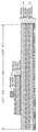
도 1은 본 발명의 실시 형태에 관한 반도체 장치의 모식적인 종단면도.
도 2는 본 발명의 다른 실시 형태에 관한 반도체 장치의 모식적인 종단면도.
도 3은 본 발명의 실시 형태에 관한 반도체 장치의 제조 방법을 도시하는 모식도.
도 4는 본 발명의 실시 형태에 관한 반도체 장치의 제조 방법을 도시하는 모식도.
도 5는 본 발명의 실시 형태에 관한 반도체 장치의 제조 방법을 도시하는 모식도.
도 6은 본 발명의 실시 형태에 관한 반도체 장치의 제조 방법을 도시하는 모식도.
도 7은 본 발명의 실시 형태에 관한 반도체 장치의 제조 방법을 도시하는 모식도.
도 8은 본 발명의 실시 형태에 관한 반도체 장치의 제조 방법을 도시하는 모식도.
도 9는 본 발명의 실시 형태에 관한 반도체 장치의 제조 방법을 도시하는 모식도.
도 10은 본 발명의 실시 형태에 관한 반도체 장치의 제조 방법을 도시하는 모식도.
도 11은 본 발명의 실시 형태에 관한 반도체 장치의 제조 방법을 도시하는 모식도.
도 12는 본 발명의 또 다른 실시 형태에 관한 반도체 장치의 모식적인 종단면도.
도 13은 본 발명의 또 다른 실시 형태에 관한 반도체 장치의 특성을 도시하는 도면.
도 14는 본 발명의 또 다른 실시 형태에 관한 반도체 장치의 제조 방법을 도시하는 모식도.
도 15는 본 발명의 또 다른 실시 형태에 관한 반도체 장치의 제조 방법을 도시하는 모식도.
도 16은 본 발명의 다른 실시 형태에 관한 반도체 장치의 모식적인 종단면도.1 is a schematic vertical cross-sectional view of a semiconductor device according to an embodiment of the present invention.
2 is a schematic vertical cross-sectional view of a semiconductor device according to another embodiment of the present invention.
3 is a schematic diagram showing a manufacturing method of a semiconductor device according to an embodiment of the present invention.
4 is a schematic diagram showing a manufacturing method of a semiconductor device according to an embodiment of the present invention.
5 is a schematic diagram showing a manufacturing method of a semiconductor device according to an embodiment of the present invention.
6 is a schematic diagram showing a manufacturing method of a semiconductor device according to an embodiment of the present invention.
7 is a schematic diagram showing a manufacturing method of a semiconductor device according to an embodiment of the present invention.
8 is a schematic diagram showing a method of manufacturing a semiconductor device according to an embodiment of the present invention.
9 is a schematic diagram showing a method of manufacturing a semiconductor device according to an embodiment of the present invention.
10 is a schematic diagram showing a manufacturing method of a semiconductor device according to an embodiment of the present invention.
11 is a schematic diagram showing a manufacturing method of a semiconductor device according to an embodiment of the present invention.
12 is a schematic vertical cross-sectional view of a semiconductor device according to still another embodiment of the present invention.
13 is a diagram showing characteristics of a semiconductor device according to still another embodiment of the present invention.
14 is a schematic diagram showing a manufacturing method of a semiconductor device according to still another embodiment of the present invention.
15 is a schematic diagram showing a manufacturing method of a semiconductor device according to still another embodiment of the present invention.
16 is a schematic vertical cross-sectional view of a semiconductor device according to another embodiment of the present invention.
본 발명에 관한 반도체 장치는, 하나의 화합물 반도체 기판상에 p채널 전계효과 트랜지스터가 형성되는 영역(이하, pFET 영역이라고 한다)과 n채널 전계효과 트랜지스터가 형성되는 영역(이하, nFET 영역이라고 한다)을 구비하고 있다.(Hereinafter referred to as an nFET region) where a p-channel field effect transistor is formed (hereinafter referred to as a pFET region) and an n-channel field effect transistor are formed on one compound semiconductor substrate, .
nFET 영역은, 화합물 반도체 기판상에 형성되는 n형 제 2 장벽층과, 제 1 채널층과, n형 제 1 장벽층과, 이 n형 제 1 장벽층에 형성된 p형 게이트 영역과, 게이트 전극을 구비하고 있다. 또한, n형 제 2 장벽층은 생략할 수 있다.The nFET region includes an n-type second barrier layer formed on the compound semiconductor substrate, a first channel layer, an n-type first barrier layer, a p-type gate region formed in the n-type first barrier layer, . In addition, the n-type second barrier layer can be omitted.
n형 제 2 장벽층과 제 1 채널층의 사이, 및 제 1 채널층과 n형 제 1 장벽층의 사이는 헤테로 접합 계면을 구성한다. n형 제 1 장벽층 및 n형 제 2 장벽층은 제 1 채널층보다도 넓은 밴드 갭을 갖고 있다. n형 제 1 장벽층과 p형 게이트 영역의 사이는 pn접합형의 전위 장벽이 생기고 있다. pn접합에 의거한 전위 장벽은 쇼트 키 장벽보다도 빌트인 전압이 크다. 그 때문에, p형 게이트 영역에, 보다 큰 정전압을 인가할 수 있다. p형 게이트 영역에 정전압을 인가하면, 제 1 채널층과 n형 제 1 장벽층 또는 n형 제 2 장벽층의 계면에 우물형 포텐셜이 구성된다. n형 제 1 장벽층 또는 n형 제 2 장벽층으로부터 이 우물형 포텐셜에 공급된 전자는 고이동도의 2차원 전자 가스로서 행동한다. 그 결과, 도시하지 않은 소스 영역과 드레인 영역 사이를 전자의 고속 이동이 가능해지고, 고속 동작의 스위칭 소자를 실현할 수 있다.a heterojunction interface is formed between the n-type second barrier layer and the first channel layer, and between the first channel layer and the n-type first barrier layer. The n-type first barrier layer and the n-type second barrier layer have a band gap wider than that of the first channel layer. a potential barrier of a pn junction type is formed between the n-type first barrier layer and the p-type gate region. The potential barrier based on the pn junction has a larger built-in voltage than the Schottky barrier. Therefore, a larger positive voltage can be applied to the p-type gate region. When a constant voltage is applied to the p-type gate region, a well potential is formed at the interface between the first channel layer and the n-type first barrier layer or the n-type second barrier layer. The electrons supplied to the well potential from the n-type first barrier layer or the n-type second barrier layer act as two-dimensional electron gases of high mobility. As a result, electrons can be moved at a high speed between a source region and a drain region, which are not shown, and high-speed switching elements can be realized.
pFET 영역은, n형 제 1 장벽층의 위에 형성되는 게이트 리크 방지층과, 제 2 채널층과, n형 게이트 영역과, 소스 영역 및 드레인 영역을 구비하고 있다. 게이트 리크 방지층을 형성하였기 때문에 게이트의 리크 전류를 저감할 수 있다. 또한, 게이트 리크 방지층은 생략할 수 있다. pFET 영역(3)과 nFET 영역(4)은 소자 분리 영역(12)에 의해 전기적으로 분리되어 있다.The pFET region has a gate leak prevention layer formed on the n-type first barrier layer, a second channel layer, an n-type gate region, and a source region and a drain region. Since the gate-leak prevention layer is formed, the leakage current of the gate can be reduced. The gate leak prevention layer may be omitted. The pFET region 3 and the nFET region 4 are electrically separated by the
n형 게이트 영역은, 제 2 채널층에 대해 pn접합형의 전위 장벽을 갖고 있다. 그 때문에, 쇼트 키형 게이트에 의한 전계효과 트랜지스터와 비교하여 게이트에 인가하는 게이트 전압을 낮게 한 인핸스먼트 모드로 구동할 수 있다. 또한, n형 게이트 영역의 불순물 농도를 조정함에 의해, 트랜지스터의 임계치 전압 제어성을 높일 수 있다. n형 게이트 영역에 부전압을 인가하여 제 2 채널층에 형성되는 공핍층의 깊이를 변화시켜서, 소스·드레인 사이에 흐르는 전류(정공)를 제어한다.The n-type gate region has a potential barrier of a pn junction type with respect to the second channel layer. Therefore, it is possible to drive in the enhancement mode in which the gate voltage applied to the gate is lower than that of the field-effect transistor by the Schottky-type gate. Further, by adjusting the impurity concentration of the n-type gate region, the threshold voltage controllability of the transistor can be enhanced. A negative voltage is applied to the n-type gate region to change the depth of the depletion layer formed in the second channel layer to control the current (hole) flowing between the source and the drain.
이와 같이, 화합물 반도체를 이용하여 pn접합형 게이트 영역을 갖는 nFET와 pFET를 동일 기판상에 형성하였기 때문에, 리크 전류가 적고 고속 동작이 가능한 상보형 FET를 고밀도로 구성할 수 있다.As described above, since the nFET and the pFET having the pn junction type gate region are formed on the same substrate by using the compound semiconductor, the complementary FET having a small leak current and capable of high-speed operation can be formed at high density.
또한, pFET를 n형 제 1 장벽층의 위에 형성하는 것에 대신하여, 화합물 반도체 기판상에 우선 제 2 채널층과 n형 게이트층 등으로 이루어지는 pFET를 형성하고, n형 게이트층의 위에 n형 제 2 장벽층, 제 1 채널층, n형 제 1 장벽층 등으로 이루어지는 nFET를 형성할 수가 있다.Alternatively, instead of forming the pFET on the n-type first barrier layer, a pFET including a second channel layer and an n-type gate layer is first formed on the compound semiconductor substrate, and an n- 2 barrier layer, a first channel layer, an n-type first barrier layer, or the like can be formed.
본 발명의 반도체 장치의 제조 방법은, 우선, 화합물 반도체 기판상에 제 1 버퍼층, 제 1 채널층, n형 제 1 장벽층, 제 2 버퍼층, p형의 제 2 채널층, 및 n형 게이트층을 순차로 적층 형성한다. 또한, n형 게이트 영역을 선택적으로 형성하여 p채널 FET용의 n형 게이트 영역을 형성하는 공정, 제 2 채널층을 선택적으로 제거하여, pFET 영역과 nFET 영역을 구획하는 공정, 표면에 절연막을 형성하는 공정을 구비하고 있다. 또한, 해당 절연막에 개구부를 형성하여 Zn 불순물을 확산시켜서 pFET용의 소스 영역과 드레인 영역과 nFET용의 게이트 영역을 동시에 형성하는 공정, pFET 영역과 nFET 영역을 분리하기 위한 소자 분리 영역을 형성하는 공정, pFET 영역에 pFET용의 소스 전극 및 드레인 전극과, nFET용의 게이트 영역에 게이트 전극을 동시에 형성하는 공정을 구비하고 있다.A method of manufacturing a semiconductor device according to the present invention is a method of manufacturing a semiconductor device comprising a first buffer layer, a first channel layer, an n-type first barrier layer, a second buffer layer, a p- Are formed in this order. A step of selectively forming an n-type gate region to form an n-type gate region for a p-channel FET; a step of selectively removing a second channel layer to partition a pFET region and an nFET region; . Forming an opening in the insulating film to diffuse Zn impurities to form a source region and a drain region for a pFET and a gate region for an nFET at the same time; forming a device isolation region for isolating the pFET region and the nFET region; , and forming a source electrode and a drain electrode for the pFET in the pFET region and a gate electrode in the gate region for the nFET simultaneously.
그 결과, 단차부의 상단측에 pFET 영역이 형성되고, 단차부의 하단측에 nFET 영역이 형성된다. 또한, 화합물 반도체 기판(2)상에 순차로 적층하는 순번을, p형의 제 2 채널층, n형 게이트층을 우선 퇴적하고, 다음에, n형 제 2 장벽층, 제 1 채널층, n형 제 1 장벽층의 순서로 적층 형성할 수가 있다. 이 경우는, 단차부의 상단측에 nFET 영역이 형성되고, 하단측에 pFET 영역이 형성된다.As a result, a pFET region is formed on the top side of the step portion, and an nFET region is formed on the bottom side of the step portion. The p-type second channel layer and the n-type gate layer are deposited first, and then the n-type second barrier layer, the first channel layer, and the n-type gate layer are sequentially stacked on the
이와 같이, pFET와 nFET를 같은 공정에서 동시에 형성할 수 있기 때문에, 제조 공수의 증가를 억제하고 저비용으로 제조할 수 있다.Thus, since the pFET and the nFET can be simultaneously formed in the same process, it is possible to suppress the increase in the number of manufacturing steps and to manufacture the device at a low cost.
(제 1 실시 형태)(First Embodiment)
도 1은, 본 발명의 제 1 실시 형태에 관한 반도체 장치의 모식적인 종단면도를 도시한다. 이하, 화합물 반도체로서 Ⅲ-V속 화합물을 이용한 예에 관해 구체적으로 설명한다. 최초에 nFET 영역(4)에 관해 설명한다. 화합물 반도체 기판(2)으로서 GaAs 단결정 기판을 사용하였다. 제 1 버퍼층(5)으로서 불순물이 첨가되지 않은 논 도프의 i-GaAs층으로 하였다. n형 제 2 장벽층(8)은 n형 전하 공급층(8a)과 고저항층(8b)의 2층구조를 갖는다. n형 전하 공급층(8a)은, n형 불순물로서 Si를 1.0×10¹² 내지 4.0×10¹²atoms/㎠의 고농도로 첨가한 두께 약 3㎚의 n+AlGaAs층으로 구성되고, 고저항층(8b)은, 불순물이 첨가되지 않은 두께 약 3㎚의 i-AlGaAs층으로 구성되어 있다. 제 1 채널층(7)은, 불순물이 첨가되지 않은 두께 5㎚ 내지 15㎚의 i-InGaAs층으로 하였다. n형 전하 공급층(8a)은 제 1 채널층(7)에 전자를 공급하기 위해 마련되어 있고, 고저항층(8b)은, 그 위의 제 1 채널층(7)과의 사이에 양호한 헤테로 접합 계면을 얻기 위해 형성되어 있다.BRIEF DESCRIPTION OF DRAWINGS FIG. 1 is a schematic vertical cross-sectional view of a semiconductor device according to a first embodiment of the present invention. FIG. Hereinafter, examples using a III-V compound as a compound semiconductor will be described in detail. First, the nFET region 4 will be described. As the
n형 제 1 장벽층(6)은, n형 전하 공급층(6a)이 고저항층(6b) 및 고저항층(6c)에 의해 끼여지는 3층구조로 구성되어 있다. 고저항층(6b)은, 불순물이 첨가되지 않은 두께 약 3㎚의 i-AlGaAs층에 의해 형성되어 있다. n형 전하 공급층(6a)은, n형 불순물로서 Si를 1.0×10¹² 내지 4.0×10¹²atoms/㎠의 고농도로 첨가된 두께 약 6㎚의 n+AlGaAs층에 의해 형성되어 있다. 고저항층(6c)은, n형 불순물로서 Si가 1.0×10¹⁰ 내지 4.0×10¹¹atoms/㎠의 저농도로 첨가된 두께 70㎚ 내지 200㎚의 n-AlGaAs층으로 형성되어 있다. n형 전하 공급층(6a)은, 제 1 채널층(7)에 전자를 공급하기 위해 마련되고, 고저항층(6b)은, 그 아래에 형성되는 제 1 채널층(7)과의 사이에 양호한 헤테로 접합 계면을 얻기 위해 마련되어 있다.The n-type
p형 게이트 영역(10)은, 고저항층(6c)의 n-AlGaAs층에 Zn을 확산한 p형 영역으로 형성되어 있다. 고저항층(6c)의 윗면에는, 실리콘 질화막으로 이루어지는 절연막(9)이 형성되고, p형 게이트 영역(10)에 Zn을 확산시키기 위한 개구부가 형성되고, 그 개구부에는 게이트 전극(11)이 형성되어 있다. 게이트 전극(11)은, 티탄(Ti), 백금(Pt), 금(Au)이 순차로 적층된 금속 전극에 의해 구성되고, 그 하부의 p형 게이트 영역(10)과 오믹 콘택트가 취하여저 있다. 또한, 도 1에서 도시하고 있지 않지만, 게이트 전극(11)을 끼우도록 소스 전극과 드레인 전극이 형성되고, 고저항층(6c)과 오밍 콘택트가 취하여저 있다.The p-
다음에, pFET 영역(3)에 관해 설명한다. pFET 영역(3)은, 고저항층(6c)까지는, nFET 영역(4)과 같은 적층 구조를 구비하고 있다. 고저항층(6c)의 위에는, 예를 들면 Si 등의 n형 불순물을 6×10¹⁸atoms/㎤ 포함하는 n+GaAs층의 캡층(26)이 형성되고, 그 위에 불순물이 첨가되지 않은 두께 10㎚ 내지 100㎚의 i-GaAs층의 제 2 버퍼층(15)이 형성되어 있다.Next, the pFET region 3 will be described. The pFET region 3 has a stacked structure similar to that of the nFET region 4 up to the
제 2 채널층(13)은, 제 2 버퍼층(15)의 위에 형성되고, 예를 들면 C(탄소) 등의 p형 불순물을 1×10¹⁶ 내지 5×10¹⁸atoms/㎤의 농도로 첨가된 두께 30㎚ 내지 250㎚의 p-GaAs층으로 구성되어 있다. 게이트 리크 방지층(14)은, 제 2 채널층(13)의 위에 형성되고, 불순물이 첨가되지 않은 두께 0㎚ 내지 50㎚의 i-AlGaAs층에 의해 구성되어 있다. n형 게이트 영역(18)은, 게이트 리크 방지층(14)의 위에 형성되는 n형 제 1 게이트층(18a)과 n형 제 2 게이트층(18b)의 2층구조를 구비하고 있다. n형 제 1 게이트층(18a)은, Si 등의 n형 불순물을 1×10¹⁷ 내지 5×10¹⁹atoms/㎤의 농도로 첨가한 두께 10㎚ 내지 50㎚의 n-InGaP로 구성되어 있다. n형 제 2 게이트층(18b)은, Si 등의 n형 불순물을 1×10¹⁷ 내지 5×10¹⁹atoms/㎤의 농도로 첨가한 두께 50 내지 200㎚의 n-GaAs에 의해 구성되어 있다.The
소스 영역 및 드레인 영역(16)은, n형 게이트 영역(18)을 끼우도록 이간하고 게이트 리크 방지층(14)을 관통하고, 제 2 채널층(13)의 일부 영역까지 연재되도록 형성되어 있다. 소스 영역 및 드레인 영역(16)은, 게이트 리크 방지층(14) 및 제 2 채널층(13)의 일부 영역에 불순물로서 Zn을 확산시킨 확산 영역에 의해 구성되어 있다. 제 2 버퍼층(15), 제 2 채널층(13), 게이트 리크 방지층(14) 및 n형 게이트 영역(18)의 측면과, 게이트 리크 방지층(14) 및 n형 게이트 영역(18)의 표면에는 실리콘 질화막으로 이루어지는 절연막(9)이 형성되어 있다. 절연막(9)에는 소스 영역 및 드레인 영역(16)에 Zn을 확산시키기 위한 개구부가 형성되고, 이 개구부에는 금속으로 이루어지는 소스 전극 및 드레인 전극(17)이 형성되고, 그 하부에 형성되는 소스 영역 및 드레인 영역(16)과 오믹 콘택트가 취하여저 있다.The source region and the
소자 분리 영역(12)은, pFET 영역(3)과 nFET 영역(4)의 경계 영역이고, n형 제 2 장벽, 제 1 채널층(7) 및 n형 제 1 장벽을 관통하도록 형성되어 있다. 소자 분리 영역(12)은, B(붕소)를 이온 주입하여 형성하였다.The
이상과 같이, pFET 영역(3)에 pn접합형 게이트를 갖는 p채널 FET를, nFET 영역에 pn접합형 게이트를 갖는 n채널 FET를 형성하였다. 이에 의해, 양 FET, 특히 p채널 FET를 인핸스 모드로 동작시킬 수 있고, 리크 전류를 저감한 고속 동작의 상보형 FET를 구성할 수 있다.As described above, the p-channel FET having the pn junction type gate is formed in the pFET region 3 and the n-channel FET having the pn junction type gate is formed in the nFET region. As a result, both FETs, particularly p-channel FETs, can be operated in the enhanced mode, and a complementary FET of a high-speed operation with reduced leakage current can be constructed.
(제 2 실시 형태)(Second Embodiment)
도 2는, 본 발명의 제 2 실시 형태에 관한 반도체 장치(20)의 모식적인 종단면도이다. 동일한 부분 또는 동일한 기능을 갖는 부분에는 같은 부호를 붙이고 있다.2 is a schematic vertical cross-sectional view of a
반도체 장치(20)는, 화합물 반도체 기판(2)의 위에 형성한 pFET 영역(3)과 nFET 영역(4)이 형성되어 있다. 우선, pFET 영역(3)을 설명한다. GaAs 단결정으로 이루어지는 화합물 반도체 기판(2)의 위에, 불순물이 첨가되지 않은 GaAs로 이루어지는 제 1 버퍼층(5)이 형성되어 있다. 제 1 버퍼층(5)의 위에, n형 불순물이 첨가된 n+GaAs로 이루어지는 캡층(26)과 불순물이 첨가되지 않은 i-GaAs로 이루어지는 제 2 버퍼층(15)이 형성되어 있다. 그 위에, p형 불순물이 첨가된 p-GaAs로 이루어지는 제 2 채널층(13)이 형성되어 있다.In the
제 2 채널층(13)상에, 불순물이 첨가되지 않은 i-AlGaAs로 이루어지는 게이트 리크 방지층(14)이 형성되어 있다. 그 위에, n형 불순물이 첨가된 n-InGaP로 이루어지는 n형 제 1 게이트층(18a)과, n형 불순물이 첨가된 n-GaAs로 이루어지는 n형 제 2 게이트층(18b)의 2층구조의 n형 게이트 영역(18)이 형성되어 있다. 소스 영역 및 드레인 영역(16)은, n형 게이트 영역(18)을 끼우도록 이간하고 게이트 리크 방지층(14)을 관통하고, 제 2 채널층(13)의 일부 영역까지 연재되도록 형성되어 있다. 소스 영역 및 드레인 영역(16)은, 게이트 리크 방지층(14) 및 제 2 채널층(13)의 일부 영역에 불순물로서 Zn을 확산시킨 확산 영역에 의해 구성되어 있다.On the
제 2 버퍼층(15), 제 2 채널층(13), 게이트 리크 방지층(14) 및 n형 게이트 영역(18)의 측면과, 게이트 리크 방지층(14) 및 n형 게이트 영역(18)의 표면에는 실리콘 질화막으로 이루어지는 절연막(9)이 형성되어 있다. 절연막(9)에는 소스 영역 및 드레인 영역(16)에 Zn을 확산시키기 위한 개구부가 형성되고, 이 개구부에는 금속으로 이루어지는 소스 전극 및 드레인 전극(17)이 형성되고, 그 하부에 형성되는 소스 영역 및 드레인 영역(16)과 오믹 콘택트가 취하여저 있다. 절연막(9)은, nFET 영역(4)이 형성되지 않은 측면, 즉 제 2 버퍼층(15), 제 2 채널층(13) 및 게이트 리크 방지층(14)의 측면에도 형성되어 있다.The side surfaces of the
다음에, nFET 영역(4)을 설명한다. 화합물 반도체 기판(2)의 위에, 제 1 버퍼층(5), 제 2 버퍼층(15), 제 2 채널층(13), 게이트 리크 방지층(14), n형 제 1 게이트층(18a) 및 n형 제 2 게이트층(18b)의 적층 구조는, pFET 영역(3)과 같은 적층 구조를 구비하고 있다. 그 위에, 불순물이 첨가되지 않은 i-AlGaAs로 이루어지는 고저항층(8c)과, 고농도의 n형 불순물이 첨가된 n+AlGaAs로 이루어지는 n형 전하 공급층(8a)과, 불순물이 첨가되지 않은 i-AlGaAs로 이루어지는 고저항층(8b)의 3층구조를 갖는 n형 제 2 장벽층(8)이 형성되어 있다. 그 위에, 불순물이 첨가되지 않은 i-InGaAs로 이루어지는 제 1 채널층(7)이 형성되어 있다. 그 위에, 불순물이 첨가되지 않은 i-AlGaAs의 고저항층(6b), 고농도 n형 불순물이 첨가된 n+AlGaAs의 n형 전하 공급층(6a), n형 불순물이 첨가된 n-AlGaAs의 고저항층(6c)으로 이루어지는 3층구조의 n형 제 1 장벽층(6)이 형성되어 있다.Next, the nFET region 4 will be described. The
p형 게이트 영역(10)은, 고저항층(6c)의 n-AlGaAs층에 Zn을 확산한 p형의 영역으로 형성되어 있다. 고저항층(6c)의 윗면에는, 실리콘 질화막으로 이루어지는 절연막(9)이 형성되고, p형 게이트 영역(10)에 Zn을 확산시키기 위한 개구부가 형성되고, 그 개구부에는 게이트 전극(11)이 형성되어 있다. 게이트 전극(11)은, 티탄(Ti), 백금(Pt), 금(Au)이 순차로 적층된 금속 전극에 의해 구성되고, 그 하부의 p형 게이트 영역(10)과 오믹 콘택트가 취하여저 있다. 또한, 도 2에서 도시하고 있지 않지만, 게이트 전극(11)을 끼우도록 소스 전극과 드레인 전극이 형성되고, 고저항층(6c)과 오밍 콘택트가 취하여저 있다.The p-
소자 분리 영역(12)은, pFET 영역(3)과 nFET 영역(4)의 경계 영역이고, n형 제 2 장벽, 제 1 채널층(7) 및 n형 제 1 장벽을 관통하도록 형성되어 있다. 또한, 소자 분리 영역(12)은, pFET 영역(3)의 측면에 형성한 절연막(9)의 표면, 및 nFET 영역(4)의 측면, 즉 제 2 버퍼층(15), 제 2 채널층(13), 게이트 리크 방지층(14), n형 게이트층(21), n형 제 2 장벽층(8), 제 1 채널층(7) 및 n형 제 1 장벽층(6)의 측면에도 형성되어 있다. 또한, 절연막(9)은 pFET 영역(3)과 nFET 영역(4)의 경계 영역에 형성한 소자 분리 영역(12)의 노출면에도 형성되어 있다.The
또한, 각 층의 막두께나 불순물이 첨가되어 있는 경우의 불순물 재료, 그 농도는, 제 1 실시 형태와 마찬가지이다.The film thickness of each layer and the impurity material and the concentration thereof in the case where impurities are added are the same as those in the first embodiment.
(제 3 실시 형태)(Third Embodiment)
도 3 내지 도 11을 이용하여 본 발명의 제 3 실시 형태에 관한 반도체 장치(1)의 제조 방법을 설명한다. 동일한 부분 또는 동일한 기능을 갖는 부분에는 같은 부호를 붙이고 있다.A manufacturing method of the
도 3은, GaAs 단결정 기판상에 GaAs 재료를 주체로 하는 각 층을, 예를 들면 MOCVD(Metal Organic Chemical Vapor Deposition)법에 의해 에피택셜 성장시킨 적층 구조를 도시하는 모식적인 종단면도이다. GaAs 단결정으로 이루어지는 화합물 반도체 기판(2)의 위에, 불순물을 첨가하지 않은 GaAs층을 에피택셜 성장시켜서 두께 약 200㎚ 정도의 제 1 버퍼층(5)을 형성한다. 그 위에, n형 불순물로서 Si를 1.0×10¹² 내지 4.0×10¹²atoms/㎠, 예를 들면 3.0×10¹²atoms/㎠의 고농도로 첨가한 n+AlGaAs층을 에피택셜 성장시켜서 두께 약 3㎚의 n형 전하 공급층(8a)을 형성한다. 다음에 불순물을 첨가하지 않은 i-AlGaAs층을 에피택셜 성장시켜서 두께 약 3㎚의 고저항층(8b)을 형성한다. n형 전하 공급층(8a)과 고저항층(8b)에 의해 n형 제 2 장벽층(8)을 구성한다. n형 제 2 장벽층(8)의 알루미늄의 조성비는 0.2 내지 0.3, 예를 들면 Al0.2Ga0.8As로 한다.Fig. 3 is a schematic vertical cross-sectional view showing a laminated structure in which each layer mainly composed of a GaAs material is epitaxially grown on a GaAs single crystal substrate by, for example, MOCVD (Metal Organic Chemical Vapor Deposition). A GaAs layer not doped with an impurity is epitaxially grown on the
다음에, n형 제 2 장벽층(8)의 위에 불순물을 첨가하지 않은 i-InGaAs층을 에피택셜 성장시켜서 두께 5㎚ 내지 15㎚의 제 1 채널층(7)을 형성한다. 제 1 채널층(7)의 인듐(In)의 조성비를 0.1 내지 0.4, 예를 들면 In0.2Ga0.8As로 하고, n형 제 2 장벽층(8)보다도 밴드 갭을 좁게 한다.Next, an i-InGaAs layer not doped with an impurity is epitaxially grown on the n-type
다음에, 제 1 채널층(7)의 위에, 불순물을 첨가하지 않은 i-AlGaAs층을 에피택셜 성장시켜서 두께 약 2㎚의 고저항층(6b)을 형성한다. 다음에 n형 불순물로서 Si를 1.0×10¹² 내지 4.0×10¹²atoms/㎠의 고농도로 첨가한 n+AlGaAs층을 에피택셜 성장시켜서 두께 약 6㎚의 n형 전하 공급층(6a)을 형성한다. 다음에 n형 불순물로서 Si를 저농도로 첨가한 n-AlGaAs층을 에피택셜 성장시켜서 두께 70㎚ 내지 200㎚의 고저항층(6c)을 형성한다. 고저항층(6b), n형 전하 공급층(6a) 및 고저항층(6c)에 의해 n형 제 1 장벽층(6)으로 한다. n형 제 1 장벽층(6)의 알루미늄의 조성비는 0.2 내지 0.3, 예를 들면 Al0.2Ga0.8As로 하고, 제 1 채널층(7)보다도 밴드 갭을 넓게 한다.Next, on the
다음에, n형 제 1 장벽층(6)의 위에 n형 불순물을 6×10¹⁸atoms/㎤ 첨가한 n+GaAs막을 에피택셜 성장시켜서 캡층(26)을 형성한다. 다음에, 불순물을 첨가하지 않은 i-GaAs층을 에피택셜 성장시켜서 두께 10㎚ 내지 100㎚의 제 2 버퍼층(15)을 형성한다.Next, an n+ GaAs film doped with 6 × 10¹⁸ atoms / cm 3 of an n-type impurity is epitaxially grown on the n-type
다음에, 제 2 버퍼층(15)의 위에, 예를 들면 C 등의 p형 불순물을 1×10¹⁶ 내지 5×10¹⁸atoms/㎤의 농도로 첨가한 p-GaAs층을 에피택셜 성장시켜서 두께 30㎚ 내지 250㎚의 제 2 채널층(13)을 형성한다. 다음에, 불순물을 첨가하지 않은 i-AlGaAs층을 에피택셜 성장시켜서 두께 0 내지 50㎚의 게이트 리크 방지층(14)을 형성한다. 두께가 0이란, 게이트 리크 방지층(14)은 필수의 구성이 아니기 때문이다. 게이트 리크 방지층(14)의 알루미늄의 조성비는 0.2 내지 0.3, 예를 들면 Al0.2Ga0.8As로 한다.Next, on the
다음에, 게이트 리크 방지층(14) 또는 제 2 채널층(13)의 위에, Si 등의 n형 불순물을 1×10¹⁷ 내지 5×10¹⁹atoms/㎤의 농도로 첨가한 n-InGaP 층을 에피택셜 성장시켜서 두께 10㎚ 내지 50㎚의 n형 제 1 게이트층(18a)을 형성한다. 다음에, Si 등의 n형 불순물을 1×10¹⁷ 내지 5×10¹⁹atoms/㎤ 첨가한 n-GaAs층을 에피털셜 성장시켜서 두께 50 내지 200㎚의 n형 제 2 게이트층(18b)을 형성한다. n형 제 1 게이트층(18a)과 n형 제 2 게이트층(18b)에 의해 n형 게이트층(21)을 구성하고 있다. 또한, 이상의 에피택셜 성장은, 온도 약 600℃에 의해 행하였다.Next, an n- InGaP layer doped with an n- type impurity such as Si at a concentration of 1 x 10¹⁷ to 5 x 10¹⁹ atoms / cm 3 is epitaxially grown on the gate-
다음에, 도 4에 도시하는 바와 같이, n형 제 2 게이트층(18b) 및 n형 제 1 게이트층(18a)을 선택적으로 에칭 제거하여, pFET 영역(3)에 n형 게이트 영역(18)을 형성한다. 포토그래피 기술 및 웨트 에칭 또는 드라이 에칭 기술을 이용하여 n형 게이트 영역(18)을 남긴다. 다음에, 도 5에 도시하는 바와 같이, 게이트 리크 방지층(14), 제 2 채널층(13), 제 2 버퍼층(15) 및 캡층(26)을 순차로 선택적으로 에칭 제거하고, 제거한 영역을 nFET 영역(4), 남긴 영역을 pFET 영역(3)으로 한다.4, the n-type
다음에, 도 6에 도시하는 바와 같이, 기판 윗면이 노출한 표면에 플라즈마 CVD법에 의해 실리콘 질화막으로 이루어지는 절연막(9)을 두께 100㎚ 내지 500㎚ 형성한다. 다음에, 도 7에 도시하는 바와 같이, 절연막(9)에, pFET 영역(3)의 소스 영역 및 드레인 영역 형성용의 제 1 개구부(22a, 22b)와, nFET 영역(4)의 게이트 영역 형성용의 제 1 개구부(22c)를 형성한다. 제 1 개구부(22a, 22b, 22c)는 포토 리소그래피 기술, 및, 예를 들면 RIE(Reactive Ion Etching) 기술을 이용한 이방성 에칭에 의해 형성한다.Next, as shown in Fig. 6, an insulating
다음에, 도 8에 도시하는 바와 같이, 절연막(9)의 제 1 개구부(22a, 22b)를 통하여 게이트 리크 방지층(14)과 제 2 채널층(13)의 두께 방향 도중까지 확산시키는 동시에, 제 1 개구부(22c)를 통하여 고저항층(6c)의 두께 방향 도중까지 확산시킨다. 이에 의해, pFET 영역(3)에 p형의 소스 영역 및 드레인 영역(16)을, nFET 영역(4)에 p형 게이트 영역(10)을 형성한다. Zn은, 디에틸징크(Zn(C2H5)2)와 아르신(AsH3)을 포함하는 가스 분위기중에서 기판을 약 600℃로 가열하고, 제 1 개구부(22a, 22b, 22c)로부터 도입 확산시킨다. 제 1 개구부(22c)의 nFET 영역(4)에서는, Zn의 확산의 깊이를 제 1 채널층(7)의 윗면부터 약 10㎚ 이상 떨어지도록 형성하는 것이 바람직하다. 또한, Zn은 이온 주입법에 의해 주입할 수도 있다.Next, as shown in Fig. 8, diffusion is made to the middle of the thickness of the gate-
다음에, 도 9에 도시하는 바와 같이, pFET 영역(3)과 nFET 영역(4)을 전기적으로 분리하기 위한 소자 분리 영역(12)을 형성한다. 소자 분리 영역(12)은, n형 제 1 장벽층(6), 제 1 채널층(7) 및 n형 제 2 장벽층(8)의 저부에 달하는 깊이까지 형성한다. 소자 분리 영역(12)은, 예를 들면 B 이온의 이온 주입법에 의해 형성할 수가 있다.Next, as shown in Fig. 9, an
다음에, 도 10에 도시하는 바와 같이, 기판의 표면에 금속막을 퇴적하고, 포토 리소그래피 기술 및 에칭 기술을 이용하여 선택적으로 제거하여, pFET 영역(3)의 소스 전극 및 드레인 전극(17)과, nFET 영역(4)의 게이트 전극(11)을 동시에 형성한다. 금속막은, 예를 들면 전자 빔 증착법에 의해 티탄(Ti), 백금(Pt), 금(Au)을 예를 들면 30㎚, 50㎚, 120㎚의 두께로 퇴적한다. 이에 의해, Zn을 확산시킨 p형의 소스 영역 및 드레인 영역(16)과 p형 게이트 영역(10)의 각각에서 오믹 콘택트를 취할 수 있다.Next, as shown in Fig. 10, a metal film is deposited on the surface of the substrate and selectively removed by photolithography and etching to form the source electrode and the
또한, 도 11에 도시하는 바와 같이, 기판 표면에 절연 재료로 이루어지는 보호막(25)을 퇴적하고, 다음에 nFET 영역(4)의 게이트 전극(11)을 끼우도록 보호막(25) 및 절연막(9)에 제 2 개구부(23)를 형성한다. 그리고, 기판 표면에 저항 가열법에 의해 금-게르마늄(AuGe) 합금을 두께 약 160㎚, 니켈(Ni)을 두께 약 40㎚ 퇴적하고, 포토 리소그래피 기술 및 에칭 기술을 이용하여 선택적으로 제거하여, 소스 전극 및 드레인 전극(24)을 형성한다. 소스 전극 및 드레인 전극(24)은 n형의 고저항층(6c)과 오믹 콘택트가 취하여저 있다. 또한, 보호막(25) 및 절연막(9)의 제 2 개구부(23)를 형성할 때에, pFET 영역(3)의 n형 게이트 영역(18)의 상부에도 동시에 개구부를 형성하고, nFET 영역(4)의 소스 전극 및 드레인 전극(24)과 동시에, pFET 영역(3)의 게이트 전극을 형성할 수가 있다.11, a
이상 설명한 제 3 실시 형태는, 도 1에 도시하는 구조의 p채널 FET와 n채널 FET를 동시에 형성하는 제조 방법이지만, 마찬가지로 도 2에 도시하는 구조의 p채널 FET와 n채널 FET를 동시에 형성할 수가 있다.The above-described third embodiment is a manufacturing method for simultaneously forming a p-channel FET and an n-channel FET having the structure shown in Fig. 1, but it is also possible to form a p-channel FET and an n- have.
(제 4 실시 형태)(Fourth Embodiment)
이하, 본 발명의 제 4 실시 형태에 관한 반도체 장치(20)의 제조 방법을 설명한다. GaAs 단결정으로 이루어지는 화합물 반도체 기판(2)의 위에, GaAs층의 제 1 버퍼층(5)을 에피택셜 성장시킨다. 다음에 n형 불순물을 고농도로 첨가한 n+GaAs의 캡층(26)과 불순물을 첨가하지 않은 i-GaAs의 제 2 버퍼층(15)을 에피택셜 성장시킨다. 다음에, p형 불순물을 첨가한 p-GaAs로 이루어지는 제 2 채널층(13)과 불순물을 첨가하지 않은 i-AlGaAs로 이루어지는 게이트 리크 방지층(14)을 에피택셜 성장시킨다. 다음에, n형 불순물을 저농도로 첨가한 n-InGaP로 이루어지는 n형 제 1 게이트층(18a)과 n형 불순물을 첨가한 n-GaAs로 이루어지는 n형 제 2 게이트층(18b)을 순차로 에피택셜 성장시켜서 n형 게이트층(21)을 형성한다.Hereinafter, a method of manufacturing the
다음에, 불순물을 첨가하지 않은 i-AlGaAs로 이루어지는 고저항층(8c)과, n형 불순물을 고농도로 첨가한 n+AlGaAs로 이루어지는 n형 전하 공급층(8a)과, 불순물을 첨가하지 않은 i-AlGaAs로 이루어지는 고저항층(8b)의 n형 제 2 장벽층(8)을 형성한다. 다음에, 불순물을 첨가하지 않은 i-InGaAs의 제 1 채널층(7)을 에피택셜 성장시킨다. 다음에, 불순물을 첨가하지 않은 i-AlGaAs의 고저항층(6b), n형 불순물을 고농도로 첨가한 n+AlGaAs의 n형 전하 공급층(6a), n형 불순물을 저농도로 첨가한 n-AlGaAs의 고저항층(6c)을 순차로 에피택셜 성장시켜서 n형 제 1 장벽층(6)을 형성한다. 이상, 각 층의 막두께나 불순물을 첨가하는 경우의 첨가 재료나 첨가 농도는 상기 제 3 실시 형태와 마찬가지이다.Next, a high-
다음에, 소자 분리 영역(12)을 형성하여 pFET 영역(3)과 nFET 영역(4)을 전기적으로 분리하고, 다음에 pFET 영역(3)의, n형 제 1 장벽층(6), 제 1 채널층(7) 및 n형 제 2 장벽층(8)을 선택적으로 제거한다. 다음에, pFET 영역(3)의 n형 게이트층(21)을 선택적으로 제거하여 n형 제 1 게이트층(18a)과 n형 제 2 게이트층(18b)의 적층 구조를 갖는 n형 게이트 영역(18)을 형성한다.Next, the
다음에, 실리콘 질화막으로 이루어지는 절연막(9)을 n형 제 1 장벽층(6)이나 게이트 리크 방지층(14)의 표면, 및 소자 분리 영역(12)의 표면에 퇴적한다. 다음에, pFET 영역(3)의 소스 영역 및 드레인 영역 형성용, 및 nFET 영역(4)의 게이트 영역 형성용의 개구부를 형성한다. 그리고, 이 개구부로부터 Zn의 p형 불순물을 게이트 리크 방지층(14) 및 제 2 채널층(13)과 고저항층(6c)에 도입하고, pFET 영역(3)에 소스 영역 및 드레인 영역(16), nFET 영역(4)에 p형 게이트 영역(10)을 각각 동시에 형성한다.Next, an insulating
다음에, 금속막을 퇴적하고 선택적으로 제거하여, pFET 영역(3)에 소스 전극 및 드레인 전극(17)과, nFET 영역(4)에 게이트 전극(11)을 동시에 형성한다. 그 밖에, pFET 영역(3)의 게이트 전극이나 nFET 영역(4)의 소스 전극 및 드레인 전극의 형성은, 상기 제 3 실시 형태와 마찬가지로 동시에 형성할 수가 있다. 또한, 에피택셜 성장에 의해 형성한 각 층의 불순물 농도나 막두께, Zn의 도입 확산, 소스 전극, 드레인 전극 및 게이트 전극의 조성이나 막두께는, 제 3 실시 형태의 경우와 마찬가지로 할 수 있다.Next, a metal film is deposited and selectively removed to form a source electrode and a
(제 5 실시예)(Fifth Embodiment)
도 12는, 본 발명의 제 5 실시 형태에 관한 반도체 장치(30)의 모식적인 종단면도이다. 상술한 동일한 부분 또는 동일한 기능을 갖는 부분에는 같은 부호를 붙이고 있다. 또한, 후술하는 백 게이트 전극(31)을 제외하고, 각 층의 막두께나 불순물이 첨가되어 있는 경우의 불순물 재료, 그 농도는, 제 1 실시 형태와 마찬가지이다.12 is a schematic vertical cross-sectional view of a
제 5 실시 형태에 관한 반도체 장치(30)는, 상기 제 1 실시 형태에 관한 반도체 장치(1)에 대해, pFET 영역(3)에 또한 백 게이트 전극(31)을 마련하고 있는 점에서 다르다. 이와 같이, p채널 FET에 백 게이트 전극(31)을 마련함에 의해, 상호 컨덕턴스가 높아지고, p채널 FET의 온/오프 특성을 향상시킬 수 있다.The
도 12에 도시하는 바와 같이, 반도체 장치(30)는, 화합물 반도체 기판(2)의 위에 pFET 영역(3)과 nFET 영역(4)이 형성되어 있다. 또한, nFET 영역(4)은, 제 1 실시 형태에 관한 반도체 장치(1)의 nFET 영역(4)과 같은 구성이고, 여기서는 설명을 생략한다.12, in the
pFET 영역(3)에서는, GaAs 단결정으로 이루어지는 화합물 반도체 기판(2)의 위에, 불순물이 첨가되지 않은 GaAs로 이루어지는 제 1 버퍼층(5)이 형성되어 있다. 제 1 버퍼층(5)의 위에, n형 제 2 장벽층(8), 제 1 채널층(7), n형 제 1 장벽층(6), 캡층(26), 제 2 버퍼층(15), 제 2 채널층(13)이 순차로 형성되어 있다. 그리고, 제 2 채널층(13)상에는, 게이트 리크 방지층(14)이나 소스 영역 및 드레인 영역(16, 16)이 형성되어 있다. 소스 영역 및 드레인 영역(16)은, 게이트 리크 방지층(14) 및 제 2 채널층(13)의 일부 영역에 불순물로서 Zn을 확산시킨 확산 영역에 의해 구성되어 있다. 또한, 게이트 리크 방지층(14)은 생략할 수 있다. pFET 영역(3)과 nFET 영역(4)은 소자 분리 영역(12)에 의해 전기적으로 분리되어 있다.In the pFET region 3, a
게이트 리크 방지층(14)상에는 n형 게이트 영역(18)이 형성되어 있고, 제 2 채널층(13)에 대해 pn접합형의 전위 장벽을 갖고 있다. 그 때문에, 쇼트 키형 게이트에 의한 전계효과 트랜지스터와 비교하여 게이트에 인가하는 게이트 전압을 낮게 한 인핸스먼트 모드로 구동할 수 있다.An n-
또한, 반도체 장치(30)의 pFET 영역(3)에서는, n형 제 1 장벽층(6)상에 백 게이트 전극(31)이 형성되어 있다. 백 게이트 전극(31)은, 예를 들면, 금-게르마늄(AuGe) 합금과 니켈(Ni)의 2층 구조로 형성할 수가 있다. 이 백 게이트 전극(31)은, 도시하지 않지만, n형 게이트 영역(18)과 전기적으로 접속된다.In the pFET region 3 of the
이 백 게이트 전극(31)은, n채널 FET의 소스 전극 및 드레인 전극(24)을 형성할 때에 동시에 생성할 수 있기 때문에, 새로운 공정이 필요 없고, 레지스트 마스크의 추가는 불필요하다.Since the
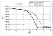
본 출원인은, 제 1 실시 형태에 관한 반도체 장치(1)의 p채널 FET의 Id-Vg 특성과 본 제 5 실시 형태에 관한 반도체 장치(30)의 p채널 FET의 Id-Vg 특성의 측정을 행하였다. 그 측정 결과를 도 13에 도시한다. 또한, 게이트 폭은 10㎛으로 하였다.The applicant of the present application measured the Id-Vg characteristic of the p-channel FET of the
이 도 13으로부터, 본 제 5 실시 형태에 관한 반도체 장치(30)의 p채널 FET의 쪽이, 제 1 실시 형태에 관한 반도체 장치(1)의 p채널 FET보다도, p채널 FET의 온/오프 특성이 향상하고 있음을 알 수 있다.13, the p-channel FET of the
예를 들면, 제 1 실시 형태에 관한 반도체 장치(1)의 p채널 FET에서는, 게이트 전압(Vg)이 0V시(온 상태)의 드레인 전류(Id)는, 4.71×10⁻⁵(A)이고, 게이트 전압(Vg)이 1V시(오프 상태) 드레인 전류(Id)는, 8.23×10⁻⁸(A)이다. 한편, 본 제 5 실시 형태에 관한 반도체 장치(30)의 p채널 FET에서는, 게이트 전압(Vg)이 0V시(온 상태)의 드레인 전류(Id)는, 5.05×10⁻⁵(A)이고, 게이트 전압(Vg)이 1V시(오프 상태)의 드레인 전류(Id)는, 1.75×10⁻¹¹(A)이다.For example, in the p-channel FET of the
또한, 본 제 5 실시 형태에 관한 반도체 장치(30)의 p채널 FET에서는, 제 1 실시 형태에 관한 반도체 장치(1)의 p채널 FET에 비하여, 게이트 전압(Vg)이 1.5V시의 드레인 전류(Id)는 커지고, 게이트 전압(Vg)이 -1V일 때의 드레인 전류(Id)는 작아진다.In the p-channel FET of the
게다가, 본 제 5 실시 형태에 관한 반도체 장치(30)의 p채널 FET에서는, 제 1 실시 형태에 관한 반도체 장치(1)의 p채널 FET에 비하여, 게이트 전압(Vg)의 변화에 대한 드레인 전류(Id)의 변화율을 크게할 수 있다.In addition, the p-channel FET of the
이와 같이, p채널 FET에 백 게이트 전극(31)을 마련함에 의해, p채널 FET의 온/오프 특성을 향상시킬 수 있다.Thus, by providing the p-channel FET with the
또한, 백 게이트 전극(31)의 레이아웃 방법은 다수 생각되지만, p채널 FET의 n형 게이트 영역(18), 소스 영역 및 드레인 영역(16)이 형성된 영역의 근처에 백 게이트 전극(31)을 형성함으로써, 레이아웃에 관계없이 같은 효과를 얻을 수 있다.Although a number of layout methods of the
다음에, 제 5 실시 형태에 관한 반도체 장치(30)의 제조 방법을 설명한다.Next, a manufacturing method of the
우선, 제 3 실시 형태와 마찬가지로, 도 3 및 도 4에서 도시하는 공정을 행한다. 또한, 이들의 공정은 제 3 실시 형태와 같기 때문에, 설명을 생략한다.First, similar to the third embodiment, the steps shown in Figs. 3 and 4 are performed. Since these steps are the same as those of the third embodiment, description thereof will be omitted.
다음에, 도 14에 도시하는 바와 같이, pFET 영역(3)중 백 게이트 전극(31)(도 12 참조)이 형성되는 영역과 nFET 영역(4)에서, 게이트 리크 방지층(14), 제 2 채널층(13), 제 2 버퍼층(15) 및 캡층(26)을 순차로 선택적으로 에칭 제거한다.Next, as shown in Fig. 14, in the region where the back gate electrode 31 (see Fig. 12) of the pFET region 3 is formed and the nFET region 4, the gate
다음에, 제 3 실시 형태와 마찬가지로, 도 6 내지 도 10에서 도시하는 공정을 행한다. 또한, 이들의 공정은 제 3 실시 형태와 같기 때문에, 설명을 생략한다.Next, as in the third embodiment, the steps shown in Figs. 6 to 10 are performed. Since these steps are the same as those of the third embodiment, description thereof will be omitted.
다음에, 도 15에 도시하는 바와 같이, 기판 표면에 절연 재료로 이루어지는 보호막(25)을 퇴적하고, 다음에 nFET 영역(4)의 게이트 전극(11)을 끼우도록 보호막(25) 및 절연막(9)에 제 2 개구부(23)를 형성한다. 동시에, pFET 영역(3)에서는, n형 제 1 장벽층(6)의 n형의 고저항층(6c)상의 보호막(25) 및 절연막(9)에 제 3 개구부(32)를 형성한다.15, a
그리고, 기판 표면에 저항 가열법에 의해 금-게르마늄(AuGe) 합금을 두께 약 160㎚, 니켈(Ni)을 두께 약 40㎚ 퇴적하고, 포토 리소그래피 기술 및 에칭 기술을 이용하여 선택적으로 제거하여, 소스 전극 및 드레인 전극(24)과 백 게이트 전극(31)을 동시에 형성한다. 이에 의해, 도 12에 도시하는 는 p채널 FET가 형성된다. 소스 전극 및 드레인 전극(24)은 n형의 고저항층(6c)과 오믹 콘택트가 취하여저 있다. 또한, 마찬가지로, 백 게이트 전극(31)은 n형의 고저항층(6c)과 오믹 콘택트가 취하여저 있다. 또한, 보호막(25) 및 절연막(9)의 제 2 개구부(23)를 형성할 때에, pFET 영역(3)의 n형 게이트 영역(18)의 상부에도 동시에 개구부를 형성하고, nFET 영역(4)의 소스 전극 및 드레인 전극(24)과 동시에, pFET 영역(3)의 게이트 전극을 형성할 수가 있다.A gold-germanium (AuGe) alloy is deposited on the surface of the substrate by a resistance heating method to a thickness of about 160 nm and nickel (Ni) to a thickness of about 40 nm and selectively removed by photolithography and etching techniques, The electrode and the
이와 같이, 백 게이트 전극(31)은, 소스 전극 및 드레인 전극(24)을 형성할 때에 동시에 형성할 수 있기 때문에, 새로운 공정이 필요 없고, 레지스트 마스크의 추가는 불필요하다.As described above, since the
(제 6 실시예)(Sixth Embodiment)
도 16은, 본 발명의 제 6 실시 형태에 관한 반도체 장치(40)의 모식적인 종단면도이다. 상술한 동일한 부분 또는 동일한 기능을 갖는 부분에는 같은 부호를 붙이고 있다. 또한, 후술하는 백 게이트 전극(31) 및 n-GaAs층(41)을 제외하고, 각 층의 막두께나 불순물이 첨가되어 있는 경우의 불순물 재료, 그 농도는, 제 2 실시 형태와 마찬가지이다.16 is a schematic vertical cross-sectional view of a
제 6 실시 형태에 관한 반도체 장치(40)는, 상기 제 2 실시 형태에 관한 반도체 장치(20)에 대해, 제 1 버퍼층(5)과 캡층(26)의 사이에 n-GaAs층(41)을 형성하고, 또한, pFET 영역(3)에서의 n-GaAs층(41)상에 백 게이트 전극(31)을 마련하고 있는 점에서 다르다. 이와 같이, p채널 FET에 백 게이트 전극(31)을 마련함에 의해, 상호 컨덕턴스가 높아지고, p채널 FET의 온/오프 특성을 향상시킬 수 있다.The
도 16에 도시하는 바와 같이, 반도체 장치(40)에서는, 화합물 반도체 기판(2)의 위에 pFET 영역(3)과 nFET 영역(4)이 형성되어 있다. 또한, nFET 영역(4)은, 제 2 실시 형태에 관한 반도체 장치(10)의 nFET 영역(4)과 같은 구성이고, 여기서는 설명을 생략한다.16, in the
pFET 영역(3)에서는, GaAs 단결정으로 이루어지는 화합물 반도체 기판(2)의 위에, 불순물이 첨가되지 않은 GaAs로 이루어지는 제 1 버퍼층(5)이 형성되어 있다. 그리고, 제 1 버퍼층(5)의 위에, n형 불순물로서 Si가 1.0×10 내지 4.0×10¹¹atoms/㎠의 저농도로 첨가된 n-GaAs로 이루어지는 n-GaAs층(41)이 형성된다.In the pFET region 3, a
또한, 이 n-GaAs층(41)상에는, 반도체 장치(20)와 마찬가지로, 캡층(26), 제 2 버퍼층(15), 제 2 채널층(13)이 순차로 형성되어 있다. 그리고, 제 2 채널층(13)상에는, 게이트 리크 방지층(14)이나 소스 영역 및 드레인 영역(16, 16)이 형성되어 있다. 소스 영역 및 드레인 영역(16)은, 게이트 리크 방지층(14) 및 제 2 채널층(13)의 일부 영역에 불순물로서 Zn을 확산시킨 확산 영역에 의해 구성되어 있다. 또한, 게이트 리크 방지층(14)은 생략할 수 있다. pFET 영역(3)과 nFET 영역(4)은 소자 분리 영역(12)에 의해 전기적으로 분리되어 있다.A
또한, 반도체 장치(40)에서는, n형 제 1 장벽층(6)상에 백 게이트 전극(31)이 형성되어 있다. 백 게이트 전극(31)은, 예를 들면, 금-게르마늄(AuGe) 합금과 니켈(Ni)의 2층 구조로 형성할 수가 있다. 이 백 게이트 전극(31)은, 도시하지 않지만, n형 게이트 영역(18)과 전기적으로 접속된다.In the
이와 같이, 반도체 장치(40)에서는, 반도체 장치(30)와 마찬가지로 백 게이트 전극(31)을 형성하고 있고, p채널 FET의 온/오프 특성을 향상시킬 수 있다.As described above, in the
다음에, 제 6 실시 형태에 관한 반도체 장치(40)의 제조 방법을 설명한다.Next, a manufacturing method of the
우선, GaAs 단결정으로 이루어지는 화합물 반도체 기판(2)의 위에, GaAs층의 제 1 버퍼층(5)을 에피택셜 성장시킨다. 다음에, n형 불순물로서 Si가 1.0×10¹⁰ 내지 4.0×10¹¹atoms/㎠의 저농도로 첨가된 n-GaAs로 이루어지는 n-GaAs층(41)을 에피택셜 성장시킨다. 그 후, 제 4 실시예와 마찬가지로, 캡층(26), 제 2 버퍼층(15), 제 2 채널층(13), 게이트 리크 방지층(14)을 순차로 에피택셜 성장시키고, 그 후, n형 제 1 게이트층(18a)과 n형 제 2 게이트층(18b)을 순차로 에피택셜 성장시켜서 n형 게이트층(21)을 형성한다.First, a
다음에, 제 4 실시예와 마찬가지로, 저항층(8b)과, n형 전하 공급층(8a)과, n형 제 2 장벽층(8), 제 1 채널층(7), n형 제 1 장벽층(6)을 형성하고, 소자 분리 영역(12)을 형성하여 pFET 영역(3)과 nFET 영역(4)을 전기적으로 분리한다.Next, as in the fourth embodiment, a
다음에, pFET 영역(3)의, n형 제 1 장벽층(6), 제 1 채널층(7) 및 n형 제 2 장벽층(8)을 선택적으로 제거한다. 또한, pFET 영역(3)의 백 게이트 전극 형성 영역상의 게이트 리크 방지층(14), 제 2 채널층(13), 제 2 버퍼층(15), 캡층(26)을 선택적으로 제거한다.Next, the n-type
다음에, 제 4 실시예와 마찬가지로, n형 게이트 영역(18)을 형성하고, 실리콘 질화막으로 이루어지는 절연막(9)을 n형 제 1 장벽층(6)이나 게이트 리크 방지층(14)의 표면, n-GaAs층(41)의 표면, 및 소자 분리 영역(12)의 표면에 퇴적한다. 다음에, 제 4 실시예와 마찬가지로, 절연막(9)을 선택적으로 개구하여 개구부를 형성하고, 이 개구부로부터 Zn의 p형 도펀트를 도입하여, pFET 영역(3)에 소스 영역 및 드레인 영역(16), nFET 영역(4)에 p형 게이트 영역(10)을 각각 동시에 형성한다. 다음에, 제 4 실시예와 마찬가지로, 금속막을 퇴적하고 선택적으로 제거하여, pFET 영역(3)에 소스 전극 및 드레인 전극(17)과, nFET 영역(4)에 게이트 전극(11)을 동시에 형성한다.Next, an n-
다음에, 기판 표면에 절연 재료로 이루어지는 보호막(25)을 퇴적하고, nFET 영역(4)의 게이트 전극(11)을 끼우도록 보호막(25) 및 절연막(9)에 제 2 개구부(23)를 형성한다. 동시에, pFET 영역(3)에서는, n형 제 1 장벽층(6)의 n형의 고저항층(6c)상의 보호막(25) 및 절연막(9)에 제 3 개구부(32)를 형성한다.Next, a
그리고, 기판 표면에 저항 가열법에 의해 금-게르마늄(AuGe) 합금을 두께 약 160㎚, 니켈(Ni)을 두께 약 40㎚ 퇴적하고, 포토 리소그래피 기술 및 에칭 기술을 이용하여 선택적으로 제거하여, 소스 전극 및 드레인 전극(24)과 백 게이트 전극(31)을 동시에 형성한다. 이에 의해, 도 16에 도시하는 는 p채널 FET가 형성된다. 소스 전극 및 드레인 전극(24)은 n형의 고저항층(6c)과 오믹 콘택트가 취하여저 있다. 또한, 마찬가지로, 백 게이트 전극(31)은 n형의 고저항층(6c)과 오믹 콘택트가 취하여저 있다. 또한, 보호막(25) 및 절연막(9)의 제 2 개구부(23)를 형성할 때에, pFET 영역(3)의 n형 게이트 영역(18)의 상부에도 동시에 개구부를 형성하고, nFET 영역(4)의 소스 전극 및 드레인 전극(24)과 동시에, pFET 영역(3)의 게이트 전극을 형성할 수가 있다.A gold-germanium (AuGe) alloy is deposited on the surface of the substrate by a resistance heating method to a thickness of about 160 nm and nickel (Ni) to a thickness of about 40 nm and selectively removed by photolithography and etching techniques, The electrode and the
이상과 같이, 본 발명의 반도체 장치(1, 20, 30, 40)의 제조 방법에 의하면, 화합물 반도체 기판(2)상에 p채널 FET와 n채널 FET를 동시에 형성할 수가 있다. 게다가, p채널 FET의 p형의 제 2 채널층(13)에 대해 n형 게이트 영역(18)으로 하고, 또한 n채널 FET의 n형 제 1 장벽층(6)에 대해 p형 게이트 영역(10)으로 하는 pn접합형의 게이트 영역을 동시에 형성할 수가 있다. 즉, 인핸스먼트 모드의 상보형 FET를 동시에 구성할 수 있기 때문에, 리크 전류를 감소시킨 고속 동작이 가능한 상보형 FET를 하나의 화합물 반도체 기판에 고밀도로 제조하는 것이 가능해진다.As described above, according to the manufacturing method of the semiconductor device (1, 20, 30, 40) of the present invention, the p-channel FET and the n-channel FET can be simultaneously formed on the
본 출원은 JP2009-180653호(2009.08.03) 및 JP2010-031710GH(2010.02.16)의 우선권주장출원이다.This application is a priority claim of JP2009-180653 (2009.08.03) and JP2010-031710GH (Feb. 16, 2010).
이상 본 발명을 상기 실시예에 입각하여 설명하였지만, 본 발명은 상기 실시예의 구성에만 한정되는 것이 아니고, 특허청구의 범위의 각 청구항의 발명의 범위 내에서 당업자라면 행할 수 있는 각종 변형, 수정을 포함하는 것은 물론이다.While the present invention has been described with reference to the above embodiments, it is to be understood that the invention is not limited to the disclosed exemplary embodiments, but includes various variations and modifications which may be made by those skilled in the art within the scope of the invention. Of course.
Claims (12)
Translated fromKorean화합물 반도체 기판과,
상기 화합물 반도체 기판의 위에 형성되고, 제 1 채널층과, 상기 제 1 채널층에 헤테로 접합하고, 상기 제 1 채널층에 n형의 전하를 공급하는 n형의 제 1 장벽층과, 상기 n형의 제 1 장벽층에 대해 pn접합형의 전위 장벽을 갖는 p형의 게이트 영역을 구비하는 n채널 전계효과 트랜지스터 영역과,
상기 n형의 제 1 장벽층의 위에 형성되고, p형의 제 2 채널층과, 게이트 리크 방지층과, 상기 p형의 제 2 채널층에 대해 pn접합형의 전위 장벽을 갖는 n형의 게이트 영역을 포함하는 p채널 전계효과 트랜지스터 영역으로 구성되고,
상기 p형의 제 2 채널층에는, Zn의 확산층으로 이루어지는 p형의 소스 영역과 드레인 영역이, 상기 n형의 게이트 영역을 끼우도록 서로 이간하여 형성되고,
상기 제 1 채널층은, 불순물이 첨가되지 않은 i-InGaAs층이고,
상기 n형의 제 1 장벽층은, 상기 제 1 채널층의 측부터 차례로, 상기 제 1 채널층과의 사이에 양호한 헤테로 접합 계면을 얻기 위해 마련된 불순물이 첨가되지 않은 제 1 고저항층으로서의 i-AlGaAs층, 상기 제 1 채널층에 전자를 공급하기 위해 마련된 n형 불순물이 첨가된 n형 전하 공급층으로서의 n+AlGaAs층, n형 불순물이 첨가된 제 2 고저항층으로서의 n-AlGaAs층의 순서로 적층하여 형성되고,
상기 p형의 게이트 영역은, 상기 제 2 고저항층에 Zn을 확산한 p형 영역으로 형성되고,
상기 p형의 제 2 채널층은, 상기 n형의 제 1 장벽층의 위에 형성된 n형 불순물을 포함하는 캡층으로서의 n+GaAs층과 그 위에 형성된 버퍼층으로서의 불순물이 첨가되지 않은 i-GaAs층과의 위에 형성된, p형 불순물이 첨가된 p-GaAs층으로 구성되고,
상기 게이트 리크 방지층은, 상기 p형의 제 2 채널층과 상기 n형의 게이트 영역과의 사이에, 불순물이 첨가되지 않은 i-AlGaAs층에 의해 형성되고,
상기 n형의 게이트 영역은, n형 불순물을 첨가한 n-InGaP로 구성된 n형 제 1 게이트층과, n형 불순물을 첨가한 n-GaAs를 상기 n형 제 1 게이트층의 위에 적층하여 구성된 n형 제 2 게이트층과의 2층 구조를 구비하고,
상기 p형의 소스 영역과 드레인 영역은, 상기 게이트 리크 방지층을 관통하고, 상기 제 2 채널층의 일부 영역까지 연재되도록, Zn을 확산시킨 확산 영역에 의해 구성되어 있는 것을 특징으로 하는 반도체 장치.In the semiconductor device,
A compound semiconductor substrate,
An n-type first barrier layer formed on the compound semiconductor substrate and heterojunction with the first channel layer and supplying an n-type charge to the first channel layer; An n-channel field effect transistor region having a p-type gate region having a pn junction type potential barrier with respect to the first barrier layer of the n-channel field effect transistor region,
An n-type gate region formed on the n-type first barrier layer and having a p-type second channel layer, a gate leak prevention layer, and a pn junction type potential barrier with respect to the p- Channel field effect transistor region,
In the p-type second channel layer, a p-type source region and a drain region made of a Zn diffusion layer are formed apart from each other so as to sandwich the n-type gate region,
The first channel layer is an i-InGaAs layer to which no impurity is added,
The n-type first barrier layer may include an i-type first barrier layer which is provided for obtaining a good heterojunction interface between the first channel layer and the first channel layer, in order from the first channel layer side, An AlGaAs layer, an n+ AlGaAs layer as an n-type charge supplying layer to which an n-type impurity is added for supplying electrons to the first channel layer, an n-type AlGaAs layer as a second high resistance layer to which an n- type impurity is added Respectively,
The p-type gate region is formed as a p-type region in which Zn is diffused in the second high resistance layer,
The p-type second channel layer is formed by stacking an n+ GaAs layer as a cap layer containing an n-type impurity formed on the n-type first barrier layer and an i-GaAs layer not doped with an impurity as a buffer layer formed thereon And a p- GaAs layer doped with a p- type impurity,
The gate-leak prevention layer is formed by an i-AlGaAs layer in which no impurity is added between the p-type second channel layer and the n-type gate region,
Wherein the n- type gate region comprises an n- type first gate layer composed of n- InGaP doped with an n- type impurity, and an n- type first gate layer doped with n- Type second gate layer.
Wherein the p-type source region and the drain region are constituted by a diffusion region in which Zn is diffused so as to penetrate the gate-leak prevention layer and extend to a partial region of the second channel layer.
상기 화합물 반도체 기판과 상기 제 1 채널층과의 사이에, 상기 제 1 채널층에 n형의 전하를 공급하는 n형의 제 2 장벽층이 형성되어 있고,
상기 n형의 제 2 장벽층은, 상기 화합물 반도체 기판의 측부터 차례로, 상기 제 1 채널층에 전자를 공급하기 위해 마련된 n형 불순물이 첨가된 n형 전하 공급층으로서의 n+AlGaAs층, 상기 제 1 채널층과의 사이에 양호한 헤테로 접합 계면을 얻기 위해 마련된 불순물이 첨가되지 않은 제 3 고저항층으로서의 i-AlGaAs층의 순서로 적층하여 형성되어 있는 것을 특징으로 하는 반도체 장치.The method according to claim 1,
An n-type second barrier layer for supplying an n-type charge to the first channel layer is formed between the compound semiconductor substrate and the first channel layer,
The n-type second barrier layer includes an n+ AlGaAs layer as an n-type charge supply layer to which an n-type impurity is added in order to supply electrons to the first channel layer sequentially from the side of the compound semiconductor substrate, And an i-AlGaAs layer as a third high-resistance layer not doped with impurities to obtain a good heterojunction interface with the one-channel layer.
상기 p채널 전계효과 트랜지스터 영역에는, 상기 n형의 제 1 장벽층상에 백 게이트 전극이 형성되어 있는 것을 특징으로 하는 반도체 장치.3. The method according to claim 1 or 2,
And a back gate electrode is formed on the n-type first barrier layer in the p-channel field effect transistor region.
상기 화합물 반도체 기판상에 형성되고, p형의 제 2 채널층과, 게이트 리크 방지층과, 상기 p형의 제 2 채널층에 대해 pn접합형의 전위 장벽을 갖는 n형의 게이트 영역을 포함하는 p채널 전계효과 트랜지스터 영역과,
상기 p형의 제 2 채널층의 위에 형성되고, 제 1 채널층과, 상기 제 1 채널층에 헤테로 접합하고, 상기 제 1 채널층에 n형의 전하를 공급하는 n형의 제 1 장벽층과, 상기 n형의 제 1 장벽층에 대해 pn접합형의 전위 장벽을 갖는 p형의 게이트 영역을 구비하는 n채널 전계효과 트랜지스터 영역으로 구성되고,
상기 p형의 제 2 채널층에는, Zn의 확산층으로 이루어지는 p형의 소스 영역과 드레인 영역이, 상기 n형의 게이트 영역을 끼우도록 서로 이간하여 형성되고,
상기 p형의 제 2 채널층은, p형 불순물이 첨가된 p-GaAs층으로 구성되고,
상기 게이트 리크 방지층은, 상기 p형의 제 2 채널층과 상기 n형의 게이트 영역과의 사이에, 불순물이 첨가되지 않은 i-AlGaAs층에 의해 형성되고,
상기 n형의 게이트 영역은, n형 불순물을 첨가한 n-InGaP로 구성된 n형 제 1 게이트층과, n형 불순물을 첨가한 n-GaAs를 상기 n형 제 1 게이트층의 위에 적층하여 구성된 n형 제 2 게이트층과의 2층 구조의 일부로 구성되고,
상기 p형의 소스 영역과 드레인 영역은, 상기 게이트 리크 방지층을 관통하고, 상기 제 2 채널층의 일부 영역까지 연재되도록, Zn을 확산시킨 확산 영역에 의해 구성되어 있고,
상기 제 1 채널층은, 상기 n형 제 2 게이트층의 위에 형성된 불순물이 첨가되지 않은 i-InGaAs층이고,
상기 n형의 제 1 장벽층은, 상기 제 1 채널층의 측부터 차례로, 상기 제 1 채널층과의 사이에 양호한 헤테로 접합 계면을 얻기 위해 마련된 불순물이 첨가되지 않은 제 1 고저항층으로서의 i-AlGaAs층, 상기 제 1 채널층에 전자를 공급하기 위해 마련된 n형 불순물이 첨가된 n형 전하 공급층으로서의 n+AlGaAs층, n형 불순물이 첨가된 제 2 고저항층으로서의 n-AlGaAs층의 순서로 적층하여 형성되고,
상기 p형의 게이트 영역은, 상기 제 2 고저항층에 Zn을 확산한 p형 영역으로 형성되어 있는 것을 특징으로 하는 반도체 장치.A compound semiconductor substrate,
A p-type second channel layer, a gate leakage preventing layer, and an n-type gate region having a pn junction type potential barrier with respect to the p-type second channel layer, the p- Channel field effect transistor region,
Type first channel layer formed on the p-type second channel layer and having a first channel layer, an n-type first barrier layer heterojunction with the first channel layer and supplying n-type charge to the first channel layer, Channel field effect transistor region having a p-type gate region having a pn junction type potential barrier with respect to the n-type first barrier layer,
In the p-type second channel layer, a p-type source region and a drain region made of a Zn diffusion layer are formed apart from each other so as to sandwich the n-type gate region,
Wherein the p-type second channel layer is composed of a p- type GaAs layer doped with a p- type impurity,
The gate-leak prevention layer is formed by an i-AlGaAs layer in which no impurity is added between the p-type second channel layer and the n-type gate region,
Wherein the n- type gate region comprises an n- type first gate layer composed of n- InGaP doped with an n- type impurity, and an n- type first gate layer doped with n- Type second gate layer, and the second gate layer,
The p-type source region and the drain region are constituted by a diffusion region in which Zn is diffused so as to extend through the gate-leak prevention layer and extend to a partial region of the second channel layer,
The first channel layer is an i-InGaAs layer formed on the n-type second gate layer and not doped with impurities,
The n-type first barrier layer may include an i-type first barrier layer which is provided for obtaining a good heterojunction interface between the first channel layer and the first channel layer, in order from the first channel layer side, An AlGaAs layer, an n+ AlGaAs layer as an n-type charge supplying layer to which an n-type impurity is added for supplying electrons to the first channel layer, an n-type AlGaAs layer as a second high resistance layer to which an n- type impurity is added Respectively,
Wherein the p-type gate region is formed of a p-type region in which Zn is diffused in the second high resistance layer.
상기 n형 제 2 게이트층과 상기 제 1 채널층과의 사이에, 상기 제 1 채널층에 n형의 전하를 공급하는 n형의 제 2 장벽층이 형성되어 있고,
상기 n형의 제 2 장벽층은, 상기 n형 제 2 게이트층의 측부터 차례로, 상기 제 1 채널층에 전자를 공급하기 위해 마련된 n형 불순물이 첨가된 n형 전하 공급층으로서의 n+AlGaAs층, 상기 제 1 채널층과의 사이에 양호한 헤테로 접합 계면을 얻기 위해 마련된 불순물이 첨가되지 않은 제 3 고저항층으로서의 i-AlGaAs층의 순서로 적층하여 형성되어 있는 것을 특징으로 하는 반도체 장치.5. The method of claim 4,
An n-type second barrier layer for supplying an n-type charge to the first channel layer is formed between the n-type second gate layer and the first channel layer,
The n-type second barrier layer includes, in order from the side of the n-type second gate layer, an n+ -type AlGaAs layer as an n-type charge supply layer to which n-type impurity is added for supplying electrons to the first channel layer And an i-AlGaAs layer as a third high-resistance layer not doped with impurities to obtain a good heterojunction interface with the first channel layer.
상기 p채널 전계효과 트랜지스터 영역에는, 상기 화합물 반도체 기판과 상기 p형의 제 2 채널층과의 사이에 상기 화합물 반도체 기판의 측부터 차례로, 버퍼층, n-GaAs층, 캡층이 적층되어 있고, 당해 n-GaAs층상에 백 게이트 전극이 형성되어 있는 것을 특징으로 하는 반도체 장치.6. The method of claim 5,
In the p-channel field effect transistor region, a buffer layer, an n- GaAs layer, and a cap layer are sequentially stacked from the compound semiconductor substrate side between the compound semiconductor substrate and the p-type second channel layer,- a back gate electrode is formed on the GaAs layer.
Applications Claiming Priority (4)
| Application Number | Priority Date | Filing Date | Title |
|---|---|---|---|
| JPJP-P-2009-180653 | 2009-08-03 | ||
| JP2009180653 | 2009-08-03 | ||
| JPJP-P-2010-031710 | 2010-02-16 | ||
| JP2010031710 | 2010-02-16 |
Publications (2)
| Publication Number | Publication Date |
|---|---|
| KR20110014090A KR20110014090A (en) | 2011-02-10 |
| KR101656531B1true KR101656531B1 (en) | 2016-09-09 |
Family
ID=43526161
Family Applications (1)
| Application Number | Title | Priority Date | Filing Date |
|---|---|---|---|
| KR1020100068394AExpired - Fee RelatedKR101656531B1 (en) | 2009-08-03 | 2010-07-15 | Semiconductor device and method for manufacturing same |
Country Status (5)
| Country | Link |
|---|---|
| US (2) | US8378389B2 (en) |
| JP (1) | JP5678485B2 (en) |
| KR (1) | KR101656531B1 (en) |
| CN (1) | CN101989601B (en) |
| TW (1) | TWI497692B (en) |
Families Citing this family (21)
| Publication number | Priority date | Publication date | Assignee | Title |
|---|---|---|---|---|
| JP5678485B2 (en)* | 2009-08-03 | 2015-03-04 | ソニー株式会社 | Semiconductor device |
| JP2013048212A (en)* | 2011-07-28 | 2013-03-07 | Sony Corp | Semiconductor device and semiconductor device manufacturing method |
| WO2015047421A1 (en)* | 2013-09-30 | 2015-04-02 | Hrl Laboratories, Llc | Normally-off iii-nitride transistors with high threshold-voltage and low on-resistance |
| US8669591B2 (en)* | 2011-12-27 | 2014-03-11 | Eta Semiconductor Inc. | E-mode HFET device |
| JP2013179116A (en)* | 2012-02-28 | 2013-09-09 | Sony Corp | Semiconductor device, semiconductor device manufacturing method, protective element, and protective element manufacturing method |
| JP5991018B2 (en)* | 2012-05-16 | 2016-09-14 | ソニー株式会社 | Semiconductor device |
| US9018056B2 (en)* | 2013-03-15 | 2015-04-28 | The United States Of America, As Represented By The Secretary Of The Navy | Complementary field effect transistors using gallium polar and nitrogen polar III-nitride material |
| US20150041820A1 (en)* | 2013-08-12 | 2015-02-12 | Philippe Renaud | Complementary gallium nitride integrated circuits and methods of their fabrication |
| US9437724B2 (en)* | 2014-04-21 | 2016-09-06 | Panasonic Intellectual Property Management Co., Ltd. | Semiconductor device and method of manufacturing the semiconductor device |
| US9406568B2 (en)* | 2014-11-21 | 2016-08-02 | International Business Machines Corporation | Semiconductor structure containing low-resistance source and drain contacts |
| US9299615B1 (en)* | 2014-12-22 | 2016-03-29 | International Business Machines Corporation | Multiple VT in III-V FETs |
| CN105140270B (en)* | 2015-07-29 | 2018-01-09 | 电子科技大学 | A kind of enhanced HEMT device |
| TWI563654B (en)* | 2015-08-26 | 2016-12-21 | Globalwafers Co Ltd | Enhancement-Mode High-Electron-Mobility Transistor Structure |
| WO2017095400A1 (en)* | 2015-12-02 | 2017-06-08 | Intel Corporation | Techniques for co-integrating transition metal dichalcogenide (tmdc)-based and iii-n semiconductor-based transistor devices |
| JPWO2020031636A1 (en)* | 2018-08-09 | 2021-08-12 | ソニーセミコンダクタソリューションズ株式会社 | Semiconductor devices and methods for manufacturing semiconductor devices |
| CN109817523B (en)* | 2018-12-27 | 2021-11-09 | 泉州三安半导体科技有限公司 | Charge balance structure, power device with charge balance structure and manufacturing method |
| CN111564487B (en)* | 2020-05-19 | 2022-06-21 | 南京大学 | AlGaN/GaN MIS-HEMT device based on one-step forming of thick gate dielectric layer electrode and preparation method thereof |
| US11522077B2 (en) | 2020-05-27 | 2022-12-06 | Taiwan Semiconductor Manufacturing Company, Ltd. | Integration of p-channel and n-channel E-FET III-V devices with optimization of device performance |
| CN114420742B (en)* | 2021-11-04 | 2025-10-03 | 西安电子科技大学广州研究院 | Monolithic integrated inverter based on GaN-based enhancement mode device and preparation method thereof |
| US12002857B2 (en)* | 2021-11-30 | 2024-06-04 | Vanguard International Semiconductor Corporation | High electron mobility transistor |
| CN114267747B (en)* | 2021-12-21 | 2023-06-02 | 河北工业大学 | Ga with metal gate structure 2 O 3 AlGaN/GaN solar blind ultraviolet detector and preparation method thereof |
Citations (2)
| Publication number | Priority date | Publication date | Assignee | Title |
|---|---|---|---|---|
| JP2002222814A (en)* | 2001-01-23 | 2002-08-09 | Sony Corp | Semiconductor device and method of manufacturing the same |
| JP2008060359A (en)* | 2006-08-31 | 2008-03-13 | Sony Corp | Compound semiconductor device |
Family Cites Families (15)
| Publication number | Priority date | Publication date | Assignee | Title |
|---|---|---|---|---|
| JPS6167275A (en) | 1984-09-10 | 1986-04-07 | Fujitsu Ltd | semiconductor equipment |
| JPH06101544B2 (en)* | 1985-07-15 | 1994-12-12 | 日本電信電話株式会社 | Complementary field effect transistor and manufacturing method thereof |
| US5250826A (en)* | 1992-09-23 | 1993-10-05 | Rockwell International Corporation | Planar HBT-FET Device |
| JPH06314668A (en)* | 1993-04-30 | 1994-11-08 | Fujitsu Ltd | Plasma etching method and plasma etching apparatus |
| US5479033A (en)* | 1994-05-27 | 1995-12-26 | Sandia Corporation | Complementary junction heterostructure field-effect transistor |
| JPH0864774A (en)* | 1994-08-23 | 1996-03-08 | Fujitsu Ltd | Method for manufacturing semiconductor integrated circuit device |
| JPH08139284A (en)* | 1994-11-04 | 1996-05-31 | Fujitsu Ltd | Semiconductor device and manufacturing method thereof |
| JPH09246532A (en)* | 1996-03-14 | 1997-09-19 | Fujitsu Ltd | Method for manufacturing compound semiconductor device |
| JP3137032B2 (en)* | 1997-05-14 | 2001-02-19 | 日本電気株式会社 | Complementary semiconductor device and method of manufacturing the same |
| US6365925B2 (en) | 1997-09-12 | 2002-04-02 | Sony Corporation | Semiconductor device |
| JPH11150264A (en) | 1997-09-12 | 1999-06-02 | Sony Corp | Semiconductor device, manufacture thereof, and radio communication apparatus |
| JPH1197349A (en)* | 1997-09-19 | 1999-04-09 | Toshiba Corp | Compound semiconductor device and method of manufacturing the same |
| JP4631103B2 (en)* | 1999-05-19 | 2011-02-16 | ソニー株式会社 | Semiconductor device and manufacturing method thereof |
| US7361959B2 (en)* | 2005-11-28 | 2008-04-22 | International Business Machines Corporation | CMOS circuits including a passive element having a low end resistance |
| JP5678485B2 (en)* | 2009-08-03 | 2015-03-04 | ソニー株式会社 | Semiconductor device |
- 2010
- 2010-06-14JPJP2010134698Apatent/JP5678485B2/ennot_activeExpired - Fee Related
- 2010-07-15KRKR1020100068394Apatent/KR101656531B1/ennot_activeExpired - Fee Related
- 2010-07-15USUS12/805,160patent/US8378389B2/ennot_activeExpired - Fee Related
- 2010-07-16TWTW099123557Apatent/TWI497692B/ennot_activeIP Right Cessation
- 2010-07-27CNCN2010102395394Apatent/CN101989601B/ennot_activeExpired - Fee Related
- 2012
- 2012-06-29USUS13/538,583patent/US8575658B2/enactiveActive
Patent Citations (2)
| Publication number | Priority date | Publication date | Assignee | Title |
|---|---|---|---|---|
| JP2002222814A (en)* | 2001-01-23 | 2002-08-09 | Sony Corp | Semiconductor device and method of manufacturing the same |
| JP2008060359A (en)* | 2006-08-31 | 2008-03-13 | Sony Corp | Compound semiconductor device |
Also Published As
| Publication number | Publication date |
|---|---|
| JP2011192952A (en) | 2011-09-29 |
| TWI497692B (en) | 2015-08-21 |
| KR20110014090A (en) | 2011-02-10 |
| US20120267684A1 (en) | 2012-10-25 |
| US8575658B2 (en) | 2013-11-05 |
| US8378389B2 (en) | 2013-02-19 |
| CN101989601B (en) | 2013-02-27 |
| CN101989601A (en) | 2011-03-23 |
| TW201133794A (en) | 2011-10-01 |
| US20110024798A1 (en) | 2011-02-03 |
| JP5678485B2 (en) | 2015-03-04 |
Similar Documents
| Publication | Publication Date | Title |
|---|---|---|
| KR101656531B1 (en) | Semiconductor device and method for manufacturing same | |
| US6963090B2 (en) | Enhancement mode metal-oxide-semiconductor field effect transistor | |
| US10109632B2 (en) | Semiconductor device and manufacturing method of the same | |
| KR100642191B1 (en) | Hetero-junction field effect transistor and process of production of same | |
| US7816707B2 (en) | Field-effect transistor with nitride semiconductor and method for fabricating the same | |
| CN109819678A (en) | Doped gate dielectric material | |
| US8698202B2 (en) | Semiconductor device | |
| US7786509B2 (en) | Field-effect transistor and method of making same | |
| US8896028B2 (en) | Semiconductor device, manufacturing method thereof, protective element, and manufacturing method thereof | |
| JP2010016089A (en) | Field effect transistor, method of manufacturing the same, and semiconductor device | |
| KR20110067512A (en) | Enhancement normally off nitride semiconductor device and manufacturing method thereof | |
| US20210296311A1 (en) | Semiconductor device and method of manufacturing semiconductor device | |
| US8076188B2 (en) | Method of manufacturing a semiconductor device | |
| JP2010177297A (en) | Semiconductor apparatus and method of manufacturing the same | |
| JP2012023321A (en) | Semiconductor transistor and method of manufacturing the same | |
| JP2001332568A (en) | Field effect transistor and method of manufacturing the same | |
| JP2011166005A (en) | Semiconductor device using nitride semiconductor, and method of manufacturing the same |
Legal Events
| Date | Code | Title | Description |
|---|---|---|---|
| PA0109 | Patent application | St.27 status event code:A-0-1-A10-A12-nap-PA0109 | |
| PG1501 | Laying open of application | St.27 status event code:A-1-1-Q10-Q12-nap-PG1501 | |
| A201 | Request for examination | ||
| PA0201 | Request for examination | St.27 status event code:A-1-2-D10-D11-exm-PA0201 | |
| E902 | Notification of reason for refusal | ||
| PE0902 | Notice of grounds for rejection | St.27 status event code:A-1-2-D10-D21-exm-PE0902 | |
| E13-X000 | Pre-grant limitation requested | St.27 status event code:A-2-3-E10-E13-lim-X000 | |
| P11-X000 | Amendment of application requested | St.27 status event code:A-2-2-P10-P11-nap-X000 | |
| P13-X000 | Application amended | St.27 status event code:A-2-2-P10-P13-nap-X000 | |
| E701 | Decision to grant or registration of patent right | ||
| PE0701 | Decision of registration | St.27 status event code:A-1-2-D10-D22-exm-PE0701 | |
| GRNT | Written decision to grant | ||
| PR0701 | Registration of establishment | St.27 status event code:A-2-4-F10-F11-exm-PR0701 | |
| PR1002 | Payment of registration fee | St.27 status event code:A-2-2-U10-U11-oth-PR1002 Fee payment year number:1 | |
| PG1601 | Publication of registration | St.27 status event code:A-4-4-Q10-Q13-nap-PG1601 | |
| PR1001 | Payment of annual fee | St.27 status event code:A-4-4-U10-U11-oth-PR1001 Fee payment year number:4 | |
| PR1001 | Payment of annual fee | St.27 status event code:A-4-4-U10-U11-oth-PR1001 Fee payment year number:5 | |
| PN2301 | Change of applicant | St.27 status event code:A-5-5-R10-R13-asn-PN2301 St.27 status event code:A-5-5-R10-R11-asn-PN2301 | |
| PC1903 | Unpaid annual fee | St.27 status event code:A-4-4-U10-U13-oth-PC1903 Not in force date:20210906 Payment event data comment text:Termination Category : DEFAULT_OF_REGISTRATION_FEE | |
| PC1903 | Unpaid annual fee | St.27 status event code:N-4-6-H10-H13-oth-PC1903 Ip right cessation event data comment text:Termination Category : DEFAULT_OF_REGISTRATION_FEE Not in force date:20210906 | |
| P22-X000 | Classification modified | St.27 status event code:A-4-4-P10-P22-nap-X000 |