KR101654360B1 - Substrate for oled and method for fabricating thereof - Google Patents
Substrate for oled and method for fabricating thereofDownload PDFInfo
- Publication number
- KR101654360B1 KR101654360B1KR1020120067315AKR20120067315AKR101654360B1KR 101654360 B1KR101654360 B1KR 101654360B1KR 1020120067315 AKR1020120067315 AKR 1020120067315AKR 20120067315 AKR20120067315 AKR 20120067315AKR 101654360 B1KR101654360 B1KR 101654360B1
- Authority
- KR
- South Korea
- Prior art keywords
- metal oxide
- thin film
- oxide thin
- light emitting
- organic light
- Prior art date
- Legal status (The legal status is an assumption and is not a legal conclusion. Google has not performed a legal analysis and makes no representation as to the accuracy of the status listed.)
- Active
Links
Images


Classifications
- H—ELECTRICITY
- H10—SEMICONDUCTOR DEVICES; ELECTRIC SOLID-STATE DEVICES NOT OTHERWISE PROVIDED FOR
- H10K—ORGANIC ELECTRIC SOLID-STATE DEVICES
- H10K77/00—Constructional details of devices covered by this subclass and not covered by groups H10K10/80, H10K30/80, H10K50/80 or H10K59/80
- H10K77/10—Substrates, e.g. flexible substrates
- H—ELECTRICITY
- H10—SEMICONDUCTOR DEVICES; ELECTRIC SOLID-STATE DEVICES NOT OTHERWISE PROVIDED FOR
- H10K—ORGANIC ELECTRIC SOLID-STATE DEVICES
- H10K50/00—Organic light-emitting devices
- H10K50/80—Constructional details
- H—ELECTRICITY
- H10—SEMICONDUCTOR DEVICES; ELECTRIC SOLID-STATE DEVICES NOT OTHERWISE PROVIDED FOR
- H10K—ORGANIC ELECTRIC SOLID-STATE DEVICES
- H10K50/00—Organic light-emitting devices
- H10K50/80—Constructional details
- H10K50/805—Electrodes
- H10K50/81—Anodes
- H—ELECTRICITY
- H10—SEMICONDUCTOR DEVICES; ELECTRIC SOLID-STATE DEVICES NOT OTHERWISE PROVIDED FOR
- H10K—ORGANIC ELECTRIC SOLID-STATE DEVICES
- H10K50/00—Organic light-emitting devices
- H10K50/80—Constructional details
- H10K50/85—Arrangements for extracting light from the devices
- H10K50/854—Arrangements for extracting light from the devices comprising scattering means
- H—ELECTRICITY
- H10—SEMICONDUCTOR DEVICES; ELECTRIC SOLID-STATE DEVICES NOT OTHERWISE PROVIDED FOR
- H10K—ORGANIC ELECTRIC SOLID-STATE DEVICES
- H10K50/00—Organic light-emitting devices
- H10K50/80—Constructional details
- H10K50/85—Arrangements for extracting light from the devices
- H10K50/858—Arrangements for extracting light from the devices comprising refractive means, e.g. lenses
- H—ELECTRICITY
- H10—SEMICONDUCTOR DEVICES; ELECTRIC SOLID-STATE DEVICES NOT OTHERWISE PROVIDED FOR
- H10K—ORGANIC ELECTRIC SOLID-STATE DEVICES
- H10K59/00—Integrated devices, or assemblies of multiple devices, comprising at least one organic light-emitting element covered by group H10K50/00
- H10K59/80—Constructional details
- H10K59/805—Electrodes
- H10K59/8051—Anodes
- H—ELECTRICITY
- H10—SEMICONDUCTOR DEVICES; ELECTRIC SOLID-STATE DEVICES NOT OTHERWISE PROVIDED FOR
- H10K—ORGANIC ELECTRIC SOLID-STATE DEVICES
- H10K59/00—Integrated devices, or assemblies of multiple devices, comprising at least one organic light-emitting element covered by group H10K50/00
- H10K59/80—Constructional details
- H10K59/875—Arrangements for extracting light from the devices
- H10K59/877—Arrangements for extracting light from the devices comprising scattering means
- H—ELECTRICITY
- H10—SEMICONDUCTOR DEVICES; ELECTRIC SOLID-STATE DEVICES NOT OTHERWISE PROVIDED FOR
- H10K—ORGANIC ELECTRIC SOLID-STATE DEVICES
- H10K59/00—Integrated devices, or assemblies of multiple devices, comprising at least one organic light-emitting element covered by group H10K50/00
- H10K59/80—Constructional details
- H10K59/875—Arrangements for extracting light from the devices
- H10K59/878—Arrangements for extracting light from the devices comprising reflective means
- H—ELECTRICITY
- H10—SEMICONDUCTOR DEVICES; ELECTRIC SOLID-STATE DEVICES NOT OTHERWISE PROVIDED FOR
- H10K—ORGANIC ELECTRIC SOLID-STATE DEVICES
- H10K71/00—Manufacture or treatment specially adapted for the organic devices covered by this subclass
- H—ELECTRICITY
- H10—SEMICONDUCTOR DEVICES; ELECTRIC SOLID-STATE DEVICES NOT OTHERWISE PROVIDED FOR
- H10K—ORGANIC ELECTRIC SOLID-STATE DEVICES
- H10K71/00—Manufacture or treatment specially adapted for the organic devices covered by this subclass
- H10K71/50—Forming devices by joining two substrates together, e.g. lamination techniques
- H—ELECTRICITY
- H10—SEMICONDUCTOR DEVICES; ELECTRIC SOLID-STATE DEVICES NOT OTHERWISE PROVIDED FOR
- H10K—ORGANIC ELECTRIC SOLID-STATE DEVICES
- H10K71/00—Manufacture or treatment specially adapted for the organic devices covered by this subclass
- H10K71/60—Forming conductive regions or layers, e.g. electrodes
Landscapes
- Physics & Mathematics (AREA)
- Optics & Photonics (AREA)
- Engineering & Computer Science (AREA)
- Manufacturing & Machinery (AREA)
- Electroluminescent Light Sources (AREA)
Abstract
Translated fromKoreanDescription
Translated fromKorean본 발명은 유기 발광소자용 기판 및 그 제조방법에 관한 것으로서 더욱 상세하게는 유기 발광소자의 광추출 효율을 향상시킴과 아울러, 공정 효율을 향상시킬 수 있는 유기 발광소자용 기판 및 그 제조방법에 관한 것이다.
The present invention relates to a substrate for an organic light emitting device and a manufacturing method thereof, and more particularly, to a substrate for an organic light emitting device capable of improving light extraction efficiency of an organic light emitting device and improving process efficiency will be.
일반적으로, 유기 발광소자(organic light emitting diode; OLED)는 애노드(anode), 발광층 및 캐소드(cathode)를 포함하여 형성된다. 여기서, 애노드와 캐소드 간에 전압을 인가하면, 정공은 애노드로부터 전공 주입층 내로 주입되고 전공 수송층을 거쳐 발광층으로 이동되며, 전자는 캐소드로부터 전자 주입층 내로 주입되고 전자 수송층을 거쳐 발광층으로 이동된다. 이때, 발광층 내로 주입된 정공과 전자는 발광층에서 재결합하여 엑시톤(excition)을 생성하고, 이러한 엑시톤이 여기상태(excited state)에서 기저상태(ground state)로 전이하면서 빛을 방출하게 된다.Generally, an organic light emitting diode (OLED) includes an anode, a light emitting layer, and a cathode. Here, when a voltage is applied between the anode and the cathode, holes are injected from the anode into the electron injection layer, and the electrons are injected into the electron injection layer through the electron transport layer and the electron transport layer. At this time, the holes and electrons injected into the light emitting layer recombine in the light emitting layer to generate excitons, and the excitons emit light while transitioning from an excited state to a ground state.
한편, 이러한 유기 발광소자로 이루어진 유기 발광 표시장치는 매트릭스 형태로 배치된 N×M개의 화소들을 구동하는 방식에 따라, 수동 매트릭스(passive matrix) 방식과 능동 매트릭스(active matrix) 방식으로 나뉘어진다.Meanwhile, the OLED display is divided into a passive matrix and an active matrix according to a method of driving N × M pixels arranged in a matrix form.
여기서, 능동 매트릭스 방식의 경우 단위화소 영역에는 발광영역을 정의하는 화소전극과 이 화소전극에 전류 또는 전압을 인가하기 위한 단위화소 구동회로가 위치하게 된다. 이때, 단위화소 구동회로는 적어도 두개의 박막트랜지스터(thin film transistor; TFT)와 하나의 캐패시터(capacitor)를 구비하며, 이를 통해, 화소수와 상관없이 일정한 전류의 공급이 가능해져 안정적인 휘도를 나타낼 수 있다. 이러한 능동 매트릭스 방식의 유기 발광 표시장치는 전력 소모가 적어, 고해상도 및 대형 디스플레이의 적용에 유리하다는 장점을 갖고 있다.Here, in the case of the active matrix type, a unit pixel region defining a light emitting region and a unit pixel driving circuit for applying a current or voltage to the pixel electrode are located in a unit pixel region. At this time, the unit pixel driving circuit has at least two thin film transistors (TFTs) and one capacitor, so that a constant current can be supplied regardless of the number of pixels, have. Such an active matrix type organic light emitting display has a merit that it consumes less power and is advantageous for high resolution and large display applications.
하지만, 유기 발광소자는 발광량의 약 20%만 외부로 방출되고 80% 정도의 빛은 유리 기판과 애노드 및 정공 주입층, 정공수송층, 발광층, 전자 수송층, 전자 주입층 등을 포함한 유기 발광층의 굴절률 차이에 의한 도파관(wave guiding) 효과와 유리 기판과 공기의 굴절률 차이에 의한 전반사 효과로 손실된다.However, only about 20% of the emission amount of the organic light emitting device is emitted to the outside, and about 80% of the light is emitted from the organic light emitting layer including the glass substrate, the anode, the hole injection layer, the hole transport layer, the light emitting layer, the electron transport layer, And the total reflection effect due to the difference in refractive index between the glass substrate and the air is lost.
이를 해결하기 위해, 유기 발광소자는 광추출층, 투명 전도성 산화물 박막층과 같은 광 기능층을 구비하게 되는데, 종래에는 이러한 광 기능층을 포토리소그래피(photolithography)를 이용하여 형성하였다. 그러나 이 경우, 고가의 장비 사용으로 인해 비용이 증가하게 되고, 여러 광 기능층들이 각기 다른 공정으로 제조됨에 따라, 공정이 복잡해지고, 공정 시간이 늘어나며, 이로 인해, 제조 비용이 증가하는 문제가 있었다. 또한, 포토리소그래피를 통해 형성된 광추출층은 기판과의 접착력 및 내구성에도 많은 문제점을 가지고 있었다. 아울러, 종래에는 ITO를 투명 전도성 산화물 박막층으로 사용함에 따라, 제조 원가가 증가되는 문제가 있었다.
In order to solve this problem, the organic light emitting device includes a light extracting layer, a transparent conductive oxide thin film layer, and the like. Conventionally, the light functional layer is formed by photolithography. However, in this case, the cost increases due to the use of expensive equipment, and since the various optical functional layers are manufactured in different processes, the process becomes complicated, the process time is increased, and the manufacturing cost is increased . Further, the light extracting layer formed through photolithography has many problems in adhesion to the substrate and durability. In addition, conventionally, there is a problem that the manufacturing cost is increased by using ITO as the transparent conductive oxide thin film layer.
본 발명은 상술한 바와 같은 종래기술의 문제점을 해결하기 위해 안출된 것으로서, 본 발명의 목적은 유기 발광소자의 광추출 효율을 향상시킴과 아울러, 공정 효율을 향상시킬 수 있는 유기 발광소자용 기판 및 그 제조방법을 제공하는 것이다.SUMMARY OF THE INVENTION It is an object of the present invention to provide a substrate for an organic light emitting diode capable of improving light extraction efficiency of an organic light emitting diode and improving process efficiency, And a manufacturing method thereof.
이를 위해, 본 발명은 베이스 기판; 상기 베이스 기판의 일면에 코팅되고, 표면에 제1 텍스처링이 형성되는 제1 금속 산화물 박막; 상기 베이스 기판의 타면에 코팅되는 제2 금속 산화물 박막; 상기 제2 금속 산화물 박막의 표면에 코팅되는 제3 금속 산화물 박막을 포함하는 것을 특징으로 하는 유기 발광소자용 기판을 제공한다.To this end, the present invention provides a semiconductor device comprising: a base substrate; A first metal oxide thin film coated on one surface of the base substrate and having a first texturing formed on a surface thereof; A second metal oxide thin film coated on the other surface of the base substrate; And a third metal oxide thin film coated on the surface of the second metal oxide thin film.
여기서, 상기 제1 금속 산화물 박막은 유기 발광소자의 외부 광추출층이고, 상기 제2 금속 산화물 박막은 상기 유기 발광소자의 내부 광추출층이며, 상기 제3 금속 산화물 박막은 상기 유기 발광소자의 투명 전극일 수 있다.Here, the first metal oxide thin film is an external light extracting layer of the organic light emitting device, the second metal oxide thin film is an internal light extracting layer of the organic light emitting device, and the third metal oxide thin film is transparent Electrode.
상기 제3 금속 산화물 박막이 코팅되는 상기 제2 금속 산화물 박막의 일면에는 제2 텍스처링이 형성될 수 있다.A second texturing may be formed on one surface of the second metal oxide thin film on which the third metal oxide thin film is coated.
이때, 상기 제2 금속 산화물 박막과 상기 제3 금속 산화물 박막 사이에는 평탄화층이 형성될 수 있다.At this time, a planarization layer may be formed between the second metal oxide thin film and the third metal oxide thin film.
또한, 상기 제3 금속 산화물 박막이 코팅되는 상기 제2 금속 산화물 박막의 일면은 평탄면을 이룰 수 있다.In addition, one surface of the second metal oxide thin film coated with the third metal oxide thin film may have a flat surface.
그리고 상기 제1 내지 제3 금속 산화물 박막은 ZnO, SnO2, SiO2, Al2O3 및 TiO2로 이루어진 금속 산화물 물질군 중 둘 이상의 적층구조 또는 이들의 고용체로 이루어질 수 있다.The first to third metal oxide thin films may be composed of two or more laminated structures or a solid solution of the metal oxide material group consisting of ZnO, SnO2 , SiO2 , Al2 O3 and TiO2 .
상기 외부 광추출층의 헤이즈 값은 60% 이상, 상기 내부 광추출층의 헤이즈 값은 5% 이상, 상기 투명 전극의 헤이즈 값은 10% 이하일 수 있다.The haze value of the external light extracting layer may be 60% or more, the haze value of the internal light extracting layer may be 5% or more, and the haze value of the transparent electrode may be 10% or less.
또한, 상기 투명 전극의 면저항은 15Ω/□ 이하일 수 있다.The sheet resistance of the transparent electrode may be 15? /? Or less.
그리고 가시광선 영역에서, 상기 외부 광추출층의 투과율은 40% 이상, 상기 내부 광추출층의 투과율은 50% 이상, 상기 투명 전극의 투과율은 70% 이상일 수 있다.In the visible light region, the transmittance of the external light extracting layer may be 40% or more, the transmittance of the internal light extracting layer may be 50% or more, and the transmittance of the transparent electrode may be 70% or more.
게다가, 상기 외부 광추출층의 굴절률은 1.4~3.0, 상기 내부 광추출층의 굴절률은 1.4~3.0, 상기 투명 전극의 굴절률은 1.7~3.0일 수 있다.In addition, the refractive index of the external light extracting layer may be 1.4 to 3.0, the refractive index of the internal light extracting layer may be 1.4 to 3.0, and the refractive index of the transparent electrode may be 1.7 to 3.0.
한편, 본 발명은, 상압화학기상증착 공정으로 베이스 기판의 일면 및 타면 각각에 적어도 하나의 금속 산화물 박막을 증착하는 것을 특징으로 하는 유기 발광소자용 기판 제조방법을 제공한다.According to another aspect of the present invention, there is provided a method of manufacturing a substrate for an organic light emitting device, wherein at least one metal oxide thin film is deposited on one side and the other side of a base substrate by an atmospheric chemical vapor deposition process.
여기서, 상기 베이스 기판의 일면에 유기 발광소자의 외부 광추출층으로 사용되는 제1 금속 산화물 박막을 증착하는 제1 단계; 상기 베이스 기판의 타면에 상기 유기 발광소자의 내부 광추출층으로 사용되는 제2 금속 산화물 박막을 증착하는 제2 단계; 및 상기 제2 금속 산화물 박막 표면에 상기 유기 발광소자의 투명 전극으로 사용되는 제3 금속 산화물 박막을 증착하는 제3 단계를 포함할 수 있다.A first step of depositing a first metal oxide thin film used as an external light extracting layer of an organic light emitting device on one surface of the base substrate; A second step of depositing a second metal oxide thin film used as an internal light extracting layer of the organic light emitting device on the other surface of the base substrate; And a third step of depositing a third metal oxide thin film used as a transparent electrode of the organic light emitting diode on the surface of the second metal oxide thin film.
이때, 상기 제2 단계와 상기 제3 단계 진행 후 상기 제1 단계를 진행할 수 있다.At this time, the first step may be performed after the second step and the third step.
또한, 상기 제2 단계와 상기 제3 단계 사이에 상기 제2 금속 산화물 박막 상에 평탄화층을 형성하는 단계를 더 포함할 수 있다.The method may further include forming a planarization layer on the second metal oxide thin film between the second step and the third step.
그리고 상기 제3 단계에서는 상기 제3 금속 산화물 박막에 Ga, Al, F, Si, B를 포함하는 n형 도펀트 및 N을 포함하는 p형 도펀트 중 적어도 어느 하나를 도핑할 수 있다.In the third step, at least one of an n-type dopant including Ga, Al, F, Si, and B and a p-type dopant including N may be doped to the third metal oxide thin film.
아울러, 상기 제1 단계 내지 제3 단계는 인-라인(in-line) 공정으로 진행될 수 있다.In addition, the first to third steps may be performed by an in-line process.
게다가, 상기 제1 내지 제3 금속 산화물 박막을 이루는 물질로 ZnO, SnO2, SiO2, Al2O3 및 TiO2로 이루어진 금속 산화물 물질군 중 둘 이상 또는 이들의 고용체를 사용할 수 있다.
Furthermore, two or more of the metal oxide material group consisting of ZnO, SnO2 , SiO2 , Al2 O3 and TiO2 , or a solid solution thereof may be used as the material of the first to third metal oxide thin films.
본 발명에 따르면, 기판 전, 후면에 각각 표면에 텍스처링이 형성되어 있는 외부 광추출층과 내부 광추출층을 형성시킴으로써, 유기 발광소자의 광추출 효율을 향상시킬 수 있다.According to the present invention, the light extraction efficiency of the organic light emitting device can be improved by forming the external light extraction layer and the internal light extraction layer, in which texturing is formed on the front and back surfaces of the substrate, respectively.
또한, 본 발명에 따르면, 유기 발광소자의 내, 외부 광추출층과 투명 전도성 산화물 박막을 상압화학기상증착법(APCVD)을 통한 인-라인(in-line) 공정으로 제조함으로써, 공정시간을 단축시킬 수 있고, 기능적인 매칭성까지 향상시킬 수 있다.Also, according to the present invention, the in-line and external light extraction layers of the organic light emitting diode and the transparent conductive oxide thin film can be manufactured by an in-line process using atmospheric pressure chemical vapor deposition (APCVD) And it is possible to improve functional matching.
또한, 본 발명에 따르면, 종래 사용되던 ITO보다 상대적으로 저렴한 금속 산화물을 광추출층 및 투명 전도성 산화물 박막 형성에 사용함으로써, 제조 원가를 낮출 수 있다.
Further, according to the present invention, the manufacturing cost can be lowered by using a relatively inexpensive metal oxide as compared with the conventional ITO for forming the light extracting layer and the transparent conductive oxide thin film.
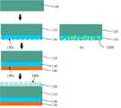
도 1은 본 발명의 실시 예에 따른 유기 발광소자용 기판을 나타낸 단면도.
도 2 및 도 3은 본 발명의 실시 예에 따른 유기 발광소자용 기판 제조방법을 실시 예에 따른 공정 순으로 나타낸 공정도.
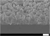
도 4 내지 도 7은 본 발명의 실시 예에 따른 유기 발광소자용 기판 제조방법을 통해 제조된 유기 발광소자용 기판의 단면을 주사전자현미경으로 촬영한 사진.1 is a cross-sectional view of a substrate for an organic light emitting device according to an embodiment of the present invention.
FIG. 2 and FIG. 3 are process diagrams showing a method of manufacturing a substrate for an organic light emitting diode according to an embodiment of the present invention, in the order of steps according to an embodiment.
4 to 7 are SEM photographs of a cross section of a substrate for an organic light emitting diode fabricated by the method for manufacturing a substrate for an organic light emitting diode according to an embodiment of the present invention.
이하에서는 첨부된 도면들을 참조하여 본 발명의 실시 예에 따른 유기 발광소자용 기판 및 그 제조방법에 대해 상세히 설명한다.Hereinafter, a substrate for an organic light emitting diode and a method of manufacturing the same according to an embodiment of the present invention will be described in detail with reference to the accompanying drawings.
아울러, 본 발명을 설명함에 있어서, 관련된 공지 기능 혹은 구성에 대한 구체적인 설명이 본 발명의 요지를 불필요하게 흐릴 수 있다고 판단된 경우 그 상세한 설명은 생략한다.
In the following description of the present invention, detailed description of known functions and configurations incorporated herein will be omitted when it may make the subject matter of the present invention rather unclear.
도 1에 도시한 바와 같이, 본 발명의 실시 예에 따른 유기 발광소자용 기판(100)은 유기 발광소자의 광추출 효율을 향상시키는 기판으로, 유기 발광소자에 사용되는 서로 대향되는 기판 중 유기 발광소자의 일면에 접합되는 기판이다. 그리고 이러한 유기 발광소자용 기판(100)은 유기 발광소자를 외부 환경으로부터 보호함과 동시에 유기 발광소자로부터 발생된 광을 외부로 방출시키는 통로 역할을 한다.As shown in FIG. 1, a
여기서, 도시하진 않았지만, 유기 발광소자는 본 발명의 실시 예에 따른 기판(100)과 이와 대향되는 봉지(encapsulation) 기판 사이에 배치되는 애노드, 유기 발광층 및 캐소드의 적층 구조로 이루어진다. 이때, 애노드는 본 발명의 실시 예에 따른 기판(100)에 포함되어 형성되는데, 이에 대해서는 하기에서 보다 상세히 설명하기로 한다. 캐소드는 전자 주입이 잘 일어나도록 일함수가 작은 Al, Al:Li 또는 Mg:Ag의 금속 박막으로 이루어져 있고, 전면 발광(top emission) 구조인 경우 유기 발광층에서 발광된 빛이 잘 투과될 수 있도록 Al, Al:Li 또는 Mg:Ag의 금속 박막의 반투명 전극(semitransparent electrode)과 인듐 주석산화물(indium tin oxide; ITO)과 같은 산화물 투명 전극(transparent electrode) 박막의 다층구조로 이루어질 수 있다. 그리고 유기 발광층은 애노드 상에 차례로 적층되는 정공 주입층, 정공 수송층, 발광층, 전자 수송층 및 전자 주입층을 포함하여 형성된다. 이러한 구조에 따라, 애노드와 캐소드 사이에 순방향 전압이 인가되면, 캐소드로부터 전자가 전자 주입층 및 전자 수송층을 통해 발광층으로 이동하게 되고, 애노드로부터 정공이 정공 주입층 및 정공 수송층을 통해 발광층으로 이동하게 된다. 그리고 발광층 내로 주입된 전자와 정공은 발광층에서 재결합하여 엑시톤(exciton)을 생성하고, 이러한 엑시톤이 여기상태(excited state)에서 기저상태(ground state)로 전이하면서 빛을 방출하게 되는데, 이때, 방출되는 빛의 밝기는 애노드와 캐소드 사이에 흐르는 전류량에 비례하게 된다.Here, although not shown, the organic light emitting device includes a stacked structure of an anode, an organic light emitting layer, and a cathode disposed between the
이와 같이, 유기 발광소자에 접합되는 본 발명의 실시 예에 따른 유기 발광소자용 기판(100)은 베이스 기판(110), 제1 금속 산화물 박막(120), 제2 금속 산화물 박막(130) 및 제3 금속 산화물 박막(140)을 포함하여 형성된다. 이때, 베이스 기판(110), 제1 금속 산화물 박막(120), 제2 금속 산화물 박막(130) 및 제3 금속 산화물 박막(140)은 상압화학기상증착 반응을 통한 인-라인(in-line) 공정으로 형성되어 하나의 패키지 형태를 이루게 된다.
The
베이스 기판(110)은 투명 기판으로, 광 투과율이 우수하고 기계적인 물성이 우수한 것이면 어느 것이든 제한되지 않는다. 예를 들어, 베이스 기판(110)은 열경화 또는 UV 경화가 가능한 유기필름인 폴리머 계열의 물질이나 화학강화유리인 소다라임유리(SiO2-CaO-Na2O) 또는 알루미노실리케이트유리(SiO2-Al2O3-Na2O)가 사용될 수 있으며, 이중 Na의 양은 용도에 따라 조절될 수 있다. 이때, 유기 발광소자가 조명용인 경우 소다라임유리가 사용될 수 있고, 유기 발광소자가 디스플레이용인 경우 알루미노실리케이트유리가 사용될 수 있다.The
본 발명의 실시 예에서, 베이스 기판(110)으로는 두께 1.5㎜ 이하의 박판 유리가 사용될 수 있는데, 이러한 박판 유리는 퓨전(fusion) 공법 또는 플로팅(floating) 공법을 통해 제조된다.
In the embodiment of the present invention, as the
제1 금속 산화물 박막(120)은 베이스 기판(110)의 일면에 코팅된다. 예를 들어, 제1 금속 산화물 박막(120)은 베이스 기판(110)의 상면(도면기준)에 코팅될 수 있다. 이때, 제1 금속 산화물 박막(120)은 베이스 기판(110)의 상면에 0.2 내지 5㎛ 두께로 코팅되는 것이 바람직하다. 이러한 제1 금속 산화물 박막(120)은 ZnO, SnO2, SiO2, Al2O3 및 TiO2로 이루어진 금속 산화물 물질군 중 하나 또는 둘 이상이 층을 이룬 적층구조로 이루어지거나 상기의 금속 산화물 물질군 중 둘 이상의 고용체로도 이루어질 수 있다.The first metal oxide
한편, 도 1, 도 4 및 도 5에 도시한 바와 같이, 제1 금속 산화물 박막(120)의 표면에는 제1 텍스처링(texturing)(120a)이 형성된다. 제1 텍스처링(120a)은 가시광선 영역의 빛을 산란시키는 역할을 하는 것으로, 막대, 하프 헥사곤 또는 육각 프리즘 형태로 형성되거나 랜덤한 형태로도 형성될 수 있다. 이러한 제1 텍스처링(120a)은 상압화학기상증착 반응을 통해 제1 금속 산화물 박막(120)을 증착시킬 때, 자연 발생적으로 형성될 수 있는데, 이에 대해서는 하기의 유기 발광소자용 기판 제조방법에서 보다 상세히 설명하기로 한다.Meanwhile, as shown in FIGS. 1, 4 and 5, a
도시한 바와 같이, 베이스 기판(110)의 상면에 형성되는 제1 금속 산화물 박막(120)은 유기 발광소자용 기판(100)의 최외각층으로, 유기 발광소자의 외부 광추출층으로서의 역할을 한다. 이와 같이, 제1 금속 산화물 박막(120)으로 이루어진 외부 광추출층은 60% 이상의 헤이즈(haze) 값을 가지고, 가시광선 영역에서 40% 이상의 투과율을 가지며, 1.4~3.0의 굴절률을 갖는다.
As shown in the figure, the first metal oxide
제2 금속 산화물 박막(130)은 베이스 기판(110)의 타면, 즉, 제1 산화물 박막(120)과 대응되는 베이스 기판(110)의 하면(도면기준)에 코팅된다. 이때, 제2 금속 산화물 박막(130)은 베이스 기판(110)의 하면에 0.2 내지 5㎛ 두께로 코팅되는 것이 바람직하다. 이러한 제2 금속 산화물 박막(130)은 제1 금속 산화물 박막(120)과 동일한 물질로 형성될 수 있다. 즉, 제2 금속 산화물 박막(130)은 ZnO, SnO2, SiO2, Al2O3 및 TiO2로 이루어진 금속 산화물 물질군 중 하나 또는 둘 이상이 층을 이룬 적층구조로 이루어지거나 상기의 금속 산화물 물질군 중 둘 이상의 고용체로도 이루어질 수 있다.The second metal oxide
한편, 도 1 및 도 6에 도시한 바와 같이, 제2 금속 산화물 박막(130)의 일면에는 빛을 산란시키는 제2 텍스처링(130a)이 막대, 막대의 한쪽이 하프 헥사곤, 또는 육각 프리즘 형태로 형성되거나 랜덤한 형태로 형성될 수 있다. 여기서, 제2 텍스처링(130a)이 형성되는 제2 금속 산화물 박막(130)의 일면은 제3 금속 산화물 박막(140)과의 경계면이다. 이러한 제2 텍스처링(130a)은 제1 텍스처링(120a)과 마찬가지로, 상압화학기상증착 반응을 통한 제2 금속 산화물 박막(130) 증착 시 자연 발생적으로 형성될 수 있다. 하지만, 제2 금속 산화물 박막(130)의 일면은 평탄면을 이룰 수도 있다.On the other hand, as shown in FIGS. 1 and 6, a
여기서, 제2 텍스처링(130a)의 표면, 즉, 제2 금속 산화물 박막(130)과 제3 금속 산화물 박막(140)의 경계면에는 평탄화층(미도시)이 형성될 수 있는데, 이는, 공정 상 후속으로 코팅되고, 유기 발광소자의 투명 전극 즉, 애노드 역할을 하는 제3 금속산화물 박막(140)의 평탄도를 확보하기 위함이다.Here, a planarization layer (not shown) may be formed on the surface of the
제2 금속 산화물 박막(130)은 ZnO, SnO2, SiO2, Al2O3 및 TiO2로 이루어진 금속 산화물 물질군 중 하나 또는 둘 이상이 층을 이룬 적층구조로 이루어지거나 상기의 금속 산화물 물질군 중 둘 이상의 고용체 이외에, 어느 한 물질은 매트릭스 형태를 취하고 다른 한 물질은 과포화되어 파티클(particle)로 석출된 형태를 취할 수 있다. 이 경우 파티클의 크기는 50㎚~400㎚이며 매트릭스는 이들 파티클을 수렴할 수 있는 최소 두께 이상이 필요하다.
The second metal oxide
도시한 바와 같이, 베이스 기판(110)의 하면에 형성되는 제2 금속 산화물 박막(130)은 유기 발광소자의 내부 광추출층으로서의 역할을 한다. 이와 같이, 제2 금속 산화물 박막(130)으로 이루어진 내부 광추출층은 5% 이상의 헤이즈 값을 가지고, 가시광선 영역에서 50% 이상의 투과율을 가지며, 1.4~3.0의 굴절률을 갖는다.
As shown in the figure, the second metal oxide
제3 금속 산화물 박막(140)은 제2 금속 산화물 박막(130)의 표면에 코팅된다. 이때, 제3 금속 산화물 박막(140)은 50 내지 2000㎚ 두께로 코팅되는 것이 바람직하다. 이러한 제3 금속 산화물 박막(140)은 ZnO, SnO2, SiO2, Al2O3 및 TiO2로 이루어진 금속 산화물 물질군 중 하나 또는 둘 이상이 층을 이룬 적층구조로 이루어지거나 상기의 금속 산화물 물질군 중 둘 이상의 고용체로도 이루어질 수 있다. 이때, 제3 금속 산화물 박막(140)은 유기 발광소자의 투명 전극 역할을 함에 따라, 전기적 특성을 나타내야 한다. 이를 위해, 상기의 금속 산화물 물질에 Ga, Al, F, Si, B를 포함하는 n형 도펀트 및 N을 포함하는 p형 도펀트 중 적어도 어느 하나가 포함될 수 있다. 이에 따라, 제3 금속 산화물 박막(140)은 15Ω/□ 이하의 면저항을 가진다.The third metal oxide
도 1 및 도 7에 도시한 바와 같이, 제3 금속 산화물 박막(140)은 평탄한 표면으로 형성된다. 이에 따라, 제3 금속 산화물 박막(140) 즉, 투명 전극은 10% 이하의 헤이즈 값을 갖는다. 그리고 이 투명 전극은 가시광선 영역에서 70% 이상의 투과율을 가지며, 1.7~3.0의 굴절률을 갖는다.
As shown in Figs. 1 and 7, the third metal oxide
이하, 본 발명의 실시 예에 따른 유기 발광소자용 기판 제조방법을 도 2 및 도 3을 참조하여 설명하기로 한다.Hereinafter, a method of manufacturing a substrate for an organic light emitting diode according to an embodiment of the present invention will be described with reference to FIGS. 2 and 3. FIG.
본 발명의 실시 예에 따른 유기 발광소자용 기판 제조방법은 상압화학기상증착 공정으로 베이스 기판의 일면 및 타면 각각에 적어도 하나의 금속 산화물 박막을 증착한다. 여기서, 금속 산화물 박막을 상압화학기상증착 반응으로 형성하면, 이의 표면에 증착 과정에서 자연 발생적으로 텍스처링이 형성된다. 즉, 상압화학기상증착 반응으로 금속 산화물 박막을 형성하면, 인위적으로 텍스처링을 형성하는 공정을 생략할 수 있어, 제조공정을 줄일 수 있고, 이에 따라, 생산성이 증가되어 대량 양산이 가능해진다.The method for manufacturing a substrate for an organic light emitting diode according to an embodiment of the present invention deposits at least one metal oxide thin film on one side and the other side of a base substrate by an atmospheric pressure chemical vapor deposition process. Here, when the metal oxide thin film is formed by an atmospheric pressure chemical vapor deposition reaction, texturing is formed spontaneously in the deposition process on the surface thereof. That is, when the metal oxide thin film is formed by the atmospheric pressure chemical vapor deposition reaction, the process of artificially forming the texturing can be omitted, and the manufacturing process can be reduced, thereby increasing the productivity and mass production.
이러한 상압화학기상증착 반응 공정은 먼저, 공정 챔버에 베이스 기판을 장입한 후 이를 소정의 온도로 가열한다. 그 다음 상압화학기상증착 반응을 위해 전구체 가스와 산화제 가스를 공정 챔버 내부로 분사한다. 이때, 전구체 가스와 산화제 가스가 공정 챔버 내부로 유입되기 전 미리 혼합되는 것을 방기 하기 위해 각각의 가스 공급 경로를 다르게 제어하는 것이 바람직하고, 화학 반응을 활성화시키기 위해 전구체 가스와 산화제 가스를 미리 가열하여 공급할 수 있다. 그리고 전구체 가스는 질소, 헬륨, 아르곤과 같은 비활성 가스로 이루어진 캐리어 가스에 의해 공정 챔버 내부로 운반될 수 있다.In this atmospheric chemical vapor deposition reaction process, first, a base substrate is loaded into a process chamber and then heated to a predetermined temperature. The precursor gas and oxidant gas are then injected into the process chamber for an atmospheric chemical vapor deposition reaction. At this time, it is preferable to control the respective gas supply paths differently in order to prevent premix gas and oxidizer gas from being mixed in advance before flowing into the process chamber. In order to activate the chemical reaction, the precursor gas and the oxidizer gas are heated Can supply. And the precursor gas may be carried into the process chamber by a carrier gas comprised of an inert gas such as nitrogen, helium, or argon.
여기서, 상압화학기상증착 반응 공정으로 금속 산화물 박막 증착 시 금속 산화물 박막의 표면에 생성되는 텍스처링의 형상 제어를 위해 상압화학기상증착 반응 공정 전 베이스 기판의 표면을 플라즈마 또는 화학처리하여 표면개질을 실시할 수 있다. 또한, 상압화학기상증착 반응 공정으로 금속 산화물 박막 증착 시 금속 산화물 박막의 표면에 생성되는 텍스처링의 형상 제어를 위해 상압화학기상증착 반응 공정 후 형성된 금속 산화물 박막의 표면을 플라즈마 또는 화학처리하여 표면개질을 실시할 수 있다.Here, in order to control the shape of the texturing formed on the surface of the metal oxide thin film during the metal oxide thin film deposition process by the atmospheric chemical vapor deposition reaction process, the surface of the base substrate is subjected to surface modification by plasma or chemical treatment before the atmospheric pressure chemical vapor deposition . In order to control the shape of the texturing on the surface of the metal oxide thin film during the metal oxide thin film deposition process by the atmospheric chemical vapor deposition reaction process, the surface of the metal oxide thin film formed after the atmospheric pressure chemical vapor deposition reaction process is plasma- .
도 2에 도시한 바와 같이, 이와 같은 상압화학기상증착 반응 공정을 이용하는 유기 발광소자용 기판 제조방법은, 먼저, 베이스 기판(110)을 준비한다. 이때, 베이스 기판(110)으로는 열경화 또는 UV 경화가 가능한 유기필름인 폴리머 계열의 물질이나 화학강화유리인 소다라임유리(SiO2-CaO-Na2O) 또는 알루미노실리케이트유리(SiO2-Al2O3-Na2O)를 사용할 수 있다.As shown in FIG. 2, in the method of manufacturing a substrate for an organic light emitting diode using the above atmospheric chemical vapor deposition reaction process, first, a
다음으로, 베이스 기판(110)의 상면에 유기 발광소자의 외부 광추출층으로 사용되는 제1 금속 산화물 박막(120)을 증착한다. 제1 금속 산화물 박막(120)을 증착시키기 위해, ZnO, SnO2, SiO2, Al2O3 및 TiO2로 이루어진 금속 산화물 물질군 중 하나 또는 둘 이상 또는 이들의 고용체를 사용할 수 있다. 상술한 바와 같이, 상압화학기상증착 반응을 통해, 제1 금속 산화물 박막(120)을 증착하면, 제1 금속 산화물 박막(120) 표면에 제1 텍스처링(120a)이 자연 발생적으로 형성된다.Next, a first metal oxide
다음으로, 베이스 기판(110)의 하면에 유기 발광소자의 내부 광추출층으로 사용되는 제2 금속 산화물 박막(130)을 증착한다. 제2 금속 산화물 박막(130)을 증착시키기 위해, ZnO, SnO2, SiO2, Al2O3 및 TiO2로 이루어진 금속 산화물 물질군 중 하나 또는 둘 이상 또는 이들의 고용체를 사용할 수 있다. 마찬가지로, 상압화학기상증착 반응을 통해, 제2 금속 산화물 박막(130)을 증착하면, 제2 금속 산화물 박막(130) 표면에 제2 텍스처링(130a)이 자연 발생적으로 형성된다. 이때, 후속 공정으로 코팅되는 제3 산화물 박막(140)의 평탄도를 확보하기 위해, 제2 텍스처링(130a)의 표면에 평탄화층을 형성하는 것이 바람직하다.Next, a second metal oxide
제2 금속 산화물 박막(130)은 ZnO, SnO2, SiO2, Al2O3 및 TiO2로 이루어진 금속 산화물 물질군 중 하나 또는 둘 이상이 층을 이룬 적층구조로 이루어지거나 상기의 금속 산화물 물질군 중 둘 이상의 고용체 이외에, 도 2의 (a)에 도시한 바와 같이, 어느 한 물질은 매트릭스 형태를 취하고 다른 한 물질은 과포화되어 파티클(particle)(130b)로 석출된 형태를 취할 수 있다. 이 경우 파티클(130b)의 크기는 50㎚~400㎚이며 매트릭스는 이들 파티클(130b)을 수렴할 수 있는 최소 두께 이상이 필요하다.
The second metal oxide
마지막으로, 제2 금속 산화물 박막(130) 표면에 유기 발광소자의 투명 전극으로 사용되는 제3 금속 산화물 박막(140)을 증착한다. 제3 금속 산화물 박막(140)을 증착시키기 위해, ZnO, SnO2, SiO2, Al2O3 및 TiO2로 이루어진 금속 산화물 물질군 중 하나 또는 둘 이상 또는 이들의 고용체를 사용할 수 있다. 아울러, 제3 금속 산화물 박막(140)의 전도성 부여를 위해, 3 금속 산화물 박막(140)에 Ga, Al, F, Si, B를 포함하는 n형 도펀트 및 N을 포함하는 p형 도펀트 중 적어도 어느 하나를 도핑시킬 수 있다.Finally, a third metal oxide
이와 같이, 제3 금속 산화물 박막(140)을 증착하면, 본 발명의 실시 예에 따른 유기 발광소자용 기판 제조가 완료된다. 본 발명의 실시 예에 따른 유기 발광소자용 기판 제조방법은 상압화학기상증착 공정을 통한 인-라인(in-line) 공정으로 상기의 공정을 진행함으로써, 종래 각기 다른 공정으로 진행되던 박막 증착 공정을 단순화, 간소화시킬 수 있고, 이에 따라 제조 비용도 절감할 수 있으며, 기능적인 매칭성까지 향상시킬 수 있다.When the third metal oxide
여기서, 도 3에 도시한 바와 같이, 제1 금속 산화물 박막(120)은 제2 및 제3 금속 산화물 박막(130, 140)을 먼저 증착한 다음 증착할 수도 있다.
Here, as shown in FIG. 3, the first metal oxide
이상과 같이 본 발명은 비록 한정된 실시 예와 도면에 의해 설명되었으나, 본 발명은 상기의 실시 예에 한정되는 것은 아니며, 본 발명이 속하는 분야에서 통상의 지식을 가진 자라면 이러한 기재로부터 다양한 수정 및 변형이 가능하다.While the invention has been shown and described with reference to certain preferred embodiments thereof, it will be understood by those of ordinary skill in the art that various changes in form and details may be made therein without departing from the spirit and scope of the invention as defined by the appended claims. This is possible.
그러므로 본 발명의 범위는 설명된 실시 예에 국한되어 정해져서는 아니 되며, 후술하는 특허청구범위뿐만 아니라 특허청구범위와 균등한 것들에 의해 정해져야 한다.Therefore, the scope of the present invention should not be limited by the described embodiments, but should be determined by the scope of the appended claims as well as the appended claims.
100: 유기 발광소자용 기판 110: 베이스 기판
120: 제1 금속 산화물 박막 120a: 제1 텍스처링
130: 제2 금속 산화물 박막 130a: 제2 텍스처링
130b: 파티클 140: 제3 금속 산화물 박막100: substrate for organic light emitting device 110: base substrate
120: first metal oxide
130: second metal oxide
130b: Particle 140: Third metal oxide thin film
Claims (17)
Translated fromKorean상기 베이스 기판의 일면에 코팅되고, 표면에 제1 텍스처링이 형성되는 제1 금속 산화물 박막;
상기 베이스 기판의 타면에 코팅되는 제2 금속 산화물 박막;
상기 제2 금속 산화물 박막의 표면에 코팅되는 제3 금속 산화물 박막;
을 포함하고,
상기 제2 금속 산화물 박막은 ZnO, SnO2, SiO2, Al2O3 및 TiO2로 이루어진 금속 산화물 물질군 중 선택된 둘 이상의 금속 산화물로 이루어지되, 선택된 둘 이상의 금속 산화물 중 한 물질은 매트릭스를 이루고, 나머지 물질은 상기 매트릭스 내에 과포화되어 석출된 파티클을 이루며,
상기 제3 금속 산화물 박막이 코팅되는 상기 제2 금속 산화물 박막의 일면에는 제2 텍스처링이 형성되는 것을 특징으로 하는 유기 발광소자용 기판.
A base substrate;
A first metal oxide thin film coated on one surface of the base substrate and having a first texturing formed on a surface thereof;
A second metal oxide thin film coated on the other surface of the base substrate;
A third metal oxide thin film coated on a surface of the second metal oxide thin film;
/ RTI >
Wherein the second metal oxide thin film is formed of at least two metal oxides selected from the group consisting of ZnO, SnO2 , SiO2 , Al2 O3, and TiO2 , wherein one of the two or more selected metal oxides forms a matrix , The remaining material is supersaturated in the matrix to form precipitated particles,
Wherein a second texturing is formed on one surface of the second metal oxide thin film on which the third metal oxide thin film is coated.
상기 제1 금속 산화물 박막은 유기 발광소자의 외부 광추출층이고, 상기 제2 금속 산화물 박막은 상기 유기 발광소자의 내부 광추출층이며, 상기 제3 금속 산화물 박막은 상기 유기 발광소자의 투명 전극인 것을 특징으로 하는 유기 발광소자용 기판.
The method according to claim 1,
Wherein the first metal oxide thin film is an external light extracting layer of the organic light emitting device, the second metal oxide thin film is an internal light extracting layer of the organic light emitting device, and the third metal oxide thin film is a transparent electrode of the organic light emitting device Wherein the organic light-emitting device comprises: a substrate;
상기 제2 금속 산화물 박막과 상기 제3 금속 산화물 박막 사이에는 평탄화층이 형성되는 것을 특징으로 하는 유기 발광소자용 기판.
The method according to claim 1,
And a planarization layer is formed between the second metal oxide thin film and the third metal oxide thin film.
상기 제1 및 제3 금속 산화물 박막은 ZnO, SnO2, SiO2, Al2O3 및 TiO2로 이루어진 금속 산화물 물질군 중 둘 이상의 고용체 또는 적층구조로 이루어진 것을 특징으로 하는 유기 발광소자용 기판.
The method according to claim 1,
Wherein the first and third metal oxide thin films are formed of at least two solid solution or laminated structures among a group of metal oxide materials consisting of ZnO, SnO2 , SiO2 , Al2 O3 and TiO2 .
상기 외부 광추출층의 헤이즈 값은 60% 이상, 상기 내부 광추출층의 헤이즈 값은 5% 이상, 상기 투명 전극의 헤이즈 값은 10% 이하인 것을 특징으로 하는 유기 발광소자용 기판.
3. The method of claim 2,
Wherein a haze value of the external light extracting layer is 60% or more, a haze value of the internal light extracting layer is 5% or more, and a haze value of the transparent electrode is 10% or less.
상기 투명 전극의 면저항은 15Ω/□ 이하인 것을 특징으로 하는 유기 발광소자용 기판.
3. The method of claim 2,
And the sheet resistance of the transparent electrode is 15? /? Or less.
가시광선 영역에서, 상기 외부 광추출층의 투과율은 40% 이상, 상기 내부 광추출층의 투과율은 50% 이상, 상기 투명 전극의 투과율은 70% 이상인 것을 특징으로 하는 유기 발광소자용 기판.
3. The method of claim 2,
Wherein the transmittance of the external light extracting layer is 40% or more, the transmittance of the internal light extracting layer is 50% or more, and the transmittance of the transparent electrode is 70% or more in the visible light region.
상기 외부 광추출층의 굴절률은 1.4~3.0, 상기 내부 광추출층의 굴절률은 1.4~3.0, 상기 투명 전극의 굴절률은 1.7~3.0인 것을 특징으로 하는 유기 발광소자용 기판.
3. The method of claim 2,
Wherein the refractive index of the external light extracting layer is 1.4 to 3.0, the refractive index of the internal light extracting layer is 1.4 to 3.0, and the refractive index of the transparent electrode is 1.7 to 3.0.
상기 베이스 기판의 일면에 유기 발광소자의 외부 광추출층으로 사용되는 제1 금속 산화물 박막을 증착하는 제1 단계;
상기 베이스 기판의 타면에 상기 유기 발광소자의 내부 광추출층으로 사용되는 제2 금속 산화물 박막을 증착하는 제2 단계; 및
상기 제2 금속 산화물 박막 표면에 상기 유기 발광소자의 투명 전극으로 사용되는 제3 금속 산화물 박막을 증착하는 제3 단계;
를 포함하고,
상기 제1 내지 제3 금속 산화물 박막을 이루는 물질로 ZnO, SnO2, SiO2, Al2O3 및 TiO2로 이루어진 금속 산화물 물질군 중 둘 이상 또는 이들의 고용체를 사용하여, 상기 제1 단계 내지 제3 단계를 인-라인(in-line) 공정으로 진행하며,
상기 제1 금속 산화물 박막 및 상기 제2 금속 산화물 박막 표면에는 증착 과정에서 텍스처링이 자연 발생적으로 형성되되,
상기 제1 단계 내지 제3 단계 진행 전, 상기 베이스 기판의 표면을 플라즈마 또는 화학처리하여 표면개질하거나 상기 제1 금속 산화물 박막 및 상기 제2 금속 산화물 박막 증착 후 상기 제1 금속 산화물 박막 및 상기 제2 금속 산화물 박막 표면을 플라즈마 또는 화학처리하여 표면개질함으로서 상기 텍스처링의 형상을 제어하는 것을 특징으로 하는 유기 발광소자용 기판 제조방법.
Depositing at least one metal oxide thin film on one side and the other side of the base substrate by an atmospheric chemical vapor deposition process,
A first step of depositing a first metal oxide thin film used as an external light extracting layer of an organic light emitting device on one surface of the base substrate;
A second step of depositing a second metal oxide thin film used as an internal light extracting layer of the organic light emitting device on the other surface of the base substrate; And
A third step of depositing a third metal oxide thin film used as a transparent electrode of the organic light emitting diode on the surface of the second metal oxide thin film;
Lt; / RTI >
Wherein the first to third metal oxide thin films are formed by using two or more metal oxide material materials or a solid solution thereof composed of ZnO, SnO2 , SiO2 , Al2 O3, and TiO2 , The third step proceeds to an in-line process,
The surface of the first metal oxide thin film and the surface of the second metal oxide thin film are spontaneously formed in the deposition process,
The surface of the base substrate may be surface-modified by plasma or chemical treatment before proceeding to the first to third steps or after the first metal oxide thin film and the second metal oxide thin film are deposited, Wherein the shape of the texturing is controlled by surface-modifying the surface of the metal oxide thin film by plasma or chemical treatment.
상기 제2 단계와 상기 제3 단계 진행 후 상기 제1 단계를 진행하는 것을 특징으로 하는 유기 발광소자용 기판 제조방법.
12. The method of claim 11,
Wherein the first step is performed after the second step and the third step are performed.
상기 제2 단계와 상기 제3 단계 사이에 상기 제2 금속 산화물 박막 상에 평탄화층을 형성하는 단계를 더 포함하는 것을 특징으로 하는 유기 발광소자용 기판 제조방법.
14. The method of claim 13,
And forming a planarization layer on the second metal oxide thin film between the second step and the third step.
상기 제3 단계에서는 상기 제3 금속 산화물 박막에 Ga, Al, F, Si, B를 포함하는 n형 도펀트 및 N을 포함하는 p형 도펀트 중 적어도 어느 하나를 도핑하는 것을 특징으로 하는 유기 발광소자용 기판 제조방법.
15. The method of claim 14,
Wherein the third metal oxide thin film is doped with at least one of an n-type dopant including Ga, Al, F, Si, and B and a p-type dopant including N in the third step ≪ / RTI >
Priority Applications (4)
| Application Number | Priority Date | Filing Date | Title |
|---|---|---|---|
| KR1020120067315AKR101654360B1 (en) | 2012-06-22 | 2012-06-22 | Substrate for oled and method for fabricating thereof |
| US13/921,294US20130341605A1 (en) | 2012-06-22 | 2013-06-19 | Substrate For OLED And Method Of Manufacturing The Same |
| EP13173163.0AEP2704226A3 (en) | 2012-06-22 | 2013-06-21 | Substrate for oled and method of manufacturing the same |
| CN201310252902.XACN103515541A (en) | 2012-06-22 | 2013-06-24 | Substrate for OLED and method of manufacturing the same |
Applications Claiming Priority (1)
| Application Number | Priority Date | Filing Date | Title |
|---|---|---|---|
| KR1020120067315AKR101654360B1 (en) | 2012-06-22 | 2012-06-22 | Substrate for oled and method for fabricating thereof |
Publications (2)
| Publication Number | Publication Date |
|---|---|
| KR20140000426A KR20140000426A (en) | 2014-01-03 |
| KR101654360B1true KR101654360B1 (en) | 2016-09-05 |
Family
ID=48651918
Family Applications (1)
| Application Number | Title | Priority Date | Filing Date |
|---|---|---|---|
| KR1020120067315AActiveKR101654360B1 (en) | 2012-06-22 | 2012-06-22 | Substrate for oled and method for fabricating thereof |
Country Status (4)
| Country | Link |
|---|---|
| US (1) | US20130341605A1 (en) |
| EP (1) | EP2704226A3 (en) |
| KR (1) | KR101654360B1 (en) |
| CN (1) | CN103515541A (en) |
Families Citing this family (10)
| Publication number | Priority date | Publication date | Assignee | Title |
|---|---|---|---|---|
| TWI495175B (en)* | 2012-11-16 | 2015-08-01 | Au Optronics Corp | Organic electroluminescent element |
| KR101632614B1 (en) | 2014-12-24 | 2016-06-22 | 코닝정밀소재 주식회사 | Method of fabricating light extraction substrate, light extraction substrate for oled and oled including the same |
| KR101762648B1 (en)* | 2014-12-29 | 2017-07-31 | 코닝정밀소재 주식회사 | Method of fabricating light extraction substrate, light extraction substrate for oled and oled including the same |
| CN105280838B (en)* | 2015-09-22 | 2017-08-25 | 深圳市华星光电技术有限公司 | A kind of OLED luminescent devices and display device |
| CN105244453B (en)* | 2015-09-22 | 2017-08-25 | 深圳市华星光电技术有限公司 | A kind of organic luminescent device |
| JP6871705B2 (en)* | 2016-09-29 | 2021-05-12 | デクセリアルズ株式会社 | Optical body, manufacturing method of optical body, and light emitting device |
| TWI605288B (en) | 2017-01-16 | 2017-11-11 | 友達光電股份有限公司 | Pixel structure and display panel having the pixel structure |
| CN106981581A (en)* | 2017-02-08 | 2017-07-25 | 广东工业大学 | A kind of organic electroluminescence device for improving light extraction efficiency |
| WO2024191121A1 (en)* | 2023-03-10 | 2024-09-19 | 고려대학교 산학협력단 | Transparent metal oxide substrate and manufacturing method thereof |
| KR102831416B1 (en)* | 2023-03-10 | 2025-07-08 | 고려대학교 산학협력단 | Metal oxide transparent substrate and manufacturing method thereof |
Family Cites Families (18)
| Publication number | Priority date | Publication date | Assignee | Title |
|---|---|---|---|---|
| JPWO2003026356A1 (en)* | 2001-09-12 | 2005-01-06 | 日産化学工業株式会社 | Transparent substrate for organic electroluminescence device and device |
| EP1443527A4 (en)* | 2001-10-19 | 2007-09-12 | Asahi Glass Co Ltd | TRANSPARENT CONDUCTIVE OXIDE LAYER SUBSTRATE, PROCESS FOR PRODUCING THE SAME, AND PHOTOELECTRIC CONVERSION ELEMENT |
| US7151532B2 (en)* | 2002-08-09 | 2006-12-19 | 3M Innovative Properties Company | Multifunctional multilayer optical film |
| JP2005038681A (en)* | 2003-07-18 | 2005-02-10 | Toyota Industries Corp | Transparent substrate for forming bottom emission type light-emitting element, and light-emitting device using same |
| US20060040067A1 (en)* | 2004-08-23 | 2006-02-23 | Thomas Culp | Discharge-enhanced atmospheric pressure chemical vapor deposition |
| JP2006066264A (en)* | 2004-08-27 | 2006-03-09 | Fuji Photo Film Co Ltd | Organic electroluminescent element, method for preparing substrate with prism structure, and method for manufacturing organic electroluminescent element using the substrate |
| EP2090139A2 (en)* | 2006-11-17 | 2009-08-19 | Saint-Gobain Glass France | Electrode for an organic light-emitting device, acid etching thereof, and also organic light-emitting device incorporating it |
| US7911133B2 (en)* | 2007-05-10 | 2011-03-22 | Global Oled Technology Llc | Electroluminescent device having improved light output |
| KR101548025B1 (en)* | 2007-07-27 | 2015-08-27 | 아사히 가라스 가부시키가이샤 | Translucent substrate, method for manufacturing the translucent substrate, organic led element and method for manufacturing the organic led element |
| JP5010556B2 (en)* | 2007-08-27 | 2012-08-29 | パナソニック株式会社 | Organic EL light emitting device |
| KR20100043517A (en)* | 2008-10-20 | 2010-04-29 | 엘지디스플레이 주식회사 | Method for manufacturing metal oxide electrode and organci light emitting display using the same |
| JP2012521078A (en)* | 2009-03-17 | 2012-09-10 | アイメック | Plasma texture method |
| KR20100130019A (en)* | 2009-06-02 | 2010-12-10 | 삼성전자주식회사 | Manufacturing method of metal oxide layer, thin film transistor substrate manufactured using said method and manufacturing method thereof |
| US10581020B2 (en)* | 2011-02-08 | 2020-03-03 | Vitro Flat Glass Llc | Light extracting substrate for organic light emitting diode |
| KR101163647B1 (en)* | 2010-05-27 | 2012-07-09 | 순천대학교 산학협력단 | TCO layer and method for fabricating the same |
| EP2697840A4 (en)* | 2011-04-12 | 2014-11-05 | Arkema Inc | INTERNAL OPTICAL EXTRACTION LAYER FOR OLED DEVICES |
| EP2518789B1 (en)* | 2011-04-18 | 2016-04-13 | Corning Precision Materials Co., Ltd. | Method of manufacturing a light extraction substrate for an electroluminescent device |
| CN102299266A (en)* | 2011-09-15 | 2011-12-28 | 四川虹视显示技术有限公司 | Substrate of organic light-emitting diode (OLED) and manufacturing method for substrate |
- 2012
- 2012-06-22KRKR1020120067315Apatent/KR101654360B1/enactiveActive
- 2013
- 2013-06-19USUS13/921,294patent/US20130341605A1/ennot_activeAbandoned
- 2013-06-21EPEP13173163.0Apatent/EP2704226A3/ennot_activeWithdrawn
- 2013-06-24CNCN201310252902.XApatent/CN103515541A/enactivePending
Also Published As
| Publication number | Publication date |
|---|---|
| CN103515541A (en) | 2014-01-15 |
| US20130341605A1 (en) | 2013-12-26 |
| EP2704226A3 (en) | 2017-03-01 |
| KR20140000426A (en) | 2014-01-03 |
| EP2704226A2 (en) | 2014-03-05 |
Similar Documents
| Publication | Publication Date | Title |
|---|---|---|
| KR101654360B1 (en) | Substrate for oled and method for fabricating thereof | |
| WO2018113019A1 (en) | Oled display panel and manufacturing method therefor | |
| US20090152533A1 (en) | Increasing the external efficiency of light emitting diodes | |
| KR20050122967A (en) | An organic electroluminescent display device and method for preparing the same | |
| TW202125868A (en) | Organic light-emitting diode (oled) display devices with uv-cured filler | |
| CN107634082B (en) | Active light emitting display panel and manufacturing method thereof | |
| KR101608273B1 (en) | Method of fabricating light extraction substrate for oled, light extraction substrate for oled and oled including the same | |
| KR20140046728A (en) | Metallic oxide thin film substrate, method of fabricating thereof and oled including the same | |
| US9464351B2 (en) | Method of fabricating light-scattering substrate | |
| KR101650541B1 (en) | Flexible substrate and method of fabricating thereof | |
| JP6340674B2 (en) | Light extraction substrate for organic light emitting device, manufacturing method thereof, and organic light emitting device including the same | |
| US9711762B2 (en) | Substrate for organic light-emitting diode, method for manufacturing same, and organic light-emitting diode comprising same | |
| CN105518896A (en) | Method for fabricating ultra-thin organic light-emitting device | |
| KR101421026B1 (en) | Light extraction layer substrate for oled and method of fabricating thereof | |
| KR100843551B1 (en) | Organic electroluminescent display device comprising light diffusing layer and manufacturing method thereof | |
| KR101299534B1 (en) | Light extraction layer for oled and manufacturing method thereof | |
| KR101466833B1 (en) | Light extraction substrate for oled, method of fabricating thereof and oled including the same | |
| KR101570968B1 (en) | Substrate for oled, method for fabricating thereof and oled having the same | |
| KR101265656B1 (en) | Light extraction layer for oled and manufacturing method thereof | |
| KR101604495B1 (en) | Organic light emitting diode display device and method of manufacturing the same | |
| CN110993822B (en) | A display panel, its manufacturing method and display device | |
| KR20130070313A (en) | Organic electroluminescent device | |
| KR101470293B1 (en) | Method of fabricating light extraction substrate for oled | |
| KR101436548B1 (en) | Light extraction substrate, and method of fabricating light extraction substrate for oled | |
| CN203746913U (en) | Organic Light Emitting Diode Structure |
Legal Events
| Date | Code | Title | Description |
|---|---|---|---|
| PA0109 | Patent application | Patent event code:PA01091R01D Comment text:Patent Application Patent event date:20120622 | |
| PG1501 | Laying open of application | ||
| A201 | Request for examination | ||
| PA0201 | Request for examination | Patent event code:PA02012R01D Patent event date:20141203 Comment text:Request for Examination of Application Patent event code:PA02011R01I Patent event date:20120622 Comment text:Patent Application | |
| E902 | Notification of reason for refusal | ||
| PE0902 | Notice of grounds for rejection | Comment text:Notification of reason for refusal Patent event date:20150821 Patent event code:PE09021S01D | |
| E90F | Notification of reason for final refusal | ||
| PE0902 | Notice of grounds for rejection | Comment text:Final Notice of Reason for Refusal Patent event date:20160224 Patent event code:PE09021S02D | |
| E701 | Decision to grant or registration of patent right | ||
| PE0701 | Decision of registration | Patent event code:PE07011S01D Comment text:Decision to Grant Registration Patent event date:20160823 | |
| GRNT | Written decision to grant | ||
| PR0701 | Registration of establishment | Comment text:Registration of Establishment Patent event date:20160830 Patent event code:PR07011E01D | |
| PR1002 | Payment of registration fee | Payment date:20160830 End annual number:3 Start annual number:1 | |
| PG1601 | Publication of registration | ||
| FPAY | Annual fee payment | Payment date:20190701 Year of fee payment:4 | |
| PR1001 | Payment of annual fee | Payment date:20190701 Start annual number:4 End annual number:4 | |
| PR1001 | Payment of annual fee | Payment date:20200617 Start annual number:5 End annual number:5 | |
| PR1001 | Payment of annual fee | Payment date:20210624 Start annual number:6 End annual number:6 | |
| PR1001 | Payment of annual fee | Payment date:20220620 Start annual number:7 End annual number:7 | |
| PR1001 | Payment of annual fee | Payment date:20230628 Start annual number:8 End annual number:8 | |
| PR1001 | Payment of annual fee | Payment date:20240624 Start annual number:9 End annual number:9 | |
| PR1001 | Payment of annual fee | Payment date:20250623 Start annual number:10 End annual number:10 |