KR101645404B1 - Organic Light Emitting Display - Google Patents
Organic Light Emitting DisplayDownload PDFInfo
- Publication number
- KR101645404B1 KR101645404B1KR1020100064850AKR20100064850AKR101645404B1KR 101645404 B1KR101645404 B1KR 101645404B1KR 1020100064850 AKR1020100064850 AKR 1020100064850AKR 20100064850 AKR20100064850 AKR 20100064850AKR 101645404 B1KR101645404 B1KR 101645404B1
- Authority
- KR
- South Korea
- Prior art keywords
- transistor
- pixel
- electrode
- power source
- light emitting
- Prior art date
- Legal status (The legal status is an assumption and is not a legal conclusion. Google has not performed a legal analysis and makes no representation as to the accuracy of the status listed.)
- Active
Links
- 239000003990capacitorSubstances0.000claimsdescription22
- 238000000034methodMethods0.000description33
- 238000010586diagramMethods0.000description11
- 239000011521glassSubstances0.000description10
- 230000007547defectEffects0.000description3
- 238000003780insertionMethods0.000description3
- 230000037431insertionEffects0.000description3
- 239000011159matrix materialSubstances0.000description3
- 238000004519manufacturing processMethods0.000description2
- 230000001808coupling effectEffects0.000description1
- 239000004973liquid crystal related substanceSubstances0.000description1
- 230000000750progressive effectEffects0.000description1
- 230000006798recombinationEffects0.000description1
- 238000005215recombinationMethods0.000description1
- 238000002834transmittanceMethods0.000description1
Images


Classifications
- G—PHYSICS
- G09—EDUCATION; CRYPTOGRAPHY; DISPLAY; ADVERTISING; SEALS
- G09G—ARRANGEMENTS OR CIRCUITS FOR CONTROL OF INDICATING DEVICES USING STATIC MEANS TO PRESENT VARIABLE INFORMATION
- G09G3/00—Control arrangements or circuits, of interest only in connection with visual indicators other than cathode-ray tubes
- G09G3/20—Control arrangements or circuits, of interest only in connection with visual indicators other than cathode-ray tubes for presentation of an assembly of a number of characters, e.g. a page, by composing the assembly by combination of individual elements arranged in a matrix no fixed position being assigned to or needed to be assigned to the individual characters or partial characters
- G09G3/22—Control arrangements or circuits, of interest only in connection with visual indicators other than cathode-ray tubes for presentation of an assembly of a number of characters, e.g. a page, by composing the assembly by combination of individual elements arranged in a matrix no fixed position being assigned to or needed to be assigned to the individual characters or partial characters using controlled light sources
- G09G3/30—Control arrangements or circuits, of interest only in connection with visual indicators other than cathode-ray tubes for presentation of an assembly of a number of characters, e.g. a page, by composing the assembly by combination of individual elements arranged in a matrix no fixed position being assigned to or needed to be assigned to the individual characters or partial characters using controlled light sources using electroluminescent panels
- G09G3/32—Control arrangements or circuits, of interest only in connection with visual indicators other than cathode-ray tubes for presentation of an assembly of a number of characters, e.g. a page, by composing the assembly by combination of individual elements arranged in a matrix no fixed position being assigned to or needed to be assigned to the individual characters or partial characters using controlled light sources using electroluminescent panels semiconductive, e.g. using light-emitting diodes [LED]
- G09G3/3208—Control arrangements or circuits, of interest only in connection with visual indicators other than cathode-ray tubes for presentation of an assembly of a number of characters, e.g. a page, by composing the assembly by combination of individual elements arranged in a matrix no fixed position being assigned to or needed to be assigned to the individual characters or partial characters using controlled light sources using electroluminescent panels semiconductive, e.g. using light-emitting diodes [LED] organic, e.g. using organic light-emitting diodes [OLED]
- G09G3/3225—Control arrangements or circuits, of interest only in connection with visual indicators other than cathode-ray tubes for presentation of an assembly of a number of characters, e.g. a page, by composing the assembly by combination of individual elements arranged in a matrix no fixed position being assigned to or needed to be assigned to the individual characters or partial characters using controlled light sources using electroluminescent panels semiconductive, e.g. using light-emitting diodes [LED] organic, e.g. using organic light-emitting diodes [OLED] using an active matrix
- G09G3/3233—Control arrangements or circuits, of interest only in connection with visual indicators other than cathode-ray tubes for presentation of an assembly of a number of characters, e.g. a page, by composing the assembly by combination of individual elements arranged in a matrix no fixed position being assigned to or needed to be assigned to the individual characters or partial characters using controlled light sources using electroluminescent panels semiconductive, e.g. using light-emitting diodes [LED] organic, e.g. using organic light-emitting diodes [OLED] using an active matrix with pixel circuitry controlling the current through the light-emitting element
- G—PHYSICS
- G09—EDUCATION; CRYPTOGRAPHY; DISPLAY; ADVERTISING; SEALS
- G09G—ARRANGEMENTS OR CIRCUITS FOR CONTROL OF INDICATING DEVICES USING STATIC MEANS TO PRESENT VARIABLE INFORMATION
- G09G2300/00—Aspects of the constitution of display devices
- G09G2300/08—Active matrix structure, i.e. with use of active elements, inclusive of non-linear two terminal elements, in the pixels together with light emitting or modulating elements
- G09G2300/0809—Several active elements per pixel in active matrix panels
- G09G2300/0819—Several active elements per pixel in active matrix panels used for counteracting undesired variations, e.g. feedback or autozeroing
- G—PHYSICS
- G09—EDUCATION; CRYPTOGRAPHY; DISPLAY; ADVERTISING; SEALS
- G09G—ARRANGEMENTS OR CIRCUITS FOR CONTROL OF INDICATING DEVICES USING STATIC MEANS TO PRESENT VARIABLE INFORMATION
- G09G2300/00—Aspects of the constitution of display devices
- G09G2300/08—Active matrix structure, i.e. with use of active elements, inclusive of non-linear two terminal elements, in the pixels together with light emitting or modulating elements
- G09G2300/0809—Several active elements per pixel in active matrix panels
- G09G2300/0842—Several active elements per pixel in active matrix panels forming a memory circuit, e.g. a dynamic memory with one capacitor
- G09G2300/0852—Several active elements per pixel in active matrix panels forming a memory circuit, e.g. a dynamic memory with one capacitor being a dynamic memory with more than one capacitor
- G—PHYSICS
- G09—EDUCATION; CRYPTOGRAPHY; DISPLAY; ADVERTISING; SEALS
- G09G—ARRANGEMENTS OR CIRCUITS FOR CONTROL OF INDICATING DEVICES USING STATIC MEANS TO PRESENT VARIABLE INFORMATION
- G09G2300/00—Aspects of the constitution of display devices
- G09G2300/08—Active matrix structure, i.e. with use of active elements, inclusive of non-linear two terminal elements, in the pixels together with light emitting or modulating elements
- G09G2300/0809—Several active elements per pixel in active matrix panels
- G09G2300/0842—Several active elements per pixel in active matrix panels forming a memory circuit, e.g. a dynamic memory with one capacitor
- G09G2300/0861—Several active elements per pixel in active matrix panels forming a memory circuit, e.g. a dynamic memory with one capacitor with additional control of the display period without amending the charge stored in a pixel memory, e.g. by means of additional select electrodes
- G09G2300/0866—Several active elements per pixel in active matrix panels forming a memory circuit, e.g. a dynamic memory with one capacitor with additional control of the display period without amending the charge stored in a pixel memory, e.g. by means of additional select electrodes by means of changes in the pixel supply voltage
- G—PHYSICS
- G09—EDUCATION; CRYPTOGRAPHY; DISPLAY; ADVERTISING; SEALS
- G09G—ARRANGEMENTS OR CIRCUITS FOR CONTROL OF INDICATING DEVICES USING STATIC MEANS TO PRESENT VARIABLE INFORMATION
- G09G2310/00—Command of the display device
- G09G2310/02—Addressing, scanning or driving the display screen or processing steps related thereto
- G09G2310/0243—Details of the generation of driving signals
- G09G2310/0248—Precharge or discharge of column electrodes before or after applying exact column voltages
- G—PHYSICS
- G09—EDUCATION; CRYPTOGRAPHY; DISPLAY; ADVERTISING; SEALS
- G09G—ARRANGEMENTS OR CIRCUITS FOR CONTROL OF INDICATING DEVICES USING STATIC MEANS TO PRESENT VARIABLE INFORMATION
- G09G3/00—Control arrangements or circuits, of interest only in connection with visual indicators other than cathode-ray tubes
- G09G3/001—Control arrangements or circuits, of interest only in connection with visual indicators other than cathode-ray tubes using specific devices not provided for in groups G09G3/02 - G09G3/36, e.g. using an intermediate record carrier such as a film slide; Projection systems; Display of non-alphanumerical information, solely or in combination with alphanumerical information, e.g. digital display on projected diapositive as background
- G09G3/003—Control arrangements or circuits, of interest only in connection with visual indicators other than cathode-ray tubes using specific devices not provided for in groups G09G3/02 - G09G3/36, e.g. using an intermediate record carrier such as a film slide; Projection systems; Display of non-alphanumerical information, solely or in combination with alphanumerical information, e.g. digital display on projected diapositive as background to produce spatial visual effects
Landscapes
- Engineering & Computer Science (AREA)
- Physics & Mathematics (AREA)
- Computer Hardware Design (AREA)
- General Physics & Mathematics (AREA)
- Theoretical Computer Science (AREA)
- Control Of El Displays (AREA)
- Electroluminescent Light Sources (AREA)
- Control Of Indicators Other Than Cathode Ray Tubes (AREA)
Abstract
Translated fromKoreanDescription
Translated fromKorean본 발명은 유기 전계발광 표시장치에 관한 것으로, 특히 동시 발광 방식으로 구동되는 유기 전계발광 표시장치에 관한 것이다.BACKGROUND OF THE INVENTION 1. Field of the Invention [0001] The present invention relates to an organic light emitting display device, and more particularly to an organic light emitting display device driven by a simultaneous light emitting method.
최근, 음극선관(Cathode Ray Tube)의 단점인 무게와 부피를 줄일 수 있는 각종 평판 표시장치들이 개발되고 있다. 평판 표시장치로는 액정 표시장치(Liquid Crystal Display: LCD), 전계방출 표시장치(Field Emission Display: FED), 플라즈마 표시패널(Plasma Display Panel: PDP) 및 유기 전계발광 표시장치(Organic Light Emitting Display: OLED) 등이 있다.2. Description of the Related Art Recently, various flat panel display devices capable of reducing weight and volume, which are disadvantages of cathode ray tubes (CRTs), have been developed. Examples of the flat panel display include a liquid crystal display (LCD), a field emission display (FED), a plasma display panel (PDP), and an organic light emitting display OLED).
평판 표시장치 중 유기 전계발광 표시장치는 전자와 정공의 재결합에 의하여 빛을 발생하는 유기 발광 다이오드를 이용하여 영상을 표시하는 것으로, 이는 빠른 응답속도를 가짐과 동시에 낮은 소비전력으로 구동되는 장점이 있다.Among the flat panel display devices, the organic light emitting display device displays an image using an organic light emitting diode that generates light by recombination of electrons and holes, and has advantages of fast response speed and low power consumption .
통상적으로, 유기전계발광 표시장치(OLED)는 유기발광소자를 구동하는 방식에 따라 패시브 매트릭스형 OLED(PMOLED)와 액티브 매트릭스형 OLED(AMOLED)로 분류된다.2. Description of the Related Art Conventionally, an organic light emitting display (OLED) is classified into a passive matrix type OLED (PMOLED) and an active matrix type OLED (AMOLED) according to a method of driving an organic light emitting diode.
상기 AMOLED는 복수개의 게이트라인, 복수개의 데이터선 및 복수개의 전원라인과, 상기 라인들에 연결되어 매트릭스 형태로 배열되는 복수개의 화소를 구비한다. 또한, 상기 각 화소는 통상적으로 유기발광소자, 2개의 트랜지스터, 즉 데이터신호를 전달하기 위한 스위칭 트랜지스터와, 상기 데이터신호에 따라 상기 EL 소자를 구동시키기 위한 구동트랜지스터와, 상기 데이터전압을 유지시키기 위한 하나의 캐패시터로 이루어진다.The AMOLED includes a plurality of gate lines, a plurality of data lines, a plurality of power lines, and a plurality of pixels connected to the lines and arranged in a matrix. Each of the pixels typically includes an organic light emitting element, two transistors, i.e., a switching transistor for transferring a data signal, a driving transistor for driving the EL element in accordance with the data signal, And one capacitor.
이와 같은 AMOLED는 소비전력이 적은 이점이 있지만, 유기발광소자를 구동하는 구동 트랜지스터의 게이트와 소오스간의 전압, 즉 구동 트랜지스터의 문턱전압(threshold voltage) 편차에 따라 유기발광소자를 통해 흐르는 전류 세기가 변하여 표시 불균일을 초래하는 문제점이 있다.Such an AMOLED has an advantage of low power consumption, but the intensity of a current flowing through the organic light emitting element changes according to a voltage between a gate and a source of a driving transistor for driving the organic light emitting diode, that is, a threshold voltage deviation of the driving transistor There is a problem that display irregularity occurs.
즉, 상기 각 화소 내에 구비된 트랜지스터는 제조 공정 변수에 따라 트랜지스터의 특성이 변하게 되므로, AMOLED의 모든 트랜지스터의 특성을 동일하게 되도록 트랜지스터를 제조하는 것이 어려우며, 이에 따라 화소간 문턱전압의 편차가 존재하기 때문이다.That is, since the transistor included in each pixel changes characteristics of the transistor according to manufacturing process parameters, it is difficult to manufacture the transistor so that the characteristics of all the transistors of the AMOLED become the same, Because.
이에 최근 들어 이러한 문제점을 극복하기 위하여 복수의 트랜지스터 및 캐패시터를 포함하는 보상회로가 연구되고 있으며, 이러한 보상회로를 각각의 화소 내에 추가로 더 형성하여 극복하고 있으나, 이 경우 각 화소별로 많은 수의 트랜지스터 및 캐패시터가 실장되어야 하는 문제점이 있다.In order to overcome such a problem, a compensation circuit including a plurality of transistors and capacitors has been studied. In order to overcome such a problem, a compensation circuit including a plurality of transistors and capacitors has been studied. And the capacitor must be mounted.
보다 구체적으로, 이와 같이 각 화소에 보상회로가 추가되면, 각 화소를 구성하는 트랜지스터 및 캐패시터와, 상기 트랜지스터를 제어하는 신호선들이 추가됨에 의해 하부 발광 방식의 AMOLED의 경우 개구율이 감소되고, 회로의 구성요소가 많아지고 복잡해짐에 따라 불량이 발생될 확률도 높아지는 단점이 있다.More specifically, when a compensation circuit is added to each pixel as described above, the aperture ratio is reduced in the case of the AMOLED of the lower emission type by adding transistors and capacitors constituting each pixel and signal lines for controlling the transistors, As the number of elements increases and the complexity increases, the probability of occurrence of defects increases.
또한, 최근 들어 화면 뭉게짐(motion blur) 현상을 제거하기 위해 120Hz 이상의 고속 주사 구동이 요구되고 있으나, 이 경우 각 주사 라인당 충전 시간이 대폭적으로 줄어들게 된다. 즉, 상기 보상회로가 각 화소에 구비되어 하나의 주사 라인에 연결된 각 화소 내에 많은 수의 트랜지스터가 형성되는 경우 capacitive load가 크게 되어 결과적으로 이와 같은 고속 주사 구동의 구현이 어려워지는 단점이 있다.In addition, in order to eliminate the motion blur phenomenon in recent years, high-speed scanning operation of 120 Hz or more is required, but in this case, the charging time per scanning line is greatly reduced. That is, when the compensation circuit is provided in each pixel and a large number of transistors are formed in each pixel connected to one scan line, a capacitive load becomes large, which results in a disadvantage that implementation of such a high-speed scan drive becomes difficult.
본 발명은 유기 전계발광 표시장치의 각 화소를 구성하는 유기발광소자 및 이에 연결된 화소회로에 있어서, 상기 화소회로를 4개의 트랜지스터와 적어도 1개의 커패시터로 구성하고, 상기 화소를 동시 발광 방식으로 구동함으로써, 간단한 구성으로 각 화소에 구비된 구동 트랜지스터의 문턱전압 보상 및 고속 구동을 가능케 하는 유기 전계발광 표시장치를 제공함에 목적이 있다.The present invention relates to an organic light emitting device constituting each pixel of an organic light emitting display device and a pixel circuit connected thereto, wherein the pixel circuit comprises four transistors and at least one capacitor, And an object of the present invention is to provide an organic light emitting display device capable of compensating a threshold voltage of a driving transistor provided in each pixel and performing high-speed driving with a simple structure.
상기 목적을 달성하기 위하여 본 발명의 실시예에 의한 유기 전계발광 표시장치는, 주사선들, 제 1제어선들, 제 2제어선들 및 데이터선들과 접속되는 화소들을 포함하는 화소부와; 상기 제 1제어선들, 제 2제어선들을 통해 각 화소에 각각 제 1제어신호, 제 2제어신호를 제공하는 제어선 구동부와; 상기 화소부의 각 화소들에 제 1전원을 인가하는 제 1전원 구동부와; 상기 화소부의 각 화소들에 제 2전원을 인가하는 제 2전원 구동부가 포함되며, 상기 제 1전원 및 제 2전원 중 적어도 하나는 한 프레임의 기간 동안 서로 다른 레벨의 전압값으로 상기 화소부의 각 화소들에 인가되고, 상기 제 1, 2제어신호 및 상기 제 1, 2전원은 상기 화소부에 포함되는 화소들 전체에 대하여 동시에 일괄적으로 제공됨을 특징으로 한다.According to an aspect of the present invention, there is provided an organic light emitting display including: a pixel portion including pixels connected to scan lines, first control lines, second control lines, and data lines; A control line driver for providing a first control signal and a second control signal to each pixel through the first control lines and the second control lines; A first power source driving unit for applying a first power source to each pixel of the pixel unit; Wherein at least one of the first power source and the second power source supplies a voltage having a different level during one frame period to each pixel of the pixel portion, And the first and second control signals and the first and second power sources are simultaneously supplied to all the pixels included in the pixel portion.
또한, 상기 각 화소는, 게이트 전극이 상기 주사선에 접속되고, 제 1전극이 상기 데이터선에 접속되며, 제 2전극이 제 1노드에 접속된 제 1트랜지스터와; 게이트 전극이 제 2노드에 접속되고, 제 1전극이 제 1전원에 접속되며, 제 2전극이 유기발광소자의 애노드 전극에 접속되는 제 2트랜지스터와; 상기 제 1노드 및 제 2트랜지스터의 제 1전극 사이에 접속되는 제 1커패시터와; 상기 제 1노드 및 제 2노드 사이에 접속되는 제 2커패시터와; 게이트 전극이 제 1제어선에 접속되고, 제 1전극은 상기 제 2트랜지스터의 게이트 전극에 접속되며, 제 2전극은 상기 제 2트랜지스터의 제 2전극에 접속되는 제 3트랜지스터와; 애노드 전극이 상기 제 2트랜지스터의 제 2전극에 접속되고, 캐소드 전극이 제 2전원에 접속되는 유기발광소자가 포함되어 구성된다.Each of the pixels includes a first transistor having a gate electrode connected to the scanning line, a first electrode connected to the data line, and a second electrode connected to the first node; A second transistor having a gate electrode connected to the second node, a first electrode connected to the first power source, and a second electrode connected to the anode electrode of the organic light emitting element; A first capacitor connected between the first node and the first electrode of the second transistor; A second capacitor connected between the first node and the second node; A third transistor having a gate electrode connected to the first control line, a first electrode connected to the gate electrode of the second transistor, and a second electrode connected to the second electrode of the second transistor; An anode electrode is connected to the second electrode of the second transistor, and a cathode electrode is connected to the second power source.
또한, 게이트 전극이 제 2제어선에 접속되고, 제 1전극은 상기 데이터선에 접속되며, 제 2전극은 상기 제 1노드에 접속되는 제 4트랜지스터가 더 포함되거나, 게이트 전극이 제 2제어선에 접속되고, 제 1전극이 제 3전원에 접속되며, 제 2전극은 상기 제 1노드에 접속되는 제 4트랜지스터가 더 포함될 수 있다.The gate electrode may be connected to the second control line, the first electrode may be connected to the data line, the second electrode may be connected to the first node, or the gate electrode may be connected to the second control line The first electrode is connected to the third power source, and the second electrode is connected to the first node.
이 때, 상기 제 3전원은 정전압원으로서 하이 레벨의 전압을 제공한다.At this time, the third power source provides a high level voltage as a constant voltage source.
또는, 상기 각 화소는, 게이트 전극이 상기 주사선에 접속되고, 제 1전극이 상기 데이터선에 접속되며, 제 2전극이 제 1노드에 접속된 제 1트랜지스터와; 게이트 전극이 상기 제 1노드에 접속되고, 제 1전극이 유기발광소자의 애노드 전극에 접속되며, 제 2전극이 제 3트랜지스터의 제 1전극에 접속되는 제 2트랜지스터와; 게이트 전극이 상기 제어선에 접속되고, 제 1전극이 상기 제 2트랜지스터의 제 1전극에 접속되며, 제 2전극이 상기 제 1전원에 접속되는 제 3트랜지스터와; 애노드 전극이 상기 제 2트랜지스터의 제 1전극에 접속되고, 캐소드 전극이 제 2전원에 접속되는 유기발광소자와; 상기 제 2트랜지스터의 게이트 전극과, 제 2트랜지스터의 제 1전극 사이에 접속된 커패시터가 포함되어 구성될 수 있다.Alternatively, each of the pixels may include: a first transistor having a gate electrode connected to the scanning line, a first electrode connected to the data line, and a second electrode connected to the first node; A second transistor having a gate electrode connected to the first node, a first electrode connected to the anode electrode of the organic light emitting element, and a second electrode connected to the first electrode of the third transistor; A third transistor having a gate electrode connected to the control line, a first electrode connected to the first electrode of the second transistor, and a second electrode connected to the first power supply; An organic light emitting diode having an anode electrode connected to the first electrode of the second transistor and a cathode electrode connected to the second power supply; And a capacitor connected between the gate electrode of the second transistor and the first electrode of the second transistor.
또한, 게이트 전극이 제 2제어선에 접속되고, 제 1전극은 상기 데이터선에 접속되며, 제 2전극은 상기 제 1노드에 접속되는 제 4트랜지스터가 더 포함되거나, 게이트 전극이 제 2제어선에 접속되고, 제 1전극이 제 4전원에 접속되며, 제 2전극은 상기 제 1노드에 접속되는 제 4트랜지스터가 더 포함될 수 있다.The gate electrode may be connected to the second control line, the first electrode may be connected to the data line, the second electrode may be connected to the first node, or the gate electrode may be connected to the second control line The first electrode is connected to the fourth power supply, and the second electrode is connected to the first node.
이 때, 상기 제 4전원은 정전압원으로서 로우 레벨의 전압을 제공한다.At this time, the fourth power supply provides a low level voltage as a constant voltage source.
이와 같은 본 발명에 의하면, 유기 전계발광 표시장치에 구비된 복수의 화소에 대하여 상기 각 화소들을 동시 발광 방식으로 구동하며, 상기 동시 발광 방식을 구현함에 있어 기존의 일반적인 게이트 구동회로를 활용함으로써, 간단한 구성으로 각 화소에 구비된 구동 트랜지스터의 문턱전압 보상 및 고속 구동이 가능함을 장점으로 한다.According to the present invention, a plurality of pixels provided in the organic light emitting display device are driven by the simultaneous light emission method for each of the pixels, and by utilizing the conventional general gate driving circuit in implementing the simultaneous light emission method, The present invention is advantageous in that the threshold voltage compensation and the high-speed driving of the driving transistor provided in each pixel can be performed.
또한, 이와 같은 동시 발광 방식을 통해 3D(Dimension) 디스플레이 시 보다 향상된 성능 구현이 가능하다는 장점이 있다.In addition, there is an advantage that it is possible to realize an improved performance over 3D (Dimension) display through the simultaneous light emission method.
도 1은 본 발명의 실시예에 의한 유기 전계발광 표시장치의 블록도.
도 2는 본 발명의 실시예에 의한 동시 발광 방식의 구동 동작을 나타내는 도면.
도 3은 기존의 순차 발광 방식으로 셔텨 안경식 3D를 구현한 예를 설명하는 도면.
도 4는 본 발명의 실시예에 의한 동시 발광 방식으로 셔터 안경식 3D를 구현한 예를 설명하는 도면.
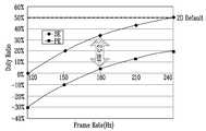
도 5는 동시 발광 방식과 순차 발광 방식의 경우 확보할 수 있는 발광 시간 비율을 비교하는 그래프.
도 6a 및 도 6b는 도 1에 도시된 화소의 실시예에 의한 구성을 나타내는 회로도.
도 7은 도 6a 및 도 6b에 도시된 화소의 구동 타이밍도.
도 8a 및 도 8b는 도 1에 도시된 화소의 다른 실시예에 의한 구성을 나타내는 회로도.
도 9는 도 8a 및 도 8b에 도시된 화소의 구동 타이밍도.1 is a block diagram of an organic light emitting display according to an embodiment of the present invention;
2 is a view showing a driving operation of a simultaneous light emission type according to an embodiment of the present invention;
3 is a view for explaining an example in which a shutter glasses 3D is implemented using an existing sequential light emission method.
4 is a view for explaining an example of implementing a shutter spectacle 3D by a simultaneous light emission method according to an embodiment of the present invention.
FIG. 5 is a graph comparing the emission time ratios that can be secured in the case of the simultaneous light emission method and the sequential light emission method.
6A and 6B are circuit diagrams showing a configuration according to the embodiment of the pixel shown in FIG.
7 is a driving timing diagram of the pixel shown in Figs. 6A and 6B. Fig.
8A and 8B are circuit diagrams showing a configuration according to another embodiment of the pixel shown in FIG.
Fig. 9 is a driving timing diagram of the pixel shown in Figs. 8A and 8B. Fig.
도 1은 본 발명의 실시예에 의한 유기 전계발광 표시장치의 블록도이고, 도 2는 본 발명의 실시예에 의한 동시 발광 방식의 구동 동작을 나타내는 도면이다.FIG. 1 is a block diagram of an organic light emitting display according to an embodiment of the present invention, and FIG. 2 is a diagram illustrating a driving operation of a simultaneous light emission method according to an embodiment of the present invention.
도 1을 참조하면, 본 발명의 실시예에 의한 유기 전계발광 표시장치는 주사선들(S1 내지 Sn), 제어선들(GC1 내지 GCn) 및 데이터선들(D1 내지 Dm)과 접속되는 화소들(140)을 포함하는 화소부(130)와, 주사선들(S1 내지 Sn)을 통해 각 화소에 주사신호를 제공하는 주사 구동부(110)와, 제 1제어선들((GC1 내지 GCn) 및 제 2제어선들(AL1 내지 ALn)을 통해 각 화소에 제 1, 2제어신호를 제공하는 제어선 구동부(160)와, 데이터선들(D1 내지 Dm)을 통해 각 화소에 데이터 신호를 제공하는 데이터 구동부(120)와, 주사 구동부(110), 데이터 구동부(120) 및 제어선 구동부(160)를 제어하기 위한 타이밍 제어부(150)를 구비한다.1, an organic light emitting display according to an exemplary embodiment of the present invention includes
또한, 상기 화소부(130)는 주사선들(S1 내지 Sn) 및 데이터선들(D1 내지 Dm)의 교차부에 위치되는 화소들(140)을 구비한다. 화소들(140)은 외부로부터 제 1전원(ELVDD) 및 제 2전원(ELVSS)을 공급받는다. 이와 같은 화소들(140)은 데이터신호에 대응하여 제 1전원(ELVDD)으로부터 유기발광소자를 경유하여 제 2전원(ELVSS)으로 공급되는 전류량을 제어한다. 그러면, 유기발광소자에서 소정 휘도의 빛이 생성된다.The
단, 본 발명의 실시예의 경우 상기 제 1전원(ELVDD) 및/또는 제 2전원(ELVSS)이 한 프레임의 기간 동안 서로 다른 레벨의 전압값으로 상기 화소부의 각 화소들(140)에 인가됨을 특징으로 한다.However, in the embodiment of the present invention, the first power ELVDD and / or the second power ELVSS are applied to the
이를 위해 상기 제 1전원(ELVDD)의 공급을 제어하는 제 1전원(ELVDD) 구동부(170) 및/또는 상기 제 2전원(ELVSS)의 공급을 제어하는 제 2전원(ELVSS) 구동부(180)이 더 구비되고, 상기 제 1전원(ELVDD) 구동부(170) 및/또는 제 2전원(ELVSS) 구동부(180)는 상기 타이밍 제어부(150)에 의해 제어된다.A first power ELVDD driver 170 for controlling the supply of the first power ELVDD and / or a second
보다 구체적으로 설명하면, 종래의 경우 상기 제 1전원(ELVDD)는 고정된 하이 레벨의 전압으로 제공되고, 제 2전원은 고정된 로우 레벨의 전압으로 화소부의 각 화소에 인가된다.More specifically, in the conventional case, the first power ELVDD is supplied with a fixed high level voltage, and the second power source is applied to each pixel of the pixel portion with a fixed low level voltage.
그러나, 본 발명의 실시예에서는 상기 제 1전원(ELVDD) 및 제 2전원(ELVSS)이 제공됨에 있어 앞서 언급한 바와 같이 한 프레임의 기간 동안 서로 다른 레벨의 전압값으로 인가될 수 있으며, 이는 일 예로 하기된 3가지 방식으로 구현될 수 있다.However, in the embodiment of the present invention, as described above, the first power ELVDD and the second power ELVSS may be applied with different voltage levels during one frame period, For example, it can be implemented in the following three ways.
첫 번째 방식은 상기 제 1전원(ELVDD)이 서로 다른 3가지 레벨의 전압값으로 인가되고, 제 2전원(ELVSS)은 고정된 로우레벨(일 예로 Ground)로 인가된다.In the first method, the first power ELVDD is applied with three different levels of voltage, and the second power ELVSS is applied with a fixed low level (e.g., Ground).
즉, 이 경우 제 2전원(ELVSS) 구동부(180)는 항상 일정한 레벨(GND)의 전압값을 출력하므로 별도의 구동회로로 구현될 필요는 없으며, 이에 대한 회로적 비용은 절감할 수 있으나, 이에 반해 상기 제 1전원(ELVDD)은 3가지 레벨 중 네가티브 전압값(일 예로 ??3V)이 필요하기 때문에 제 1전원(ELVDD) 구동부(170)의 회로 구성이 복잡해 질 수 있다.That is, in this case, since the second
두 번째 방식은 상기 제 1전원(ELVDD) 및 제 2전원(ELVSS)를 모두 각각 2가지 레벨의 전압값으로 각각 인가하도록 구현하는 것으로, 이 경우에는 제 1전원 구동부(170)과 제 2전원 구동부(180)가 모두 구비되어야 한다.In this case, the first power source ELVDD and the second power source ELVSS are respectively applied with voltage values of two levels. In this case, the first power source driver 170 and the second power source driver (180).
세 번째 방식은 상기 첫 번째 방식과 반대로서, 상기 제 1전원(ELVDD)은 고정된 하이 레벨의 전압값으로 인가되고, 제 2전원(ELVSS)은 서로 다른 3가지 레벨의 전압값으로 인가된다.The third method is opposite to the first method in that the first power source ELVDD is applied with a fixed high level voltage value and the second power source ELVSS is applied with three different voltage levels.
즉, 이 경우 제 1전원 구동부(170)은 항상 일정한 레벨의 전압값을 출력하므로 별도의 구동회로로 구현될 필요는 없으며, 이에 대한 회로적 비용은 절감할 수 있으나, 이에 반해 상기 제 2전원(ELVDD)은 3가지 레벨 중 포지티브 전압값이 필요하기 때문에 제 1전원(ELVDD) 구동부(170)의 회로 구성이 복잡해 질 수 있다.
That is, in this case, since the first power source driver 170 always outputs a constant voltage level, it is not necessary to implement a separate driving circuit and the circuit cost can be reduced. On the other hand, the second power source ELVDD requires a positive voltage value among the three levels, the circuit configuration of the first power ELVDD driver 170 may be complicated.
또한, 본 발명의 실시예의 경우 상기 유기 전계발광 표시장치를 구동함에 있어, 순차 발광(Progressive Emission) 방식이 아닌 동시 발광(Simultaneous Emission) 방식으로 구동함을 특징으로 하며, 이는 도 2에 도시된 바와 같이 한 프레임의 기간 중에 데이터가 순차적으로 입력되고, 상기 데이터 입력이 완료된 이후 한 프레임의 데이터가 상기 화소부(130) 전체 즉, 상기 화소부 내의 모든 화소들(140)을 통해 일괄적으로 점등이 수행됨을 말한다.In the embodiment of the present invention, the organic light emitting display device is driven in a simultaneous emission mode instead of a progressive emission mode, Data is sequentially input during one frame period and data of one frame is collectively lighted through all the
즉, 종래의 순차 발광 방식의 경우 각 주사 라인 별로 데이터가 순차적으로 입력되고 곧이어 발광도 순차적으로 수행되는 것이나, 본 발명의 실시예에서는 상기 데이터 입력은 순차적으로 수행되지만, 발광은 데이터 입력이 완료된 후 전체적으로 일괄 수행되는 것이다.That is, in the case of the conventional sequential light emission method, data is sequentially input for each scan line and the light emission is sequentially performed. However, in the embodiment of the present invention, the data input is sequentially performed, It is performed collectively as a whole.
보다 구체적으로 도 2을 참조하면, 본 발명의 실시예에 의한 구동 단계는 크게 (a) 초기화 단계 (b) 리셋 단계 (c) 문턱전압 보상 단계 (d) 주사 단계(데이터 입력 단계) (e) 발광 단계 (f) 발광 오프 단계로 나뉘며, 상기 (d) 주사 단계(데이터 입력 단계)는 각 주사 라인 별로 순차적으로 수행되나, 이를 제외한 나머지 (a) 초기화 단계 (b) 리셋 단계 (c) 문턱전압 보상 단계 (e) 발광 단계 (f) 발광 오프 단계는 도시된 바와 같이 화소부(130) 전체에서 동시에 일괄적으로 수행된다.More particularly, referring to FIG. 2, the driving step according to the embodiment of the present invention includes: (a) an initialization step (b) a reset step (c) a threshold voltage compensation step (d) (A) an initialization step (b) a reset step (c) a step of applying a threshold voltage to the scan line, Compensation Step (e) Light Emission Step (f) The light emission-off step is simultaneously performed all over the
여기서, 상기 (a) 초기화 단계는 각 화소에 구비되는 화소회로의 각 노드 전압을 구동 트랜지스터의 문턱전압 입력때와 동일하게 초기화하는 구간이고, (b) 리셋 단계는 화소부(130)의 각 화소(140)에 인가된 데이터 전압이 리셋되는 단계로서 유기발광소자가 발광되지 않도록 유기발광소자의 애노드 전극의 전압을 캐소드 전극의 전압 이하로 떨어뜨리는 구간이다.(A) initialization step is a period in which each node voltage of a pixel circuit included in each pixel is initialized to be equal to a threshold voltage of a driving transistor, and (b) The voltage of the anode electrode of the organic light emitting diode is lower than the voltage of the cathode electrode so that the organic light emitting diode does not emit light.
또한, 상기 (c) 문턱전압 보상 단계는 상기 각 화소(140)에 구비된 구동 트랜지스터의 문턱전압을 보상하는 구간이며, (f) 발광 오프 단계는 각 화소에서 발광이 수행된 이후 블랙 삽입(black insertion) 또는 디밍(dimming)을 위해 발광을 꺼주는 구간이다.The threshold voltage compensating step (c) is a period for compensating a threshold voltage of the driving transistor included in each
이에 따라 상기 (a) 초기화 단계 (b) 리셋 단계 (c) 문턱전압 보상 단계 (e) 발광 단계 (f) 발광 오프 단계에 인가되는 신호 즉, 각 주사선(S1 내지 Sn)에 인가되는 주사 신호, 각 화소들(140)에 인가되는 제 1전원(ELVDD) 및/또는 제 2전원(ELVSS), 제 1제어선들(GC1 내지 GCn)에 인가되는 제 1제어신호, 제 2제어선들(AL1 내지 ALn)에 인가되는 제 2제어신호는 상기 화소부(130)에 구비된 각 화소들(140)에 대하여 동시에 일괄적으로 각각 정해진 소정의 전압 레벨로 인가된다. 단, 상기 단계 중 초기화 단계는 삭제하여 진행하는 것도 가능하다.(A) an initialization step (b) a reset step (c) a threshold voltage compensation step (e) a light emission step (f) a signal applied to the light-off step, that is, a scan signal applied to each scan line The first power ELVDD and / or the second power ELVSS applied to the
이와 같은 본 발명의 실시예에 의한 "동시 발광 방식"에 의할 경우 각각의 동작 구간((a) 내지 (f) 단계)이 시간적으로 명확히 분리되므로, 각 화소(140)에 구비되는 보상회로의 트랜지스터 및 이를 제어하는 신호선의 수를 줄일 수 있을 뿐 아니라, 셔터(Shutter) 안경식 3D 디스플레이 구현이 용이하다는 장점을 갖게 된다.In the "simultaneous light emission method" according to the embodiment of the present invention, since the respective operation periods (steps (a) to (f)) are clearly separated in terms of time, It is possible to reduce the number of transistors and signal lines for controlling the same, and it is also advantageous that a shutter glasses type 3D display can be easily implemented.
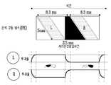
상기 셔터 안경식 3D 디스플레이는 사용자가 좌안/우안의 투과율이 0% 및 100%로 스위치되는 "셔터 안경"을 착용하고 화면을 볼 때, 영상표시장치 즉, 유기 전계발광 표시장치의 화소부에서 디스플레이되는 화면이 각 프레임 별로 좌안 영상과, 우안 영상을 번갈아 출력됨으로써, 사용자는 상기 좌안 영상은 좌안으로만 보이고, 상기 우안 영상은 우안으로만 보이게 되어 입체감이 구현되는 방식을 말한다.The shutter glasses type 3D display is displayed on the image display device, that is, the pixel portion of the organic light emitting display device, when the user wears the "shutter glasses" in which the transmittance of the left / right eye is switched to 0% The screen alternately outputs the left eye image and the right eye image for each frame so that the user views the left eye image only as the left eye and the right eye image as only the right eye, thereby realizing a three-dimensional feeling.
도 3은 기존의 순차 발광 방식으로 셔텨 안경식 3D를 구현한 예를 설명하는 도면이고, 도 4는 본 발명의 실시예에 의한 동시 발광 방식으로 셔터 안경식 3D를 구현한 예를 설명하는 도면이다.FIG. 3 is a view for explaining an example of implementing a shutter glasses type 3D according to a conventional sequential light emission method, and FIG. 4 is a view for explaining an example of implementing a shutter glasses type 3D by a simultaneous light emission method according to an embodiment of the present invention.
또한, 도 5는 동시 발광 방식과 순차 발광 방식의 경우 확보할 수 있는 발광 시간 비율을 비교하는 그래프이다.5 is a graph for comparing the emission time ratio that can be secured for the simultaneous light emission method and the sequential light emission method.
이와 같은 셔터 안경식 3D 디스플레이를 구현함에 있어 앞서 언급한 종래의 순차 발광 방식으로 화면을 출력하는 경우에는 도 3에 도시된 바와 같이 상기 셔터 안경의 응답 시간(일 예로 2.5ms)이 유한 하기 때문에 상기 좌안/우안 영상간의 크로스토크(cross talk) 현상을 방지하기 위해 상기 응답 시간만큼 발광을 꺼주어야 한다.In the case of realizing such a shutter glasses type 3D display, in the case of outputting a screen by the above-mentioned conventional sequential light emission method, since the response time (for example, 2.5 ms) of the shutter glasses is finite as shown in FIG. 3, It is necessary to turn off the light emission for the response time in order to prevent the cross talk phenomenon between the right eye image and the right eye image.
즉, 좌안 영상이 출력되는 프레임(n번째 프레임)과 이에 이어서 우안 영상이 출력되는 프레임(n+1번째 프레임) 사이에 상기 응답 시간만큼 비발광 구간을 추가로 생성해야 하므로 발광 시간 확보 즉, 발광 시간 비율(Duty ratio)이 낮아진다는 단점이 있다.That is, since a non-emission period is additionally generated by the response time between the frame (n-th frame) from which the left eye image is outputted and the frame (n + 1) -th frame from which the right eye image is output, The duty ratio is lowered.
이에 본 발명의 실시예에 의한 "동시 발광 방식"의 경우 도 4를 참조하면, 앞서 설명한 바와 같이 발광 단계가 화소부 전체에서 동시에 일괄적으로 수행되고, 상기 발광 단계 이외의 구간에서는 비 발광이 수행됨에 따라, 좌안 영상이 출력되는 구간과 우안 영상이 출력되는 구간 사이의 비 발광 구간이 자연스럽게 확보된다.Referring to FIG. 4, in the case of the "simultaneous light emission type" according to the embodiment of the present invention, the light emission step is performed simultaneously all over the pixel part as described above, and the non-light emission is performed in a section other than the light emission step , A non-emission period between the section in which the left eye image is output and the section in which the right eye image is output is naturally ensured.
즉, n번째 프레임의 발광구간과 n+1번째 프레임의 발광구간 사이의 구간으로서 발광오프 구간, 리셋 구간, 문턱전압 보상 구간이 비 발광되는 구간이므로 상기 구간의 전체 시간을 상기 셔텨 안경의 응답 시간(일 예로 2.5ms)과 동기시키면 종래의 순차 발광 방식과 달리 별도로 발광 시간 비율(Duty ratio)을 줄이지 않아도 된다.That is, since the light emission off period, the reset period, and the threshold voltage compensating period are non-light emitting periods as a period between the light emitting period of the nth frame and the light emitting period of the (n + 1) th frame, (For example, 2.5 ms), it is not necessary to reduce the duty ratio separately from the conventional sequential light emitting method.
따라서, 셔터 안경식 3D 디스플레이를 구현함에 있어 상기 "동시 발광 방식"이 종래의 "순차 발광 방식"에 비해 상기 셔터 안경의 응답 시간만큼의 발광시간 비율(duty ratio)을 확보할 수 있으므로 보다 향상된 성능 구현이 가능하게 된다. 이는 도 5의 그래프를 통해 확인할 수 있다.
Therefore, in realizing the shutter glasses type 3D display, the "simultaneous light emission method" can secure the duty ratio of the light emission time as long as the response time of the shutter glasses as compared with the conventional "sequential light emission method"Lt; / RTI > This can be confirmed by the graph of FIG.
도 6a 및 도 6b는 도 1에 도시된 화소의 실시예에 의한 구성을 나타내는 회로도이고, 도 7은 도 6a 및 도 6b에 도시된 화소의 구동 타이밍도이다.FIGS. 6A and 6B are circuit diagrams showing the configuration of the pixel shown in FIG. 1, and FIG. 7 is a driving timing diagram of the pixels shown in FIGS. 6A and 6B.
먼저 도 6a를 참조하면, 본 발명의 실시예에 의한 화소(140)는 유기발광 소자(Organic Light Emitting Diode, OLED)와, 유기발광소자(OLED)로 전류를 공급하기 위한 화소회로(142)를 구비한다.6A, a
유기발광소자(OLED)의 애노드전극은 화소회로(142)에 접속되고, 캐소드전극은 제 2전원(ELVSS)에 접속된다. 이와 같은 유기발광소자(OLED)는 화소회로(142)로부터 공급되는 전류에 대응하여 소정 휘도의 빛을 생성한다.The anode electrode of the organic light emitting element OLED is connected to the
단, 본 발명의 실시예의 경우 화소부(130)를 구성하는 각 화소(140)는, 한 프레임의 일부 기간(앞에 언급한 (d) 단계)에 대하여 주사선(S1 내지 Sn)에 순차적으로 주사신호가 공급될 때, 데이터선(D1 내지 Dm)으로 공급되는 데이터신호를 공급받으나, 한 프레임의 나머지 기간((a), (b), (c), (e), (f) 단계)에 대해서는 각 주사선(S1 내지 Sn)에 인가되는 주사 신호, 각 화소들(140)에 인가되는 제 1전원(ELVDD) 및/또는 제 2전원(ELVSS), 제 1제어선(GC1 내지 GCn), 제 2제어선(AL1 내지 ALn)에 각각 인가되는 제 1, 2제어신호들이 동시에 일괄적으로 각각 정해진 소정의 전압 레벨로 상기 각 화소(140)에 인가된다.However, in the embodiment of the present invention, each of the
이에 상기 각 화소(140)에 구비되는 화소회로(142)는 4개의 트랜지스터(P1 내지 P4) 및 2개의 커패시터(C1, C2)를 구비한다.The
여기서, 제 1트랜지스터(P1)의 게이트 전극은 주사선(S)에 접속되고, 제 1전극은 데이터선(D)에 접속된다. 그리고, 제 1트랜지스터(P1)의 제 2전극은 제 1노드(N1)에 접속된다.Here, the gate electrode of the first transistor P1 is connected to the scanning line S, and the first electrode is connected to the data line D. The second electrode of the first transistor P1 is connected to the first node N1.
즉, 상기 제 1트랜지스터(P1)의 게이트 전극에는 주사신호(Scan(n))가 입력되고, 제 1전극으로는 데이터신호(Data(t))가 입력된다.That is, the scan signal Scan (n) is input to the gate electrode of the first transistor P1, and the data signal Data (t) is input to the first electrode P1.
또한, 제 2트랜지스터(P2)의 게이트 전극은 제 2노드(N2)에 접속되고, 제 1전극은 제 1전원(ELVDD(t))에 접속되며, 제 2전극은 유기발광소자의 애노드 전극에 접속된다. 여기서, 상기 제 2트랜지스터(P2)는 구동 트랜지스터로서의 역할을 수행한다.The gate electrode of the second transistor P2 is connected to the second node N2 and the first electrode is connected to the first power source ELVDD (t) and the second electrode is connected to the anode electrode of the organic light- Respectively. Here, the second transistor P2 serves as a driving transistor.
또한, 상기 제 1노드(N1) 및 제 2트랜지스터(P2)의 제 1전극 즉, 제 1전원(ELVDD(t)) 사이에 제 1커패시터(C1)이 접속되고, 상기 제 1노드(N1) 및 제 2노드(N2) 사이에는 제 2커패시터(C2)가 접속된다.A first capacitor C1 is connected between a first electrode of the first node N1 and the first power source ELVDD (t) of the second transistor P2, And a second capacitor C2 is connected between the first node N2 and the second node N2.
또한, 제 3트랜지스터(P3)의 게이트 전극은 제 1제어선(GC)에 접속되고, 제 1전극은 상기 제 2트랜지스터(P2)의 게이트 전극과 접속되며, 제 2전극은 상기 유기발광소자의 애노드 전극 즉, 제 2트랜지스터(P2)의 제 2전극과 접속된다.The gate electrode of the third transistor P3 is connected to the first control line GC. The first electrode of the third transistor P3 is connected to the gate electrode of the second transistor P2. The second electrode of the organic light- And is connected to the anode electrode, that is, the second electrode of the second transistor P2.
이에 따라 상기 제 3트랜지스터(P3)의 게이트 전극으로는 제어신호(GC(t))가 입력되며, 상기 제 3트랜지스터가 턴 온되는 경우 상기 제 2트랜지스터(P2)는 다이오드 연결된다.Accordingly, the control signal GC (t) is input to the gate electrode of the third transistor P3, and when the third transistor is turned on, the second transistor P2 is diode-connected.
또한, 상기 유기발광소자의 캐소드 전극은 제 2전원(ELVSS(t))와 연결된다.Also, the cathode electrode of the organic light emitting diode is connected to the second power source ELVSS (t).
또한, 제 4트랜지스터(P4)의 게이트 전극은 제 2제어선(AL)에 접속되고, 제 1전극은 데이터선(D)과 접속되며, 제 2전극은 상기 제 1트랜지스터(P1)의 제 2전극 즉, 제 1노드(N1)에 접속된다.The gate electrode of the fourth transistor P4 is connected to the second control line AL and the first electrode thereof is connected to the data line D and the second electrode of the fourth transistor P4 is connected to the second That is, the first node N1.
이 때, 도 6a 및 도 6b에 도시된 실시예는 제 4트랜지스터의 제 1전극(소스 전극)에 인가되는 신호가 상이할 뿐 그 외의 구성요소는 동일하다.In this case, the embodiment shown in Figs. 6A and 6B differs in signal applied to the first electrode (source electrode) of the fourth transistor, but the other components are the same.
즉, 도 6b에 도시된 실시예의 경우 상기 제 4트랜지스터(P4')의 제 1전극이 상기 데이터선(D)이 아닌 제 3전원(Vsus)에 연결되는 점에서 그 차이가 있다. 따라서, 상기 제 4트랜지스터(P4')의 게이트 전극은 제 2제어선(AL)에 접속되고, 제 1전극은 제 3전원(Vsus)과 접속되며, 제 2전극은 상기 제 1트랜지스터(P1)의 제 2전극 즉, 제 1노드(N1)에 접속된다. 여기서, 상기 제 3전원(Vsus)는 정전압원으로서 하이 레벨의 전압을 제공한다.That is, in the embodiment shown in FIG. 6B, the first electrode of the fourth transistor P4 'is connected to the third power source Vsus other than the data line D, which is different from the first power source V4. Therefore, the gate electrode of the fourth transistor P4 'is connected to the second control line AL, the first electrode thereof is connected to the third power source Vsus, the second electrode is connected to the first transistor P1, That is, the first node N1. Here, the third power supply (Vsus) provides a high level voltage as a constant voltage source.
이 때, 상기 도 6b의 실시예의 경우 데이터선(D)에서 인가되는 전압 대신 정전압 원인 제 3전원(Vsus)을 이용함으로써, 데이터 구동부의 전류 부담을 줄일 수 있다는 장점이 있다.6B, there is an advantage that the current load of the data driver can be reduced by using the third power source (Vsus) which is a constant voltage instead of the voltage applied to the data line (D).
단, 상기 제 2제어선(AL)에 인가되는 제 2제어신호에 의해 제 4트랜지스터가 턴 온되면, 도 6a, 도 6b의 실시예 모두 동일한 레벨 즉, 하이 레벨의 전압이 제 1전극으로 인가되므로 도 6a, 도 6b에 도시된 실시예에 의한 회로는 그 동작이 서로 동일하게 된다.However, when the fourth transistor is turned on by the second control signal applied to the second control line AL, the same level, that is, a high level voltage is applied to the first electrode in all of the embodiments of FIGS. 6A and 6B The operation of the circuit according to the embodiment shown in Figs. 6A and 6B becomes equal to each other.
도 6a, 도 6b에 도시된 실시예의 경우 상기 제 1 내지 제 4트랜지스터(P1 내지 P4)는 모두 PMOS로 구현된다.In the embodiment shown in FIGS. 6A and 6B, the first to fourth transistors P1 to P4 are all implemented as PMOS.
앞서 설명한 바와 같이 본 발명의 실시예에 의한 상기 각 화소(140)는 "동시 발광 방식"으로 구동됨을 특징으로 하며, 이는 구체적으로 도 7에 도시된 바와 같이 각 프레임 별로 초기화 구간(Int), 리셋 구간(Reset), 문턱전압 보상 구간(Vth), 주사/ 데이터 입력 구간(Scan), 발광 구간(Emission) 및 발광 오프 구간(Off)으로 구분된다.As described above, each of the
이 때, 상기 주사/ 데이터 입력 구간에 대해서는 주사신호가 각 주사선에 대해 순차적으로 입력되고, 이에 대응하여 각 화소에 데이터 신호가 순차적으로 입력되나, 이외의 구간에 대해서는 기 설정된 레벨의 전압값을 갖는 신호 즉, 제 1전원(ELVDD(t)) 및/또는 제 2전원(ELVSS(t)), 주사신호(Scan(n)), 제 1제어신호(GC(t)), 제 2제어신호(AL(t)), 데이터신호(Data(t))가 화소부를 구성하는 전체 각 화소(140)에 일괄적으로 인가된다. At this time, a scan signal is sequentially input to each scan line for the scan / data input period, and data signals are sequentially input to each pixel corresponding to the scan signal / data input period, but a voltage value of a predetermined level A first control signal GC (t), a second control signal (second control signal), and a second control signal AL (t) and the data signal Data (t) are collectively applied to all the
즉, 각 화소(140)에 구비된 구동 트랜지스터의 문턱전압 보상 및 각 화소의 발광 동작은 프레임 별로 화소부 내의 모든 화소(140)에서 동시에 구현됨을 특징으로 한다.That is, the threshold voltage compensation of the driving transistor included in each
단, 본 발명의 실시예의 경우 상기 제 1전원(ELVDD(t)) 및/또는 제 2전원(ELVSS(t))이 제공됨에 있어서 앞서 언급한 바와 같이 3가지 방식으로 구현될 수 있으나, 설명의 편의를 위해 도 7에서는 상기 제 1전원(ELVDD) 및 제 2전원(ELVSS)이 각각 2가지 레벨의 전압값으로 인가되는 것으로 설명한다.However, in the embodiment of the present invention, as described above, the first power ELVDD (t) and / or the second power ELVSS (t) may be implemented in three ways, In FIG. 7, the first power ELVDD and the second power ELVSS are respectively applied with voltage values of two levels for convenience.
도 6 및 도 7을 참조하여 본 발명의 실시예에 의한 화소의 구동방법 즉, 앞서 설명한 각 구간(초기화 구간(Int), 리셋 구간(Reset), 문턱전압 보상 구간(Vth), 주사/ 데이터 입력 구간(Scan), 발광 구간(Emission) 및 발광 오프 구간(Off))에서의 동작을 순차적으로 설명하면 다음과 같다.6 and 7, a method of driving a pixel according to an exemplary embodiment of the present invention will be described with reference to FIGS. 6 and 7, The operation in the scan period, the emission period, and the light emission period Off will be sequentially described below.
먼저 초기화 구간에서는 제 1전원(ELVDD(t)), 제 2전원(ELVSS(t)), 주사신호(Scan(n)) 및 제 1제어신호(GC(t))가 모두 하이 레벨로 인가되고, 제 2제어신호(AL(t)) 만이 로우 레벨로 인가된다.In the initialization period, the first power ELVDD (t), the second power ELVSS (t), the scan signal Scan (n), and the first control signal GC (t) , Only the second control signal AL (t) is applied at a low level.
즉, 도 6a, 6b에 도시된 화소회로에 의할 경우 제 4트랜지스터(P4 또는 P4')만 턴 온되고, 나머지 트랜지스터는 모두 턴 오프 상태에 있으며, 상기 제 4트랜지스터가 턴 온됨에 의해 상기 제 1노드(N1)로는 초기화 전압으로서 하이 레벨의 전압이 인가된다.6A and 6B, only the fourth transistor P4 or P4 'is turned on and all the remaining transistors are in the turned-off state, and the fourth transistor is turned on, And a high level voltage is applied to the one node N1 as an initialization voltage.
이 때, 도 6a의 실시예에서는 상기 초기화 전압이 데이터선을 통해 전달되고, 도 6b의 실시예의 경우에는 제 3전원(Vsus)선을 통해 인가된다.In this case, the initialization voltage is transmitted through the data line in the embodiment of FIG. 6A, and is applied through the third power source (Vsus) line in the embodiment of FIG. 6B.
또한, 상기 초기화 단계는 화소부를 구성하는 각 화소에 일괄적으로 적용되는 것이므로, 초기화 단계에서 인가되는 신호들 즉, 제 1전원(ELVDD(t)), 주사신호(Scan(n)), 제 1제어신호(GC(t)), 제 2제어신호(AL(t)) 및 데이터 신호(Data(t))는 각각 설정된 레벨의 전압값으로 상기 모든 화소에 동시에 인가된다.Since the initialization step is applied collectively to each pixel constituting the pixel portion, the signals applied in the initialization step, i.e., the first power source ELVDD (t), the scan signal Scan (n) The control signal GC (t), the second control signal AL (t) and the data signal Data (t) are simultaneously applied to all of the pixels at the set voltage level.
단, 상기 초기화 구간은 삭제 가능한 구간으로서, 상기 초기화 구간에 대해서는 모든 트랜지스터를 턴 오프 시킨 뒤 이후 리셋 단계부터 진행하는 것도 가능하다. 즉, 상기 초기화 구간에서 제 2제어신호(AL(t))가 하이 레벨로 인가될 수도 있다.However, it is also possible that the initialization period is an erasable period, and all the transistors are turned off for the initialization period, and then the reset period is started. That is, the second control signal AL (t) may be applied at a high level in the initialization period.
다음으로 상기 리셋 구간은 화소부(130)의 각 화소(140) 즉, 도 6에 도시된 화소에 인가된 데이터 전압이 리셋되는 구간으로서 유기발광소자가 발광되지 않도록 유기발광소자의 애노드 전극의 전압을 캐소드 전극의 전압 이하로 떨어뜨리는 단계이다.Next, the reset period is a period during which the data voltage applied to each
상기 리셋 구간에서는 도 7에 도시된 바와 같이 제 1전원(ELVDD(t))이 로우 레벨로 인가되고, 나머지 제 2전원(ELVSS(t)), 주사신호(Scan(n)) 및 제 1제어신호(GC(t)), 제 2제어신호(AL(t))가 모두 하이 레벨로 인가된다.7, the first power ELVDD (t) is applied at a low level and the remaining second power ELVSS (t), the scan signal Scan (n) The signal GC (t) and the second control signal AL (t) are both applied at a high level.
이와 같이 상기 제 1전원(ELVDD(t))이 로우 레벨로 인가되면, 상기 제 1커패시터(C1) 및 제 2커패시터(C2)의 커플링 효과에 의해 상기 제 1노드(N1)의 전압 또한 초기화 구간에서의 전압값보다 낮아지게 된다.When the first power ELVDD (t) is applied at a low level, the voltage of the first node N1 is also initialized by the coupling effect of the first capacitor C1 and the second capacitor C2 Is lower than the voltage value in the section.
이에 PMOS로 구현된 상기 제 2트랜지스터(P2)가 턴 온되고, 제 2트랜지스터(P2)의 제 1, 2전극 간 전류 통로가 형성됨에 따라 상기 제 2트랜지스터(P2)의 제 2전극에 접속된 유기발광소자의 애노드 전극에 충전된 전압은 상기 제 1전원의 전압값으로 떨어지게 된다. 즉, 유기발광소자의 애노드 전극 전압이 리셋되는 것이다.The second transistor P2 implemented by the PMOS is turned on and the current path between the first and second electrodes of the second transistor P2 is formed so that the second transistor P2 is connected to the second electrode of the second transistor P2 The voltage charged in the anode electrode of the organic light emitting diode drops to the voltage value of the first power source. That is, the anode electrode voltage of the organic light emitting diode is reset.
또한, 상기 리셋 단계는 화소부를 구성하는 각 화소에 일괄적으로 적용되는 것이므로, 초기화 단계에서 인가되는 신호들 즉, 제 1전원(ELVDD(t)), 주사신호(Scan(n)), 제 1제어신호(GC(t)), 제 2제어신호(AL(t)) 및 데이터 신호(Data(t))는 각각 설정된 레벨의 전압값으로 상기 모든 화소에 동시에 인가된다.In addition, since the reset step is applied collectively to each pixel constituting the pixel portion, signals applied in the initialization step, i.e., the first power ELVDD (t), the scan signal Scan (n) The control signal GC (t), the second control signal AL (t) and the data signal Data (t) are simultaneously applied to all of the pixels at the set voltage level.
다음으로 문턱전압 보상 구간은 화소부(130)의 각 화소(140)에 구비된 구동 트랜지스터(P2)의 문턱전압이 커패시터(Cst)에 저장되는 구간으로서 이는 이후 각 화소에 데이터 전압이 충전될 때 구동 트랜지스터의 문턱전압 편차에 의한 불량을 제거하는 역할을 한다.The threshold voltage compensation period is a period in which the threshold voltage of the driving transistor P2 provided in each
상기 문턱전압 보상 구간에서는 도 7에 도시된 바와 같이 제 1전원(ELVDD(t)), 제 2전원(ELVSS(t)), 주사신호(Scan(n))가 하이 레벨로 인가되고, 제 1제어신호(GC(t)) 및 제 2제어신호(AL(t))는 로우 레벨로 인가된다.7, the first power ELVDD (t), the second power ELVSS (t), and the scan signal Scan (n) are applied at a high level, and the first The control signal GC (t) and the second control signal AL (t) are applied at a low level.
이 때, 상기 제 1제어신호(GC(t))가 로우 레벨로 인가됨에 의해 상기 제 3트랜지스터(P3)가 턴 온되고, 이에 제 2트랜지스터(P2)의 게이트 전극 및 제 3트랜지스터(P3)의 제 2전극이 전기적으로 연결되어 결과적으로 상기 제 2트랜지스터(P2)는 다이오드로서 동작하게 된다.At this time, the third transistor P3 is turned on by the first control signal GC (t) being applied at a low level, and the gate electrode of the second transistor P2 and the third transistor P3 are turned on, The second electrode of the second transistor P2 is electrically connected, resulting in that the second transistor P2 operates as a diode.
따라서, 상기 제 2노드(N2)와 연결된 제 2캐패시터(C2)에는 상기 제 2트랜지스터(P2)의 문턱전압이 저장되며, 이는 이후 상기 데이터 입력 구간에서 발생되는 구동 트랜지스터(제 2트랜지스터(P2))의 문턱전압과 상쇄되어 최종적으로 유기발광소자에 인가되는 전류에서는 상기 구동 트랜지스터의 문턱전압 편차에 의한 불량이 제거되는 것이다.Therefore, the threshold voltage of the second transistor P2 is stored in the second capacitor C2 connected to the second node N2, and the threshold voltage of the second transistor P2, which is generated in the data input period, , The defect caused by the threshold voltage deviation of the driving transistor is eliminated at the current finally applied to the organic light emitting element.
또한, 문턱전압 보상 단계 역시 화소부를 구성하는 각 화소에 일괄적으로 적용되는 것이므로, 문턱전압 보상 단계에서 인가되는 신호들 즉, 제 1전원(ELVDD(t)), 주사신호(Scan(n)), 제어신호(GC(t)) 및 데이터 신호(Data(t))는 각각 설정된 레벨의 전압값으로 상기 모든 화소에 동시에 인가된다.In addition, since the threshold voltage compensating step is also applied to each pixel constituting the pixel portion, the signals applied in the threshold voltage compensating step, that is, the first power source ELVDD (t), the scanning signal Scan (n) , The control signal GC (t) and the data signal Data (t) are simultaneously applied to all of the pixels at the set voltage level.
본 발명의 실시예의 경우 상기 초기화 구간, 리셋 구간, 문턱전압 보상 구간에 대하여 주사신호가 그대로 하이 레벨을 유지하여 출력하는 동작을 수행하는 바, 기존의 "순차 구동 방식"에 적용되는 일반적인 게이트 구동부를 활용하여도 전혀 문제가 없다.In the exemplary embodiment of the present invention, the scan signal is maintained at a high level for the initialization period, the reset period, and the threshold voltage compensation period, There is no problem at all.
즉, 본 발명의 실시예는 "동시 발광 방식"을 구현하기 위해 게이트 구동부에서 각 주사선으로 출력되는 신호가 상기 제 1노드(N1)의 전압을 초기화 하기 위해 동시에 로우 레벨로 인가되어야 하는 단점을 상기 제 4트랜지스터 및 이를 제어하는 제 2제어신호(AL(t))가 인가됨을 통해 극복 할 수 있으며, 이는 상기 "동시 발광 방식"으로 구동하는 경우에도 범용 게이트 구동 IC 도입이 가능하고, 게이트 구동부를 패널에 실장함에 있어서도 회로 차지 면적을 최소화할 수 있게 된다.That is, in order to realize the "simultaneous light emission method", the embodiment of the present invention has the disadvantage that the signal output from the gate driver to each scanning line must be simultaneously applied at a low level in order to initialize the voltage of the first node N1 And the second control signal AL (t) for controlling the fourth transistor may be applied to the gate driver. In this case, even when driving by the "simultaneous light emission method" The circuit charge area can be minimized even when mounted on a panel.
상기 문턱 전압 보상 구간 이후, 주사/ 데이터 입력 구간에 대해서는 로우 레벨의 주사신호가 각 주사선에 대해 순차적으로 입력되고, 이에 대응하여 각 주사선별로 연결된 화소에 데이터 신호가 순차적으로 입력된다.After the threshold voltage compensation period, a low level scan signal is sequentially input to each scan line in the scan / data input period, and data signals are sequentially input to the pixels connected to each scan line corresponding thereto.
상기 구간 동안에는 도 7에 도시된 바와 같이 제 1제어신호(GC(t)) 및 제 2제어신호(AL(t))는 하이 레벨로 인가되며, 이에 제 4트랜지스터(P4, P4') 및 제 3트랜지스터(P3)는 턴 오프된다.7, the first control signal GC (t) and the second control signal AL (t) are applied at a high level, and the fourth transistor P4, P4 ' 3 transistor P3 is turned off.
즉, 상기 구간은 기존의 "순차 구동 방식"과 동일한 방식으로 주사신호 및 데이터 신호가 인가된다.That is, the scanning signal and the data signal are applied to the section in the same manner as the conventional "sequential driving method ".
단, 상기 구간에서는 상기 제 2전원(ELVSS(t))이 제 1전원(ELVDD(t))와 동일한 하이 레벨로 인가되고 있으므로 유기발광소자와 제 1전원(ELVDD(t))간에 전류 경로가 형성되지 않아 실질적으로는 유기발광소자로는 전류가 흐르지 않는다. 즉, 발광이 수행되지 않는다.Since the second power source ELVSS (t) is applied at the same high level as the first power source ELVDD (t) in the above section, a current path between the organic light emitting diode and the first power source ELVDD (t) So that no electric current flows to the organic light emitting element. That is, no light emission is performed.
다음으로 발광 구간은 화소부(130)의 각 화소(140)에 저장된 데이터 전압에 대응되는 전류가 각 화소에 구비된 유기발광소자로 제공되어 발광이 수행되는 구간으로서, 상기 발광 구간에서는 앞선 주사/ 데이터 입력 구간과 달리 제 2전원(ELVSS(t))이 로우 레벨로 인가된다.Next, the light emitting period is a period in which a current corresponding to the data voltage stored in each
이에 따라, 상기 구간에서는 상기 제 2전원(ELVSS(t))가 로우 레벨로 인가되고 있으므로 제 2트랜지스터(P2)의 턴온에 의해 상기 제 1전원과 유기발광소자의 캐소드 전극까지의 전류 경로가 형성되며, 이에 따라 상기 제 2트랜지스터(P2)의 Vgs 전압값 즉, 제 2트랜지스터의 게이트 전극과 제 1전극의 전압차에 해당하는 전압에 대응되는 전류가 상기 유기발광소자에 인가되며, 이에 대응되는 밝기로 발광하는 것이다.Accordingly, since the second power source ELVSS (t) is applied at a low level in the above-described period, the current path from the first power source to the cathode electrode of the organic light emitting element is formed by turning on the second transistor P2 A current corresponding to a voltage corresponding to a voltage difference between the gate electrode of the second transistor and the first electrode is applied to the organic light emitting element, It emits light with brightness.
단, 상기 발광 단계 역시 화소부를 구성하는 각 화소에 일괄적으로 적용되는 것이므로, 발광 단계에서 인가되는 신호들 즉, 제 1전원(ELVDD(t)), 주사신호(Scan(n)), 제 1제어신호(GC(t)), 제 2제어신호(AL(t)) 및 데이터 신호(Data(t))는 각각 설정된 레벨의 전압값으로 상기 모든 화소에 동시에 인가된다.Since the light emitting step is also applied collectively to each pixel constituting the pixel portion, signals applied in the light emitting step, i.e., the first power ELVDD (t), the scan signal Scan (n) The control signal GC (t), the second control signal AL (t) and the data signal Data (t) are simultaneously applied to all of the pixels at the set voltage level.
다음으로 이와 같이 화소부 전체의 발광이 수행된 이후에는 상기 제 2전원(ELVSS(t))가 하이 레벨로 제공되어 발광 오프 단계를 수행한다.Next, after the light emission of the entire pixel portion is performed, the second power ELVSS (t) is supplied to the high level to perform the light-off step.
이는 발광 동작 이후 블랙 삽입(black insertion) 또는 디밍(dimming)을 위해 발광을 꺼주는 기간으로서, 유기발광소자의 애노드 전극의 전압값은 이전에 유기발광소자가 발광하고 있었으면 수십 us 이내로 발광이 오프되는 전압까지 떨어지게 된다.
This is a period during which the light emission is turned off for black insertion or dimming after the light emitting operation, and the voltage value of the anode electrode of the organic light emitting element is turned off within several tens of seconds if the organic light emitting element had previously emitted light Voltage.
도 8a 및 도 8b는 도 1에 도시된 화소의 다른 실시예에 의한 구성을 나타내는 회로도이고, 도 9는 도 8a 및 도 8b에 도시된 화소의 구동 타이밍도이다.8A and 8B are circuit diagrams showing a configuration according to another embodiment of the pixel shown in FIG. 1, and FIG. 9 is a driving timing diagram of the pixels shown in FIGS. 8A and 8B.
먼저 도 8a을 참조하면, 본 발명의 다른 실시예에 의한 화소(240)는 유기발광 소자(Organic Light Emitting Diode, OLED)와, 유기발광소자(OLED)로 전류를 공급하기 위한 화소회로(242)를 구비한다.8A, a
유기발광소자(OLED)의 애노드전극은 화소회로(242)에 접속되고, 캐소드전극은 제 2전원(ELVSS)에 접속된다. 이와 같은 유기발광소자(OLED)는 화소회로(242)로부터 공급되는 전류에 대응하여 소정 휘도의 빛을 생성한다.The anode electrode of the organic light emitting device OLED is connected to the
단, 본 발명의 실시예의 경우 화소부(130)를 구성하는 각 화소(140)는, 한 프레임의 일부 기간에 대하여 주사선(S1 내지 Sn)에 순차적으로 주사신호가 공급될 때, 데이터선(D1 내지 Dm)으로 공급되는 데이터신호를 공급받으나, 한 프레임의 나머지 기간에 대해서는 각 주사선(S1 내지 Sn)에 인가되는 주사 신호, 각 화소들(140)에 인가되는 제 1전원(ELVDD), 제 1제어선(GC1 내지 GCn), 제 2제어선(AL1 내지 ALn)에 각각 인가되는 제 1, 2제어 신호들이 동시에 일괄적으로 각각 정해진 소정의 전압 레벨로 상기 각 화소(140)에 인가된다.However, in the embodiment of the present invention, each
이에 상기 각 화소(140)에 구비되는 화소회로(142)는 4개의 트랜지스터(M1 내지 M3) 및 1개의 커패시터(Cst)를 구비한다.The
여기서, 제 1트랜지스터(M1)의 게이트 전극은 주사선(S)에 접속되고, 제 1전극은 데이터선(D)에 접속된다. 그리고, 제 1트랜지스터(M1)의 제 2전극은 제 1노드(N1)에 접속된다.Here, the gate electrode of the first transistor M1 is connected to the scanning line S, and the first electrode is connected to the data line D. The second electrode of the first transistor M1 is connected to the first node N1.
즉, 상기 제 1트랜지스터(M1)의 게이트 전극에는 주사신호(Scan(n))가 입력되고, 제 1전극으로는 데이터신호(Data(t))가 입력된다.That is, the scan signal Scan (n) is input to the gate electrode of the first transistor M1, and the data signal Data (t) is input to the first electrode of the first transistor M1.
제 2트랜지스터(M2)의 게이트 전극은 제 1노드(N1)에 접속되고, 제 1전극은 유기발광소자의 애노드 전극에 접속된다. 그리고, 제 2트랜지스터(M2)의 제 2전극은 제 3트랜지스터(M3)의 제 1, 2전극을 통해 제 1전원(ELVDD(t))과 연결된다. 상기 제 2트랜지스터(M2)는 구동 트랜지스터로서의 역할을 수행한다.The gate electrode of the second transistor M2 is connected to the first node N1, and the first electrode is connected to the anode electrode of the organic light emitting element. The second electrode of the second transistor M2 is connected to the first power ELVDD (t) through the first and second electrodes of the third transistor M3. The second transistor M2 serves as a driving transistor.
즉, 상기 제 3트랜지스터(M3)의 게이트 전극은 제 1제어선(GC)에 접속되고, 제 1전극은 상기 제 2트랜지스터(M2)의 제 2전극과 접속되며, 제 2전극은 상기 제 1전원(ELVDD(t))와 접속된다.That is, the gate electrode of the third transistor M3 is connected to the first control line GC, the first electrode of the third transistor M3 is connected to the second electrode of the second transistor M2, And is connected to the power source ELVDD (t).
이에 따라 상기 제 3트랜지스터(M3)의 게이트 전극으로는 제어신호(GC(t))가 입력되고, 제 2전극으로는 소정의 레벨로 가변되어 제공되는 제 1전원(ELVDD(t))가 입력된다.The first power ELVDD (t) supplied to the gate electrode of the third transistor M3 is supplied with a control signal GC (t) and the second electrode thereof is varied to a predetermined level. do.
또한, 상기 유기발광소자의 캐소드 전극은 제 2전원(ELVSS)와 연결되며, 상기 제 2트랜지스터(M2)의 게이트 전극 즉, 제 1노드(N1)와 제 2트랜지스터(M2)의 제 1전극 즉, 유기발광소자의 애노드 전극 사이에는 커패시터(Cst)가 접속된다.The cathode electrode of the organic light emitting diode is connected to a second power source ELVSS and a gate electrode of the second transistor M2 is connected to a first electrode N1 of the second transistor M2, , And a capacitor (Cst) is connected between the anode electrode of the organic light emitting diode.
또한, 상기 제 4트랜지스터(M4)의 게이트 전극은 제 2제어선(AL)에 접속되고, 제 1전극은 상기 데이터선(D)에 접속되며, 제 2전극은 상기 제 1트랜지스터(M1)의 제 2전극 즉, 제 1노드(N1)에 접속된다.The gate electrode of the fourth transistor M4 is connected to the second control line AL. The first electrode of the fourth transistor M4 is connected to the data line D, That is, the first node N1.
이 때, 도 8a 및 도 8b에 도시된 실시예는 제 4트랜지스터의 제 1전극(소스 전극)에 인가되는 신호가 상이할 뿐 그 외의 구성요소는 동일하다.In this case, the embodiment shown in Figs. 8A and 8B differs in signal applied to the first electrode (source electrode) of the fourth transistor, but the other components are the same.
즉, 도 8b에 도시된 실시예의 경우 상기 제 4트랜지스터(M4')의 제 1전극이 상기 데이터선(D)이 아닌 제 4전원(Vsus')에 연결되는 점에서 그 차이가 있다. 따라서, 상기 제 4트랜지스터(M4')의 게이트 전극은 제 2제어선(AL)에 접속되고, 제 1전극은 제 4전원(Vsus')과 접속되며, 제 2전극은 상기 제 1트랜지스터(M1)의 제 2전극 즉, 제 1노드(N1)에 접속된다. 여기서, 상기 제 4전원(Vsus')는 정전압원으로서 로우 레벨의 전압을 제공한다.That is, in the embodiment shown in FIG. 8B, the first electrode of the fourth transistor M4 'is connected to the fourth power source Vsus' other than the data line D. Therefore, the gate electrode of the fourth transistor M4 'is connected to the second control line AL, the first electrode thereof is connected to the fourth power source Vsus', and the second electrode thereof is connected to the first transistor M1 That is, the first node N1. Here, the fourth power supply Vsus' provides a low level voltage as a constant voltage source.
이 때, 상기 도 8b의 실시예의 경우 데이터선(D)에서 인가되는 전압 대신 정전압 원인 제 4전원(Vsus')을 이용함으로써, 데이터 구동부의 전류 부담을 줄일 수 있다는 장점이 있다.In this case, in the embodiment of FIG. 8B, the current load of the data driver can be reduced by using the fourth power source Vsus' instead of the voltage applied to the data line D as a constant voltage.
단, 상기 제 2제어선(AL)에 인가되는 제 2제어신호에 의해 제 4트랜지스터가 턴 온되면, 도 8a, 도 8b의 실시예 모두 동일한 레벨 즉, 로우 레벨의 전압이 제 1전극으로 인가되므로 도 8a, 도 8b에 도시된 실시예에 의한 회로는 그 동작이 서로 동일하게 된다.However, when the fourth transistor is turned on by the second control signal applied to the second control line AL, all of the embodiments of FIGS. 8A and 8B are at the same level, that is, a low level voltage is applied to the first electrode The operation of the circuit according to the embodiment shown in Figs. 8A and 8B becomes identical to each other.
도 8a, 도 8b에 도시된 실시예의 경우 상기 제 1 내지 제 4트랜지스터(M1 내지 M4)는 모두 NMOS로 구현된다.In the embodiment shown in FIGS. 8A and 8B, the first to fourth transistors M1 to M4 are all implemented as NMOS.
본 발명의 실시예에 의한 상기 각 화소(140)는 "동시 발광 방식"으로 구동됨을 특징으로 하며, 이는 구체적으로 도 9에 도시된 바와 같이 각 프레임 별로 리셋 구간(Reset), 문턱전압 보상 구간(Vth), 주사/ 데이터 입력 구간(Scan), 발광 구간(Emission) 및 발광 오프 구간(Off)으로 구분된다.9, each of the
즉, 본 발명의 실시예에서는 도 6, 7의 실시예와는 달리 초기화 구간이 제거된 상태로 구동된다.That is, unlike the embodiment of FIGS. 6 and 7, the embodiment of the present invention is driven with the initialization period removed.
이 때, 상기 주사/ 데이터 입력 구간에 대해서는 주사신호가 각 주사선에 대해 순차적으로 입력되고, 이에 대응하여 각 화소에 데이터 신호가 순차적으로 입력되나, 이외의 구간에 대해서는 기 설정된 레벨의 전압값을 갖는 신호 즉, 제 1전원(ELVDD(t)), 주사신호(Scan(n)), 제어신호(GC(t)), 데이터신호(Data(t))가 화소부를 구성하는 전체 각 화소(140)에 일괄적으로 인가된다. At this time, a scan signal is sequentially input to each scan line for the scan / data input period, and data signals are sequentially input to each pixel corresponding to the scan signal / data input period, but a voltage value of a predetermined level (T), the scan signal Scan (n), the control signal GC (t) and the data signal Data (t) are applied to all the
즉, 각 화소(140)에 구비된 구동 트랜지스터의 문턱전압 보상 및 각 화소의 발광 동작은 프레임 별로 화소부 내의 모든 화소(140)에서 동시에 구현됨을 특징으로 한다.That is, the threshold voltage compensation of the driving transistor included in each
단, 본 발명의 실시예의 경우 상기 제 1전원(ELVDD(t)) 및/또는 제 2전원(ELVSS(t))이 제공됨에 있어서 앞서 언급한 바와 같이 3가지 방식으로 구현될 수 있으나, 설명의 편의를 위해 도 9에서는 상기 제 1전원(ELVDD)이 3가지 레벨로 인가되고, 제 2전원(ELVSS)은 고정된 레벨로 인가됨을 그 예로 설명한다.However, in the embodiment of the present invention, as described above, the first power ELVDD (t) and / or the second power ELVSS (t) may be implemented in three ways, For convenience, the first power ELVDD is applied at three levels and the second power ELVSS is applied at a fixed level in FIG. 9 as an example.
도 8 및 도 9를 참조하여 본 발명의 실시예에 의한 화소의 구동방법 즉, 앞서 설명한 각 구간(리셋 구간(Reset), 문턱전압 보상 구간(Vth), 주사/ 데이터 입력 구간(Scan), 발광 구간(Emission) 및 발광 오프 구간(Off))에서의 동작을 순차적으로 설명하면 다음과 같다.8 and 9, a method of driving a pixel according to an exemplary embodiment of the present invention will be described with reference to FIGS. 8 and 9, (Emission) and emission off period (Off)) will be sequentially described below.
먼저 리셋 구간에서는 도 9에 도시된 바와 같이 제 1전원(ELVDD(t)), 주사신호(Scan(n))가 로우 레벨로 인가되고, 제 1제어신호(GC(t)), 제 2제어신호(AL(t))는 하이 레벨로 인가된다.9, the first power ELVDD (t) and the scan signal Scan (n) are applied at a low level, and the first control signal GC (t), the second control The signal AL (t) is applied to the high level.
또한, 데이터 신호(Data(t))는 구동 트랜지스터인 제 2트랜지스터(M2)의 문턱전압 크기에 대응되는 값을 갖는 전압이 인가됨을 그 예로 한다.In addition, the data signal Data (t) is an example in which a voltage having a value corresponding to the magnitude of the threshold voltage of the second transistor M2, which is a driving transistor, is applied.
또한, 상기 리셋 단계는 화소부를 구성하는 각 화소에 일괄적으로 적용되는 것이므로, 리셋 단계에서 인가되는 신호들 즉, 제 1전원(ELVDD(t)), 주사신호(Scan(n)), 제어신호(GC(t)) 및 데이터 신호(Data(t))는 각각 설정된 레벨의 전압값으로 상기 모든 화소에 동시에 인가된다.In addition, since the reset step is applied collectively to each pixel constituting the pixel portion, signals applied in the reset step, that is, the first power ELVDD (t), the scan signal Scan (n) (GC (t)) and the data signal (Data (t)) are simultaneously applied to all the pixels at a set voltage level.
상기와 같은 신호의 인가에 따라 제 4트랜지스터(M4, M4'), 제 3트랜지스터(M3) 및 제 2트랜지스터(M2)는 턴 온된다.The fourth transistor M4, M4 ', the third transistor M3, and the second transistor M2 are turned on according to the application of the above-described signal.
따라서, 제 1노드(N1)에는 데이터신호로 인가된 전압(제 2트랜지스터(M2)의 문턱전압에 대응되는 전압)이 인가되고, 유기발광소자의 애노드 전극은 제 2, 3트랜지스터의 턴온에 의해 상기 제 1전원으로의 전류 경로가 형성되므로, 그 전압값은 상기 제 1전원(ELVDD(t))의 전압값인 로우 레벨의 전압으로 떨어지게 된다.Accordingly, the voltage (the voltage corresponding to the threshold voltage of the second transistor M2) applied as the data signal is applied to the first node N1 and the anode electrode of the organic light emitting element is turned on by the second and third transistors Since the current path to the first power source is formed, the voltage value falls to a low level voltage which is the voltage value of the first power source ELVDD (t).
다음으로 문턱전압 보상 구간에서는 도 9에 도시된 바와 같이, 제 1전원(ELVDD(t))이 하이 레벨로 인가되고, 주사신호(Scan(n)) 및 제 1제어신호(GC(t)), 제 2제어신호(AL(t))는 이전 리셋 구간과 동일하게 각각 로우 레벨, 하이 레벨로 인가되며, 데이터 신호(Data(t)) 또한 이전 리셋 구간과 동일한 전압값을 유지한다.9, the first power ELVDD (t) is applied at a high level, and the scan signal Scan (n) and the first control signal GC (t) are applied at a high level, And the second control signal AL (t) are respectively applied to the low level and the high level in the same manner as the previous reset period and the data signal Data (t) also maintains the same voltage value as the previous reset period.
또한, 상기 문턱전압 보상 단계 역시 화소부를 구성하는 각 화소에 일괄적으로 적용되는 것이므로, 문턱전압 보상 단계에서 인가되는 신호들 즉, 제 1전원(ELVDD(t)), 주사신호(Scan(n)), 제 1제어신호(GC(t)), 제 2제어신호(AL(t)) 및 데이터 신호(Data(t))는 각각 설정된 레벨의 전압값으로 상기 모든 화소에 동시에 인가된다.In addition, since the threshold voltage compensating step is also applied to each pixel constituting the pixel unit, the signals applied in the threshold voltage compensating step, i.e., the first power ELVDD (t), the scanning signal Scan (n) ), The first control signal GC (t), the second control signal AL (t), and the data signal Data (t) are simultaneously applied to all the pixels at the set voltage level.
상기와 같은 신호의 인가에 따라 제 4트랜지스터(M4, M4'), 제 3트랜지스터(M3) 및 제 2트랜지스터(M2)는 턴 온된다.The fourth transistor M4, M4 ', the third transistor M3, and the second transistor M2 are turned on according to the application of the above-described signal.
단, 상기 제 2트랜지스터(M2)의 경우에는 Vgs 즉, 게이트 전극과 제 1전극의 전압차가 제 2트랜지스터(M2)의 문턱전압에 대응될 때까지 턴 온되고, 그 이후에는 턴 오프된다.However, in the case of the second transistor M2, Vgs, that is, the voltage difference between the gate electrode and the first electrode corresponds to the threshold voltage of the second transistor M2, and is then turned off.
즉, 최초 리셋 단계에서 제 1전원의 로우 레벨까지 떨어진 유기발광소자의 애노드 전극의 전압은 상기 제 2, 3트랜지스터의 턴온에 의해 상기 제 1전원으로의 전류 경로가 형성되므로, 제 2트랜지스터(M2)의 게이트 전극 전압 ?? 제 2트랜지스터의 문턱전압까지 상승하게 된다. 즉, 상기 커패시터(Cst)에는 제 2트랜지스터(M2)의 문턱전압에 해당되는 전압이 저장된다.That is, since the current path to the first power source is formed by the turn-on of the second and third transistors, the voltage of the anode electrode of the organic light emitting diode, which has fallen to the low level of the first power source in the initial reset step, ) ≪ / RTI > The threshold voltage of the second transistor is raised. That is, the voltage corresponding to the threshold voltage of the second transistor M2 is stored in the capacitor Cst.
본 발명의 실시예의 경우 상기 리셋 구간, 문턱전압 보상 구간에 대하여 주사신호가 그대로 로우 레벨을 유지하여 출력하는 동작을 수행하는 바, 기존의 "순차 구동 방식"에 적용되는 일반적인 게이트 구동부를 활용하여도 전혀 문제가 없다.In the embodiment of the present invention, the scan signal remains at a low level for the reset period and the threshold voltage compensation period and is output. As a result, even if a general gate driver applied to the conventional "sequential driving method & There is no problem at all.
즉, 본 발명의 실시예는 "동시 발광 방식"을 구현하기 위해 게이트 구동부에서 각 주사선으로 출력되는 신호가 상기 제 1노드(N1)의 전압을 초기화 하기 위해 동시에 하이 레벨로 인가되어야 하는 단점을 상기 제 4트랜지스터 및 이를 제어하는 제 2제어신호(AL(t))가 인가됨을 통해 극복 할 수 있으며, 이는 상기 "동시 발광 방식"으로 구동하는 경우에도 범용 게이트 구동 IC 도입이 가능하고, 게이트 구동부를 패널에 실장함에 있어서도 회로 차지 면적을 최소화할 수 있게 된다.That is, the embodiment of the present invention has a disadvantage in that a signal outputted to each scanning line in the gate driver must be simultaneously applied at a high level to initialize the voltage of the first node N1 in order to realize the " And the second control signal AL (t) for controlling the fourth transistor may be applied to the gate driver. In this case, even when driving by the "simultaneous light emission method" The circuit charge area can be minimized even when mounted on a panel.
상기 문턱 전압 보상 구간 이후, 주사/ 데이터 입력 구간에 대해서는 하이 레벨의 주사신호가 각 주사선에 대해 순차적으로 입력되고, 이에 대응하여 각 주사선별로 연결된 화소에 데이터 신호가 순차적으로 입력된다.After the threshold voltage compensation period, high-level scan signals are sequentially input to each scan line for the scan / data input period, and data signals are sequentially input to the pixels connected to the scan lines for each scan line.
상기 구간 동안에는 도 9에 도시된 바와 같이 제 1제어신호(GC(t)) 및 제 2제어신호(AL(t))는 로우 레벨로 인가되며, 이에 제 4트랜지스터(M4, M4') 및 제 3트랜지스터(M3)는 턴 오프된다.9, the first control signal GC (t) and the second control signal AL (t) are applied at a low level, and the fourth transistor M4, M4 ' The third transistor M3 is turned off.
즉, 상기 구간은 기존의 "순차 구동 방식"과 동일한 방식으로 주사신호 및 데이터 신호가 인가된다.That is, the scanning signal and the data signal are applied to the section in the same manner as the conventional "sequential driving method ".
단, 상기 구간에서는 상기 제 1전원(ELVDD(t))이 로우 레벨로 인가되고 있으므로 유기발광소자와 제 1전원(ELVDD(t))간에 전류 경로가 형성되지 않아 실질적으로는 유기발광소자로는 전류가 흐르지 않는다. 즉, 발광이 수행되지 않는다.However, since the first power ELVDD (t) is applied at a low level in the above section, a current path is not formed between the organic light emitting diode and the first power ELVDD (t) No current flows. That is, no light emission is performed.
이 때, 상기 구간에서 인가되는 제 1전원(ELVDD(t))의 로우 레벨은 도시된 바와 같이 리셋 구간, 문턱전압 보상 구간에 인가된 로우 레벨과는 상이한 전압값으로 인가될 수 있다.At this time, the low level of the first power ELVDD (t) applied in the period may be applied as a voltage value different from the low level applied to the reset period and the threshold voltage compensation period as shown in the figure.
다음으로 발광 구간은 화소부(130)의 각 화소(140)에 저장된 데이터 전압에 대응되는 전류가 각 화소에 구비된 유기발광소자로 제공되어 발광이 수행되는 구간으로서, 상기 발광 구간에서는 앞선 주사/ 데이터 입력 구간과 달리 제 1전원(ELVDD(t))이 하이 레벨로 인가된다.Next, the light emitting period is a period in which a current corresponding to the data voltage stored in each
이에 따라, 상기 구간에서는 상기 제 1전원(ELVDD(t))가 하이 레벨로 인가되고 있으므로 제 2트랜지스터(M2)의 턴온에 의해 상기 제 1전원과 유기발광소자의 캐소드 전극까지의 전류 경로가 형성되며, 이에 따라 상기 제 2트랜지스터(M2)의 Vgs 전압값 즉, 제 2트랜지스터의 게이트 전극과 제 1전극의 전압차에 해당하는 전압에 대응되는 전류가 상기 유기발광소자에 인가되며, 이에 대응되는 밝기로 발광하는 것이다.Accordingly, since the first power source ELVDD (t) is applied at a high level in the above-described period, a current path from the first power source to the cathode electrode of the organic light emitting element is formed by turning on the second transistor M2 A current corresponding to the voltage Vgs of the second transistor M2, that is, the voltage corresponding to the voltage difference between the gate electrode of the second transistor and the first electrode is applied to the organic light emitting element, It emits light with brightness.
단, 상기 발광 단계 역시 화소부를 구성하는 각 화소에 일괄적으로 적용되는 것이므로, 발광 단계에서 인가되는 신호들 즉, 제 1전원(ELVDD(t)), 주사신호(Scan(n)), 제 1제어신호(GC(t)), 제 2제어신호(AL(t)) 및 데이터 신호(Data(t))는 각각 설정된 레벨의 전압값으로 상기 모든 화소에 동시에 인가된다.Since the light emitting step is also applied collectively to each pixel constituting the pixel portion, signals applied in the light emitting step, i.e., the first power ELVDD (t), the scan signal Scan (n) The control signal GC (t), the second control signal AL (t) and the data signal Data (t) are simultaneously applied to all of the pixels at the set voltage level.
다음으로 이와 같이 화소부 전체의 발광이 수행된 이후에는 상기 제 1전원(ELVDD(t))가 로우 레벨로 제공되어 발광 오프 단계를 수행한다.Next, after the light emission of the entire pixel portion is performed as described above, the first power ELVDD (t) is supplied at a low level to perform the light-off step.
이는 발광 동작 이후 블랙 삽입(black insertion) 또는 디밍(dimming)을 위해 발광을 꺼주는 기간으로서, 유기발광소자의 애노드 전극의 전압값은 이전에 유기발광소자가 발광하고 있었으면 수십 us 이내로 발광이 오프되는 전압까지 떨어지게 된다.This is a period during which the light emission is turned off for black insertion or dimming after the light emitting operation, and the voltage value of the anode electrode of the organic light emitting element is turned off within several tens of seconds if the organic light emitting element had previously emitted light Voltage.
110: 주사 구동부120: 데이터 구동부
130: 화소부140, 240: 화소
142, 242: 화소회로150: 타이밍 제어부
160: 제어선 구동부170: 제 1전원 구동부
180: 제 2전원 구동부110: scan driver 120:
130:
142, 242: Pixel circuit 150: Timing control section
160: control line driver 170: first power driver
180: Second power source driver
Claims (9)
Translated fromKorean상기 제 1제어선들, 제 2제어선들을 통해 각 화소에 각각 제 1제어신호, 제 2제어신호를 제공하는 제어선 구동부와;
상기 화소부의 각 화소들에 제 1전원을 인가하는 제 1전원 구동부와;
상기 화소부의 각 화소들에 제 2전원을 인가하는 제 2전원 구동부가 포함되며,
상기 제 1전원 및 제 2전원 중 적어도 하나는 한 프레임의 기간 동안 서로 다른 레벨의 전압값으로 상기 화소부의 각 화소들에 인가되고,
상기 제 1, 2제어신호 및 상기 제 1, 2전원은 상기 화소부에 포함되는 화소들 전체에 대하여 동시에 일괄적으로 제공되며,
상기 각 화소는,
게이트 전극이 상기 주사선에 접속되고, 제 1전극이 상기 데이터선에 접속되며, 제 2전극이 제 1노드에 접속된 제 1트랜지스터와;
게이트 전극이 제 2노드에 접속되고, 제 1전극이 제 1전원에 접속되며, 제 2전극이 유기발광소자의 애노드 전극에 접속되는 제 2트랜지스터와;
상기 제 1노드 및 제 2트랜지스터의 제 1전극 사이에 접속되는 제 1커패시터와;
상기 제 1노드 및 제 2노드 사이에 접속되는 제 2커패시터와;
게이트 전극이 제 1제어선에 접속되고, 제 1전극은 상기 제 2트랜지스터의 게이트 전극에 접속되며, 제 2전극은 상기 제 2트랜지스터의 제 2전극에 접속되는 제 3트랜지스터와;
게이트 전극이 제 2제어선에 접속되고, 제 1전극은 상기 데이터선에 접속되며, 제 2전극은 상기 제 1노드에 접속되는 제 4트랜지스터와;
애노드 전극이 상기 제 2트랜지스터의 제 2전극에 접속되고, 캐소드 전극이 제 2전원에 접속되는 유기발광소자가 포함되어 구성됨을 특징으로 하는 유기 전계발광 표시장치.A pixel portion including pixels connected to the scan lines, the first control lines, the second control lines, and the data lines;
A control line driver for providing a first control signal and a second control signal to each pixel through the first control lines and the second control lines;
A first power source driving unit for applying a first power source to each pixel of the pixel unit;
And a second power source driving unit for applying a second power source to each pixel of the pixel unit,
Wherein at least one of the first power source and the second power source is applied to each pixel of the pixel portion at a different voltage level during one frame period,
Wherein the first and second control signals and the first and second power supplies are provided at the same time for all the pixels included in the pixel portion,
Each of the pixels includes:
A first transistor having a gate electrode connected to the scanning line, a first electrode connected to the data line, and a second electrode connected to the first node;
A second transistor having a gate electrode connected to the second node, a first electrode connected to the first power source, and a second electrode connected to the anode electrode of the organic light emitting element;
A first capacitor connected between the first node and the first electrode of the second transistor;
A second capacitor connected between the first node and the second node;
A third transistor having a gate electrode connected to the first control line, a first electrode connected to the gate electrode of the second transistor, and a second electrode connected to the second electrode of the second transistor;
A fourth transistor having a gate electrode connected to the second control line, a first electrode connected to the data line, and a second electrode connected to the first node;
Wherein the organic light emitting diode comprises an organic light emitting diode in which an anode electrode is connected to a second electrode of the second transistor, and a cathode electrode is connected to a second power supply.
상기 제 1제어선들, 제 2제어선들을 통해 각 화소에 각각 제 1제어신호, 제 2제어신호를 제공하는 제어선 구동부와;
상기 화소부의 각 화소들에 제 1전원을 인가하는 제 1전원 구동부와;
상기 화소부의 각 화소들에 제 2전원을 인가하는 제 2전원 구동부가 포함되며,
상기 제 1전원 및 제 2전원 중 적어도 하나는 한 프레임의 기간 동안 서로 다른 레벨의 전압값으로 상기 화소부의 각 화소들에 인가되고,
상기 제 1, 2제어신호 및 상기 제 1, 2전원은 상기 화소부에 포함되는 화소들 전체에 대하여 동시에 일괄적으로 제공되며,
상기 각 화소는,
게이트 전극이 상기 주사선에 접속되고, 제 1전극이 상기 데이터선에 접속되며, 제 2전극이 제 1노드에 접속된 제 1트랜지스터와;
게이트 전극이 상기 제 1노드에 접속되고, 제 1전극이 유기발광소자의 애노드 전극에 접속되며, 제 2전극이 제 3트랜지스터의 제 1전극에 접속되는 제 2트랜지스터와;
게이트 전극이 상기 제 1제어선에 접속되고, 제 1전극이 상기 제 2트랜지스터의 제 2전극에 접속되며, 제 2전극이 상기 제 1전원에 접속되는 제 3트랜지스터와;
게이트 전극이 제 2제어선에 접속되고, 제 1전극은 상기 데이터선에 접속되며, 제 2전극은 상기 제 1노드에 접속되는 제 4트랜지스터와;
애노드 전극이 상기 제 2트랜지스터의 제 1전극에 접속되고, 캐소드 전극이 제 2전원에 접속되는 유기발광소자와;
상기 제 2트랜지스터의 게이트 전극과, 제 2트랜지스터의 제 1전극 사이에 접속된 커패시터가 포함되어 구성됨을 특징으로 하는 유기 전계발광 표시장치.
A pixel portion including pixels connected to the scan lines, the first control lines, the second control lines, and the data lines;
A control line driver for providing a first control signal and a second control signal to each pixel through the first control lines and the second control lines;
A first power source driving unit for applying a first power source to each pixel of the pixel unit;
And a second power source driving unit for applying a second power source to each pixel of the pixel unit,
Wherein at least one of the first power source and the second power source is applied to each pixel of the pixel portion at a different voltage level during one frame period,
Wherein the first and second control signals and the first and second power supplies are provided at the same time for all the pixels included in the pixel portion,
Each of the pixels includes:
A first transistor having a gate electrode connected to the scanning line, a first electrode connected to the data line, and a second electrode connected to the first node;
A second transistor having a gate electrode connected to the first node, a first electrode connected to the anode electrode of the organic light emitting element, and a second electrode connected to the first electrode of the third transistor;
A third transistor having a gate electrode connected to the first control line, a first electrode connected to the second electrode of the second transistor, and a second electrode connected to the first power supply;
A fourth transistor having a gate electrode connected to the second control line, a first electrode connected to the data line, and a second electrode connected to the first node;
An organic light emitting diode having an anode electrode connected to the first electrode of the second transistor and a cathode electrode connected to the second power supply;
And a capacitor connected between the gate electrode of the second transistor and the first electrode of the second transistor.
Priority Applications (2)
| Application Number | Priority Date | Filing Date | Title |
|---|---|---|---|
| KR1020100064850AKR101645404B1 (en) | 2010-07-06 | 2010-07-06 | Organic Light Emitting Display |
| US12/939,111US9001105B2 (en) | 2010-07-06 | 2010-11-03 | Organic light emitting display including power source drivers configured to supply a plurality of voltage levels |
Applications Claiming Priority (1)
| Application Number | Priority Date | Filing Date | Title |
|---|---|---|---|
| KR1020100064850AKR101645404B1 (en) | 2010-07-06 | 2010-07-06 | Organic Light Emitting Display |
Publications (2)
| Publication Number | Publication Date |
|---|---|
| KR20120004149A KR20120004149A (en) | 2012-01-12 |
| KR101645404B1true KR101645404B1 (en) | 2016-08-04 |
Family
ID=45438258
Family Applications (1)
| Application Number | Title | Priority Date | Filing Date |
|---|---|---|---|
| KR1020100064850AActiveKR101645404B1 (en) | 2010-07-06 | 2010-07-06 | Organic Light Emitting Display |
Country Status (2)
| Country | Link |
|---|---|
| US (1) | US9001105B2 (en) |
| KR (1) | KR101645404B1 (en) |
Cited By (10)
| Publication number | Priority date | Publication date | Assignee | Title |
|---|---|---|---|---|
| WO2021035414A1 (en)* | 2019-08-23 | 2021-03-04 | 京东方科技集团股份有限公司 | Pixel circuit and driving method therefor, and display substrate and driving method therefor, and display device |
| US11404451B2 (en) | 2019-08-27 | 2022-08-02 | Boe Technology Group Co., Ltd. | Electronic device substrate, manufacturing method thereof, and electronic device |
| US11552148B2 (en) | 2015-10-15 | 2023-01-10 | Ordos Yuansheng Optoelectronics Co., Ltd. | Array substrate, manufacturing method thereof, and display apparatus |
| US11569482B2 (en) | 2019-08-23 | 2023-01-31 | Beijing Boe Technology Development Co., Ltd. | Display panel and manufacturing method thereof, display device |
| US11600234B2 (en) | 2015-10-15 | 2023-03-07 | Ordos Yuansheng Optoelectronics Co., Ltd. | Display substrate and driving method thereof |
| US11600681B2 (en) | 2019-08-23 | 2023-03-07 | Boe Technology Group Co., Ltd. | Display device and manufacturing method thereof |
| US11930664B2 (en) | 2019-08-23 | 2024-03-12 | Boe Technology Group Co., Ltd. | Display device with transistors oriented in directions intersecting direction of driving transistor and manufacturing method thereof |
| US12029065B2 (en) | 2019-08-23 | 2024-07-02 | Boe Technology Group Co., Ltd. | Display device and manufacturing method thereof and driving substrate |
| US12120914B2 (en) | 2019-08-23 | 2024-10-15 | Boe Technology Group Co., Ltd. | Display device and manufacturing method thereof |
| US12266303B2 (en) | 2019-08-23 | 2025-04-01 | Boe Technology Group Co., Ltd. | Display device and manufacturing method thereof |
Families Citing this family (24)
| Publication number | Priority date | Publication date | Assignee | Title |
|---|---|---|---|---|
| KR101952235B1 (en)* | 2010-09-13 | 2019-02-26 | 가부시키가이샤 한도오따이 에네루기 켄큐쇼 | Display device |
| KR101886743B1 (en)* | 2010-12-20 | 2018-08-10 | 삼성디스플레이 주식회사 | Pulse Generator and Organic Light Emitting Display Device Using the same |
| KR101813192B1 (en)* | 2011-05-31 | 2017-12-29 | 삼성디스플레이 주식회사 | Pixel, diplay device comprising the pixel and driving method of the diplay device |
| WO2013073467A1 (en)* | 2011-11-17 | 2013-05-23 | シャープ株式会社 | Display device and drive method thereof |
| JP5680218B2 (en) | 2011-11-17 | 2015-03-04 | シャープ株式会社 | Display device and driving method thereof |
| KR101966910B1 (en)* | 2011-11-18 | 2019-08-14 | 삼성디스플레이 주식회사 | Display device and driving method thereof |
| KR101893167B1 (en)* | 2012-03-23 | 2018-10-05 | 삼성디스플레이 주식회사 | Pixel circuit, method of driving the same, and method of driving a pixel circuit |
| TWI460705B (en)* | 2012-09-17 | 2014-11-11 | Innocom Tech Shenzhen Co Ltd | Display device and light adjusting method thereof |
| KR102045546B1 (en)* | 2012-11-12 | 2019-12-03 | 삼성디스플레이 주식회사 | Pixel, display device comprising the same and driving method thereof |
| KR102093664B1 (en)* | 2012-11-20 | 2020-04-16 | 삼성디스플레이 주식회사 | Display device and driving method of the same |
| KR20140123219A (en) | 2013-04-12 | 2014-10-22 | 삼성디스플레이 주식회사 | Organic Light Emitting Display Device and Driving Method Thereof |
| KR102022519B1 (en)* | 2013-05-13 | 2019-09-19 | 삼성디스플레이 주식회사 | Pixel and Organic Light Emitting Display Device Using the same |
| KR20140140810A (en)* | 2013-05-30 | 2014-12-10 | 삼성디스플레이 주식회사 | Organic light emitting display device and driving method thereof |
| CN105047139B (en)* | 2015-09-22 | 2018-07-13 | 深圳市华星光电技术有限公司 | The digital driving method of OLED display |
| KR102432801B1 (en) | 2015-10-28 | 2022-08-17 | 삼성디스플레이 주식회사 | Pixel of an organic light emitting display device, and organic light emitting display device |
| CN106652902B (en)* | 2017-01-25 | 2019-01-22 | 上海天马有机发光显示技术有限公司 | Organic light emitting display panel and its driving method, organic light-emitting display device |
| CN109935207B (en)* | 2017-12-15 | 2021-04-13 | 京东方科技集团股份有限公司 | Pixel driving circuit, pixel circuit and display device and driving method thereof |
| CN108447446A (en)* | 2018-04-10 | 2018-08-24 | 京东方科技集团股份有限公司 | Pixel circuit, display panel and driving method thereof |
| CN111402807B (en)* | 2020-04-29 | 2021-10-26 | 京东方科技集团股份有限公司 | Pixel driving circuit and driving method thereof, display panel and driving method thereof |
| TWI757766B (en)* | 2020-06-16 | 2022-03-11 | 友達光電股份有限公司 | Display apparatus and pixel circuit thereof |
| CN111785210A (en)* | 2020-07-16 | 2020-10-16 | 京东方科技集团股份有限公司 | Pixel circuit and driving method thereof, display substrate, and display device |
| US11995943B2 (en) | 2020-08-11 | 2024-05-28 | ScooterBug, Inc. | Methods of and systems for controlling access to networked devices provided with machine-readable codes scanned by mobile phones and computing devices |
| US11790722B2 (en) | 2020-08-11 | 2023-10-17 | Best Lockers, Llc | Single-sided storage locker systems accessed and controlled using machine-readable codes scanned by mobile phones and computing devices |
| US11631295B2 (en) | 2020-08-11 | 2023-04-18 | ScooterBug, Inc. | Wireless network, mobile systems and methods for controlling access to lockers, strollers, wheel chairs and electronic convenience vehicles provided with machine-readable codes scanned by mobile phones and computing devices |
Citations (1)
| Publication number | Priority date | Publication date | Assignee | Title |
|---|---|---|---|---|
| KR100739334B1 (en)* | 2006-08-08 | 2007-07-12 | 삼성에스디아이 주식회사 | Pixel, organic light emitting display device using same, and driving method thereof |
Family Cites Families (59)
| Publication number | Priority date | Publication date | Assignee | Title |
|---|---|---|---|---|
| JPS61232494A (en) | 1985-04-09 | 1986-10-16 | 松下電器産業株式会社 | Display method |
| US5990629A (en) | 1997-01-28 | 1999-11-23 | Casio Computer Co., Ltd. | Electroluminescent display device and a driving method thereof |
| US6229506B1 (en) | 1997-04-23 | 2001-05-08 | Sarnoff Corporation | Active matrix light emitting diode pixel structure and concomitant method |
| JP2000112428A (en) | 1998-10-05 | 2000-04-21 | Nippon Hoso Kyokai <Nhk> | Stereoscopic image display method and apparatus |
| JP2001109432A (en) | 1999-10-06 | 2001-04-20 | Pioneer Electronic Corp | Driving device for active matrix light emitting panel |
| JP3594856B2 (en) | 1999-11-12 | 2004-12-02 | パイオニア株式会社 | Active matrix display device |
| JP4585088B2 (en) | 2000-06-12 | 2010-11-24 | パナソニック株式会社 | Active matrix liquid crystal display device and driving method thereof |
| TWI248319B (en) | 2001-02-08 | 2006-01-21 | Semiconductor Energy Lab | Light emitting device and electronic equipment using the same |
| CN1881397A (en) | 2002-08-30 | 2006-12-20 | 精工爱普生株式会社 | Electrooptical device and electronic apparatus |
| JP4144462B2 (en) | 2002-08-30 | 2008-09-03 | セイコーエプソン株式会社 | Electro-optical device and electronic apparatus |
| JP2004157467A (en) | 2002-11-08 | 2004-06-03 | Tohoku Pioneer Corp | Driving method and driving-gear of active type light emitting display panel |
| JP4734529B2 (en) | 2003-02-24 | 2011-07-27 | 奇美電子股▲ふん▼有限公司 | Display device |
| US7612749B2 (en) | 2003-03-04 | 2009-11-03 | Chi Mei Optoelectronics Corporation | Driving circuits for displays |
| US7369111B2 (en) | 2003-04-29 | 2008-05-06 | Samsung Electronics Co., Ltd. | Gate driving circuit and display apparatus having the same |
| US7256758B2 (en) | 2003-06-02 | 2007-08-14 | Au Optronics Corporation | Apparatus and method of AC driving OLED |
| KR100599726B1 (en)* | 2003-11-27 | 2006-07-12 | 삼성에스디아이 주식회사 | Light emitting display device, display panel and driving method thereof |
| KR100560479B1 (en) | 2004-03-10 | 2006-03-13 | 삼성에스디아이 주식회사 | Light emitting display device, display panel and driving method thereof |
| US7218296B2 (en)* | 2004-03-18 | 2007-05-15 | Wintek Corporation | Active matrix organic electroluminescence light emitting diode driving circuit |
| US7944414B2 (en) | 2004-05-28 | 2011-05-17 | Casio Computer Co., Ltd. | Display drive apparatus in which display pixels in a plurality of specific rows are set in a selected state with periods at least overlapping each other, and gradation current is supplied to the display pixels during the selected state, and display apparatus |
| KR20050115346A (en)* | 2004-06-02 | 2005-12-07 | 삼성전자주식회사 | Display device and driving method thereof |
| KR100604054B1 (en) | 2004-10-13 | 2006-07-24 | 삼성에스디아이 주식회사 | Light emitting display |
| KR100604053B1 (en) | 2004-10-13 | 2006-07-24 | 삼성에스디아이 주식회사 | Light emitting display |
| CA2490858A1 (en) | 2004-12-07 | 2006-06-07 | Ignis Innovation Inc. | Driving method for compensated voltage-programming of amoled displays |
| KR100637203B1 (en)* | 2005-01-07 | 2006-10-23 | 삼성에스디아이 주식회사 | Organic electroluminescent display and its operation method |
| KR100707624B1 (en) | 2005-03-31 | 2007-04-13 | 삼성에스디아이 주식회사 | Pixel, light emitting display device and driving method thereof |
| KR100645699B1 (en) | 2005-04-28 | 2006-11-14 | 삼성에스디아이 주식회사 | Light-emitting display device and driving method thereof |
| JP5355080B2 (en) | 2005-06-08 | 2013-11-27 | イグニス・イノベイション・インコーポレーテッド | Method and system for driving a light emitting device display |
| US8059116B2 (en) | 2005-07-20 | 2011-11-15 | Pioneer Corporation | Active matrix display device |
| TWI312639B (en) | 2005-08-09 | 2009-07-21 | Chang Sin Mi | Method and apparatus for stereoscopic display employing an array of pixels each employing an organic light emitting diode |
| JP4838550B2 (en) | 2005-08-09 | 2011-12-14 | ラピスセミコンダクタ株式会社 | Display drive circuit |
| KR100646989B1 (en) | 2005-09-08 | 2006-11-23 | 삼성에스디아이 주식회사 | OLED display and driving method thereof |
| KR101213837B1 (en) | 2005-09-12 | 2012-12-18 | 엘지디스플레이 주식회사 | Organic Electro Luminescence Device And Driving Method Thereof |
| KR100658271B1 (en) | 2005-09-20 | 2006-12-14 | 삼성에스디아이 주식회사 | Pixel and organic light emitting display device using same |
| US8004477B2 (en) | 2005-11-14 | 2011-08-23 | Sony Corporation | Display apparatus and driving method thereof |
| JP2007148129A (en) | 2005-11-29 | 2007-06-14 | Sony Corp | Display apparatus and driving method thereof |
| JP5154755B2 (en) | 2006-01-31 | 2013-02-27 | エルジー ディスプレイ カンパニー リミテッド | Image display device and driving method thereof |
| JP4736954B2 (en) | 2006-05-29 | 2011-07-27 | セイコーエプソン株式会社 | Unit circuit, electro-optical device, and electronic apparatus |
| KR100786509B1 (en) | 2006-06-08 | 2007-12-17 | 삼성에스디아이 주식회사 | Organic light emitting display device and driving method thereof |
| JP4882536B2 (en) | 2006-06-19 | 2012-02-22 | セイコーエプソン株式会社 | Electronic circuit and electronic equipment |
| KR101224458B1 (en) | 2006-06-30 | 2013-01-22 | 엘지디스플레이 주식회사 | Organic light emitting diode display and driving method thereof |
| JP5114889B2 (en) | 2006-07-27 | 2013-01-09 | ソニー株式会社 | Display element, display element drive method, display device, and display device drive method |
| JP4203772B2 (en) | 2006-08-01 | 2009-01-07 | ソニー株式会社 | Display device and driving method thereof |
| JP4281765B2 (en) | 2006-08-09 | 2009-06-17 | セイコーエプソン株式会社 | Active matrix light emitting device, electronic device, and pixel driving method for active matrix light emitting device |
| JP4222426B2 (en) | 2006-09-26 | 2009-02-12 | カシオ計算機株式会社 | Display driving device and driving method thereof, and display device and driving method thereof |
| KR100793542B1 (en) | 2006-10-12 | 2008-01-14 | 삼성에스디아이 주식회사 | Organic light emitting display device and driving method thereof |
| TWI344132B (en) | 2006-10-25 | 2011-06-21 | Au Optronics Corp | Display panels and display units |
| JP5259132B2 (en) | 2006-12-27 | 2013-08-07 | 三星ディスプレイ株式會社 | Ambient light sensing circuit and flat panel display having the same |
| KR100846969B1 (en)* | 2007-04-10 | 2008-07-17 | 삼성에스디아이 주식회사 | Organic light emitting display device and driving method thereof |
| KR100839429B1 (en) | 2007-04-17 | 2008-06-19 | 삼성에스디아이 주식회사 | Electronic imaging equipment and its driving method |
| KR20080093750A (en) | 2007-04-18 | 2008-10-22 | 삼성에스디아이 주식회사 | Organic light emitting display device and driving method thereof |
| KR100893482B1 (en) | 2007-08-23 | 2009-04-17 | 삼성모바일디스플레이주식회사 | Organic light emitting display device and driving method thereof |
| KR100889675B1 (en) | 2007-10-25 | 2009-03-19 | 삼성모바일디스플레이주식회사 | Pixel and organic light emitting display device using the same |
| CN101878654B (en) | 2007-11-28 | 2013-02-13 | 皇家飞利浦电子股份有限公司 | 3d visualization |
| JP2009152897A (en) | 2007-12-20 | 2009-07-09 | Toshiba Corp | 3D image display device, 3D image display method, and liquid crystal display |
| KR100969769B1 (en)* | 2008-01-21 | 2010-07-13 | 삼성모바일디스플레이주식회사 | Organic light emitting display device and driving method thereof |
| JP4329867B2 (en) | 2008-04-14 | 2009-09-09 | カシオ計算機株式会社 | Display device |
| KR101341011B1 (en)* | 2008-05-17 | 2013-12-13 | 엘지디스플레이 주식회사 | Light emitting display |
| KR20100002032A (en) | 2008-06-24 | 2010-01-06 | 삼성전자주식회사 | Image generating method, image processing method, and apparatus thereof |
| KR101560230B1 (en)* | 2008-12-23 | 2015-10-15 | 엘지디스플레이 주식회사 | Organic Light Emitting Diode Display |
- 2010
- 2010-07-06KRKR1020100064850Apatent/KR101645404B1/enactiveActive
- 2010-11-03USUS12/939,111patent/US9001105B2/enactiveActive
Patent Citations (1)
| Publication number | Priority date | Publication date | Assignee | Title |
|---|---|---|---|---|
| KR100739334B1 (en)* | 2006-08-08 | 2007-07-12 | 삼성에스디아이 주식회사 | Pixel, organic light emitting display device using same, and driving method thereof |
Cited By (12)
| Publication number | Priority date | Publication date | Assignee | Title |
|---|---|---|---|---|
| US11552148B2 (en) | 2015-10-15 | 2023-01-10 | Ordos Yuansheng Optoelectronics Co., Ltd. | Array substrate, manufacturing method thereof, and display apparatus |
| US11600234B2 (en) | 2015-10-15 | 2023-03-07 | Ordos Yuansheng Optoelectronics Co., Ltd. | Display substrate and driving method thereof |
| WO2021035414A1 (en)* | 2019-08-23 | 2021-03-04 | 京东方科技集团股份有限公司 | Pixel circuit and driving method therefor, and display substrate and driving method therefor, and display device |
| US11569482B2 (en) | 2019-08-23 | 2023-01-31 | Beijing Boe Technology Development Co., Ltd. | Display panel and manufacturing method thereof, display device |
| US11600681B2 (en) | 2019-08-23 | 2023-03-07 | Boe Technology Group Co., Ltd. | Display device and manufacturing method thereof |
| US11783777B2 (en) | 2019-08-23 | 2023-10-10 | Boe Technology Group Co., Ltd. | Pixel circuit and driving method thereof, display substrate and driving method thereof, and display apparatus |
| US11930664B2 (en) | 2019-08-23 | 2024-03-12 | Boe Technology Group Co., Ltd. | Display device with transistors oriented in directions intersecting direction of driving transistor and manufacturing method thereof |
| US12029065B2 (en) | 2019-08-23 | 2024-07-02 | Boe Technology Group Co., Ltd. | Display device and manufacturing method thereof and driving substrate |
| US12120914B2 (en) | 2019-08-23 | 2024-10-15 | Boe Technology Group Co., Ltd. | Display device and manufacturing method thereof |
| US12266303B2 (en) | 2019-08-23 | 2025-04-01 | Boe Technology Group Co., Ltd. | Display device and manufacturing method thereof |
| US11404451B2 (en) | 2019-08-27 | 2022-08-02 | Boe Technology Group Co., Ltd. | Electronic device substrate, manufacturing method thereof, and electronic device |
| US11749691B2 (en) | 2019-08-27 | 2023-09-05 | Boe Technology Group Co., Ltd. | Electronic device substrate, manufacturing method thereof, and electronic device |
Also Published As
| Publication number | Publication date |
|---|---|
| US9001105B2 (en) | 2015-04-07 |
| KR20120004149A (en) | 2012-01-12 |
| US20120007848A1 (en) | 2012-01-12 |
Similar Documents
| Publication | Publication Date | Title |
|---|---|---|
| KR101645404B1 (en) | Organic Light Emitting Display | |
| US9693045B2 (en) | Organic light emitting display and driving method thereof | |
| KR101082234B1 (en) | Organic light emitting display device and driving method thereof | |
| KR101073281B1 (en) | Organic light emitting display device and driving method thereof | |
| JP5684469B2 (en) | Organic electroluminescent display device and driving method thereof | |
| KR101674479B1 (en) | Organic Light Emitting Display Device | |
| JP5582645B2 (en) | Organic light emitting display device and driving method thereof | |
| US8610701B2 (en) | Organic light emitting display device with pixel configured to be driven during frame period and driving method thereof | |
| KR101681210B1 (en) | Organic light emitting display device | |
| US20120026155A1 (en) | Organic light emitting display | |
| KR101210029B1 (en) | Organic Light Emitting Display Device | |
| KR101122894B1 (en) | Organic Light Emitting Display and Driving Method Thereof | |
| JP2014206730A (en) | Organic field light emission display device | |
| KR101683215B1 (en) | Organic Light Emitting Display Device and Driving Method Thereof |
Legal Events
| Date | Code | Title | Description |
|---|---|---|---|
| PA0109 | Patent application | Patent event code:PA01091R01D Comment text:Patent Application Patent event date:20100706 | |
| PG1501 | Laying open of application | ||
| N231 | Notification of change of applicant | ||
| PN2301 | Change of applicant | Patent event date:20120806 Comment text:Notification of Change of Applicant Patent event code:PN23011R01D | |
| A201 | Request for examination | ||
| PA0201 | Request for examination | Patent event code:PA02012R01D Patent event date:20150508 Comment text:Request for Examination of Application Patent event code:PA02011R01I Patent event date:20100706 Comment text:Patent Application | |
| E902 | Notification of reason for refusal | ||
| PE0902 | Notice of grounds for rejection | Comment text:Notification of reason for refusal Patent event date:20160218 Patent event code:PE09021S01D | |
| E701 | Decision to grant or registration of patent right | ||
| PE0701 | Decision of registration | Patent event code:PE07011S01D Comment text:Decision to Grant Registration Patent event date:20160519 | |
| GRNT | Written decision to grant | ||
| PR0701 | Registration of establishment | Comment text:Registration of Establishment Patent event date:20160728 Patent event code:PR07011E01D | |
| PR1002 | Payment of registration fee | Payment date:20160729 End annual number:3 Start annual number:1 | |
| PG1601 | Publication of registration | ||
| FPAY | Annual fee payment | Payment date:20190701 Year of fee payment:4 | |
| PR1001 | Payment of annual fee | Payment date:20190701 Start annual number:4 End annual number:4 | |
| PR1001 | Payment of annual fee | Payment date:20200701 Start annual number:5 End annual number:5 | |
| PR1001 | Payment of annual fee | Payment date:20220620 Start annual number:7 End annual number:7 | |
| PR1001 | Payment of annual fee | Payment date:20240625 Start annual number:9 End annual number:9 |