KR101644048B1 - Organic semiconductor polymer, and transistor including the same - Google Patents
Organic semiconductor polymer, and transistor including the sameDownload PDFInfo
- Publication number
- KR101644048B1 KR101644048B1KR1020090078971AKR20090078971AKR101644048B1KR 101644048 B1KR101644048 B1KR 101644048B1KR 1020090078971 AKR1020090078971 AKR 1020090078971AKR 20090078971 AKR20090078971 AKR 20090078971AKR 101644048 B1KR101644048 B1KR 101644048B1
- Authority
- KR
- South Korea
- Prior art keywords
- group
- formula
- unsubstituted
- substituted
- organic semiconductor
- Prior art date
- Legal status (The legal status is an assumption and is not a legal conclusion. Google has not performed a legal analysis and makes no representation as to the accuracy of the status listed.)
- Active
Links
- 0C*CC(C1)CC1(C1C(C2)(CC3)*2C(C)C)[C@@]13C=CCChemical compoundC*CC(C1)CC1(C1C(C2)(CC3)*2C(C)C)[C@@]13C=CC0.000description3
Images


Classifications
- C—CHEMISTRY; METALLURGY
- C08—ORGANIC MACROMOLECULAR COMPOUNDS; THEIR PREPARATION OR CHEMICAL WORKING-UP; COMPOSITIONS BASED THEREON
- C08G—MACROMOLECULAR COMPOUNDS OBTAINED OTHERWISE THAN BY REACTIONS ONLY INVOLVING UNSATURATED CARBON-TO-CARBON BONDS
- C08G61/00—Macromolecular compounds obtained by reactions forming a carbon-to-carbon link in the main chain of the macromolecule
- C08G61/12—Macromolecular compounds containing atoms other than carbon in the main chain of the macromolecule
- C08G61/122—Macromolecular compounds containing atoms other than carbon in the main chain of the macromolecule derived from five- or six-membered heterocyclic compounds, other than imides
- C08G61/123—Macromolecular compounds containing atoms other than carbon in the main chain of the macromolecule derived from five- or six-membered heterocyclic compounds, other than imides derived from five-membered heterocyclic compounds
- C08G61/126—Macromolecular compounds containing atoms other than carbon in the main chain of the macromolecule derived from five- or six-membered heterocyclic compounds, other than imides derived from five-membered heterocyclic compounds with a five-membered ring containing one sulfur atom in the ring
- C—CHEMISTRY; METALLURGY
- C08—ORGANIC MACROMOLECULAR COMPOUNDS; THEIR PREPARATION OR CHEMICAL WORKING-UP; COMPOSITIONS BASED THEREON
- C08L—COMPOSITIONS OF MACROMOLECULAR COMPOUNDS
- C08L65/00—Compositions of macromolecular compounds obtained by reactions forming a carbon-to-carbon link in the main chain; Compositions of derivatives of such polymers
- H—ELECTRICITY
- H10—SEMICONDUCTOR DEVICES; ELECTRIC SOLID-STATE DEVICES NOT OTHERWISE PROVIDED FOR
- H10K—ORGANIC ELECTRIC SOLID-STATE DEVICES
- H10K85/00—Organic materials used in the body or electrodes of devices covered by this subclass
- H10K85/10—Organic polymers or oligomers
- H10K85/111—Organic polymers or oligomers comprising aromatic, heteroaromatic, or aryl chains, e.g. polyaniline, polyphenylene or polyphenylene vinylene
- H10K85/113—Heteroaromatic compounds comprising sulfur or selene, e.g. polythiophene
- C—CHEMISTRY; METALLURGY
- C08—ORGANIC MACROMOLECULAR COMPOUNDS; THEIR PREPARATION OR CHEMICAL WORKING-UP; COMPOSITIONS BASED THEREON
- C08G—MACROMOLECULAR COMPOUNDS OBTAINED OTHERWISE THAN BY REACTIONS ONLY INVOLVING UNSATURATED CARBON-TO-CARBON BONDS
- C08G2261/00—Macromolecular compounds obtained by reactions forming a carbon-to-carbon link in the main chain of the macromolecule
- C08G2261/10—Definition of the polymer structure
- C08G2261/14—Side-groups
- C08G2261/141—Side-chains having aliphatic units
- C08G2261/1412—Saturated aliphatic units
- C—CHEMISTRY; METALLURGY
- C08—ORGANIC MACROMOLECULAR COMPOUNDS; THEIR PREPARATION OR CHEMICAL WORKING-UP; COMPOSITIONS BASED THEREON
- C08G—MACROMOLECULAR COMPOUNDS OBTAINED OTHERWISE THAN BY REACTIONS ONLY INVOLVING UNSATURATED CARBON-TO-CARBON BONDS
- C08G2261/00—Macromolecular compounds obtained by reactions forming a carbon-to-carbon link in the main chain of the macromolecule
- C08G2261/30—Monomer units or repeat units incorporating structural elements in the main chain
- C08G2261/32—Monomer units or repeat units incorporating structural elements in the main chain incorporating heteroaromatic structural elements in the main chain
- C08G2261/322—Monomer units or repeat units incorporating structural elements in the main chain incorporating heteroaromatic structural elements in the main chain non-condensed
- C08G2261/3223—Monomer units or repeat units incorporating structural elements in the main chain incorporating heteroaromatic structural elements in the main chain non-condensed containing one or more sulfur atoms as the only heteroatom, e.g. thiophene
- C—CHEMISTRY; METALLURGY
- C08—ORGANIC MACROMOLECULAR COMPOUNDS; THEIR PREPARATION OR CHEMICAL WORKING-UP; COMPOSITIONS BASED THEREON
- C08G—MACROMOLECULAR COMPOUNDS OBTAINED OTHERWISE THAN BY REACTIONS ONLY INVOLVING UNSATURATED CARBON-TO-CARBON BONDS
- C08G2261/00—Macromolecular compounds obtained by reactions forming a carbon-to-carbon link in the main chain of the macromolecule
- C08G2261/30—Monomer units or repeat units incorporating structural elements in the main chain
- C08G2261/32—Monomer units or repeat units incorporating structural elements in the main chain incorporating heteroaromatic structural elements in the main chain
- C08G2261/324—Monomer units or repeat units incorporating structural elements in the main chain incorporating heteroaromatic structural elements in the main chain condensed
- C08G2261/3243—Monomer units or repeat units incorporating structural elements in the main chain incorporating heteroaromatic structural elements in the main chain condensed containing one or more sulfur atoms as the only heteroatom, e.g. benzothiophene
- C—CHEMISTRY; METALLURGY
- C08—ORGANIC MACROMOLECULAR COMPOUNDS; THEIR PREPARATION OR CHEMICAL WORKING-UP; COMPOSITIONS BASED THEREON
- C08G—MACROMOLECULAR COMPOUNDS OBTAINED OTHERWISE THAN BY REACTIONS ONLY INVOLVING UNSATURATED CARBON-TO-CARBON BONDS
- C08G2261/00—Macromolecular compounds obtained by reactions forming a carbon-to-carbon link in the main chain of the macromolecule
- C08G2261/30—Monomer units or repeat units incorporating structural elements in the main chain
- C08G2261/36—Oligomers, i.e. comprising up to 10 repeat units
- C08G2261/364—Oligomers, i.e. comprising up to 10 repeat units containing hetero atoms
- C—CHEMISTRY; METALLURGY
- C08—ORGANIC MACROMOLECULAR COMPOUNDS; THEIR PREPARATION OR CHEMICAL WORKING-UP; COMPOSITIONS BASED THEREON
- C08G—MACROMOLECULAR COMPOUNDS OBTAINED OTHERWISE THAN BY REACTIONS ONLY INVOLVING UNSATURATED CARBON-TO-CARBON BONDS
- C08G2261/00—Macromolecular compounds obtained by reactions forming a carbon-to-carbon link in the main chain of the macromolecule
- C08G2261/40—Polymerisation processes
- C08G2261/41—Organometallic coupling reactions
- C08G2261/414—Stille reactions
- H—ELECTRICITY
- H10—SEMICONDUCTOR DEVICES; ELECTRIC SOLID-STATE DEVICES NOT OTHERWISE PROVIDED FOR
- H10K—ORGANIC ELECTRIC SOLID-STATE DEVICES
- H10K10/00—Organic devices specially adapted for rectifying, amplifying, oscillating or switching; Organic capacitors or resistors having potential barriers
- H10K10/40—Organic transistors
- H10K10/46—Field-effect transistors, e.g. organic thin-film transistors [OTFT]
- H10K10/462—Insulated gate field-effect transistors [IGFETs]
- H10K10/484—Insulated gate field-effect transistors [IGFETs] characterised by the channel regions
Landscapes
- Chemical & Material Sciences (AREA)
- Health & Medical Sciences (AREA)
- Chemical Kinetics & Catalysis (AREA)
- Medicinal Chemistry (AREA)
- Polymers & Plastics (AREA)
- Organic Chemistry (AREA)
- Engineering & Computer Science (AREA)
- Materials Engineering (AREA)
- Thin Film Transistor (AREA)
Abstract
Translated fromKorean
Description
Translated fromKorean본 기재는 유기 반도체 고분자 및 이를 포함하는 트랜지스터에 관한 것이다.The present disclosure relates to an organic semiconductor polymer and a transistor including the organic semiconductor polymer.
정보화 사회의 발전에 따라, 종래의 CRT(Cathode Ray Tube)가 가지는 무거운 중량과 큰 부피와 같은 단점들을 개선한, 새로운 영상 표시 장치의 개발이 요구되고 있으며, 이에 따라, LCD(Liquid Crystal Display Device, 액정 표시 장치), 유기 발광 다이오드(OLED: Organic Light Emitting Diode), PDP(Plasma Panel Display Device), SED(Surface-conduction Electron-emitter Display Device)등과 같은 여러 가지 평판 표시 장치들이 주목받고 있다.With the development of the information society, it is required to develop a new image display device which improves disadvantages such as a heavy weight and a large volume of a conventional CRT (Cathode Ray Tube) Various flat panel display devices such as a liquid crystal display (LCD), an organic light emitting diode (OLED), a plasma display panel (PDP), and a surface-conduction electron-emitter display device (SED)
이와 같은 평판 표시 장치들의 스위칭 소자로 비정질 실리콘(amorphous silicon)을 반도체층으로 이용한 박막 트랜지스터(TFT: Thin Film Transistor)가 널리 사용되고 있다.Thin film transistors (TFTs) using amorphous silicon as a semiconductor layer as switching elements of such flat panel display devices are widely used.
비정질 실리콘 박막 트랜지스터는 양호한 균일도를 가지고, 도핑 상태에서는 높은 전기적 특성을 보이면서도 도핑되지 않은 상태에서는 우수한 절연성질을 가지는 특성 등의 이유로 널리 사용되고 있다.Amorphous silicon thin film transistors are widely used because of their good uniformity, high electrical characteristics in the doped state, and excellent insulating properties in the undoped state.
그러나, 종래에 비정질 실리콘 박막 트랜지스터를 기판에 증착하기 위해서는 통상적으로 300℃ 정도의 고온의 환경에서 공정을 수행해야 하는 제한이 있어서, 플렉서블 디스플레이(flexible display)를 구현하기 위한 폴리머 기판(polymer substrate) 등에는 적용하기 힘들다는 문제점이 있었다.However, conventionally, in order to deposit an amorphous silicon thin film transistor on a substrate, a process has to be carried out at a high temperature of about 300 ° C., and thus, a polymer substrate for implementing a flexible display Which is difficult to apply.
이를 해결하기 위하여 유기 반도체 물질을 이용한 유기 박막 트랜지스터(Organic Thin Film Transistor; OTFT)가 제안되었다.An organic thin film transistor (OTFT) using an organic semiconductor material has been proposed to solve this problem.
유기 박막 트랜지스터는 일반적으로 기판, 게이트 전극, 절연층, 소스/드레인 전극, 채널 영역을 포함하여 구성되고, 소스와 드레인 전극 상에 채널 영역이 형성되는 바텀 콘택트(BC)형과 채널 영역 상에 마스크 증착 등으로 금속전극이 뒤에서 형성되는 탑 콘택트(TC)형으로 나눌 수 있다.The organic thin film transistor generally includes a bottom contact (BC) type including a substrate, a gate electrode, an insulating layer, a source / drain electrode, and a channel region and having a channel region formed on the source and drain electrodes, And a top contact (TC) type in which a metal electrode is formed from the back by evaporation or the like.
유기 박막 트랜지스터(OTFT)의 채널 영역에 채워지는 저분자계 또는 올리고머 유기 반도체 물질로는 멜로시아닌, 프탈로시아닌, 페리렌, 펜타센, C60, 티오펜 올리고머 등이 있으며, 이들 저분자계 또는 올리고머 유기 반도체 물질은 주로 진공 프로세스에 의해 박막으로 채널 영역에 형성된다.Examples of the low molecular weight or oligomer organic semiconductor material filled in the channel region of the organic thin film transistor (OTFT) include melocyanine, phthalocyanine, perylene, pentacene, C60, thiophene oligomer, etc. These low molecular weight or oligomer organic semiconductor materials Is formed in the channel region as a thin film mainly by a vacuum process.
유기 반도체 고분자 재료는, 프린팅 기술과 같은 용액가공으로 저가격 대면적 가공이 가능하다는 가공성 면에서 장점이 있다.Organic semiconductor polymer materials are advantageous in terms of processability in that they can be processed at a low cost by area processing such as a printing technique.
본 발명의 일 측면은 유기용매에 대한 우수한 용해성과 공평면성(coplanarity)을 가지며, 트랜지스터의 활성층에 적용될 경우 높은 전하 이동도와 낮은 차단상태 전류손실을 보이는 유기 반도체 고분자를 제공하기 위한 것이다.One aspect of the present invention is to provide an organic semiconductor polymer having excellent solubility and coplanarity with an organic solvent and exhibiting high charge mobility and low blocking current loss when applied to an active layer of a transistor.
본 발명의 다른 일 측면은 상기 유기 반도체 고분자를 포함하는 트랜지스터를 제공하기 위한 것이다.Another aspect of the present invention is to provide a transistor including the organic semiconductor polymer.
본 발명의 또 다른 일 측면은 상기 유기 반도체 고분자를 포함하는 전자 소자를 제공하기 위한 것이다.Another aspect of the present invention is to provide an electronic device comprising the organic semiconductor polymer.
본 발명의 일 측면에 따르면, 하기 화학식 1로 표시되는 유기 반도체 고분자를 제공한다.According to an aspect of the present invention, there is provided an organic semiconductor polymer represented by the following general formula (1).
[화학식 1][Chemical Formula 1]

상기 화학식 1에서,In Formula 1,
R1 및 R2 는 서로 같거나 다르며, 각각 독립적으로 치환 또는 비치환된 C1 내지 C20의 직쇄 또는 분지쇄 알킬기, 치환 또는 비치환된 C3 내지 C20의 사이클로알킬기, 치환 또는 비치환된 C1 내지 C20의 알콕시알킬기, 치환 또는 비치환된 C1 내지 C20의 직쇄 또는 분지쇄 알콕시기, 치환 또는 비치환된 C3 내지 C20의 옥시사이클로알킬기, 치환 또는 비치환된 C6 내지 C20의 옥시아릴기, 플루오로기, C1 내지 C20의 퍼플루오로알킬기, 치환 또는 비치환된 C1 내지 C20의 플루오로알킬기 및 이들의 조합으로 이루어진 군에서 선택되고,R1 and R2 are the same or different and each independently represents a substituted or unsubstituted C1 to C20 linear or branched alkyl group, a substituted or unsubstituted C3 to C20 cycloalkyl group, a substituted or unsubstituted C1 to C20 A substituted or unsubstituted C1 to C20 linear or branched alkoxy group, a substituted or unsubstituted C3 to C20 oxycycloalkyl group, a substituted or unsubstituted C6 to C20 oxyaryl group, a fluoro group, a C1 To C20 perfluoroalkyl groups, substituted or unsubstituted C1 to C20 fluoroalkyl groups, and combinations thereof,
Da, Db1, Db2, 및 Dc는 서로 같거나 다르며, 각각 독립적으로 치환 또는 비치환된 C2 내지 C30의 헤테로방향족기, 치환 또는 비치환된 C6 내지 C30의 축합다환기, 치환 또는 비치환된 C6 내지 C30의 아릴렌기, 전자 흡인성(electron withdrawing) 이민질소 원자를 적어도 하나 이상 포함하는 치환 또는 비치환된 C2 내지 C30의 헤테로방향족기 또는 이들의 조합으로 이루어진 군에서 선택되고,Da, Db1, Db2, and Dc are the same or different and each independently represents a substituted or unsubstituted C2 to C30 heteroaromatic group, a substituted or unsubstituted C6 to C30 condensed polycyclic group, a substituted or unsubstituted C6 to C30 heteroaromatic group, A substituted or unsubstituted C2 to C30 heteroaromatic group containing at least one or more of an arylene group of C30, an electron withdrawing imine nitrogen atom, or a combination thereof,
a1과 a2는 1 내지 4의 범위에 있고,a1 and a2 are in the range of 1 to 4,
b1 및 b2는 0 내지 4의 범위에 있고,b1 and b2 are in the range of 0 to 4,
c1과 c2는 1 내지 4의 범위에 있고,c1 and c2 are in the range of 1 to 4,
e1 및 e2는 0 내지 3의 범위에 있고,e1 and e2 are in the range of 0 to 3,
m:n은 각 반복단위의 몰비를 나타내며 10:1 내지 1:10의 범위에 있다.m: n represents the molar ratio of each repeating unit and is in the range of 10: 1 to 1:10.
상기 Da, Db1, Db2 및 Dc는 하기 화학식 2로 표시되는 작용기가 될 수 있다.The above-mentioned Da, Db1, Db2 and Dc may be a functional group represented by the following formula (2).
[화학식 2](2)

상기 화학식 2에서 Y는 수소, C1 내지 C20의 직쇄 또는 분지쇄 알킬기, 또는 C3 내지 C20의 사이클로알킬기, C6 내지 C30의 아릴기, C1 내지 C16의 직쇄 또는 분지쇄 알콕시기 또는 C3 내지 C16의 사이클로알콕시알킬기이다.Wherein Y is selected from the group consisting of hydrogen, a C1 to C20 linear or branched alkyl group, or a C3 to C20 cycloalkyl group, a C6 to C30 aryl group, a C1 to C16 linear or branched alkoxy group, or a C3 to C16 cycloalkoxy Alkyl group.
상기 C2 내지 C30의 헤테로방향족기는 티오펜 또는 티에노티오펜(thienothiophene)일 수 있다.The C2 to C30 heteroaromatic group may be thiophene or thienothiophene.
상기 전자 흡인성 이민질소 원자를 적어도 하나 이상 포함하는 C2 내지 C30의 헤테로방향족기는 티아졸, 티아디아졸, 옥사졸, 이소옥사졸, 옥사디아졸, 이미다졸, 피라졸, 트리아졸, 테트라졸, 피리딘, 피리다진, 퀴놀린, 이소퀴놀린, 퀴녹살린, 나프티리딘, 벤조이미다졸, 피리미딘, 피리미도피리미딘, 벤조티아디아졸, 벤조세레나디아졸, 벤조트리아졸, 벤조티아졸, 벤조옥사졸, 페난트로린, 페나진, 피라진, 트리아진, 피리도피리미딘, 페나프티리딘 또는 이들의 조합일 수 있다.The C2 to C30 heteroaromatic group containing at least one of the above-mentioned electron-withdrawing imine nitrogen atoms may be at least one selected from the group consisting of thiazole, thiadiazole, oxazole, isoxazole, oxadiazole, imidazole, pyrazole, triazole, Benzothiazole, benzothiazole, benzothiazole, benzothiazole, benzothiazole, benzothiazole, benzothiazole, quinoline, quinoxaline, , Phenanthroline, phenazine, pyrazine, triazine, pyridopyrimidine, phenapyridine, or combinations thereof.
상기 유기 반도체 고분자는 하기 화학식 1-1 내지 1-3의 반복단위중 어느 하나 또는 이들의 조합을 포함하는 고분자일 수 있다.The organic semiconductor polymer may be a polymer including any one of the repeating units represented by the following formulas (1-1) to (1-3), or a combination thereof.
[화학식 1-1][Formula 1-1]

[화학식 1-2][Formula 1-2]

[화학식 1-3][Formula 1-3]

상기 화학식 1-1 내지 1-3에서 Dod는 도데실기(C12H25)를 의미한다.In the above Formulas 1-1 to 1-3, Dod means a dodecyl group (C12 H25 ).
상기 유기 반도체 고분자는 하기 화학식 3 내지 6중 어느 하나로 표현되는 말단 작용기를 포함할 수 있다.The organic semiconductor polymer may include a terminal functional group represented by any one of the following formulas (3) to (6).
[화학식 3](3)

상기 화학식 3에서,In Formula 3,
R은 플루오로기 또는 C1 내지 C20의 퍼플루오로알킬기이고 a는 1 내지 5의 정수이다.R is a fluoro group or a C1 to C20 perfluoroalkyl group and a is an integer of 1 to 5;
[화학식 4][Chemical Formula 4]

상기 화학식 4에서,In Formula 4,
R은 플루오로기 또는 C1 내지 C20의 퍼플루오로알킬기이고 a는 1 내지 6의 정수이다.R is a fluoro group or a C1 to C20 perfluoroalkyl group and a is an integer of 1 to 6;
[화학식 5][Chemical Formula 5]

상기 화학식 5에서,In Formula 5,
R은 플루오로기 또는 C1 내지 C20의 퍼플루오로알킬기이고 a는 1 내지 3의 정수이다.R is a fluoro group or a C1 to C20 perfluoroalkyl group and a is an integer of 1 to 3;
[화학식 6][Chemical Formula 6]

상기 화학식 6에서,In Formula 6,
R은 플루오로기 또는 C1 내지 C20의 퍼플루오로알킬기이고 a는 1 내지 3의 정수이다.R is a fluoro group or a C1 to C20 perfluoroalkyl group and a is an integer of 1 to 3;
본 발명의 다른 일 측면에 따르면, 상기 유기 반도체 고분자를 포함하는 트랜지스터를 제공한다.According to another aspect of the present invention, there is provided a transistor including the organic semiconductor polymer.
상기 트랜지스터는 기판상에 위치하는 게이트 전극, 서로 대향 위치하여 채널 영역을 정의하는 소스 전극과 드레인 전극, 상기 소스 전극 및 드레인 전극과 게이트 전극을 전기적으로 절연시키는 절연층, 및 상기 채널 영역에 형성된 상기 유기 반도체 고분자를 포함하는 활성층을 포함한다.The transistor includes a gate electrode located on a substrate, a source electrode and a drain electrode which are positioned opposite to each other to define a channel region, an insulating layer electrically isolating the source electrode and the drain electrode from the gate electrode, And an active layer including an organic semiconductor polymer.
본 발명의 또 다른 일 측면에 따르면 상기 유기 반도체 고분자를 포함하는 전자소자를 제공한다.According to another aspect of the present invention, there is provided an electronic device including the organic semiconductor polymer.
본 발명의 기타 측면들의 구체적인 사항은 이하의 상세한 설명에 포함되어 있다.The details of other aspects of the present invention are included in the following detailed description.
상기 유기 반도체 고분자는 우수한 전하 이동도를 가질 뿐만 아니라 낮은 차단상태 전류손실을 가지므로 트랜지스터, 메모리 소자, 유기 발광 소자(OLED), 광센서, 레이저 소자, 광전변환 소자(photovoltaic device) 등에 유용하게 적용될 수 있다. 또한 용액 공정으로 박막 형성이 가능하여 대면적 소자 제작에 유리하며 소자의 제작 비용을 절감할 수 있다.Since the organic semiconductor polymer not only has excellent charge mobility but also has a low blocking current loss, it is useful for a transistor, a memory device, an organic light emitting diode (OLED), an optical sensor, a laser device, a photovoltaic device . In addition, since it is possible to form a thin film by a solution process, it is advantageous to manufacture a large-sized device, and the manufacturing cost of the device can be reduced.
이하, 본 발명의 구현예를 상세히 설명하기로 한다. 다만, 이는 예시로서 제시되는 것으로, 이에 의해 본 발명이 제한되지는 않으며 본 발명은 후술할 청구항의 범주에 의해 정의될 뿐이다.Hereinafter, embodiments of the present invention will be described in detail. However, the present invention is not limited thereto, and the present invention is only defined by the scope of the following claims.
층, 막, 기판 등의 부분이 다른 구성요소 "위에" 있다고 할 때, 이는 다른 구성요소 "바로 위에" 있는 경우뿐만 아니라 그 중간에 또 다른 구성요소가 있는 경우도 포함한다. 반대로 어떤 부분이 다른 부분 "바로 위에" 있다고 할 때에는 중 간에 다른 부분이 없는 것을 뜻한다.When a part of a layer, film, substrate, or the like is referred to as being "on" another component, it includes not only the case where it is "directly on" another component, but also the case where there is another component in between. Conversely, when a part is "just above" another part, it means that there is no other part of the middle part.
본 명세서에서 별도의 정의가 없는 한 "헤테로방향족기"는 C2 내지 C30의 헤테로아릴기, 또는 C3 내지 C30의 헤테로사이클로알케닐기를 의미한다. "축합다환기"는 상기 방향족기, 상기 헤테로방향족기, C3 내지 C30의 사이클로알킬기 또는 C3 내지 C30의 사이클로알케닐기로 이루어진 군에서 선택되는 2 이상의 고리가 서로 연결된 융합링을 의미한다.As used herein, unless otherwise defined, a "heteroaromatic group" means a C2 to C30 heteroaryl group or a C3 to C30 heterocycloalkenyl group. Means a fused ring in which two or more rings selected from the group consisting of the aromatic group, the heteroaromatic group, the C3 to C30 cycloalkyl group, and the C3 to C30 cycloalkenyl group are connected to each other.
"헤테로"는 N, O, S, Si 및 P로 이루어진 군에서 선택되는 헤테로 원자를 포함하는 화합물을 의미하며, 하나의 고리 내에 1 내지 4개의 헤테로 원자가 포함될 수 있다."Hetero" means a compound comprising a heteroatom selected from the group consisting of N, O, S, Si and P, wherein one to four heteroatoms may be included in a ring.
본 명세서에서 "치환"이란 작용기나 화합물 중의 수소가 플루오로기, C1 내지 C20의 직쇄 또는 분지쇄 알킬기, C3 내지 C20의 사이클로알킬기, C1 내지 C20의 플루오로알킬기, C1 내지 C20의 퍼플루오로알킬기(CnF2n+1), C1 내지 C20의 직쇄 또는 분지쇄 알콕시기, C3 내지 C20의 사이클로알콕시기, C2 내지 C20의 직쇄 또는 분지쇄 알콕시알킬기, C4 내지 C30의 사이클로알콕시알킬기 및 이들의 조합으로 이루어진 군에서 선택되는 작용기로 치환되는 것을 의미한다."Substitution" as used herein means that the functional group or hydrogen in the compound is a fluoro group, a C1 to C20 linear or branched alkyl group, a C3 to C20 cycloalkyl group, a C1 to C20 fluoroalkyl group, a C1 to C20 perfluoroalkyl group (Cn F2n + 1 ), a C1 to C20 linear or branched alkoxy group, a C3 to C20 cycloalkoxy group, a C2 to C20 linear or branched alkoxyalkyl group, a C4 to C30 cycloalkoxyalkyl group, and combinations thereof ≪ / RTI > is substituted by a functional group selected from the group consisting of < RTI ID = 0.0 >
본 발명의 일 구현예에 따르면, 하기 화학식 1로 표시되는 유기 반도체 고분자를 제공한다:According to one embodiment of the present invention, there is provided an organic semiconductor polymer represented by the following Formula 1:
[화학식 1][Chemical Formula 1]

상기 화학식 1에서,In Formula 1,
R1 및 R2 는 서로 같거나 다르며, 각각 독립적으로 치환 또는 비치환된 C1 내지 C20의 직쇄 또는 분지쇄 알킬기, 치환 또는 비치환된 C3 내지 C20의 사이클로알킬기, 치환 또는 비치환된 C1 내지 C20의 알콕시알킬기, 치환 또는 비치환된 C1 내지 C20의 직쇄 또는 분지쇄 알콕시기, 치 치환 또는 비치환된 C3 내지 C20의 옥시사이클로알킬기, 치환 또는 비치환된 C6 내지 C20의 옥시아릴기, 플루오로기, C1 내지 C20의 퍼플루오로알킬기, 치환 또는 비치환된 C1 내지 C20의 플루오로알킬기 및 이들의 조합으로 이루어진 군에서 선택되고,R1 and R2 are the same or different and each independently represents a substituted or unsubstituted C1 to C20 linear or branched alkyl group, a substituted or unsubstituted C3 to C20 cycloalkyl group, a substituted or unsubstituted C1 to C20 A substituted or unsubstituted C 1 to
Da, Db1, Db2 및 Dc는 서로 같거나 다르며, 각각 독립적으로 치환 또는 비치환된 C2 내지 C30의 헤테로방향족기, 치환 또는 비치환된 C6 내지 C30의 축합다환기, 치환 또는 비치환된 C6 내지 C30의 아릴렌기, 전자 흡인성(electron withdrawing) 이민질소 원자를 적어도 하나 이상 포함하는 치환 또는 비치환된 C2 내지 C30의 헤테로방향족기 또는 이들의 조합으로 이루어진 군에서 선택되고,Da, Db1, Db2 and Dc are the same or different and each independently represents a substituted or unsubstituted C2 to C30 heteroaromatic group, a substituted or unsubstituted C6 to C30 condensed polycyclic group, a substituted or unsubstituted C6 to C30 A substituted or unsubstituted C2 to C30 heteroaromatic group containing at least one of an arylene group, an electron withdrawing imine nitrogen atom, or a combination thereof,
a1과 a2는 1 내지 4의 범위에 있고,a1 and a2 are in the range of 1 to 4,
b1 및 b2는 0 내지 4, 또는 1 내지 4의 범위에 있고,b1 and b2 are in the range of 0 to 4, or 1 to 4,
c1과 c2는 1 내지 4의 범위에 있고,c1 and c2 are in the range of 1 to 4,
e1 및 e2는 0 내지 3의 범위에 있고,e1 and e2 are in the range of 0 to 3,
m:n은 각 반복단위의 몰비를 나타내며 10:1 내지 1:10의 범위에 있다.m: n represents the molar ratio of each repeating unit and is in the range of 10: 1 to 1:10.
상기 Da, Db1, Db2, 및 Dc는 하기 화학식 2로 표시되는 작용기가 될 수 있으며, 이에 한정되는 것은 아니다.The above-mentioned Da, Db1, Db2, and Dc may be functional groups represented by the following general formula (2), but are not limited thereto.
[화학식 2](2)

상기 화학식 2에서 Y는 수소, C1 내지 C20의 직쇄 또는 분지쇄 알킬기, 또는 C3 내지 C20의 사이클로알킬기, C6 내지 C30의 아릴기, C1 내지 C16의 직쇄 또는 분지쇄 알콕시기 또는 C3 내지 C16의 사이클로알콕시알킬기이다. 복수의 Y는 서로 동일하거나 상이할 수 있다.Wherein Y is selected from the group consisting of hydrogen, a C1 to C20 linear or branched alkyl group, or a C3 to C20 cycloalkyl group, a C6 to C30 aryl group, a C1 to C16 linear or branched alkoxy group, or a C3 to C16 cycloalkoxy Alkyl group. The plural Ys may be the same or different from each other.
상기 C2 내지 C30의 헤테로방향족기는 티오펜 또는 티에노티오펜(thienothiophene)일 수 있다.The C2 to C30 heteroaromatic group may be thiophene or thienothiophene.
상기 전자 흡인성 이민질소 원자를 적어도 하나 이상 포함하는 C2 내지 C30의 헤테로방향족기의 구체적인 예로는 티아졸, 티아디아졸, 옥사졸, 이소옥사졸, 옥사디아졸, 이미다졸, 피라졸, 트리아졸, 테트라졸, 피리딘, 피리다진, 퀴놀린, 이소퀴놀린, 퀴녹살린, 나프티리딘, 벤조이미다졸, 피리미딘, 피리미도피리미딘, 벤조티아디아졸, 벤조세레나디아졸, 벤조트리아졸, 벤조티아졸, 벤조옥사졸, 페난트로린, 페나진, 피라진, 트리아진, 피리도피리미딘, 페나프티리딘 등이 있다.Specific examples of C2 to C30 heteroaromatic groups containing at least one electron-withdrawing imine nitrogen atom include thiazole, thiadiazole, oxazole, isoxazole, oxadiazole, imidazole, pyrazole, triazole , Tetrazole, pyridine, pyridazine, quinoline, isoquinoline, quinoxaline, naphthyridine, benzoimidazole, pyrimidine, pyrimidopyrimidine, benzothiadiazole, benzothiarenazole, benzotriazole, benzothiazole , Benzoxazole, phenanthroline, phenazine, pyrazine, triazine, pyridopyrimidine, phenaphthyridine and the like.
상기 유기 반도체 고분자의 구체적인 예로는 하기 화학식 1-1 내지 1-3의 반복단위중 어느 하나 또는 이들의 조합을 포함하는 고분자를 들 수 있다.Specific examples of the organic semiconductor polymer include polymers containing any one of repeating units represented by the following formulas (1-1) to (1-3), or a combination thereof.
[화학식 1-1][Formula 1-1]

[화학식 1-2][Formula 1-2]

[화학식 1-3][Formula 1-3]

상기 화학식 1-1 내지 1-3에서 Dod는 도데실기(C12H25)를 의미한다.In the above Formulas 1-1 to 1-3, Dod means a dodecyl group (C12 H25 ).
상기 유기 반도체 고분자는 하기 화학식 3 내지 6중 어느 하나로 표현되는 말단 작용기를 포함할 수 있다.The organic semiconductor polymer may include a terminal functional group represented by any one of the following formulas (3) to (6).
[화학식 3](3)

상기 화학식 3에서,In Formula 3,
R은 플루오로기 또는 C1 내지 C20의 퍼플루오로알킬기이고 a는 1 내지 5의 정수이다.R is a fluoro group or a C1 to C20 perfluoroalkyl group and a is an integer of 1 to 5;
[화학식 4][Chemical Formula 4]

상기 화학식 4에서,In Formula 4,
R은 플루오로기 또는 C1 내지 C20의 퍼플루오로알킬기이고 a는 1 내지 6의 정수이다.R is a fluoro group or a C1 to C20 perfluoroalkyl group and a is an integer of 1 to 6;
[화학식 5][Chemical Formula 5]

상기 화학식 5에서,In Formula 5,
R은 플루오로기 또는 C1 내지 C20의 퍼플루오로알킬기이고 a는 1 내지 3의 정수이다.R is a fluoro group or a C1 to C20 perfluoroalkyl group and a is an integer of 1 to 3;
[화학식 6][Chemical Formula 6]

상기 화학식 6에서,In Formula 6,
R은 플루오로기 또는 C1 내지 C20의 퍼플루오로알킬기이고 a는 1 내지 3의 정수이다.R is a fluoro group or a C1 to C20 perfluoroalkyl group and a is an integer of 1 to 3;
상기 유기 반도체 고분자는 약 10,000 내지 약 100,000의 수평균분자량(Mn)을 가질 수 있다. 유기 반도체 고분자의 수평균분자량이 상기 범위에 있는 경우 유기 용매에 대한 용해성을 우수하게 조절할 수 있고 우수한 결정화도를 가지는 박막을 제공할 수 있다.The organic semiconductor polymer may have a number average molecular weight (Mn) of about 10,000 to about 100,000. When the number average molecular weight of the organic semiconductor polymer is within the above range, it is possible to provide a thin film having excellent solubility in an organic solvent and having excellent crystallinity.
상기 유기 반도체 고분자는 티오펜의 치환기인 R1 및 R2 의 위치가 하나의 반복단위에서 서로 대칭 위치에 존재하고 서로 상이한 대칭 구조의 반복단위를 두 개 이상 포함한다. 상기 유기 반도체 고분자는 서로 상이한 대칭 구조의 반복단위를 포함하는 교호 중합체 또는 랜덤 중합체일 수 있다. 이와 같이 대칭형으로 배열된 서로 다른 둘 이상의 반복단위를 포함하는 유기 반도체 고분자는 유기용매에 대한 우수한 용해성과 공평면성을 가지며, 트랜지스터의 활성층에 적용될 경우 높은 전하 이동도와 낮은 차단상태 전류손실을 나타낸다.The organic semiconductor polymer includes two or more repeating units having symmetrical structures in which the positions of R1 and R2 , which are substituents of thiophene, are present at symmetrical positions with respect to each other in one repeating unit. The organic semiconductor polymer may be an alternating polymer or a random polymer comprising repeating units of a symmetrical structure different from each other. The organic semiconductor polymer comprising two or more different repeating units arranged symmetrically has excellent solubility and coplanarity with an organic solvent and exhibits high charge mobility and low blocking current loss when applied to an active layer of a transistor.
상기 유기 반도체 고분자는 p-타입 유기 반도체 고분자일 수 있다.The organic semiconductor polymer may be a p-type organic semiconductor polymer.
상기 화학식 1로 표시되는 유기 반도체 고분자는 Stille et al (Angew. Chem. Int. Ed. Engl. 1986, Vol. 25, pp. 508-524), Suzuki et al (J. Am. Chem. Soc. 1989, Vol. 111, pp. 314-321), McCullough et al (US 6,166,172, 1999) 또는 Yamamoto et al. (Macromolecules 1992, Vol. 25, pp. 1214-1226) 등에 따라 합성될 수 있다. 상기 유기 반도체 고분자는 하기 반응식 1 또는 2에서 보는 바와 같이 제조할 수 있다.The organic semiconductor polymer represented by Formula 1 may be prepared according to the method of Stille et al (Angew. Chem. Int. Ed. Engl. 1986, Vol. 25, pp. 508-524), Suzuki et al (J. Am. Chem. , Vol. 111, pp. 314-321), McCullough et al (US 6,166,172, 1999) or Yamamoto et al. (Macromolecules 1992, Vol. 25, pp. 1214-1226). The organic semiconductor polymer may be prepared as shown in Reaction Scheme 1 or 2 below.
[반응식 1][Reaction Scheme 1]

상기 반응식 1에서 X1, X2, Y1 및 Y2는 각각 독립적으로 Br, I, Cl 등의 할로겐, 트리알킬주석 및 보란기(borane group)로 이루어진 군에서 선택되는 반응성기이며, 이에 한정되는 것은 아니다. R1, R2, Da, Db1, Db2, Dc, b1, b2, e1, e2, m 및 n 의 정의는 상기 화학식 1에서와 동일하며, f+g는 e1과 동일하다. 상기 반응식 1에서 a는 상기 화학식 1의 a1과 a2와 동일하고 상기 반응식 1에서 c는 상기 화학식 1의 c1과 c2와 동일하다.X1 , X2 , Y1 and Y2 are independently reactive groups selected from the group consisting of halogens such as Br, I and Cl, trialkyl tin and borane groups, It is not. The definition of R1 , R2 , Da, Db1 , Db 2, Dc, b1 , b2 , e 1, e 2, m and n is the same as in the above formula 1 and f + g is the same as e 1. In Scheme 1, a is the same as a1 and a2 in Formula 1, and c in Reaction Formula 1 is the same as c1 and c2 in Formula 1.
[반응식 2][Reaction Scheme 2]

상기 반응식 2에서 X1, X2, X3, X4, Y1 및 Y2는 각각 독립적으로 Br, I, Cl 등의 할로겐, 트리알킬주석 및 보란기로 이루어진 군에서 선택되는 반응성기이며, 이에 한정되는 것은 아니다. R1, R2, Da, Db1, Db2, Dc, b1, b2, e1, e2, m 및 n 의 정의는 상기 화학식 1에서와 동일하다. 상기 반응식 2에서 a는 상기 화학식 1의 a1과 a2와 동일하고 상기 반응식 2에서 c는 상기 화학식 1의 c1과 c2와 동일하다.X1 , X2 , X3 , X4 , Y1 and Y2 are each independently a reactive group selected from the group consisting of halogens such as Br, I and Cl, trialkyl tin and borane groups, But is not limited thereto. The definitions of R1 , R2 , Da, Db1 , Db 2, Dc, b1 , b2 , e 1, e 2, m and n are the same as those in Formula 1. In Scheme 2, a is the same as a1 and a2 in Formula 1, and c in Reaction Formula 2 is the same as c1 and c2 in Formula 1.
상기 트리알킬주석은 하기 화학식 7로 표현될 수 있으며, 상기 보란기는 하기 화학식 8 또는 9로 표현될 수 있다.The trialkyltin may be represented by the following general formula (7), and the borane group may be represented by the following general formula (8) or (9).
[화학식 7](7)

상기 화학식 7에서 R31 내지 R33은 서로 동일하거나 상이하며, 각각 독립적으 로 수소 또는 C1 내지 C7의 알킬기이고, R31 내지 R33중 적어도 하나는 알킬기이다.In the formula (7), R31 to R33 are the same or different from each other, and each independently is hydrogen or a C 1 to C 7 alkyl group, and at least one of R31 to R33 is an alkyl group.
[화학식 8][Chemical Formula 8]

[화학식 9][Chemical Formula 9]

상기 화학식 9에서 R34 내지 R37은 서로 동일하거나 상이하며, 각각 독립적으로 수소 또는 C1 내지 C7의 알킬기이고, R34 내지 R37중 적어도 하나는 알킬기이다.In the general formula (9), R34 to R37 are the same or different from each other and each independently represents hydrogen or a C 1 to C 7 alkyl group, and at least one of R34 to R37 is an alkyl group.
상기 반응식 1의 반응에 사용되는 촉매로는 하기 화학식 9-1 내지 9-4로 표현되는 유기 금속 촉매를 사용할 수 있다.As the catalyst used in the reaction of Reaction Scheme 1, the organometallic catalyst represented by the following general formulas (9-1) to (9-4) can be used.
[화학식 9-1][Formula 9-1]
Pd(L1)xPd (L1 )x
[화학식 9-2][Formula 9-2]
Pd(L2)4-yClyPd (L2 )4-y Cly
상기 화학식 9-1 및 9-2에서 L1 및 L2는 트리페닐포스핀(PPh3), 1,4-비스(디페닐포스핀)부탄(dppb), 1,1’-비스(디페닐포스피노)페로센(1,1’- bis(diphenylphosphino)ferrocene(dppf), 아세테이트(OAc), 트리페닐아르신(AsPh3) 및 트리페닐포스파이트(P(OPh)3로 이루어진 군으로부터 선택된 리간드이고 x는 2 내지 4의 정수이고 y는 1 내지 3의 정수이다.In Formulas (9-1) and (9-2), L1 and L2 are each independently selected from the group consisting of triphenylphosphine (PPh3 ), 1,4-bis (diphenylphosphine) phosphino) ferrocene (1,1'- bis (diphenylphosphino) ferrocene ( dppf), acetate (OAc), triphenyl arsine (AsPh3) and triphenyl phosphite (P (OPh) a ligand selected from the group consisting of3 x is an integer of 2 to 4 and y is an integer of 1 to 3.
[화학식 9-3][Formula 9-3]
Ni(L3)xNi (L3 )x
[화학식 9-4][Formula 9-4]
Ni(L4)3-yClyNi (L4 )3-y Cly
상기 화학식 9-3 및 9-4에서 L3 및 L4는 1,3-비스(디페닐포스피노)프로판(dppp), 1,2-비스(디페닐포스피노)에탄(dppe), 1,4-디페닐포스피노부탄(dppb) 등의 디페닐포스피노알칸 및 비스(1,5-사이클로옥타디엔)(COD)과 같은 사이클로알켄으로 이루어진 군에서 선택되는 리간드이고 x는 2 또는 3의 정수이고 y는 1 또는 2의 정수이다.Formula 9-3 and 9-4 in the L3 and L4 is a 1,3-bis (diphenylphosphino) propane (dppp), 1,2- bis (diphenylphosphino) ethane (dppe), 1, Diphenylphosphinoalkane such as 4-diphenylphosphinobutane (dppb) and cyclic alkene such as bis (1,5-cyclooctadiene) (COD), and x is an integer of 2 or 3 And y is an integer of 1 or 2.
팔라디움 촉매의 구체적인 예로는 테트라키스(트리페닐포스핀)팔라디움(0) 화합물(Pd(PPh3)4)의 팔라디움(0) 촉매가 있고, 1,4-비스(트리페닐포스핀)팔라디움(II) 디클로라이드(PdCl2(PPh3)2), [1,4-비스(디페닐포스핀)부탄]팔라디움 (II) 디클로라이드(Pd(dppb)Cl2), [1,1’-비스(디페닐포스피노)페로센]팔라디움(II) 디클로라이드(Pd(dppf)Cl2), 팔라디움(II) 아세테이트(Pd(OAc)2) 등의 팔라디움(II) 촉 매가 있다.A specific example of the palladium catalyst is a palladium (0) catalyst of tetrakis (triphenylphosphine) palladium (0) compound (Pd (PPh3 )4 ), and 1,4-bis (triphenylphosphine) palladium ) dichloride(PdCl 2 (PPh 3) 2 ), [1,4- bis (diphenylphosphine) butane] palladium (II) dichloride(Pd (dppb) Cl 2) , [1,1'- bis ( Palladium (II) catalysts such as diphenylphosphino) ferrocene] palladium (II) dichloride (Pd (dppf) Cl2 ) and palladium (II) acetate (Pd (OAc) 2).
니켈 촉매의 구체적인 예로는 비스(1,5-사이클로옥타디엔) 니켈(0) 화합물(Ni(COD)2)의 니켈(0) 촉매가 있고, 1,3-디페닐포스피노프로판 니켈(II) 클로라이드(Ni(dppp)Cl2), 1,2-비스(디페닐포스피노)에탄 니켈(II) 클로라이드(Ni(dppe)Cl2) 등의 니켈(II)촉매가 있다.Specific examples of the nickel catalyst include nickel (0) catalyst of bis (1,5-cyclooctadiene) nickel (0) compound (Ni (COD)2 ), 1,3- Nickel (II) catalysts such as chloride (Ni (dppp) Cl2 ) and 1,2-bis (diphenylphosphino) ethane nickel (II) chloride (Ni (dppe) Cl2 ).
상기 촉매의 함량은 단량체의 함량에 따라 조절하여 사용될 수 있으며, 예를 들어 테트라키스트리페닐포스핀 팔라디움(0) 화합물의 경우 단량체에 대하여 0.2 내지 15 몰% 범위로 사용될 수 있고, 2 내지 10 몰%로 사용될 수도 있다.For example, in the case of the tetrakis (triphenylphosphine) palladium (0) compound, the catalyst may be used in an amount of 0.2 to 15 mol% based on the monomer, and may be used in an amount of 2 to 10 mol %.
중합용매로는 톨루엔, 디메틸포름알데히드(DMF), 테트라히드로퓨란(THF), N-메틸피롤리디논(NMP) 등을 사용할 수 있다.As the polymerization solvent, toluene, dimethylformaldehyde (DMF), tetrahydrofuran (THF), N-methylpyrrolidinone (NMP) and the like can be used.
축합 반응은 80 내지 120oC, 질소분위기에서 1시간 내지 48시간 동안 이루어진다. The condensation reaction is carried out at 80 to 120° C under a nitrogen atmosphere for 1 to 48 hours.
상기 유기 반도체 고분자는 트랜지스터의 활성층에 사용될 수 있다. 상기 트랜지스터는 기판상에 위치하는 게이트 전극; 서로 대향 위치하여 채널 영역을 정의하는 소스 전극과 드레인 전극; 상기 소스 전극 및 드레인 전극과 게이트 전극을 전기적으로 절연시키는 절연층; 및 상기 채널 영역에 형성된 상기 유기 반도체 고분자를 포함하는 활성층을 포함한다.The organic semiconductor polymer may be used in an active layer of a transistor. The transistor comprising: a gate electrode located on a substrate; A source electrode and a drain electrode which are positioned opposite to each other to define a channel region; An insulating layer electrically isolating the source electrode and the drain electrode from the gate electrode; And an active layer including the organic semiconductor polymer formed in the channel region.
상기 활성층은 유기 반도체 고분자를 포함하는 조성물을 스크린 인쇄법, 프린팅법, 스핀코팅법, 딥핑법(dipping), 잉크젯법 등의 용액 공정을 통하여 형성될 수 있다. 이와 같이 용액 공정으로 활성층을 형성하는 경우 공정 비용을 절감할 수 있으며 대면적 소자 제조시 유용하다.The active layer may be formed by a solution process such as a screen printing process, a printing process, a spin coating process, a dipping process, an inkjet process, or the like, on a composition containing an organic semiconductor polymer. When the active layer is formed by the solution process as described above, the process cost can be reduced and it is useful in manufacturing a large-sized device.
도 1과 도 2는 본 발명의 일 구현예에 따른 트랜지스터의 개략 단면도이다. 상기 본 발명의 일 구현예에 따른 트랜지스터는 박막 트랜지스터 일 수 있다. 박막트랜지스터일 경우 박막의 두께는 수 ㎚ 내지 수 ㎛일 수 있다.1 and 2 are schematic cross-sectional views of a transistor according to an embodiment of the present invention. The transistor according to an embodiment of the present invention may be a thin film transistor. In case of a thin film transistor, the thickness of the thin film may be several nm to several 탆.
도 1을 참조하면, 트랜지스터(10)는 기판(12) 위에 게이트 전극(14)이 형성되고, 상기 게이트 전극(14)을 덮는 절연층(16)이 형성되어 있다. 상기 절연층(16)에 채널 영역을 정의하는 소스 전극(17a) 및 드레인 전극(17b)이 형성되어 있고, 채널 영역에 활성층(18)이 형성되며, 이 활성층(18)은 유기 반도체 고분자를 포함한다.Referring to FIG. 1, a
도 2를 참조하면 트랜지스터는(20)는 기판(22) 위에 채널 영역을 정의하는 소스 전극(27a) 및 드레인 전극(27b)이 형성되어 있고, 채널 영역에 활성층(28)이 형성되며, 이 활성층(28)은 유기 반도체 고분자를 포함한다. 상기 소스 전극(27a), 드레인 전극(27b) 및 활성층(28)을 덮으면서 절연층(26)이 형성되고 이 위에 게이트 전극(24)가 형성되어 있다.2, the
상기 기판(12, 22)은 무기물, 유기물 또는 무기물과 유기물의 복합체를 포함하는 것일 수 있다. 상기 유기물로는 예컨대 폴리에틸렌타프탈레이트(polyethylenenaphtnalate, PEN), 폴리에틸렌테레프탈레이트(polyethyleneterephthalate, PET), 폴리카보네이트, 폴리비닐알코올, 폴리아크릴레이트, 폴리이미드, 폴리노르보넨(polynorbornene), 폴리에테르설 폰(polyethersulfone, PES) 등의 플라스틱을 들 수 있으며, 상기 무기물로는 예컨대 유리 또는 금속을 들 수 있다.The
또한 상기 게이트 전극(14, 24), 소스 전극(17a, 27a) 및 드레인 전극(17b, 27b)으로서는 통상적으로 사용되는 금속이 사용될 수 있으며, 구체적으로는 금(Au), 은(Ag), 알루미늄(Al), 니켈(Ni) 인듐틴산화물(ITO) 등을 사용할 수 있으나, 이에 한정되지 않는다.As the
상기 절연층(16, 26)으로는 통상적으로 사용되는 유전율이 큰 절연체를 사용할 수 있으며, 구체적으로는 BaO.33SrO.66TiO3(BST, Barium Strontium Titanate), Al2O3, Ta2O5, La2O5, Y2O3, TiO2와 강유전성의 절연체 계열과 PbZrO.33TiO.66O3(PZT), Bi4Ti3O12, BaMgF4, SrBi2(TaNb)2O9, Ba(ZrTi)O3(BZT), BaTiO3, SrTiO3, Bi4Ti3O12, SiO2, SiNx, AlON 등의 무기절연체와 폴리이미드(polyimide), 벤조시클로부탄(benzocyclobutane, BCB), 파릴렌(parylene), 폴리아크릴레이트(polyacrylate), 폴리비닐알코올(polyvinylalcohol), 폴리비닐페놀(polyvinylphenol) 등의 유기 절연체를 사용할 수 있으나, 이에 한정되지 않는다. 이상에서 언급되지 않았으나 미국특허 제5,946,551호에 설명된 무기 절연체와 미국특허 제 6,232,157호에 설명된 유기 절연체 등도 절연층(16, 26)으로 사용이 가능하다.The insulating layer can be used with a large dielectric constant insulator which (16, 26) as is conventionally used, specificallyBa O.33 Sr O.66 TiO 3 (BST , Barium Strontium Titanate), Al 2 O 3, Ta2 O 5, La 2 O 5 , Y 2 O 3, an insulator sequence and PbZrO.33 of TiO2 and ferroelectricTi O.66 O 3 (PZT), Bi 4 Ti 3
상기 유기 반도체 고분자는 메모리 소자, 유기 발광 소자(OLED), 광센서, 레이저 소자, 태양전지등의 광전변환 소자(photovoltaic device) 등에 적용될 수 있다.The organic semiconductor polymer may be applied to a photovoltaic device such as a memory device, an organic light emitting diode (OLED), an optical sensor, a laser device, or a solar cell.
이하, 본 발명의 예시적인 실시예를 기재한다. 다만, 하기의 실시예는 본 발명의 예시적인 일 실시예일뿐, 본 발명이 하기 실시예에 의해 한정되는 것은 아니다.Hereinafter, exemplary embodiments of the present invention will be described. However, the following examples are only illustrative examples of the present invention, and the present invention is not limited by the following examples.
실시예Example
실시예 1: 3,3′′′-디도데실-2,2′:5′,2′′:5′′,2′′′-쿼터티오펜과 4,4′′′-디도데실-2,2′:5′,2′′:5′′,2′′′-쿼터티오펜의 교호 공중합체의 합성Example 1: 3,3 '"-idodecyl-2,2': 5 ', 2": 5 ", 2" "-quaterthiophene and 4,4" , 2 ': 5', 2 '': 5 '', 2 '' '- Quaterthiophene
[반응식 3][Reaction Scheme 3]

상기 반응식 3에서 보는 바와 같이, 플라스크에 5,5'''-디(트리메틸스탄닐)-3,3′′′-디도데실-2,2′:5′,2′′:5′′,2′′′-쿼터티오펜(5,5'''-di(trimethylstannyl)-3,3′′′-didodecyl-2,2′:5′,2′′:5′′,2′′′-quaterthiophene) (0.3 mmol)과 5,5'''-디브로모-4,4′′′-디도데실-2,2′:5′,2′′:5′′,2′′′-쿼터티오펜(5,5'''-dibromo-4,4′′′-didodecyl-2,2′:5′,2′′:5′′,2′′′-quaterthiophene)(0.3 mmol)을 디메틸포름아미드(DMF, 20 mL)에 용해시키고 약 90℃로 가열하였다. 반응 혼합물에 Pd(PPh3)4 (2 mol%)를 넣었다. 6시간 반응 후 2-트리부틸스탄닐티오펜(tributylstannylthiophene)을 1mL 가하고 12시간 교반하여 반응을 종료하고 상온으로 냉각하였다. 클로로포름에 희석하고 1 N HCl 용액, 물(3회), 10% 암모니아 수용액, 물(3회)로 차례로 씻어준 후, 클로로포름 용액층을 건조, 감압 농축하여 고분자량의 물질을 회수하였다. 속실렛(soxhlet) 추출기를 통해 메탄올, 아세톤, 디클로로메탄, 클로로포름으로 추출하고, 그 중 클로로포름에 추출된 물질을 농축하여 화학식 1-1의 반복단위를 포함하는 고분자 수득하였다(수율: 23%, 수평균분자량 = 75,000).As shown in Reaction Scheme 3, 5,5 '' -di (trimethylstannyl) -3,3 '''-idodecyl-2,2': 5 ', 2' 2 ''':5''' - di (trimethylstannyl) -3,3 '''-didodecyl-2,2' -quaterthiophene (0.3 mmol) and 5,5 '' -dibromo-4,4 '''-idodecyl-2,2': 5 ', 2'': 4 '''-didodecyl-2,2': 5 ', 2'':5'',2''' - quaterthiophene (0.3 mmol) Was dissolved in dimethylformamide (DMF, 20 mL) and heated to about 90 < 0 > C. To the reaction mixture was added toPd (PPh 3) 4 (2 mol%). After 6 hours of reaction, 1 mL of 2-tributylstannylthiophene was added, and the reaction was terminated by stirring for 12 hours and then cooled to room temperature. After diluting with chloroform, washing with 1 N HCl solution, water (3 times), 10% aqueous ammonia solution and water (3 times), the chloroform solution layer was dried and concentrated under reduced pressure to recover a high molecular weight substance. Extracted with methanol, acetone, dichloromethane and chloroform through a soxhlet extractor, and the extracted material was concentrated in chloroform to obtain a polymer containing a repeating unit represented by formula (1-1) (yield: 23%, water Average molecular weight = 75,000).
[화학식 1-1][Formula 1-1]

상기 화학식 1-1에서 Dod는 도데실기를 의미한다.In Formula 1-1, Dod means a dodecyl group.
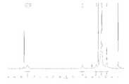
상기 화학식 1-1의 화합물의1H NMR을 도 3에 도시하였다.The1 H NMR of the compound of Formula 1-1 is shown in FIG.
실시예 2: 3,3′′′-디도데실-2,2′:5′,2′′:5′′,2′′′-쿼터티오펜과 4,4′′′-디도데실-2,2′:5′,2′′:5′′,2′′′-쿼터티오펜의 랜덤 공중합체의 합성Example 2: 3,3 '"-idodecyl-2,2': 5 ', 2": 5 ", 2" "-quaterthiophene and 4,4" , 2 ': 5', 2 '': 5 '', 2 '' '- Quaterthiophene
[반응식 4][Reaction Scheme 4]

5,5'''-디(트리메틸스탄닐)-3,3′′′-디도데실-2,2′:5′,2′′:5′′,2′′′-쿼터티오펜 (5,5'''-di(trimethylstannyl)-3,3′′′-didodecyl-2,2′:5′,2′′:5′′,2′′′-quaterthiophene) (0.3 mmol)과 5,5'''-디브로모-4,4′′′-디도데실-2,2′:5′,2′′:5′′,2′′′-쿼터티오펜(5,5'''-dibromo-4,4′′′-didodecyl-2,2′:5′,2′′:5′′,2′′′-quaterthiophene)(0.15 mmol)과 5,5'''-디브로모-3,3′′′-디도데실-2,2′:5′,2′′:5′′,2′′′-쿼터티오펜(5,5'''-dibromo-4,4′′′-didodecyl-2,2′:5′,2′′:5′′,2′′′-quaterthiophene)(0.15 mmol)을 이용하여 실시예 1과 같은 방법으로 하기 화학식 1-2의 반복단위를 포함하는 고분자 수득하였다(수율: 21%, 수평균분자량 = 88,000)5 '' '- di (trimethylstannyl) -3,3' '' - didodecyl-2,2 ': 5', 2 '': 5 '', 2 ' 5 ', 2' '- quaterthiophene (0.3 mmol) and 5' '' - di (trimethylstannyl) -3,3 '' '- didodecyl-2,2' 5 '' '- dibromo-4,4' '' - didodecyl-2,2 ': 5', 2 '': -dibromo-4,4 '' '- didodecyl-2,2': 5 ', 2' ': 5' ', 2' '' - quaterthiophene (0.15 mmol) and 5,5 ' 3,3 '' '- didodecyl-2,2': 5 ', 2' ': 5' ', 2'''-quaterthiophene (5,5' '- dibromo-4,4' '-Didodecyl-2,2': 5 ', 2' ': 5' ', 2' '' - quaterthiophene (0.15 mmol) (Yield: 21%, number average molecular weight = 88,000)
[화학식 1-4][Formula 1-4]

상기 화학식 1-4에서 Dod는 도데실을 의미한다.In the above Formulas 1-4, Dod means dodecyl.
상기 화학식 1-4의 화합물의1H NMR을 도 4에 도시하였다.The1 H NMR of the compound of Formula 1-4 is shown in FIG.
실시예 3: 유기 박막 트랜지스터(OTFT)의 제작Example 3: Fabrication of organic thin film transistor (OTFT)
먼저 세정된 유리기판(12)에 게이트 전극(14)으로 사용되는 크롬을 스퍼터링법으로 1000Å 증착한 후 절연층(16)으로 사용되는 SiO2를 CVD법으로 3000Å 증착하였다. 그 위에 사용되는 Au를 스퍼터링법으로 700Å 증착하여 소스 전극(17a) 및 드레인 전극(17b)을 형성하였다. 유리기판(12)은 유기반도체 재료를 도포하기 전이소프로필 알코올을 이용하여 10분간 세척하여 건조한 후 사용하였다. 또한 절연층으로 사용되는 SiO2의 표면을 개질하기 전 UV/O3을 30분 동안 처리하였다. 이후 소자를 n-헥산에 10mM 농도로 희석시킨 옥틸트리클로로실란 용액에 30분간 담구었다가 헥산 및 알코올로 세척 후 건조시킨 다음 상기 실시예 1에서 합성한 고분자를 클로로벤젠에 1.0 중량% 농도로 용해시켜 스핀-코팅법으로 도포하여 질소 분위기 하에서 150℃에서, 1 시간 동안 베이킹하여 활성층(18)을 형성함으로써 도 1에 도시된 구조의 OTFT 소자(10)를 제작하였다.First, chromium used as the
실시예 4: 유기 박막 트랜지스터(OTFT)의 제작Example 4: Fabrication of organic thin film transistor (OTFT)
실시예 1에서 합성한 고분자 대신 실시예 2에서 합성한 고분자를 사용한 것을 제외하고 상기 실시예 3과 동일한 방법으로 도 1에 도시된 구조의 OTFT 소자(10)를 제작하였다.An
비교예 1: 유기 박막 트랜지스터(OTFT)의 제작Comparative Example 1: Fabrication of organic thin film transistor (OTFT)
하기 화학식 10의 반복단위를 포함하는 고분자(수평균분자량: 63,000)를 사용하는 것을 제외하고는 실시예 3과 동일한 방법으로 OTFT 소자를 제조하였다.An OTFT device was fabricated in the same manner as in Example 3, except that a polymer (number average molecular weight: 63,000) containing a repeating unit represented by the following formula (10) was used.
[화학식 10][Chemical formula 10]

상기 화학식 10에서 Dod는 도데실기를 의미한다.In the above formula (10), Dod means a dodecyl group.
전기적 안정성 비교Electrical Stability Comparison
실시예 3, 실시예 4 및 비교예 1 에서 제조된 OTFT 소자에 대해 KEITHLEY사의 Semiconductor Characterization System(4200-SCS)를 이용하여 전류전달특성 곡선을 측정한 후, 각각 도 5, 도 6 및 도 7에 나타내었고, 이에 따른 전기적 특성을 표 1에 나타내었다. Current transmission characteristic curves of the OTFT devices manufactured in Examples 3 and 4 and Comparative Example 1 were measured using a Semiconductor Characterization System (4200-SCS) manufactured by KEITHLEY Co., and the results are shown in FIGS. 5, 6, and 7 And the electrical characteristics thereof are shown in Table 1. < tb > < TABLE >
[표 1][Table 1]
상기 표 1에서 전하 이동도는 하기 포화영역(saturation region) 전류식인 수학식 1로부터 (ISD)1/2과 VG 를 변수로 한 그래프를 얻고 그 기울기로부터 구하였다.In Table 1, the charge mobility is obtained from the slope by obtaining a graph of (ISD)1/2 and VG as a variable from Equation 1, which is a saturation region current equation.
[수학식 1][Equation 1]

상기 수학식 1에서, ISD는 소스-드레인 전류이고, μ 또는 μFET는 전하 이동도며, CO는 산화막 정전용량이고, W는 채널 폭이고, L은 채널 길이이고, VG는 게이트 전압이며, VT는 문턱전압이다.Where W is the channel width, L is the channel length, VG is the gate voltage, and V L is the channel length. In this equation, ISD is the source-drain current, μ or μFET is the charge transfer, CO is the oxide film capacitance, And VT is the threshold voltage.
전류점멸비(Ion/Ioff)는 온 상태의 최대 전류값(Ion)과 오프 상태의 최소 전류값(Ioff)의 비로 구하였다.The current flicker ratio (Ion / Ioff ) was determined by the ratio of the maximum current value (Ion ) in theon state to the minimum current value (Ioff ) in the off state.
상기 표 1에서 알 수 있는 바와 같이, 실시예 3 및 실시예 4의 고분자를 포 함하는 소자는 비교예 1의 고분자를 포함하는 소자에 비하여 전하 이동도가 2.6 배 이상 높았다.As can be seen from the above Table 1, the devices including the polymers of Examples 3 and 4 had a charge mobility higher than that of the device including the polymer of Comparative Example 1 by 2.6 times or more.
본 발명은 상기 실시예들에 한정되는 것이 아니라 서로 다른 다양한 형태로 제조될 수 있으며, 본 발명이 속하는 기술분야에서 통상의 지식을 가진 자는 본 발명의 기술적 사상이나 필수적인 특징을 변경하지 않고서 다른 구체적인 형태로 실시될 수 있다는 것을 이해할 수 있을 것이다. 그러므로 이상에서 기술한 실시예들은 모든 면에서 예시적인 것이며 한정적이 아닌 것으로 이해해야만 한다.It will be understood by those skilled in the art that various changes in form and details may be made therein without departing from the spirit and scope of the present invention as defined by the following claims. As will be understood by those skilled in the art. It is therefore to be understood that the above-described embodiments are illustrative in all aspects and not restrictive.
도 1은 본 발명의 일 구현예에 따른 트랜지스터의 개략적인 단면도이다.1 is a schematic cross-sectional view of a transistor according to an embodiment of the present invention.
도 2는 본 발명의 다른 일 구현예에 따른 트랜지스터의 개략적인 단면도이다.2 is a schematic cross-sectional view of a transistor according to another embodiment of the present invention.
도 3은 본 발명의 실시예 1에서 합성된 고분자의1H NMR 그래프이다.3 is a1 H NMR graph of a polymer synthesized in Example 1 of the present invention.
도 4는 본 발명의 실시예 2에서 합성된 고분자의1H NMR 그래프이다.4 is a1 H NMR graph of the polymer synthesized in Example 2 of the present invention.
도 5는 본 발명의 실시예 3에 따라 제조된 유기 박막 트랜지스터(OTFT) 소자의 전류전달특성을 측정한 결과를 보인 그래프이다.FIG. 5 is a graph showing a result of measuring a current transfer characteristic of an organic thin film transistor (OTFT) device manufactured according to the third embodiment of the present invention.
도 6은 본 발명의 실시예 4에 따라 제조된 유기 박막 트랜지스터(OTFT) 소자의 전류전달특성을 측정한 결과를 보인 그래프이다.FIG. 6 is a graph showing a result of measuring a current transfer characteristic of an organic thin film transistor (OTFT) device manufactured according to Embodiment 4 of the present invention.
도 7은 비교예 1에 따라 제조된 유기 박막 트랜지스터(OTFT) 소자의 전류전달특성을 측정한 결과를 보인 그래프이다.FIG. 7 is a graph showing a result of measuring current transfer characteristics of an organic thin film transistor (OTFT) device manufactured according to Comparative Example 1. FIG.
<도면의 주요 부분에 대한 부호의 설명>Description of the Related Art
10, 20: 트랜지스터 12, 22: 기판10, 20:
16, 26: 절연층 18, 28: 활성층16, 26: insulating
14, 24: 게이트 전극 17a, 27a: 소스 전극14, 24:
17b, 27b: 드레인 전극17b, 27b: drain electrode
Claims (10)
Translated fromKorean


Priority Applications (2)
| Application Number | Priority Date | Filing Date | Title |
|---|---|---|---|
| KR1020090078971AKR101644048B1 (en) | 2009-08-25 | 2009-08-25 | Organic semiconductor polymer, and transistor including the same |
| US12/662,843US8405071B2 (en) | 2009-08-25 | 2010-05-06 | Organic semiconductor polymer and transistor including the same |
Applications Claiming Priority (1)
| Application Number | Priority Date | Filing Date | Title |
|---|---|---|---|
| KR1020090078971AKR101644048B1 (en) | 2009-08-25 | 2009-08-25 | Organic semiconductor polymer, and transistor including the same |
Publications (2)
| Publication Number | Publication Date |
|---|---|
| KR20110021275A KR20110021275A (en) | 2011-03-04 |
| KR101644048B1true KR101644048B1 (en) | 2016-07-29 |
Family
ID=43623486
Family Applications (1)
| Application Number | Title | Priority Date | Filing Date |
|---|---|---|---|
| KR1020090078971AActiveKR101644048B1 (en) | 2009-08-25 | 2009-08-25 | Organic semiconductor polymer, and transistor including the same |
Country Status (2)
| Country | Link |
|---|---|
| US (1) | US8405071B2 (en) |
| KR (1) | KR101644048B1 (en) |
Families Citing this family (2)
| Publication number | Priority date | Publication date | Assignee | Title |
|---|---|---|---|---|
| KR20130137851A (en) | 2012-06-08 | 2013-12-18 | 삼성디스플레이 주식회사 | Precursor composition for oxide semiconductor, thin film transistor array panel including oxide semiconductor, and manufacturing method of thin film transistor array panel including oxide semiconductor |
| KR102319360B1 (en) | 2017-09-28 | 2021-10-29 | 주식회사 엘지화학 | Electrochromic complex, electrochromic device containing the same and manufacturing method of the electrochromic device |
Citations (4)
| Publication number | Priority date | Publication date | Assignee | Title |
|---|---|---|---|---|
| JP2003221434A (en) | 2002-01-11 | 2003-08-05 | Xerox Corp | Polythiophenes and their preparation |
| JP2003264327A (en) | 2002-01-11 | 2003-09-19 | Xerox Corp | Devices using polythiophenes |
| JP2003261655A (en)* | 2002-01-11 | 2003-09-19 | Xerox Corp | Polythiophenes and devices using the same |
| WO2005122277A1 (en) | 2004-06-10 | 2005-12-22 | Konica Minolta Holdings, Inc. | Organic thin film transistor |
Family Cites Families (7)
| Publication number | Priority date | Publication date | Assignee | Title |
|---|---|---|---|---|
| US5946551A (en)* | 1997-03-25 | 1999-08-31 | Dimitrakopoulos; Christos Dimitrios | Fabrication of thin film effect transistor comprising an organic semiconductor and chemical solution deposited metal oxide gate dielectric |
| US6215130B1 (en)* | 1998-08-20 | 2001-04-10 | Lucent Technologies Inc. | Thin film transistors |
| US6166172A (en)* | 1999-02-10 | 2000-12-26 | Carnegie Mellon University | Method of forming poly-(3-substituted) thiophenes |
| US6949762B2 (en)* | 2002-01-11 | 2005-09-27 | Xerox Corporation | Polythiophenes and devices thereof |
| US6872801B2 (en)* | 2002-01-11 | 2005-03-29 | Xerox Corporation | Polythiophenes and devices thereof |
| US6897284B2 (en)* | 2003-03-19 | 2005-05-24 | Xerox Corporation | Polythiophenes and devices thereof |
| US7837903B2 (en)* | 2008-12-10 | 2010-11-23 | Xerox Corporation | Polythiophenes and electronic devices comprising the same |
- 2009
- 2009-08-25KRKR1020090078971Apatent/KR101644048B1/enactiveActive
- 2010
- 2010-05-06USUS12/662,843patent/US8405071B2/enactiveActive
Patent Citations (4)
| Publication number | Priority date | Publication date | Assignee | Title |
|---|---|---|---|---|
| JP2003221434A (en) | 2002-01-11 | 2003-08-05 | Xerox Corp | Polythiophenes and their preparation |
| JP2003264327A (en) | 2002-01-11 | 2003-09-19 | Xerox Corp | Devices using polythiophenes |
| JP2003261655A (en)* | 2002-01-11 | 2003-09-19 | Xerox Corp | Polythiophenes and devices using the same |
| WO2005122277A1 (en) | 2004-06-10 | 2005-12-22 | Konica Minolta Holdings, Inc. | Organic thin film transistor |
Also Published As
| Publication number | Publication date |
|---|---|
| US20110049480A1 (en) | 2011-03-03 |
| US8405071B2 (en) | 2013-03-26 |
| KR20110021275A (en) | 2011-03-04 |
Similar Documents
| Publication | Publication Date | Title |
|---|---|---|
| KR101314931B1 (en) | Organic Polymeric Semiconductor, Method for preparing thereof and Ambipolar Organic Thin Film Transistor using the same | |
| KR101069519B1 (en) | Organic semiconducting polymer comprising oligothiophene and n-type aromatic compound alternately in the main chain | |
| KR101224708B1 (en) | (Oligothiophene-Arylene) derivatives and Organic Thin Film Transistor using the same | |
| KR101648072B1 (en) | Organic semiconductor polymer, and transistor including the same | |
| KR101151082B1 (en) | Star-shaped (Oligothiophene-Arylene) derivatives and Organic Thin Film Transistor using the same | |
| KR101843550B1 (en) | Organic semiconductor compound, and transistor and electronic device including the same | |
| KR101450137B1 (en) | Copolymer for organic semiconductor and organic thin film transistor and organic electronic device using same | |
| KR101888617B1 (en) | Organic Semiconductor Compound, Organic Thin Film Including the Organic Semiconductor Compound Electronic Device Including the Organic Thin Film and Method of Manufacturing the Organic Thin Film | |
| KR101644048B1 (en) | Organic semiconductor polymer, and transistor including the same | |
| KR20120079423A (en) | Organic semiconductor compound having low band-gap, and transistor and electronic device including the same | |
| EP1953155B1 (en) | Composition containing thiazole rings, organic semiconductor polymer containing the composition, organic active layer containing the organic semiconductor polymer, organic thin film transistor containing the organic active layer, electronic device containing the organic thin film transistor and method of preparing the same | |
| KR101661914B1 (en) | organinc semiconductor compound, manufacturing method therof and organic thin film transistor having them | |
| KR101935466B1 (en) | Organic Electronic Device | |
| KR20130085860A (en) | Organic electronic devices | |
| KR101675073B1 (en) | Organic semiconductor polymer, and transistor and electronic device including the same | |
| KR101730617B1 (en) | Organic semiconductor composition, and transistor and electronic device including polymer therefrom | |
| KR101947020B1 (en) | Organic semiconductor compound having low band-gap, and transistor and electronic device including the same |
Legal Events
| Date | Code | Title | Description |
|---|---|---|---|
| PA0109 | Patent application | Patent event code:PA01091R01D Comment text:Patent Application Patent event date:20090825 | |
| PG1501 | Laying open of application | ||
| A201 | Request for examination | ||
| PA0201 | Request for examination | Patent event code:PA02012R01D Patent event date:20140822 Comment text:Request for Examination of Application Patent event code:PA02011R01I Patent event date:20090825 Comment text:Patent Application | |
| E902 | Notification of reason for refusal | ||
| PE0902 | Notice of grounds for rejection | Comment text:Notification of reason for refusal Patent event date:20150922 Patent event code:PE09021S01D | |
| AMND | Amendment | ||
| E601 | Decision to refuse application | ||
| PE0601 | Decision on rejection of patent | Patent event date:20160426 Comment text:Decision to Refuse Application Patent event code:PE06012S01D Patent event date:20150922 Comment text:Notification of reason for refusal Patent event code:PE06011S01I | |
| AMND | Amendment | ||
| PX0901 | Re-examination | Patent event code:PX09011S01I Patent event date:20160426 Comment text:Decision to Refuse Application Patent event code:PX09012R01I Patent event date:20151222 Comment text:Amendment to Specification, etc. | |
| PX0701 | Decision of registration after re-examination | Patent event date:20160621 Comment text:Decision to Grant Registration Patent event code:PX07013S01D Patent event date:20160525 Comment text:Amendment to Specification, etc. Patent event code:PX07012R01I Patent event date:20160426 Comment text:Decision to Refuse Application Patent event code:PX07011S01I Patent event date:20151222 Comment text:Amendment to Specification, etc. Patent event code:PX07012R01I | |
| X701 | Decision to grant (after re-examination) | ||
| GRNT | Written decision to grant | ||
| PR0701 | Registration of establishment | Comment text:Registration of Establishment Patent event date:20160725 Patent event code:PR07011E01D | |
| PR1002 | Payment of registration fee | Payment date:20160725 End annual number:3 Start annual number:1 | |
| PG1601 | Publication of registration | ||
| FPAY | Annual fee payment | Payment date:20190619 Year of fee payment:4 | |
| PR1001 | Payment of annual fee | Payment date:20190619 Start annual number:4 End annual number:4 | |
| PR1001 | Payment of annual fee | Payment date:20200616 Start annual number:5 End annual number:5 | |
| PR1001 | Payment of annual fee | Payment date:20210621 Start annual number:6 End annual number:6 | |
| PR1001 | Payment of annual fee | Payment date:20220615 Start annual number:7 End annual number:7 | |
| PR1001 | Payment of annual fee | Payment date:20250612 Start annual number:10 End annual number:10 |