KR101643376B1 - Remote touch panel using light sensor and remote touch screen apparatus having the same - Google Patents
Remote touch panel using light sensor and remote touch screen apparatus having the sameDownload PDFInfo
- Publication number
- KR101643376B1 KR101643376B1KR1020100030509AKR20100030509AKR101643376B1KR 101643376 B1KR101643376 B1KR 101643376B1KR 1020100030509 AKR1020100030509 AKR 1020100030509AKR 20100030509 AKR20100030509 AKR 20100030509AKR 101643376 B1KR101643376 B1KR 101643376B1
- Authority
- KR
- South Korea
- Prior art keywords
- electrode
- semiconductor layer
- light
- contact
- touch panel
- Prior art date
- Legal status (The legal status is an assumption and is not a legal conclusion. Google has not performed a legal analysis and makes no representation as to the accuracy of the status listed.)
- Active
Links
Images


Classifications
- G—PHYSICS
- G06—COMPUTING OR CALCULATING; COUNTING
- G06F—ELECTRIC DIGITAL DATA PROCESSING
- G06F3/00—Input arrangements for transferring data to be processed into a form capable of being handled by the computer; Output arrangements for transferring data from processing unit to output unit, e.g. interface arrangements
- G06F3/01—Input arrangements or combined input and output arrangements for interaction between user and computer
- G06F3/03—Arrangements for converting the position or the displacement of a member into a coded form
- G06F3/041—Digitisers, e.g. for touch screens or touch pads, characterised by the transducing means
- G06F3/042—Digitisers, e.g. for touch screens or touch pads, characterised by the transducing means by opto-electronic means
- G06F3/0421—Digitisers, e.g. for touch screens or touch pads, characterised by the transducing means by opto-electronic means by interrupting or reflecting a light beam, e.g. optical touch-screen
- G—PHYSICS
- G06—COMPUTING OR CALCULATING; COUNTING
- G06F—ELECTRIC DIGITAL DATA PROCESSING
- G06F3/00—Input arrangements for transferring data to be processed into a form capable of being handled by the computer; Output arrangements for transferring data from processing unit to output unit, e.g. interface arrangements
- G06F3/01—Input arrangements or combined input and output arrangements for interaction between user and computer
- G06F3/03—Arrangements for converting the position or the displacement of a member into a coded form
- G06F3/033—Pointing devices displaced or positioned by the user, e.g. mice, trackballs, pens or joysticks; Accessories therefor
- G06F3/038—Control and interface arrangements therefor, e.g. drivers or device-embedded control circuitry
- G06F3/0386—Control and interface arrangements therefor, e.g. drivers or device-embedded control circuitry for light pen
- G—PHYSICS
- G06—COMPUTING OR CALCULATING; COUNTING
- G06F—ELECTRIC DIGITAL DATA PROCESSING
- G06F3/00—Input arrangements for transferring data to be processed into a form capable of being handled by the computer; Output arrangements for transferring data from processing unit to output unit, e.g. interface arrangements
- G06F3/01—Input arrangements or combined input and output arrangements for interaction between user and computer
- G06F3/03—Arrangements for converting the position or the displacement of a member into a coded form
- G06F3/041—Digitisers, e.g. for touch screens or touch pads, characterised by the transducing means
- G06F3/0412—Digitisers structurally integrated in a display
- G—PHYSICS
- G06—COMPUTING OR CALCULATING; COUNTING
- G06F—ELECTRIC DIGITAL DATA PROCESSING
- G06F3/00—Input arrangements for transferring data to be processed into a form capable of being handled by the computer; Output arrangements for transferring data from processing unit to output unit, e.g. interface arrangements
- G06F3/01—Input arrangements or combined input and output arrangements for interaction between user and computer
- G06F3/03—Arrangements for converting the position or the displacement of a member into a coded form
- G06F3/041—Digitisers, e.g. for touch screens or touch pads, characterised by the transducing means
- G06F3/042—Digitisers, e.g. for touch screens or touch pads, characterised by the transducing means by opto-electronic means
Landscapes
- Engineering & Computer Science (AREA)
- General Engineering & Computer Science (AREA)
- Theoretical Computer Science (AREA)
- Human Computer Interaction (AREA)
- Physics & Mathematics (AREA)
- General Physics & Mathematics (AREA)
- Position Input By Displaying (AREA)
Abstract
Translated fromKoreanDescription
Translated fromKorean광센서를 이용한 리모트 터치 패널(remote touch panel) 및 이를 구비하는 리모트 터치 스크린 장치를 개시한다. 더욱 상세하게는, 광센서로서 광민감성 산화물 반도체(light-sensitive oxide semiconductor)를 이용한 리모트 터치 패널 및 이를 구비하는 리모트 터치 스크린 장치를 개시한다.A remote touch panel using an optical sensor and a remote touch screen device having the remote touch panel are disclosed. More particularly, the present invention relates to a remote touch panel using a light-sensitive oxide semiconductor as a photosensor and a remote touch screen device having the same.
일반적으로, 터치 스크린이란 키보드를 사용하지 않고 화면에 나타난 문자나 특정 위치에 사람의 손 또는 물체가 닿으면 그 위치를 파악하여 소프트웨어에 의해 특정 처리를 할 수 있도록, 화면에서 직접 입력 자료를 받을 수 있게 만든 화면을 말한다. 이를 위하여, 터치 스크린은 일반 모니터의 화면에 터치 패널이라는 장치를 덧붙여서 그 기능을 발휘하도록 한다. 터치 패널은 키보드나 마우스를 대신하는 입력 장치로서, 디스플레이의 표면에 장착되어 사용자가 디스플레이에 표시되는 화면을 눈으로 보면서 일정 위치를 직접 눌러 대화하는 식으로 여러 가지의 입력 조작을 할 수 있도록 한 장치이다. 터치 패널은 키보드가 필요 없고 조작이 간단하기 때문에 기존의 키보드 및 마우스와 함께, 컴퓨터 시스템의 기본적인 입력 장치 중 하나로서 점차 사용이 증가하고 있다.Generally, a touch screen is a touch screen that can receive input data directly from the screen so that the software can recognize the position of the touch screen when a human hand or an object touches a character or a specific position on the screen without using a keyboard It is the screen which made it. To this end, a touch screen is used to add a device called a touch panel to the screen of a general monitor, thereby exercising its function. A touch panel is an input device that replaces a keyboard or a mouse and is mounted on a surface of a display so that a user can perform various input operations by directly touching a predetermined position while viewing the screen displayed on the display, to be. Since the touch panel does not require a keyboard and is simple to operate, its use is gradually increasing as one of the basic input devices of a computer system together with a conventional keyboard and mouse.
이러한 터치 패널에는 압력식 저항막 방식, 접촉식 정전용량 방식, 표면초음파전도(Surface Acoustic Wave; SAW) 방식, 적외선광 감지 방식 및 압전 방식 등의 다양한 종류가 있다. 이들 중에서, 터치 스크린에는 광투과율이 높고 반응속도가 빠르며 내성이 우수하여 작동 환경의 영향을 적게 받는 압력식 저항막 방식의 터치 패널이 일반적으로 가장 많이 채용되고 있다. 이렇게 기술의 발전에 따라 다양한 방식으로 터치 패널이 구현되고 있으며, 이에 따라 그 가격이 저렴해지면서 점차 그 사용이 일반화되고 있다. 또한, 단순히 하나의 접촉점만을 인식하는 것이 아니라 다수의 접촉점을 인식할 수 있는 멀티-터치(Multi-touch)를 통해 보다 다양하고 자연스러운 조작이 가능하게 되었다.Such a touch panel includes various types such as a pressure resistive film type, a contact type capacitance type, a surface acoustic wave (SAW) type, an infrared light sensing type, and a piezoelectric type. Of these, a pressure resistive film type touch panel, which has a high light transmittance, a high reaction speed and a high resistance, and is less influenced by the operating environment, is generally employed most as a touch screen. In accordance with the development of the technology, the touch panel is implemented in various ways, and as the price is lowered, the use thereof is gradually becoming common. In addition, it is possible to perform more various and natural operations through multi-touch which can recognize not only one contact point but also many contact points.
그러나, 지금까지 사용되고 있는 터치 패널은 손이나 펜 등을 이용하여 패널에 직접 터치를 해야만 하는 방식이다. 따라서, 가장 널리 사용되는 압력식 저항막 방식의 터치 패널은 외부 압력에 의해 상부/하부 도전층이 손상되는 문제가 발생할 수도 있다. 또한, 이러한 방식은 센싱 효과가 우수할 수는 있지만, 패널과 사용자 사이가 가까워야 한다. 따라서, 터치 패널은 일반적인 테스크탑 컴퓨터, 노트북 컴퓨터, 또는 핸드폰이나 네비게이션과 같은 휴대용 장치 등의 소형 또는 중형 디스플레이에서만 사용이 가능하다. 그러나, 디스플레이가 점차 대형화되면서 사용자와 디스플레이 사이의 거리가 멀어지는 경우에는 터치 패널을 적용하기가 어려울 수도 있다. 최근에는 사용자의 음성이나 동작(gesture)를 원격으로 인식하는 방식의 패널도 제안되고 있으나, 대형 디스플레이에 적용하기는 아직까지 실용화에 한계가 있다.However, the touch panel that has been used so far requires a touch directly to the panel using a hand or a pen. Therefore, the most widely used pressure type resistive touch panel may cause damage to the upper / lower conductive layer due to external pressure. In addition, this method may have a good sensing effect, but should be close to the panel and the user. Accordingly, the touch panel can be used only on a small or medium-sized display such as a general desktop computer, a notebook computer, or a portable device such as a mobile phone or a navigation device. However, if the distance between the user and the display increases as the display becomes larger and larger, it may be difficult to apply the touch panel. In recent years, a panel for remotely recognizing a user's voice or gesture has been proposed, but application to a large-sized display still has limitations in practical use.
광센서를 이용하여 대형 디스플레이를 원거리에서 조작할 수 있는 리모트 터치 패널을 제공한다.Provided is a remote touch panel capable of operating a large display at a distance using an optical sensor.
또한, 이러한 리모트 터치 패널을 구비하는 리모트 터치 스크린 장치를 제공한다.Further, a remote touch screen device having such a remote touch panel is provided.
개시된 본 발명의 일 유형에 따른 리모트 터치 패널은 2차원 배열되어 있는 다수의 광센서 셀들을 포함하며, 각각의 광센서 셀은 광민감성 반도체층; 및 상기 광민감성 반도체층과 전기적으로 연결된 제 1 전극 및 제 2 전극을 포함할 수 있다.According to a first aspect of the present invention, a remote touch panel includes a plurality of optical sensor cells arranged two-dimensionally, each optical sensor cell including a light-sensitive semiconductor layer; And a first electrode and a second electrode electrically connected to the light-sensitive semiconductor layer.
여기서, 상기 광민감성 반도체층은 광민감성 산화물 반도체 재료로 이루어질 수 있다.Here, the light-sensitive semiconductor layer may be made of a photosensitive silicon oxide semiconductor material.
또한, 상기 광민감성 산화물 반도체 재료는 가시광선을 통과시키며 400nm 이하의 파장을 갖는 광을 흡수하여 전자와 홀을 생성시키는 산화물 반도체 재료일 수 있다.The light-sensitive oxide semiconductor material may be an oxide semiconductor material that transmits visible light and absorbs light having a wavelength of 400 nm or less to generate electrons and holes.
예컨대, 상기 광민감성 산화물 반도체 재료는 ZnOx, doped-ZnOx 또는 InZnO일 수 있다.For example, the light-sensitive oxide semiconductor material may be ZnOx , doped-ZnOx, or InZnO.
상기 광민감성 반도체층은 각각의 광센서 셀마다 하나씩 배치된 다수의 광민감성 반도체 셀들로 분할될 수 있으며, 다수의 평행한 제 1 전극들이 상기 다수의 광민감성 반도체 셀들에 걸쳐 제 1 방향을 따라 연장될 수 있고, 다수의 평행한 제 2 전극들이 상기 다수의 광민감성 반도체 셀들에 걸쳐 상기 제 1 방향과 수직한 제 2 방향을 따라 연장될 수 있다.The photo-sensitive semiconductor layer may be divided into a plurality of photo-sensitive semiconductor cells arranged one for each optical sensor cell, and a plurality of parallel first electrodes extend along the first direction across the plurality of photo- And a plurality of parallel second electrodes may extend along a second direction perpendicular to the first direction across the plurality of photo sensitive semiconductor cells.
또한, 상기 리모트 터치 패널은, 상기 제 1 전극과 광민감성 반도체층을 전기적으로 연결시키도록 배치된 제 1 컨택; 및 상기 제 2 전극과 광민감성 반도체층을 전기적으로 연결시키도록 배치된 제 2 컨택을 더 포함하며, 상기 제 1 컨택과 제 2 컨택은 각각의 광센서 셀마다 하나씩 배치될 수 있다.The remote touch panel may further include: a first contact arranged to electrically connect the first electrode and the photosensitive semiconductor layer; And a second contact arranged to electrically connect the second electrode and the photosensitive semiconductor layer, wherein the first contact and the second contact may be disposed one by one for each optical sensor cell.
여기서, 상기 제 1 컨택의 일부와 제 2 컨택의 일부가 각각 제 1 전극과 제 2 전극으로부터 수직한 방향으로 연장되어 돌출될 수 있다.Here, a part of the first contact and a part of the second contact may protrude from the first electrode and the second electrode in the vertical direction, respectively.
한편, 다수의 광센서 셀들이 한 장의 광민감성 반도체층을 공유할 수도 있으며, 다수의 평행한 제 1 전극들이 상기 광민감성 반도체층에 걸쳐 제 1 방향을 따라 연장될 수 있고, 다수의 평행한 제 2 전극들이 상기 광민감성 반도체층에 걸쳐 상기 제 1 방향과 수직한 제 2 방향을 따라 연장될 수 있다.Alternatively, a plurality of optical sensor cells may share a single photosensitive semiconductor layer, a plurality of parallel first electrodes may extend along the first direction across the photosensitive semiconductor layer, and a plurality of parallel Two electrodes may extend along a second direction perpendicular to the first direction across the photosensitive semiconductor layer.
상기 리모트 터치 패널은, 상기 제 1 및 제 2 전극들을 덮도록 상기 광민감성 반도체층의 표면 위에 전체적으로 채워져 있는 투명 절연층을 더 포함할 수 있으며, 상기 제 1 전극과 제 2 전극은 광민감성 반도체층의 동일한 표면 위로 서로 접촉하지 않고 교차할 수 있다.The remote touch panel may further include a transparent insulation layer that is formed on the surface of the photosensitive semiconductor layer so as to cover the first and second electrodes. The first electrode and the second electrode may include a light- Without touching each other on the same surface of the substrate.
또한, 상기 리모트 터치 패널은, 상기 제 1 전극과 광민감성 반도체층을 전기적으로 연결시키도록 배치된 제 1 컨택; 및 상기 제 1 및 제 2 전극들을 덮도록 상기 광민감성 반도체층의 표면 위에 전체적으로 채워져 있는 투명 절연층을 더 포함할 수 있으며, 상기 제 2 전극은 상기 광민감성 반도체층의 표면 위에 직접 접촉하여 배치되고, 상기 제 1 전극과 제 2 전극은 광민감성 반도체층의 동일한 표면 위로 서로 접촉하지 않고 교차할 수 있다.The remote touch panel may further include: a first contact arranged to electrically connect the first electrode and the photosensitive semiconductor layer; And a transparent insulating layer that is entirely filled on the surface of the photosensitive semiconductor layer to cover the first and second electrodes, and the second electrode is disposed in direct contact with the surface of the photosensitive semiconductor layer , The first electrode and the second electrode may cross without contacting each other over the same surface of the photosensitive semiconductor layer.
또한, 상기 리모트 터치 패널은, 상기 제 1 전극과 광민감성 반도체층을 전기적으로 연결시키도록 배치된 제 1 컨택; 및 상기 제 1 전극 및 제 1 컨택을 덮도록 상기 광민감성 반도체층의 한 표면 위에 전체적으로 채워져 있는 투명 절연층을 더 포함할 수 있으며, 상기 제 2 전극은 상기 광민감성 반도체층의 반대쪽 표면 위에 직접 접촉하여 배치될 수 있다.The remote touch panel may further include: a first contact arranged to electrically connect the first electrode and the photosensitive semiconductor layer; And a transparent insulating layer that is entirely filled on one surface of the photosensitive semiconductor layer so as to cover the first electrode and the first contact, and the second electrode may be in direct contact with the opposite surface of the photosensitive semiconductor layer, .
상기 제 1 전극은 상기 광민감성 반도체층의 한 표면 위에 직접 접촉하여 배치되며, 상기 제 2 전극은 상기 광민감성 반도체층의 반대쪽 표면 위에 직접 접촉하여 배치될 수 있다.The first electrode is disposed in direct contact with one surface of the photosensitive semiconductor layer, and the second electrode is disposed in direct contact with the opposite surface of the photosensitive semiconductor layer.
상기 제 1 전극과 제 2 전극 중 적어도 하나는 각각의 광센서 셀 영역마다 적어도 하나씩 원형, 타원형 또는 다각형 형태의 패턴을 가질 수 있다.At least one of the first electrode and the second electrode may have a circular, elliptical or polygonal pattern in each of the optical sensor cell regions.
한편, 다수의 광센서 셀들이 한 장의 광민감성 반도체층을 공유할 수도 있으며, 상기 제 1 전극은 각각의 광센서 셀 영역마다 적어도 하나의 원형, 타원형 또는 다각형 형태의 패턴을 갖도록 상기 광민감성 반도체층의 한 표면 위에 배치되고, 상기 제 2 전극은 상기 광민감성 반도체층의 반대쪽 표면 전체 영역에 걸쳐서 패턴이 없이 한 층으로 배치될 수 있다.The plurality of photosensor cells may share a light-sensitive semiconductor layer, and the first electrode may have a pattern of at least one circular, elliptic or polygonal shape for each optical sensor cell region, And the second electrode may be disposed in one layer without patterning over the entire area of the surface opposite to the light-sensitive semiconductor layer.
상기 리모트 터치 패널은, 상기 광민감성 반도체층 상의 위치를 정확히 알고 있는 다수의 지점들에 각각 배치된 다수의 전류 감지 센서들을 더 포함할 수 있다.The remote touch panel may further include a plurality of current sensing sensors respectively disposed at a plurality of points that accurately recognize a position on the photosensitive semiconductor layer.
상기 제 1 및 제 2 전극은 투명 전극일 수 있다.The first and second electrodes may be transparent electrodes.
예컨대, 상기 투명 전극은 ITO 또는 IZO로 이루어질 수 있다.For example, the transparent electrode may be made of ITO or IZO.
상기 제 1 전극과 제 2 전극 중에서 양의 전압이 인가되는 양극은 상대적으로 높은 일함수를 갖도록 처리되며, 음극은 상대적으로 낮은 일함수를 갖도록 처리될 수 있다.A positive electrode to which a positive voltage is applied among the first electrode and the second electrode is processed to have a relatively high work function and the negative electrode can be processed to have a relatively low work function.
예컨대, 상대적으로 높은 일함수를 갖는 양극은 4.8~5.2eV의 일함수를 가지며, 상대적으로 낮은 일함수를 갖는 음극은 4.1~4.5eV의 일함수를 가질 수 있다.For example, a cathode having a relatively high work function may have a work function of 4.8 to 5.2 eV, and a cathode having a relatively low work function may have a work function of 4.1 to 4.5 eV.
한편, 본 발명의 다른 유형에 따른 리모트 터치 스크린 장치는, 제 1 항 내지 제 21 항 중 어느 한 항에 따른 리모트 터치 패널; 영상을 디스플레이 하는 디스플레이 장치; 및 상기 리모트 터치 패널에 조사되는 광신호를 제공하는 광원 장치;를 포함할 수 있다.According to another aspect of the present invention, there is provided a remote touch screen device comprising: a remote touch panel according to any one of claims 1 to 21; A display device for displaying an image; And a light source device for providing an optical signal irradiated to the remote touch panel.
상기 디스플레이 장치에서 하나의 화소가 4개의 영역으로 분할될 수 있으며, 상기 4개의 영역 중에서 3개의 영역은 각각 적, 녹, 청색을 위한 RGB 서브화소에 할당되고, 나머지 하나의 영역에는 상기 리모트 터치 패널의 하나의 광센서 셀이 배치될 수 있다.In the display device, one pixel may be divided into four regions, and three of the four regions are allocated to red, green, and blue RGB sub-pixels, One optical sensor cell may be disposed.
예컨대, 상기 리모트 터치 패널에 조사되는 광신호의 변화에 따라, 상기 디스플레이 장치에서 디스플레이 되는 영상의 일부 또는 전체에 대한 이동, 확대, 축소, 숨김, 회전 동작이 수행되거나 특정 메뉴의 선택, 실행, 취소 동작이 수행될 수 있다.For example, a movement, enlargement, reduction, hiding, and rotation operation of a part or all of an image displayed on the display device is performed according to a change of an optical signal irradiated to the remote touch panel, or a selection, execution, An operation can be performed.
상기 광신호의 변화는, 예컨대, 광신호의 크기의 비례적인 확대 또는 축소, 광신호의 이동, 어느 한 방향만으로의 광신호의 확장, 광신호의 모양 변화, 광신호가 입사하는 시간의 변화, 광신호의 광량의 변화, 광신호의 파장의 변화, 소정의 시간 주기 내에서 광신호의 연속적인 입사 횟수의 변화 중에서 어느 하나 또는 이들의 조합을 포함할 수 있다.The change of the optical signal may include, for example, proportional enlargement or reduction of the size of the optical signal, movement of the optical signal, expansion of the optical signal in only one direction, change in shape of the optical signal, A change in the light amount of the signal, a change in the wavelength of the optical signal, and a change in the number of consecutive incidents of the optical signal within a predetermined time period, or a combination thereof.
개시된 리모트 터치 패널은, 손과 펜 등의 직접 터치가 어려운 대형 디스플레이를 원거리에서 터치하듯이 제어할 수 있다. 예를 들어, 레이저 포인터 등과 같은 간단한 광원 장치를 이용하여, 마치 모니터를 보면서 마우스로 컴퓨터를 제어하듯이 대형 디스플레이 장치를 손쉽게 제어할 수 있다.The disclosed remote touch panel can be controlled as if it touches a large display which is difficult to directly touch with hands and pens at a long distance. For example, a simple light source device such as a laser pointer can be used to easily control a large-sized display device as if controlling the computer with a mouse while viewing the monitor.
도 1은 광센서를 이용한 리모트 터치 패널을 사용함으로써 광원 장치로 디스플레이 장치를 원격으로 제어하는 예를 개략적으로 보이는 개념도이다.
도 2는 본 발명의 원리를 설명하기 위한 하나의 광센서의 구조를 개략적으로 도시하는 평면도이다.
도 3은 도 2의 광센서에 광이 조사되는 상태를 개략적으로 도시하는 평면도이다.
도 4는 본 발명의 원리를 설명하기 위한 광센서의 구조를 개략적으로 도시하는 단면도이다.
도 5는 광민감성 산화물 반도체의 파장에 따른 흡수/투과 곡선을 나타내는 그래프이다.
도 6은 광민감성 산화물 반도체를 갖는 광센서를 이용한 리모트 터치 패널의 개략적인 개념도이다.
도 7은 광민감성 산화물 반도체를 갖는 광센서를 이용한 리모트 터치 패널의 예시적인 구조를 개략적으로 보이는 평면도이다.
도 8은 광민감성 산화물 반도체를 갖는 광센서를 이용한 리모트 터치 패널의 다른 예시적인 구조를 개략적으로 보이는 평면도이다.
도 9는 도 8에 도시된 리모트 터치 패널을 디스플레이 장치에 적용한 예에 대한 개략적인 개념도이다.
도 10은 수평 및 수직 전도성 라인들과 제 1 및 제 2 컨택들의 배치 구조 및 하나의 좌표로서 인식되는 광센싱 셀의 영역을 도시한다.
도 11은 도 10의 A-A' 라인에 대한 리모트 터치 패널의 단면을 도시한다.
도 12 내지 도 14는 리모트 터치 패널의 다양한 다른 단면의 예를 개략적으로 도시한다.
도 15는 원형의 패턴을 갖는 수평 전도성 라인을 구비하는 리모트 터치 패널을 도시한다.
도 16은 도 15에 도시된 리모트 터치 패널의 한 광센서 영역에 대한 단면도이다.
도 17은 하나의 대면적 하부 전극 및 패턴을 갖는 상부 전극을 구비하는 리모트 터치 패널을 도시한다.
도 18은 도 17에 도시된 리모트 터치 패널의 한 광센서 영역에 대한 단면도이다.
도 19는 도 17에 도시된 리모트 터치 패널에서 광이 입사한 위치를 감지하는 원리를 설명한다.
도 20a 내지 도 20i는 리모트 터치 패널에 입사할 수 있는 다양한 광신호의 예를 보인다.1 is a conceptual diagram schematically showing an example of remotely controlling a display device by a light source device by using a remote touch panel using an optical sensor.
2 is a plan view schematically showing the structure of one optical sensor for explaining the principle of the present invention.
3 is a plan view schematically showing a state in which light is irradiated to the photosensor of FIG.
4 is a cross-sectional view schematically showing the structure of an optical sensor for explaining the principle of the present invention.
5 is a graph showing the absorption / transmission curve according to the wavelength of the light-sensitive oxide semiconductor.
FIG. 6 is a schematic diagram of a remote touch panel using an optical sensor having a photo-sensitive oxide semiconductor.
7 is a plan view schematically showing an exemplary structure of a remote touch panel using an optical sensor having a photosensitive silicon oxide semiconductor.
8 is a plan view schematically showing another exemplary structure of a remote touch panel using a photosensor having a photo sensitive oxide semiconductor.
FIG. 9 is a schematic diagram illustrating an example in which the remote touch panel shown in FIG. 8 is applied to a display device.
Figure 10 shows the layout of the horizontal and vertical conductive lines and the first and second contacts and the area of the light sensing cell which is recognized as one coordinate.
FIG. 11 shows a cross section of the remote touch panel with respect to line AA 'in FIG.
Figs. 12 to 14 schematically show examples of various other cross-sections of the remote touch panel.
15 shows a remote touch panel having a horizontal conductive line having a circular pattern.
16 is a cross-sectional view of the optical sensor area of the remote touch panel shown in Fig.
17 shows a remote touch panel having one large-area lower electrode and an upper electrode having a pattern.
18 is a cross-sectional view of the optical sensor area of the remote touch panel shown in Fig.
Fig. 19 illustrates a principle of detecting the position of light incident on the remote touch panel shown in Fig.
20A to 20I show examples of various optical signals that can be incident on the remote touch panel.
이하, 첨부된 도면들을 참조하여, 광센서를 이용한 리모트 터치 패널 및 이를 구비하는 리모트 터치 스크린 장치에 대해 상세하게 설명한다. 이하의 도면들에서 동일한 참조부호는 동일한 구성요소를 지칭하며, 도면상에서 각 구성요소의 크기는 설명의 명료성과 편의상 과장되어 있을 수 있다.Hereinafter, a remote touch panel using an optical sensor and a remote touch screen device having the same will be described in detail with reference to the accompanying drawings. In the following drawings, like reference numerals refer to like elements, and the size of each element in the drawings may be exaggerated for clarity and convenience of explanation.
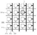
도 1은 리모트 터치 패널을 사용함으로써 광원 장치로 디스플레이 장치를 원격으로 제어하는 예를 개략적으로 보이는 개념도이다. 도 1을 참조하면, 이하에서 설명될 광센서를 이용한 리모트 터치 패널이 적용된 디스플레이 장치(110)를 포함하는 리모트 터치 스크린 장치(100)가 도시되어 있다. 이러한 리모트 터치 스크린 장치(100)에서, 예를 들어, 레이저 포인터와 같은 간단한 광원 장치(120)로 디스플레이 장치(110)에 광을 조사하면, 리모트 터치 패널 내에 배열된 광센서가 광을 인식하게 된다. 리모트 터치 패널 내에는 다수의 광센서 셀들이 2차원 배열되어 있으므로, 광이 조사된 좌표를 특정할 수 있다. 따라서, 마치 손이나 펜으로 터치 스크린을 터치하는 것과 동일한 효과를 얻을 수 있다.1 is a conceptual diagram schematically showing an example of remotely controlling a display device with a light source device by using a remote touch panel. Referring to FIG. 1, a remote
이러한 광센서를 이용한 리모트 터치 패널의 가장 기본이 되는 개념은, 광민감성 반도체에 전기장을 가한 후, 전자와 홀을 생성시킬 정도의 빛에너지를 상기 광민감성 반도체에 가해 광전류(photo current)를 만들어 내는 것이다. 그러면, 이렇게 생성된 광전류를 이용하여 빛이 조사된 위치를 알아낼 수 있다. 즉, 다수의 광센서 셀들 중 어떠한 광센서 셀에서 광전류가 발생하였는 지를 검출하면 빛이 조사된 위치를 특정할 수 있다.The basic concept of a remote touch panel using such a photosensor is that after applying an electric field to a photo-sensitive semiconductor, a photoelectric current is generated by applying light energy enough to generate electrons and holes to the photo- will be. Then, the photocurrent generated in this way can be used to find out the position where the light is irradiated. That is, when the photocurrent is generated in the optical sensor cell among the plurality of optical sensor cells, the location where the light is irradiated can be specified.
도 2는 위와 같은 개념에 기초한 하나의 광센서의 구조를 개략적으로 도시하고 있다. 도 2를 참조하면, 광센서(10)는 광민감성 반도체(11) 위에 배열된 두 개의 전극(12, 13)을 포함한다. 이러한 구조에서, 예를 들어, 제 1 전극(12)을 그라운드에 연결하고, 제 2 전극(13)에 소정의 전압을 제공할 수 있다. 그러면, 광민감성 반도체(11)에 전기장이 인가된다. 그런 후, 도 3에 도시된 바와 같이, 제 1 전극(12)과 제 2 전극(13) 사이의 영역에 걸쳐 광민감성 반도체(11)에 광(L)이 조사되면, 광민감성 반도체(11)에서 광전류가 발생하게 된다. 따라서, 도 4의 단면도에서 화살표로 표시한 바와 같이, 제 2 전극(13)으로부터 광민감성 반도체(11)를 통해 제 1 전극(11)으로 전류가 흐르게 된다.Fig. 2 schematically shows the structure of one optical sensor based on the above concept. Referring to FIG. 2, the
그런데, 광센서(10)를 이용한 터치 패널을 디스플레이 장치(110)에 적용할 경우, 디스플레이 장치(110)에서 발생하는 가시광선 또는 디스플레이 장치(110)의 백라이트 유닛(115, 도 6 참조)에서 발생하는 가시광선으로 인해, 광센서(10)의 감도가 저하될 수 있다. 또한, 광센서(10)로 인해 디스플레이 장치(110)의 휘도가 감소될 수 있다. 따라서, 이러한 점을 고려하여, 광민감성 반도체(11)로서 가시광선에 대한 감도가 작고 가시광선에 대해 높은 투과율을 갖는 재료를 사용할 수 있다. 예를 들어, 넓은 밴드갭(wide bandgap)을 갖는 산화물 반도체는 가시광선을 통과시키며, UV 내지 근청색(near blue)의 광 조사시에 전자와 홀을 생성시킬 수 있다.However, when the touch panel using the
위와 같은 조건을 만족시킬 수 있는 대표적인 광민감성 산화물 반도체로서, 예를 들어 ZnOx, doped-ZnOx 또는 InZnO 등이 있다. 이들 재료들은 약 400nm 이하의 근청색광 또는 UV 광에 의해 조사되면, 전자와 홀을 생성하여 전류가 흐르게 하지만 가시광선에 대해서는 높은 저항 상태를 유지한다. 예를 들어, ZnO의 표면 위에 약 6mm×6mm 크기의 두 알루미늄(Al) 전극을 약 0.1mm 간격으로 형성하고, 상기 전극에 3V의 전압을 인가하면, UV 조사시에는 약 0.17 mA의 전류가 흐르지만, UV가 조사되지 않는 동안에는 약 960 kW의 저항값을 보인다. 또한, 도 5의 그래프를 통해 알 수 있듯이, ZnO는 약 400nm 이상의 파장을 갖는 가시광선은 거의 통과시키지만, 약 400nm 이하의 파장을 갖는 근청색광 또는 UV 광은 거의 흡수하는 성질을 가지고 있다. 따라서 예시된 산화물 반도체 재료들은 상술한 광민감성 반도체(11)의 재료로서 적당하다는 것을 알 수 있다.As typical photo-sensitive oxide semiconductors capable of satisfying the above conditions, for example, there are ZnOx , doped-ZnOx, or InZnO. These materials, when irradiated with near-ultraviolet light or UV light of about 400 nm or less, generate electrons and holes to make electric current flow, but maintain a high resistance state for visible light. For example, when two aluminum (Al) electrodes each having a size of about 6 mm x 6 mm are formed on the surface of ZnO at intervals of about 0.1 mm and a voltage of 3 V is applied to the electrodes, a current of about 0.17 mA However, the resistance value is about 960 kW while UV is not irradiated. As can be seen from the graph of FIG. 5, ZnO almost passes visible light having a wavelength of about 400 nm or more, but almost absorbs near-blue light or UV light having a wavelength of about 400 nm or less. Therefore, it can be seen that the illustrated oxide semiconductor materials are suitable as the material of the above-described
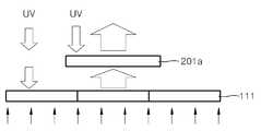
도 6은 위와 같은 광민감성 산화물 반도체를 포함하는 광센서를 이용한 리모트 터치 패널의 개념도를 도시하고 있다. 도 6을 참조하면, 다수의 화소를 갖는 디스플레이 패널(111)과 상기 디스플레이 패널(111)에 가시광선을 제공하는 백라이트 유닛(115)을 포함하는 디스플레이 장치(110) 위로 리모트 터치 패널(200)이 배치되어 있다. 도 6에 도시된 바와 같이, 백라이트 유닛(115)에서 발생한 가시광선은 디스플레이 패널(111)을 통과하면서 소정의 영상을 갖게 된다. 이 소정의 영상을 포함하는 가시광선은 산화물 반도체 재료를 포함하는 리모트 터치 패널(200)에 입사하게 된다. 리모트 터치 패널(200)의 산화물 반도체 재료는, 상술한 바와 같이, 가시광선에 민감하지 않고 가시광선을 투과시키는 성질을 갖는다. 따라서, 소정의 영상을 포함하는 가시광선은 리모트 터치 패널(200)의 동작에 영향을 주지 않고 리모트 터치 패널(200)을 통과할 수 있다.FIG. 6 is a conceptual diagram of a remote touch panel using a photosensor including the above-described photo-sensitive oxide semiconductor. 6, a
한편, 리모트 터치 패널(200)에는 약 400nm 이하의 근청색광 또는 UV 광이 조사된다. 리모트 터치 패널(200)은 이러한 근청색광 또는 UV 광을 감지하여, 터치 패널로서 역할을 하게 된다. 더욱이, 리모트 터치 패널(200)의 산화물 반도체 재료는 약 400nm 이하의 파장을 갖는 광을 흡수하는 성질을 갖기 때문에, 리모트 터치 패널(200)에 조사되는 근청색광 또는 UV 광은 디스플레이 장치(110)에 도달하지 않는다. 일반적으로, 비교적 높은 에너지를 갖는 UV 광이 디스플레이 장치(110)에 입사하면, 박막 트랜지스터(TFT)와 같은 내부의 소자들이 손상되거나 또는 오동작을 일으킬 수 있다. 따라서, 리모트 터치 패널(200)은 상기 리모트 터치 패널(200)에 조사되는 UV 광으로부터 디스플레이 장치(110)를 보호하는 역할도 할 수 있다.On the other hand, near blue light or UV light of about 400 nm or less is irradiated to the
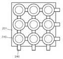
도 7은 상술한 광민감성 산화물 반도체를 갖는 광센서의 원리를 이용하여 구현된 리모트 터치 패널(200)의 예시적인 구조를 개략적으로 보이는 평면도이다. 도 7을 참조하면, 한 장의 광민감성 산화물 반도체층(201) 위로 행과 열 방향을 따라 다수의 전도성 라인(210, 220)들이 배열되어 있다. 예를 들어, 서로 평행한 다수의 행(row)을 이루는 수평 전도성 라인(210)들이 광민감성 산화물 반도체층(201) 위로 수평 방향을 따라 연장되어 있다. 또한, 상기 수평 전도성 라인(210)에 수직하게 배열되며, 서로 평행한 다수의 열(column)을 이루는 수직 전도성 라인(220)들이 광민감성 산화물 반도체층(201) 위로 수직 방향을 따라 연장되어 있다. 도면에서는 수평 전도성 라인(210)들과 수직 전도성 라인(220)들이 서로 접촉하여 교차하는 것으로 보이지만, 수평 전도성 라인(210)들과 수직 전도성 라인(220)들은 실제로는 서로 다른 높이에서 접촉하지 않고 교차한다. 이러한 수평 전도성 라인(210)들과 수직 전도성 라인(220)들은 투명 전극의 역할을 한다. 예를 들어, 상기 수평 및 수직 전도성 라인(210, 220)들은 ITO(Indium Tin Oxide)나 IZO(indium zinc oxide)와 같은 투명한 전도성 재료로 이루어질 수 있다.FIG. 7 is a plan view schematically showing an exemplary structure of a
또한, 상기 수평 및 수직 전도성 라인(210, 220)들은 광민감성 산화물 반도체층(201)과 직접적으로 접촉하지 않고, 전도성 컨택(215, 225)을 통해 광민감성 산화물 반도체층(201)과 전기적으로 연결될 수 있다. 예를 들어, 제 1 컨택(215)은 수평 전도성 라인(210)들과 광민감성 산화물 반도체층(201)을 전기적으로 연결시키도록 배치되며, 제 2 컨택(225)은 수직 전도성 라인(220)들과 광민감성 산화물 반도체층(201)들 전기적으로 연결시키도록 배치된다. 이를 위해, 제 1 컨택(215)의 일단은 광민감성 산화물 반도체층(201)과 접촉하고 타단은 수평 전도성 라인(210)과 접촉하여 있다. 제 2 컨택(225)의 일단은 광민감성 산화물 반도체층(201)과 접촉하고 타탄은 수직 전도성 라인(220)과 접촉하여 있다. 이러한 제 1 컨택(215)과 제 2 컨택(225)은 입사광의 위치를 감지하기 위한 하나의 광센서 셀(202)마다 각각 하나씩 배치될 수 있다. 또한, 도 7에 도시된 바와 같이, 상기 제 1 컨택(215)과 제 2 컨택(225)의 일부는 각각 수평 전도성 라인(210)과 수직 전도성 라인(220)으로부터 수직한 방향으로 광센서 셀(202)을 향해 연장되어 돌출될 수도 있다. 제 1 및 제 2 컨택(215, 225)도 역시 ITO나 IZO와 같은 투명한 전도성 재료로 이루어질 수 있다.In addition, the horizontal and vertical
이러한 구조에서, 다수의 수평 및 수직 전도성 라인(210, 220)들과 다수의 제 1 및 제 2 컨택(215, 225)들을 포함하는 다수의 광센서 셀(202)들이 한 장의 광민감성 산화물 반도체층(201)을 공유하고 있다. 그렇더라도, 광민감성 산화물 반도체층(201) 내에서 광이 입사하는 영역에서만 전류가 흐르고 광이 입사하지 않는 나머지 영역에서는 고저항 상태로 있기 때문에, 광이 입사하는 위치를 감지하는 데에는 문제가 없다. 예를 들어, 도 7을 참조하면, 광(L)이 입사하는 광센서 셀(202)에 전기적으로 연결된 제 1 컨택(215)과 제 2 컨택(225) 사이로만 전류가 흐르게 된다.In this structure, a plurality of
한편, 광센서 셀(202)들 사이의 구분을 더욱 명확히 하기 위하여, 광민감성 산화물 반도체층을 다수의 셀들로 패터닝하여 사용할 수도 있다. 도 8은 다수의 셀들로 패터닝된 광민감성 산화물 반도체층을 갖는 리모트 터치 패널(200')의 예시적인 구조를 개략적으로 보이는 평면도이다. 도 8을 참조하면, 리모트 터치 패널(200')은 다수의 분할된 광민감성 산화물 반도체 셀(201a), 행과 열 방향을 따라 배열된 다수의 수평 및 수직 전도성 라인(210, 220), 및 각각의 셀(201a)과 상기 수평 및 수직 전도성 라인(210, 220) 사이의 전기적 연결을 제공하는 다수의 제 1 및 제 2 컨택(215, 225)을 포함할 수 있다. 여기서, 각각의 광센서 셀(202)마다 광민감성 산화물 반도체 셀(201a)이 하나씩 배치될 수 있다. 도 7의 리모트 터치 패널(200)과 비교할 때, 도 8에 도시된 리모트 터치 패널(200')은, 하나의 광민감성 산화물 반도체층(201)이 다수의 광민감성 산화물 반도체 셀(201a)들로 분할되어 있다는 점에서만 차이가 있다. 나머지 수평 및 수직 전도성 라인(210, 220)과 제 1 및 제 2 컨택(215, 225)에 관한 내용은 도 7과 관련하여 설명한 것과 동일하다.Meanwhile, in order to further clarify the distinction between the
다만, 도 8의 예에서, 광민감성 산화물 반도체 셀(201a)들 사이에 간격이 존재하기 때문에, 도 9에 도시된 바와 같이, 그 간격을 통해 UV 광 또는 근청색광이 하부의 디스플레이 패널(111)에 입사할 수 있다. 이 경우, 에너지가 비교적 높은 UV 광 또는 근청색광이 디스플레이 패널(111)의 동작에 영향을 줄 수도 있다. 따라서, 도 8에 도시된 것과 같은 리모트 터치 패널(200')을 사용하는 경우에는, 하부의 디스플레이 패널(111)을 UV 광으로부터 보호하기 위한 보호층(예컨대, 블랙 매트릭스 또는 UV 필터 등)을 디스플레이 패널(111)의 표면에 또는 그 내부에 배치할 수도 있다.In the example of FIG. 8, since there is a gap between the photosensitive silicon
지금까지는 리모트 터치 패널(200, 200')이 디스플레이 장치(110)의 표면 위에 배치되는 경우만을 예로서 설명하였다. 그러나, 도 8의 예에서와 같이, 다수의 분할된 광민감성 산화물 반도체 셀(201a)들을 사용하는 경우에는, 리모터 터치 패널을 디스플레이 장치(110)의 디스플레이 패널(111) 내에 일체화시키는 것도 가능하다. 예를 들어, 디스플레이 패널(111) 내의 하나의 화소를 4개의 영역으로 분할하여, 3개의 영역은 각각 적, 녹, 청색을 위한 RGB 서브화소에 할당하고, 나머지 하나의 영역에 상술한 리모트 터치 패널(200')의 분할된 광민감성 산화물 반도체 셀(201a)을 포함하는 하나의 광센서 셀(202)을 배치할 수도 있다. 그러면, 디스플레이 장치와 리모트 터치 패널이 하나의 기판으로 일체화된 리모트 터치 스크린의 제공이 가능하다. 이 경우에도, 디스플레이 패널(111)을 UV 광으로부터 보호하기 위한 보호층을 디스플레이 패널(111)의 표면에 또는 그 내부에 배치할 수 있다.Up to now, only the cases where the
도 10은 상술한 수평 및 수직 전도성 라인(210, 220)들과 제 1 및 제 2 컨택(215, 225)들의 배치 구조 및 하나의 좌표로서 인식되는 광센서 셀(202)의 영역을 보다 자세하게 도시하고 있다. 도 10은 설명의 편의상 단지 두 개의 수평 전도성 라인(210a, 210b)들과 두 개의 수직 전도성 라인(220a, 220b)들만을 도시하고 있으며, 하부의 광민감성 산화물 반도체층(201)은 도시하지 않았다. 도 10을 참조하면, 제 1 및 제 2 수직 전도성 라인(220a, 220b) 위로 제 1 및 제 2 수평 전도성 라인(210a, 210b)이 지나고 있다. 각각의 수평 전도성 라인(210a, 210b) 아래에는 하부의 광민감성 산화물 반도체층(201)과의 전기적 연결을 위한 제 1 컨택(215)이 배치되며, 각각의 수직 전도성 라인(220a, 220b) 아래에도 광민감성 산화물 반도체층(201)과의 전기적 연결을 위한 제 2 컨택(225)이 배치된다.Figure 10 shows the arrangement of the horizontal and vertical
위와 같은 구조에서, 광민감성 산화물 반도체층(201)에 광이 입사하면 적어도 하나의 수평 전도성 라인(210a, 210b)과 적어도 하나의 수평 전도성 라인(220a, 220b) 사이에 전류가 흐르게 된다. 따라서, 어떠한 수평 전도성 라인(210a, 210b)과 수직 전도성 라인(220a, 220b) 사이에 전류가 흐르는 지를 감지하면, 광이 입사한 위치의 좌표를 구할 수 있다. 예컨대, 제 1 광(L1)이 광민감성 산화물 반도체층(201)에 입사하면 제 2 수평 전도성 라인(210b)과 제 2 수직 전도성 라인(220b) 사이로 전류가 흐르게 된다. 또한, 제 2 광(L2)이 광민감성 산화물 반도체층(201)에 입사하는 경우에도, 전류는 제 2 수평 전도성 라인(210b)과 제 2 수직 전도성 라인(220b) 사이로 흐르게 된다. 마찬가지로, 제 3 및 제 4 광(L3, L4)에 의해서도 전류는 제 2 수평 전도성 라인(210b)과 제 2 수직 전도성 라인(220b) 사이로 흐르게 된다. 따라서, 도 10에 예시적으로 도시된 네 개의 서로 다른 지점에 입사하는 광(L1~L4)의 좌표는 모두 동일하게 인식될 수 있다. 도 10에서 점선의 사각형으로 표시된 바와 같이, 이렇게 동일한 좌표로 인식될 수 있는 전체 영역을 하나의 광센서 셀(202)로 볼 수 있다.In this structure, when light is incident on the photosensitive
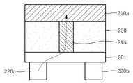
도 11은 도 10의 A-A' 라인에 대한 리모트 터치 패널(200, 200')의 단면의 한 예를 개략적으로 도시하고 있다. 도 11을 참조하면, 광민감성 산화물 반도체층(201) 위로 제 1 및 제 2 수직 전도성 라인(220a, 220b)과 제 1 수평 전도성 라인(210a)이 서로 떨어져서 배치되어 있다. 제 1 수평 전도성 라인(210a)과 광민감성 산화물 반도체층(201) 사이에는 제 1 컨택(215)이 연결되어 있다. 또한, 도 11에서 은선(hidden-line)으로 표시된 바와 같이, 광민감성 산화물 반도체층(201)과 제 1 및 제 2 수직 전도성 라인(220a, 220b) 사이에는 제 2 컨택(225)이 연결되어 있다. 도 10에서 알 수 있듯이, 제 2 컨택(225)은 제 1 수평 전도성 라인(210a)과 제 2 수평 전도성 라인(210b) 사이에 위치하기 때문에, 도 11의 단면도에서는 직접 보이지는 않는다. 그러나, 실시예에 따라서는 제 2 컨택(225)이 모든 수직 전도성 라인(220a, 220b)들 아래의 전체 영역을 따라 배치될 수도 있다. 이 경우에는, 제 2 컨택(225)도 도 11의 단면도에서 직접 보이게 된다. 한편, 광민감성 산화물 반도체층(201)의 표면 위에는 수평 및 수직 전도성 라인(210, 220)들을 덮도록 전체적으로 투명 절연층(230)이 채워질 수 있다. 투명 절연층(230)은 예를 들어 SiO2와 같은 재료로 이루어질 수 있다. 도 11에서 화살표는 광의 입사시에 형성되는 전류의 흐름 경로를 나타낸다.Fig. 11 schematically shows an example of a cross section of the
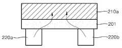
도 12 내지 도 14는 리모트 터치 패널(200, 200')의 다양한 다른 단면의 예를 개략적으로 도시하고 있다. 도 12를 참조하면, 제 2 컨택(225)을 생략하고 수직 전도성 라인(220a, 220b)들이 광민감성 산화물 반도체층(201) 위에 직접 접촉하여 배치될 수도 있다. 또한, 도 13을 참조하면, 수직 전도성 라인(220a, 220b)들이 광민감성 산화물 반도체층(201)의 반대쪽 표면 위에 직접 배치될 수도 있다. 여기서, 투명 절연층(230)은 수평 전도성 라인(210a)과 제 1 컨택(215)을 덮도록 광민감성 산화물 반도체층(201)의 표면 위에 채워진다. 더욱 간단하게는, 제 1 컨택(215)과 투명 절연층(230)을 더 생략하고, 광민감성 산화물 반도체층(201)의 한쪽 표면 위에 수평 전도성 라인(210a)이 직접 접촉하여 배치되며, 반대쪽 표면에 수직 전도성 라인(220a, 220b)이 직접 접촉하여 배치될 수도 있다. 도 12 내지 도 14에서 화살표는 광의 입사시에 형성되는 전류의 흐름 경로를 나타낸다. 도 11로부터 도 14로 갈수록 전류가 흐르는 경로가 점점 짧아진다는 것을 알 수 있다. 따라서 도 12 내지 도 14에 도시된 단면의 예는, 예를 들어 전류의 누설을 방지하기 위하여, UV 광 또는 근청색광이 조사되지 않은 상태에서는 상기 광민감성 산화물 반도체층(201)이 거의 완전한 절연체에 가까운 특성을 유지할 때 적용될 수 있다. 이 경우, 리모트 터치 패널(200, 200')의 구조가 간단해져서 제조 공정을 단순화할 수 있으며, 제조 비용을 저감시킬 수 있다.Figs. 12 to 14 schematically show various examples of different cross sections of the
한편, 상기 수평 및 수직 전도성 라인(210, 220)은 단순한 직선 라인의 형태뿐만 아니라 다양한 패턴의 형태를 가질 수도 있다. 도 15는 원형의 패턴(211)을 갖는 수평 전도성 라인(210)을 구비하는 리모트 터치 패널의 예가 개략적으로 도시하고 있다. 도 15를 참조하면, 수평 전도성 라인(210)은 일정한 간격으로 원형의 패턴(211)을 갖도록 형성되어 있다. 예를 들어, 수평 전도성 라인(210)은 리모트 터치 패널의 각각의 광센서 셀 영역마다 적어도 하나씩 원형 패턴(211)을 가질 수 있다. 이 경우, 원형 패턴(211)의 중심에 광이 입사할 때, 수평 전도성 라인(210)과 수직 전도성 라인(220) 사이로 전류가 흐르게 된다. 따라서, 광이 입사하는 위치의 좌표를 더욱 정확하게 특정하는 것이 가능하다.Meanwhile, the horizontal and vertical
또한, 도 15에는 원형의 패턴(211)이 도시되어 있으나, 상기 수평 전도성 라인(210)의 패턴은 원형이 아닌 타원형 또는 사각형과 같은 다각형 형태의 패턴일 수도 있다. 반면, 도 15에서 수직 전도성 라인(220)은 앞서 설명한 바와 같이 단순한 직선형으로 도시되어 있다. 그러나, 수평 전도성 라인(210) 대신에 수직 전도성 라인(220)이 원형이나 사각형과 같은 소정의 패턴을 가질 수도 있다. 또한, 수평 및 수직 전도성 라인(210, 220)이 모두 소정의 패턴을 갖는 것도 가능하다. 이 경우, 수평 전도성 라인(210)의 패턴과 수직 전도성 라인(220)의 패턴이 동일할 수도 있으며, 또는 상이할 수도 있다. 다만, 수평 및 수직 전도성 라인(210, 220)이 모두 소정의 패턴을 갖는 경우에, 수평 전도성 라인(210)의 패턴과 수직 전도성 라인(220)의 패턴의 위치가 정확하게 일치할 필요가 있다.Although a
도 16은 도 15에 도시된 리모트 터치 패널의 한 광센서 영역에 대한 단면도이다. 도 16을 참조하면, 광민감성 산화물 반도체층(201)의 상부 표면에 수평 전도성 라인(210)의 한 패턴(211)이 배치되어 있으며, 광민감성 산화물 반도체층(201)의 하부 표면에 수직 전도성 라인(220)이 배치되어 있다. 따라서, 도 16에 도시된 단면의 예는 도 14에 도시된 단면 구조를 적용한 것이다. 그러나, 도 12 및 도 13의 단면 구조에서도 수평 전도성 라인(210)이나 수직 전도성 라인(220)이 소정을 패턴을 갖는 것이 가능하다.16 is a cross-sectional view of the optical sensor area of the remote touch panel shown in Fig. 16, a
지금까지는, 리모트 터치 패널이 다수의 나란한 라인으로 구성된 수평 전도성 라인(210)과 수직 전도성 라인(220)을 전극으로서 갖는 경우에 대해 설명하였다. 그러나, 다른 형태의 전극 구조도 역시 가능하다. 도 17 및 도 18은 각각 소정의 패턴(245)을 갖는 상부 전극층(240)과 하나의 대면적 하부 전극층(250)을 구비하는 리모트 터치 패널의 예를 도시하는 평면도 및 단면도이다. 도 18의 단면도는, 도 16과 마찬가지로, 리모트 터치 패널의 한 광센서 영역에 대해서만 표시하고 있다. 도 17 및 도 18을 참조하면, 패턴이 없는 하나의 대면적 하부 전극층(250)이 광민감성 산화물 반도체층(201)의 하부 표면 전체 영역에 걸쳐 한 층으로 배치되어 있다. 또한, 광민감성 산화물 반도체층(201)의 상부 표면에는, 각각의 광센서 영역마다 적어도 하나의 원형의 패턴(245)을 갖는 상부 전극층(240)이 배치되어 있다. 앞서 설명한 바와 마찬가지로, 상기 상부 전극층(240)의 패턴은 원형이 아닌 타원형 또는 사각형과 같은 다각형 형태의 패턴일 수도 있다. 도 18에 도시된 바와 같이, 각각의 패턴(245)은 이웃하는 다른 패턴들과 모두 전기적으로 연결되어 있다. 따라서, 특정한 하나의 광센서 영역에서 발생한 광전류는 모든 패턴(245)들을 따라 상부 전극(240)의 전체로 흐르게 된다.Up to now, the case where the remote touch panel has the horizontal
도 19는 도 17 및 도 18에 도시된 리모트 터치 패널에서 광이 입사한 위치를 감지하는 원리를 설명한다. 도 19를 참조하면, 리모트 터치 패널의 어느 한 표면에 광(L)이 입사하면, 그 지점으로부터 광전류가 발생하여 상부 전극(240)을 따라 전체적으로 전류가 퍼지게 된다. 전류는 광(L)이 입사한 지점으로부터 멀어질수록 늦게 도달할 것이다. 따라서, 위치를 정확히 알고 있는 다수의 지점들 사이의 전류 도달 시간차를 측정하면, 광(L)이 입사한 지점을 계산하는 것이 가능하다. 예를 들어, 도 19에 도시된 바와 같이, 리모트 터치 패널의 네 꼭지점에 전류를 감지하는 센서(S1~S4)를 배치할 수 있다. 그러면, 네 개의 센서(S1~S4)에서 전류를 감지하는 순간의 시간들 사이의 차이를 측정할 수 있으며, 이러한 시간차를 기초로 리모트 터치 패널 상의 어느 위치에 광(L)이 입사하였는 지를 확인할 수 있다. 도 19에는 4개의 전류 감지 센서(S1~S4)가 광민감성 산화물 반도체층(201)의 네 꼭지점에 배치된 것으로 도시되어 있지만, 전류 감지 센서(S1~S4)의 위치가 반드시 그렇게 한정될 필요는 없다. 단지 위치를 정확히 알고 있는 다수의 지점들에 다수의 전류 감지 센서들이 위치하면 된다.FIG. 19 illustrates a principle of detecting the position of light incident on the remote touch panel shown in FIGS. 17 and 18. FIG. Referring to FIG. 19, when light L is incident on one surface of the remote touch panel, a photocurrent is generated from the point, and the current spreads along the
상술한 본 발명에 따른 리모트 터치 패널에서, 광이 입사하지 않는 동안의 전류의 누설을 더욱 줄이고 광이 입사할 때 전류가 더욱 용이하게 흐르도록 하기 위하여, 전극 재료의 일함수를 조절할 수 있다. 예를 들어, 수평 전도성 라인(210)과 수직 전도성 라인(220) 중에서 또는 상부 전극(240)과 하부 전극(250) 중에서 양의 전압이 인가되는 양극은 비교적 높은 일함수(workfunction)를 갖도록 처리될 수 있다. 예를 들어, 양극은 약 4.8~5.2eV 정도의 일함수를 갖도록 처리될 수 있다. 그러면, 양극은 전자 배리어(electron barrier)를 갖게 된다. 따라서, 광이 입사하지 않는 동안 광민감성 산화물 반도체층(201)과 양극 사이의 전자의 이동을 방지할 수 있다. 또한, 수평 전도성 라인(210)과 수직 전도성 라인(220) 중에서 또는 상부 전극(240)과 하부 전극(250) 중에서 음의 전압이 인가되거나 또는 그라운드에 연결되는 음극은 비교적 낮은 일함수를 갖도록 처리될 수 있다. 예를 들어, 음극은 약 4.1~4.5eV 정도의 일함수를 갖도록 처리될 수 있다. 그러면, 음극은 정공 배리어(hole barrier)를 갖게 된다. 따라서, 광이 입사하지 않는 동안 광민감성 산화물 반도체층(201)과 음극 사이의 정공의 이동을 방지할 수 있다. 이러한 양극과 음극의 일함수는 예를 들어, ITO나 IZO를 재료로 사용하는 경우에, 인듐과 주석 사이의 성분비 또는 인듐과 아연 사이의 성분비를 조절함으로써 달성될 수 있다.In the remote touch panel according to the present invention, the work function of the electrode material can be adjusted in order to further reduce the leakage of current while the light is not incident and allow the current to flow more easily when the light is incident. For example, one of the horizontal
지금까지 광센서를 이용한 리모트 터치 패널의 다양한 가능한 구조에 대하여 논의하였다. 이러한 리모트 터치 패널에서, 리모트 터치 패널에 입사하는 UV 광 또는 근청색광 신호를 다양하게 변화시킴으로써 리모트 터치 패널이 다양한 기능을 수행하도록 할 수 있다.Various possible structures of remote touch panel using optical sensor have been discussed. In such a remote touch panel, the remote touch panel can perform various functions by variously changing the UV light or the near-ultraviolet light signal incident on the remote touch panel.
도 20a 내지 도 20i는 리모트 터치 패널에 입사할 수 있는 다양한 광신호의 예를 보이고 있다. 예를 들어, 도 20a은 원형의 광신호가 그 중심을 유지한 채 전 방향으로 비례적으로 크기를 확장하는 예를 보이고 있다. 이하의 도면에서 화살표는 광신호가 확장되는 방향을 표시한다. 또한, 도 20b는 원형의 광신호가 수평 방향으로 확장되면서 타원형으로 되는 예를 보이고 있다. 또한, 도 20c와 도 20d는 원형의 광신호가 대각선 방향으로 확장되는 예를 보이고 있으며, 도 20e는 원형의 광신호가 수직 방향으로 확장되는 예를 보이고 있다. 또한, 도 20f는 원형의 광신호가 대각선 방향으로 중심을 이동하면서 확장되는 예를 보이고 있다. 도 20g와 도 30h는 원형이 아닌 별모양 및 십자가 모양의 광신호의 예를 보이고 있다. 또한 도 20i는 광신호가 펄스와 같이 일정한 시간 간격으로 연속하여 입사되는 예를 보이고 있다. 이때, 소정의 시간 주기 내에서 광신호의 연속적인 입사 횟수를 변화시킬 수 있다. 도시하지는 않았지만, 예를 들어, 광신호가 입사하는 시간의 변화, 입사하는 광신호의 광량의 변화, 입사하는 광신호의 파장의 변화와 같은 다른 광신호의 변화들도 이용이 가능하다.20A to 20I show examples of various optical signals that can be incident on the remote touch panel. For example, FIG. 20A shows an example in which a circular optical signal extends in a proportional manner in all directions while maintaining its center. In the following drawings, the arrow indicates the direction in which the optical signal extends. 20B shows an example in which a circular optical signal is extended in the horizontal direction to an elliptical shape. 20C and 20D show an example in which a circular optical signal is extended in a diagonal direction, and FIG. 20E shows an example in which a circular optical signal is extended in a vertical direction. In addition, FIG. 20F shows an example in which a circular optical signal is expanded while moving in the diagonal direction. FIGS. 20G and 30H show examples of a star-shaped and cross-shaped optical signal instead of a circular shape. FIG. 20I shows an example in which the optical signal is continuously incident at a constant time interval like a pulse. At this time, it is possible to change the number of successive incidence of the optical signal within a predetermined time period. Although not shown, other optical signal variations such as a change in the time at which the optical signal is incident, a change in the amount of the incident optical signal, and a change in the wavelength of the incident optical signal are also available.
이러한 광신호의 변화에 따라, 예를 들어 디스플레이 장치에서 디스플레이 되는 영상의 일부 또는 전체의 이동, 확대, 축소, 숨김, 회전과 같은 동작을 수행할 수 있다. 또한, 디스플레이 장치나 컴퓨터 시스템, TV 등에서의 특정 메뉴의 선택, 실행, 취소와 같은 동작을 수행할 수도 있다. 특히, 3D 디스플레이 장치를 사용하는 경우에, 3D 디스플레이 장치에서 디스플레이 되는 영상의 깊이 조절 명령이 가능할 수도 있다. 예를 들어, 도 20a 또는 도 20f와 같은 광신호의 확대시에 광신호가 입사하는 영역에 있는 특정 영상이 더 가까이 보이게(즉, 깊이가 얕게) 할 수 있으며, 또는 광신호의 축소시에 광신호가 입사하는 영역에 있는 특정 영상이 더 멀리 보이게(즉, 깊이가 깊게) 할 수 있다. 이러한 방식으로 사용자는 레이저 포인터와 같은 간단한 광원 장치를 이용하여 복잡하고 다양한 동작을 원격으로 제어할 수 있다.Depending on the change of the optical signal, for example, it is possible to perform operations such as movement, enlargement, reduction, hiding, and rotation of part or all of the image displayed on the display device. It is also possible to perform operations such as selection, execution and cancellation of a specific menu in a display device, a computer system, a TV, and the like. In particular, in the case of using a 3D display device, it may be possible to instruct the 3D display device to adjust the depth of the displayed image. For example, when enlarging an optical signal as shown in Fig. 20A or Fig. 20F, a specific image in an area where an optical signal enters may be made closer (i.e., the depth is shallower), or when the optical signal is reduced A particular image in the incident area can be seen to be farther away (i.e., deep in depth). In this way, the user can remotely control complex and various operations using a simple light source device such as a laser pointer.
지금까지, 본 발명의 이해를 돕기 위하여 광센서를 이용한 리모트 터치 패널 및 이를 구비하는 리모트 터치 스크린 장치에 대한 예시적인 실시예가 설명되고 첨부된 도면에 도시되었다. 그러나, 이러한 실시예는 단지 본 발명을 예시하기 위한 것이고 이를 제한하지 않는다는 점이 이해되어야 할 것이다. 그리고 본 발명은 도시되고 설명된 설명에 국한되지 않는다는 점이 이해되어야 할 것이다. 이는 다양한 다른 변형이 본 기술분야에서 통상의 지식을 가진 자에게 일어날 수 있기 때문이다.Up to now, an exemplary embodiment of a remote touch panel using a photosensor and a remote touch screen device having the same has been described and shown in the accompanying drawings to facilitate understanding of the present invention. It should be understood, however, that such embodiments are merely illustrative of the present invention and not limiting thereof. And it is to be understood that the invention is not limited to the details shown and described. Since various other modifications may occur to those of ordinary skill in the art.
10.....광센서11.....광민감성 반도체
12.....제 1 전극13.....제 2 전극
100....리모트 터치 스크린 장치110....디스플레이 장치
111....디스플레이 패널115....백라이트 유닛
120....광원 장치200....리모트 터치 패널
201....광민감성 산화물 반도체층202....광센서 셀
210....수평 전도성 라인215....제 1 컨택
220....수직 전도성 라인225....제 2 컨택
230....투명 절연층240....상부 전극층
250....하부 전극층10 .....
12 .....
100 .... Remote
111 ....
120 ....
201 ... light-sensitive
210 .... horizontal
220 .... vertical
230 .... transparent insulating
250 .... Lower electrode layer
Claims (25)
Translated fromKorean각각의 광센서 셀은 광민감성 반도체층; 및
상기 광민감성 반도체층과 전기적으로 연결된 제 1 전극 및 제 2 전극을 포함하고,
상기 광민감성 반도체층은 빛이 조사에 의해 전자와 정공을 생성하여 광전류를 발생시키는 광민감성 산화물 반도체 재료로 이루어지며,
상기 제 1 전극과 제 2 전극은 서로 접촉하지 않도록 배치된 리모트 터치 패널.A plurality of optical sensor cells arranged two-dimensionally,
Each photosensor cell comprises a light-sensitive semiconductor layer; And
A first electrode and a second electrode electrically connected to the light-sensitive semiconductor layer,
The light-sensitive semiconductor layer is made of a light-sensitive oxide semiconductor material that generates electrons and holes by light irradiation to generate a photocurrent,
Wherein the first electrode and the second electrode are disposed so as not to contact each other.
상기 광민감성 산화물 반도체 재료는 가시광선을 통과시키며 400nm 이하의 파장을 갖는 광을 흡수하여 전자와 홀을 생성시키는 리모트 터치 패널.The method according to claim 1,
Wherein the light-sensitive oxide semiconductor material transmits visible light and absorbs light having a wavelength of 400 nm or less to generate electrons and holes.
상기 광민감성 산화물 반도체 재료는 ZnOx, doped-ZnOx 또는 InZnO인 리모트 터치 패널.The method according to claim 1,
Wherein the photo-sensitive oxide semiconductor material is ZnOx , doped-ZnOx, or InZnO.
상기 광민감성 반도체층은 각각의 광센서 셀마다 하나씩 배치된 다수의 광민감성 반도체 셀들로 분할되어 있으며,
다수의 평행한 제 1 전극들이 상기 다수의 광민감성 반도체 셀들에 걸쳐 제 1 방향을 따라 연장되어 있고, 다수의 평행한 제 2 전극들이 상기 다수의 광민감성 반도체 셀들에 걸쳐 상기 제 1 방향과 수직한 제 2 방향을 따라 연장되어 있는 리모트 터치 패널.The method according to claim 1,
The light-sensitive semiconductor layer is divided into a plurality of light-sensitive semiconductor cells, one for each optical sensor cell,
A plurality of parallel first electrodes extending along a first direction across the plurality of photo sensitive semiconductor cells and a plurality of parallel second electrodes extending perpendicular to the first direction across the plurality of photo sensitive semiconductor cells And extending along a second direction.
상기 제 1 전극과 광민감성 반도체층을 전기적으로 연결시키도록 배치된 제 1 컨택; 및
상기 제 2 전극과 광민감성 반도체층을 전기적으로 연결시키도록 배치된 제 2 컨택을 더 포함하며,
상기 제 1 컨택과 제 2 컨택은 각각의 광센서 셀마다 하나씩 배치되는 리모트 터치 패널.6. The method of claim 5,
A first contact arranged to electrically connect the first electrode and the photosensitive semiconductor layer; And
Further comprising a second contact arranged to electrically connect the second electrode and the light-sensitive semiconductor layer,
Wherein the first contact and the second contact are disposed one by one for each optical sensor cell.
상기 제 1 컨택의 일부와 제 2 컨택의 일부가 각각 제 1 전극과 제 2 전극으로부터 수직한 방향으로 연장되어 돌출되어 있는 리모트 터치 패널.The method according to claim 6,
Wherein a part of the first contact and a part of the second contact each protrude from the first electrode and the second electrode in a vertical direction.
다수의 광센서 셀들이 한 장의 광민감성 반도체층을 공유하며,
다수의 평행한 제 1 전극들이 상기 광민감성 반도체층에 걸쳐 제 1 방향을 따라 연장되어 있고, 다수의 평행한 제 2 전극들이 상기 광민감성 반도체층에 걸쳐 상기 제 1 방향과 수직한 제 2 방향을 따라 연장되어 있는 리모트 터치 패널.The method according to claim 1,
A plurality of optical sensor cells share a single photosensitive semiconductor layer,
A plurality of parallel first electrodes extending along a first direction across the photosensitive semiconductor layer and a plurality of parallel second electrodes extending in a second direction perpendicular to the first direction across the photosensitive semiconductor layer The extended remote touch panel.
상기 제 1 전극과 광민감성 반도체층을 전기적으로 연결시키도록 배치된 제 1 컨택; 및
상기 제 2 전극과 광민감성 반도체층을 전기적으로 연결시키도록 배치된 제 2 컨택을 더 포함하며,
상기 제 1 컨택과 제 2 컨택은 각각의 광센서 셀마다 하나씩 배치되는 리모트 터치 패널.9. The method of claim 8,
A first contact arranged to electrically connect the first electrode and the photosensitive semiconductor layer; And
Further comprising a second contact arranged to electrically connect the second electrode and the light-sensitive semiconductor layer,
Wherein the first contact and the second contact are disposed one by one for each optical sensor cell.
상기 제 1 컨택의 일부와 제 2 컨택의 일부가 각각 제 1 전극과 제 2 전극으로부터 수직한 방향으로 연장되어 돌출되어 있는 리모트 터치 패널.10. The method of claim 9,
Wherein a part of the first contact and a part of the second contact each protrude from the first electrode and the second electrode in a vertical direction.
상기 제 1 및 제 2 전극들을 덮도록 상기 광민감성 반도체층의 표면 위에 전체적으로 채워져 있는 투명 절연층을 더 포함하며,
상기 제 1 전극과 제 2 전극은 광민감성 반도체층의 동일한 표면 위로 서로 접촉하지 않고 교차하는 리모트 터치 패널.10. The method of claim 9,
And a transparent insulation layer that is entirely filled on the surface of the photosensitive semiconductor layer to cover the first and second electrodes,
Wherein the first electrode and the second electrode cross over the same surface of the photosensitive semiconductor layer without contacting each other.
상기 제 1 전극과 광민감성 반도체층을 전기적으로 연결시키도록 배치된 제 1 컨택; 및
상기 제 1 및 제 2 전극들을 덮도록 상기 광민감성 반도체층의 표면 위에 전체적으로 채워져 있는 투명 절연층을 더 포함하며,
상기 제 2 전극은 상기 광민감성 반도체층의 표면 위에 직접 접촉하여 배치되고,
상기 제 1 전극과 제 2 전극은 광민감성 반도체층의 동일한 표면 위로 서로 접촉하지 않고 교차하는 리모트 터치 패널.9. The method of claim 8,
A first contact arranged to electrically connect the first electrode and the photosensitive semiconductor layer; And
And a transparent insulation layer that is entirely filled on the surface of the photosensitive semiconductor layer to cover the first and second electrodes,
The second electrode is disposed in direct contact with the surface of the photosensitive semiconductor layer,
Wherein the first electrode and the second electrode cross over the same surface of the photosensitive semiconductor layer without contacting each other.
상기 제 1 전극과 광민감성 반도체층을 전기적으로 연결시키도록 배치된 제 1 컨택; 및
상기 제 1 전극 및 제 1 컨택을 덮도록 상기 광민감성 반도체층의 한 표면 위에 전체적으로 채워져 있는 투명 절연층을 더 포함하며,
상기 제 2 전극은 상기 광민감성 반도체층의 반대쪽 표면 위에 직접 접촉하여 배치되는 리모트 터치 패널.9. The method of claim 8,
A first contact arranged to electrically connect the first electrode and the photosensitive semiconductor layer; And
Further comprising a transparent insulation layer that is entirely filled on one surface of the photosensitive semiconductor layer to cover the first electrode and the first contact,
Wherein the second electrode is disposed in direct contact with the opposite surface of the light-sensitive semiconductor layer.
상기 제 1 전극은 상기 광민감성 반도체층의 한 표면 위에 직접 접촉하여 배치되며, 상기 제 2 전극은 상기 광민감성 반도체층의 반대쪽 표면 위에 직접 접촉하여 배치되는 리모트 터치 패널.9. The method of claim 8,
Wherein the first electrode is disposed in direct contact with one surface of the photosensitive semiconductor layer and the second electrode is disposed in direct contact with the opposite surface of the photosensitive semiconductor layer.
상기 제 1 전극과 제 2 전극 중 적어도 하나는 각각의 광센서 셀 영역마다 적어도 하나씩 원형, 타원형 또는 다각형 형태의 패턴을 갖는 리모트 터치 패널.9. The method of claim 8,
Wherein at least one of the first electrode and the second electrode has at least one circular, elliptical or polygonal pattern for each optical sensor cell region.
다수의 광센서 셀들이 한 장의 광민감성 반도체층을 공유하며,
상기 제 1 전극은 각각의 광센서 셀 영역마다 적어도 하나의 원형, 타원형 또는 다각형 형태의 패턴을 갖도록 상기 광민감성 반도체층의 한 표면 위에 배치되고,
상기 제 2 전극은 상기 광민감성 반도체층의 반대쪽 표면 전체 영역에 걸쳐서 패턴이 없이 한 층으로 배치되어 있는 리모트 터치 패널.The method according to claim 1,
A plurality of optical sensor cells share a single photosensitive semiconductor layer,
Wherein the first electrode is disposed on one surface of the photosensitive semiconductor layer so as to have at least one circular, elliptical or polygonal pattern for each photosensor cell region,
Wherein the second electrode is disposed as a single layer over the entire area of the surface opposite to the light-sensitive semiconductor layer without a pattern.
상기 광민감성 반도체층 상의 정확히 설정된 지점들에 각각 배치된 다수의 전류 감지 센서들을 더 포함하는 리모트 터치 패널.17. The method of claim 16,
Further comprising a plurality of current sensing sensors respectively disposed at precisely set points on the photosensitive semiconductor layer.
상기 제 1 및 제 2 전극은 투명 전극인 리모트 터치 패널.The method according to claim 1,
Wherein the first and second electrodes are transparent electrodes.
상기 투명 전극은 ITO 또는 IZO로 이루어지는 리모트 터치 패널.19. The method of claim 18,
Wherein the transparent electrode is made of ITO or IZO.
상기 제 1 전극과 제 2 전극 중에서 양의 전압이 인가되는 양극은 상대적으로 높은 일함수를 갖도록 처리되며, 음극은 상대적으로 낮은 일함수를 갖도록 처리되는 리모트 터치 패널.The method according to claim 1,
Wherein the positive electrode of the first electrode and the positive electrode of the second electrode are processed to have a relatively high work function and the negative electrode is processed to have a relatively low work function.
상대적으로 높은 일함수를 갖는 양극은 4.8~5.2eV의 일함수를 가지며, 상대적으로 낮은 일함수를 갖는 음극은 4.1~4.5eV의 일함수를 갖는 리모트 터치 패널.The method according to claim 1,
The anode having a relatively high work function has a work function of 4.8 to 5.2 eV and the cathode having a relatively low work function has a work function of 4.1 to 4.5 eV.
영상을 디스플레이 하는 디스플레이 장치; 및
상기 리모트 터치 패널에 조사되는 광신호를 제공하는 광원 장치;를 포함하는 리모트 터치 스크린 장치.A remote touch panel according to any one of claims 1 and 3 to 21,
A display device for displaying an image; And
And a light source device for providing an optical signal irradiated to the remote touch panel.
상기 디스플레이 장치에서 하나의 화소가 4개의 영역으로 분할되어 있으며, 상기 4개의 영역 중에서 3개의 영역은 각각 적, 녹, 청색을 위한 RGB 서브화소에 할당되고, 나머지 하나의 영역에는 상기 리모트 터치 패널의 하나의 광센서 셀이 배치되어 있는 리모트 터치 스크린 장치.23. The method of claim 22,
In the display device, one pixel is divided into four regions, and three of the four regions are allocated to red, green, and blue RGB sub-pixels, A remote touch screen device in which one optical sensor cell is disposed.
상기 리모트 터치 패널에 조사되는 광신호의 변화에 따라, 상기 디스플레이 장치에서 디스플레이 되는 영상의 일부 또는 전체에 대한 이동, 확대, 축소, 숨김, 회전 동작이 수행되거나 특정 메뉴의 선택, 실행, 취소 동작이 수행되는 리모트 터치 스크린 장치.23. The method of claim 22,
Enlargement, reduction, hiding, and rotation of a part or all of an image displayed on the display device in response to a change in an optical signal irradiated to the remote touch panel or performing a selection, execution, or cancellation of a specific menu A remote touch-screen device being performed.
상기 광신호의 변화는, 광신호의 크기의 비례적인 확대 또는 축소, 광신호의 이동, 어느 한 방향만으로의 광신호의 확장, 광신호의 모양 변화, 광신호가 입사하는 시간의 변화, 광신호의 광량의 변화, 광신호의 파장의 변화, 소정의 시간 주기 내에서 광신호의 연속적인 입사 횟수의 변화 중에서 어느 하나 또는 이들의 조합을 포함하는 리모트 터치 스크린 장치.25. The method of claim 24,
The change of the optical signal may include a proportional increase or decrease in the magnitude of the optical signal, a movement of the optical signal, an expansion of the optical signal in only one direction, a change in the shape of the optical signal, A change in the amount of light, a change in the wavelength of the optical signal, and a change in the number of continuous incidence of the optical signal within a predetermined time period, or a combination thereof.
Priority Applications (2)
| Application Number | Priority Date | Filing Date | Title |
|---|---|---|---|
| KR1020100030509AKR101643376B1 (en) | 2010-04-02 | 2010-04-02 | Remote touch panel using light sensor and remote touch screen apparatus having the same |
| US12/923,243US9092081B2 (en) | 2010-04-02 | 2010-09-10 | Remote touch panel using light sensor and remote touch screen apparatus having the same |
Applications Claiming Priority (1)
| Application Number | Priority Date | Filing Date | Title |
|---|---|---|---|
| KR1020100030509AKR101643376B1 (en) | 2010-04-02 | 2010-04-02 | Remote touch panel using light sensor and remote touch screen apparatus having the same |
Publications (2)
| Publication Number | Publication Date |
|---|---|
| KR20110111110A KR20110111110A (en) | 2011-10-10 |
| KR101643376B1true KR101643376B1 (en) | 2016-07-28 |
Family
ID=44709029
Family Applications (1)
| Application Number | Title | Priority Date | Filing Date |
|---|---|---|---|
| KR1020100030509AActiveKR101643376B1 (en) | 2010-04-02 | 2010-04-02 | Remote touch panel using light sensor and remote touch screen apparatus having the same |
Country Status (2)
| Country | Link |
|---|---|
| US (1) | US9092081B2 (en) |
| KR (1) | KR101643376B1 (en) |
Families Citing this family (19)
| Publication number | Priority date | Publication date | Assignee | Title |
|---|---|---|---|---|
| CN102759998A (en)* | 2011-04-25 | 2012-10-31 | 鸿富锦精密工业(深圳)有限公司 | Peripheral type touch control keyboard |
| KR101810608B1 (en) | 2011-06-22 | 2017-12-21 | 삼성전자주식회사 | Light sensing apparatus and method of driving the light sensing apparatus, and optical touch screen apparatus including the light sensing apparatus |
| KR101909676B1 (en) | 2012-05-25 | 2018-10-19 | 삼성디스플레이 주식회사 | Display device and optical inputting device |
| WO2014021479A1 (en)* | 2012-07-30 | 2014-02-06 | 서울시립대학교 산학협력단 | Display device capable of optical pointing input |
| KR101984737B1 (en) | 2012-09-21 | 2019-06-03 | 삼성디스플레이 주식회사 | Touch system comprising optical touch panel and touch pen, and method of controlling interference optical signal in touch system |
| TWM448018U (en)* | 2012-10-31 | 2013-03-01 | Nuvoton Technology Corp | Touch sensing panel |
| CN103854595A (en)* | 2012-11-29 | 2014-06-11 | 鸿富锦精密工业(深圳)有限公司 | Writing apparatus, light emitting diode display panel, and emitter |
| KR101856795B1 (en)* | 2013-09-11 | 2018-05-10 | 동우 화인켐 주식회사 | Laser Pointing Display Device |
| KR20160008843A (en)* | 2014-07-15 | 2016-01-25 | 삼성전자주식회사 | Display apparatus and control method thereof |
| US9507162B1 (en)* | 2014-09-19 | 2016-11-29 | Amazon Technologies, Inc. | Display component assembly |
| ES2600310B1 (en)* | 2015-08-07 | 2017-09-08 | Miguel SANZ FERNÁNDEZ | System and procedure for mouse emulation by light beam |
| CN105117075B (en)* | 2015-09-24 | 2018-03-09 | 京东方科技集团股份有限公司 | A kind of smooth touch base plate, In-cell touch panel and display device |
| KR101969831B1 (en)* | 2017-08-28 | 2019-04-17 | 주식회사 하이딥 | Touch sensor panel |
| CN109426388B (en)* | 2017-09-01 | 2021-05-25 | 京东方科技集团股份有限公司 | Display substrate, display device and control method thereof |
| CN109725751A (en)* | 2017-10-27 | 2019-05-07 | 深圳欧菲光科技股份有限公司 | Touch screen, display device and manufacturing method of touch screen |
| KR20190054359A (en) | 2017-11-13 | 2019-05-22 | 동우 화인켐 주식회사 | Input Sensor and Display Device Including the Same |
| CN111474735B (en)* | 2020-04-29 | 2022-08-23 | 深圳市华星光电半导体显示技术有限公司 | Light beam emitter and display device |
| CN112947787B (en)* | 2021-02-23 | 2024-09-06 | 北京京东方显示技术有限公司 | Touch panel, display device, display system and touch method |
| CN115202517A (en)* | 2022-06-30 | 2022-10-18 | 昆山国显光电有限公司 | A touch device and touch method |
Citations (2)
| Publication number | Priority date | Publication date | Assignee | Title |
|---|---|---|---|---|
| WO2002049367A2 (en)* | 2000-12-14 | 2002-06-20 | 3Dv Systems, Ltd. | Improved photosurface for a 3d camera |
| JP2007526448A (en)* | 2003-06-17 | 2007-09-13 | カネスタ インコーポレイテッド | Method and apparatus for charge management in three-dimensional and color detection |
Family Cites Families (16)
| Publication number | Priority date | Publication date | Assignee | Title |
|---|---|---|---|---|
| US5926168A (en)* | 1994-09-30 | 1999-07-20 | Fan; Nong-Qiang | Remote pointers for interactive televisions |
| JPH10289053A (en) | 1997-04-15 | 1998-10-27 | Matsushita Electric Ind Co Ltd | Coordinate position detector |
| US6566685B2 (en)* | 2000-04-12 | 2003-05-20 | Casio Computer Co., Ltd. | Double gate photo sensor array |
| US7663606B2 (en)* | 2004-03-19 | 2010-02-16 | Igt | Apparatus and method for configuring a touch screen |
| JP2006011569A (en) | 2004-06-23 | 2006-01-12 | Citizen Seimitsu Co Ltd | Optical touch panel |
| JP4556700B2 (en) | 2005-02-17 | 2010-10-06 | カシオ計算機株式会社 | Coordinate detection device |
| GB2437768A (en)* | 2006-05-03 | 2007-11-07 | Seiko Epson Corp | Photosensing TFT |
| US7898042B2 (en)* | 2006-11-07 | 2011-03-01 | Cbrite Inc. | Two-terminal switching devices and their methods of fabrication |
| CN101211246B (en)* | 2006-12-26 | 2010-06-23 | 乐金显示有限公司 | organic light emitting diode panel and touch screen system including the same |
| US20080303037A1 (en)* | 2007-06-04 | 2008-12-11 | Irving Lyn M | Methods of making thin film transistors comprising zinc-oxide-based semiconductor materials and transistors made thereby |
| JP4506785B2 (en)* | 2007-06-14 | 2010-07-21 | エプソンイメージングデバイス株式会社 | Capacitive input device |
| US7940252B2 (en)* | 2007-10-18 | 2011-05-10 | Himax Technologies Limited | Optical sensor with photo TFT |
| KR20090077350A (en) | 2008-01-11 | 2009-07-15 | 정병주 | Transparent film and input device coated with transparent position pattern in specific wavelength band and its use |
| JP5138529B2 (en)* | 2008-10-03 | 2013-02-06 | 株式会社ジャパンディスプレイイースト | Touch panel |
| US20100245370A1 (en)* | 2009-03-25 | 2010-09-30 | Qualcomm Mems Technologies, Inc. | Em shielding for display devices |
| TWI394071B (en)* | 2009-08-14 | 2013-04-21 | Au Optronics Corp | Oled touch panel and method of forming the same |
- 2010
- 2010-04-02KRKR1020100030509Apatent/KR101643376B1/enactiveActive
- 2010-09-10USUS12/923,243patent/US9092081B2/enactiveActive
Patent Citations (2)
| Publication number | Priority date | Publication date | Assignee | Title |
|---|---|---|---|---|
| WO2002049367A2 (en)* | 2000-12-14 | 2002-06-20 | 3Dv Systems, Ltd. | Improved photosurface for a 3d camera |
| JP2007526448A (en)* | 2003-06-17 | 2007-09-13 | カネスタ インコーポレイテッド | Method and apparatus for charge management in three-dimensional and color detection |
Also Published As
| Publication number | Publication date |
|---|---|
| US20110241989A1 (en) | 2011-10-06 |
| US9092081B2 (en) | 2015-07-28 |
| KR20110111110A (en) | 2011-10-10 |
Similar Documents
| Publication | Publication Date | Title |
|---|---|---|
| KR101643376B1 (en) | Remote touch panel using light sensor and remote touch screen apparatus having the same | |
| CN113424325B (en) | Touch display panel and electronic device | |
| CN112567322B (en) | Display device | |
| US10452201B1 (en) | Touch sensor for display with shield | |
| KR101929427B1 (en) | Display device including touch sensor | |
| KR102562627B1 (en) | Display device | |
| CN107425041A (en) | Touch display panel, device and manufacturing method | |
| KR101611418B1 (en) | Optical touch panel and method of fabricating the same | |
| KR101631984B1 (en) | Light sensing circuit, method of fabricating the light sensing circuit, and optical touch panel including the light sensing circuit | |
| CN102043272B (en) | Liquid crystal display device | |
| US20230049317A1 (en) | Touch substrate and display panel | |
| WO2018099176A1 (en) | Display substrate and manufacturing method therefor, fingerprint recognition apparatus, and display apparatus | |
| US11003287B2 (en) | Touch sensor for display with improved viewing angle uniformity | |
| JP2008096523A (en) | Display device | |
| TWI395008B (en) | Touch panel and touch display device | |
| WO2016165551A1 (en) | Oled display substrate, touch display panel and display device | |
| TWI460639B (en) | System for display images | |
| KR20130037072A (en) | Optical touch screen apparatus and method of fabricating the optical touch screen apparatus | |
| KR101899482B1 (en) | Light sensing circuit, method of fabricating the light sensing circuit, and optical touch panel including the light sensing circuit | |
| KR20120035744A (en) | Touch screen panel of electric capacity type having via hole and method of manufacturing the same | |
| CN101819494B (en) | Image display system | |
| CN101882022A (en) | sensory display panel | |
| CN114096939B (en) | Touch structure, touch display panel and electronic device | |
| US10719154B2 (en) | Display substrate and fabrication method thereof, display panel and display system | |
| CN102043538A (en) | Light-induced touch screen and detection system thereof |
Legal Events
| Date | Code | Title | Description |
|---|---|---|---|
| PA0109 | Patent application | Patent event code:PA01091R01D Comment text:Patent Application Patent event date:20100402 | |
| PG1501 | Laying open of application | ||
| A201 | Request for examination | ||
| PA0201 | Request for examination | Patent event code:PA02012R01D Patent event date:20150311 Comment text:Request for Examination of Application Patent event code:PA02011R01I Patent event date:20100402 Comment text:Patent Application | |
| E902 | Notification of reason for refusal | ||
| PE0902 | Notice of grounds for rejection | Comment text:Notification of reason for refusal Patent event date:20151019 Patent event code:PE09021S01D | |
| E701 | Decision to grant or registration of patent right | ||
| PE0701 | Decision of registration | Patent event code:PE07011S01D Comment text:Decision to Grant Registration Patent event date:20160421 | |
| GRNT | Written decision to grant | ||
| PR0701 | Registration of establishment | Comment text:Registration of Establishment Patent event date:20160721 Patent event code:PR07011E01D | |
| PR1002 | Payment of registration fee | Payment date:20160722 End annual number:3 Start annual number:1 | |
| PG1601 | Publication of registration | ||
| PR1001 | Payment of annual fee | Payment date:20200618 Start annual number:5 End annual number:5 | |
| PR1001 | Payment of annual fee | Payment date:20210617 Start annual number:6 End annual number:6 | |
| PR1001 | Payment of annual fee | Payment date:20230620 Start annual number:8 End annual number:8 | |
| PR1001 | Payment of annual fee | Payment date:20250612 Start annual number:10 End annual number:10 |