KR101641860B1 - Light-emitting element array, Backlight apparatus, and Illumination apparatus - Google Patents
Light-emitting element array, Backlight apparatus, and Illumination apparatusDownload PDFInfo
- Publication number
- KR101641860B1 KR101641860B1KR1020100044602AKR20100044602AKR101641860B1KR 101641860 B1KR101641860 B1KR 101641860B1KR 1020100044602 AKR1020100044602 AKR 1020100044602AKR 20100044602 AKR20100044602 AKR 20100044602AKR 101641860 B1KR101641860 B1KR 101641860B1
- Authority
- KR
- South Korea
- Prior art keywords
- light emitting
- circuit board
- printed circuit
- light
- emitting element
- Prior art date
- Legal status (The legal status is an assumption and is not a legal conclusion. Google has not performed a legal analysis and makes no representation as to the accuracy of the status listed.)
- Expired - Fee Related
Links
Images


Classifications
- F—MECHANICAL ENGINEERING; LIGHTING; HEATING; WEAPONS; BLASTING
- F21—LIGHTING
- F21K—NON-ELECTRIC LIGHT SOURCES USING LUMINESCENCE; LIGHT SOURCES USING ELECTROCHEMILUMINESCENCE; LIGHT SOURCES USING CHARGES OF COMBUSTIBLE MATERIAL; LIGHT SOURCES USING SEMICONDUCTOR DEVICES AS LIGHT-GENERATING ELEMENTS; LIGHT SOURCES NOT OTHERWISE PROVIDED FOR
- F21K9/00—Light sources using semiconductor devices as light-generating elements, e.g. using light-emitting diodes [LED] or lasers
- F21K9/20—Light sources comprising attachment means
- F21K9/27—Retrofit light sources for lighting devices with two fittings for each light source, e.g. for substitution of fluorescent tubes
- F—MECHANICAL ENGINEERING; LIGHTING; HEATING; WEAPONS; BLASTING
- F21—LIGHTING
- F21V—FUNCTIONAL FEATURES OR DETAILS OF LIGHTING DEVICES OR SYSTEMS THEREOF; STRUCTURAL COMBINATIONS OF LIGHTING DEVICES WITH OTHER ARTICLES, NOT OTHERWISE PROVIDED FOR
- F21V31/00—Gas-tight or water-tight arrangements
- F21V31/005—Sealing arrangements therefor
- F—MECHANICAL ENGINEERING; LIGHTING; HEATING; WEAPONS; BLASTING
- F21—LIGHTING
- F21V—FUNCTIONAL FEATURES OR DETAILS OF LIGHTING DEVICES OR SYSTEMS THEREOF; STRUCTURAL COMBINATIONS OF LIGHTING DEVICES WITH OTHER ARTICLES, NOT OTHERWISE PROVIDED FOR
- F21V23/00—Arrangement of electric circuit elements in or on lighting devices
- F21V23/003—Arrangement of electric circuit elements in or on lighting devices the elements being electronics drivers or controllers for operating the light source, e.g. for a LED array
- F21V23/004—Arrangement of electric circuit elements in or on lighting devices the elements being electronics drivers or controllers for operating the light source, e.g. for a LED array arranged on a substrate, e.g. a printed circuit board
- F21V23/005—Arrangement of electric circuit elements in or on lighting devices the elements being electronics drivers or controllers for operating the light source, e.g. for a LED array arranged on a substrate, e.g. a printed circuit board the substrate is supporting also the light source
- F—MECHANICAL ENGINEERING; LIGHTING; HEATING; WEAPONS; BLASTING
- F21—LIGHTING
- F21V—FUNCTIONAL FEATURES OR DETAILS OF LIGHTING DEVICES OR SYSTEMS THEREOF; STRUCTURAL COMBINATIONS OF LIGHTING DEVICES WITH OTHER ARTICLES, NOT OTHERWISE PROVIDED FOR
- F21V31/00—Gas-tight or water-tight arrangements
- G—PHYSICS
- G02—OPTICS
- G02F—OPTICAL DEVICES OR ARRANGEMENTS FOR THE CONTROL OF LIGHT BY MODIFICATION OF THE OPTICAL PROPERTIES OF THE MEDIA OF THE ELEMENTS INVOLVED THEREIN; NON-LINEAR OPTICS; FREQUENCY-CHANGING OF LIGHT; OPTICAL LOGIC ELEMENTS; OPTICAL ANALOGUE/DIGITAL CONVERTERS
- G02F1/00—Devices or arrangements for the control of the intensity, colour, phase, polarisation or direction of light arriving from an independent light source, e.g. switching, gating or modulating; Non-linear optics
- G02F1/01—Devices or arrangements for the control of the intensity, colour, phase, polarisation or direction of light arriving from an independent light source, e.g. switching, gating or modulating; Non-linear optics for the control of the intensity, phase, polarisation or colour
- G02F1/13—Devices or arrangements for the control of the intensity, colour, phase, polarisation or direction of light arriving from an independent light source, e.g. switching, gating or modulating; Non-linear optics for the control of the intensity, phase, polarisation or colour based on liquid crystals, e.g. single liquid crystal display cells
- G02F1/133—Constructional arrangements; Operation of liquid crystal cells; Circuit arrangements
- G02F1/1333—Constructional arrangements; Manufacturing methods
- G02F1/1335—Structural association of cells with optical devices, e.g. polarisers or reflectors
- G02F1/1336—Illuminating devices
- H—ELECTRICITY
- H05—ELECTRIC TECHNIQUES NOT OTHERWISE PROVIDED FOR
- H05K—PRINTED CIRCUITS; CASINGS OR CONSTRUCTIONAL DETAILS OF ELECTRIC APPARATUS; MANUFACTURE OF ASSEMBLAGES OF ELECTRICAL COMPONENTS
- H05K3/00—Apparatus or processes for manufacturing printed circuits
- H05K3/22—Secondary treatment of printed circuits
- H05K3/28—Applying non-metallic protective coatings
- H05K3/281—Applying non-metallic protective coatings by means of a preformed insulating foil
- H—ELECTRICITY
- H10—SEMICONDUCTOR DEVICES; ELECTRIC SOLID-STATE DEVICES NOT OTHERWISE PROVIDED FOR
- H10H—INORGANIC LIGHT-EMITTING SEMICONDUCTOR DEVICES HAVING POTENTIAL BARRIERS
- H10H20/00—Individual inorganic light-emitting semiconductor devices having potential barriers, e.g. light-emitting diodes [LED]
- H10H20/80—Constructional details
- H10H20/85—Packages
- H10H20/852—Encapsulations
- F—MECHANICAL ENGINEERING; LIGHTING; HEATING; WEAPONS; BLASTING
- F21—LIGHTING
- F21Y—INDEXING SCHEME ASSOCIATED WITH SUBCLASSES F21K, F21L, F21S and F21V, RELATING TO THE FORM OR THE KIND OF THE LIGHT SOURCES OR OF THE COLOUR OF THE LIGHT EMITTED
- F21Y2103/00—Elongate light sources, e.g. fluorescent tubes
- F21Y2103/10—Elongate light sources, e.g. fluorescent tubes comprising a linear array of point-like light-generating elements
- F—MECHANICAL ENGINEERING; LIGHTING; HEATING; WEAPONS; BLASTING
- F21—LIGHTING
- F21Y—INDEXING SCHEME ASSOCIATED WITH SUBCLASSES F21K, F21L, F21S and F21V, RELATING TO THE FORM OR THE KIND OF THE LIGHT SOURCES OR OF THE COLOUR OF THE LIGHT EMITTED
- F21Y2115/00—Light-generating elements of semiconductor light sources
- F21Y2115/10—Light-emitting diodes [LED]
- H—ELECTRICITY
- H01—ELECTRIC ELEMENTS
- H01L—SEMICONDUCTOR DEVICES NOT COVERED BY CLASS H10
- H01L2224/00—Indexing scheme for arrangements for connecting or disconnecting semiconductor or solid-state bodies and methods related thereto as covered by H01L24/00
- H01L2224/01—Means for bonding being attached to, or being formed on, the surface to be connected, e.g. chip-to-package, die-attach, "first-level" interconnects; Manufacturing methods related thereto
- H01L2224/42—Wire connectors; Manufacturing methods related thereto
- H01L2224/47—Structure, shape, material or disposition of the wire connectors after the connecting process
- H01L2224/48—Structure, shape, material or disposition of the wire connectors after the connecting process of an individual wire connector
- H01L2224/4805—Shape
- H01L2224/4809—Loop shape
- H01L2224/48091—Arched
- H—ELECTRICITY
- H05—ELECTRIC TECHNIQUES NOT OTHERWISE PROVIDED FOR
- H05K—PRINTED CIRCUITS; CASINGS OR CONSTRUCTIONAL DETAILS OF ELECTRIC APPARATUS; MANUFACTURE OF ASSEMBLAGES OF ELECTRICAL COMPONENTS
- H05K2201/00—Indexing scheme relating to printed circuits covered by H05K1/00
- H05K2201/01—Dielectrics
- H05K2201/0104—Properties and characteristics in general
- H05K2201/0125—Shrinkable, e.g. heat-shrinkable polymer
- H—ELECTRICITY
- H05—ELECTRIC TECHNIQUES NOT OTHERWISE PROVIDED FOR
- H05K—PRINTED CIRCUITS; CASINGS OR CONSTRUCTIONAL DETAILS OF ELECTRIC APPARATUS; MANUFACTURE OF ASSEMBLAGES OF ELECTRICAL COMPONENTS
- H05K2201/00—Indexing scheme relating to printed circuits covered by H05K1/00
- H05K2201/10—Details of components or other objects attached to or integrated in a printed circuit board
- H05K2201/10007—Types of components
- H05K2201/10106—Light emitting diode [LED]
Landscapes
- Engineering & Computer Science (AREA)
- General Engineering & Computer Science (AREA)
- Microelectronics & Electronic Packaging (AREA)
- Physics & Mathematics (AREA)
- Manufacturing & Machinery (AREA)
- Optics & Photonics (AREA)
- Nonlinear Science (AREA)
- General Physics & Mathematics (AREA)
- Crystallography & Structural Chemistry (AREA)
- Chemical & Material Sciences (AREA)
- Mathematical Physics (AREA)
- Led Device Packages (AREA)
- Non-Portable Lighting Devices Or Systems Thereof (AREA)
- Arrangement Of Elements, Cooling, Sealing, Or The Like Of Lighting Devices (AREA)
- Circuit Arrangement For Electric Light Sources In General (AREA)
- Liquid Crystal (AREA)
- Fastening Of Light Sources Or Lamp Holders (AREA)
Abstract
Translated fromKoreanDescription
Translated fromKorean실시 예는 발광소자 어레이, 조명장치 및 백라이트 장치에 관한 것으로서, 더욱 상세하게는 외부 습기가 발광소자와 인쇄회로기판으로 유입되지 않도록 하여, 부식을 방지하기 용이한 발광소자 어레이, 조명장치 및 백라이트 장치에 관한 것이다.BACKGROUND OF THE INVENTION 1. Field of the Invention The present invention relates to a light emitting device array, an illumination device, and a backlight device, and more particularly to a light emitting device array, a lighting device, and a backlight device that prevent external moisture from flowing into a light emitting device and a printed circuit board, .
대표적으로 사용되는 발광소자인, 발광 다이오드(Light Emitting Diode: LED)는 전류를 빛으로 변환시키는 잘 알려진 반도체 발광 소자로서, 1962년 GaAsP 화합물 반도체를 이용한 적색 LED가 상품화 된 것을 시작으로 GaP:N 계열의 녹색 LED와 함께 정보 통신기기를 비롯한 전자장치의 표시 화상용 광원으로 이용되어 왔다.A light emitting diode (LED), which is a typical light emitting device, is a well known semiconductor light emitting device that converts current into light. In 1962, a red LED using a GaAsP compound semiconductor was commercialized, a GaP: N series Has been used as a light source for a display image of an electronic device including an information communication device.
이러한 LED에 의해 방출되는 광의 파장은 LED를 제조하는데 사용되는 반도체 재료에 따른다. 이는 방출된 광의 파장이 가전자대(valence band) 전자들과 전도대(conduction band) 전자들 사이의 에너지 차를 나타내는 반도체 재료의 밴드갭(band-gap)에 따르기 때문이다.The wavelength of the light emitted by these LEDs depends on the semiconductor material used to fabricate the LED. This is because the wavelength of the emitted light depends on the band gap of the semiconductor material, which represents the energy difference between the valence band electrons and the conduction band electrons.
질화 갈륨 화합물 반도체(Gallium Nitride: GaN)는 높은 열적 안정성과 폭넓은 밴드갭을 가지고 있어, LED를 포함한 고출력 전자부품 소자 개발 분야에서 많은 주목을 받아왔다.Gallium nitride (GaN) semiconductors have high thermal stability and wide bandgap, and have attracted much attention in the field of high output electronic component development including LEDs.
이에 대한 이유 중 하나는 GaN이 타 원소들(인듐(In), 알루미늄(Al) 등)과 조합되어 녹색, 청색 및 백색광을 방출하는 반도체 층들을 제조할 수 있기 때문이다. One of the reasons for this is that GaN can be combined with other elements (indium (In), aluminum (Al), etc.) to produce semiconductor layers emitting green, blue and white light.
이와 같이 방출 파장을 조절할 수 있기 때문에 특정 장치 특성에 맞추어 재료의 특징들에 맞출 수 있다. 예를들어, GaN를 이용하여 광기록에 유익한 청색 LED와 백열등을 대치할 수 있는 백색 LED를 만들 수 있다. Since the emission wavelength can be controlled in this manner, it can be tailored to the characteristics of the material according to the specific device characteristics. For example, GaN can be used to create a white LED that can replace the blue LEDs and incandescent lamps that are beneficial for optical recording.
이러한 GaN 계열 물질의 이점들로 인해, GaN 계열의 LED 시장이 급속히 성장하고 있다. 따라서, 1994년에 상업적으로 도입한 이래로 GaN 계열의 광전자장치 기술도 급격히 발달하였다.Due to the advantages of such GaN-based materials, the GaN-based LED market is rapidly growing. Therefore, GaN-based optoelectronic device technology has rapidly developed since its commercial introduction in 1994.
최근 개발되고 있는 수직형 LED는 전극의 형태가 반도체층의 상측과 하측에 위치하여 전류의 흐름이 상하방향으로 일어나므로 소자 내에서 전류의 흐름이 양호하여 동작전압을 낮출 수 있으며, 활성층 영역에서의 전류의 균일도가 우수한 특성을 가진다. Recently, the vertical type LED has the shape of the electrode located on the upper side and the lower side of the semiconductor layer, so that the current flows in the up and down direction. Therefore, the current flow in the device is good and the operating voltage can be lowered. And the uniformity of the current is excellent.
실시 예의 목적은, 외부 습기가 발광소자와 인쇄회로기판으로 유입되지 않도록 하여, 부식을 방지하기 영이하게 하는 발광소자 어레이를 제공함에 있다.It is an object of the present invention to provide a light emitting element array which prevents external moisture from flowing into a light emitting element and a printed circuit board to prevent corrosion.
실시 예에 따른 발광소자 어레이는, 발광소자, 상기 발광소자가 실장되는 인쇄회로기판 및 상기 발광소자 및 상기 인쇄회로기판을 감싸는 밀봉부재를 포함한다.A light emitting device array according to an embodiment includes a light emitting device, a printed circuit board on which the light emitting device is mounted, and a sealing member surrounding the light emitting device and the printed circuit board.
실시 예는 따른 발광소자 어레이는 조명장치 및 백라이트 장치에 적용될 수 있다.The light emitting device array according to the embodiment can be applied to a lighting device and a backlight device.
실시 예에 따른 발광소자 어레이, 조명장치 및 백라이트 장치는, 열에 의해 수축되는 밀봉부재를 사용하여 LED 모듈을 감싸도록 함으로써, 외부로부터 침투되는 습기를 방지하여 LED 모듈의 부식을 방지할 수 있다.In the light emitting device array, the lighting device, and the backlight device according to the embodiments, the LED module is enclosed using a sealing member that is contracted by heat, thereby preventing moisture penetrating from the outside, thereby preventing corrosion of the LED module.
또한, 실시 예에 따른 발광소자 어레이, 조명장치 및 백라이트 장치는, 투명한 재질의 밀봉부재를 사용함에 따라 외부에서 사용되는 조명 또는 냉장고 등과 같이 장비에 장착하여 사용할 수 있는 이점이 있다.In addition, the light emitting device array, the illumination device, and the backlight device according to the embodiments have the advantage that they can be mounted on equipment such as an outside lighting or a refrigerator by using a transparent sealing material.
또한, 실시 예에 따른 발광소자 어레이, 조명장치 및 백라이트 장치는, 밀봉부재가 다양한 색상을 가지는 투명 재질로 이루어질 수 있으며, 그에 따라 다양한 빛의 효과를 구현할 수 있다.Also, in the light emitting device array, the illumination device, and the backlight device according to the embodiments, the sealing member may be made of a transparent material having various colors, thereby realizing various light effects.
도 1은 실시 예에 따른 발광소자 어레이를 나타내는 사시도이다.
도 2는 도 1에 나타낸 발광소자를 나타내는 단면도이다.
도 3은 제1 실시 예에 따른 발광소자 어레이를 나타내는 평면도이다.
도 4는 도 3에 나타낸 발광소자 어레이의 A-A 단면을 나타내는 단면도이다.
도 5 내지 도 7은 제2 내지 제4 실시 예에 따른 발광소자 어레이를 나타내는 평면도이다.
도 8은 실시 예에 따른 조명장치를 나타내는 사시도이다.
도 9는 도 8에 나타낸 조명장치의 A-A' 단면을 나타내는 단면도이다.
도 10은 실시 예에 따른 발광소자 어레이를 포함하는 백라이트 장치에 대한 제1 실시 예를 나타낸 사시도이다.
도 11은 실시 예에 따른 발광소자 어레이를 포함하는 백라이트 장치에 대한 제2 실시 예를 나타낸 사시도이다.1 is a perspective view showing a light emitting element array according to an embodiment.
2 is a cross-sectional view showing the light emitting device shown in Fig.
3 is a plan view showing a light emitting element array according to the first embodiment.
4 is a cross-sectional view showing an AA section of the light-emitting element array shown in Fig.
5 to 7 are plan views showing the light emitting element array according to the second to fourth embodiments.
8 is a perspective view showing a lighting apparatus according to an embodiment.
9 is a cross-sectional view showing a cross section taken along the line AA 'of the illumination device shown in Fig.
10 is a perspective view illustrating a first embodiment of a backlight device including a light emitting device array according to an embodiment.
11 is a perspective view illustrating a backlight device including a light emitting device array according to a second embodiment of the present invention.
본 실시 예에 대한 설명에 앞서, 본 명세서에서 언급하는 각 층(막), 영역, 패턴, 또는 구조물들의 기판, 각 층(막) 영역, 패드, 또는 패턴들의 "위(on)", "아래(under)"에 형성되는 것으로 기재되는 경우에 있어, "위(on)"와, "아래(under)"는 직접(directly)", 또는 "다른 층을 개재하여(indirectly)" 형성되는 모든것을 포함한다. 또한, 각 층의 위, 또는 아래에 대한 기준은 도면을 기준으로 설명한다.Prior to the description of this embodiment, the terms "on", "below", "below", or "above" the substrate, layer, quot ;, " on ", "under ", " directly ", or " indirectly" In addition, the criteria for above or below each layer will be described with reference to the drawings.
도면에서, 각 층의 두께나 크기는 설명의 편의, 및 명확성을 위하여 과장되거나, 생략되거나, 또는 개략적으로 도시되었다. 따라서, 각 구성요소의 크기는 실제 크기를 전적으로 반영하는 것은 아니다.In the drawings, the thickness and size of each layer are exaggerated, omitted, or schematically illustrated for convenience and clarity. Therefore, the size of each component does not entirely reflect the actual size.
또한, 본 명세서에서 발광소자 어레이, 조명장치 및 백라이트 장치의 구조를 설명하는 과정에서 언급하는 각도와 방향은 도면에 기재된 것을 기준으로 한다. 명세서에서 발광소자 패키지를 이루는 구조에 대한 설명에서, 각도에 대한 기준점과 위치관계를 명확히 언급하지 않은 경우, 관련 도면을 참조하도록 한다.Further, the angles and directions mentioned in the description of the structures of the light-emitting element arrays, the illumination devices and the backlight devices in this specification are based on those described in the drawings. In the description of the structure of the light emitting device package in the specification, reference points and positional relationship with respect to angles are not explicitly referred to, refer to the related drawings.
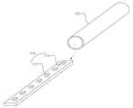
도 1은 실시 예에 따른 발광소자 어레이를 나타내는 사시도이고, 도 2는 도 1에 나타낸 발광소자를 나타내는 단면도이다.FIG. 1 is a perspective view showing a light emitting element array according to an embodiment, and FIG. 2 is a sectional view showing the light emitting element shown in FIG.
도 1 및 도 2를 참조하면, 발광소자 어레이(100)는, 발광소자(112) 및 발광소자(212)가 실장되는 인쇄회로기판(114) 및 발광소자(112)와 인쇄회로기판(114)을 밀봉하는 밀봉부재(120)를 포함한다.1 and 2, the light emitting device array 100 includes a printed
여기서, 발광소자(112)는 발광칩(10) 및 발광칩(10)이 실장되는 몸체(25)를 포함한다.The
몸체(25)는 외부 전원을 공급받아 발광칩(21)에 공급하기 위한 제1, 2 전극(22, 24)가 형성된다.The
또한, 몸체(25)는 폴리프탈아미드(PPA:Polyphthalamide)와 같은 수지 재질, 실리콘(Si), 알루미늄(Al), 알루미늄 나이트라이드(AlN), AlOx, 액정폴리머(PSG, photo sensitive glass), 폴리아미드9T(PA9T), 신지오택틱폴리스티렌(SPS), 금속 재질, 사파이어(Al2O3), 베릴륨 옥사이드(BeO), 인쇄회로기판(PCB, Printed Circuit Board) 중 적어도 하나로 형성될 수 있다. 몸체(25)는 사출 성형, 에칭 공정 등에 의해 형성될 수 있으나 이에 대해 한정하지는 않는다.The
여기서, 제1, 2 전극(22, 24)은 금속 재질, 예를 들어, 티타늄(Ti), 구리(Cu), 니켈(Ni), 금(Au), 크롬(Cr), 탄탈늄(Ta), 백금(Pt), 주석(Sn), 은(Ag), 인(P), 알루미늄(Al), 인듐(In), 팔라듐(Pd), 코발트(Co), 규소(Si), 게르마늄(Ge), 하프늄(Hf), 루테늄(Ru), 철(Fe) 중에서 하나 이상의 물질 또는 합금을 포함할 수 있다. 또한, 제1, 2 전극(22, 24)은 단층 또는 다층 구조를 가지도록 형성될 수 있으며, 이에 대해 한정하지는 않는다.The first and
즉, 몸체(25)는 전도성을 갖는 금속 재질이므로, 몸체(25)의 표면에는 절연막(미도시)이 더 형성되어 몸체(25)가 제1, 2 전극(22, 24)과 전기적으로 쇼트(short) 되는 것을 방지하도록 구성될 수 있다.Since the
몸체(25)의 상면 형상은 발광 소자의 용도 및 설계에 따라 삼각형, 사각형, 다각형, 및 원형 등 다양한 형상을 가질 수 있다.The top surface shape of the
발광칩(10)이 실장되는 몸체(25)에 형성된 캐비티(26)는 단면 형상이 컵 형상, 오목한 용기 형상등으로 형성될 수 있으며, 내측면은 바닥에 대해 수직한 측면이거나 또는 경사진 측면으로 형성될 수 있다.The
그리고, 캐비티(26)의 전면 형상은 원형, 사각형, 다각형, 타원형 등의 형상일 수있으며, 이에 한정을 두지 않는다.The shape of the front surface of the
발광칩(10)은 와이어 본딩(wire bonding) 방식에 의해 제1, 2 전극(22, 24)과 전기적으로 연결될 수 있다.The
즉, 발광칩(10)이 수평형 발광칩일 경우는 제1, 2 전극(22, 24)과 금속 와이어(wire)를 통해 전기적으로 결선될 수 있다.That is, when the
반면에, 발광칩(10)이 수직형 발광칩일 경우, 제2 전극(24) 상에 실장되는 경우는, 제1 전극(22)과 와이어 본딩 처리되고, 제2 전극(24)과는 와이어 본딩 처리되지 않는다.On the other hand, when the
이외에, 발광칩(10)이 플립형 발광칩일 경우, 다이 본딩(die bonding) 방식 등으로 제1, 2 전극(22, 24)과 전기적으로 연결될 수 있다.In addition, when the
한편, 도면에는 자세히 도시하지는 않았으나 캐비티(26)에는 발광칩(10)을 덮도록 봉지재(미도시)가 충진된다.The
여기서, 인쇄회로기판(114)은 인쇄회로기판(114)은 에폭시 기판, 메탈 기판 및 세라믹 기판 중 어느 하나일 수 있으며, 제1, 2 전극(22, 24)과 전기적으로 접촉되는 제1, 2 동박(미도시) 패턴이 형성되어, 발광소자(112)가 상기 제1, 2 동박에 실장되면, 입력되는 전원을 발광소자(112)로 공급한다.The printed
밀봉부재(120)는 인쇄회로기판(114)에 발광소자(112)가 실장된 후, 인쇄회로기판(114)와 발광소자(112)를 밀봉한다.The sealing
이때, 밀봉부재(120)는 열에 의해 수축되는 열수축 튜브이며, 상기 열수축 튜브는 투명재질 또는 다양한 색상을 나타낼 수 있는 색상이 함유된 재질일 수 있으며, 이에 한정을 두지 않는다.At this time, the sealing
여기서, 밀봉부재(120)는 발광소자(112)의 측면, 즉 몸체(25)의 양측면에 형성된 제1, 2 전극(22, 24)와 인쇄회로기판(114)의 상기 제1, 2 동박패턴 사이에 침습에 의한 부식을 방지할 수 있도록 한다.Here, the sealing
이와 같이, 밀봉부재(120)는 공기 중에 존재하는 습기에 의한 부식을 방지하며, 인쇄회로기판(114)이 메탈 기판인 경우 인쇄회로기판(114)의 층 사이의 부식 또한 방지할 수 있을 것이다.Thus, the sealing
도 1에 나타낸 바와 같이, 인쇄회로기판(114) 상에는 복수 개의 발광소자(112)가 실장될 수 있으며, 또한 하나의 발광소자(112)가 실장될 수 있을 것이다.As shown in FIG. 1, a plurality of
또한, 밀봉부재(120)는 인쇄회로기판(114) 상에 복수의 발광소자(112)가 두 개의 그룹으로 나누어지는 경우, 각 그룹 별로 밀봉할 수 있으며, 적어도 3이상의 그룹으로 나누어지는 경우 인쇄회로기판(114)의 양측 최외곽에 위치한 2개의 그룹만 밀봉 할 수 있을 것이다.When the plurality of
다시말하면, 발광소자 어레이(100)는 측면에서 들어오는 공기에 포함된 습기에 의해 부식이 먼저 진행되므로, 인쇄회로기판(114)의 양측 최외곽 영역에 위치한 발광소자(112) 들을 밀봉하는 것이 바람직할 것이다.In other words, it is preferable to seal the
또한, 밀봉부재(120)는 하나의 인쇄회로기판(114)에 실장된 복수의 발광소자(112) 중 일부 영역에 실장된 발광소자(112)들만 밀봉할 수 있다. 즉, 밀봉부재(120)는 인쇄회로기판(114)의 양측 최외곽 영역을 제외한 주변 영역에 실장된 발광소자(114)를 밀봉함에 있어, 양측 최외곽 영역 보다 공기와의 접촉이 많은 영역에 실장된 발광소자(114)를 밀봉할 수 있을 것이며, 이는 설치 위치 및 공간에 따라 다양하게 사용가능 할 것이다.In addition, the sealing
또한, 밀봉부재(120)는 발광소자(112)과 접촉하는 내측면에 다양한 색상의 형광체를 포함한 필름이 형성될 수 있으며, 이는 다양한 색상의 빛을 발산할 수 있도록 할 수 있으며, 이에 한정을 두지않는다.In addition, the sealing
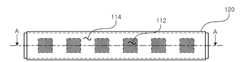
도 3은 제1 실시 예에 따른 발광소자 어레이를 나타내는 평면도이고, 도 4는 도 3에 나타낸 발광소자 어레이의 A-A 단면을 나타내는 단면도이다.FIG. 3 is a plan view showing a light emitting element array according to the first embodiment, and FIG. 4 is a cross-sectional view showing an A-A section of the light emitting element array shown in FIG.
도 3 및 도 4를 참조하면, 발광소자 어레이(100)는 복수 개의 발광소자(112)가 인쇄회로기판(114)에 실장되며, 발광소자(112)와 인쇄회로기판(114)를 밀봉하는 밀봉부재(120)를 포함한다.3 and 4, the light emitting device array 100 includes a plurality of light emitting
밀봉부재(120)는 발광소자(112)와 인쇄회로기판(114)의 둘레를 감싼 후, 챔버(미도시) 내에 삽입되어 상기 챔버에서 발생되는 열에 의해 수축하게 된다.The sealing
따라서, 밀봉부재(120)는 발광소자(112)와 인쇄회로기판(114)을 밀봉하여, 공기가 유입되지 않도록 하여 상기 공기 내에 포함된 습기가 유입되지 않도록 한다.Accordingly, the sealing
도 3에서의 밀봉부재(120)는 인쇄회로기판(114)의 길이보다 짧은 길이로 형성되는 것으로 나타내어 있으나, 인쇄회로기판(114)과 동일한 길이로 형성될 수 있을 것이다.The sealing
여기서, 도 4에 나타낸 발광소자 어레이(100)의 단면을 보면, 발광소자(112)와 인쇄회로기판(114) 그리고 밀봉부재(1200 사이에 소정 공간(S)이 형성됨을 알 수 있다.4 shows that a predetermined space S is formed between the light emitting
즉, 소정 공간(S)은 상기 챔버에 의해 열수축되는 밀봉부재(120)와 발광소자(112)와 인쇄회로기판(114)의 모서리 부분에 생기는 것이며, 진공 상태로 유지될 것이며, 이에 한정을 두지 않는다.That is, the predetermined space S is formed at the corner of the sealing
그리고, 밀봉부재(120)는 발광소자(112)의 모서리 부분에서 곡률을 갖게 된다. 이는, 밀봉부재(120)의 두께에 의해 내측보다 외측에서의 곡률이 크게 됨을 알 수 있다.Then, the sealing
이와 같이, 밀봉부재(120)는 발광소자(112)와 인쇄회로기판(114)에 형성되는 전극, 동박 패턴 등과 같은 금속 또는 전도성 물질로 공기의 유입 및 습기의 유입을 방지하도록 함으로써 부식 등을 방지하도록 하며, 외부 충격에 의해 발광소자(112) 및 인쇄회로기판(114)의 파손을 방지할 수 있는 충격 방지로도 사용될 수 있을 것이다.As described above, the sealing
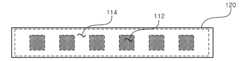
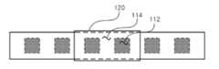
도 5 내지 도 7은 제2 내지 제4 실시 예에 따른 발광소자 어레이를 나타내는 평면도이다.5 to 7 are plan views showing the light emitting element array according to the second to fourth embodiments.
도 5 내지 도 7은 도 3 및 도 4와 중복되는 내용에 대하여 간략하게 설명하거나 생략한다. 5 to 7 will briefly explain or omit the contents overlapping with FIG. 3 and FIG.
도 5에 나타낸 바와 같이, 밀봉부재(120)는 인쇄회로기판(114)의 길이보다 길게 형성되며, 발광소자(112)가 실장된 인쇄회로기판(114) 전체를 밀봉하게 된다.5, the sealing
이와 같이, 밀봉부재(120)는 인쇄회로기판(114) 전체를 밀봉함에 따라, 실질적으로 공기의 유입을 차단할 수 있을 것이다. 물론, 밀봉부재(120)는 상기 챔버에 의해 열수축되지만 인쇄회로기판(114)의 양 끝단에서 완벽하게 밀봉되지 않을 수 있을 것이다.Thus, as the sealing
도 6 및 도 7에 나타낸 밀봉부재(120)는 인쇄회로기판(114)의 일부 영역 만을 밀봉한다.The sealing
즉, 도 6에 나타낸 밀봉부재(120)는 인쇄회로기판(114)의 양측 모서리 영역을 밀봉한다. 즉, 인쇄회로기판(114)은 대체적으로 공기중에 개방된 상태로 위치하는 경우보단 케이스에 의해 일차적으로 공기의 유입이 방지되도록 한다.That is, the sealing
하지만, 인쇄회로기판(114)의 양측 모서리 영역은 공기의 유입이 다른 영역에 비하여 크게 되므로, 발광소자(112) 및 인쇄회로기판(114)의 부식이 다른 영역에 비하여 크게 발생할 수 있는 확률이 높게 되기 때문이다.However, since the inflow of air into both side edge regions of the printed
따라서, 도 6에 나타낸 밀봉부재(120)는 양측 모서리 영역 만을 밀봉하도록 한다.Therefore, the sealing
도 7에 나타낸 밀봉부재(120)는 도 6과는 반대로 인쇄회로기판(114)의 양측 모서리 영역을 제외한 다른 영역, 즉 중앙 영역을 밀봉한다.The sealing
밀봉부재(120)는 인쇄회로기판(114)의 중앙 영역에 실장된 발광소자(112)가 충격에 의한 파손을 방지하기 위함이며, 인쇄회로기판(114)의 중앙 영역에 위치한 발광소자(112)가 조명 장치 또는 백라이트 장치에서의 광효율 측면에서 중요하기 때문이다.The sealing
따라서, 실시 예에 따른 발광소자 어레이는 밀봉부재를 통하여 외부 충격 및 외부 습기의 유입을 방지하도록 함으로써, 발광소자 및 인쇄회로기판의 신뢰성 및 수명 연장에 대한 이점이 있다.Therefore, the light emitting device array according to the embodiment has an advantage in that reliability and life span of the light emitting device and the printed circuit board are improved by preventing external shock and external moisture from flowing through the sealing member.
도 8은 본 발명에 따른 조명장치를 나타내는 사시도이며, 도 9는 도 8에 나타낸 조명장치의 A-A' 단면을 나타내는 단면도이다.FIG. 8 is a perspective view showing a lighting apparatus according to the present invention, and FIG. 9 is a sectional view showing a section taken along the line A-A 'of the lighting apparatus shown in FIG.
즉, 도 9는 도 8의 조명장치(200)를 길이방향(Z)과 높이방향(X)의 면으로 자르고, 수평방향(Y)으로 바라본 단면도이다.9 is a cross-sectional view of the lighting apparatus 200 of FIG. 8 cut in the longitudinal direction Z and the height direction X and viewed in the horizontal direction Y. As shown in FIG.
도 8 및 도 9를 참조하면, 본 조명장치(200)는 몸체(210), 몸체(210)와 체결되는 커버(230) 및 몸체(210)의 양단에 위치하는 마감캡(250)을 포함한다.8 and 9, the lighting apparatus 200 includes a body 210, a cover 230 coupled to the body 210, and a finishing cap 250 positioned at both ends of the body 210 .
몸체(210)의 하부면에는 발광소자 어레이(240)가 체결되며, 몸체(210)는 발광소자(244)에서 발생 된 열이 몸체(210)의 상부면을 통하여 외부로 방출할 수 있도록 전도성 및 열 발산 효과가 우수한 금속재질로 형성될 수 있다.The light emitting device array 240 is coupled to the lower surface of the body 210. The body 210 is electrically connected to the light emitting device 244 so that heat generated from the light emitting device 244 can be emitted to the outside through the upper surface of the body 210. [ It can be formed of a metal material having excellent heat dissipation effect.
발광소자 어레이(240)는 도 1에 나타낸 발광소자 어레이(100)임을 명시한다.The light emitting element array 240 specifies the light emitting element array 100 shown in FIG.
발광소자(244)는 인쇄회로기판(242) 상에 다색, 다열로 실장 될 수 있으며, 동일한 간격으로 체결 고정되거나 또는 필요에 따라 다양한 이격 거리를 가지고 체결 고정 될 수 있어 밝기 등을 조절할 수 있다. 또한, 효과적인 방열을 위해 인쇄회로기판(242)은 금속(Metal) 기판일 수 있다.The light emitting devices 244 may be mounted on the printed circuit board 242 in multiple colors, in multiple rows, and may be fastened or fixed at equal intervals, or may be fastened and fixed with various spacings as required. In addition, the printed circuit board 242 may be a metal substrate for effective heat dissipation.
한편, 도 9를 참조하면, 인쇄회로기판(242)은 바닥면 전체가 몸체(210)에 접하여 체결되므로, 보다 효과적으로 발광소자(244)에서 발생한 열이 몸체(210)로 전도될 수 있다.9, since the entire bottom surface of the printed circuit board 242 is brought into contact with the body 210, the heat generated by the light emitting element 244 can be conducted to the body 210 more effectively.
커버(230)는 몸체(210)의 하부면을 감싸도록 원형의 형태로 형성될 수 있으나, 이에 한정하지 않는다.The cover 230 may be formed in a circular shape so as to surround the lower surface of the body 210, but is not limited thereto.
커버(230)는 내부의 발광소자 어레이(240)를 외부의 이물질 등으로부터 보호한다. 또한, 커버(230)는 발광소자(244)에서 발생한 광의 눈부심을 방지하고, 외부로 광을 균일하게 방출할 수 있도록 확산입자를 포함할 수 있으며, 또한 커버(230)의 내면 및 외면 중 적어도 어느 한 면에는 프리즘 패턴 등이 형성될 수 있다.The cover 230 protects the internal light emitting device array 240 from foreign substances or the like. The cover 230 may include diffusion particles to prevent glare of light generated by the light emitting device 244 and uniformly emit light to the outside, and may include at least one of an inner surface and an outer surface of the cover 230 A prism pattern or the like may be formed on one side.
한편, 발광소자(244)에서 발생한 광은 커버(230)를 통해 외부로 방출되므로 커버(230)는 광투과율이 우수하여야 하며, 발광소자(244)에서 발생한 열에 견딜 수 있도록 충분한 내열성을 구비하고 있어야 하는바, 커버(230)는 폴리에틸렌 테레프탈레이트(Polyethylen Terephthalate; PET), 폴리카보네이트(Polycarbonate; PC) 또는 폴리메틸 메타크릴레이트(Polymethyl Methacrylate; PMMA) 등을 포함하는 재질로 형성되는 것이 바람직하다.Since the light emitted from the light emitting element 244 is emitted to the outside through the cover 230, the cover 230 should have a high light transmittance and sufficient heat resistance to withstand the heat generated by the light emitting element 244 The cover 230 is formed of a material including polyethylene terephthalate (PET), polycarbonate (PC), or polymethyl methacrylate (PMMA).
마감캡(250)은 몸체(210)의 양단에 위치하며 전원장치(미도시)를 밀폐하는 용도로 사용될 수 있다. 또한, 마감캡(250)에는 전원핀(252)이 형성되어 있어, 본 발명에 따른 조명장치(200)는 기존의 형광등을 제거한 단자에 별도의 장치 없이 곧바로 사용할 수 있게 된다.The finishing cap 250 is positioned at both ends of the body 210 and can be used to seal a power supply unit (not shown). In addition, the finishing cap 250 is formed with the power pin 252, so that the lighting device 200 according to the present invention can be used immediately without a separate device on the terminal from which the conventional fluorescent lamp is removed.
도 10은 실시 예에 따른 발광소자 어레이를 포함하는 백라이트 장치에 대한 제1 실시 예를 나타낸 사시도이다.10 is a perspective view illustrating a first embodiment of a backlight device including a light emitting device array according to an embodiment.
도 10은 수직형 백라이트 장치를 나타내며, 도 10을 참조하면 백라이트 장치는 하부 수납 부재(350), 반사판(320), 복수의 발광소자모듈(340) 및 다수의 광학 시트(330)를 포함할 수 있다.10 illustrates a vertical type backlight device. Referring to FIG. 10, the backlight device may include a lower receiving member 350, a reflector 320, a plurality of light emitting device modules 340, and a plurality of optical sheets 330 have.
이때, 발광소자모듈(340)은 복수의 발광소자(344)와 복수의 발광소자(344)가 실장되어 어레이를 이룰 수 있도록 인쇄회로기판(342)을 포함할 수 있다.At this time, the light emitting device module 340 may include a printed circuit board 342 so that a plurality of light emitting devices 344 and a plurality of light emitting devices 344 are mounted to form an array.
한편, 발광소자 (344)의 바닥면에는 다수의 돌기 등이 형성될 수도 있어, 적색 광, 녹색 광 및 청색 광의 색 혼합효과를 향상시킬 수 있다.On the other hand, a plurality of protrusions or the like may be formed on the bottom surface of the light emitting device 344, thereby improving the color mixing effect of red light, green light, and blue light.
반사판(320)은 높은 광 반사율을 갖는 플레이트를 사용하여 광손실을 줄일 수 있다. 광학 시트(330)는 휘도 향상 시트(332), 프리즘 시트(334) 및 확산시트(336) 중 적어도 하나를 포함할 수 있다.The reflector 320 can reduce light loss by using a plate having a high light reflectivity. The optical sheet 330 may include at least one of the brightness enhancement sheet 332, the prism sheet 334, and the diffusion sheet 336. [
확산 시트(336)는 발광소자모듈(340)로부터 입사된 광을 액정 표시 패널(미도시)의 정면으로 향하게 하고, 넓은 범위에서 균일한 분포를 가지도록 광을 확산시켜 액정 표시 패널(미도시)에 조사할 수 있다. 프리즘 시트(334)는 프리즘 시트(334)로 입사되는 광들 중에서 경사지게 입사되는 광을 수직으로 출사되게 변화시키는 역할을 한다. 즉, 확산 시트(336)로부터 출사되는 광을 수직으로 변환시키기 위해 적어도 하나의 프리즘 시트(334)를 액정 표시 패널(미도시) 하부에 배치시킬 수 있다. 휘도 향상 시트(332)는 자신의 투과축과 나란한 광은 투과시키고 투과축에 수직한 광은 반사시킨다.The diffusion sheet 336 directs the light incident from the light emitting element module 340 toward the front surface of a liquid crystal display panel (not shown), and diffuses light so as to have a uniform distribution over a wide range to form a liquid crystal display panel (not shown) . The prism sheet 334 serves to vertically emit light incident on the prism sheet 334 obliquely. That is, at least one prism sheet 334 may be disposed below the liquid crystal display panel (not shown) to vertically convert the light emitted from the diffusion sheet 336. The brightness enhancement sheet 332 transmits light parallel to its transmission axis and reflects light perpendicular to the transmission axis.
도 11은 실시예에 따른 발광소자 어레이를 포함하는 백라이트 장치에 대한 제2 실시 예를 나타낸 사시도이다.11 is a perspective view illustrating a backlight device including a light emitting device array according to a second embodiment of the present invention.
도 11은 엣지형 백라이트 장치을 도시하며, 도 11을 참조하면 백라이트 장치는 하부 수납 부재(400), 빛을 출력하는 발광소자모듈(410), 발광소자모듈(410)에 인접 배치된 도광판(420) 및 다수의 광학 시트(미도시)를 포함할 수 있다. 다수의 광학 시트(미도시)는 도광판(420) 상에 위치할 수 있으며, 이는 도 10에서 나타내고 설명한 다수의 광학 시트(430)와 동일하므로 자세한 설명은 생략하기로 한다.11, the backlight device includes a lower receiving member 400, a light emitting device module 410 for outputting light, a light guide plate 420 disposed adjacent to the light emitting device module 410, And a plurality of optical sheets (not shown). A plurality of optical sheets (not shown) may be positioned on the light guide plate 420, which is the same as the plurality of optical sheets 430 illustrated and described with reference to FIG. 10, and thus a detailed description thereof will be omitted.
발광소자모듈(410)은 복수의 발광소자(414)가 인쇄회로기판(412)상에 실장되어 어레이를 이룰 수 있다. 이러한 인쇄회로기판(412)으로는 MCPCB(Metal Core PCB) 또는 FR4 재질의 PCB를 사용할 수 있다. 또한 인쇄회로기판(412)은 사각 판 형태뿐만 아니라 백라이트 어셈블리의 구조에 따라 다양한 형태로의 제작이 가능하다.In the light emitting device module 410, a plurality of light emitting devices 414 may be mounted on the printed circuit board 412 to form an array. As the printed circuit board 412, MCPCB (Metal Core PCB) or FR4 PCB may be used. In addition, the printed circuit board 412 can be manufactured in various shapes according to the structure of the backlight assembly as well as the shape of the square plate.
도광판(420)은 발광소자(414)에서 출력한 빛을 면광원 형태로 변경시켜 액정표시패널(미도시)로 제공하며, 도광판(420)으로부터 제공된 빛의 휘도 분포를 균일하게 만들고 수직 입사성을 향상시키는 다수의 광학 필름(미도시) 및 도광판(420)의 후방으로 방출되는 빛을 도광판(420)으로 반사시키는 반사 시트(미도시)가 도광판(620)의 배면에 위치할 수 있다.The light guide plate 420 changes the light output from the light emitting element 414 into a surface light source to provide the light to the liquid crystal display panel (not shown), uniformizes the luminance distribution of light provided from the light guide plate 420, And a reflective sheet (not shown) for reflecting the light emitted to the rear of the light guide plate 420 by the light guide plate 420 may be positioned on the back surface of the light guide plate 620. [
한편, 도 10에서 나타내고 설명한 수직형 백라이트 장치의 구조와 도 11에서 나타내고 설명한 엣지형 백라이트 장치의 구조는 혼합하여 사용이 가능함할 것이다.The structure of the vertical type backlight device shown in FIG. 10 and the structure of the edge type backlight device shown in FIG. 11 may be used in combination.
이상에서 실시예들에 설명된 특징, 구조, 효과 등은 본 발명의 적어도 하나의 실시예에 포함되며, 반드시 하나의 실시예에만 한정되는 것은 아니다. 나아가, 각 실시예에서 예시된 특징, 구조, 효과 등은 실시예들이 속하는 분야의 통상의 지식을 가지는 자에 의해 다른 실시예들에 대해서도 조합 또는 변형되어 실시 가능하다. 따라서 이러한 조합과 변형에 관계된 내용들은 본 발명의 범위에 포함되는 것으로 해석되어야 할 것이다.The features, structures, effects and the like described in the embodiments are included in at least one embodiment of the present invention and are not necessarily limited to only one embodiment. Furthermore, the features, structures, effects and the like illustrated in the embodiments can be combined and modified by other persons skilled in the art to which the embodiments belong. Therefore, it should be understood that the present invention is not limited to these combinations and modifications.
또한, 이상에서 실시예를 중심으로 설명하였으나 이는 단지 예시일 뿐 본 발명을 한정하는 것이 아니며, 본 발명이 속하는 분야의 통상의 지식을 가진 자라면 본 실시예의 본질적인 특성을 벗어나지 않는 범위에서 이상에 예시되지 않은 여러가지의 변형과 응용이 가능함을 알 수 있을 것이다. 예를 들어, 실시예에 구체적으로 나타난 각 구성 요소는 변형하여 실시할 수 있는 것이다. 그리고 이러한 변형과 응용에 관계된 차이점들은 첨부된 청구 범위에서 규정하는 본 발명의 범위에 포함되는 것으로 해석되어야 할 것이다.While the present invention has been particularly shown and described with reference to exemplary embodiments thereof, it is clearly understood that the same is by way of illustration and example only and is not to be taken by way of illustration, It will be appreciated that various modifications and applications are possible without departing from the scope of the present invention. For example, each component specifically shown in the embodiments can be modified and implemented. It is to be understood that all changes and modifications that come within the meaning and range of equivalency of the claims are therefore intended to be embraced therein.
Claims (11)
Translated fromKorean상기 발광소자가 실장되는 인쇄회로기판; 및
상기 발광소자 및 상기 인쇄회로기판을 감싸는 열수축 튜브로 구성되는 밀봉부재;를 포함하고,
상기 발광소자는
발광칩; 상기 발광칩이 실장되는 몸체; 상기 몸체에 형성되는 제1, 2전극; 및
상기 몸체에 형성되는 캐비티; 를 포함하고,
상기 밀봉 부재는
열에 의해 수축되어 상기 인쇄회로 기판의 전체 또는 일부 영역인 상기 인쇄회로기판의 양측 가장자리의 모서리 영역이나, 상기 양측 가장자리 영역을 제외한 중앙 영역을 밀봉하고, 상기 열에 의해 수축된 상기 밀봉부재와 상기 인쇄회로기판 또는 상기 발광소자 사이에 소정 공간이 형성되고, 상기 열에 의해 수축된 상기 밀봉부재는 상기 인쇄회로기판 또는 상기 발광소자의 모서리 부분에서 곡률을 갖는 것을 특징으로 하는 발광소자 어레이.
A light emitting element;
A printed circuit board on which the light emitting device is mounted; And
And a sealing member composed of a heat shrinkable tube surrounding the light emitting device and the printed circuit board,
The light-
A light emitting chip; A body on which the light emitting chip is mounted; First and second electrodes formed on the body; And
A cavity formed in the body; Lt; / RTI >
The sealing member
A sealing member which is contracted by heat to seal a corner region of both side edges of the printed circuit board, which is all or a part of the printed circuit board, or a central region excluding the both side edge regions, Wherein a predetermined space is formed between the substrate and the light emitting element, and the sealing member contracted by the heat has a curvature at corner portions of the printed circuit board or the light emitting element.
적어도 2이상인 것을 특징으로 하는 발광소자 어레이.The light emitting device according to claim 1,
And at least two light emitting element arrays.
투명한 것을 특징으로 하는 발광소자 어레이.The seal member according to claim 1,
Wherein the light emitting element array is transparent.
색상을 갖는 것을 특징으로 하는 발광소자 어레이.The seal member according to claim 1,
Wherein the light emitting element array has a color.
A backlight device comprising the light-emitting element array according to any one of claims 1 to 9.
Priority Applications (5)
| Application Number | Priority Date | Filing Date | Title |
|---|---|---|---|
| KR1020100044602AKR101641860B1 (en) | 2010-05-12 | 2010-05-12 | Light-emitting element array, Backlight apparatus, and Illumination apparatus |
| EP11161815.3AEP2386790B1 (en) | 2010-05-12 | 2011-04-11 | Light emitting device module |
| US13/085,945US9285083B2 (en) | 2010-05-12 | 2011-04-13 | Light emitting device module |
| CN2011101237881ACN102244072B (en) | 2010-05-12 | 2011-05-10 | Light emitting device module |
| JP2011107365AJP2011238933A (en) | 2010-05-12 | 2011-05-12 | Light emitting device module and illumination system |
Applications Claiming Priority (1)
| Application Number | Priority Date | Filing Date | Title |
|---|---|---|---|
| KR1020100044602AKR101641860B1 (en) | 2010-05-12 | 2010-05-12 | Light-emitting element array, Backlight apparatus, and Illumination apparatus |
Publications (2)
| Publication Number | Publication Date |
|---|---|
| KR20110125064A KR20110125064A (en) | 2011-11-18 |
| KR101641860B1true KR101641860B1 (en) | 2016-07-29 |
Family
ID=44509792
Family Applications (1)
| Application Number | Title | Priority Date | Filing Date |
|---|---|---|---|
| KR1020100044602AExpired - Fee RelatedKR101641860B1 (en) | 2010-05-12 | 2010-05-12 | Light-emitting element array, Backlight apparatus, and Illumination apparatus |
Country Status (5)
| Country | Link |
|---|---|
| US (1) | US9285083B2 (en) |
| EP (1) | EP2386790B1 (en) |
| JP (1) | JP2011238933A (en) |
| KR (1) | KR101641860B1 (en) |
| CN (1) | CN102244072B (en) |
Families Citing this family (9)
| Publication number | Priority date | Publication date | Assignee | Title |
|---|---|---|---|---|
| US20130032828A1 (en)* | 2011-08-02 | 2013-02-07 | Hsu Takeho | Led light strip module structure |
| DE102012204510A1 (en)* | 2011-11-18 | 2013-05-23 | Tridonic Jennersdorf Gmbh | Tubular LED lamp |
| JP6201480B2 (en)* | 2013-07-23 | 2017-09-27 | 日亜化学工業株式会社 | Light emitting device and lighting device |
| JP2015167090A (en)* | 2014-03-03 | 2015-09-24 | パナソニックIpマネジメント株式会社 | Light source of lighting and lighting device |
| DE202014005059U1 (en)* | 2014-06-17 | 2014-09-10 | Petrus Pfundt | Tubelight LED light tube |
| DE102016122127A1 (en)* | 2016-08-18 | 2018-02-22 | Ledvance Gmbh | Clean room lighting based on LEDs |
| DE202019101941U1 (en)* | 2019-04-04 | 2019-04-10 | Herrnhuter Sterne GmbH | Electric candle |
| AU2019473094A1 (en) | 2019-11-04 | 2022-02-17 | Northquip Inc. | Portable livestock handling apparatus with foldable force tub and extendable/collapsible chassis |
| FI20236085A1 (en)* | 2023-09-28 | 2025-03-29 | Greenlux Lighting Solutions Oy | Led-based lighting device |
Citations (3)
| Publication number | Priority date | Publication date | Assignee | Title |
|---|---|---|---|---|
| JP2004095853A (en) | 2002-08-30 | 2004-03-25 | Koha Co Ltd | Led lamp and lighting device |
| JP2004207341A (en)* | 2002-12-24 | 2004-07-22 | Sanken Electric Co Ltd | Emitted light wavelength converting semiconductor light emitting device and its manufacturing method |
| JP3143340U (en) | 2007-11-09 | 2008-07-17 | 樹發 邵 | Lighting device |
Family Cites Families (51)
| Publication number | Priority date | Publication date | Assignee | Title |
|---|---|---|---|---|
| ATE47624T1 (en)* | 1984-11-15 | 1989-11-15 | Japan Traffic Manage Tech Ass | SIGNAL LIGHT UNIT WITH HEAT DISSIPATION. |
| FR2650153B1 (en)* | 1989-07-28 | 1994-04-01 | Mitchell Sports | DEVICE FOR FIXING, ADJUSTABLY, AN ACCESSORY SUCH AS A REEL ON A FISHING ROD |
| JPH03120714A (en)* | 1989-10-04 | 1991-05-22 | Toshiba Corp | X-ray exposure device |
| US5276599A (en)* | 1992-02-21 | 1994-01-04 | Neeley Willard L | Light sculpture device |
| NO176415C (en)* | 1992-10-16 | 1995-03-29 | Technor As | Level moldings |
| US5412159A (en)* | 1993-09-27 | 1995-05-02 | Zenith Electronics Corporation | High voltage resistive network circuit board with good potting adhesion |
| US5410328A (en)* | 1994-03-28 | 1995-04-25 | Trans-Lux Corporation | Replaceable intelligent pixel module for large-scale LED displays |
| TW408497B (en)* | 1997-11-25 | 2000-10-11 | Matsushita Electric Works Ltd | LED illuminating apparatus |
| US6152590A (en)* | 1998-02-13 | 2000-11-28 | Donnelly Hohe Gmbh & Co. Kg | Lighting device for motor vehicles |
| JP3925602B2 (en)* | 1999-06-14 | 2007-06-06 | セイコーエプソン株式会社 | Adhesive material attaching method and semiconductor device manufacturing method |
| US7401935B2 (en)* | 1999-09-17 | 2008-07-22 | Vanderschuit Carl R | Beverage accessory devices |
| JP2002006325A (en)* | 2000-06-20 | 2002-01-09 | Nec Corp | Method for manufacturing liquid crystal display panel |
| JP3554533B2 (en)* | 2000-10-13 | 2004-08-18 | シャープ株式会社 | Chip-on-film tape and semiconductor device |
| US6639360B2 (en)* | 2001-01-31 | 2003-10-28 | Gentex Corporation | High power radiation emitter device and heat dissipating package for electronic components |
| US8376576B2 (en)* | 2001-07-25 | 2013-02-19 | The Sloan Company, Inc. | Perimeter lighting |
| JPWO2003032064A1 (en)* | 2001-10-03 | 2005-01-27 | 松下電器産業株式会社 | LCD panel |
| US7192161B1 (en)* | 2001-10-18 | 2007-03-20 | Ilight Technologies, Inc. | Fluorescent illumination device |
| TW533750B (en)* | 2001-11-11 | 2003-05-21 | Solidlite Corp | LED lamp |
| US20030090892A1 (en)* | 2001-11-13 | 2003-05-15 | Chin-Lai Su | Drinking vessel capable of emitting light and sound |
| WO2003071843A1 (en)* | 2002-02-22 | 2003-08-28 | Fujikura Ltd. | Multilayer wiring board, base for multilayer wiring board, printed wiring board, and its manufacturing method |
| US6758993B2 (en)* | 2002-04-17 | 2004-07-06 | Delphi Technologies, Inc. | System and method for minimizing cure-induced residual stress in an epoxy impregnated ignition coil |
| US7800121B2 (en)* | 2002-08-30 | 2010-09-21 | Lumination Llc | Light emitting diode component |
| JP4252297B2 (en)* | 2002-12-12 | 2009-04-08 | 株式会社日立製作所 | LIGHT EMITTING ELEMENT AND DISPLAY DEVICE USING THE LIGHT EMITTING ELEMENT |
| TWI352553B (en)* | 2002-12-26 | 2011-11-11 | Semiconductor Energy Lab | Light emitting device and a method for manufacturi |
| TWI235506B (en)* | 2003-12-02 | 2005-07-01 | Yuan Lin | Light reflection device and its manufacturing method |
| US7245279B2 (en)* | 2003-12-04 | 2007-07-17 | Xiao-Ping Wang | Linear led array |
| US20050270774A1 (en)* | 2004-06-03 | 2005-12-08 | Frank Pan | LED illuminating strip unit |
| JP4802533B2 (en)* | 2004-11-12 | 2011-10-26 | 日亜化学工業株式会社 | Semiconductor device |
| JP4828886B2 (en) | 2005-07-29 | 2011-11-30 | 株式会社光波 | Surface light emitting module and surface light emitting device using the same |
| JP2007081234A (en)* | 2005-09-15 | 2007-03-29 | Toyoda Gosei Co Ltd | Lighting system |
| JP3120714U (en) | 2006-01-17 | 2006-04-20 | 森山産業株式会社 | LED lighting device |
| DE102006031345A1 (en)* | 2006-07-06 | 2008-01-10 | Patent-Treuhand-Gesellschaft für elektrische Glühlampen mbH | Shapely flexible lighting system |
| US7887218B2 (en)* | 2006-10-17 | 2011-02-15 | Baoliang Wang | LED illuminating device |
| US7889421B2 (en)* | 2006-11-17 | 2011-02-15 | Rensselaer Polytechnic Institute | High-power white LEDs and manufacturing method thereof |
| EP1928026A1 (en)* | 2006-11-30 | 2008-06-04 | Toshiba Lighting & Technology Corporation | Illumination device with semiconductor light-emitting elements |
| JP4893582B2 (en)* | 2007-10-25 | 2012-03-07 | 豊田合成株式会社 | Light source device |
| US7810954B2 (en)* | 2007-12-03 | 2010-10-12 | Lumination Llc | LED-based changeable color light lamp |
| JP5133120B2 (en) | 2008-04-24 | 2013-01-30 | シチズン電子株式会社 | Light emitting device |
| US7618157B1 (en)* | 2008-06-25 | 2009-11-17 | Osram Sylvania Inc. | Tubular blue LED lamp with remote phosphor |
| JP2010010437A (en) | 2008-06-27 | 2010-01-14 | Stanley Electric Co Ltd | Optical semiconductor device |
| US20100078483A1 (en)* | 2008-09-26 | 2010-04-01 | Rong Liu | Arrangement for and method of generating uniform distributed line pattern for imaging reader |
| KR100993059B1 (en)* | 2008-09-29 | 2010-11-08 | 엘지이노텍 주식회사 | Light emitting device |
| JP2010103355A (en) | 2008-10-24 | 2010-05-06 | Alpine Electronics Inc | Led module for backlight |
| CN101749640B (en)* | 2008-12-05 | 2012-12-26 | 富准精密工业(深圳)有限公司 | Light emitting diode lamp |
| CN101482252B (en)* | 2008-12-08 | 2010-10-13 | 上海三思电子工程有限公司 | Convection cooling type LED illumination device |
| US8556452B2 (en)* | 2009-01-15 | 2013-10-15 | Ilumisys, Inc. | LED lens |
| TWM368029U (en)* | 2009-03-30 | 2009-11-01 | E Pin Internat Tech Co Ltd | Fresnel LED lens and LED assembly thereof |
| US8348460B2 (en)* | 2009-05-01 | 2013-01-08 | Abl Ip Holding Llc | Lighting apparatus with several light units arranged in a heatsink |
| CN101994933B (en)* | 2009-08-14 | 2013-01-09 | 鸿富锦精密工业(深圳)有限公司 | Illuminating device |
| US8414149B2 (en)* | 2009-08-25 | 2013-04-09 | Daktronics, Inc. | Light element seal module and method for same |
| US8421111B2 (en)* | 2010-12-27 | 2013-04-16 | Panasonic Corporation | Light-emitting device and lamp |
- 2010
- 2010-05-12KRKR1020100044602Apatent/KR101641860B1/ennot_activeExpired - Fee Related
- 2011
- 2011-04-11EPEP11161815.3Apatent/EP2386790B1/ennot_activeNot-in-force
- 2011-04-13USUS13/085,945patent/US9285083B2/ennot_activeExpired - Fee Related
- 2011-05-10CNCN2011101237881Apatent/CN102244072B/ennot_activeExpired - Fee Related
- 2011-05-12JPJP2011107365Apatent/JP2011238933A/enactivePending
Patent Citations (3)
| Publication number | Priority date | Publication date | Assignee | Title |
|---|---|---|---|---|
| JP2004095853A (en) | 2002-08-30 | 2004-03-25 | Koha Co Ltd | Led lamp and lighting device |
| JP2004207341A (en)* | 2002-12-24 | 2004-07-22 | Sanken Electric Co Ltd | Emitted light wavelength converting semiconductor light emitting device and its manufacturing method |
| JP3143340U (en) | 2007-11-09 | 2008-07-17 | 樹發 邵 | Lighting device |
Also Published As
| Publication number | Publication date |
|---|---|
| CN102244072B (en) | 2013-12-25 |
| EP2386790B1 (en) | 2017-06-07 |
| EP2386790A2 (en) | 2011-11-16 |
| JP2011238933A (en) | 2011-11-24 |
| EP2386790A3 (en) | 2013-09-25 |
| US20110280012A1 (en) | 2011-11-17 |
| US9285083B2 (en) | 2016-03-15 |
| CN102244072A (en) | 2011-11-16 |
| KR20110125064A (en) | 2011-11-18 |
Similar Documents
| Publication | Publication Date | Title |
|---|---|---|
| KR101641860B1 (en) | Light-emitting element array, Backlight apparatus, and Illumination apparatus | |
| CN109983590B (en) | Light emitting device package and light source unit | |
| KR101813495B1 (en) | Light Emitting Diode Package | |
| KR101824011B1 (en) | Light-emitting device | |
| KR101694175B1 (en) | Light emitting device, light emitting device package and lighting system | |
| KR20130098048A (en) | Light emitting device package | |
| KR101659355B1 (en) | Light-emitting element package | |
| KR101831283B1 (en) | Light Emitting Diode Package | |
| KR101824886B1 (en) | Light emitting device package | |
| KR101550938B1 (en) | Light-emitting element package | |
| KR20110125067A (en) | The light- | |
| KR20120130957A (en) | Light emitting device package | |
| KR101781043B1 (en) | Light-emitting element array | |
| KR102075522B1 (en) | Light-emitting device | |
| KR20130117572A (en) | Light emitting device package and backlight unit thereof | |
| KR102119817B1 (en) | Light emitting device | |
| KR101818752B1 (en) | Light emitting device array | |
| KR20110108097A (en) | Light emitting device package and lighting system including same | |
| KR101831276B1 (en) | Light Emitting Diode Package | |
| KR101883344B1 (en) | Light Emitting Device Array | |
| KR20130038558A (en) | Light emitting device | |
| KR102432215B1 (en) | Light unit and lighting apparatus having the same | |
| KR20120071150A (en) | Light emitting device package | |
| KR101778151B1 (en) | Light emitting device package | |
| KR101766717B1 (en) | Light Emitting Device Package |
Legal Events
| Date | Code | Title | Description |
|---|---|---|---|
| PA0109 | Patent application | St.27 status event code:A-0-1-A10-A12-nap-PA0109 | |
| PG1501 | Laying open of application | St.27 status event code:A-1-1-Q10-Q12-nap-PG1501 | |
| PN2301 | Change of applicant | St.27 status event code:A-3-3-R10-R13-asn-PN2301 St.27 status event code:A-3-3-R10-R11-asn-PN2301 | |
| P11-X000 | Amendment of application requested | St.27 status event code:A-2-2-P10-P11-nap-X000 | |
| P13-X000 | Application amended | St.27 status event code:A-2-2-P10-P13-nap-X000 | |
| A201 | Request for examination | ||
| PA0201 | Request for examination | St.27 status event code:A-1-2-D10-D11-exm-PA0201 | |
| D13-X000 | Search requested | St.27 status event code:A-1-2-D10-D13-srh-X000 | |
| P22-X000 | Classification modified | St.27 status event code:A-2-2-P10-P22-nap-X000 | |
| D14-X000 | Search report completed | St.27 status event code:A-1-2-D10-D14-srh-X000 | |
| E902 | Notification of reason for refusal | ||
| PE0902 | Notice of grounds for rejection | St.27 status event code:A-1-2-D10-D21-exm-PE0902 | |
| E13-X000 | Pre-grant limitation requested | St.27 status event code:A-2-3-E10-E13-lim-X000 | |
| P11-X000 | Amendment of application requested | St.27 status event code:A-2-2-P10-P11-nap-X000 | |
| P13-X000 | Application amended | St.27 status event code:A-2-2-P10-P13-nap-X000 | |
| E701 | Decision to grant or registration of patent right | ||
| PE0701 | Decision of registration | St.27 status event code:A-1-2-D10-D22-exm-PE0701 | |
| GRNT | Written decision to grant | ||
| PR0701 | Registration of establishment | St.27 status event code:A-2-4-F10-F11-exm-PR0701 | |
| PR1002 | Payment of registration fee | St.27 status event code:A-2-2-U10-U11-oth-PR1002 Fee payment year number:1 | |
| PG1601 | Publication of registration | St.27 status event code:A-4-4-Q10-Q13-nap-PG1601 | |
| P22-X000 | Classification modified | St.27 status event code:A-4-4-P10-P22-nap-X000 | |
| P22-X000 | Classification modified | St.27 status event code:A-4-4-P10-P22-nap-X000 | |
| R18-X000 | Changes to party contact information recorded | St.27 status event code:A-5-5-R10-R18-oth-X000 | |
| R18-X000 | Changes to party contact information recorded | St.27 status event code:A-5-5-R10-R18-oth-X000 | |
| FPAY | Annual fee payment | Payment date:20190612 Year of fee payment:4 | |
| PR1001 | Payment of annual fee | St.27 status event code:A-4-4-U10-U11-oth-PR1001 Fee payment year number:4 | |
| P22-X000 | Classification modified | St.27 status event code:A-4-4-P10-P22-nap-X000 | |
| R18-X000 | Changes to party contact information recorded | St.27 status event code:A-5-5-R10-R18-oth-X000 | |
| PR1001 | Payment of annual fee | St.27 status event code:A-4-4-U10-U11-oth-PR1001 Fee payment year number:5 | |
| PN2301 | Change of applicant | St.27 status event code:A-5-5-R10-R13-asn-PN2301 St.27 status event code:A-5-5-R10-R11-asn-PN2301 | |
| PR1001 | Payment of annual fee | St.27 status event code:A-4-4-U10-U11-oth-PR1001 Fee payment year number:6 | |
| PN2301 | Change of applicant | St.27 status event code:A-5-5-R10-R11-asn-PN2301 | |
| PN2301 | Change of applicant | St.27 status event code:A-5-5-R10-R14-asn-PN2301 | |
| PR1001 | Payment of annual fee | St.27 status event code:A-4-4-U10-U11-oth-PR1001 Fee payment year number:7 | |
| PC1903 | Unpaid annual fee | St.27 status event code:A-4-4-U10-U13-oth-PC1903 Not in force date:20230719 Payment event data comment text:Termination Category : DEFAULT_OF_REGISTRATION_FEE | |
| PC1903 | Unpaid annual fee | St.27 status event code:N-4-6-H10-H13-oth-PC1903 Ip right cessation event data comment text:Termination Category : DEFAULT_OF_REGISTRATION_FEE Not in force date:20230719 | |
| P22-X000 | Classification modified | St.27 status event code:A-4-4-P10-P22-nap-X000 |