KR101641538B1 - Display panel - Google Patents
Display panelDownload PDFInfo
- Publication number
- KR101641538B1 KR101641538B1KR1020080133715AKR20080133715AKR101641538B1KR 101641538 B1KR101641538 B1KR 101641538B1KR 1020080133715 AKR1020080133715 AKR 1020080133715AKR 20080133715 AKR20080133715 AKR 20080133715AKR 101641538 B1KR101641538 B1KR 101641538B1
- Authority
- KR
- South Korea
- Prior art keywords
- sub
- data
- pixel electrode
- data line
- pixel
- Prior art date
- Legal status (The legal status is an assumption and is not a legal conclusion. Google has not performed a legal analysis and makes no representation as to the accuracy of the status listed.)
- Expired - Fee Related
Links
Images


Classifications
- G—PHYSICS
- G09—EDUCATION; CRYPTOGRAPHY; DISPLAY; ADVERTISING; SEALS
- G09G—ARRANGEMENTS OR CIRCUITS FOR CONTROL OF INDICATING DEVICES USING STATIC MEANS TO PRESENT VARIABLE INFORMATION
- G09G3/00—Control arrangements or circuits, of interest only in connection with visual indicators other than cathode-ray tubes
- G09G3/20—Control arrangements or circuits, of interest only in connection with visual indicators other than cathode-ray tubes for presentation of an assembly of a number of characters, e.g. a page, by composing the assembly by combination of individual elements arranged in a matrix no fixed position being assigned to or needed to be assigned to the individual characters or partial characters
- G09G3/34—Control arrangements or circuits, of interest only in connection with visual indicators other than cathode-ray tubes for presentation of an assembly of a number of characters, e.g. a page, by composing the assembly by combination of individual elements arranged in a matrix no fixed position being assigned to or needed to be assigned to the individual characters or partial characters by control of light from an independent source
- G09G3/36—Control arrangements or circuits, of interest only in connection with visual indicators other than cathode-ray tubes for presentation of an assembly of a number of characters, e.g. a page, by composing the assembly by combination of individual elements arranged in a matrix no fixed position being assigned to or needed to be assigned to the individual characters or partial characters by control of light from an independent source using liquid crystals
- G09G3/3611—Control of matrices with row and column drivers
- G09G3/3696—Generation of voltages supplied to electrode drivers
- G—PHYSICS
- G02—OPTICS
- G02F—OPTICAL DEVICES OR ARRANGEMENTS FOR THE CONTROL OF LIGHT BY MODIFICATION OF THE OPTICAL PROPERTIES OF THE MEDIA OF THE ELEMENTS INVOLVED THEREIN; NON-LINEAR OPTICS; FREQUENCY-CHANGING OF LIGHT; OPTICAL LOGIC ELEMENTS; OPTICAL ANALOGUE/DIGITAL CONVERTERS
- G02F1/00—Devices or arrangements for the control of the intensity, colour, phase, polarisation or direction of light arriving from an independent light source, e.g. switching, gating or modulating; Non-linear optics
- G02F1/01—Devices or arrangements for the control of the intensity, colour, phase, polarisation or direction of light arriving from an independent light source, e.g. switching, gating or modulating; Non-linear optics for the control of the intensity, phase, polarisation or colour
- G02F1/13—Devices or arrangements for the control of the intensity, colour, phase, polarisation or direction of light arriving from an independent light source, e.g. switching, gating or modulating; Non-linear optics for the control of the intensity, phase, polarisation or colour based on liquid crystals, e.g. single liquid crystal display cells
- G02F1/133—Constructional arrangements; Operation of liquid crystal cells; Circuit arrangements
- G02F1/1333—Constructional arrangements; Manufacturing methods
- G02F1/1343—Electrodes
- G02F1/134309—Electrodes characterised by their geometrical arrangement
- G02F1/134363—Electrodes characterised by their geometrical arrangement for applying an electric field parallel to the substrate, i.e. in-plane switching [IPS]
- G—PHYSICS
- G02—OPTICS
- G02F—OPTICAL DEVICES OR ARRANGEMENTS FOR THE CONTROL OF LIGHT BY MODIFICATION OF THE OPTICAL PROPERTIES OF THE MEDIA OF THE ELEMENTS INVOLVED THEREIN; NON-LINEAR OPTICS; FREQUENCY-CHANGING OF LIGHT; OPTICAL LOGIC ELEMENTS; OPTICAL ANALOGUE/DIGITAL CONVERTERS
- G02F1/00—Devices or arrangements for the control of the intensity, colour, phase, polarisation or direction of light arriving from an independent light source, e.g. switching, gating or modulating; Non-linear optics
- G02F1/01—Devices or arrangements for the control of the intensity, colour, phase, polarisation or direction of light arriving from an independent light source, e.g. switching, gating or modulating; Non-linear optics for the control of the intensity, phase, polarisation or colour
- G02F1/13—Devices or arrangements for the control of the intensity, colour, phase, polarisation or direction of light arriving from an independent light source, e.g. switching, gating or modulating; Non-linear optics for the control of the intensity, phase, polarisation or colour based on liquid crystals, e.g. single liquid crystal display cells
- G02F1/133—Constructional arrangements; Operation of liquid crystal cells; Circuit arrangements
- G02F1/1333—Constructional arrangements; Manufacturing methods
- G02F1/1343—Electrodes
- G—PHYSICS
- G02—OPTICS
- G02F—OPTICAL DEVICES OR ARRANGEMENTS FOR THE CONTROL OF LIGHT BY MODIFICATION OF THE OPTICAL PROPERTIES OF THE MEDIA OF THE ELEMENTS INVOLVED THEREIN; NON-LINEAR OPTICS; FREQUENCY-CHANGING OF LIGHT; OPTICAL LOGIC ELEMENTS; OPTICAL ANALOGUE/DIGITAL CONVERTERS
- G02F1/00—Devices or arrangements for the control of the intensity, colour, phase, polarisation or direction of light arriving from an independent light source, e.g. switching, gating or modulating; Non-linear optics
- G02F1/01—Devices or arrangements for the control of the intensity, colour, phase, polarisation or direction of light arriving from an independent light source, e.g. switching, gating or modulating; Non-linear optics for the control of the intensity, phase, polarisation or colour
- G02F1/13—Devices or arrangements for the control of the intensity, colour, phase, polarisation or direction of light arriving from an independent light source, e.g. switching, gating or modulating; Non-linear optics for the control of the intensity, phase, polarisation or colour based on liquid crystals, e.g. single liquid crystal display cells
- G02F1/133—Constructional arrangements; Operation of liquid crystal cells; Circuit arrangements
- G02F1/136—Liquid crystal cells structurally associated with a semi-conducting layer or substrate, e.g. cells forming part of an integrated circuit
- G02F1/1362—Active matrix addressed cells
- G02F1/13624—Active matrix addressed cells having more than one switching element per pixel
- G—PHYSICS
- G09—EDUCATION; CRYPTOGRAPHY; DISPLAY; ADVERTISING; SEALS
- G09G—ARRANGEMENTS OR CIRCUITS FOR CONTROL OF INDICATING DEVICES USING STATIC MEANS TO PRESENT VARIABLE INFORMATION
- G09G3/00—Control arrangements or circuits, of interest only in connection with visual indicators other than cathode-ray tubes
- G09G3/20—Control arrangements or circuits, of interest only in connection with visual indicators other than cathode-ray tubes for presentation of an assembly of a number of characters, e.g. a page, by composing the assembly by combination of individual elements arranged in a matrix no fixed position being assigned to or needed to be assigned to the individual characters or partial characters
- G09G3/34—Control arrangements or circuits, of interest only in connection with visual indicators other than cathode-ray tubes for presentation of an assembly of a number of characters, e.g. a page, by composing the assembly by combination of individual elements arranged in a matrix no fixed position being assigned to or needed to be assigned to the individual characters or partial characters by control of light from an independent source
- G09G3/36—Control arrangements or circuits, of interest only in connection with visual indicators other than cathode-ray tubes for presentation of an assembly of a number of characters, e.g. a page, by composing the assembly by combination of individual elements arranged in a matrix no fixed position being assigned to or needed to be assigned to the individual characters or partial characters by control of light from an independent source using liquid crystals
- G09G3/3611—Control of matrices with row and column drivers
- G09G3/3648—Control of matrices with row and column drivers using an active matrix
- G09G3/3659—Control of matrices with row and column drivers using an active matrix the addressing of the pixel involving the control of two or more scan electrodes or two or more data electrodes, e.g. pixel voltage dependant on signal of two data electrodes
- G—PHYSICS
- G02—OPTICS
- G02F—OPTICAL DEVICES OR ARRANGEMENTS FOR THE CONTROL OF LIGHT BY MODIFICATION OF THE OPTICAL PROPERTIES OF THE MEDIA OF THE ELEMENTS INVOLVED THEREIN; NON-LINEAR OPTICS; FREQUENCY-CHANGING OF LIGHT; OPTICAL LOGIC ELEMENTS; OPTICAL ANALOGUE/DIGITAL CONVERTERS
- G02F1/00—Devices or arrangements for the control of the intensity, colour, phase, polarisation or direction of light arriving from an independent light source, e.g. switching, gating or modulating; Non-linear optics
- G02F1/01—Devices or arrangements for the control of the intensity, colour, phase, polarisation or direction of light arriving from an independent light source, e.g. switching, gating or modulating; Non-linear optics for the control of the intensity, phase, polarisation or colour
- G02F1/13—Devices or arrangements for the control of the intensity, colour, phase, polarisation or direction of light arriving from an independent light source, e.g. switching, gating or modulating; Non-linear optics for the control of the intensity, phase, polarisation or colour based on liquid crystals, e.g. single liquid crystal display cells
- G02F1/133—Constructional arrangements; Operation of liquid crystal cells; Circuit arrangements
- G02F1/1333—Constructional arrangements; Manufacturing methods
- G02F1/1343—Electrodes
- G02F1/134309—Electrodes characterised by their geometrical arrangement
- G02F1/134345—Subdivided pixels, e.g. for grey scale or redundancy
- G—PHYSICS
- G02—OPTICS
- G02F—OPTICAL DEVICES OR ARRANGEMENTS FOR THE CONTROL OF LIGHT BY MODIFICATION OF THE OPTICAL PROPERTIES OF THE MEDIA OF THE ELEMENTS INVOLVED THEREIN; NON-LINEAR OPTICS; FREQUENCY-CHANGING OF LIGHT; OPTICAL LOGIC ELEMENTS; OPTICAL ANALOGUE/DIGITAL CONVERTERS
- G02F2201/00—Constructional arrangements not provided for in groups G02F1/00 - G02F7/00
- G02F2201/12—Constructional arrangements not provided for in groups G02F1/00 - G02F7/00 electrode
- G02F2201/124—Constructional arrangements not provided for in groups G02F1/00 - G02F7/00 electrode interdigital
- G—PHYSICS
- G09—EDUCATION; CRYPTOGRAPHY; DISPLAY; ADVERTISING; SEALS
- G09G—ARRANGEMENTS OR CIRCUITS FOR CONTROL OF INDICATING DEVICES USING STATIC MEANS TO PRESENT VARIABLE INFORMATION
- G09G2300/00—Aspects of the constitution of display devices
- G09G2300/04—Structural and physical details of display devices
- G09G2300/0421—Structural details of the set of electrodes
- G09G2300/0434—Flat panel display in which a field is applied parallel to the display plane
- G—PHYSICS
- G09—EDUCATION; CRYPTOGRAPHY; DISPLAY; ADVERTISING; SEALS
- G09G—ARRANGEMENTS OR CIRCUITS FOR CONTROL OF INDICATING DEVICES USING STATIC MEANS TO PRESENT VARIABLE INFORMATION
- G09G2300/00—Aspects of the constitution of display devices
- G09G2300/08—Active matrix structure, i.e. with use of active elements, inclusive of non-linear two terminal elements, in the pixels together with light emitting or modulating elements
- G09G2300/0809—Several active elements per pixel in active matrix panels
- G09G2300/0814—Several active elements per pixel in active matrix panels used for selection purposes, e.g. logical AND for partial update
- G—PHYSICS
- G09—EDUCATION; CRYPTOGRAPHY; DISPLAY; ADVERTISING; SEALS
- G09G—ARRANGEMENTS OR CIRCUITS FOR CONTROL OF INDICATING DEVICES USING STATIC MEANS TO PRESENT VARIABLE INFORMATION
- G09G2300/00—Aspects of the constitution of display devices
- G09G2300/08—Active matrix structure, i.e. with use of active elements, inclusive of non-linear two terminal elements, in the pixels together with light emitting or modulating elements
- G09G2300/0809—Several active elements per pixel in active matrix panels
- G09G2300/0842—Several active elements per pixel in active matrix panels forming a memory circuit, e.g. a dynamic memory with one capacitor
- G09G2300/0852—Several active elements per pixel in active matrix panels forming a memory circuit, e.g. a dynamic memory with one capacitor being a dynamic memory with more than one capacitor
- G—PHYSICS
- G09—EDUCATION; CRYPTOGRAPHY; DISPLAY; ADVERTISING; SEALS
- G09G—ARRANGEMENTS OR CIRCUITS FOR CONTROL OF INDICATING DEVICES USING STATIC MEANS TO PRESENT VARIABLE INFORMATION
- G09G2300/00—Aspects of the constitution of display devices
- G09G2300/08—Active matrix structure, i.e. with use of active elements, inclusive of non-linear two terminal elements, in the pixels together with light emitting or modulating elements
- G09G2300/0876—Supplementary capacities in pixels having special driving circuits and electrodes instead of being connected to common electrode or ground; Use of additional capacitively coupled compensation electrodes
- G—PHYSICS
- G09—EDUCATION; CRYPTOGRAPHY; DISPLAY; ADVERTISING; SEALS
- G09G—ARRANGEMENTS OR CIRCUITS FOR CONTROL OF INDICATING DEVICES USING STATIC MEANS TO PRESENT VARIABLE INFORMATION
- G09G2320/00—Control of display operating conditions
- G09G2320/02—Improving the quality of display appearance
- G09G2320/0219—Reducing feedthrough effects in active matrix panels, i.e. voltage changes on the scan electrode influencing the pixel voltage due to capacitive coupling
Landscapes
- Physics & Mathematics (AREA)
- Nonlinear Science (AREA)
- Engineering & Computer Science (AREA)
- Crystallography & Structural Chemistry (AREA)
- Chemical & Material Sciences (AREA)
- General Physics & Mathematics (AREA)
- Mathematical Physics (AREA)
- Optics & Photonics (AREA)
- Computer Hardware Design (AREA)
- Theoretical Computer Science (AREA)
- Geometry (AREA)
- Microelectronics & Electronic Packaging (AREA)
- Liquid Crystal (AREA)
- Control Of Indicators Other Than Cathode Ray Tubes (AREA)
- Liquid Crystal Display Device Control (AREA)
- Devices For Indicating Variable Information By Combining Individual Elements (AREA)
Abstract
Translated fromKoreanDescription
Translated fromKorean본 발명은 표시 패널에 관한 것으로서, 더욱 상세하게는 제1 및 제2 부화소 전극 사이에 수평 전계가 형성되는 표시 패널에 관한 것이다.The present invention relates to a display panel, and more particularly to a display panel in which a horizontal electric field is formed between first and second sub-pixel electrodes.
액정 표시 장치(Liquid Crystal Display Device; LCD)는 종래의 표시 장치인 CRT(Cathode Ray Tube)와 비교하여 소형, 경량화 및 대화면화의 장점을 갖고 있어, 이의 개발이 활발히 이루어지고 있다.2. Description of the Related Art Liquid crystal display devices (LCDs) have advantages of miniaturization, weight reduction, and large-screen size compared with CRT (Cathode Ray Tube), which is a conventional display device.
액정 표시 장치의 표시 패널은 박막 트랜지스터와 액정 커패시터를 포함하는 복수의 단위 화소를 이용하여 화상을 표시한다.A display panel of a liquid crystal display device displays an image using a plurality of unit pixels including a thin film transistor and a liquid crystal capacitor.
액정 커패시터는 화소 전극, 공통 전극, 및 화소 전극과 공통 전극 사이에 개재된 액정층을 구비한다. 표시 패널은 외부 전하를 박막 트랜지스터를 통해 화소 전극에 제공하여, 화소 전극과 공통 전극 사이의 전계를 변화시킨다. 이러한 전계의 변화를 통해 액정 분자들의 움직임이 변화하게 되고, 이를 통해 액정 분자들을 투과하는 광량이 변화되어 화상을 표시하게 된다.The liquid crystal capacitor includes a pixel electrode, a common electrode, and a liquid crystal layer interposed between the pixel electrode and the common electrode. The display panel supplies an external electric charge to the pixel electrode through the thin film transistor to change the electric field between the pixel electrode and the common electrode. The change of the electric field causes the movement of the liquid crystal molecules to change, and the amount of light transmitted through the liquid crystal molecules is changed to display an image.
본 발명이 해결하고자 하는 과제는 표시되는 영상의 화질이 향상된 표시 패널을 제공하는 것이다.SUMMARY OF THE INVENTION It is an object of the present invention to provide a display panel in which the image quality of a displayed image is improved.
본 발명이 해결하고자 하는 과제들은 이상에서 언급한 과제로 제한되지 않으며, 언급되지 않은 또 다른 과제들은 아래의 기재로부터 당업자에게 명확하게 이해될 수 있을 것이다.The problems to be solved by the present invention are not limited to the above-mentioned problems, and other problems not mentioned can be clearly understood by those skilled in the art from the following description.
상기 과제를 해결하기 위한 본 발명의 일 태양에 따른 표시 패널은 서로 맞물려서 수평 전계를 형성하는 제1 및 제2 부화소 전극, 제1 부화소 전극에 제1 데이터 전압을 전달하는 제1 데이터선 및 제2 부화소 전극에 제2 데이터 전압을 전달하는 제2 데이터선을 포함하되, 제2 부화소 전극은 상기 제1 및 제2 데이터선을 따라 상기 제1 및 제2 데이터선과 중첩되어 형성된다.According to an aspect of the present invention, there is provided a display panel including first and second sub-pixel electrodes which are interdigitated to form a horizontal electric field, a first data line for transmitting a first data voltage to a first sub- And a second data line for transmitting a second data voltage to the second sub-pixel electrode, wherein a second sub-pixel electrode overlaps the first and second data lines along the first and second data lines.
상기 과제를 해결하기 위한 본 발명의 다른 태양에 따른 표시 패널은 기판 상에 형성된 다수의 게이트선, 다수의 게이트선과 교차되며, 제1 데이터 전압을 전달하는 다수의 제1 데이터선, 다수의 제1 데이터선과 평행하게 형성되며, 제2 데이터 전압을 전달하는 다수의 제2 데이터선, 다수의 게이트선과 제1 및 제2 데이터선에 의해 정의되는 다수의 화소로서, 각 화소는 서로 맞물려서 수평 전계를 형성하는 제1 및 제2 부화소 전극을 포함하며, 제2 부화소 전극은 제1 및 제2 데이터선과 전단 게이트선을 따라 형성되는 다수의 화소를 포함한다.According to another aspect of the present invention, there is provided a display panel including a plurality of gate lines formed on a substrate, a plurality of first data lines crossing a plurality of gate lines and transferring a first data voltage, A plurality of pixels formed in parallel with a data line and defined by a plurality of second data lines carrying a second data voltage, a plurality of gate lines, and first and second data lines, each pixel interdigitating to form a horizontal electric field And the second sub-pixel electrode includes a plurality of pixels formed along the first and second data lines and the previous gate line.
상기 과제를 해결하기 위한 본 발명의 또 다른 태양에 따른 표시 패널은 게이트 전압을 전달하는 게이트선, 서로 맞물려서 수평 전계를 형성하는 제1 및 제2 부화소 전극, 게이트 전압에 따라 상기 제1 부화소 전극과 제1 데이터선을 선택적으로 연결하는 제1 스위칭 소자, 게이트 전압에 따라 제2 부화소 전극과 제2 데이터선을 선택적으로 연결하는 제2 스위칭 소자 및 제1 및 제2 부화소 전극 사이에 형성되는 액정 커패시터를 포함하되, 제1 및 제2 스위칭 소자가 오프되고, 제1 및 제2 데이터선에 각각 인가되는 제1 및 제2 데이터 전압의 극성이 변하는 경우, 제1 및 제2 부화소 전극 사이의 전압차는 변화가 없다.According to another aspect of the present invention, there is provided a display panel including a gate line for transmitting a gate voltage, first and second sub-pixel electrodes which are interdigitated to form a horizontal electric field, A first switching element for selectively connecting the electrode and the first data line, a second switching element for selectively connecting the second sub-pixel electrode and the second data line according to the gate voltage, and a second switching element for selectively connecting the second sub- Wherein when the polarities of the first and second data voltages applied to the first and second data lines are changed and the first and second switching elements are turned off and the polarities of the first and second data voltages applied to the first and second data lines are changed, The voltage difference between the electrodes does not change.
기타 실시예들의 구체적인 사항들은 상세한 설명 및 도면들에 포함되어 있다.The details of other embodiments are included in the detailed description and drawings.
본 발명의 이점 및 특징, 그리고 그것들을 달성하는 방법은 첨부되는 도면과 함께 상세하게 후술되어 있는 실시예들을 참조하면 명확해질 것이다. 그러나 본 발명은 이하에서 개시되는 실시예들에 한정되는 것이 아니라 서로 다른 다양한 형태로 구현될 것이며, 단지 본 실시예들은 본 발명의 개시가 완전하도록 하며, 본 발명이 속하는 기술분야에서 통상의 지식을 가진 자에게 발명의 범주를 완전하게 알려주기 위해 제공되는 것이며, 본 발명은 청구항의 범주에 의해 정의될 뿐이다. 명세서 전체에 걸쳐 동일 참조 부호는 동일 구성 요소를 지칭한다.BRIEF DESCRIPTION OF THE DRAWINGS The advantages and features of the present invention and the manner of achieving them will become apparent with reference to the embodiments described in detail below with reference to the accompanying drawings. The present invention may, however, be embodied in many different forms and should not be construed as being limited to the embodiments set forth herein. Rather, these embodiments are provided so that this disclosure will be thorough and complete, and will fully convey the scope of the invention to those skilled in the art. Is provided to fully convey the scope of the invention to those skilled in the art, and the invention is only defined by the scope of the claims. Like reference numerals refer to like elements throughout the specification.
하나의 소자(elements)가 다른 소자와 "접속된(connected to)" 또는 "커플링된(coupled to)" 이라고 지칭되는 것은, 다른 소자와 직접 연결 또는 커플링된 경 우 또는 중간에 다른 소자를 개재한 경우를 모두 포함한다. 반면, 하나의 소자가 다른 소자와 "직접 접속된(directly connected to)" 또는 "직접 커플링된(directly coupled to)"으로 지칭되는 것은 중간에 다른 소자를 개재하지 않은 것을 나타낸다. 명세서 전체에 걸쳐 동일 참조 부호는 동일 구성 요소를 지칭한다. "및/또는"은 언급된 아이템들의 각각 및 하나 이상의 모든 조합을 포함한다.One element is referred to as being "connected to " or " coupled to " with another element, either directly connected or coupled to another element, And the case where it is intervened. On the other hand, when one element is referred to as being "directly connected to" or "directly coupled to " another element, it does not intervene another element in the middle. Like reference numerals refer to like elements throughout the specification. "And / or" include each and every combination of one or more of the mentioned items.
비록 제1, 제2 등이 다양한 소자, 구성요소 및/또는 섹션들을 서술하기 위해서 사용되나, 이들 소자, 구성요소 및/또는 섹션들은 이들 용어에 의해 제한되지 않음은 물론이다. 이들 용어들은 단지 하나의 소자, 구성요소 또는 섹션들을 다른 소자, 구성요소 또는 섹션들과 구별하기 위하여 사용하는 것이다. 따라서, 이하에서 언급되는 제1 소자, 제1 구성요소 또는 제1 섹션은 본 발명의 기술적 사상 내에서 제2 소자, 제2 구성요소 또는 제2 섹션일 수도 있음은 물론이다.Although the first, second, etc. are used to describe various elements, components and / or sections, it is needless to say that these elements, components and / or sections are not limited by these terms. These terms are only used to distinguish one element, element or section from another element, element or section. Therefore, it goes without saying that the first element, the first element or the first section mentioned below may be the second element, the second element or the second section within the technical spirit of the present invention.
본 명세서에서 사용된 용어는 실시예들을 설명하기 위한 것이며 본 발명을 제한하고자 하는 것은 아니다. 본 명세서에서, 단수형은 문구에서 특별히 언급하지 않는 한 복수형도 포함한다. 명세서에서 사용되는 "포함한다(comprises)" 및/또는 "포함하는(comprising)"은 언급된 구성요소, 단계, 동작 및/또는 소자는 하나 이상의 다른 구성요소, 단계, 동작 및/또는 소자의 존재 또는 추가를 배제하지 않는다.The terminology used herein is for the purpose of illustrating embodiments and is not intended to be limiting of the present invention. In the present specification, the singular form includes plural forms unless otherwise specified in the specification. It is noted that the terms "comprises" and / or "comprising" used in the specification are intended to be inclusive in a manner similar to the components, steps, operations, and / Or additions.
다른 정의가 없다면, 본 명세서에서 사용되는 모든 용어(기술 및 과학적 용어를 포함)는 본 발명이 속하는 기술분야에서 통상의 지식을 가진 자에게 공통적으로 이해될 수 있는 의미로 사용될 수 있을 것이다. 또 일반적으로 사용되는 사전에 정의되어 있는 용어들은 명백하게 특별히 정의되어 있지 않는 한 이상적으로 또는 과도하게 해석되지 않는다.Unless defined otherwise, all terms (including technical and scientific terms) used herein may be used in a sense commonly understood by one of ordinary skill in the art to which this invention belongs. Also, commonly used predefined terms are not ideally or excessively interpreted unless explicitly defined otherwise.
이하, 본 발명의 실시예들은 액정 표시 장치(liquid crystal display; LCD)를 이용하여 설명할 것이다. 그러나, 본 발명은 유기 전계 발광 표시 장치(organic light emitting diode display, OLED), 플라즈마 표시 장치(plasma display panel, PDP)와 같이 평판 표시 장치에 모두 적용될 수 있음은 본 발명이 속하는 기술의 당업자에게 자명하다.Hereinafter, embodiments of the present invention will be described using a liquid crystal display (LCD). However, the present invention can be applied to flat panel display devices such as an organic light emitting diode (OLED) display, a plasma display panel (PDP), and the like. Do.
도 1은 본 발명의 실시예들에 따른 표시 장치를 설명하는 블록도이다.1 is a block diagram illustrating a display device according to embodiments of the present invention.
도 1을 참조하면, 본 발명의 실시예들에 따른 표시 장치는 표시 패널(430), 이에 연결된 게이트 구동부(440) 및 데이터 구동부(450), 데이터 구동부(450)에 연결된 계조 전압 생성부(480), 그리고 이들을 제어하는 신호 제어부(460)를 포함한다.1, a display device according to embodiments of the present invention includes a
표시 패널(430)은 등가 회로로 볼 때 다수의 표시 신호선과 이에 연결되어 있으며 대략 행렬의 형태로 배열된 다수의 화소(PX)를 포함한다. 여기서, 표시 패널(430)은 서로 마주 보는 하부 표시판, 상부 표시판 및 이들 사이에 개재된 액정층을 포함한다.The
표시 신호선은 하부 표시판에 구비되어 있으며, 게이트 신호를 전달하는 다수의 게이트선(G1-Gn)과, 데이터 신호를 전달하는 제1 데이터선(DA1-Dam) 및 제2 데이터선(DB1-DBm)을 포함한다. 게이트선(G1-Gn)은 대략 행 방향으로 뻗어 있으며 서로가 거의 평행하고, 제1 데이터선(DA1-Dam) 및 제2 데이터선(DB1-DBm)은 게이트선(G1~Gn)과 교차하며 서로가 거의 평행하게 교대로 배치되어 있다.The display signal lines are provided on the lower panel and include a plurality of gate lines G1-Gn for transmitting gate signals, a first data line DA1-Dam and a second data lines DB1-DBm for transmitting data signals, . The gate lines G1 to Gn extend substantially in the row direction and are substantially parallel to each other and the first data line DA1 to Dam and the second data lines DB1 to DBm intersect with the gate lines G1 to Gn And are arranged alternately in substantially parallel with each other.
각 화소(PX)는 해당 게이트선(G1-Gn)과 제1 및 제2 데이터선(DA1-DAm, DB1-DBm)에 연결되어 있는 스위칭 소자들과, 이들에 연결된 액정 커패시터(liquid crystal capacitor)를 포함한다. 여기서 필요에 따라 스위칭 소자에 스토리지 커패시터(storage capacitor)를 액정 커패시터와 병렬로 연결할 수 있다.Each pixel PX includes switching elements connected to the corresponding gate line G1-Gn and the first and second data lines DA1-DAm and DB1-DBm, a liquid crystal capacitor connected to the switching elements, . Here, a storage capacitor may be connected to the switching element in parallel with the liquid crystal capacitor as needed.
각 화소(PX)의 스위칭 소자는 박막 트랜지스터 등으로 이루어지며, 각각 해당 게이트선(G1-Gn)에 연결되어 있는 제어 단자, 제1 데이터선(DA1-Dam) 또는 제2 데이터선(DB1-DBm)에 연결되어 있는 입력 단자, 그리고 액정 커패시터에 연결되어 있는 출력 단자를 가지는 삼단자 소자이다.The switching element of each pixel PX is formed of a thin film transistor or the like and connected to a control terminal connected to the corresponding gate line G1-Gn, a first data line DA1-Dam or a second data line DB1-DBm An input terminal connected to the liquid crystal capacitor, and an output terminal connected to the liquid crystal capacitor.
게이트 구동부(440)는 게이트선(G1-Gn)에 연결되어 외부로부터 하이 레벨의 게이트 신호(이를 게이트 온 전압(Von)라 한다)와 로우 레벨의 게이트 신호(이를 게이트 오프 전압라 한다)의 조합으로 이루어진 게이트 신호를 게이트선(G1-Gn)에 인가한다. 도 1에 도시된 게이트 구동부(440)는 액정 표시 패널(430)의 한 쪽에 위치하며 모든 게이트선(G1-Gn)에 연결되어 있다. 다만 본 발명은 이에 한정되지 않으며 한 쌍의 게이트 구동부가 각각 표시 패널(430)의 좌우에 위치하여 각 게이트선(G1-Gn)에 동시에 연결될 수 있다. 예를 들어, 대형 액정 표시 장치의 경우 하나의 게이트 구동부만으로는 게이트선(G1-Gn)의 끝까지 게이트 온 전압(Von) 또는 게이트 오프 전압(Voff)을 충분히 전달하기 어렵기 때문에 이와 같이 한 쌍의 게이트 구동부를 각 게이트선(G1-Gn)의 양쪽에 연결할 수 있다. 또한 이러한 게이트 구동부(440)는 표시 패널(430)의 하부 표시판 상에 적어도 하나의 박막 트랜지스터로 이루어진 집적 회로(integrated circuit) 형태로 내장될 수 있다.The
계조 전압 생성부(gray voltage generator)(480)는 화소의 투과율과 관련된 계조 전압을 생성한다.A
데이터 구동부(450)는 표시 패널(430)의 제1 및 제2 데이터선(DA1-DAm, DB1-DBm)에 연결되어 계조 전압 생성부(480)로부터의 계조 전압, 즉 데이터 전압을 화소에 인가한다. 여기서 계조 전압 생성부(480)가 모든 계조에 대한 전압을 모두 제공하는 것이 아니라 기본 계조 전압만을 제공하는 경우, 데이터 구동부(450)는 기본 계조 전압을 분압하여 전체 계조에 대한 계조 전압을 생성하고 이 중에서 데이터 전압을 선택할 수 있다.The
게이트 구동부(440) 또는 데이터 구동부(450)는 표시 신호선(G1-Gn, DA1-DAm, DB1-DBm)과 박막 트랜지스터 등과 함께 액정 표시 패널(430)에 집적될 수 있다. 이와는 달리 게이트 구동부(440) 또는 데이터 구동부(450)는 가요성 인쇄 회로 필름(flexible printed circuit film)(미도시) 위에 장착되어 테이프 캐리어 패키지(tape carrier package)의 형태로 액정 표시 패널(430)에 부착될 수도 있다.The
신호 제어부(460)는 게이트 구동부(440) 및 데이터 구동부(450) 등의 동작을 제어한다.The
신호 제어부(460)는 외부의 그래픽 제어기(미도시)로부터 입력 영상 신호(R, G, B) 및 이의 표시를 제어하는 입력 제어 신호, 예를 들면 수직 동기 신호(Vsync)와 수평 동기 신호(Hsync), 메인 클록(MCLK), 데이터 인에이블 신호(DE) 등을 제공받는다. 신호 제어부(460)의 입력 영상 신호(R, G, B)와 입력 제어 신호를 기초로 영상 신호(R, G, B)를 표시 패널(430)의 동작 조건에 맞게 적절히 처리하고 게이트 제어 신호(CONT1) 및 데이터 제어 신호(CONT2) 등을 생성한 후, 게이트 제어 신호(CONT1)를 게이트 구동부(440)로 내보내고 데이터 제어 신호(CONT2)와 처리한 영상 신호(DAT)를 데이터 구동부(450)로 내보낸다.The
게이트 제어 신호(CONT1)는 게이트 구동부(440)의 동작의 시작, 즉 주사 시작을 지시하는 주사 시작 신호(STV)와 게이트 온 전압(Von)의 출력 시간을 제어하는 적어도 하나의 클록 신호를 포함한다. 게이트 제어 신호(CONT1)는 또한 게이트 온 전압(Von)의 지속 시간을 한정하는 출력 인에이블 신호(OE)를 포함할 수 있다. 여기에서 클록 신호는 선택 신호(SE)로 사용될 수 있다.The gate control signal CONT1 includes at least one clock signal for controlling the start time of the operation of the
데이터 제어 신호(CONT2)는 한 묶음의 화소(PX)에 대한 데이터의 전송을 알리는 수평 동기 시작 신호(STH)와 제1 및 제2 데이터선(DA1-DAm, DB1-DBm)에 해당 데이터 전압을 인가하라는 로드 신호(LOAD) 및 데이터 클록 신호(HCLK)를 포함한다. 또한 데이터 제어 신호(CONT2)는 접지 전압(ground)에 대한 데이터 전압의 극성(이하 "접지 전압에 대한 데이터 전압의 극성"을 줄여 "데이터 전압의 극성"이라 함)을 반전시키는 반전 신호(RVS)를 포함할 수 있다.The data control signal CONT2 includes a horizontal synchronization start signal STH for notifying the transfer of data to a set of pixels PX and a corresponding data voltage to the first and second data lines DA1 to DAm and DB1 to DBm And a load signal LOAD and a data clock signal HCLK. The data control signal CONT2 includes an inverted signal RVS for inverting the polarity of the data voltage with respect to the ground voltage (hereinafter referred to as "polarity of the data voltage with respect to the ground voltage" . ≪ / RTI >
신호 제어부(460)로부터의 데이터 제어 신호(CONT2)에 따라, 데이터 구동부(450)는 화소(PX)에 대한 영상 데이터(DAT)를 수신하고, 계조 전압 생성부(480)로부터의 영상 데이터(DAT)에 대응하는 계조 전압을 선택함으로써 영상 데이터(DAT)를 해당 데이터 전압으로 변환한 후, 이를 해당 제1 및 제2 데이터선(DA1-DAm, DB1-DBm)에 인가한다.The
게이트 구동부(440)는 신호 제어부(460)로부터의 게이트 제어 신호(CONT1)에 따라 게이트 온 전압(Von)을 게이트선(G1-Gn)에 인가하여 이 게이트선(G1-Gn)에 연결된 스위칭 소자를 턴온시키며, 이에 따라 제1 및 제2 데이터선(DA1-DAm, DB1-DBm)에 인가된 데이터 전압이 턴온된 스위칭 소자를 통하여 해당 화소(PX)에 인가된다.The
각 화소(PX)에 인가된 데이터 전압은 액정 커패시터의 충전 전압, 즉 화소 전압으로서 나타난다. 액정 분자들은 화소 전압의 크기에 따라 그 배열을 달리하며 이에 따라 액정층을 통과하는 빛의 편광이 변화하고, 이는 빛의 투과율 변화로 나타난다.The data voltage applied to each pixel PX appears as the charge voltage of the liquid crystal capacitor, that is, the pixel voltage. The liquid crystal molecules vary in arrangement depending on the magnitude of the pixel voltage, and accordingly, the polarization of light passing through the liquid crystal layer changes, which is caused by a change in transmittance of light.
이하, 도 2 및 도 3을 참고하여 본 발명의 실시예들에 따른 표시 패널에 대하여 보다 자세히 설명한다.Hereinafter, the display panel according to the embodiments of the present invention will be described in more detail with reference to FIGS. 2 and 3. FIG.
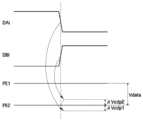
도 2는 도 1의 표시 패널을 구성하는 한 화소를 나타내는 등가 회로도이다. 도 3은 제1 및 제2 데이터선에 인가되는 데이터 전압의 극성에 따른 제1 및 제2 부화소 전극의 전압 변화를 설명하는 도면이다.2 is an equivalent circuit diagram showing one pixel constituting the display panel of FIG. 3 is a view for explaining a voltage change of the first and second sub-pixel electrodes according to polarities of data voltages applied to the first and second data lines.
도 2 및 도 3을 참고하면, 본 발명의 실시예들에 따른 표시 패널은 게이트 전압을 전달하는 게이트선(Gj)과, 게이트선(Gj)에 교차하여 형성되며 데이터 전압을 전달하는 제1 및 제2 데이터선(DAi, DBi)을 포함한다. 그리고, 게이트선(Gj)과 제1 및 제2 데이터선(DAi, DBi)에 의해 정의되는 화소(PX)는 서로 맞물려 수평 전계를 형성하는 제1 및 제2 부화소 전극(PE1, PE2)으로 이루어진다.2 and 3, a display panel according to embodiments of the present invention includes a gate line Gj for transferring a gate voltage, a first and a second gate line Gj formed to cross the gate line Gj, And second data lines DAi and DBi. The pixel PX defined by the gate line Gj and the first and second data lines DAi and DBi is connected to the first and second sub-pixel electrodes PE1 and PE2 which form a horizontal electric field .
구체적으로, 화소(PX)는 제1 및 제2 스위칭 소자(T1, T2), 제1 및 제2 부화소 전극(PE1, PE2), 액정 커패시터(Clc), 제1 및 제2 스토리지 커패시터(Cst1, Cst2)를 포함한다. 제1 및 제2 스위칭 소자(T1, T2)에 의해 액정 커패시터(Clc)의 양단에 데이터 전압이 제공됨으로써 액정 커패시터(Clc)에 화소 전압이 충전된다.Specifically, the pixel PX includes first and second switching elements T1 and T2, first and second sub-pixel electrodes PE1 and PE2, a liquid crystal capacitor Clc, first and second storage capacitors Cst1 and Cst2, , Cst2). The liquid crystal capacitor Clc is charged with the pixel voltage by providing the data voltage at both ends of the liquid crystal capacitor Clc by the first and second switching elements T1 and T2.
구체적으로, 게이트선(Gj)과 제1 데이터선(DAi)이 교차하는 지점에 제1 스위칭 소자(T1)가 형성되고, 게이트선(Gj)과 제2 데이터선(DBi)이 교차하는 지점에 제2 스위칭 소자(T2)가 형성된다. 여기서 제1 스위칭 소자(T1), 제2 스위칭 소자(T2)는 박막 트랜지스터로 이루어질 수 있다.Specifically, the first switching element T1 is formed at a position where the gate line Gj intersects with the first data line DAi, and the first switching element T1 is formed at the intersection of the gate line Gj and the second data line DBi The second switching element T2 is formed. Here, the first switching device T1 and the second switching device T2 may be formed of thin film transistors.
제1 스위칭 소자(T1)는 게이트선(Gj)에 접속된 제어 단자와, 제1 데이터선(DAi)에 접속된 입력 단자와, 액정 커패시터(Clc)의 일측에 접속된 출력 단자를 포함한다. 또한 제1 스위칭 소자(T1)의 출력 단자는 제1 부화소 전극(PE1)과 연결되며, 제1 스위칭 소자(T1)의 출력 단자와 스토리지선(SL) 사이에는 제1 스토리지 커패시터(Cst1)가 형성된다.The first switching device T1 includes a control terminal connected to the gate line Gj, an input terminal connected to the first data line DAi and an output terminal connected to one side of the liquid crystal capacitor Clc. The output terminal of the first switching element T1 is connected to the first sub-pixel electrode PE1 and a first storage capacitor Cst1 is connected between the output terminal of the first switching element T1 and the storage line SL .
유사하게, 제2 스위칭 소자(T2)는 게이트선(Gj)에 접속된 제어 단자와, 제2 데이터선(DBi)에 접속된 입력 단자와, 액정 커패시터(Clc)의 타측에 접속된 출력 단자를 포함한다. 또한, 제2 스위칭 소자(T2)의 출력 단자는 제2 부화소 전극(PE2)과 연결되며, 제2 스위칭 소자(T2)의 출력 단자와 스토리지선(SL) 사이에는 제2 스토리지 커패시터(Cst2)가 형성된다.Similarly, the second switching element T2 has a control terminal connected to the gate line Gj, an input terminal connected to the second data line DBi, and an output terminal connected to the other side of the liquid crystal capacitor Clc . The output terminal of the second switching element T2 is connected to the second sub-pixel electrode PE2 and the second storage capacitor Cst2 is connected between the output terminal of the second switching element T2 and the storage line SL. .
여기서 액정층에 포함된 액정 물질은 액정 커패시터(Clc)의 유전체로서 작용한다. 또한, 제1 스토리지 커패시터(Cst1)는 제1 스위칭 소자(T1)의 출력 단자(즉, 제1 부화소 전극(PE1)), 하부 표시판에 형성된 스토리지선(SL) 및 이들 사이에 개재된 유전 물질로 이루어지며, 제2 스토리지 커패시터(Cst2)는 제2 스위칭 소 자(T2)의 출력 단자(즉, 제2 부화소 전극(PE2)), 하부 표시판에 형성된 스토리지선(SL), 및 이들 사이에 개재된 유전 물질로 이루어진다.Here, the liquid crystal material included in the liquid crystal layer functions as a dielectric of the liquid crystal capacitor Clc. The first storage capacitor Cst1 is connected to the output terminal of the first switching device T1 (i.e., the first sub-pixel electrode PE1), the storage line SL formed in the lower panel, And the second storage capacitor Cst2 is connected to the output terminal (i.e., the second sub-pixel electrode PE2) of the second switching element T2, the storage line SL formed in the lower panel, Intervening dielectric material.
특히, 본 발명의 실시예들에 따른 표시 패널에서 제1 데이터선(DAi)과 제2 부화소 전극(PE2) 사이에는 제1 기생 커패시터(Cdp1)가 존재하는 반면, 제1 데이터선(DAi)과 제1 부화소 전극(PE1) 사이에는 기생 커패시터가 존재하지 않거나 설령 존재하더라도 그 커패시턴스가 매우 작을 수 있다. 또한, 제2 데이터선(DBi)과 제2 부화소 전극(PE2) 사이에는 제2 기생 커패시터(Cdp2)가 존재하는 반면, 제2 데이터선(DBi)과 제1 부화소 전극(PE1) 사이에는 기생 커패시터가 존재하지 않거나 설령 존재하더라도 그 커패시턴스가 매우 작을 수 있다.Particularly, in the display panel according to the embodiments of the present invention, the first parasitic capacitor Cdp1 exists between the first data line DAi and the second sub-pixel electrode PE2, while the first parasitic capacitor Cdp1 exists between the first data line DAi and the second sub- And the first sub-pixel electrode PE1, parasitic capacitors do not exist, or even if they exist, the capacitance may be very small. A second parasitic capacitor Cdp2 is present between the second data line DBi and the second sub-pixel electrode PE2 while a second parasitic capacitor Cdp2 is provided between the second data line DBi and the first sub- The parasitic capacitor may be absent or even present if its capacitance is very small.
여기서, 제1 기생 커패시터(Cdp1)는 제2 부화소 전극(PE2), 제1 데이터선(DAi) 및 이들 사이에 개재된 유전 물질로 이루어지는 반면, 제2 기생 커패시터(Cdp2)는 제2 부화소 전극(PE2), 제2 데이터선(DBi) 및 이들 사이에 개재된 유전 물질로 이루어질 수 있다.Here, the first parasitic capacitor Cdp1 is formed of the second sub-pixel electrode PE2, the first data line DAi, and a dielectric material interposed therebetween, while the second parasitic capacitor Cdp2 is formed of the second sub- An electrode PE2, a second data line DBi, and a dielectric material interposed therebetween.
제1 기생 커패시터(Cdp1)는 제1 데이터선(DAi)에 인가되는 전압이 변하는 경우, 구체적으로 제1 및 제2 스위칭 소자(T1, T2)가 오프되고 제1 데이터선(DAi)에 인가되는 제1 데이터 전압의 극성이 변하는 경우, 커플링(coupling) 현상에 의해 제2 부화소 전극(PE2)에 충전된 데이터 전압(또는 전하량)을 변화시킬 수 있다. 예를 들어, 제1 데이터선(DAi)에 인가되는 제1 데이터 전압이 정극성에서 부극성으로 변하는 경우 제2 부화소 전극(PE2)에 충전된 데이터 전압은 낮아질 수 있으며, 제1 데이터 전압이 부극성에서 정극성으로 변하는 경우 제2 부화소 전극(PE2)에 충전된 데이터 전압은 높아질 수 있다.The first parasitic capacitor Cdp1 is turned on when the voltage applied to the first data line DAi changes and specifically when the first and second switching elements T1 and T2 are turned off and applied to the first data line DAi When the polarity of the first data voltage changes, the data voltage (or charge amount) charged in the second sub-pixel electrode PE2 can be changed by a coupling phenomenon. For example, when the first data voltage applied to the first data line DAi changes from the positive polarity to the negative polarity, the data voltage charged in the second sub-pixel electrode PE2 may be lowered, The data voltage charged in the second sub-pixel electrode PE2 can be increased when the polarity changes from negative to positive.
여기서, 제1 데이터선(DAi)에 인가되는 제1 데이터 전압의 변화량을 ΔV1이라고 하고, 제1 기생 커패시터(Cdp1) 및 제1 스토리지 커패시터(Cst1)의 커패시턴스 각각 Ccdp1, Ccst1라고 할 경우, 제1 데이터선(DAi)에 의한 제2 부화소 전극(PE2)의 전압 변화량(ΔVcdp1)은 하기 수학식 1과 같다.Assuming that the amount of change of the first data voltage applied to the first data line DAi is DELTA V1 and the capacitances of the first parasitic capacitor Cdp1 and the first storage capacitor Cst1 are Ccdp1 and Ccst1, The voltage change amount? Vcdp1 of the second sub-pixel electrode PE2 by the data line DAi is given by the following equation (1).

반면, 제2 기생 커패시터(Cdp2)는 제2 데이터선(DBi)의 전압이 변하는 경우, 구체적으로, 제1 및 제2 스위칭 소자(T1, T2)가 오프되고 제2 데이터선(DBi)에 인가되는 제2 데이터 전압의 극성이 변하는 경우, 커플링 현상에 의해 제2 부화소 전극(PE2)에 충전된 데이터 전압을 변화시킬 수 있다. 예를 들어, 제2 데이터선(DBi)에 인가되는 제2 데이터 전압이 부극성에서 정극성으로 변하는 경우 제2 부화소 전극(PE2)에 충전된 데이터 전압은 높아질 수 있으며, 제2 데이터 전압이 정극성에서 부극성으로 변하는 경우 제2 부화소 전극(PE2)에 충전된 데이터 전압은 낮아질 수 있다.On the other hand, when the voltage of the second data line DBi is changed, the second parasitic capacitor Cdp2 is turned on and off by the first and second switching elements T1 and T2 and applied to the second data line DBi The data voltage charged in the second sub-pixel electrode PE2 can be changed by the coupling phenomenon. For example, when the second data voltage applied to the second data line DBi changes from negative to positive, the data voltage charged in the second sub-pixel electrode PE2 may be high, The data voltage charged in the second sub-pixel electrode PE2 may be lowered when the polarity is changed from the positive polarity to the negative polarity.
여기서, 제2 데이터선(DBi)에 인가되는 제2 데이터 전압의 변화량을 ΔV2이라고 하고, 제2 기생 커패시터(Cdp2) 및 제2 스토리지 커패시터(Cst2)의 커패시턴스 각각 Ccdp2, Ccst2라고 할 경우, 제2 데이터선(DBi)에 의한 제2 부화소 전극(PE2)의 전압 변화량(ΔVcdp2)은 하기 수학식 2와 같다.Here, when the change amount of the second data voltage applied to the second data line DBi is DELTA V2 and the capacitances of the second parasitic capacitor Cdp2 and the second storage capacitor Cst2 are respectively Ccdp2 and Ccst2, The voltage change amount? Vcdp2 of the second sub-pixel electrode PE2 by the data line DBi is given by the following equation (2).

따라서, 제1 및 제2 데이터선(DAi, DBi)에 인가되는 데이터 전압이 달라짐에 따라 제1 및 제2 기생 커패시터(Cdp1, Cdp2)에 의한 제2 부화소 전극(PE2)의 전압 변화량(ΔV)을 정리하면 하기 수학식 3과 같다.Therefore, as the data voltages applied to the first and second data lines DAi and DBi are changed, the voltage change amount? V of the second sub-pixel electrode PE2 due to the first and second parasitic capacitors Cdp1 and Cdp2 ) Is summarized as the following equation (3).

수학식 3에서 제1 및 제2 스토리지 커패시터(Cst1, Cst2)의 커패시턴스가 일정할 경우, 제2 부화소 전극(PE2)의 전압 변화량(ΔV)은 제1 및 제2 기생 커패시터(Cdp1, Cdp2)의 커패시턴스와 제1 및 제2 데이터선(DAi, DBi)에 각각 인가되는 제1 및 제2 데이터 전압의 변화량(ΔV1, ΔV2)에 따라 변할 수 있다. 그런데, 본 발명의 실시예들에서 제1 및 제2 데이터선(DAi, DBi)에 각각 인가되는 제1 및 제2 데이터 전압은 극성만 다를뿐, 각 데이터 전압의 절대값은 동일할 수 있다. 즉, 제1 데이터선(DAi)에 인가되는 제1 데이터 전압의 극성이 변함에 따른 제1 데이터 전압의 변화량(ΔV1)은 제2 데이터선(DBi)에 인가되는 제2 데이터 전압의 극성이 변함에 따른 제2 데이터 전압의 변화량(ΔV2)과 동일할 수 있다. 뿐만 아니라, 본 발명의 실시예들에서 제1 데이터선(DAi)과 제2 부화소 전극(PE2) 사이의 제1 기생 커패시터(Cdp1)의 커패시턴스는 제2 데이터선(DBi)과 제2 부화소 전극(PE2) 사이의 제2 기생 커패시터(Cdp2)의 커패시턴스와 실질적으로 동일할 수 있다.The voltage change amount? V of the second sub-pixel electrode PE2 is smaller than the voltage variation? V of the first and second parasitic capacitors Cdp1 and Cdp2 when the capacitances of the first and second storage capacitors Cst1 and Cst2 are constant, V2 of the first and second data voltages applied to the first and second data lines DAi and DBi, respectively. However, in the embodiments of the present invention, the first and second data voltages applied to the first and second data lines DAi and DBi have different polarities only, and the absolute values of the data voltages may be the same. That is, the change amount? V1 of the first data voltage according to the change of the polarity of the first data voltage applied to the first data line DAi changes according to the polarity of the second data voltage applied to the second data line DBi V2 " of the second data voltage in accordance with the first data voltage. The capacitance of the first parasitic capacitor Cdp1 between the first data line DAi and the second subpixel electrode PE2 in the embodiments of the present invention is larger than the capacitance of the second data line DBi and the second sub- May be substantially equal to the capacitance of the second parasitic capacitor Cdp2 between the electrodes PE2.
이에 의해, 제1 데이터선(DAi)과 제2 부화소 전극(PE2) 사이의 제1 기생 커패시터(Cdp1)에 의한 제2 부화소 전극(PE2)의 전압 변화량(ΔVcdp1)은 제2 데이터선(DBi)과 제2 부화소 전극(PE2) 사이의 제2 기생 커패시터(Cdp2)에 의한 제2 부화소 전극(PE2)의 전압 변화량(ΔVcdp2)과 극성만 다를뿐 실질적으로 동일할 수 있다. 따라서, 본 발명의 실시예들에서 제1 및 제2 데이터선(DAi, DBi)에 인가되는 제1 및 제2 데이터 전압의 극성이 변하더라도, 제2 부화소 전극(PE2)의 데이터 전압은 실질적으로 변하지 않을 수 있다.Thereby, the voltage change amount? Vcdp1 of the second sub-pixel electrode PE2 due to the first parasitic capacitor Cdp1 between the first data line DAi and the second sub-pixel electrode PE2 becomes the second data line Vcdp2 of the second sub-pixel electrode PE2 due to the second parasitic capacitor Cdp2 between the first sub-pixel electrode DBi and the second sub-pixel electrode PE2. Therefore, even if the polarities of the first and second data voltages applied to the first and second data lines DAi and DBi are changed in the embodiments of the present invention, the data voltage of the second sub-pixel electrode PE2 is substantially . ≪ / RTI >
또한, 제1 부화소 전극(PE1)과 제1 및 제2 데이터선(DAi, DBi) 사이에는 기생 커패시터가 존재하지 않거나, 설령 존재하더라도 그 커패시턴스가 매우 작으므로, 제1 및 제2 데이터선(DAi, DBi)에 인가되는 제1 및 제2 데이터 전압()의 극성이 변하더라도, 제1 부화소 전극(PE1)의 데이터 전압은 실질적으로 변하지 않을 수 있다.In addition, since no parasitic capacitor exists between the first sub-pixel electrode PE1 and the first and second data lines DAi and DBi or even if the parasitic capacitor is present, the first and second data lines The data voltages of the first sub-pixel electrode PE1 may not substantially change even if the polarities of the first and second data voltages applied to the data lines DAi and DBi are changed.
따라서, 본 발명의 실시예들에 따른 표시 패널은 제1 및 제2 데이터선(DAi, DBi)에 인가되는 데이터 전압의 극성이 변하더라도, 제1 및 제2 부화소 전극(PE1, PE2) 사이에 충전된 화소 전압(Vdata)이 실질적으로 변하지 않을 수 있다.Therefore, even if the polarity of the data voltage applied to the first and second data lines DAi and DBi is changed, the display panel according to the embodiments of the present invention can prevent the data voltage between the first and second sub- The charged pixel voltage Vdata may not substantially change.
도 3을 참조하여 구체적으로 설명하면, 게이트선(Gj)에 게이트 온 전압이 인가된 경우, 제1 및 제2 데이터선(DAi, DBi)으로부터 제1 및 제2 부화소 전극(PE1, PE2)에 각각 7V, -7V의 데이터 전압이 전달될 수 있다. 즉, 제1 및 제2 부화소 전극(PE1, PE2) 사이에는 14V의 화소 전압이 인가될 수 있다.3, when the gate-on voltage is applied to the gate line Gj, the first and second sub-pixel electrodes PE1 and PE2 are turned on from the first and second data lines DAi and DBi, The data voltages of 7V and -7V can be transmitted to the data lines. That is, a pixel voltage of 14V may be applied between the first and second sub-pixel electrodes PE1 and PE2.
그리고, 게이트선(Gj)에 게이트 오프 전압이 인가되고, 표시 장치가 컬 럼(column) 반전 또는 도트(dot) 반전을 함에 따라 제1 및 제2 데이터선(DAi, DBi)에 각각 -7V, 7V의 데이터 전압이 전달되더라도 제1 및 제2 부화소 전극(PE1, PE2) 사이에 충전된 화소 전압은 실질적으로 변하지 않을 수 있다. 구체적으로, 제1 부화소 전극(PE1)과 제1 및 제2 데이터선(DAi, DBi) 사이에는 별도의 기생 커패시터가 존재하지 않거나 설령 존재하더라도 그 커패시턴스가 매우 작으므로, 제1 및 제2 데이터선(DAi, DBi)에 인가된 데이터 전압에 의해 제1 부화소 전극(PE1)이 영향을 받지 않을 수 있다.When a gate off voltage is applied to the gate line Gj and the display device performs a column inversion or a dot inversion operation, a voltage of -7 V is applied to the first and second data lines DAi and DBi, The charged pixel voltage between the first and second sub-pixel electrodes PE1 and PE2 may not substantially change even if a data voltage of 7V is transmitted. More specifically, since a parasitic capacitor does not exist or is present between the first sub-pixel electrode PE1 and the first and second data lines DAi and DBi, the capacitance of the parasitic capacitor is very small, The first sub-pixel electrode PE1 may not be affected by the data voltage applied to the lines DAi and DBi.
또한, 제2 부화소 전극(PE2)과 제1 및 제2 데이터선(DAi, DBi) 사이에는 제1 및 제2 기생 커패시터(Cdp1, Cdp2)가 존재할지라도 앞에서 설명한 바와 같이, 제1 기생 커패시터(Cdp1)에 의한 제2 부화소 전극(PE2)의 전압 변화량(ΔVcdp1)과 제2 기생 커패시터(Cdp2)에 의한 제2 부화소 전극(PE2)의 전압 변화량(ΔVcdp2)은 극성만 다를뿐 실질적으로 동일할 수 있다. 즉, 제1 및 제2 데이터선(DAi, DBi)에 인가된 데이터 전압에 의해 제2 부화소 전극(PE2)이 실질적으로 영향을 받지 않을 수 있다.Although the first and second parasitic capacitors Cdp1 and Cdp2 exist between the second sub-pixel electrode PE2 and the first and second data lines DAi and DBi, as described above, the first parasitic capacitor The voltage change amount? Vcdp1 of the second sub-pixel electrode PE2 by the first parasitic capacitor Cdp1 and the voltage change amount? Vcdp2 of the second sub-pixel electrode PE2 by the second parasitic capacitor Cdp2 are substantially the same can do. That is, the second sub-pixel electrode PE2 may not be substantially affected by the data voltage applied to the first and second data lines DAi and DBi.
따라서, 본 발명의 실시예들에 따른 표시 패널은 제1 및 제2 스위칭 소자(T1, T2)가 오프된 이후, 제1 및 제2 데이터선(DAi, DBi)에 인가되는 데이터 전압의 극성이 변하더라도 제1 및 제2 부화소 전극(PE1, PE2) 사이에 충전된 화소 전압이 실질적으로 변하지 않으므로, 화질이 향상될 수 있다.Therefore, after the first and second switching elements T1 and T2 are turned off, the polarity of the data voltage applied to the first and second data lines DAi and DBi becomes The pixel voltage charged between the first and second sub-pixel electrodes PE1 and PE2 does not substantially change, so that the image quality can be improved.
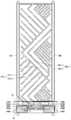
이하 도 4 내지 도 7을 참조하여 본 발명의 일 실시예에 따른 표시 패널을 설명한다. 도 4는 본 발명의 일 실시예에 따른 표시 패널의 하부 표시판의 배치도 이다. 도 5은 도 4의 Ⅴ- Ⅴ'을 따라 절단된 단면도이다. 도 6a는 제1 및 제2 데이터선과 제1 부화소 전극의 배치를 구체적으로 설명하는 도면이며, 도 6b 제1 및 제2 데이터선과 제2 부화소 전극의 배치를 구체적으로 설명하는 도면이다. 도 7은 도 4의 변형 실시예를 설명하는 도면이다.Hereinafter, a display panel according to an embodiment of the present invention will be described with reference to FIGS. 4 is a layout view of a lower panel of a display panel according to an embodiment of the present invention. 5 is a cross-sectional view taken along line V-V 'of FIG. FIG. 6A is a view for explaining the arrangement of the first and second data lines and the first sub-pixel electrode, and FIG. 6B is a view for specifically explaining the arrangement of the first and second data lines and the second sub-pixel electrode. 7 is a view for explaining a modified embodiment of Fig.
본 실시예에 따른 표시 패널은 박막 트랜지스터 어레이(thin film transistor array)가 형성된 하부 표시판, 이에 대향하는 상부 표시판, 및 이들 사이에 개재된 액정층을 포함한다.The display panel according to the present embodiment includes a lower display panel on which a thin film transistor array is formed, an upper display panel facing thereto, and a liquid crystal layer interposed therebetween.
먼저 도 4 및 도 5를 참조하여 하부 표시판을 설명하면, 투명한 유리 등으로 이루어진 절연 기판(510) 위에 주로 가로 방향으로 뻗어 있고 게이트 신호를 전달하는 게이트선(Gj)이 형성되어 있다. 게이트선(Gj)은 하나의 화소에 대하여 하나씩 할당되어 있다. 그리고, 게이트선(Gj)에는 돌출한 제1 및 제2 게이트 전극(540a, 540b)이 형성되어 있다. 제1 게이트 전극(540a)은 제1 데이터선(DAi)과의 교차 영역에 형성되고, 제2 게이트 전극(540b)은 제2 데이터선(DBi)과의 교차 영역에 형성된다. 이러한 게이트선(Gj)과 제1 및 제2 게이트 전극(540a, 540b)을 게이트 배선이라 한다.4 and 5, a gate line Gj extending in a lateral direction and transmitting a gate signal is formed on an insulating
또한 절연 기판 위에는 화소 영역을 가로질러 게이트선(Gj)과 실질적으로 평행하게 가로 방향으로 뻗어 있는 스토리지선(storage line)(SL)이 형성되어 있다. 스토리지선(SL)은 제1 및 제2 부화소 전극(610_1, 620_1)과 중첩되어 화소의 전하 보존 능력을 향상시키는 스토리지 커패시터(storage capacitor)를 형성한다. 여기서, 스토리지선(SL)의 모양 및 배치는 여러 형태로 변형될 수 있다.On the insulating substrate, a storage line SL extending in the horizontal direction substantially parallel to the gate line Gj is formed across the pixel region. The storage line SL overlaps with the first and second sub-pixel electrodes 610_1 and 620_1 to form a storage capacitor for improving the charge storage ability of the pixel. Here, the shape and arrangement of the storage line SL can be modified into various forms.
게이트 배선과 스토리지선(SL)은 알루미늄(Al)과 알루미늄 합금 등 알루미늄 계열의 금속, 은(Ag)과 은 합금 등 은 계열의 금속, 구리(Cu)와 구리 합금 등 구리 계열의 금속, 몰리브덴(Mo)과 몰리브덴 합금 등 몰리브덴 계열의 금속, 크롬(Cr), 티타늄(Ti), 탄탈륨(Ta) 따위로 이루어질 수 있다. 또한, 게이트 배선과 스토리지선(SL)은 물리적 성질이 다른 두 개의 도전막(도시하지 않음)을 포함하는 다중막 구조를 가질 수도 있다. 이 중 한 도전막은 게이트 배선과 스토리지선(SL)의 신호 지연이나 전압 강하를 줄일 수 있도록 낮은 비저항(resistivity)의 금속, 예를 들면 알루미늄 계열 금속, 은 계열 금속, 구리 계열 금속 등으로 이루어진다. 이와는 달리, 다른 도전막은 다른 물질, 특히 ITO(Indium Tin Oxide) 및 IZO(Indium Zinc Oxide)와의 접촉 특성이 우수한 물질, 이를테면 몰리브덴 계열 금속, 크롬, 티타늄, 탄탈륨 등으로 이루어진다. 이러한 조합의 좋은 예로는 크롬 하부막과 알루미늄 상부막 및 알루미늄 하부막과 몰리브덴 상부막을 들 수 있다. 다만, 본 발명은 이에 한정되지 않으며, 게이트 배선과 스토리지선(SL)은 다양한 여러 가지 금속과 도전체로 만들어질 수 있다.The gate wiring and the storage line (SL) are made of aluminum metal such as aluminum (Al) and aluminum alloy, metal of series metal such as silver (Ag) and silver alloy, copper metal such as copper and copper alloy, molybdenum Mo, and a molybdenum alloy, such as a molybdenum metal, chromium (Cr), titanium (Ti), and tantalum (Ta). Further, the gate wiring and the storage line SL may have a multi-film structure including two conductive films (not shown) having different physical properties. One of the conductive films is made of a metal having a low resistivity, for example, an aluminum-based metal, a silver-based metal, a copper-based metal, or the like so as to reduce signal delays and voltage drop of the gate wiring and the storage line (SL). Alternatively, the other conductive film is made of a material having excellent contact properties with other materials, particularly ITO (Indium Tin Oxide) and IZO (Indium Zinc Oxide), such as molybdenum metal, chromium, titanium, tantalum and the like. A good example of such a combination is a chromium bottom film, an aluminum top film, an aluminum bottom film and a molybdenum top film. However, the present invention is not limited thereto, and the gate wiring and the storage line SL can be made of various metals and conductors.
게이트선(Gj) 및 스토리지선(SL) 위에는 질화규소(SiNx) 등으로 이루어진 게이트 절연막(530)이 형성되어 있다.A
게이트 절연막(530) 위에는 수소화 비정질 규소(hydrogenated amorphous silicon) 또는 다결정 규소 등으로 이루어진 제1 및 제2 반도체층(540a, 540b)이 형성되어 있다. 제1 반도체층(540a)은 제1 게이트 전극(540a)과 중첩되고, 제2 반도체층(540b)은 제2 게이트 전극(540b)과 중첩된다. 각 반도체층(540a, 540b)은 섬 형(island shape), 선형(line shape) 등과 같이 다양한 형상을 가질 수 있으며, 예를 들어 본 실시예에서와 같이 섬형으로 형성될 수 있다.First and
각 반도체층(540a, 540b)의 상부에는 실리사이드(silicide) 또는 n형 불순물이 고농도로 도핑되어 있는 n+ 수소화 비정질 규소 등의 물질로 만들어진 오믹 콘택층(ohmic contact layer)(예, 555a, 556a)이 형성되어 있다. 오믹 콘택층(555a, 556a)은 쌍(pair)을 이루어 반도체층(예, 640a) 위에 위치한다.An
오믹 콘택층(555a, 556a) 및 게이트 절연막(530) 위에는 한 쌍의 제1 및 제2 데이터선(DAi, DBi), 상기 제1 데이터선(DAi)에 대응하는 제1 드레인 전극(566a)과 상기 제2 데이터선(DBi)에 대응하는 제2 드레인 전극(566b)이 형성되어 있다.A pair of first and second data lines DAi and DBi and a
제1 및 제2 데이터선(DAi, DBi)은 주로 세로 방향으로 뻗어 게이트선(Gj) 및 스토리지선(SL)과 교차하며 데이터 전압을 전달한다. 제1 데이터선(DAi)에는 제1 드레인 전극(566a)을 향하여 각각 뻗은 제1 소스 전극(565a)이 형성되어 있다. 제2 데이터선(DBi)에는 제2 드레인 전극(566b)을 향하여 각각 뻗은 제2 소스 전극(565b)이 형성되어 있다. 도 4에 도시된 바와 같이, 하나의 화소가 제1 및 제2 부화소 전극(610_1, 620_1)으로 구성되는 경우, 제1 및 제2 데이터선(DAi, DBi)은 제1 및 제2 부화소 전극(610_1, 620_1)에 각각 극성이 다른 데이터 전압을 전달한다. 구체적으로, 제1 및 제2 데이터선(DAi, DBi)은 제1 및 제2 부화소 전극(610_1, 620_1)에 서로 절대값은 동일하나 극성이 다른 제1 및 제2 데이터 전압을 각각 전달할 수 있다.The first and second data lines DAi and DBi extend mainly in the longitudinal direction and intersect the gate line Gj and the storage line SL to transfer the data voltage. A
이러한 제1 및 제2 데이터선(DAi, DBi), 제1 및 제2 소스 전극(565a, 565b), 제1 및 제2 드레인 전극(566a, 566b)을 데이터 배선이라고 한다.The first and second data lines DAi and DBi, the first and
데이터 배선은 크롬, 몰리브덴 계열의 금속, 탄탈륨 및 티타늄 등 내화성 금속으로 이루어지는 것이 바람직하며, 내화성 금속 따위의 하부막(미도시)과 그 위에 위치한 저저항 물질 상부막(미도시)으로 이루어진 다층막 구조를 가질 수 있다. 다층막 구조의 예로는 앞서 설명한 크롬 하부막과 알루미늄 상부막 또는 알루미늄 하부막과 몰리브덴 상부막의 이중막 외에도 몰리브덴막-알루미늄막-몰리브덴막의 삼중막을 들 수 있다.The data wiring is preferably made of a refractory metal such as chromium, molybdenum series metal, tantalum and titanium, and a multi-layer structure composed of a lower film (not shown) such as refractory metal and a low resistance material upper film Lt; / RTI > Examples of the multilayer structure include a triple layer of a molybdenum film-aluminum film-molybdenum film in addition to the chromium lower film and the aluminum upper film or the aluminum lower film and the molybdenum upper film.
제1 및 제2 소스 전극(565a, 565b)은 각각 반도체층(540a, 540b)과 적어도 일부분이 중첩되고, 제1 및 제2 드레인 전극(566a, 566b)은 각각 게이트 전극(526a, 526b)을 중심으로 제1 및 제2 소스 전극(565a, 565b)과 대향하며 반도체층(540a, 540b)과 적어도 일부분이 중첩된다. 여기서, 앞서 언급한 오믹 콘택층은 그 하부의 반도체층(540a, 540b)과, 그 상부의 제1 및 제2 소스 전극(565a, 565b)과 제1 및 제2 드레인 전극(566a, 566b) 사이에 존재하며 접촉 저항을 낮추어 주는 역할을 한다.The first and
데이터 배선과 노출된 반도체층(540a, 540b) 위에는 보호막(passivation layer)(570)이 형성되어 있다. 보호막(570)은 질화규소 또는 산화규소로 이루어진 무기물, 평탄화 특성이 우수하며 감광성(photosensitivity)을 가지는 유기물 또는 플라스마 화학 기상 증착(plasma enhanced chemical vapor deposition, PECVD)으로 형성되는 a-Si:C:O, a-Si:O:F 등의 저유전율 절연 물질 등으로 이루어진다. 또한, 보호막(570)은 유기막의 우수한 특성을 살리면서도 노출된 반도체층(540a, 540b) 부분을 보호하기 위하여 하부 무기막과 상부 유기막의 이중막 구조를 가질 수 있다. 나아가 보호막으로는 적색, 녹색 또는 청색의 컬러필터층이 사용될 수도 있다.A
보호막(570) 상에는 제1 및 제2 콘택홀(576a, 576b)을 통하여 각각 제1 및 제2 드레인 전극(566a, 566b)과 전기적으로 연결된 제1 및 제2 부화소 전극(610_1, 620_1)이 형성되어 있다. 여기서, 제1 및 제2 부화소 전극(610_1, 620_1)은 ITO 또는 IZO 따위의 투명 도전체 또는 알루미늄 따위의 반사성 도전체로 이루어진다. 이러한 제1 및 제2 부화소 전극(610_1, 620_1)은 한 화소에 대한 화소 전극을 구성한다.First and second sub-pixel electrodes 610_1 and 620_1, which are electrically connected to the first and
한편 도 2 및 도 4를 참조하면, 액정 커패시터(Clc)는 제1 부화소 전극(610_1)과 제2 부화소 전극(620_1)을 양 단자로 하고, 제1 및 제2 스위칭 소자(T1, T2)가 턴 오프된 후에도 액정 커패시터(Clc1)의 전하 보존 능력을 향상시키기 위하여 제1 및 제2 스토리지 커패시터(Cst1, Cst2)가 형성될 수 있다. 이 때, 제1 스토리지 커패시터(Cst1)는 스토리지선(SL)을 제1 부화소 전극(610_1) 또는 이에 연결되어 있는 제1 드레인 전극(566a)에 중첩시킴으로써 형성되고, 제2 스토리지 커패시터(Cst2)는 스토리지선(SL)을 제2 부화소 전극(620_1) 또는 이에 연결되어 있는 제2 드레인 전극(566b)에 중첩시킴으로써 형성될 수 있다.2 and 4, the liquid crystal capacitor Clc includes a first sub-pixel electrode 610_1 and a second sub-pixel electrode 620_1 as both terminals, and the first and second switching elements T1 and T2 The first and second storage capacitors Cst1 and Cst2 may be formed to improve the charge storage capability of the liquid crystal capacitor Clc1 even after the first and second storage capacitors Clc1 and Clc2 are turned off. The first storage capacitor Cst1 is formed by overlapping the storage line SL with the first sub-pixel electrode 610_1 or the
제1 및 제2 부화소 전극(610_1, 620_1)은 각각 제1 및 제2 콘택홀(576a, 576b)을 통하여 제1 및 제2 드레인 전극(566a, 566b)과 물리적·전기적으로 연결되어 제1 및 제2 드레인 전극(566a, 566b)으로부터 데이터 전압을 인가 받는다. 제1 부화소 전극(610_1)에는 제1 데이터선(DAi)으로부터 제1 데이터 전압이 인가되고, 제2 부화소 전극(620_1)에는 제2 데이터선(DBi)으로부터 제2 데이터 전압이 인가된다.The first and second sub-pixel electrodes 610_1 and 620_1 are physically and electrically connected to the first and
제1 데이터 전압이 인가된 제1 부화소 전극(610_1)과 제2 데이터 전압이 인가된 제2 부화소 전극(620_1) 사이에 수평 전계가 형성되어, 제1 및 제2 부화소 전극(610_1, 620_1) 상부에 위치하는 액정 분자들의 배열이 결정된다. 이러한 제1 부화소 전극(610_1)은 소정의 방향으로 나란히 뻗은 제1 스트라이프(611_1)와 이를 연결하는 제1 연결부(612_1)로 이루어져 있고, 제2 부화소 전극(620_1)은 제1 스트라이프(611_1)와 평행한 제2 스트라이프(621_1)와 이를 연결하는 제2 연결부(622_1)로 이루어져 있다. 즉, 제1 부화소 전극(610_1) 및 제2 부화소 전극(620_1)은 소정의 간극(gap)을 사이에 두고 서로 맞물려 있으며 서로 전기적으로 분리될 수 있다.A horizontal electric field is formed between the first sub-pixel electrode 610_1 to which the first data voltage is applied and the second sub-pixel electrode 620_1 to which the second data voltage is applied, so that the first and second sub-pixel electrodes 610_1, 620_1) is determined. The first sub-pixel electrode 610_1 includes a first stripe 611_1 extending in a predetermined direction and a first connection portion 612_1 connecting the first stripe 611_1 and the first stripe 611_1. The second sub-pixel electrode 620_1 includes a first stripe 611_1, And a second connection part 622_1 connecting the second stripe 621_1 and the second stripe 621_1. That is, the first sub-pixel electrode 610_1 and the second sub-pixel electrode 620_1 are interdigitated with each other with a predetermined gap therebetween and can be electrically separated from each other.
특히, 본 발명의 일 실시예에서 제2 부화소 전극(620_1)은 제1 및 제2 데이터선(DAi, DBi)과 제1 및 제2 데이터선(DAi, DBi)을 따라 중첩된다. 구체적으로, 제2 부화소 전극(620_1)은 제2 데이터선(DBi), 전단 게이트선(미도시) 및 제1 데이터선(DAi)을 따라 형성되어, 도 6a에 도시된 바와 같이 제1 및 제2 데이터선(DAi, DBi)과 중첩될 수 있다.Particularly, in an embodiment of the present invention, the second sub-pixel electrode 620_1 is overlapped with the first and second data lines DAi and DBi and the first and second data lines DAi and DBi. Specifically, the second sub-pixel electrode 620_1 is formed along the second data line DBi, the previous gate line (not shown), and the first data line DAi, Can be overlapped with the second data lines DAi and DBi.
도면에서는 제2 부화소 전극(620_1)과 제1 및 제2 데이터선(DAi, DBi)이 완전히(fully) 중첩하는 것으로 도시하였으나 이에 한정하는 것은 아니다. 예를 들어, 본 발명의 변형된 실시예에서 제2 부화소 전극(620_2)과 제1 및 제2 데이터선(DAi, DBi)은 도 7에 도시된 바와 같이 일부(partially) 중첩할 수도 있다. 도 7 의 변형된 실시예에서 제1 및 제2 부화소 전극(610_2, 620_2)은 제2 부화소(620_2)가 제1 및 제2 데이터선(DAi, DBi)과 일부 중첩한 것을 제외하고는 도 4의 제1 및 제2 부화소 전극(610_1, 620_1)과 실질적으로 동일할 수 있다.Although the second sub-pixel electrode 620_1 and the first and second data lines DAi and DBi are fully overlapped in the drawing, the present invention is not limited thereto. For example, in a modified embodiment of the present invention, the second sub-pixel electrode 620_2 and the first and second data lines DAi and DBi may partially overlap as shown in FIG. In the modified embodiment of FIG. 7, the first and second sub-pixel electrodes 610_2 and 620_2 are the same as the first and second sub-pixel electrodes 610_2 and 620_2, except that the second sub-pixel 620_2 partially overlaps the first and second data lines DAi and DBi May be substantially the same as the first and second sub-pixel electrodes 610_1 and 620_1 of FIG.
이에 의해, 제2 부화소 전극(620_1)과 제1 데이터선(DAi) 사이에는 도 2에 도시된 바와 같이 제1 기생 커패시터(Cdp1)가 존재할 수 있으며, 제2 부화소 전극(620_1)과 제2 데이터선(DBi) 사이에는 제2 기생 커패시터(Cdp2)가 존재할 수 있다.2, the first parasitic capacitor Cdp1 may exist between the second sub-pixel electrode 620_1 and the first data line DAi, and the first parasitic capacitor Cdp1 may exist between the second sub-pixel electrode 620_1 and the first data line DAi. A second parasitic capacitor Cdp2 may exist between the two data lines DBi.
여기서, 제2 부화소 전극(620_1)과 제1 데이터선(DAi) 간의 중첩 면적은 제2 부화소 전극(620_1)과 제2 데이터선(DBi) 간의 중첩 면적과 실질적으로 동일할 수 있다. 즉, 제1 기생 커패시터(Cdp1)의 커패시턴스와 제2 기생 커패시터(Cdp2)의 커패시턴스가 실질적으로 동일할 수 있도록, 제2 부화소 전극(620_1)과 제1 데이터선(DAi) 간의 중첩 면적과 제2 부화소 전극(620_1)과 제2 데이터선(DBi) 간의 중첩 면적은 실질적으로 동일할 수 있다.Here, the overlapping area between the second sub-pixel electrode 620_1 and the first data line DAi may be substantially the same as the overlapping area between the second sub-pixel electrode 620_1 and the second data line DBi. That is, the overlapping area between the second sub-pixel electrode 620_1 and the first data line DAi and the overlapping area between the second sub-pixel electrode 620_1 and the first data line DAi are set so that the capacitance of the first parasitic capacitor Cdp1 and the capacitance of the second parasitic capacitor Cdp2 may be substantially the same. The overlapping area between the second sub-pixel electrode 620_1 and the second data line DBi may be substantially the same.
반면에, 제1 부화소 전극(610_1)은 도 6b에 도시된 바와 같이 제1 및 제2 데이터선(DAi, DBi)으로부터 이격되어 형성된다. 구체적으로, 제1 부화소 전극(610_1)은 제1 및 제2 데이터선(DAi, DBi)과 중첩되어 형성된 제2 부화소 전극(620_1)으로부터 소정의 간극을 사이에 두고 형성되어, 제1 및 제2 데이터선(DAi, DBi)으로부터 이격되어 형성될 수 있다. 이에 의해, 제2 부화소 전극(620_1)과 달리 제1 부화소 전극(610_1)과 제1 및 제2 데이터선(DAi, DBi) 사이에는 기생 커패시터가 존재하지 않거나, 설령 존재하더라도 그 커패시턴스가 매우 작을 수 있다.On the other hand, the first sub-pixel electrode 610_1 is formed apart from the first and second data lines DAi and DBi as shown in FIG. 6B. Specifically, the first sub-pixel electrode 610_1 is formed with a predetermined gap therebetween from the second sub-pixel electrode 620_1 formed to overlap with the first and second data lines DAi and DBi, May be formed spaced apart from the second data lines DAi and DBi. As a result, unlike the second sub-pixel electrode 620_1, no parasitic capacitor exists between the first sub-pixel electrode 610_1 and the first and second data lines DAi and DBi, or even if the parasitic capacitor is present, Can be small.
따라서, 본 발명의 일 실시예에 따른 표시 패널은 제1 및 제2 데이터선(DAi, DBi)에 인가되는 제1 및 제2 데이터 전압의 극성이 변하더라도, 제1 및 제2 부화소 전극(610_1, 620_1)의 데이터 전압은 실질적으로 변하지 않을 수 있다. 이에 의해 본 발명의 일 실시예에 따른 표시 패널은 화질 불량이 감소된 영상을 제공할 수 있다.Therefore, even if the polarities of the first and second data voltages applied to the first and second data lines DAi and DBi are changed, the display panel according to the embodiment of the present invention can prevent the first and second sub- 610_1, and 620_1 may not substantially change. Accordingly, the display panel according to an embodiment of the present invention can provide an image with a reduced image quality defect.
뿐만 아니라, 본 발명의 일 실시예에 따른 표시 패널에서는 제1 및 제2 부화소 전극(610_1, 620_1)으로 구성되는 화소 전극(특히, 제2 부화소 전극)이 제1 및 제2 데이터선(DAi, DBi)에 중첩되어 형성되므로, 표시 패널의 개구율이 향상될 수 있다.In addition, in a display panel according to an exemplary embodiment of the present invention, a pixel electrode (particularly, a second sub-pixel electrode) including first and second sub-pixel electrodes 610_1 and 620_1 is connected to the first and second data lines DAi, and DBi, the aperture ratio of the display panel can be improved.
이와 같은 제1 및 제2 부화소 전극(610_1, 620_1)과 보호막(570) 위에는 액정층을 배향할 수 있는 배향막(미도시)이 도포될 수 있다.On the first and second sub-pixel electrodes 610_1 and 620_1 and the
이하 상부 표시판에 대하여 설명한다. 상부 표시판(미도시)은 앞서 설명한 하부 표시판과 대향하도록 배치되며, 절연기판(미도시), 블랙 매트릭스(미도시), 컬러필터(미도시) 등으로 이루어질 수 있다.Hereinafter, the upper display panel will be described. The upper panel (not shown) is disposed to face the lower panel described above, and may be formed of an insulating substrate (not shown), a black matrix (not shown), a color filter (not shown), or the like.
구체적으로, 투명한 유리 등으로 이루어진 절연 기판 위에 빛샘을 방지하고 화소 영역을 정의하는 블랙 매트릭스가 형성되어 있다. 블랙 매트릭스는 게이트선(Gj)과 제1 및 제2 데이터선(DAi, DBi)에 대응하는 부분과 스위칭 소자들에 대응하는 부분에 형성될 수 있다. 블랙 매트릭스는 크롬, 크롬 산화물 등의 금속(금속 산화물), 또는 유기 블랙 레지스트 등으로 이루어질 수 있다. 블랙 매트릭스 사이 의 화소 영역에는 적색, 녹색, 청색의 컬러필터(미도시)가 순차적으로 배열될 수 있다.Specifically, a black matrix is formed on an insulating substrate made of transparent glass or the like to prevent light leakage and define a pixel region. The black matrix may be formed at a portion corresponding to the gate line Gj, a portion corresponding to the first and second data lines DAi and DBi, and a portion corresponding to the switching elements. The black matrix may be made of a metal (metal oxide) such as chromium or chromium oxide, or an organic black resist. In the pixel region between the black matrixes, red, green, and blue color filters (not shown) may be sequentially arranged.
이러한 컬러필터 위에는 이들의 단차를 평탄화 하기 위한 오버코트층(overcoat layer)이 형성될 수 있고, 오버코트층 위에는 액정 분자들을 배향하는 배향막(미도시)이 도포될 수 있다.On the color filter, an overcoat layer may be formed to planarize the stepped portions, and an alignment layer (not shown) may be applied on the overcoat layer to align the liquid crystal molecules.
이와 같은 구조의 하부 표시판과 상부 표시판 사이에 액정층이 개재되는데, 액정층에 포함되어 있는 액정 분자는 초기 배향이 하부 표시판 및 상부 표시판에 수평한 방향으로 배향되어 있고, 양의 유전율 이방성을 가진다. 따라서 부화소 전극들 사이에서 수평 전계가 형성되는 경우 액정 분자의 장축이 이러한 전계 방향에 나란하도록 액정 분자가 배향된다.A liquid crystal layer is interposed between the lower display panel and the upper display panel having such a structure. The liquid crystal molecules included in the liquid crystal layer are oriented in a horizontal direction on the lower display panel and the upper display panel, and have a positive dielectric anisotropy. Accordingly, when a horizontal electric field is formed between the sub-pixel electrodes, the liquid crystal molecules are oriented such that the major axis of the liquid crystal molecules is aligned with the electric field direction.
도 8은 본 발명의 다른 실시예에 따른 표시 패널의 하부 표시판의 배치도이다. 설명의 편의상, 본 발명의 일 실시예의 도면(도 4 내지 도 7)에 나타낸 각 부재와 동일 기능을 갖는 부재는 동일 부호로 나타내고, 따라서 그 설명은 생략하며, 이하 차이점을 위주로 설명한다.8 is a layout view of a lower panel of a display panel according to another embodiment of the present invention. For convenience of explanation, members having the same functions as the members shown in the drawings (Figs. 4 to 7) of the embodiment of the present invention are denoted by the same reference numerals, and the description thereof will be omitted.
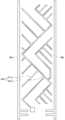
도 4 및 도 8을 참고하면, 본 발명의 다른 실시예에 따른 표시 패널은 제2 부화소 전극(620_3)과 제1 및 제2 데이터선(DAi, DBi)과 중첩하지 않는 것을 제외하고는 본 발명의 일 실시예와 실질적으로 동일할 수 있다.4 and 8, a display panel according to another embodiment of the present invention includes a first subpixel electrode 620_2 and a second subpixel electrode 620_2, except that the second subpixel electrode 620_3 and the first and second data lines DAi and DBi are not overlapped. May be substantially the same as an embodiment of the invention.
구체적으로, 본 발명의 다른 실시예에 따른 표시 패널에서 제2 부화소 전극(620_3)은 제2 데이터선(DBi), 전단 게이트선(미도시) 및 제1 데이터선(DAi)을 따라 형성되되, 제1 및 제2 데이터선(DAi, DBi)과는 중첩되지 않는다. 즉, 제2 부 화소 전극(620_3)은 도 8에 도시된 바와 같이 제1 및 제2 데이터선(DAi, DBi)에 인접하여 형성될 수 있다.In detail, the second sub-pixel electrode 620_3 in the display panel according to another embodiment of the present invention is formed along the second data line DBi, the previous gate line (not shown) and the first data line DAi , And the first and second data lines DAi and DBi. That is, the second sub-pixel electrode 620_3 may be formed adjacent to the first and second data lines DAi and DBi as shown in FIG.
여기서, 제2 부화소 전극(620_3), 제1 데이터선(DAi) 및 이들 사이에 개재된 유전 물질에 의해 제1 기생 커패시터가 형성되며, 제2 부화소 전극(620_3), 제2 데이터선(DBi) 및 이들 사이에 개재된 유전 물질에 의해 제2 기생 커패시터가 형성될 수 있다. 도 8의 실시예에서 형성된 제1 및 제2 기생 커패시터의 커패시턴스는 제2 부화소 전극(620_3)과 제1 및 제2 데이터선(DAi, DBi)이 중첩되지 않으므로, 도 4의 실시예에서의 제1 및 제2 기생 커패시터의 커패시턴스보다는 작을 수 있다.Here, a first parasitic capacitor is formed by the second sub-pixel electrode 620_3, the first data line DAi, and the dielectric material interposed therebetween, and the second sub-pixel electrode 620_3 and the second data line DBi) and a dielectric material interposed therebetween, a second parasitic capacitor can be formed. The capacitance of the first and second parasitic capacitors formed in the embodiment of FIG. 8 is different from that of the embodiment of FIG. 4 because the second sub-pixel electrode 620_3 and the first and second data lines DAi and DBi are not overlapped. May be less than the capacitance of the first and second parasitic capacitors.
또한, 제1 부화소 전극(610_3)은 제1 및 제2 데이터선(DAi, DBi)으로부터 이격되어, 제1 부화소 전극(610_3)과 제1 및 제2 데이터선(DAi, DBi) 사이에는 기생 커패시터가 존재하지 않거나 설령 존재하더라도 기생 커패시터의 커패시턴스는 매우 작을 수 있다.The first sub-pixel electrode 610_3 is spaced apart from the first and second data lines DAi and DBi and is provided between the first sub-pixel electrode 610_3 and the first and second data lines DAi and DBi The capacitance of the parasitic capacitor can be very small even if the parasitic capacitor is not present or even exists.
이에 의해, 도 8의 실시예는 도 4의 실시예와 동일하게 제1 및 제2 데이터선(DAi, DBi)에 인가되는 제1 및 제2 데이터 전압의 극성이 변하더라도, 제1 및 제2 부화소 전극(610_3, 620_3) 사이에 충전된 화소 전압은 실질적으로 변하지 않을 수 있다.8, even if the polarities of the first and second data voltages applied to the first and second data lines DAi and DBi are changed as in the embodiment of Fig. 4, the first and second The pixel voltage charged between the sub-pixel electrodes 610_3 and 620_3 may not substantially change.
도 9는 본 발명의 또 다른 실시예에 따른 표시 패널의 하부 표시판의 배치도이다. 설명의 편의상, 본 발명의 일 실시예의 도면에 나타낸 각 부재와 동일 기능을 갖는 부재는 동일 부호로 나타내고, 따라서 그 설명은 생략하며, 이하 차이점을 위주로 설명한다.9 is a layout view of a lower panel of a display panel according to another embodiment of the present invention. For convenience of explanation, members having the same functions as those of the members shown in the drawings of the embodiment of the present invention are denoted by the same reference numerals, and a description thereof will be omitted.
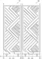
도 4 및 도 9를 참고하면, 본 발명의 또 다른 실시예에 따른 표시 패널은 제1 및 제2 데이터선(DAi, DBi)이 절곡부(562a, 562b, 563a, 563b)를 포함하는 것을 제외하고는 본 발명의 일 실시예에와 실질적으로 동일할 수 있다.4 and 9, a display panel according to another exemplary embodiment of the present invention includes a plurality of data lines DAi and DBi, except that the first and second data lines DAi and DBi include
구체적으로, 제1 및 제2 데이터선(DAi, DBi)은 세로 방향으로 뻗어 형성되지 않으며, 적어도 하나의 절곡부(562a, 562b, 563a, 563b)를 포함한다. 구체적으로, 제1 및 제2 데이터선(DAi, DBi)은 제1 방향에서 제2 방향으로 절곡되는 제1 절곡부(562a, 562b) 및 제2 방향에서 제1 방향으로 절곡되는 제2 절곡부(563a, 563b)를 포함할 수 있다.Specifically, the first and second data lines DAi and DBi are not formed in the longitudinal direction and include at least one
제1 및 제2 부화소 전극(610_4, 620_4)은 소정의 간극을 사이에 두고 서로 맞물려 있으며, 제1 및 제2 데이터선(DAi, DBi)으로부터 전달받은 데이터 전압을 이용하여 수평 전계를 형성한다. 이러한, 제1 부화소 전극(610_4)은 소정의 방향으로 나란히 뻗은 제1 스트라이프(611_4)와 이를 연결하는 제1 연결부(612_4)로 이루어져 있고, 제2 부화소 전극(620_4)은 제1 스트라이프(611_4)와 평행한 제2 스트라이프(621_4)와 이를 연결하는 제2 연결부(622_4)로 이루어져 있다.The first and second sub-pixel electrodes 610_4 and 620_4 are interdigitated with each other with a predetermined gap therebetween and form a horizontal electric field by using the data voltage received from the first and second data lines DAi and DBi . The first sub-pixel electrode 610_4 includes a first stripe 611_4 extending in a predetermined direction and a first connection portion 612_4 connecting the first stripe 611_4 and the first stripe 611_4. And a second connecting portion 622_4 connecting the second stripe 621_4 and the second stripe 621_4.
특히, 제2 부화소 전극(620_4)은 전단 게이트선(미도시)과 절곡부(562a, 562b, 563a, 563b)를 가지는 제1 및 제2 데이터선(DAi, DBi)을 따라 형성될 수 있다. 도면에서는 제2 부화소 전극(620_4)이 제1 및 제2 데이터선(DAi, DBi)과 완전히 중첩하는 것으로 도시하였으나, 이에 한정하는 것은 아니다. 예를 들어, 본 발명의 또 다른 실시예에서 제2 부화소 전극(620_4)은 제1 및 제2 데이터선(DAi, DBi)과 일부 중첩할 수도 있으며, 제1 및 제2 데이터선(DAi, DBi)과 중첩하지 않고 인접하여 배치될 수도 있다.In particular, the second sub-pixel electrode 620_4 may be formed along the first and second data lines DAi and DBi having a front gate line (not shown) and
도 10은 본 발명의 또 다른 실시예에 따른 표시 패널의 하부 표시판을 설명하는 도면이다. 설명의 편의상, 본 발명의 일 실시예의 도면에 나타낸 각 부재와 동일 기능을 갖는 부재는 동일 부호로 나타내고, 따라서 그 설명은 생략하며, 이하 차이점을 위주로 설명한다. 또한, 설명의 편의상 제1 및 제2 데이터선과 제1 및 제2 부화소 전극 위주로 도시하였으며, 스위칭 소자는 간략히 도시하였다.10 is a view illustrating a bottom panel of a display panel according to another embodiment of the present invention. For convenience of explanation, members having the same functions as those of the members shown in the drawings of the embodiment of the present invention are denoted by the same reference numerals, and a description thereof will be omitted. For convenience of explanation, the first and second data lines and the first and second sub-pixel electrodes are shown, and the switching elements are shown briefly.
도 10을 참고하면, 본 발명의 다른 실시예에 따른 표시 패널은 제1 화소(PX1) 및 상기 제1 화소(PX1)에 게이트선 방향(예, 가로 방향)으로 인접한 제2 화소(PX2)를 포함한다. 각 화소(PX1, PX2)는 제1 및 제2 데이터선(DAi, DBi, Dai+1, DBi+1), 제1 및 제2 부화소 전극(PE11, PE12, PE21, PE22), 제1 및 제2 스위칭 소자(T11, T12, T21, T22) 및 게이트선(Gj)을 포함한다.10, a display panel according to another embodiment of the present invention includes a first pixel PX1 and a second pixel PX2 adjacent to the first pixel PX1 in a gate line direction (e.g., a horizontal direction) . Each of the pixels PX1 and PX2 includes first and second data lines DAi, DBi, Dai + 1 and DBi + 1, first and second subpixel electrodes PE11, PE12, PE21 and PE22, Second switching elements T11, T12, T21, and T22, and a gate line Gj.
제1 데이터선(DAi, DAi+1)은 제1 데이터 전압을 인가받으며, 상기 제1 데이터 전압의 극성은 제1 데이터선(DAi, DAi+1)마다 정극성과 부극성이 교대로 반복된다. 반면에, 제2 데이터선(DBi, DBi+1)은 제2 데이터 전압을 인가받으며, 상기 제2 데이터 전압의 극성은 제2 데이터선(DBi, DBi+1)마다 부극성과 정극성이 교대로 반복된다. 또한, 각 화소(PX)의 제1 데이터선(DAi, DAi+1)에 인가된 제1 데이터 전압의 극성과 제2 데이터선(DBi, DBi+1)에 인가된 제2 데이터 전압의 극성은 서로 상이할 수 있다.The first data lines DAi and DAi + 1 are applied with a first data voltage and the polarities of the first data voltages are alternately positive and negative for the first data lines DAi and DAi + 1. On the other hand, the second data lines DBi and DBi + 1 are applied with the second data voltages, and the polarities of the second data voltages are different between the negative polarity and the positive polarity alternately for the second data lines DBi and DBi + 1 Is repeated. The polarity of the first data voltage applied to the first data lines DAi and DAi + 1 of each pixel PX and the polarity of the second data voltage applied to the second data lines DBi and DBi + 1 are They may be different from each other.
예를 들어, 제1 화소(PX1)에 포함된 제1 데이터선(DAi)에 정극성의 제1 데이터 전압이 인가되고 제2 데이터선(DBi)에는 부극성의 제2 데이터 전압이 인가되는 경우, 인접한 제2 화소(PX2)에 포함된 제1 데이터선(DAi+1)에는 부극성의 제1 데이터 전압이 인가되고 제2 데이터선(DBi+1)에는 정극성의 제2 데이터 전압이 인가될 수 있다. 유사하게, 제1 화소(PX1)에 포함된 제1 데이터선(DAi)에 부극성의 제1 데이터 전압이 인가되고 제2 데이터선(DBi)에는 정극성의 제2 데이터 전압이 인가되는 경우, 인접한 제2 화소(PX2)에 포함된 제1 데이터선(DAi+1)에는 정극성의 제1 데이터 전압이 인가되고 제2 데이터선(DBi+1)에는 부극성의 제2 데이터 전압이 인가될 수 있다.For example, when the first data voltage of positive polarity is applied to the first data line DAi included in the first pixel PX1 and the second data voltage of the negative polarity is applied to the second data line DBi, The first data voltage having the negative polarity is applied to the first data
이에 의해, 인접한 데이터선(예, DBi, DAi+1)에는 동일한 극성의 데이터 전압이 인가되므로, 인접한 데이터선(DBi, DAi+1)들은 커플링에 의한 영향이 감소될 수 있다.Thus, since the data voltages of the same polarity are applied to the adjacent data lines (e.g., DBi and DAi + 1), the influence of coupling on the adjacent data lines DBi and DAi + 1 can be reduced.
제1 화소(PX1)는 제1 및 제2 부화소 전극(PE11, PE12)을 포함하며, 상기 제1 및 제2 부화소 전극(PE11, PE12)은 소정의 간극을 사이에 두고 서로 맞물려 있으며, 제1 및 제2 데이터선(DAi, DBi)으로부터 전달받은 데이터 전압을 이용하여 수평 전계를 형성한다. 구체적으로, 제1 부화소 전극(PE11)은 제1 스위칭 소자(T11)를 통하여 제1 데이터선(DAi)과 연결되며 제2 부화소 전극(PE12)은 제2 스위칭 소자(T12)를 통하여 제2 데이터선(DBi)과 연결되어, 제1 및 제2 데이터선(DAi, DBi)로부터 전달받은 데이터 전압을 이용하여 수평 전계를 형성할 수 있다.The first pixel PX1 includes first and second sub-pixel electrodes PE11 and PE12, the first and second sub-pixel electrodes PE11 and PE12 are interdigitated with a predetermined gap therebetween, A horizontal electric field is formed by using the data voltages received from the first and second data lines DAi and DBi. More specifically, the first sub-pixel electrode PE11 is connected to the first data line DAi through the first switching element T11 and the second sub-pixel electrode PE12 is connected to the first data line DAi through the second switching element T12. 2 data line DBi so that a horizontal electric field can be formed using the data voltages received from the first and second data lines DAi and DBi.
이러한, 제1 부화소 전극(PE11)은 소정의 방향으로 나란히 뻗은 제1 스트라이프와 이를 연결하는 제1 연결부로 이루어져 있고, 제2 부화소 전극(PE12)은 제1 스트라이프와 평행한 제2 스트라이프와 이를 연결하는 제2 연결부로 이루어져 있다The first sub-pixel electrode PE11 includes a first stripe extending in a predetermined direction and a first connection portion connecting the first stripe. The second sub-pixel electrode PE12 includes a second stripe parallel to the first stripe, And a second connection part for connecting the first and second connection parts
특히, 제2 부화소 전극(PE12)은 제1 및 제2 데이터선(DAi, DBi)과 제1 및 제2 데이터선(DAi, DBi)을 따라 중첩된다. 구체적으로, 2 부화소 전극(PE12)은 제2 데이터선(DBi), 전단 게이트선(미도시) 및 제1 데이터선(DAi)을 따라 형성되어, 도 10에 도시된 바와 같이 제1 및 제2 데이터선(DAi, DBi)과 중첩될 수 있다. 반면에, 제1 부화소 전극(PE11)은 제2 부화소 전극(PE12)과 달리 제1 및 제2 데이터선(DAi, DBi)으로부터 이격되어 형성될 수 있다.In particular, the second sub-pixel electrode PE12 is superimposed along the first and second data lines DAi and DBi and the first and second data lines DAi and DBi. Specifically, the bipolar pixel electrode PE12 is formed along the second data line DBi, the front gate line (not shown), and the first data line DAi, 2 data lines DAi and DBi. On the other hand, the first sub-pixel electrode PE11 may be formed apart from the first and second data lines DAi and DBi, unlike the second sub-pixel electrode PE12.
이에 의해, 앞에서 설명한 바와 같이 제1 부화소 전극(PE11)과 제1 및 제2 데이터선(DAi, DBi) 사이에는 별도의 기생 커패시터가 존재하지 않거나, 설령 존재하더라도 그 커패시턴스가 매우 작으므로, 제1 및 제2 데이터선(DAi, DBi)에 인가된 데이터 전압에 의해 제1 부화소 전극(PE11)이 영향을 받지 않을 수 있다. 또한, 제2 부화소 전극(PE12)과 제1 및 제2 데이터선(DAi, DBi) 사이에는 제1 및 제2 기생 커패시터가 존재할지라도, 제1 기생 커패시터에 의한 제2 부화소 전극(PE2)의 전압 변화량과 제2 기생 커패시터에 의한 제2 부화소 전극(PE2)의 전압 변화량은 극성만 다를뿐 실질적으로 동일할 수 있다. 즉, 제1 및 제2 데이터선(DAi, DBi)에 인가된 데이터 전압에 의해 제2 부화소 전극(PE2)이 실질적으로 영향을 받지 않을 수 있다.Thus, as described above, no parasitic capacitor is present between the first sub-pixel electrode PE11 and the first and second data lines DAi and DBi, or even if the parasitic capacitor is present, the capacitance thereof is very small. The first sub-pixel electrode PE11 may not be affected by the data voltage applied to the first and second data lines DAi and DBi. Although the first and second parasitic capacitors are present between the second sub-pixel electrode PE12 and the first and second data lines DAi and DBi, the second sub-pixel electrode PE2 by the first parasitic capacitor, And the voltage variation of the second sub-pixel electrode PE2 by the second parasitic capacitor may be substantially the same as each other only in polarity. That is, the second sub-pixel electrode PE2 may not be substantially affected by the data voltage applied to the first and second data lines DAi and DBi.
제2 화소(PX2)는 제1 및 제2 부화소 전극(PE21, PE22)을 포함하며, 상기 제1 및 제2 부화소 전극(PE21, PE22)은 소정의 간극을 사이에 두고 서로 맞물려 있으며, 제1 및 제2 데이터선(DAi+1, DBi+1)으로부터 전달받은 데이터 전압을 이용하여 수평 전계를 형성한다. 여기서, 제1 및 제2 부화소 전극(PE21, PE22)은 상기 제1 화소(PX1)에서의 제1 및 제2 부화소 전극(PE11, PE12)과 실질적으로 동일할 수 있다. 즉, 제1 부화소 전극(PE21)은 제1 및 제2 데이터선(DAi+1, DBi+1)으로부터 이격되어 형성되는 반면, 제2 부화소 전극(PE22)은 제1 및 제2 데이터선(DAi+1, DBi+1)과 중첩되어 형성될 수 있다.The second pixel PX2 includes first and second sub-pixel electrodes PE21 and PE22. The first and second sub-pixel electrodes PE21 and PE22 are meshed with each other with a predetermined gap therebetween, A horizontal electric field is formed by using the data voltages received from the first and second data lines DAi + 1 and DBi + 1. Here, the first and second sub-pixel electrodes PE21 and PE22 may be substantially the same as the first and second sub-pixel electrodes PE11 and PE12 in the first pixel PX1. That is, the first sub-pixel electrode PE21 is spaced apart from the first and second data lines DAi + 1 and DBi + 1, while the second sub-pixel electrode PE22 is formed apart from the first and second data lines DAi + (DAi + 1, DBi + 1).
하지만, 제2 화소(PX2)의 제1 부화소 전극(PE21)은 제1 화소(PX1)의 제1 부화소 전극(PE11)과 달리 제2 스위칭 소자(T22)를 통하여 제2 데이터선(DBi+1)과 연결될 수 있으며, 제2 부화소 전극(PE22)은 제1 화소(PX1)의 제2 부화소 전극(PE12)과 달리 제1 스위칭 소자(T21)를 통하여 제1 데이터선(DAi)과 연결될 수 있다.However, unlike the first sub-pixel electrode PE11 of the first pixel PX1, the first sub-pixel electrode PE21 of the second pixel PX2 is connected to the second data line DBi through the second switching device T22, And the second sub-pixel electrode PE22 may be connected to the first data line DAi through the first switching device T21 unlike the second sub-pixel electrode PE12 of the first pixel PX1. Lt; / RTI >
이에 의해, 제1 화소(PX1)의 제1 부화소 전극(PE11)에 정극성의 데이터 전압이 인가되고 제2 부화소 전극(PE12)에 부극성의 데이터 전압이 인가되는 경우, 제2 화소(PX2)의 제2 부화소 전극(PE22)에는 정극성의 데이터 전압이 인가되고 제1 부화소 전극(PE21)에는 부극성의 데이터 전압이 인가될 수 있다. 즉, 서로 인접한 제1 및 제2 화소(PX1, PX2)에서 제1 및 제2 데이터선(DAi, DBi. DAi+1, DBi+1)에 중첩되어 형성된 제2 부화소 전극(PE12, PE22)에 동일한 극성의 데이터 전압이 인가될 수 있다. 따라서, 제2 부화소 전극(PE12, PE22)이 제1 및 제2 데이터선(DAi, DBi, DAi+1, DBi+1)에 중첩되어, 제1 화소(PX1)의 제2 부화소 전극(PE12)과 제2 화소(PX2)의 제2 부화소 전극(PE22)이 인접하여 형성될 지라도, 제1 화소(PX1)의 제2 부화소 전극(PE12)과 제2 화소(PX2)의 제2 부화소 전극(PE22) 사이의 커플링에 의한 영향이 감소될 수 있다.Thus, when a positive data voltage is applied to the first sub-pixel electrode PE11 of the first pixel PX1 and a negative data voltage is applied to the second sub-pixel electrode PE12, the second pixel PX2 The data voltage of the positive polarity is applied to the second sub-pixel electrode PE22 and the data voltage of the negative polarity is applied to the first sub-pixel electrode PE21. In other words, the second sub-pixel electrodes PE12 and PE22 formed by overlapping the first and second data lines DAi and DBi, DAi + 1 and DBi + 1 in the adjacent first and second pixels PX1 and PX2, A data voltage of the same polarity may be applied. Accordingly, the second sub-pixel electrodes PE12 and PE22 are superimposed on the first and second data lines DAi, DBi, DAi + 1 and DBi + 1 to form the second sub- The second subpixel electrode PE12 of the first pixel PX1 and the second subpixel electrode PE2 of the second pixel PX2 are formed adjacent to each other even if the second subpixel electrode PE12 of the second pixel PX2 and the second subpixel electrode PE22 of the second pixel PX2 are formed adjacent to each other. The influence of the coupling between the sub-pixel electrode PE22 can be reduced.
이상 첨부된 도면을 참조하여 본 발명의 실시예를 설명하였지만, 본 발명이 속하는 기술분야에서 통상의 지식을 가진 자는 본 발명이 그 기술적 사상이나 필수적인 특징을 변경하지 않고서 다른 구체적인 형태로 실시될 수 있다는 것을 이해할 수 있을 것이다. 그러므로 이상에서 기술한 실시예들은 모든 면에서 예시적인 것이며 한정적이 아닌 것으로 이해해야만 한다.While the present invention has been described in connection with what is presently considered to be practical exemplary embodiments, it is to be understood that the invention is not limited to the disclosed embodiments, but, on the contrary, You will understand. It is therefore to be understood that the above-described embodiments are illustrative in all aspects and not restrictive.
도 1은 본 발명의 실시예들에 따른 표시 장치를 설명하는 블록도이다.1 is a block diagram illustrating a display device according to embodiments of the present invention.
도 2는 도 1의 표시 패널을 구성하는 한 화소를 나타내는 등가 회로도이다.2 is an equivalent circuit diagram showing one pixel constituting the display panel of FIG.
도 3은 제1 및 제2 데이터선에 인가되는 데이터 전압의 극성에 따른 제1 및 제2 부화소 전극의 전압 변화를 설명하는 도면이다.3 is a view for explaining a voltage change of the first and second sub-pixel electrodes according to polarities of data voltages applied to the first and second data lines.
도 4는 본 발명의 일 실시예에 따른 표시 패널의 하부 표시판의 배치도이다.4 is a layout view of a lower panel of a display panel according to an embodiment of the present invention.
도 5은 도 4의 Ⅴ- Ⅴ'을 따라 절단된 단면도이다.5 is a cross-sectional view taken along line V-V 'of FIG.
도 6a는 제1 및 제2 데이터선과 제1 부화소 전극의 배치를 구체적으로 설명하는 도면이며, 도 6b 제1 및 제2 데이터선과 제2 부화소 전극의 배치를 구체적으로 설명하는 도면이다.FIG. 6A is a view for explaining the arrangement of the first and second data lines and the first sub-pixel electrode, and FIG. 6B is a view for specifically explaining the arrangement of the first and second data lines and the second sub-pixel electrode.
도 7은 도 4의 변형 실시예를 설명하는 도면이다.7 is a view for explaining a modified embodiment of Fig.
도 8은 본 발명의 다른 실시예에 따른 표시 패널의 하부 표시판의 배치도이다.8 is a layout view of a lower panel of a display panel according to another embodiment of the present invention.
도 9는 본 발명의 또 다른 실시예에 따른 표시 패널의 하부 표시판의 배치도이다.9 is a layout view of a lower panel of a display panel according to another embodiment of the present invention.
도 10은 본 발명의 또 다른 실시예에 따른 표시 패널의 하부 표시판을 설명하는 도면이다.10 is a view illustrating a bottom panel of a display panel according to another embodiment of the present invention.
(도면의 주요부분에 대한 부호의 설명) DESCRIPTION OF THE REFERENCE NUMERALS (S)
430: 표시 패널440: 게이트 구동부430: display panel 440: gate driver
450: 데이터 구동부460: 신호 제어부450: Data driver 460: Signal controller
480: 계조 전압 생성부DAi, DBi: 데이터선480: gradation voltage generation unit DAi, DBi: data line
Gj: 게이트선SL: 스토리지선Gj: Gate line SL: Storyboard line
Claims (24)
Translated fromKoreanPriority Applications (4)
| Application Number | Priority Date | Filing Date | Title |
|---|---|---|---|
| KR1020080133715AKR101641538B1 (en) | 2008-12-24 | 2008-12-24 | Display panel |
| US12/578,692US8922469B2 (en) | 2008-12-24 | 2009-10-14 | Display panel with alternating sub-pixel electrodes |
| CN2009102538130ACN101900902A (en) | 2008-12-24 | 2009-12-08 | Display panel |
| US14/538,589US9576547B2 (en) | 2008-12-24 | 2014-11-11 | Display panel with alternating sub-pixel electrodes |
Applications Claiming Priority (1)
| Application Number | Priority Date | Filing Date | Title |
|---|---|---|---|
| KR1020080133715AKR101641538B1 (en) | 2008-12-24 | 2008-12-24 | Display panel |
Publications (2)
| Publication Number | Publication Date |
|---|---|
| KR20100075099A KR20100075099A (en) | 2010-07-02 |
| KR101641538B1true KR101641538B1 (en) | 2016-07-22 |
Family
ID=42265333
Family Applications (1)
| Application Number | Title | Priority Date | Filing Date |
|---|---|---|---|
| KR1020080133715AExpired - Fee RelatedKR101641538B1 (en) | 2008-12-24 | 2008-12-24 | Display panel |
Country Status (3)
| Country | Link |
|---|---|
| US (2) | US8922469B2 (en) |
| KR (1) | KR101641538B1 (en) |
| CN (1) | CN101900902A (en) |
Cited By (1)
| Publication number | Priority date | Publication date | Assignee | Title |
|---|---|---|---|---|
| US11226527B2 (en) | 2019-04-30 | 2022-01-18 | Samsung Display Co., Ltd. | Display device |
Families Citing this family (8)
| Publication number | Priority date | Publication date | Assignee | Title |
|---|---|---|---|---|
| US8760479B2 (en)* | 2008-06-16 | 2014-06-24 | Samsung Display Co., Ltd. | Liquid crystal display |
| KR101812176B1 (en)* | 2011-05-20 | 2017-12-27 | 삼성디스플레이 주식회사 | Organc light emitting diode display |
| TWI472857B (en)* | 2012-04-05 | 2015-02-11 | Innocom Tech Shenzhen Co Ltd | Liquid crystal display panel and pixel electrode structure thereof |
| KR102007905B1 (en)* | 2013-01-03 | 2019-08-07 | 삼성디스플레이 주식회사 | Display panel and liquid crystal display including the same |
| KR102072403B1 (en)* | 2013-12-31 | 2020-02-03 | 엘지디스플레이 주식회사 | Hybrid drive type organic light emitting display device |
| CN107195280B (en)* | 2017-07-31 | 2020-12-29 | 京东方科技集团股份有限公司 | Pixel voltage compensation method, pixel voltage compensation system and display device |
| KR102435674B1 (en)* | 2017-12-06 | 2022-08-24 | 삼성디스플레이 주식회사 | Liquid crystal display device |
| CN115578983A (en) | 2018-01-19 | 2023-01-06 | 株式会社半导体能源研究所 | display device |
Citations (2)
| Publication number | Priority date | Publication date | Assignee | Title |
|---|---|---|---|---|
| JP2005077424A (en)* | 2003-08-29 | 2005-03-24 | Hitachi Displays Ltd | Liquid crystal display |
| JP2005300780A (en)* | 2004-04-08 | 2005-10-27 | Sharp Corp | Display device |
Family Cites Families (27)
| Publication number | Priority date | Publication date | Assignee | Title |
|---|---|---|---|---|
| JP3774855B2 (en) | 1997-04-25 | 2006-05-17 | 大林精工株式会社 | Liquid crystal display device and manufacturing method. |
| JP3214492B2 (en) | 1999-07-19 | 2001-10-02 | 松下電器産業株式会社 | LCD panel |
| KR100736114B1 (en)* | 2000-05-23 | 2007-07-06 | 엘지.필립스 엘시디 주식회사 | Transverse electric field type liquid crystal display device and manufacturing method thereof |
| JP4757393B2 (en)* | 2001-03-23 | 2011-08-24 | Nec液晶テクノロジー株式会社 | Liquid crystal display device and manufacturing method thereof |
| JP3788259B2 (en)* | 2001-03-29 | 2006-06-21 | 株式会社日立製作所 | Liquid crystal display |
| JP3831868B2 (en) | 2001-08-13 | 2006-10-11 | 大林精工株式会社 | Active matrix display device and manufacturing method thereof |
| JP3879463B2 (en)* | 2001-09-19 | 2007-02-14 | 株式会社日立製作所 | Liquid crystal display panel, liquid crystal display device, and liquid crystal television |
| JP2003131636A (en)* | 2001-10-30 | 2003-05-09 | Hitachi Ltd | Liquid crystal display |
| JP2003302942A (en)* | 2002-04-09 | 2003-10-24 | Hitachi Displays Ltd | Image display device |
| WO2005059637A1 (en)* | 2003-12-18 | 2005-06-30 | Sharp Kabushiki Kaisha | Display device |
| KR20050068258A (en)* | 2003-12-29 | 2005-07-05 | 엘지.필립스 엘시디 주식회사 | In-plane switching mode liquid crystal display device |
| KR100652218B1 (en)* | 2004-06-29 | 2006-12-01 | 엘지.필립스 엘시디 주식회사 | Horizontal field type liquid crystal display device and manufacturing method thereof |
| TWI261712B (en)* | 2004-09-30 | 2006-09-11 | Chi Mei Optoelectronics Corp | Liquid crystal display |
| KR101003623B1 (en)* | 2004-12-31 | 2010-12-23 | 엘지디스플레이 주식회사 | Transverse electric field mode liquid crystal display |
| KR20060106168A (en)* | 2005-04-06 | 2006-10-12 | 삼성전자주식회사 | LCD Display |
| KR20060131013A (en)* | 2005-06-14 | 2006-12-20 | 비오이 하이디스 테크놀로지 주식회사 | Fringe field switching mode LCD |
| KR101253273B1 (en)* | 2005-12-16 | 2013-04-10 | 삼성디스플레이 주식회사 | Display apparatus and method for driving the same |
| KR101248456B1 (en) | 2005-12-30 | 2013-03-28 | 엘지디스플레이 주식회사 | Multi domain liquid crystal display device |
| KR101257380B1 (en)* | 2006-04-04 | 2013-04-23 | 삼성디스플레이 주식회사 | Display Apparatus |
| KR101245944B1 (en)* | 2006-05-10 | 2013-03-21 | 엘지디스플레이 주식회사 | Liquid crystal panel, liquid crystal display device having same and driving method thereof |
| KR20080008858A (en) | 2006-07-21 | 2008-01-24 | 삼성전자주식회사 | Thin film transistor array panel |
| JP5376774B2 (en)* | 2006-07-21 | 2013-12-25 | 三星ディスプレイ株式會社 | Liquid crystal display |
| KR101435133B1 (en)* | 2006-11-27 | 2014-09-01 | 삼성디스플레이 주식회사 | Liquid crystal display |
| JP5089252B2 (en)* | 2006-08-07 | 2012-12-05 | 株式会社ジャパンディスプレイウェスト | Electro-optical element driving method, pixel circuit, electro-optical device, and electronic apparatus |
| KR101327795B1 (en)* | 2006-12-12 | 2013-11-11 | 삼성디스플레이 주식회사 | Liquid crystal display device |
| JP5117762B2 (en)* | 2007-05-18 | 2013-01-16 | 株式会社半導体エネルギー研究所 | Liquid crystal display |
| JP4989309B2 (en)* | 2007-05-18 | 2012-08-01 | 株式会社半導体エネルギー研究所 | Liquid crystal display |
- 2008
- 2008-12-24KRKR1020080133715Apatent/KR101641538B1/ennot_activeExpired - Fee Related
- 2009
- 2009-10-14USUS12/578,692patent/US8922469B2/ennot_activeExpired - Fee Related
- 2009-12-08CNCN2009102538130Apatent/CN101900902A/enactivePending
- 2014
- 2014-11-11USUS14/538,589patent/US9576547B2/ennot_activeExpired - Fee Related
Patent Citations (2)
| Publication number | Priority date | Publication date | Assignee | Title |
|---|---|---|---|---|
| JP2005077424A (en)* | 2003-08-29 | 2005-03-24 | Hitachi Displays Ltd | Liquid crystal display |
| JP2005300780A (en)* | 2004-04-08 | 2005-10-27 | Sharp Corp | Display device |
Cited By (2)
| Publication number | Priority date | Publication date | Assignee | Title |
|---|---|---|---|---|
| US11226527B2 (en) | 2019-04-30 | 2022-01-18 | Samsung Display Co., Ltd. | Display device |
| US11762251B2 (en) | 2019-04-30 | 2023-09-19 | Samsung Display Co., Ltd. | Display device |
Also Published As
| Publication number | Publication date |
|---|---|
| KR20100075099A (en) | 2010-07-02 |
| US8922469B2 (en) | 2014-12-30 |
| US20100156874A1 (en) | 2010-06-24 |
| CN101900902A (en) | 2010-12-01 |
| US9576547B2 (en) | 2017-02-21 |
| US20150061987A1 (en) | 2015-03-05 |
Similar Documents
| Publication | Publication Date | Title |
|---|---|---|
| US10026371B2 (en) | Display device | |
| KR101641538B1 (en) | Display panel | |
| USRE47431E1 (en) | Liquid crystal display having a reduced number of data driving circuit chips | |
| JP5078483B2 (en) | Liquid crystal display | |
| KR101160839B1 (en) | Liquid crystal display | |
| TWI413827B (en) | Liquid crystal display and driving method thereof | |
| KR101358827B1 (en) | Liquid crystal display | |
| US20080024406A1 (en) | Liquid Crystal Display | |
| KR20080009889A (en) | Liquid crystal display | |
| KR20070018262A (en) | Thin film transistor array panel | |
| US8711302B2 (en) | Liquid crystal display | |
| US7894030B2 (en) | Liquid crystal display and method havng three pixel electrodes adjacent each other in a column direction connected with three respective gate lines that are commonly connected and three data lines, two of which are overlapped by all three pixel electrodes | |
| KR101272333B1 (en) | LIQUID CRYSTAL DISPLAY and DRIVING MATHOD THEREOF | |
| KR20090131190A (en) | Display panel | |
| KR20070060660A (en) | Liquid crystal display | |
| KR20070060256A (en) | Liquid crystal display | |
| KR20080054030A (en) | Liquid crystal display |
Legal Events
| Date | Code | Title | Description |
|---|---|---|---|
| PA0109 | Patent application | St.27 status event code:A-0-1-A10-A12-nap-PA0109 | |
| PG1501 | Laying open of application | St.27 status event code:A-1-1-Q10-Q12-nap-PG1501 | |
| R18-X000 | Changes to party contact information recorded | St.27 status event code:A-3-3-R10-R18-oth-X000 | |
| N231 | Notification of change of applicant | ||
| PN2301 | Change of applicant | St.27 status event code:A-3-3-R10-R13-asn-PN2301 St.27 status event code:A-3-3-R10-R11-asn-PN2301 | |
| A201 | Request for examination | ||
| PA0201 | Request for examination | St.27 status event code:A-1-2-D10-D11-exm-PA0201 | |
| PE0902 | Notice of grounds for rejection | St.27 status event code:A-1-2-D10-D21-exm-PE0902 | |
| E13-X000 | Pre-grant limitation requested | St.27 status event code:A-2-3-E10-E13-lim-X000 | |
| P11-X000 | Amendment of application requested | St.27 status event code:A-2-2-P10-P11-nap-X000 | |
| P13-X000 | Application amended | St.27 status event code:A-2-2-P10-P13-nap-X000 | |
| E902 | Notification of reason for refusal | ||
| PE0902 | Notice of grounds for rejection | St.27 status event code:A-1-2-D10-D21-exm-PE0902 | |
| R18-X000 | Changes to party contact information recorded | St.27 status event code:A-3-3-R10-R18-oth-X000 | |
| E13-X000 | Pre-grant limitation requested | St.27 status event code:A-2-3-E10-E13-lim-X000 | |
| P11-X000 | Amendment of application requested | St.27 status event code:A-2-2-P10-P11-nap-X000 | |
| P13-X000 | Application amended | St.27 status event code:A-2-2-P10-P13-nap-X000 | |
| E902 | Notification of reason for refusal | ||
| PE0902 | Notice of grounds for rejection | St.27 status event code:A-1-2-D10-D21-exm-PE0902 | |
| E13-X000 | Pre-grant limitation requested | St.27 status event code:A-2-3-E10-E13-lim-X000 | |
| P11-X000 | Amendment of application requested | St.27 status event code:A-2-2-P10-P11-nap-X000 | |
| P13-X000 | Application amended | St.27 status event code:A-2-2-P10-P13-nap-X000 | |
| E701 | Decision to grant or registration of patent right | ||
| PE0701 | Decision of registration | St.27 status event code:A-1-2-D10-D22-exm-PE0701 | |
| PR0701 | Registration of establishment | St.27 status event code:A-2-4-F10-F11-exm-PR0701 | |
| PR1002 | Payment of registration fee | St.27 status event code:A-2-2-U10-U11-oth-PR1002 Fee payment year number:1 | |
| PG1601 | Publication of registration | St.27 status event code:A-4-4-Q10-Q13-nap-PG1601 | |
| R18-X000 | Changes to party contact information recorded | St.27 status event code:A-5-5-R10-R18-oth-X000 | |
| PC1903 | Unpaid annual fee | St.27 status event code:A-4-4-U10-U13-oth-PC1903 Not in force date:20190716 Payment event data comment text:Termination Category : DEFAULT_OF_REGISTRATION_FEE | |
| PC1903 | Unpaid annual fee | St.27 status event code:N-4-6-H10-H13-oth-PC1903 Ip right cessation event data comment text:Termination Category : DEFAULT_OF_REGISTRATION_FEE Not in force date:20190716 |