KR101640832B1 - stacked Semiconductor Package and Method of fabricating the same - Google Patents
stacked Semiconductor Package and Method of fabricating the sameDownload PDFInfo
- Publication number
- KR101640832B1 KR101640832B1KR1020100069117AKR20100069117AKR101640832B1KR 101640832 B1KR101640832 B1KR 101640832B1KR 1020100069117 AKR1020100069117 AKR 1020100069117AKR 20100069117 AKR20100069117 AKR 20100069117AKR 101640832 B1KR101640832 B1KR 101640832B1
- Authority
- KR
- South Korea
- Prior art keywords
- semiconductor chips
- semiconductor
- chip
- present
- stacked
- Prior art date
- Legal status (The legal status is an assumption and is not a legal conclusion. Google has not performed a legal analysis and makes no representation as to the accuracy of the status listed.)
- Expired - Fee Related
Links
Images


Classifications
- H—ELECTRICITY
- H01—ELECTRIC ELEMENTS
- H01L—SEMICONDUCTOR DEVICES NOT COVERED BY CLASS H10
- H01L24/00—Arrangements for connecting or disconnecting semiconductor or solid-state bodies; Methods or apparatus related thereto
- H01L24/01—Means for bonding being attached to, or being formed on, the surface to be connected, e.g. chip-to-package, die-attach, "first-level" interconnects; Manufacturing methods related thereto
- H01L24/42—Wire connectors; Manufacturing methods related thereto
- H01L24/47—Structure, shape, material or disposition of the wire connectors after the connecting process
- H01L24/49—Structure, shape, material or disposition of the wire connectors after the connecting process of a plurality of wire connectors
- H—ELECTRICITY
- H01—ELECTRIC ELEMENTS
- H01L—SEMICONDUCTOR DEVICES NOT COVERED BY CLASS H10
- H01L24/00—Arrangements for connecting or disconnecting semiconductor or solid-state bodies; Methods or apparatus related thereto
- H01L24/80—Methods for connecting semiconductor or other solid state bodies using means for bonding being attached to, or being formed on, the surface to be connected
- H01L24/83—Methods for connecting semiconductor or other solid state bodies using means for bonding being attached to, or being formed on, the surface to be connected using a layer connector
- H—ELECTRICITY
- H01—ELECTRIC ELEMENTS
- H01L—SEMICONDUCTOR DEVICES NOT COVERED BY CLASS H10
- H01L25/00—Assemblies consisting of a plurality of semiconductor or other solid state devices
- H01L25/03—Assemblies consisting of a plurality of semiconductor or other solid state devices all the devices being of a type provided for in a single subclass of subclasses H10B, H10D, H10F, H10H, H10K or H10N, e.g. assemblies of rectifier diodes
- H01L25/04—Assemblies consisting of a plurality of semiconductor or other solid state devices all the devices being of a type provided for in a single subclass of subclasses H10B, H10D, H10F, H10H, H10K or H10N, e.g. assemblies of rectifier diodes the devices not having separate containers
- H01L25/065—Assemblies consisting of a plurality of semiconductor or other solid state devices all the devices being of a type provided for in a single subclass of subclasses H10B, H10D, H10F, H10H, H10K or H10N, e.g. assemblies of rectifier diodes the devices not having separate containers the devices being of a type provided for in group H10D89/00
- H01L25/0657—Stacked arrangements of devices
- H—ELECTRICITY
- H01—ELECTRIC ELEMENTS
- H01L—SEMICONDUCTOR DEVICES NOT COVERED BY CLASS H10
- H01L2224/00—Indexing scheme for arrangements for connecting or disconnecting semiconductor or solid-state bodies and methods related thereto as covered by H01L24/00
- H01L2224/01—Means for bonding being attached to, or being formed on, the surface to be connected, e.g. chip-to-package, die-attach, "first-level" interconnects; Manufacturing methods related thereto
- H01L2224/26—Layer connectors, e.g. plate connectors, solder or adhesive layers; Manufacturing methods related thereto
- H01L2224/28—Structure, shape, material or disposition of the layer connectors prior to the connecting process
- H01L2224/29—Structure, shape, material or disposition of the layer connectors prior to the connecting process of an individual layer connector
- H01L2224/29001—Core members of the layer connector
- H01L2224/29099—Material
- H01L2224/2919—Material with a principal constituent of the material being a polymer, e.g. polyester, phenolic based polymer, epoxy
- H—ELECTRICITY
- H01—ELECTRIC ELEMENTS
- H01L—SEMICONDUCTOR DEVICES NOT COVERED BY CLASS H10
- H01L2224/00—Indexing scheme for arrangements for connecting or disconnecting semiconductor or solid-state bodies and methods related thereto as covered by H01L24/00
- H01L2224/01—Means for bonding being attached to, or being formed on, the surface to be connected, e.g. chip-to-package, die-attach, "first-level" interconnects; Manufacturing methods related thereto
- H01L2224/26—Layer connectors, e.g. plate connectors, solder or adhesive layers; Manufacturing methods related thereto
- H01L2224/31—Structure, shape, material or disposition of the layer connectors after the connecting process
- H01L2224/32—Structure, shape, material or disposition of the layer connectors after the connecting process of an individual layer connector
- H01L2224/321—Disposition
- H01L2224/32135—Disposition the layer connector connecting between different semiconductor or solid-state bodies, i.e. chip-to-chip
- H01L2224/32145—Disposition the layer connector connecting between different semiconductor or solid-state bodies, i.e. chip-to-chip the bodies being stacked
- H—ELECTRICITY
- H01—ELECTRIC ELEMENTS
- H01L—SEMICONDUCTOR DEVICES NOT COVERED BY CLASS H10
- H01L2224/00—Indexing scheme for arrangements for connecting or disconnecting semiconductor or solid-state bodies and methods related thereto as covered by H01L24/00
- H01L2224/01—Means for bonding being attached to, or being formed on, the surface to be connected, e.g. chip-to-package, die-attach, "first-level" interconnects; Manufacturing methods related thereto
- H01L2224/26—Layer connectors, e.g. plate connectors, solder or adhesive layers; Manufacturing methods related thereto
- H01L2224/31—Structure, shape, material or disposition of the layer connectors after the connecting process
- H01L2224/32—Structure, shape, material or disposition of the layer connectors after the connecting process of an individual layer connector
- H01L2224/321—Disposition
- H01L2224/32151—Disposition the layer connector connecting between a semiconductor or solid-state body and an item not being a semiconductor or solid-state body, e.g. chip-to-substrate, chip-to-passive
- H01L2224/32221—Disposition the layer connector connecting between a semiconductor or solid-state body and an item not being a semiconductor or solid-state body, e.g. chip-to-substrate, chip-to-passive the body and the item being stacked
- H01L2224/32225—Disposition the layer connector connecting between a semiconductor or solid-state body and an item not being a semiconductor or solid-state body, e.g. chip-to-substrate, chip-to-passive the body and the item being stacked the item being non-metallic, e.g. insulating substrate with or without metallisation
- H—ELECTRICITY
- H01—ELECTRIC ELEMENTS
- H01L—SEMICONDUCTOR DEVICES NOT COVERED BY CLASS H10
- H01L2224/00—Indexing scheme for arrangements for connecting or disconnecting semiconductor or solid-state bodies and methods related thereto as covered by H01L24/00
- H01L2224/01—Means for bonding being attached to, or being formed on, the surface to be connected, e.g. chip-to-package, die-attach, "first-level" interconnects; Manufacturing methods related thereto
- H01L2224/42—Wire connectors; Manufacturing methods related thereto
- H01L2224/47—Structure, shape, material or disposition of the wire connectors after the connecting process
- H01L2224/48—Structure, shape, material or disposition of the wire connectors after the connecting process of an individual wire connector
- H01L2224/481—Disposition
- H01L2224/48135—Connecting between different semiconductor or solid-state bodies, i.e. chip-to-chip
- H01L2224/48145—Connecting between different semiconductor or solid-state bodies, i.e. chip-to-chip the bodies being stacked
- H01L2224/48147—Connecting between different semiconductor or solid-state bodies, i.e. chip-to-chip the bodies being stacked with an intermediate bond, e.g. continuous wire daisy chain
- H—ELECTRICITY
- H01—ELECTRIC ELEMENTS
- H01L—SEMICONDUCTOR DEVICES NOT COVERED BY CLASS H10
- H01L2224/00—Indexing scheme for arrangements for connecting or disconnecting semiconductor or solid-state bodies and methods related thereto as covered by H01L24/00
- H01L2224/01—Means for bonding being attached to, or being formed on, the surface to be connected, e.g. chip-to-package, die-attach, "first-level" interconnects; Manufacturing methods related thereto
- H01L2224/42—Wire connectors; Manufacturing methods related thereto
- H01L2224/47—Structure, shape, material or disposition of the wire connectors after the connecting process
- H01L2224/48—Structure, shape, material or disposition of the wire connectors after the connecting process of an individual wire connector
- H01L2224/481—Disposition
- H01L2224/48151—Connecting between a semiconductor or solid-state body and an item not being a semiconductor or solid-state body, e.g. chip-to-substrate, chip-to-passive
- H01L2224/48221—Connecting between a semiconductor or solid-state body and an item not being a semiconductor or solid-state body, e.g. chip-to-substrate, chip-to-passive the body and the item being stacked
- H01L2224/48225—Connecting between a semiconductor or solid-state body and an item not being a semiconductor or solid-state body, e.g. chip-to-substrate, chip-to-passive the body and the item being stacked the item being non-metallic, e.g. insulating substrate with or without metallisation
- H01L2224/48227—Connecting between a semiconductor or solid-state body and an item not being a semiconductor or solid-state body, e.g. chip-to-substrate, chip-to-passive the body and the item being stacked the item being non-metallic, e.g. insulating substrate with or without metallisation connecting the wire to a bond pad of the item
- H—ELECTRICITY
- H01—ELECTRIC ELEMENTS
- H01L—SEMICONDUCTOR DEVICES NOT COVERED BY CLASS H10
- H01L2224/00—Indexing scheme for arrangements for connecting or disconnecting semiconductor or solid-state bodies and methods related thereto as covered by H01L24/00
- H01L2224/01—Means for bonding being attached to, or being formed on, the surface to be connected, e.g. chip-to-package, die-attach, "first-level" interconnects; Manufacturing methods related thereto
- H01L2224/42—Wire connectors; Manufacturing methods related thereto
- H01L2224/47—Structure, shape, material or disposition of the wire connectors after the connecting process
- H01L2224/49—Structure, shape, material or disposition of the wire connectors after the connecting process of a plurality of wire connectors
- H01L2224/491—Disposition
- H01L2224/4911—Disposition the connectors being bonded to at least one common bonding area, e.g. daisy chain
- H01L2224/49113—Disposition the connectors being bonded to at least one common bonding area, e.g. daisy chain the connectors connecting different bonding areas on the semiconductor or solid-state body to a common bonding area outside the body, e.g. converging wires
- H—ELECTRICITY
- H01—ELECTRIC ELEMENTS
- H01L—SEMICONDUCTOR DEVICES NOT COVERED BY CLASS H10
- H01L2224/00—Indexing scheme for arrangements for connecting or disconnecting semiconductor or solid-state bodies and methods related thereto as covered by H01L24/00
- H01L2224/73—Means for bonding being of different types provided for in two or more of groups H01L2224/10, H01L2224/18, H01L2224/26, H01L2224/34, H01L2224/42, H01L2224/50, H01L2224/63, H01L2224/71
- H01L2224/732—Location after the connecting process
- H01L2224/73251—Location after the connecting process on different surfaces
- H01L2224/73265—Layer and wire connectors
- H—ELECTRICITY
- H01—ELECTRIC ELEMENTS
- H01L—SEMICONDUCTOR DEVICES NOT COVERED BY CLASS H10
- H01L2224/00—Indexing scheme for arrangements for connecting or disconnecting semiconductor or solid-state bodies and methods related thereto as covered by H01L24/00
- H01L2224/80—Methods for connecting semiconductor or other solid state bodies using means for bonding being attached to, or being formed on, the surface to be connected
- H01L2224/83—Methods for connecting semiconductor or other solid state bodies using means for bonding being attached to, or being formed on, the surface to be connected using a layer connector
- H01L2224/838—Bonding techniques
- H—ELECTRICITY
- H01—ELECTRIC ELEMENTS
- H01L—SEMICONDUCTOR DEVICES NOT COVERED BY CLASS H10
- H01L2224/00—Indexing scheme for arrangements for connecting or disconnecting semiconductor or solid-state bodies and methods related thereto as covered by H01L24/00
- H01L2224/91—Methods for connecting semiconductor or solid state bodies including different methods provided for in two or more of groups H01L2224/80 - H01L2224/90
- H01L2224/92—Specific sequence of method steps
- H01L2224/922—Connecting different surfaces of the semiconductor or solid-state body with connectors of different types
- H01L2224/9222—Sequential connecting processes
- H01L2224/92242—Sequential connecting processes the first connecting process involving a layer connector
- H01L2224/92247—Sequential connecting processes the first connecting process involving a layer connector the second connecting process involving a wire connector
- H—ELECTRICITY
- H01—ELECTRIC ELEMENTS
- H01L—SEMICONDUCTOR DEVICES NOT COVERED BY CLASS H10
- H01L2225/00—Details relating to assemblies covered by the group H01L25/00 but not provided for in its subgroups
- H01L2225/03—All the devices being of a type provided for in the same main group of the same subclass of class H10, e.g. assemblies of rectifier diodes
- H01L2225/04—All the devices being of a type provided for in the same main group of the same subclass of class H10, e.g. assemblies of rectifier diodes the devices not having separate containers
- H01L2225/065—All the devices being of a type provided for in the same main group of the same subclass of class H10
- H01L2225/06503—Stacked arrangements of devices
- H01L2225/0651—Wire or wire-like electrical connections from device to substrate
- H—ELECTRICITY
- H01—ELECTRIC ELEMENTS
- H01L—SEMICONDUCTOR DEVICES NOT COVERED BY CLASS H10
- H01L2225/00—Details relating to assemblies covered by the group H01L25/00 but not provided for in its subgroups
- H01L2225/03—All the devices being of a type provided for in the same main group of the same subclass of class H10, e.g. assemblies of rectifier diodes
- H01L2225/04—All the devices being of a type provided for in the same main group of the same subclass of class H10, e.g. assemblies of rectifier diodes the devices not having separate containers
- H01L2225/065—All the devices being of a type provided for in the same main group of the same subclass of class H10
- H01L2225/06503—Stacked arrangements of devices
- H01L2225/06555—Geometry of the stack, e.g. form of the devices, geometry to facilitate stacking
- H01L2225/06562—Geometry of the stack, e.g. form of the devices, geometry to facilitate stacking at least one device in the stack being rotated or offset
- H—ELECTRICITY
- H01—ELECTRIC ELEMENTS
- H01L—SEMICONDUCTOR DEVICES NOT COVERED BY CLASS H10
- H01L2225/00—Details relating to assemblies covered by the group H01L25/00 but not provided for in its subgroups
- H01L2225/03—All the devices being of a type provided for in the same main group of the same subclass of class H10, e.g. assemblies of rectifier diodes
- H01L2225/04—All the devices being of a type provided for in the same main group of the same subclass of class H10, e.g. assemblies of rectifier diodes the devices not having separate containers
- H01L2225/065—All the devices being of a type provided for in the same main group of the same subclass of class H10
- H01L2225/06503—Stacked arrangements of devices
- H01L2225/06555—Geometry of the stack, e.g. form of the devices, geometry to facilitate stacking
- H01L2225/06565—Geometry of the stack, e.g. form of the devices, geometry to facilitate stacking the devices having the same size and there being no auxiliary carrier between the devices
- H—ELECTRICITY
- H01—ELECTRIC ELEMENTS
- H01L—SEMICONDUCTOR DEVICES NOT COVERED BY CLASS H10
- H01L2225/00—Details relating to assemblies covered by the group H01L25/00 but not provided for in its subgroups
- H01L2225/03—All the devices being of a type provided for in the same main group of the same subclass of class H10, e.g. assemblies of rectifier diodes
- H01L2225/04—All the devices being of a type provided for in the same main group of the same subclass of class H10, e.g. assemblies of rectifier diodes the devices not having separate containers
- H01L2225/065—All the devices being of a type provided for in the same main group of the same subclass of class H10
- H01L2225/06503—Stacked arrangements of devices
- H01L2225/06555—Geometry of the stack, e.g. form of the devices, geometry to facilitate stacking
- H01L2225/06568—Geometry of the stack, e.g. form of the devices, geometry to facilitate stacking the devices decreasing in size, e.g. pyramidical stack
- H—ELECTRICITY
- H01—ELECTRIC ELEMENTS
- H01L—SEMICONDUCTOR DEVICES NOT COVERED BY CLASS H10
- H01L24/00—Arrangements for connecting or disconnecting semiconductor or solid-state bodies; Methods or apparatus related thereto
- H01L24/01—Means for bonding being attached to, or being formed on, the surface to be connected, e.g. chip-to-package, die-attach, "first-level" interconnects; Manufacturing methods related thereto
- H01L24/42—Wire connectors; Manufacturing methods related thereto
- H01L24/47—Structure, shape, material or disposition of the wire connectors after the connecting process
- H01L24/48—Structure, shape, material or disposition of the wire connectors after the connecting process of an individual wire connector
- H—ELECTRICITY
- H01—ELECTRIC ELEMENTS
- H01L—SEMICONDUCTOR DEVICES NOT COVERED BY CLASS H10
- H01L24/00—Arrangements for connecting or disconnecting semiconductor or solid-state bodies; Methods or apparatus related thereto
- H01L24/73—Means for bonding being of different types provided for in two or more of groups H01L24/10, H01L24/18, H01L24/26, H01L24/34, H01L24/42, H01L24/50, H01L24/63, H01L24/71
- H—ELECTRICITY
- H01—ELECTRIC ELEMENTS
- H01L—SEMICONDUCTOR DEVICES NOT COVERED BY CLASS H10
- H01L2924/00—Indexing scheme for arrangements or methods for connecting or disconnecting semiconductor or solid-state bodies as covered by H01L24/00
- H01L2924/0001—Technical content checked by a classifier
- H01L2924/00014—Technical content checked by a classifier the subject-matter covered by the group, the symbol of which is combined with the symbol of this group, being disclosed without further technical details
- H—ELECTRICITY
- H01—ELECTRIC ELEMENTS
- H01L—SEMICONDUCTOR DEVICES NOT COVERED BY CLASS H10
- H01L2924/00—Indexing scheme for arrangements or methods for connecting or disconnecting semiconductor or solid-state bodies as covered by H01L24/00
- H01L2924/01—Chemical elements
- H01L2924/01006—Carbon [C]
- H—ELECTRICITY
- H01—ELECTRIC ELEMENTS
- H01L—SEMICONDUCTOR DEVICES NOT COVERED BY CLASS H10
- H01L2924/00—Indexing scheme for arrangements or methods for connecting or disconnecting semiconductor or solid-state bodies as covered by H01L24/00
- H01L2924/01—Chemical elements
- H01L2924/01013—Aluminum [Al]
- H—ELECTRICITY
- H01—ELECTRIC ELEMENTS
- H01L—SEMICONDUCTOR DEVICES NOT COVERED BY CLASS H10
- H01L2924/00—Indexing scheme for arrangements or methods for connecting or disconnecting semiconductor or solid-state bodies as covered by H01L24/00
- H01L2924/01—Chemical elements
- H01L2924/01029—Copper [Cu]
- H—ELECTRICITY
- H01—ELECTRIC ELEMENTS
- H01L—SEMICONDUCTOR DEVICES NOT COVERED BY CLASS H10
- H01L2924/00—Indexing scheme for arrangements or methods for connecting or disconnecting semiconductor or solid-state bodies as covered by H01L24/00
- H01L2924/01—Chemical elements
- H01L2924/01033—Arsenic [As]
- H—ELECTRICITY
- H01—ELECTRIC ELEMENTS
- H01L—SEMICONDUCTOR DEVICES NOT COVERED BY CLASS H10
- H01L2924/00—Indexing scheme for arrangements or methods for connecting or disconnecting semiconductor or solid-state bodies as covered by H01L24/00
- H01L2924/01—Chemical elements
- H01L2924/01047—Silver [Ag]
- H—ELECTRICITY
- H01—ELECTRIC ELEMENTS
- H01L—SEMICONDUCTOR DEVICES NOT COVERED BY CLASS H10
- H01L2924/00—Indexing scheme for arrangements or methods for connecting or disconnecting semiconductor or solid-state bodies as covered by H01L24/00
- H01L2924/01—Chemical elements
- H01L2924/01049—Indium [In]
- H—ELECTRICITY
- H01—ELECTRIC ELEMENTS
- H01L—SEMICONDUCTOR DEVICES NOT COVERED BY CLASS H10
- H01L2924/00—Indexing scheme for arrangements or methods for connecting or disconnecting semiconductor or solid-state bodies as covered by H01L24/00
- H01L2924/01—Chemical elements
- H01L2924/0105—Tin [Sn]
- H—ELECTRICITY
- H01—ELECTRIC ELEMENTS
- H01L—SEMICONDUCTOR DEVICES NOT COVERED BY CLASS H10
- H01L2924/00—Indexing scheme for arrangements or methods for connecting or disconnecting semiconductor or solid-state bodies as covered by H01L24/00
- H01L2924/01—Chemical elements
- H01L2924/01078—Platinum [Pt]
- H—ELECTRICITY
- H01—ELECTRIC ELEMENTS
- H01L—SEMICONDUCTOR DEVICES NOT COVERED BY CLASS H10
- H01L2924/00—Indexing scheme for arrangements or methods for connecting or disconnecting semiconductor or solid-state bodies as covered by H01L24/00
- H01L2924/01—Chemical elements
- H01L2924/01079—Gold [Au]
- H—ELECTRICITY
- H01—ELECTRIC ELEMENTS
- H01L—SEMICONDUCTOR DEVICES NOT COVERED BY CLASS H10
- H01L2924/00—Indexing scheme for arrangements or methods for connecting or disconnecting semiconductor or solid-state bodies as covered by H01L24/00
- H01L2924/01—Chemical elements
- H01L2924/01082—Lead [Pb]
- H—ELECTRICITY
- H01—ELECTRIC ELEMENTS
- H01L—SEMICONDUCTOR DEVICES NOT COVERED BY CLASS H10
- H01L2924/00—Indexing scheme for arrangements or methods for connecting or disconnecting semiconductor or solid-state bodies as covered by H01L24/00
- H01L2924/06—Polymers
- H01L2924/0665—Epoxy resin
- H—ELECTRICITY
- H01—ELECTRIC ELEMENTS
- H01L—SEMICONDUCTOR DEVICES NOT COVERED BY CLASS H10
- H01L2924/00—Indexing scheme for arrangements or methods for connecting or disconnecting semiconductor or solid-state bodies as covered by H01L24/00
- H01L2924/15—Details of package parts other than the semiconductor or other solid state devices to be connected
- H01L2924/151—Die mounting substrate
- H01L2924/156—Material
- H01L2924/15786—Material with a principal constituent of the material being a non metallic, non metalloid inorganic material
- H01L2924/15787—Ceramics, e.g. crystalline carbides, nitrides or oxides
- H—ELECTRICITY
- H01—ELECTRIC ELEMENTS
- H01L—SEMICONDUCTOR DEVICES NOT COVERED BY CLASS H10
- H01L2924/00—Indexing scheme for arrangements or methods for connecting or disconnecting semiconductor or solid-state bodies as covered by H01L24/00
- H01L2924/15—Details of package parts other than the semiconductor or other solid state devices to be connected
- H01L2924/181—Encapsulation
Landscapes
- Engineering & Computer Science (AREA)
- Power Engineering (AREA)
- Microelectronics & Electronic Packaging (AREA)
- Computer Hardware Design (AREA)
- Physics & Mathematics (AREA)
- Condensed Matter Physics & Semiconductors (AREA)
- General Physics & Mathematics (AREA)
- Structures Or Materials For Encapsulating Or Coating Semiconductor Devices Or Solid State Devices (AREA)
- Encapsulation Of And Coatings For Semiconductor Or Solid State Devices (AREA)
Abstract
Translated fromKoreanDescription
Translated fromKorean본 발명은 적층형 반도체 패키지 및 그의 제조 방법에 관한 것으로, 배선 기판 상에 다수의 반도체 칩들을 적층하는 칩 스택(chip stack) 방식의 적층형 반도체 패키지 및 그의 제조 방법에 관한 것이다.
The present invention relates to a stacked semiconductor package and a method of manufacturing the same, and more particularly, to a stacked semiconductor package of a chip stack type in which a plurality of semiconductor chips are stacked on a wiring board and a method of manufacturing the same.
반도체 패키지는 다수의 반도체 칩이 서로 전기적으로 연결되도록 구성한 전자 소자이다. 최근 디지털 산업의 급속한 발전으로 동일 체적의 반도체 패키지 내에 보다 많은 수의 반도체 칩을 적층할 수 있는 기술이 요구된다. 또한, 상기 반도체 패키지에 동일한 수의 반도체 칩을 적층함에 있어서, 각 반도체 칩의 강도를 향상시킬 수 있는 기술이 요구된다.
A semiconductor package is an electronic device in which a plurality of semiconductor chips are electrically connected to each other. Recently, with the rapid development of the digital industry, there is a demand for a technique for stacking a larger number of semiconductor chips in a semiconductor package of the same volume. In addition, when stacking the same number of semiconductor chips in the semiconductor package, a technique capable of improving the strength of each semiconductor chip is required.
본 발명이 해결하려는 과제는 반도체 패키지에 적층되는 개별 반도체 칩의 체적을 감소시켜 동일 체적에 보다 많은 수의 반도체 칩을 적층할 수 있는 반도체 패키지 및 그의 제조 방법을 제공함에 있다.SUMMARY OF THE INVENTION It is an object of the present invention to provide a semiconductor package and a method of manufacturing the same that can reduce the volume of individual semiconductor chips stacked on a semiconductor package and stack a larger number of semiconductor chips on the same volume.
본 발명이 해결하려는 다른 과제는 적층되는 반도체 칩 개수의 감소 없이 배선 기판의 두께를 증가시킬 수 있는 반도체 패키지 및 그의 제조 방법을 제공함에 있다.Another object of the present invention is to provide a semiconductor package and a method of manufacturing the same that can increase the thickness of a wiring board without reducing the number of stacked semiconductor chips.
본 발명이 해결하려는 과제는 앞서 언급한 과제들로 한정되지 않는다. 여기서 언급되지 않은 또다른 과제는 아래의 기재로부터 당업자에게 명확히 이해될 것이다.
The problems to be solved by the present invention are not limited to the above-mentioned problems. Still another subject not mentioned here will be clearly understood by those skilled in the art from the description below.
상기 해결하려는 과제를 달성하기 위한 본 발명의 기술적 사상에 의한 반도체 패키지는 상측 표면 중 일부 영역이 노출되도록 적층되는 다수의 반도체 칩들을 구비한다. 이어서, 상기 다수의 반도체 칩들 중 최상측 반도체 칩의 상측 표면 및 상기 일부 영역에 위치하는 다수의 보호막들을 포함한다.According to an aspect of the present invention, there is provided a semiconductor package including a plurality of semiconductor chips stacked to expose a part of an upper surface of the semiconductor package. And a plurality of protective films located on the upper surface and the partial region of the uppermost semiconductor chip among the plurality of semiconductor chips.
상기 다수의 보호막들은 감광성 성분을 구비하는 열경화 폴리머로 형성될 수 있다.The plurality of protective films may be formed of a thermosetting polymer having a photosensitive component.
상기 열경화 폴리머는 에폭시(epoxy), 폴리 이미드(polyimide), 노블락 페놀(novolak phenol), 폴리노르보넨(polynorbonene) 및 이들의 조합으로 이루어진 그룹에서 선택된 하나일 수 있다.The thermosetting polymer may be selected from the group consisting of epoxy, polyimide, novolak phenol, polynorbonene, and combinations thereof.
상기 다수의 반도체 칩들은 각각 상기 일부 영역에 위치하는 칩 패드들을 더 포함할 수 있다. 여기서, 상기 다수의 보호막들은 각각 상기 칩 패드를 노출시키는 홀이 형성될 수 있다.The plurality of semiconductor chips may each further include chip pads located in the partial area. Here, the plurality of protective films may be formed with holes for exposing the chip pads.
상기 다수의 반도체 칩들은 계단 형태로 적층될 수 있다.The plurality of semiconductor chips may be stacked in a stepped manner.
상기 다수의 반도체 칩들은 지그재그(zigzag) 형태로 적층될 수 있다.The plurality of semiconductor chips may be stacked in a zigzag form.
상기 다수의 반도체 칩들은 서로 상이한 폭을 가질 수 있다.The plurality of semiconductor chips may have different widths from each other.
상기 다수의 반도체 칩들 중 상대적으로 아래쪽에 위치하는 반도체 칩들은 상대적으로 위쪽에 위치하는 반도체 칩과 비교하여 상대적으로 넓은 폭을 가질 수 있다.The semiconductor chips located relatively below the plurality of semiconductor chips may have a relatively wide width as compared with the semiconductor chips located relatively upward.
상기 다수의 반도체 칩들은 피라미드 형태로 적층될 수 있다.The plurality of semiconductor chips may be stacked in the form of a pyramid.
상기 해결하려는 다른 과제를 달성하기 위한 본 발명의 기술적 사상에 의한 반도체 패키지는 배선 기판을 구비한다. 이어서, 상기 배선 기판에 적층되는 다수의 반도체 칩들을 구비한다. 다음으로, 상기 배선 기판과 상기 다수의 반도체 칩들 중 최하측 반도체 칩 사이 및 상기 다수의 반도체 칩들 사이에 위치하는 다수의 접착층들을 구비한다. 계속해서, 상기 다수의 반도체 칩들의 상측 표면 중 상부에 인접한 반도체 칩에 의해 노출되는 영역에 위치하는 다수의 제 1 보호막들을 구비한다. 이어서, 상기 다수의 반도체 칩들 중 최상측 반도체 칩의 상측 표면에 위치하는 제 2 보호막을 포함할 수 있다.According to another aspect of the present invention, there is provided a semiconductor package including a wiring board. Then, a plurality of semiconductor chips stacked on the wiring board are provided. Next, a plurality of adhesive layers are disposed between the wiring board and the lowermost semiconductor chip among the plurality of semiconductor chips and between the plurality of semiconductor chips. Next, a plurality of first protective films are disposed on the upper surface of the plurality of semiconductor chips, which are located in a region exposed by the semiconductor chip adjacent to the upper side. And a second protective layer disposed on an upper surface of the uppermost semiconductor chip among the plurality of semiconductor chips.
상기 배선 기판은 인쇄회로기판(Printed Circuit Board; PCB), 리드 프레임(Lead Frame; LF), 테이프 배선, 세라믹 기판 및 이들의 조합으로 이루어진 그룹에서 선택된 하나일 수 있다.The wiring board may be one selected from the group consisting of a printed circuit board (PCB), a lead frame (LF), a tape wiring, a ceramic substrate, and a combination thereof.
상기 다수의 접착층은 디에이에프(Die Attach Film; DAF)일 수 있다.The plurality of adhesive layers may be a die attach film (DAF).
상기 배선 기판의 상측 표면 중 상기 다수의 반도체 칩들에 의해 노출되는 영역에 위치하는 기판 패드 및 상기 다수의 반도체 칩들 각각의 상측 영역에 위치하는 칩 패드들을 더 포함할 수 있다. 여기서, 상기 기판 패드 및 상기 칩 패드들은 본딩 와이어들(bonding wire)에 의해 전기적으로 연결될 수 있다.And a plurality of chip pads located on an upper region of each of the plurality of semiconductor chips. Here, the substrate pads and the chip pads may be electrically connected by bonding wires.
상기 본딩 와이어들은 상기 다수의 반도체 칩들 중 인접하게 적층된 두 반도체 칩들의 칩 패드들을 전기적으로 연결할 수 있다.The bonding wires may electrically connect chip pads of two adjacent semiconductor chips among the plurality of semiconductor chips.
상기 칩 패드들은 상기 노출되는 영역에 위치할 수 있다.The chip pads may be located in the exposed region.
상기 제 2 보호막은 상기 다수의 반도체 칩들 중 최상측 반도체 칩의 칩 패드를 노출시키는 홀을 포함할 수 있다. 여기서, 상기 제 1 보호막은 상기 칩 패드들을 덮을 수 있다.The second protective film may include holes for exposing chip pads of the uppermost semiconductor chip among the plurality of semiconductor chips. Here, the first protective layer may cover the chip pads.
상기 다수의 제 1 보호막들 및 상기 제 2 보호막은 서로 상이한 물질로 형성될 수 있다.The plurality of first protective films and the second protective film may be formed of materials different from each other.
상기 제 2 보호막은 감광성 폴리머 또는 자외선 테이프와 같은 보호 테이프일 수 있다.The second protective film may be a protective tape such as a photosensitive polymer or an ultraviolet tape.
상기 해결하려는 과제를 달성하기 위한 본 발명의 기술적 사상에 의한 반도체 패키지는 배선 기판을 구비한다. 이어서, 상기 배선 기판에 상측 표면 중 일부 영역이 노출되도록 적층되는 다수의 반도체 칩들을 구비한다. 다음으로, 상기 배선 기판과 다수의 반도체 칩들 중 최하측 반도체 칩 사이 및 상기 다수의 반도체 칩들 사이에 위치하는 다수의 접착층들을 구비한다. 계속해서, 상기 다수의 반도체 칩들 중 최상측 반도체 칩의 상측 표면 및 상기 일부 영역에 위치하는 다수의 보호막들을 포함한다. 여기서, 상기 다수의 보호막들은 인접하게 적층되는 두 반도체 칩이 중첩되지 않는 영역에만 위치한다.According to an aspect of the present invention, there is provided a semiconductor package including a wiring board. Next, a plurality of semiconductor chips are stacked to expose a part of the upper surface of the wiring board. Next, a plurality of adhesive layers are disposed between the wiring board and the lowermost semiconductor chip among the plurality of semiconductor chips and between the plurality of semiconductor chips. Next, a plurality of protective films are disposed on the upper surface and the partial area of the uppermost semiconductor chip among the plurality of semiconductor chips. Here, the plurality of protective films are located only in regions where two adjacent semiconductor chips are not overlapped.
상기 다수의 접착층은 디에이에프(Die Attach Film; DAF)일 수 있다. 상기 다수의 보호막들은 감광성 폴리이미드(Photo Sensitive Poly Imide; PSPI)일 수 있다.
The plurality of adhesive layers may be a die attach film (DAF). The plurality of protective films may be photosensitive polyimide (PSPI).
본 발명에 따른 반도체 패키지 및 그의 제조 방법은 적층되는 개별 반도체 칩의 체적을 최소화한다. 이에 따라, 동일 체적에 보다 많은 수의 반도체 칩을 적층할 수 있는 효과가 있다.A semiconductor package and a manufacturing method thereof according to the present invention minimize the volume of individual semiconductor chips to be stacked. As a result, there is an effect that a larger number of semiconductor chips can be stacked on the same volume.
또한, 본 발명에 따른 반도체 패키지 및 그의 제조 방법은 적층되는 반도체 칩의 수를 감소하지 않으며, 다수의 반도체 칩이 적층되는 배선 기판의 두께를 증가시킬 수 있다. 이에 따라 반도체 패키지의 강도를 향상시킬 수 있는 효과가 있다.
In addition, the semiconductor package and the manufacturing method thereof according to the present invention do not reduce the number of semiconductor chips to be stacked, and can increase the thickness of a wiring board on which a plurality of semiconductor chips are stacked. Accordingly, the strength of the semiconductor package can be improved.
도 1은 본 발명의 제 1 실시 예에 따른 반도체 패키지를 나타낸 단면도이다.
도 2a 내지 2i는 본 발명의 제 1 실시 예에 따른 반도체 패키지의 제조 방법을 순차적으로 나타낸 단면도들이다.
도 3은 본 발명의 제 1 실시 예에 따른 반도체 패키지의 제조 방법을 나타낸 공정 순서도(flowchart)이다.
도 4는 본 발명의 제 2 실시 예에 따른 반도체 패키지를 나타낸 단면도이다.
도 5a 내지 5e는 본 발명의 제 2 실시 예에 따른 반도체 패키지의 제조 방법을 순차적으로 나타낸 단면도들이다.
도 6은 본 발명의 제 3 실시 예에 따른 반도체 패키지를 나타낸 단면도이다.
도 7a 내지 7g는 본 발명의 제 3 실시 예에 따른 반도체 패키지의 제조 방법을 순차적으로 나타낸 단면도들이다.
도 8은 본 발명의 제 4 실시 예에 따른 반도체 패키지를 나타낸 단면도이다.
도 9a 내지 9d는 본 발명의 제 4 실시 예에 따른 반도체 패키지의 제조 방법을 순차적으로 나타낸 단면도들이다.
도 10은 본 발명의 제 5 실시 예에 따른 반도체 패키지를 나타낸 단면도이다.
도 11a 내지 11c는 본 발명의 제 5 실시 예에 따른 반도체 패키지의 제조 방법을 순차적으로 나타낸 단면도들이다.
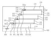
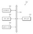
도 12는 본 발명의 실시 예들에 따른 반도체 패키지를 사용한 시스템을 나타낸 개략도이다.1 is a cross-sectional view of a semiconductor package according to a first embodiment of the present invention.
2A to 2I are sectional views sequentially illustrating a method of manufacturing a semiconductor package according to a first embodiment of the present invention.
3 is a flowchart illustrating a method of manufacturing a semiconductor package according to the first embodiment of the present invention.
4 is a cross-sectional view illustrating a semiconductor package according to a second embodiment of the present invention.
5A to 5E are cross-sectional views sequentially illustrating a method of manufacturing a semiconductor package according to a second embodiment of the present invention.
6 is a cross-sectional view of a semiconductor package according to a third embodiment of the present invention.
7A to 7G are sectional views sequentially illustrating a method of manufacturing a semiconductor package according to a third embodiment of the present invention.
8 is a cross-sectional view illustrating a semiconductor package according to a fourth embodiment of the present invention.
9A to 9D are cross-sectional views sequentially illustrating a method of manufacturing a semiconductor package according to a fourth embodiment of the present invention.
10 is a cross-sectional view of a semiconductor package according to a fifth embodiment of the present invention.
11A to 11C are sectional views sequentially illustrating a method of manufacturing a semiconductor package according to a fifth embodiment of the present invention.
12 is a schematic diagram showing a system using a semiconductor package according to embodiments of the present invention.
본 발명의 상기 목적과 기술적 구성 및 이에 따른 작용 효과에 관한 자세한 사항은 본 발명의 실시 예를 도시하고 있는 도면을 참조한 이하 상세한 설명에 의해 더욱 명확하게 이해될 것이다. 여기서, 본 발명의 실시 예들은 당업자에게 본 발명의 기술적 사상이 충분히 전달될 수 있도록 하기 위하여 제공되는 것이므로, 본 발명은 이하 설명되는 실시 예들에 한정되지 않도록 다른 형태로 구체화될 수 있다.DETAILED DESCRIPTION OF THE PREFERRED EMBODIMENTS Reference will now be made in detail to the preferred embodiments of the present invention, examples of which are illustrated in the accompanying drawings, wherein like reference numerals refer to the like elements throughout. Hereinafter, exemplary embodiments of the present invention will be described in detail with reference to the accompanying drawings. In the following description, well-known functions or constructions are not described in detail since they would obscure the invention in unnecessary detail.
또한, 명세서 전체에 걸쳐서 동일한 참조 번호로 표시된 부분들은 동일한 구성요소들을 의미하며, 도면들에 있어서 층 또는 영역의 길이와 두께는 편의를 위하여 과장되어 표현될 수 있다. 덧붙여, 제 1 구성 요소가 제 2 구성 요소 "상"에 있다고 기재되는 경우, 상기 제 1 구성 요소가 상기 제 2 구성 요소와 직접 접촉하는 상측에 위치하는 것뿐만 아니라, 상기 제 1 구성 요소와 제 2 구성 요소 사이에 제 3 구성 요소가 위치하는 경우도 포함한다.In the drawings, the same reference numerals denote the same components throughout the specification. In the drawings, the lengths and the thicknesses of layers or regions may be exaggerated for convenience. In addition, when the first component is described as being on the second component, it is preferable that the first component is located on the upper side in direct contact with the second component, 2 < / RTI > component is located between the two components.
여기서, 상기 제 1, 제 2 등의 용어는 다양한 구성 요소를 설명하기 위한 것으로, 하나의 구성 요소를 다른 구성 요소로부터 구별하는 목적으로 사용된다. 다만, 본 발명의 기술적 사상을 벗어나지 않는 범위에서는 제 1 구성 요소와 제 2 구성 요소는 당업자의 편의에 따라 임의로 명명될 수 있다.Here, the terms first, second, etc. are used for describing various components and are used for the purpose of distinguishing one component from another component. However, the first component and the second component may be arbitrarily named according to the convenience of the person skilled in the art without departing from the technical idea of the present invention.
본 발명의 명세서에서 사용하는 용어는 단지 특정한 실시 예를 설명하기 위해 사용되는 것으로, 본 발명을 한정하려는 의도가 아니다. 예를 들어, 단수로 표현된 구성 요소는 문맥상 명백하게 단수만을 의미하지 않는다면 복수의 구성 요소를 포함한다. 또한, 본 발명의 명세서에서, "포함하다" 또는 "가지다" 등의 용어는 명세서 상에 기재된 특징, 숫자, 단계, 동작, 구성 요소, 부분품 또는 이들을 조합한 것이 존재함을 지정하려는 것이지, 하나 또는 그 이상의 다른 특징들이나 숫자, 단계, 동작, 구성 요소, 부분품 또는 이들을 조합한 것들의 존재 또는 부가 가능성을 미리 배제하지 않는 것으로 이해되어야 한다.It is to be understood that the terminology used herein is for the purpose of describing particular embodiments only and is not intended to be limiting of the invention. For example, an element represented in singular form includes a plurality of elements unless the context clearly dictates a singular number. Also, in the specification of the present invention, the terms such as " comprises "or" having ", and the like, designate the presence of stated features, integers, steps, operations, elements, But do not preclude the presence or addition of one or more other features, numbers, steps, operations, components, parts, or combinations thereof.
덧붙여, 다르게 정의되지 않는 한, 기술적이거나 과학적인 용어를 포함해서 여기서 사용되는 모든 용어들은 본 발명이 속하는 기술 분야에서 통상의 지식을 가진 자에 의해 일반적으로 이해되는 것과 동일한 의미가 있다. 일반적으로 사용되는 사전에 정의되어 있는 것과 같은 용어들은 관련 기술의 문맥상 가지는 의미와 일치하는 의미가 있는 것으로 해석되어야 하며, 본 출원에서 명백하게 정의하지 않는 한, 이상적이거나 과도하게 형식적인 의미로 해석되지 않는다.
In addition, unless otherwise defined, all terms used herein, including technical or scientific terms, have the same meaning as commonly understood by one of ordinary skill in the art to which this invention belongs. Terms such as those defined in commonly used dictionaries are to be interpreted as having a meaning consistent with the meaning in the context of the relevant art and are to be construed as ideal or overly formal in meaning unless explicitly defined in the present application Do not.
(제 1 실시 예)(Embodiment 1)
도 1은 본 발명의 제 1 실시 예에 따른 반도체 패키지를 나타낸 단면도이다.1 is a cross-sectional view of a semiconductor package according to a first embodiment of the present invention.
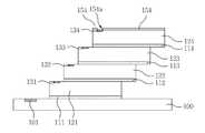
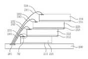
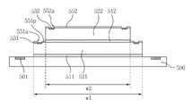
도 1을 참조하면, 본 발명의 제 1 실시 예에 따른 반도체 패키지는 제 1 배선 기판(100), 상기 제 1 배선 기판(100) 상에 상측 표면의 일부 영역들(D1)이 노출되도록 계단 형태로 적층되는 다수의 제 1 반도체 칩들(121 ~ 124), 상기 다수의 제 1 반도체 칩들(121 ~ 124)의 노출되는 상측 표면상에 형성된 다수의 제 1 보호막들(154, 161 ~ 164) 및 상기 다수의 제 1 반도체 칩들(121 ~ 124)의 측면과 상면을 덮는 제 1 몰딩막(molding layer, 170)을 포함할 수 있다.Referring to FIG. 1, a semiconductor package according to a first embodiment of the present invention includes a
여기서, 상기 다수의 제 1 반도체 칩들(121 ~ 124)은 설명의 편의 상 상기 제 1 배선 기판(100)으로부터 멀어지는 순으로 제 11 반도체 칩(121), 제 12 반도체 칩(122), 제 13 반도체 칩(123) 및 제 14 반도체 칩(124)이라 명명한다.The plurality of
본 발명의 제 1 실시 예에 따른 반도체 패키지는 상기 제 1 배선 기판(100)에 4개의 반도체 칩들(121 ~ 124)이 적층되는 것으로 설명된다. 그러나, 본 발명의 제 1 실시 예에 따른 반도체 패키지는 상기 제 1 배선 기판(100)에 5개 이상의 반도체 칩들(121 ~ 124)이 적층될 수 있다.The semiconductor package according to the first embodiment of the present invention is described in which four
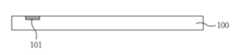
상기 제 1 배선 기판(100)은 인쇄회로기판(Printed Circuit Board; PCB), 리드 프레임(Lead Frame; LF), 테이프 배선, 세라믹 기판 및 이들의 조합으로 이루어진 그룹에서 선택된 하나일 수 있다. 여기서, 상기 인쇄회로기판(PCB)은 경성인쇄회로기판(Rigid PCB), 연성인쇄회로기판(Flexible PCB) 및 경연성인쇄회로기판(Rigid flexible PCB)으로 이루어진 그룹에서 선택된 하나일 수 있다.The
상기 제 1 배선 기판(100)은 상기 다수의 제 1 반도체 칩들(121 ~ 124)과 전기적으로 연결될 수 있다. 이를 위해 제 1 기판 패드(101)가 상기 제 1 배선 기판(100)의 일측 상에 형성될 수 있다. 상기 제 1 기판 패드(101)는 상기 제 1 배선 기판(100) 상에 형성된 전기 회로(미도시)로 전기 신호를 입력 또는 출력하기 위한 단자일 수 있다. 따라서, 상기 제 1 기판 패드(101)는 도전성 물질로 형성될 수 있다. 예를 들면, 상기 제 1 기판 패드(101)는 금(Au), 은(Ag), 구리(Cu), 니켈(Ni), 알루미늄(Al), 주석(Sn), 납(Pb), 백금(Pt), 비스무스(Bi), 인듐(In) 및 이들의 합금으로 이루어진 그룹에서 선택된 하나의 금속으로 형성될 수 있다.The
상기 제 1 기판 패드(101)는 상기 다수의 제 1 반도체 칩들(121 ~ 124)에 의해 상측 표면이 노출될 수 있다. 이를 위해 상기 제 1 기판 패드(101)는 상기 제 1 배선 기판(100)의 가장 자리에 형성될 수 있다.The upper surface of the
본 발명의 제 1 실시 예에 따른 반도체 패키지는 상기 제 1 기판 패드(101)가 상기 제 1 배선 기판(100) 상에 한 개가 형성되는 것으로 도시되었다. 그러나, 상기 제 1 기판 패드(101)는 상기 제 1 배선 기판(100) 상에 다수 개가 형성될 수 있다.In the semiconductor package according to the first embodiment of the present invention, one of the
상기 다수의 제 1 반도체 칩들(121 ~ 124)은 디램 칩(DRAM chip), 플래시 메모리 칩(flash memory chip), 상변화 메모리 칩(phase change memory chip), 엠램칩(magnetic random access memory chip; MRAM chip), 저항성 메모리 칩(resistive memory chip) 및 이들의 조합을 포함할 수 있다.The plurality of
상기 다수의 제 1 반도체 칩들(121 ~ 124)은 계단 형태로 적층될 수 있다. 따라서, 상기 다수의 제 1 반도체 칩들(121 ~ 124) 중 상대적으로 아래쪽에 위치하는 제 1 반도체 칩들(121 ~ 124)은 상대적으로 위쪽에 위치하는 제 1 반도체 칩들(121 ~ 124)에 의해 상측 표면 중 일부 영역(D1)이 노출될 수 있다.The plurality of
상기 다수의 제 1 반도체 칩들(121 ~ 124)은 각각 상기 일부 영역(D1) 상에 위치하는 제 1 칩 패드들(131 ~ 134)을 포함할 수 있다. 여기서, 상기 제 1 칩 패드들(131 ~ 134)은 상기 제 11 반도체 칩(121) 상에 위치하는 제 11 칩 패드(131), 상기 제 12 반도체 칩(121) 상에 위치하는 제 12 칩 패드(132), 상기 제 13 반도체 칩(121) 상에 위치하는 제 13 칩 패드(133) 및 상기 제 14 반도체 칩(121) 상에 위치하는 제 14 칩 패드(134)를 포함할 수 있다.The plurality of
상기 제 1 칩 패드들(131 ~ 134)은 상기 제 1 기판 패드(101)와 유사한 도전성 물질로 형성될 수 있다. 따라서, 상기 제 1 칩 패드들(131 ~ 134)은 금(Au), 은(Ag), 구리(Cu), 니켈(Ni), 알루미늄(Al), 주석(Sn), 납(Pb), 백금(Pt), 비스무스(Bi), 인듐(In) 및 이들의 합금으로 이루어진 그룹에서 선택된 하나의 금속으로 형성될 수 있다.The
상기 제 1 칩 패드들(131 ~ 134)은 제 1 본딩 와이어(141 ~ 144)들에 의해 상기 제 1 기판 패드(101)와 전기적으로 연결될 수 있다. 여기서, 상기 제 1 본딩 와이어들(141 ~ 144)은 연결되는 상기 제 1 칩 패드들(131 ~ 134)에 따라 제 11 본딩 와이어(141), 제 12 본딩 와이어(142), 제 13 본딩 와이어(143) 및 제 14 본딩 와이어(144)로 구분될 수 있다.The
본 발명의 제 1 실시 예에 따른 반도체 패키지는 상기 제 1 칩 패드들(131 ~ 134)의 일부 또는 전부가 상기 다수의 제 1 반도체 칩들(121 ~ 124)의 상측 표면 내에 매몰되는 것으로 도시되었다. 그러나, 본 발명의 제 1 실시 예에 따른 반도체 패키지는 상기 제 1 칩 패드들(131 ~ 134)의 일부 또는 전부가 상기 다수의 제 1 반도체 칩들(121 ~ 124) 각각의 상측 표면으로부터 돌출한 형태일 수 있다.In the semiconductor package according to the first embodiment of the present invention, some or all of the
상기 제 1 보호막들(154, 161 ~ 164)은 외부의 알파 입자(alpha particles) 또는 알파선(alpha-ray)으로부터 손상되는 것을 방지할 수 있다. 상기 제 1 보호막들(154, 161 ~ 164)은 제 11 내지 제 14 보호막들(161 ~ 164) 및 제 141 보호막(154)을 포함할 수 있다. 여기서, 상기 제 11 내지 제 13 보호막들은 상기 다수의 제 1 반도체 칩들(121 ~ 124) 각각의 상기 일부 영역(D1) 상에 형성될 수 있다. 또한, 상기 제141 보호막(154)은 상기 다수의 제 1 반도체 칩들(121 ~ 124) 중 최상측에 위치하는 상기 제 14 반도체 칩(124)의 상측 표면 상에 형성될 수 있다.The first
상기 제 11 내지 제14 보호막들(161 ~ 164)은 접착력을 가진 물질을 포함할 수 있다. 예를 들면, 상기 제 11 내지 제 14 보호막들(161 ~ 164)은 액상의 접착 물질로 형성될 수 있다. 상기 제 11 내지 제 14 보호막들(161 ~ 164)은 상기 제 1 칩 패드들(131 ~ 134)을 덮도록 형성될 수 있다.The eleventh to fourteenth
상기 제 141 보호막(154)은 감광성 폴리머를 포함할 수 있다. 상기 제 141 보호막(154)은 상기 다수의 제 1 반도체 칩들(121 ~ 124)이 상기 배선 기판(100)에 실장되기 전, 연마 공정 및 실장 공정에 의해 상기 반도체 칩들의 상부 표면 및/또는 상기 칩 패드들이 물리적, 화학적인 손상을 방지할 수 있다. 상기 제 141 보호막(154)은 상기 칩 패드(134)를 노출하기 위한 제 14 홀(154a)을 포함할 수 있다.The
상기 감광성 폴리머는 감광성 폴리 이미드(Photo Sensitive Poly Imide; PSPI)와 같이 감광성 성분이 포함된 열경화성 폴리머일 수 있다. 상기 열경화성 폴리머는 에폭시(epoxy), 폴리 이미드(polyimide), 노블락 페놀(novolak phenol), 폴리노르보넨(polynorbonene) 및 이들의 조합으로 이루어진 그룹에서 선택된 하나일 수 있다.The photosensitive polymer may be a thermosetting polymer containing a photosensitive component such as a photosensitive polyimide (PSPI). The thermosetting polymer may be selected from the group consisting of epoxy, polyimide, novolak phenol, polynorbonene, and combinations thereof.
본 발명의 제 1 실시 예에 따른 반도체 패키지는 상기 다수의 제 1 반도체 칩들(121 ~ 124) 사이 및 상기 제 1 배선 기판(100)과 상기 제 11 반도체 칩(121) 사이에 위치하는 다수의 제 1 접착층들(111 ~ 114)을 더 포함할 수 있다.The semiconductor package according to the first embodiment of the present invention includes a plurality of
여기서, 상기 제 1 접착층들(111 ~ 114)은 상기 제 11 반도체 칩(121)의 하부에 위치하는 제 11 접착층(111), 상기 제 12 반도체 칩(122)의 하부에 위치하는 제 12 접착층(112), 상기 제 13 반도체 칩(123)의 하부에 위치하는 제 13 접착층(113) 및 상기 제 14 반도체 칩(124)의 하부에 위치하는 제 14 접착층(114)을 포함할 수 있다.The first
상기 다수의 제 1 접착층들(111 ~ 114)은 디에이에프(Die Attach Film; DAF)일 수 있다. 상기 디에이에프(DAF)는 액상 또는 필름 형태의 에폭시 수지(epoxy resin)를 이용하여 형성될 수 있다.The plurality of first
본 발명의 제 1 실시 예에 따른 반도체 패키지는 상기 다수의 제 1 접착층들(111 ~ 114)이 각각 상기 다수의 제 1 반도체 칩들(121 ~ 124)의 하측 표면 상에 전체적으로 형성되는 것으로 도시하고 있다. 그러나, 상기 제 12 내지 제 14 접착층들(112 ~ 114)은 상기 상대적으로 아래쪽에 위치한 상기 제 11 내지 제 13 반도체 칩들(122 ~ 124)의 상부 표면과 접촉 또는 중첩되는 영역에만 형성될 수 있다. 즉, 본 발명의 제 1 실시 예에 따른 반도체 패키지는 상기 제 12 내지 제 14 반도체 칩들(122 ~ 124)의 아래쪽 표면의 일부가 노출될 수 있다.The semiconductor package according to the first embodiment of the present invention is shown in which the first
도 2a 내지 2i는 본 발명의 제 1 실시 예에 따른 반도체 패키지의 제조 방법을 순차적으로 나타낸 단면도들이다. 도 3은 본 발명의 제 1 실시 예에 따른 반도체 패키지의 제조 방법을 나타낸 공정 순서도이다.2A to 2I are sectional views sequentially illustrating a method of manufacturing a semiconductor package according to a first embodiment of the present invention. FIG. 3 is a flow chart showing the manufacturing method of the semiconductor package according to the first embodiment of the present invention.
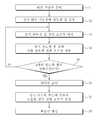
도 1, 도 2a 내지 2i 및 도 3을 참고하여 본 발명의 제 1 실시 예에 따른 반도체 패키지의 제조 방법을 설명한다. 먼저, 본 발명의 제 1 실시 예에 따른 반도체 패키지의 제조 방법은 도 2a에 도시된 바와 같이, 제 1 기판 패드(101)를 구비하는 제 1 배선 기판(100)을 준비하는 공정(S1)을 포함할 수 있다. 상기 배선 기판(100)은 인쇄회로기판(Printed Circuit Board; PCB), 리드 프레임(Lead Frame; LF), 테이프 배선, 세라믹 기판 및 이들의 조합으로 이루어진 그룹에서 선택된 하나일 수 있다.A method of manufacturing the semiconductor package according to the first embodiment of the present invention will be described with reference to Figs. 1, 2A to 2I and 3. Fig. First, as shown in FIG. 2A, a method of manufacturing a semiconductor package according to the first embodiment of the present invention includes a step S1 of preparing a
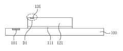
이어서, 본 발명의 제 1 실시 예에 따른 반도체 패키지의 제조 방법은 도 2b에 도시된 바와 같이, 상기 제 1 배선 기판(100) 상에 제 11 반도체 칩(121)을 실장하는 공정(S2)을 포함할 수 있다. 여기서, 상기 제 11 반도체 칩(121)은 상기 상기 제 1 기판 패드(101)의 상측 표면이 노출되도록 실장될 수 있다.Next, as shown in FIG. 2B, a method of manufacturing a semiconductor package according to the first embodiment of the present invention includes a step S2 of mounting an
상기 배선 기판(100)과 상기 제 11 반도체 칩(121) 사이에는 제 11 접착층(111)이 형성될 수 있다. 예를 들어, 상기 제 11 접착층(111)이 상기 제 11 반도체 칩(121)의 하측 표면에 형성된 후, 상기 제 11 반도체 칩(121)이 상기 배선 기판(100)에 실장될 수 있다. 또는, 상기 제 1 배선 기판(100) 상에 상기 제 11 접착층(111)이 형성되고, 상기 제 11 반도체 칩(121)이 실장될 수 있다.An eleventh
상기 제 11 접착층(111)은 디에이에프(DAF)일 수 있다. 상기 디에이에프(DAF)는 액상 또는 필름 형태의 에폭시 수지(epoxy resin)를 이용하여 형성될 수 있다.The eleventh
상기 제 11 접착층(111)은 상기 제 1 배선 기판(100) 상에 상기 제 11 반도체 칩(121)이 충분히 접착될 수 있도록 제 1 두께(h1)로 형성될 수 있다. 상기 제 1 두께(h1)는 10㎛ 내지 20㎛일 수 있다.The eleventh
상기 제 11 반도체 칩(121)은 상측 표면의 일부 영역(D1)에 위치하는 제 11 칩 패드(131)를 포함할 수 있다. 상기 일부 영역(D1)은 후속되는 제 12 반도체 칩(122)의 적층에 의해 노출되는 영역일 수 있다. 상기 제 11 칩 패드(131)는 상기 제 11 반도체 칩(121)의 상측 표면 상에 상기 제 1 기판 패드(101)와 가까운 가장 자리에 위치될 수 있다. 이에 따라 후속 공정을 통해 상기 제 11 칩 패드(131)와 상기 제 1 기판 패드(101)가 보다 용이하게 전기적으로 연결될 수 있다.The
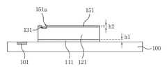
상기 제 11 반도체 칩(121)은 상측 표면을 덮는 제 111 보호막(151)을 포함할 수 있다. 상기 제 111 보호막(151)은 연마 공정 및 실장 공정 시, 상기 제 11 반도체 칩(121)이 손상되는 것을 방지할 수 있다. 상기 제 111 보호막(151)은 제 2 두께(h2)로 형성될 수 있다. 상기 제 2 두께(h2)는 5㎛ 내지 7㎛일 수 있다. 상기 제 111 보호막(151)은 감광성 폴리 이미드(PSPI)와 같은 감광성 폴리머 또는 자외선 테이프(UV tape)와 같은 보호 테이프일 수 있다. 상기 제 111 보호막(151)은 상기 제 11 칩 패드(131)의 표면의 일부 또는 전부를 노출시키는 제 11 홀(151a)을 포함할 수 있다. 상기 제 11 홀(151a)은 상기 제 11 반도체 칩(121)의 테스트를 위한 형성된 홀일 수 있다.The
다음으로, 본 발명의 제 1 실시 예에 따른 반도체 패키지의 제조 방법은 도 2c 내지 2e에 도시된 바와 같이, 상기 제 111 보호막(151)을 제거하는 공정(S3)을 포함할 수 있다. 예를 들어, 상기 제 111 보호막(151)을 제거하는 공정(S3)은 도 2c에 도시된 바와 같이, 상기 제 111 보호막(151)을 일정 용기(10)에 저장된 용매(11)에 담그는 것을 포함할 수 있다. 이를 위해 상기 제 11 반도체 칩(121)이 실장된 상기 배선 기판(100)은 상하가 역전될 수 있다.Next, a method of manufacturing the semiconductor package according to the first embodiment of the present invention may include a step (S3) of removing the 111st
상기 용매(11)는 KOH 및 Cu7OH와 같은 알칼리성 유기 용매일 수 있다. 상기 알칼리성 유기 용매는 상기 제 11 반도체 칩(121)과 상기 제 111 보호막(151) 사이의 계면 접착력을 약화시킬 수 있다.The solvent (11) can be used for alkaline organic solvents such as KOH and Cu7 OH. The alkaline organic solvent may weaken the interfacial adhesion between the
또한, 상기 제 111 보호막(151)을 제거하는 공정(S3)은 도 2d에 도시된 바와 같이, 흡입기(suction, 20)를 이용하여 상기 용매(11)에 젖은 상기 제 111 보호막(151)을 상기 제 11 반도체 칩(121)으로부터 분리하는 것을 포함할 수 있다. 이를 통해 본 발명의 제 1 실시 예에 따른 반도체 패키지의 제조 방법은 도 2e에 도시된 바와 같이, 상기 제 11 반도체 칩(121)의 상기 제 111 보호막(151)을 제거할 수 있다.The step of removing the 111
계속해서, 본 발명의 제 1 실시 예에 따른 반도체 패키지의 제조 방법은 도 2f에 도시된 바와 같이, 상기 제 11 반도체 칩(121) 상에 제 12 반도체 칩(122)을 오프셋 적층(offset stack)하는 공정(S4)을 포함할 수 있다. 여기서, 상기 오프셋 적층(offset stack)은 상기 제 12 반도체 칩(122)이 상기 제 11 반도체 칩(121)의 상측 표면 중 일부 영역(D1)이 노출되도록 적층되는 것을 의미한다.2F, the method of manufacturing a semiconductor package according to the first embodiment of the present invention includes offset stacking a
따라서, 본 발명의 제 1 실시 예에 따른 반도체 패키지의 제조 방법은 상기 제 12 반도체 칩(122)이 상기 제 11 반도체 칩(121)의 상측 표면 중 상기 일부 영역(D1)을 제외한 영역 상에 접촉 또는 중첩되도록 적층될 수 있다.Accordingly, in the method of manufacturing a semiconductor package according to the first embodiment of the present invention, the
상기 제 12 반도체 칩(122)은 상기 제 11 반도체 칩(121)과 유사하게 제 12 접착층(112)을 이용하여 적층될 수 있다. 즉, 상기 제 12 반도체 칩(122)은 하측 표면에 상기 제 12 접착층(112)이 형성된 후, 상기 제 11 반도체 칩(121) 상에 오프셋 적층될 수 있다. 상기 제 12 접착층(112)은 상기 제 11 접착층(111)의 상기 제 1 두께(h1)와 동일하거나 유사한 두께를 가질 수 있다.The
상기 제 12 반도체 칩(122)은 상측 표면의 일부 영역(D1)에 위치하는 제 12 칩 패드(132)를 포함할 수 있다. 상기 일부 영역(D1)은 앞서 설명한 것과 같이 후속되는 제 13 반도체 칩(123)의 적층에 의해 노출되는 상기 제 12 반도체 칩(122)의 상측 표면의 일부 영역(D1)일 수 있다. 상기 제 12 칩 패드(132)는 상기 제 12 반도체 칩(122)의 상측 표면 중 상기 제 1 기판 패드(101)와 가까운 가장 자리에 위치할 수 있다.The
상기 제 12 반도체 칩(122)은 상측 표면을 덮는 제121 보호막(152)을 포함할 수 있다. 상기 제 121 보호막(152)은 연마 공정 및 실장 공정 시, 상기 제 12 반도체 칩(122)이 손상되는 것을 방지할 수 있다. 상기 제 121 보호막(152)은 감광성 폴리 이미드(PSPI)와 같은 감광성 폴리머를 포함할 수 있다. 상기 제 121 보호막(152)은 상기 제 12 칩 패드(132)의 표면의 일부 또는 전부를 노출시키는 제 12 홀(152a)를 포함할 수 있다.The
이어서, 본 발명의 제 1 실시 예에 따른 반도체 패키지의 제조 방법은 상기 배선 기판(100) 상에 적층된 제 1 반도체 칩들(121 ~ 124)이 적층되기를 원하는 n개인지를 판단하는 공정(S6)을 포함할 수 있다. 여기서, 상기 배선 기판(100) 상에 적층된 제 1 반도체 칩들(121 ~ 124)이 n개 미만인 경우, 상기 S3 및 S4 공정을 반복하여 n 개의 반도체 칩들(121 ~ 124)이 적층될 수 있다.Next, a method of manufacturing a semiconductor package according to the first embodiment of the present invention includes a step (S6) of determining whether n is desired to stack the
본 발명의 제 1 실시 예에 따른 반도체 패키지는 4개의 제 1 반도체 칩들(121 ~ 124)이 적층된다. 따라서, 본 발명의 제 1 실시 예에 따른 반도체 패키지의 제조 방법은 도 2g에 도시된 바와 같이, 상기 배선 기판(100) 상에 4개의 제 1 반도체 칩들(121 ~ 124)이 적층되면 다음 공정이 수행될 수 있다. 여기서, 본 발명의 제 1 실시 예에 따른 반도체 패키지의 제조 방법은 상기 제 1 반도체 칩들(121 ~ 124) 중 최상측인 제 14 반도체 칩(124)의 상측 표면을 덮는 제 141 보호막(154)이 제거되지 않는다.In the semiconductor package according to the first embodiment of the present invention, four
상기 제 141 보호막(154)은 연마 공정 및 실장 공정 시, 상기 제 11 반도체 칩(121)이 손상되는 것을 방지할 수 있다. 상기 제 141 보호막(154)은 감광성 폴리 이미드(PSPI)와 같은 감광성 폴리머 또는 자외선 테이프(UV tape)와 같은 보호 테이프일 수 있다. 상기 제 141 보호막(154)은 상기 제 14 반도체 칩(124)의 상기 제 14 칩 패드(134)를 노출시키는 제 14 홀(154a)을 포함할 수 있다.The
다음으로, 본 발명의 제 1 실시 예에 따른 반도체 패키지의 제조 방법은 도 2h에 도시된 바와 같이, 상기 다수의 제 반도체 칩들(121 ~ 124) 각각의 제 1 칩 패드들(131 ~ 134) 사이 및 상기 제 11 칩 패드(131)와 상기 제 1 기판 패드(101) 사이를 본딩 와이어들(141 ~ 144)를 이용하여 전기적으로 연결시키는 공정(S6)을 포함할 수 있다.2H, a method of manufacturing a semiconductor package according to a first embodiment of the present invention includes the steps of: forming a plurality of
계속해서, 본 발명의 제 1 실시 예에 따른 반도체 패키지의 제조 방법은 도 2i에 도시된 바와 같이, 상기 제 11 내지 제 14 칩 패드들(131 ~ 134)을 덮도록 제 11 내지 제 14 보호막들(161 ~ 164)을 형성하는 공정(S7)을 포함할 수 있다. 여기서, 상기 제 11 내지 제 14 보호막들(161 ~ 164)은 상기 제 1 반도체 칩들(121 ~ 124)의 상기 일부 영역(D1)에 형성될 수 있다.As shown in FIG. 2I, the method for fabricating the semiconductor package according to the first embodiment of the present invention includes the eleventh to the fourteenth
상기 제 11 내지 제 13 반도체 칩들(121 ~ 123)은 상측 표면의 일부 영역(D1)이 노출되도록 계단 형태로 적층될 수 있다. 이에 따라, 상기 제 11 내지 제 14 칩 패드들(131 ~ 134)은 단차를 가지며 노출될 수 있다. 따라서, 상기 제 11 내지 제 14 보호막들(161 ~ 164)은 상기 제 11 내지 제 14 칩 패드들(131 ~ 134) 사이의 단차에 무관하게 상기 제 11 내지 제 14 칩 패드(131 ~ 134)를 균일하게 덮도록 형성될 수 있다.The eleventh to
예를 들어, 상기 제 11 내지 제 14 보호막들(161 ~ 164)을 형성하는 방법은 접착성을 갖는 액상의 소스를 분사하여 형성하는 방법 또는 소스를 증발시켜 형성하는 방법을 포함할 수 있다. 상기 액상의 소스는 분사 및 증발이 용이하므로, 상기 제 11 내지 제 14 보호막들(161 ~ 164)이 용이하게 형성될 수 있다. 상기 액상의 소스는 감광성 폴리머가 아닌 액상의 폴리머일 수 있다. 이에 따라, 상기 제 11 내지 제 14 보호막들(161 ~ 164)은 상기 제 14 반도체 칩(124)의 상측 표면을 덮는 상기 제 141 보호막(154)과 상이한 물질로 형성될 수 있다.For example, the method of forming the eleventh to fourteenth
상기 제 11 내지 제 14 보호막들(161 ~ 164)은 후속되는 상기 다수의 제 1 칩 패드들(131 ~ 134)이 외부의 알파 입자(alpha particles) 또는 알파선(alpha-ray)으로부터 손상되는 것을 방지할 수 있다. 따라서 상기 제 11 내지 제 13 보호막(161 ~ 164)은 상기 제 11 내지 제 13 칩 패드들(131 ~ 133)을 충분히 덮을 수 있는 제 3 두께(h3)를 가질 수 있다.The first to fourth
이어서, 본 발명의 제 1 실시 예에 따른 반도체 패키지의 제조 방법은 도 1에 도시된 바와 같이, 상기 다수의 제 1 반도체 칩들(121 ~ 124)의 측면 및 상면을 덮는 제 1 몰딩막(170)을 형성하는 공정(S8)을 포함할 수 있다. 이에 따라 본 발명의 제 1 실시 예에 따른 반도체 패키지가 완성될 수 있다. 상기 제 1 몰딩막(170)은 이엠씨(Epoxy Molding Compound; EMC)로 형성될 수 있다.1, a method of manufacturing a semiconductor package according to a first embodiment of the present invention includes a
여기서, 본 발명의 제 1 실시 예에 따른 반도체 패키지의 제조 방법은 상기 제 1 몰딩막(170)을 형성하기 전, 상기 제 11 내지 제 14 보호막들(161 ~ 164)에 함유된 솔벤트(solvent)를 제거하는 공정을 포함할 수 있다. 이에 따라 상기 제 11 내지 제 14 보호막(161 ~ 164)의 상기 제 3 두께(h3)은 감소할 수 있다.Here, the method of manufacturing a semiconductor package according to the first embodiment of the present invention may further include removing a solvent contained in the eleventh to fourteenth
결과적으로 본 발명의 제 1 실시 예에 따른 반도체 패키지 및 그의 제조 방법은 연마 공정 및 실장 공정에 의한 손상을 방지하는 보호막을 제거한 후, 다음 반도체 칩을 오프셋 적층한다. 이에 따라 계단형으로 적층되는 다수의 반도체 칩들 사이에는 보호막이 위치하지 않게 된다. 따라서, 상기 반도체 패키지에 적층되는 반도체 칩의 체적이 감소될 수 있다.
As a result, the semiconductor package and the manufacturing method thereof according to the first embodiment of the present invention remove the protective film for preventing damage due to the polishing process and the mounting process, and then offset stack the next semiconductor chip. Accordingly, the protective film is not located between the plurality of semiconductor chips stacked in a step-like manner. Therefore, the volume of the semiconductor chip stacked on the semiconductor package can be reduced.
(제 2 실시 예)(Second Embodiment)
도 4는 본 발명의 제 2 실시 예에 따른 반도체 패키지를 나타낸 단면도이다.4 is a cross-sectional view illustrating a semiconductor package according to a second embodiment of the present invention.
도 4를 참조하면, 본 발명의 제 2 실시 예에 따른 반도체 패키지는 제 2 배선 기판(200), 상기 제 2 배선 기판(200) 상에 상측 표면의 일부 영역들(D2)이 노출되도록 계단 형태로 적층되는 다수의 제 2 반도체 칩들(221 ~ 224), 상기 다수의 제 2 반도체 칩들(221 ~ 224)의 노출된 일부 영역들(D2)과 상기 다수의 제 2 반도체 칩들(221 ~ 224) 중 최상측에 위치하는 제 24 반도체 칩(224)의 상측 표면을 덮는 다수의 제 2 보호막들(261 ~ 264) 및 상기 제 2 반도체 칩들(221 ~ 224)의 측면 및 상면을 덮는 제 2 몰딩막(270)을 포함할 수 있다.Referring to FIG. 4, the semiconductor package according to the second embodiment of the present invention includes a
여기서, 본 발명의 제 1 실시 예와 유사하게 상기 다수의 제 2 반도체 칩들(221 ~ 224)은 상기 제 2 배선 기판(200)으로부터 멀어지는 순으로 제 21 반도체 칩(221), 제 22 반도체 칩(222), 제 23 반도체 칩(223) 및 제 24 반도체 칩(224)이라 명명한다.Similar to the first embodiment of the present invention, the plurality of
상기 제 2 배선 기판(200), 상기 다수의 제 2 반도체 칩들(221 ~ 224) 및 제 2 몰딩막(270)은 본 발명의 제 1 실시 예에 따른 반도체 패키지의 상기 제 1 배선 기판(100), 상기 다수의 제 1 반도체 칩들(121 ~ 124) 및 제 1 몰딩막(170)과 동일한 구성 요소로 이해될 수 있을 것이다. 따라서, 여기서는 구체적인 설명이 생략된다.The
또한, 본 발명의 제 2 실시 예에 따른 반도체 패키지는 본 발명의 제 1 실시 예에 따른 반도체 패키지의 상기 제 1 기판 패드(101), 상기 다수의 제 1 접착층들(111 ~ 114) 및 상기 다수의 제 1 칩 패드들(131 ~ 134)와 유사한 구성인 제 2 기판 패드(201), 다수의 제 2 접착층들(211 ~ 214) 및 다수의 제 2 칩 패드들(231 ~ 234)이 개시된다. 따라서, 이에 대한 설명은 본 발명의 제 1 실시 예에서 설명한 내용으로부터 이해될 수 있을 것이다.In addition, the semiconductor package according to the second embodiment of the present invention includes the
이하에서는 본 발명의 제 1 실시 예에 따른 반도체 패키지와 상이한 점만을 간략히 설명하기로 한다.Hereinafter, only the differences from the semiconductor package according to the first embodiment of the present invention will be described briefly.
본 발명의 제 2 실시 예에 따른 반도체 패키지는 상기 다수의 제 2 반도체 칩들(221 ~ 224)의 제 2 칩 패드들(231 ~ 234)이 본딩 와이어들(241 ~ 244)에 의해 각각 상기 제 2 기판 패드(201)와 전기적으로 연결될 수 있다. 즉, 상기 다수의 제 2 반도체 칩들(221 ~ 224)은 상기 제 2 배선 기판(200)과 개별적으로 전기적 연결될 수 있다.The semiconductor package according to the second embodiment of the present invention is characterized in that the
상기 제 2 보호막들(261 ~ 264)은 상기 다수의 제 2 반도체 칩들(221 ~ 224) 각각의 상측 표면 중 일부 영역들(D2)을 덮는 제 21 내지 제 24 보호막들(261 ~ 264) 및 최상측에 위치하는 상기 제 24 반도체 칩(224)의 상측 표면을 덮는 제 24 보호막(264)을 포함할 수 있다.The second
상기 제 21 내지 24 보호막(261 ~ 264)은 상기 다수의 제 2 반도체 칩들(221 ~ 224)이 외부의 알파 입자 또는 알파선으로부터 손상되는 것을 방지할 수 있다. 상기 제 21 내지 제 24 보호막(261 ~ 264)은 상기 제 2 칩 패드들(231 ~ 234)을 노출시키는 제 2 홀들(251a ~ 254a)을 포함할 수 있다.The 21st to 24th
상기 제 21 내지 제 23 보호막들(261 ~ 263)과 상기 제 24 보호막(264)은 동일한 물질로 형성될 수 있다. 상기 제 11 내지 제14 보호막들(161 ~ 164)은 접착력을 가진 물질을 포함할 수 있다. 예를 들면, 상기 제 11 내지 제 14 보호막들(161 ~ 164)은 액상의 접착 물질로 형성될 수 있다. 상기 제 21 내지 제 24 보호막(261 ~ 264)은 감광성 폴리 이미드(PSPI)와 같은 감광성 폴리머일 수 있다.The 21st to 23rd
도 5a 내지 5e는 본 발명의 제 2 실시 예에 따른 반도체 패키지의 제조 방법을 순차적으로 나타낸 단면도들이다. 이하에서는 본 발명의 제 1 실시 예에 따른 반도체 패키지의 제조 방법과 비교하여 상이한 점만을 간략히 설명한다.5A to 5E are cross-sectional views sequentially illustrating a method of manufacturing a semiconductor package according to a second embodiment of the present invention. Hereinafter, only differences from the method of manufacturing a semiconductor package according to the first embodiment of the present invention will be described briefly.
본 발명의 제 2 실시 예에 따른 반도체 패키지의 제조 방법은 도 5a에 도시된 바와 같이, 제 2 배선 기판(200)에 제 21 칩 패드(231) 및 제 211 보호막(251)을 포함하는 제 21 반도체 칩(221)을 실장하는 공정을 포함할 수 있다. 상기 제 211 보호막(251)은 상기 제 21 반도체 칩들(221)이 연마 공정 및 실장 공정에 의해 상기 반도체 칩들의 상부 표면 및/또는 상기 칩 패드들이 물리적, 화학적인 손상되는 것을 방지할 수 있다. 상기 제 141 보호막(154)은 감광성 폴리 이미드(PSPI)와 같은 감광성 폴리머 또는 자외선 테이프(UV tape)와 같은 보호 테이프일 수 있다. 상기 제 211 보호막(251)은 상기 제 21 칩 패드(231)를 노출시키는 제 21 홀(251a)을 포함할 수 있다.5A, a method of manufacturing a semiconductor package according to a second embodiment of the present invention includes a step of forming a second semiconductor chip on a
이어서, 본 발명의 제 2 실시 예에 따른 반도체 패키지의 제조 방법은 도 5b 및 5c에 도시된 바와 같이, 상기 제 21 반도체 칩(221) 상에 레이저(laser) 또는 자외선(UV)을 조사하여 상기 제 211 보호막(251)을 제거하는 공정을 포함할 수 있다. 여기서, 상기 제 21 반도체 칩(221) 상에 상기 자외선(UV)을 조사하는 공정은 상기 제 211 보호막(251)이 자외선 테이프(UV tape)인 경우에 수행할 수 있다.5B and 5C, a method of manufacturing a semiconductor package according to a second embodiment of the present invention includes irradiating a laser or ultraviolet (UV) light onto the twenty-
다음으로, 본 발명의 제 2 실시 예에 따른 반도체 패키지의 제조 방법은 도 5d에 도시된 바와 같이, 앞서 설명한 공정을 반복 수행하여 상기 제 21 반도체 칩(221) 상에 제 22 내지 제 24 반도체 칩(222 ~ 224)을 오프셋 적층(offset stack)하는 공정을 포함할 수 있다. 여기서, 상기 오프셋 적층(offset stack)은 상대적으로 위쪽에 배치된 제 22 내지 제 24 반도체 칩(222 ~ 224)이 상대적으로 아래쪽에 배치된 제 21 내지 제 23 반도체 칩(221 ~ 223)의 상측 표면 중 일부 영역(D2)이 노출되도록 적층되는 것을 의미한다. 상기 일부 영역(D2)은 후속되는 공정을 통해 적층되는 상기 제 22 내지 제 24 반도체 칩(222 ~ 224)에 의해 노출되는 상기 제 21 내지 제 23 반도체 칩(221 ~ 223)의 상측 표면일 수 있다.Next, as shown in FIG. 5D, the manufacturing method of the semiconductor package according to the second embodiment of the present invention repeats the above-described processes to form twenty-second to twenty-fourth semiconductor chips And offset stacking the first to
따라서, 본 발명의 제 2 실시 예에 따른 반도체 패키지의 제조 방법은 제 2 반도체 칩들(221 ~ 224) 중 최상측에 위치하는 제 24 반도체 칩(224)의 상측 표면을 덮는 제 254 보호막(미도시)이 제거된 후, 다음 공정이 수행될 수 있다.Therefore, the manufacturing method of the semiconductor package according to the second embodiment of the present invention is characterized in that the 254 protection film (not shown) covering the upper surface of the
계속해서, 본 발명의 제 2 실시 예에 따른 반도체 패키지의 제조 방법은 도 5e에 도시된 바와 같이, 상기 제 2 반도체 칩들(221 ~ 224) 각각의 제 2 칩 패드들(231 ~ 234)을 본딩 와이어들(241 ~ 244)을 이용하여 상기 제 2 기판 패드(201)와 전기적으로 연결하는 공정을 포함할 수 있다.5E, the method of manufacturing a semiconductor package according to the second embodiment of the present invention includes bonding the
이어서, 본 발명의 제 2 실시 예에 따른 반도체 패키지의 제조 방법은 도 4에 도시된 바와 같이, 상기 다수의 제 2 반도체 칩들(221 ~ 224)의 상기 일부 영역(D2) 및 상기 제 24 반도체 칩(224)의 상측 표면 상에 제 21 내지 제 24 보호막들(261 ~ 264)을 형성하는 공정을 포함할 수 있다. 여기서, 상기 제 21 내지 제 24 보호막들(161 ~ 164)은 덮는 상기 제 21 내지 제 24 칩 패드들(231 ~ 234)을 덮을 수 있다.4, the method of manufacturing a semiconductor package according to the second embodiment of the present invention includes the step of forming the partial regions D2 of the plurality of
결과적으로 본 발명의 제 2 실시 예에 따른 반도체 패키지 및 그의 제조 방법은 레이저 또는 자외선을 이용하여 각 반도체 칩 상에 형성된 연마 공정 및 실장 공정에 의한 손상을 방지하는 보호막을 제거하며 오프셋 적층한다. 이어서, 다수의 반도체 칩을 원하는 개수만큼 적층하고 와이어 본딩한다. 다음으로, 상기 다수의 반도체 칩의 노출된 상측 표면 상에 액체 소스를 이용하여 보호막을 형성한다. 따라서, 상대적으로 간소화된 공정으로 상기 반도체 패키지에 적층되는 반도체 칩의 체적이 감소될 수 있다.
As a result, the semiconductor package and the method for fabricating the same according to the second embodiment of the present invention remove the protective film for preventing damage due to the polishing process and the mounting process formed on each semiconductor chip by using laser or ultraviolet rays and offset them. Then, a desired number of semiconductor chips are stacked and wire-bonded. Next, a protective film is formed by using a liquid source on the exposed upper surface of the plurality of semiconductor chips. Therefore, the volume of the semiconductor chip stacked on the semiconductor package can be reduced by a relatively simplified process.
(제 3 실시 예)(Third Embodiment)
도 6은 본 발명의 제 3 실시 예에 따른 반도체 패키지를 나타낸 단면도이다.6 is a cross-sectional view of a semiconductor package according to a third embodiment of the present invention.
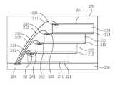
도 6을 참조하면, 본 발명의 제 3 실시 예에 따른 반도체 패키지는 제 3 배선 기판(300), 상기 제 3 배선 기판(300)에 지그재그(zigzag) 형태로 적층되는 다수의 제 3 반도체 칩들(321 ~ 324), 상기 다수의 제 3 반도체 칩들(321 ~ 324)의 노출된 일부 영역(D3)과 상기 다수의 제 3 반도체 칩들(321 ~ 324) 중 최상측에 위치하는 제 34 반도체 칩(324)의 상측 표면을 덮는 다수의 제 3 보호막들(351p ~ 353p, 354) 및 상기 제 3 반도체 칩들(321 ~ 324)의 측면 및 상면을 덮는 제 3 몰딩막(370)을 포함할 수 있다.Referring to FIG. 6, the semiconductor package according to the third embodiment of the present invention includes a
여기서, 본 발명의 제 1 실시 예와 유사하게 상기 다수의 제 3 반도체 칩들(321 ~ 324)은 상기 제 3 배선 기판(300)으로부터 멀어지는 순으로 제 31 반도체 칩(321), 제 32 반도체 칩(322), 제 33 반도체 칩(323) 및 제 34 반도체 칩(324)이라 명명한다.Here, similarly to the first embodiment of the present invention, the plurality of
상기 제 3 배선 기판(300), 상기 다수의 제 3 반도체 칩들(321 ~ 324) 및 제 3 몰딩막(370)은 본 발명의 제 1 실시 예에 따른 반도체 패키지의 상기 제 1 배선 기판(100), 상기 다수의 제 1 반도체 칩들(121 ~ 124) 및 상기 제 1 몰딩막(170)과 동일한 구성 요소로 이해될 수 있을 것이다. 따라서, 여기서는 구체적인 설명이 생략된다.The
또한, 본 발명의 제 3 실시 예에 따른 반도체 패키지는 본 발명의 제 2 실시 예에 따른 반도체 패키지의 상기 다수의 제 2 접착층들(211 ~ 214), 상기 다수의 제 2 칩 패드들(231 ~ 234), 상기 제 2 본딩 와이어들(241 ~ 244) 및 상기 다수의 제 2 보호막들(251p ~ 253p, 254)과 유사한 구성인 다수의 제 3 접착층들(311 ~ 314), 다수의 제 3 칩 패드들(331 ~ 334), 제 3 본딩 와이어들(341 ~ 344) 및 다수의 제 3 보호막들(351p ~ 353p, 354)이 개시된다. 따라서, 이에 대한 설명은 본 발명의 제 1 실시 예에서 설명한 내용 및 본 발명의 제 2 실시 예에서 설명한 내용으로부터 이해될 수 있을 것이다.In addition, the semiconductor package according to the third embodiment of the present invention includes the plurality of second
이하에서는 본 발명의 제 1 실시 예에 따른 반도체 패키지 및 본 발명의 제 2 실시 예에 따른 반도에 패키지와 상이한 점만을 간략히 설명하기로 한다.Hereinafter, only the differences between the semiconductor package according to the first embodiment of the present invention and the package according to the second embodiment of the present invention will be described briefly.
상기 다수의 제 3 반도체 칩들(321 ~ 324)은 지그재그(zigzag) 형태로 적층될 수 있다. 따라서, 상기 제 3 반도체 칩들(321 ~ 324)은 상부에 인접하게 위치하는 반도체 칩들(321 ~ 324)에 의해 노출되는 일부 영역(D3)이 지그재그 형태로 위치할 수 있다. 또한, 상기 제 3 반도체 칩들(321 ~ 324) 각각의 일부 영역(D3)에 위치하는 다수의 제 3 칩 패드들(331 ~ 334)도 지그재그 형태로 위치할 수 있다.The plurality of
이에 따라 상기 제 3 배선 기판(300)은 상측 표면의 일측에 위치하는 제 31 기판 패드(301) 및 상측 표면의 타측에 위치하는 제 32 기판 패드(302)를 포함할 수 있다. 상기 제 31 기판 패드(301) 및 상기 제 32 기판 패드(302)는 동일 금속 물질로 형성될 수 있다. 예를 들면, 상기 제 3 기판 패드(301) 및 상기 제 32 기판 패드(302)는 금(Au), 은(Ag), 구리(Cu), 니켈(Ni), 알루미늄(Al), 주석(Sn), 납(Pb), 백금(Pt), 비스무스(Bi), 인듐(In) 및 이들의 합금으로 이루어진 그룹에서 선택된 하나의 금속으로 동일하게 형성될 수 있다.Accordingly, the
상기 제 3 칩 패드들(331 ~ 334)은 상기 다수의 제 3 반도체 칩들(321 ~ 324)의 적층된 위치에 따라 상기 제 31 기판 패드(301) 또는 상기 제 32 기판 패드(302)에 전기적으로 연결될 수 있다. 예를 들면, 상기 제 31 칩 패드(331) 및 상기 제 33 칩 패드(333)는 상기 제 31 기판 패드(301)에 전기적으로 연결될 수 있다. 상기 제 32 칩 패드(332) 및 상기 제 34 칩 패드(334)는 상기 제 32 기판 패드(302)에 전기적으로 연결될 수 있다.The
도 7a 내지 7g는 본 발명의 제 3 실시 예에 따른 반도체 패키지의 제조 방법을 순차적으로 나타낸 단면도들이다. 이하에서는 본 발명의 제 1 실시 예에 따른 반도체 패키지의 제조 방법 및 제 2 실시 예에 따른 반도체 패키지의 제조 방법과 상이한 점만을 간략히 설명한다.7A to 7G are sectional views sequentially illustrating a method of manufacturing a semiconductor package according to a third embodiment of the present invention. Hereinafter, only the differences between the method of manufacturing the semiconductor package according to the first embodiment of the present invention and the method of manufacturing the semiconductor package according to the second embodiment will be briefly described.
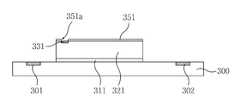
본 발명의 제 3 실시 예에 따른 반도체 패키지의 제조 방법은 도 7a에 도시된 바와 같이, 제 31 기판 패드(301) 및 제 32 기판 패드(302)를 구비하는 제 3 배선 기판(300) 상에 제 31 반도체 칩(221)을 실장하는 공정을 포함할 수 있다. 상기 제 31 기판 패드(301) 및 상기 제 32 기판 패드(302)는 상기 제 3 배선 기판(300)의 양측 가장 자리에 각각 형성될 수 있다. 상기 제 31 반도체 칩(321)은 제 31 칩 패드(331) 및 제 311 보호막(351)을 포함할 수 있다. 상기 제 311 보호막(351)은 상기 제 31 칩 패드(331)을 노출시키는 제 31 홀(351a)를 포함할 수 있다. 여기서, 상기 제 31 홀(351a)는 상기 제 31 반도체 칩(321)의 테스트를 위한 형성된 홀일 수 있다.A method of manufacturing a semiconductor package according to a third embodiment of the present invention is a method of manufacturing a semiconductor package including a
이어서, 본 발명의 제 3 실시 예에 따른 반도체 패키지의 제조 방법은 도 7b에 도시된 바와 같이, 상기 제 31 반도체 칩(221) 상에 일부 영역(D3)을 노출하는 마스크 패턴(350)을 형성하는 공정을 포함할 수 있다. 상기 일부 영역(D3)은 후속되는 제 32 반도체 칩(323)의 적층에 의해 노출되는 상기 제 31 반도체 칩(321)의 상측 표면일 수 있다.Next, as shown in FIG. 7B, a method of manufacturing a semiconductor package according to the third embodiment of the present invention includes forming a
다음으로, 본 발명의 제 3 실시 예에 따른 반도체 패키지의 제조 방법은 도 7c에 도시된 바와 같이, 상기 마스크 패턴(350)을 이용하여 상기 제 311 보호막(351)을 식각하여 제 31 보호막(351p)을 형성하는 공정을 포함할 수 있다. 상기 제 31 보호막(351p)는 상기 제 31 홀(351a)을 포함할 수 있다.Next, as shown in FIG. 7C, the method for fabricating a semiconductor package according to the third embodiment of the present invention includes etching the 311
계속해서, 본 발명의 제 3 실시 예에 따른 반도체 패키지의 제조 방법은 도 7d에 도시된 바와 같이, 제 31 본딩 와이어(341)에 의해 상기 제 31 칩 패드(331)와 상기 제 31 기판 패드(301)가 전기적으로 연결되는 공정을 포함할 수 있다.As shown in FIG. 7D, the method of manufacturing a semiconductor package according to the third embodiment of the present invention includes forming the
이어서, 본 발명의 제 3 실시 예에 따른 반도체 패키지의 제조 방법은 도 7e에 도시된 바와 같이, 제 32 반도체 칩(322)이 상기 제 31 반도체 칩(321) 상에 오프셋 적층(offset stack)되는 공정을 포함할 수 있다. 상기 오프셋 적층(offset stack)은 상기 제 31 반도체 칩(321)의 상기 일부 영역(D3)이 노출되도록 상기 제 32 반도체 칩(322)이 적층되는 것을 의미한다.7E, a
상기 제 32 반도체 칩(322)은 제 32 칩 패드(332) 및 제 321 보호막(352)을 포함할 수 있다. 상기 제 321 보호막(352)은 상기 제 32 칩 패드(332)을 노출시키는 제 32 홀(352a)를 포함할 수 있다.The thirty-
상기 제 32 반도체 칩(322)의 상기 제 32 칩 패드(332)는 상기 제 31 반도체 칩(321)의 제 31 칩 패드(331)와 비교하여 반대측 가장 자리에 위치할 수 있다. 예를 들면, 상기 제 31 칩 패드(331)는 상기 제 31 반도체 칩(321)의 좌측 표면에 위치하고, 상기 제 32 칩 패드(332)는 상기 제 32 반도체 칩(322)의 우측 표면에 위치할 수 있다.The thirty-
다음으로, 본 발명의 제 3 실시 예에 따른 반도체 패키지의 제조 방법은 도 7f에 도시된 바와 같이, 상기 제 321 보호막(352)의 일부를 제거하여 제 32 보호막(352p)을 형성하는 공정을 포함할 수 있다. 상기 제 32 보호막(352p)은 상기 제 32 홀(352a)을 포함할 수 있다. 상기 제 321 보호막(352)의 일부를 제거하는 공정은 상기 제 311 보호막(351)의 일부를 제거하는 공정과 유사하게 마스크 패턴(350)을 이용하여 수행할 수 있다.Next, a method of manufacturing a semiconductor package according to a third embodiment of the present invention includes a step of removing a part of the
여기서, 앞서 설명한 바와 같이, 상기 제 32 칩 패드(332)는 상기 제 31 칩 패드(331)과 반대측 가장 자리에 위치할 수 있다. 이에 따라, 상기 제 32 보호막(352p)는 상기 제 31 보호막(352p)와 반대측 가장 자리에 위치할 수 있다. 따라서, 상기 제 322 보호막(352)은 상기 제 31 반도체 칩(321)과 중첩되는 영역이 제거될 수 있다.Here, as described above, the
계속해서, 본 발명의 제 3 실시 예에 따른 반도체 패키지의 제조 방법은 제 32 본딩 와이어(342)에 의해 상기 제 32 칩 패드(332)와 상기 제 32 기판 패드(302)가 전기적으로 연결되는 공정을 포함할 수 있다.The method for fabricating a semiconductor package according to the third embodiment of the present invention includes a step of electrically connecting the
이어서, 본 발명의 제 3 실시 예에 따른 반도체 패키지의 제조 방법은 도 7g에 도시된 바와 같이, 제 33 반도체 칩(323)이 상기 제 32 반도체 칩(322) 상에 오프셋 적층(offset stack)되는 공정을 포함할 수 있다. 이에 따라 상기 제 33 반도체 칩(323)은 상기 제 31 반도체 칩(321)과 중첩되는 영역에 적층될 수 있다.7G, a
결과적으로 본 발명의 제 3 실시 예에 따른 반도체 패키지 및 그의 제조 방법은 각 반도체 칩 상의 보호막을 적층되는 순서에 따라 지그재그로 제거할 수 있다. 이어서, 다음 반도체 칩이 상기 보호막이 제거된 영역에 적층된다. 이에 따라, 본 발명의 제 3 실시 예에 따른 반도체 패키지 및 그의 제조 방법은 지그재그 형태로 적층되는 다수의 반도체 칩들의 체적을 감소시킬 수 있다.
As a result, the semiconductor package and the method of manufacturing the same according to the third embodiment of the present invention can remove the protective films on each semiconductor chip by zigzags in the order of stacking. Then, the next semiconductor chip is stacked on the region where the protective film is removed. Accordingly, the semiconductor package and the manufacturing method thereof according to the third embodiment of the present invention can reduce the volume of a plurality of semiconductor chips stacked in a zigzag form.
(제 4 실시 예)(Fourth Embodiment)
도 8은 본 발명의 제 4 실시 예에 따른 반도체 패키지를 나타낸 단면도이다.8 is a cross-sectional view illustrating a semiconductor package according to a fourth embodiment of the present invention.
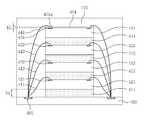
도 8을 참조하면, 본 발명의 제 4 실시 예에 따른 반도체 패키지는 제 4 배선 기판(400), 상기 제 4 배선 기판(400)에 수직 적층되는 다수의 제 4 반도체 칩들(421 ~ 424), 상기 다수의 제 4 반도체 칩들(421 ~ 424) 중 최상측에 위치하는 제 44 반도체 칩(424)을 덮는 제 4 보호막(454) 및 상기 다수의 제 4 반도체 칩들(421 ~ 424)을 덮는 제 4 몰딩막(470)을 포함할 수 있다.8, the semiconductor package according to the fourth embodiment of the present invention includes a
여기서, 본 발명의 제 1 실시 예와 유사하게 상기 다수의 제 4 반도체 칩들(421 ~ 424)은 상기 제 4 배선 기판(400)으로부터 멀어지는 순으로 제 41 반도체 칩(421), 제 42 반도체 칩(422), 제 43 반도체 칩(423) 및 제 44 반도체 칩(424)이라 명명한다.Similarly to the first embodiment of the present invention, the plurality of
상기 제 4 배선 기판(400), 상기 다수의 제 4 반도체 칩들(421 ~ 424), 상기 제 4 보호막(454) 및 제 4 몰딩막(470)은 본 발명의 제 1 실시 예에 따른 반도체 패키지의 상기 제 1 배선 기판(100), 상기 다수의 제 1 반도체 칩들(121 ~ 124), 상기 제 141 보호막(154) 및 제 1 몰딩막(170)과 동일한 구성 요소로 이해될 것이다. 따라서, 여기서는 구체적인 설명이 생략된다.The
또한, 본 발명의 제 4 실시 예에 따른 반도체 패키지는 본 발명의 제 1 내지 제 3 실시 예에 따른 반도체 패키지에 개시된 것과 유사한 구성인 다수의 제 4 접착층들(411 ~ 414), 다수의 제 4 칩 패드들(431 ~ 434), 제 4 본딩 와이어들(441 ~ 444) 및 다수의 제 4 보호막(454)이 개시된다. 따라서, 이에 대한 설명은 본 발명의 제 1 내지 제 4 실시 예에서 설명한 내용에서 설명한 내용으로부터 이해될 수 있을 것이다.In addition, the semiconductor package according to the fourth embodiment of the present invention includes a plurality of fourth
이하에서는 본 발명의 제 1 내지 제 4 실시 예에 따른 반도체 패키지와 상이한 점만을 간략히 설명하기로 한다.Hereinafter, only the differences from the semiconductor packages according to the first to fourth embodiments of the present invention will be described briefly.
본 발명의 제 4 실시 예에 따른 반도체 패키지는 상기 다수의 제 4 반도체 칩들(421 ~ 424)가 수직 적층될 수 있다. 이에 따라, 상기 칩 패드들(431 ~ 434)는 상기 다수의 제 4 반도체 칩들(421 ~ 424) 사이에 위치할 수 있다. 따라서, 제 4 본딩 와이어들(441 ~ 444)이 각 반도체 칩들(421 ~ 424)의 상부에 인접하게 적층된 반도체 칩들(421 ~ 424)의 하측 표면에 접촉하지 않도록 상기 제 4 접착층들(411 ~ 414)은 제 4 두께(h4)를 가질 수 있다. 상기 제 4 두께(h4)는 60㎛ 내지 80㎛일 수 있다.In the semiconductor package according to the fourth embodiment of the present invention, the plurality of
도 9a 내지 9d는 본 발명의 제 4 실시 예에 따른 반도체 패키지의 제조 방법을 순차적으로 나타낸 단면도들이다. 이하에서는 본 발명의 제 1 내지 제 4 실시 예에 따른 반도체 패키지의 제조 방법과 상이한 점만을 간략히 설명한다.9A to 9D are cross-sectional views sequentially illustrating a method of manufacturing a semiconductor package according to a fourth embodiment of the present invention. Hereinafter, only the differences from the manufacturing method of the semiconductor package according to the first to fourth embodiments of the present invention will be described briefly.
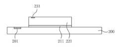
본 발명의 제 4 실시 예에 따른 반도체 패키지의 제조 방법은 9a에 도시된 바와 같이 제 41 접착층(411)을 이용하여 제 4 배선 기판(400) 상에 제 41 반도체 칩(421)을 형성하는 공정을 포함할 수 있다. 상기 제 41 접착층(411)은 제 4 두께(h4)를 가질 수 있다. 상기 41 접착층(411)은 상기 제 4 배선 기판(400) 상에 상기 한 쌍의 제 4 기판 패드(401)와 중첩되지 않도록 형성될 수 있다.A method of manufacturing a semiconductor package according to a fourth embodiment of the present invention includes the steps of forming a forty-
상기 제 41 반도체 칩(421)은 한 쌍의 제 41 칩 패드(431) 및 제 5 두께(h5)를 갖는 제 411 보호막(451)을 포함한다. 상기 제 211 보호막(251)은 연마 공정 및 실장 공정에 의한 상기 제 21 반도체 칩들(221)의 손상을 방지할 수 있다. 상기 제 5 두께(h5)는 10㎛ 내지 20㎛일 수 있다. 상기 제 411 보호막(451)은 상기 한 쌍의 제 41 칩 패드(451)을 노출시키는 한 쌍의 제 41 홀(451a)를 포함할 수 있다.The forty-
이어서, 본 발명의 제 4 실시 예에 따른 반도체 패키지의 제조 방법은 도 9b에 도시된 바와 같이, 상기 제 411 보호막(451)을 제거하고, 제 41 본딩 와이어(441)에 의해 상기 제 41 칩패드(431)와 상기 제 4 기판 패드(401)가 전기적으로 연결되는 공정을 포함할 수 있다.9B, the fourth
다음으로, 본 발명의 제 4 실시 예에 따른 반도체 패키지의 제조 방법은 도 9c에 도시된 바와 같이, 제 42 접착층(412)이 상기 제 41 반도체 칩(421) 상에 형성되는 공정을 포함할 수 있다. 상기 제 42 접착층(412)은 상기 제 4 두께(h4)를 가질 수 있다. 상기 제 4 두께(h4)는 상기 제 41 본딩 와이어(441)의 휨 높이보다 상대적으로 두꺼운 두께일 수 있다. 따라서, 상기 제 4 두께(h4)는 60㎛ 내지 80㎛일 수 있다.Next, a method of manufacturing a semiconductor package according to a fourth embodiment of the present invention may include a process in which a 42th
여기서, 본 발명의 제 4 실시 예에 따른 반도체 패키지의 제조 방법은 상기 제 41 접착측(411)과 상기 제 42 접착층(412)이 동일한 두께를 가지는 것으로 설명된다. 그러나, 상기 제 41 접착층(411)은 하부에 상기 한 쌍의 제 4 본딩 와이어들(441 ~ 444)가 위치하지 않을 수 있다. 따라서, 상기 제 41 접착층(411)은 상기 제 42 접착층(412)보다 상대적으로 얇은 두께를 가질 수 있다. 예를 들어, 상기 제 41 접착층(411)은 상기 제 4 배선 기판(400)과 상기 제 41 반도체 칩(421)을 충분히 접착시킬 수 있는 최소한의 두께일 수 있다. 상기 제 41 접착층(411)은 10㎛ 내지 20㎛의 두께를 가질 수 있다.Here, in the method of manufacturing a semiconductor package according to the fourth embodiment of the present invention, it is described that the 41st
다음으로, 본 발명의 제 4 실시 예에 따른 반도체 패키지의 제조 방법은 도 9d에 도시된 바와 같이, 상기 제 42 접착층(412) 상에 제 42 반도체 칩(422)이 적층되는 공정을 포함할 수 있다. 여기서, 상기 제 42 반도체 칩(422)의 하측 표면은 상기 제 42 접착층(412)의 상기 제 4 두께(h4)에 의해 상기 한 쌍의 제 41 본딩 와이어(441)과 이격될 수 있다.Next, a method of manufacturing a semiconductor package according to a fourth embodiment of the present invention may include a step of stacking a
결과적으로 본 발명의 제 4 실시 예에 따른 반도체 패키지 및 그의 제조 방법은 반도체 칩의 상측 표면을 덮는 연마 공정 및 실장 공정에 의한 손상을 방지하는 보호막을 제거한다. 이어서, 상기 반도체 칩의 상측 표면에 충분한 두께의 접착층을 형성한 후, 다음 반도체 칩을 적층한다. 이에 따라 수직 적층되는 반도체 패키지에 적층되는 다수의 반도체 칩들의 체적이 감소될 수 있다.
As a result, the semiconductor package and the manufacturing method thereof according to the fourth embodiment of the present invention remove the protection film for preventing damage due to the polishing process and the packaging process for covering the upper surface of the semiconductor chip. Subsequently, an adhesive layer having a sufficient thickness is formed on the upper surface of the semiconductor chip, and then the next semiconductor chip is laminated. Whereby the volume of the plurality of semiconductor chips stacked on the vertically stacked semiconductor package can be reduced.
(제 5 실시 예)(Fifth Embodiment)
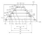
도 10은 본 발명의 제 5 실시 예에 따른 반도체 패키지를 나타낸 단면도이다.10 is a cross-sectional view of a semiconductor package according to a fifth embodiment of the present invention.
도 10을 참조하면, 본 발명의 제 5 실시 예에 따른 반도체 패키지는 제 5 배선 기판(500), 상기 제 5 배선 기판(500)에 적층되며, 서로 상이한 폭을 갖는 다수의 제 5 반도체 칩들(521 ~ 524), 상기 다수의 제 5 반도체 칩들(521 ~ 524) 노출된 상측 표면과 상기 다수의 제 5 반도체 칩들(521 ~ 524) 중 최상측에 위치하는 제 54 반도체 칩(524)의 상측 표면 상에 형성되는 다수의 제 5 보호막들(551p ~ 553p, 554) 및 상기 제 5 반도체 칩들(521 ~ 524)의 측면과 상면을 덮는 제 5 몰딩막(570)을 포함할 수 있다.10, a semiconductor package according to a fifth embodiment of the present invention includes a
여기서, 본 발명의 제 1 실시 예와 유사하게 상기 다수의 제 5 반도체 칩들(521 ~ 524)은 상기 제 5 배선 기판(500)으로부터 멀어지는 순으로 제 51 반도체 칩(521), 제 52 반도체 칩(522), 제 53 반도체 칩(323) 및 제 54 반도체 칩(524)이라 명명한다.Similarly to the first embodiment of the present invention, the
상기 제 5 배선 기판(300) 및 제 5 몰딩막(570)은 본 발명의 제 1 내지 제 4 실시 예에 따른 반도체 패키지의 상기 제 1 배선 기판(100) 및 제 1 몰딩막(170)과 동일한 구성 요소로 이해될 것이다. 따라서, 여기서는 구체적인 설명이 생략된다.The
또한, 본 발명의 제 5 실시 예에 따른 반도체 패키지는 본 발명의 제 1 내지 제 4 실시 예에 따른 반도체 패키지와 유사한 제 5 칩 패드들(531 ~ 534), 제 5 본딩 와이어(541 ~ 544), 제 5 접착층들(511 ~ 514) 및 다수의 제 5 보호막들(551p ~ 553p, 554)이 개시되어 있다. 따라서, 이에 대한 설명은 본 발명의 제 1 내지 제 4 실시 예에서 설명한 내용으로 이해될 수 있을 것이다.In addition, the semiconductor package according to the fifth embodiment of the present invention includes
이하에서는 본 발명의 제 1 내지 제 4 실시 예에 따른 반도체 패키지와 상이한 점만을 간략히 설명하기로 한다.Hereinafter, only the differences from the semiconductor packages according to the first to fourth embodiments of the present invention will be described briefly.
상기 다수의 제 5 반도체 칩들(521 ~ 524)은 서로 상이한 제 1 내지 제 4 폭(w1 ~ w4)을 가질 수 있다. 예를 들면, 상기 제 5 배선 기판(500)에 실장되는 상기 제 51 반도체 칩(521)은 제 1 폭(w1)을 가질 수 있다. 상기 제 51 반도체 칩(521) 상에 적층되는 상기 제 52 반도체 칩(522)은 상기 제 1 폭(w1)보다 상대적으로 작은 제 2 폭(w2)을 가질 수 있다. 상기 제 52 반도체 칩(522) 상에 적층되는 상기 제 53 반도체 칩(523)은 상기 제 2 폭(w2)보다 상대적으로 작은 제 3 폭(w3)을 가질 수 있다. 상기 제 53 반도체 칩(523)의 상에 적층되는 상기 제 54 반도체 칩(524)은 상기 제 3 폭(w3)보다 상대적으로 작은 제 4 폭(w4)을 가질 수 있다. 따라서, 상기 다수의 제 5 반도체 칩들(521 ~ 524)은 상기 제 5 배선 기판(500)으로부터 멀어질수록 작은 폭을 가질 수 있다.The plurality of
본 발명의 제 5 실시 예에 따른 반도체 패키지는 상기 다수의 제 5 반도체 칩들(521 ~ 524)이 피라미드 형태로 적층되는 것으로 도시되어 있다. 그러나, 본 발명의 제 5 실시 예에 따른 반도체 패키지는 상기 다수의 제 5 반도체 칩들(521 ~ 524)이 다양한 형태로 적층될 수 있다.In the semiconductor package according to the fifth embodiment of the present invention, the plurality of
도 11a 내지 11c는 본 발명의 제 5 실시 예에 따른 반도체 패키지의 제조 방법을 순차적으로 나타낸 단면도들이다. 이하에서는 본 발명의 제 1 내지 제 4 실시 예에 따른 반도체 패키지의 제조 방법과 상이한 점만을 간략히 설명한다.11A to 11C are sectional views sequentially illustrating a method of manufacturing a semiconductor package according to a fifth embodiment of the present invention. Hereinafter, only the differences from the manufacturing method of the semiconductor package according to the first to fourth embodiments of the present invention will be described briefly.
본 발명의 제 5 실시 예에 따른 반도체 패키지의 제조 방법은 도 11a에 도시된 바와 같이, 제 5 배선 기판(500)에 제 51 접착층(511)을 이용하여 제 1 폭(w1)을 갖는 제 51 반도체 칩(521)을 실장하는 공정을 포함할 수 있다.11A, a method of manufacturing a semiconductor package according to a fifth embodiment of the present invention is a method of manufacturing a semiconductor package according to a fifth embodiment of the present invention, in which the
이어서, 본 발명의 제 5 실시 예에 따른 반도체 패키지의 제조 방법은 도 11b에 도시된 바와 같이, 상기 제 51 반도체 칩(521) 상에 형성된 제 511 보호막(551)의 일부를 제거하여 제 51 보호막(551p)을 형성하는 공정을 포함할 수 있다. 여기서, 상기 제 511 보호막(251)은 상기 제 1 폭(w1)보다 상대적으로 작은 폭인 제 2 폭(w2)만큼 제거될 수 있다. 상기 제 2 폭(w2)은 후속 공정을 통해 상기 제 51 반도체 칩(521) 상에 적층되는 제 52 반도체 칩(522)의 폭일 수 있다.Next, as shown in FIG. 11B, a method of manufacturing a semiconductor package according to the fifth embodiment of the present invention includes removing a part of the
상기 제 51 보호막(551p)이 형성되는 영역은 상기 제 52 반도체 칩(522)에 의해 노출되는 영역(D4)일 수 있다. 따라서, 상기 제 51 보호막(551p)은 상기 제 51 반도체 칩(521)의 제 51 칩 패드(531)를 노출시키는 제 51 홀(551a)을 포함할 수 있다.The region where the fifty fifth
다음으로, 본 발명의 제 5 실시 예에 따른 반도체 패키지의 제조 방법은 도 11c에 도시된 바와 같이, 상기 제 52 반도체 칩(522)이 상기 제 511 보호막(551)이 제거된 영역에 적층되는 공정을 포함할 수 있다.Next, a method of manufacturing a semiconductor package according to a fifth embodiment of the present invention includes a step of stacking the
결과적으로 본 발명의 제 5 실시 예에 따른 반도체 패키지 및 그의 제조 방법은 연마 공정 및 실장 공정에 의한 손상을 방지하는 보호막을 일부 제거하며, 서로 상이한 폭을 갖는 다수의 반도체 칩들을 적층한다. 이에 따라, 서로 상이한 폭의 다수의 반도체 칩들을 포함하는 반도체 패키지에 적층되는 반도체 칩의 체적을 감소시키는 공정이 최소화될 수 있다.
As a result, the semiconductor package and the manufacturing method thereof according to the fifth embodiment of the present invention partially remove the protective film for preventing damage due to the polishing process and the mounting process, and stack a plurality of semiconductor chips having different widths. Thus, the process of reducing the volume of the semiconductor chip stacked on the semiconductor package including a plurality of semiconductor chips of different widths can be minimized.
(제 6 실시 예)(Sixth Embodiment)
도 12는 본 발명의 제 6 실시 예에 따른 반도체 패키지를 채택하는 전자시스템의 구성도이다.12 is a configuration diagram of an electronic system employing a semiconductor package according to a sixth embodiment of the present invention.
도 12를 참조하면, 본 발명의 제 6 실시 예에 따른 전자시스템(600)은 컨트롤러(610), 입출력장치(620), 기억 장치(630), 인터페이스(640), 및 버스 구조체(650)을 구비할 수 있다. 상기 기억 장치(630)는 도 1 내지 도 11을 참조하여 설명한 것과 유사한 하나 또는 다수의 반도체 패키지를 구비하는 것일 수 있다. 상기 버스 구조체(650)는 상기 컨트롤러(610), 상기 입출력장치(620), 상기 기억 장치(630), 및 상기 인터페이스(640) 상호 간에 데이터들이 이동하는 통로를 제공하는 역할을 할 수 있다.12, an
상기 컨트롤러(610)는 적어도 하나의 마이크로프로세서, 디지털 신호 프로세서, 마이크로 컨트롤러, 그리고 이들과 유사한 기능을 수행할 수 있는 논리 소자들 중에서 적어도 어느 하나를 포함할 수 있다. 상기 입출력장치(620)는 키 패드, 키보드 및 표시 장치(display device) 등에서 선택된 적어도 하나를 포함할 수 있다. 상기 기억 장치(630)는 데이터 및/또는 컨트롤러(610)에 의해 실행되는 명령어 등을 저장하는 역할을 할 수 있다.The
상기 기억 장치(630)는 디램(dynamic random access memory; DRAM) 및 에스램(static random access memory; SRAM)과 같은 휘발성 메모리 칩, 플래시메모리(flash memory), 상변화메모리(phase change memory), 엠램(magnetic random access memory; MRAM), 또는 알램(resistive random access memory; RRAM)과 같은 비휘발성 메모리 칩 및 이들의 조합으로 이루어진 그룹에서 선택된 하나를 구비하는 반도체 패키지를 포함할 수 있다.The
상기 인터페이스(640)는 통신 네트워크로 데이터를 전송하거나 통신 네트워크로부터 데이터를 수신하는 역할을 할 수 있다. 상기 인터페이스(640)는 유무선 형태일 수 있다. 예를 들어, 상기 인터페이스(640)는 안테나 또는 유무선 트랜시버 등을 포함할 수 있다. 상기 전자 시스템(600)에는 응용 칩셋(Application Chipset), 카메라 이미지 프로세서(Camera Image Processor; CIS), 그리고 입출력 장치 등이 더 제공될 수 있다.The
상기 전자 시스템(600)은 모바일 시스템, 개인용 컴퓨터, 산업용 컴퓨터 또는 다양한 기능을 수행하는 로직 시스템(logic system) 등으로 구현될 수 있다. 예컨대, 모바일 시스템은 개인 휴대용 정보 단말기(PDA; Personal Digital Assistant), 휴대용 컴퓨터, 웹 타블렛(web tablet), 모바일폰(mobile phone), 무선폰(wireless phone), 랩톱(laptop) 컴퓨터, 메모리 카드, 디지털 뮤직 시스템(digital music system) 그리고 정보 전송/수신 시스템 중 어느 하나일 수 있다. 상기 전자 시스템(600)이 무선 통신을 수행할 수 있는 장비인 경우에, 상기 전자 시스템(600)은 CDMA(Code Division Multiple Access), GSM(Global System for Mobile communication), NADC(North American Digital Cellular), E-TDMA(Enhanced-Time Division Multiple Access), WCDAM(Wideband Code Division Multiple Access), CDMA2000과 같은 통신 시스템에서 사용될 수 있다.
The
100 : 제 1 배선 기판
101 : 제 1 기판 패드
111 ~ 114 : 제 1 접착층
121 ~ 124 : 제 1 반도체 칩
131 ~ 134 : 제 1 칩 패드
141 ~ 144 : 제 1 본딩 와이어100: first wiring board
101: first substrate pad
111 to 114: first adhesive layer
121 to 124: first semiconductor chip
131 to 134: first chip pad
141 to 144: first bonding wire
Claims (10)
Translated fromKorean상기 다수의 반도체 칩들의 상기 칩 패드들 사이를 전기적으로 연결하는 적어도 하나의 본딩 와이어; 및
상기 다수의 반도체 칩들 각각의 상기 일부 영역 상에 위치하는 다수의 보호막들을 포함하되,
상기 본딩 와이어는 상기 다수의 보호막을 관통하는 반도체 패키지.
A plurality of semiconductor chips on which an upper surface of the chip pad is located and a part of the area where the chip pad is located is exposed;
At least one bonding wire electrically connecting between the chip pads of the plurality of semiconductor chips; And
A plurality of protective films located on the partial areas of each of the plurality of semiconductor chips,
Wherein the bonding wires pass through the plurality of protective films.
상기 다수의 보호막들은 감광성 성분을 구비하는 열경화 폴리머로 형성되는 반도체 패키지.
The method according to claim 1,
Wherein the plurality of protective films are formed of a thermosetting polymer having a photosensitive component.
상기 다수의 반도체 칩들은 계단 형태로 적층되는 반도체 패키지.
The method according to claim 1,
Wherein the plurality of semiconductor chips are stacked in a step-like manner.
상기 다수의 반도체 칩들은 지그재그(zigzag) 형태로 적층되는 반도체 패키지.
The method according to claim 1,
Wherein the plurality of semiconductor chips are stacked in a zigzag form.
상기 다수의 반도체 칩들은 서로 상이한 폭을 갖는 반도체 패키지.
The method according to claim 1,
Wherein the plurality of semiconductor chips have different widths from each other.
상기 다수의 반도체 칩들 중 상대적으로 아래쪽에 위치하는 반도체 칩들은 상대적으로 위쪽에 위치하는 반도체 칩과 비교하여 상대적으로 넓은 폭을 갖는 반도체 패키지.
6. The method of claim 5,
Wherein the semiconductor chips positioned relatively below the plurality of semiconductor chips have a relatively wide width as compared with the semiconductor chips positioned relatively upward.
상기 배선 기판 상에 적층되고, 상측 표면에 위치하는 칩 패드를 포함하는 반도체 칩들;
상기 배선 기판과 상기 반도체 칩들 중 최하측 반도체 칩 사이 및 상기 반도체 칩들 사이에 위치하는 접착층들;
상기 반도체 칩들의 상측 표면 중 상부에 인접한 반도체 칩에 의해 노출되는 영역에 위치하고, 상기 노출되는 영역에 위치하는 칩 패드들을 덮는 제 1 보호막들; 및
상기 반도체 칩들 중 최상측 반도체 칩의 상측 표면에 위치하는 제 2 보호막을 포함하되,
상기 접착층들은 상기 반도체 칩들과 직접 접촉하는 반도체 패키지.
A wiring board;
Semiconductor chips stacked on the wiring board and including chip pads located on the upper surface;
Adhesive layers disposed between the wiring substrate and the lowermost semiconductor chip among the semiconductor chips and between the semiconductor chips;
First protective layers located on a region exposed by the semiconductor chip adjacent to the upper portion of the upper surfaces of the semiconductor chips and covering the chip pads located in the exposed region; And
And a second protective film located on an upper surface of the uppermost semiconductor chip among the semiconductor chips,
Wherein the adhesive layers are in direct contact with the semiconductor chips.
상기 접착층들은 디에이에프(Die Attach Film; DAF)인 반도체 패키지.
8. The method of claim 7,
Wherein the adhesive layers are Die Attach Film (DAF).
상기 배선 기판의 상기 기판 패드가 위치하는 일부 영역이 노출되도록 적층되고, 상측 표면에 위치하는 칩 패드를 포함하는 반도체 칩들;
상기 배선 기판과 상기 반도체 칩들 중 최하측 반도체 칩 사이 및 상기 반도체 칩들 사이에 위치하는 접착층들;
상기 반도체 칩들 각각의 상기 칩 패드가 위치하는 일부 영역을 덮는 보호막들; 및
상기 보호막들을 관통하여, 상기 최하측 반도체 칩의 상기 칩 패드와 상기 기판 패드 사이 및 상기 칩 패드들 사이를 전기적으로 연결하는 본딩 와이어들을 포함하되,
상기 보호막들은 인접하게 적층되는 두 반도체 칩이 중첩되지 않는 영역에만 위치하는 반도체 패키지.
A wiring board including a substrate pad;
Semiconductor chips stacked to expose a portion of the wiring board on which the substrate pads are located and having chip pads located on the upper surface;
Adhesive layers disposed between the wiring substrate and the lowermost semiconductor chip among the semiconductor chips and between the semiconductor chips;
A protective film covering a portion of each of the semiconductor chips where the chip pad is located; And
And bonding wires electrically connecting between the chip pads of the lowermost semiconductor chip and the substrate pads and between the chip pads through the protective films,
Wherein the protective films are located only in regions where two semiconductor chips stacked adjacent to each other do not overlap.
상기 접착층들은 디에이에프(Die Attach Film; DAF)이고, 상기 보호막들은 감광성 폴리이미드(Photo Sensitive Poly Imide; PSPI)인 반도체 패키지.
10. The method of claim 9,
Wherein the adhesive layers are die attach films (DAF), and the protective films are photosensitive polyimide (PSPI).
Priority Applications (2)
| Application Number | Priority Date | Filing Date | Title |
|---|---|---|---|
| KR1020100069117AKR101640832B1 (en) | 2010-07-16 | 2010-07-16 | stacked Semiconductor Package and Method of fabricating the same |
| US13/182,468US8513793B2 (en) | 2010-07-16 | 2011-07-14 | Stacked semiconductor package and method of fabricating the same |
Applications Claiming Priority (1)
| Application Number | Priority Date | Filing Date | Title |
|---|---|---|---|
| KR1020100069117AKR101640832B1 (en) | 2010-07-16 | 2010-07-16 | stacked Semiconductor Package and Method of fabricating the same |
Publications (2)
| Publication Number | Publication Date |
|---|---|
| KR20120008325A KR20120008325A (en) | 2012-01-30 |
| KR101640832B1true KR101640832B1 (en) | 2016-07-19 |
Family
ID=45466329
Family Applications (1)
| Application Number | Title | Priority Date | Filing Date |
|---|---|---|---|
| KR1020100069117AExpired - Fee RelatedKR101640832B1 (en) | 2010-07-16 | 2010-07-16 | stacked Semiconductor Package and Method of fabricating the same |
Country Status (2)
| Country | Link |
|---|---|
| US (1) | US8513793B2 (en) |
| KR (1) | KR101640832B1 (en) |
Families Citing this family (10)
| Publication number | Priority date | Publication date | Assignee | Title |
|---|---|---|---|---|
| US7691668B2 (en)* | 2006-12-19 | 2010-04-06 | Spansion Llc | Method and apparatus for multi-chip packaging |
| KR20150114233A (en) | 2014-04-01 | 2015-10-12 | 삼성전자주식회사 | semiconductor package and method of manufacturing the same |
| KR101471809B1 (en)* | 2014-07-25 | 2014-12-10 | 조광섭 | Bag filter cleaning system for dust collector having two control valves and compressed air pipes separated from one another |
| US11171114B2 (en)* | 2015-12-02 | 2021-11-09 | Intel Corporation | Die stack with cascade and vertical connections |
| KR102499954B1 (en) | 2016-10-24 | 2023-02-15 | 삼성전자주식회사 | Multi-chip package and method of manufacturing the same |
| KR102578797B1 (en) | 2018-02-01 | 2023-09-18 | 삼성전자주식회사 | Semiconductor package |
| KR20200022214A (en)* | 2018-08-22 | 2020-03-03 | 삼성전자주식회사 | Semiconductor package and a method for manufacturing the same |
| CN111180424A (en)* | 2018-11-13 | 2020-05-19 | 长鑫存储技术有限公司 | Stacked structure, semiconductor package structure and fabrication process of the stacked structure |
| KR102742639B1 (en) | 2020-07-17 | 2024-12-16 | 삼성전자주식회사 | Semiconductor package |
| US20230260949A1 (en)* | 2022-02-16 | 2023-08-17 | Western Digital Technologies, Inc. | Semiconductor Device with Protective Layer |
Family Cites Families (16)
| Publication number | Priority date | Publication date | Assignee | Title |
|---|---|---|---|---|
| KR100451950B1 (en) | 2002-02-25 | 2004-10-08 | 삼성전자주식회사 | Sawing method for image sensor device wafer |
| JP3831287B2 (en) | 2002-04-08 | 2006-10-11 | 株式会社日立製作所 | Manufacturing method of semiconductor device |
| KR100486290B1 (en) | 2002-12-23 | 2005-04-29 | 삼성전자주식회사 | Assembling method of semiconductor package and removal apparatus of protection tape in semiconductor process |
| DE102004049356B4 (en)* | 2004-10-08 | 2006-06-29 | Infineon Technologies Ag | Semiconductor module with an internal semiconductor chip stack and method for producing the same |
| KR20080014302A (en)* | 2006-08-10 | 2008-02-14 | 삼성전자주식회사 | Die attach method using fiber reinforced polymer |
| TWI327365B (en)* | 2007-01-19 | 2010-07-11 | Chipmos Technologies Inc | Zigzag-stacked chip package structure |
| US8723332B2 (en)* | 2007-06-11 | 2014-05-13 | Invensas Corporation | Electrically interconnected stacked die assemblies |
| KR100886717B1 (en)* | 2007-10-16 | 2009-03-04 | 주식회사 하이닉스반도체 | Laminated semiconductor package and method for manufacturing same |
| JP5529371B2 (en)* | 2007-10-16 | 2014-06-25 | ピーエスフォー ルクスコ エスエイアールエル | Semiconductor device and manufacturing method thereof |
| US7952183B2 (en)* | 2007-10-29 | 2011-05-31 | Kabushiki Kaisha Toshiba | High capacity memory with stacked layers |
| JP2009246218A (en)* | 2008-03-31 | 2009-10-22 | Renesas Technology Corp | Semiconductor device and method for manufacturing the same |
| US7687921B2 (en)* | 2008-05-05 | 2010-03-30 | Super Talent Electronics, Inc. | High density memory device manufacturing using isolated step pads |
| KR100997787B1 (en)* | 2008-06-30 | 2010-12-02 | 주식회사 하이닉스반도체 | Laminated Semiconductor Package and Method of Manufacturing the Same |
| KR20100049283A (en)* | 2008-11-03 | 2010-05-12 | 삼성전자주식회사 | Semiconductor package and method for manufacturing of the same |
| KR20100134354A (en)* | 2009-06-15 | 2010-12-23 | 삼성전자주식회사 | Semiconductor Packages, Stack Modules, Cards & Electronic Systems |
| KR101686553B1 (en)* | 2010-07-12 | 2016-12-14 | 삼성전자 주식회사 | Chip Stacked Package and Package on Package |
- 2010
- 2010-07-16KRKR1020100069117Apatent/KR101640832B1/ennot_activeExpired - Fee Related
- 2011
- 2011-07-14USUS13/182,468patent/US8513793B2/ennot_activeExpired - Fee Related
Also Published As
| Publication number | Publication date |
|---|---|
| US20120013026A1 (en) | 2012-01-19 |
| KR20120008325A (en) | 2012-01-30 |
| US8513793B2 (en) | 2013-08-20 |
Similar Documents
| Publication | Publication Date | Title |
|---|---|---|
| KR101640832B1 (en) | stacked Semiconductor Package and Method of fabricating the same | |
| KR101805114B1 (en) | Integrated circuit packaging system with dual side connection and method of manufacture thereof | |
| KR101686553B1 (en) | Chip Stacked Package and Package on Package | |
| US9397070B2 (en) | Method for forming package structure | |
| US7560857B2 (en) | Package structure of MEMS microphone | |
| US20080042253A1 (en) | Stack type ball grid array package and method for manufacturing the same | |
| KR20100049283A (en) | Semiconductor package and method for manufacturing of the same | |
| US8043894B2 (en) | Integrated circuit package system with redistribution layer | |
| US9485868B2 (en) | Package structure | |
| US20080179730A1 (en) | Wafer Level CSP Packaging Concept | |
| KR20100109241A (en) | Chip stack package and fabrication method thereof | |
| JP2002057241A (en) | Semiconductor package including transplantable conductive pattern, and manufacturing method thereof | |
| US20080217759A1 (en) | Chip package substrate and structure thereof | |
| US20090283890A1 (en) | Semiconductor multi-package module including tape substrate land grid array package stacked over ball grid array package | |
| KR101473905B1 (en) | Integrated circuit package system with offset stacked die | |
| US20080315406A1 (en) | Integrated circuit package system with cavity substrate | |
| US6784534B1 (en) | Thin integrated circuit package having an optically transparent window | |
| US20100029046A1 (en) | Integrated circuit package system with concave terminal | |
| KR100924554B1 (en) | Flip chip package and manufacturing method thereof | |
| US20120286410A1 (en) | Semiconductor device packaging method and semiconductor device package | |
| US9177898B2 (en) | Integrated circuit package system with locking terminal | |
| KR20150043931A (en) | Semiconductor package | |
| US8937393B2 (en) | Integrated circuit package system with device cavity | |
| US6689637B2 (en) | Method of manufacturing a multi-chip semiconductor package | |
| KR100456815B1 (en) | Semiconductor package and method for attaching chip |
Legal Events
| Date | Code | Title | Description |
|---|---|---|---|
| PA0109 | Patent application | St.27 status event code:A-0-1-A10-A12-nap-PA0109 | |
| PG1501 | Laying open of application | St.27 status event code:A-1-1-Q10-Q12-nap-PG1501 | |
| R18-X000 | Changes to party contact information recorded | St.27 status event code:A-3-3-R10-R18-oth-X000 | |
| A201 | Request for examination | ||
| PA0201 | Request for examination | St.27 status event code:A-1-2-D10-D11-exm-PA0201 | |
| E902 | Notification of reason for refusal | ||
| PE0902 | Notice of grounds for rejection | St.27 status event code:A-1-2-D10-D21-exm-PE0902 | |
| P11-X000 | Amendment of application requested | St.27 status event code:A-2-2-P10-P11-nap-X000 | |
| P13-X000 | Application amended | St.27 status event code:A-2-2-P10-P13-nap-X000 | |
| R17-X000 | Change to representative recorded | St.27 status event code:A-3-3-R10-R17-oth-X000 | |
| R17-X000 | Change to representative recorded | St.27 status event code:A-3-3-R10-R17-oth-X000 | |
| PE0701 | Decision of registration | St.27 status event code:A-1-2-D10-D22-exm-PE0701 | |
| GRNT | Written decision to grant | ||
| PR0701 | Registration of establishment | St.27 status event code:A-2-4-F10-F11-exm-PR0701 | |
| PR1002 | Payment of registration fee | St.27 status event code:A-2-2-U10-U11-oth-PR1002 Fee payment year number:1 | |
| PG1601 | Publication of registration | St.27 status event code:A-4-4-Q10-Q13-nap-PG1601 | |
| PC1903 | Unpaid annual fee | St.27 status event code:A-4-4-U10-U13-oth-PC1903 Not in force date:20190714 Payment event data comment text:Termination Category : DEFAULT_OF_REGISTRATION_FEE | |
| PC1903 | Unpaid annual fee | St.27 status event code:N-4-6-H10-H13-oth-PC1903 Ip right cessation event data comment text:Termination Category : DEFAULT_OF_REGISTRATION_FEE Not in force date:20190714 |